US4188438A - Antioxidant coating of copper parts for thermal compression gang bonding of semiconductive devices - Google Patents
Antioxidant coating of copper parts for thermal compression gang bonding of semiconductive devicesDownload PDFInfo
- Publication number
- US4188438A US4188438AUS05/582,634US58263475AUS4188438AUS 4188438 AUS4188438 AUS 4188438AUS 58263475 AUS58263475 AUS 58263475AUS 4188438 AUS4188438 AUS 4188438A
- Authority
- US
- United States
- Prior art keywords
- thermal compression
- copper
- bonding
- antioxidant coating
- gang
- Prior art date
- Legal status (The legal status is an assumption and is not a legal conclusion. Google has not performed a legal analysis and makes no representation as to the accuracy of the status listed.)
- Expired - Lifetime
Links
- RYGMFSIKBFXOCR-UHFFFAOYSA-NCopperChemical group[Cu]RYGMFSIKBFXOCR-UHFFFAOYSA-N0.000titleclaimsabstractdescription70
- 230000006835compressionEffects0.000titleclaimsabstractdescription52
- 238000007906compressionMethods0.000titleclaimsabstractdescription52
- 239000003963antioxidant agentSubstances0.000titleclaimsabstractdescription42
- 230000003078antioxidant effectEffects0.000titleclaimsabstractdescription42
- 238000000576coating methodMethods0.000titleclaimsabstractdescription42
- 239000011248coating agentSubstances0.000titleclaimsabstractdescription36
- 229910052802copperInorganic materials0.000claimsabstractdescription63
- 239000010949copperSubstances0.000claimsabstractdescription63
- 229910052737goldInorganic materials0.000claimsabstractdescription23
- 239000010931goldSubstances0.000claimsabstractdescription23
- PCHJSUWPFVWCPO-UHFFFAOYSA-NgoldChemical compound[Au]PCHJSUWPFVWCPO-UHFFFAOYSA-N0.000claimsabstractdescription21
- 239000000463materialSubstances0.000claimsabstractdescription12
- RAOSIAYCXKBGFE-UHFFFAOYSA-K[Cu+3].[O-]P([O-])([O-])=OChemical compound[Cu+3].[O-]P([O-])([O-])=ORAOSIAYCXKBGFE-UHFFFAOYSA-K0.000claimsabstractdescription9
- ZCDOYSPFYFSLEW-UHFFFAOYSA-Nchromate(2-)Chemical compound[O-][Cr]([O-])(=O)=OZCDOYSPFYFSLEW-UHFFFAOYSA-N0.000claimsabstractdescription7
- 238000000034methodMethods0.000claimsdescription17
- 238000001465metallisationMethods0.000claimsdescription5
- 230000003647oxidationEffects0.000claimsdescription3
- 238000007254oxidation reactionMethods0.000claimsdescription3
- 230000000630rising effectEffects0.000claimsdescription3
- 229910052751metalInorganic materials0.000claims8
- 239000002184metalSubstances0.000claims8
- VYZAMTAEIAYCRO-UHFFFAOYSA-NChromiumChemical compound[Cr]VYZAMTAEIAYCRO-UHFFFAOYSA-N0.000claims1
- 229910052804chromiumInorganic materials0.000claims1
- 239000011651chromiumSubstances0.000claims1
- PXHVJJICTQNCMI-UHFFFAOYSA-NNickelChemical compound[Ni]PXHVJJICTQNCMI-UHFFFAOYSA-N0.000description6
- VYPSYNLAJGMNEJ-UHFFFAOYSA-NSilicium dioxideChemical compoundO=[Si]=OVYPSYNLAJGMNEJ-UHFFFAOYSA-N0.000description6
- 239000008367deionised waterSubstances0.000description4
- 229910021641deionized waterInorganic materials0.000description4
- XLYOFNOQVPJJNP-UHFFFAOYSA-NwaterChemical compoundOXLYOFNOQVPJJNP-UHFFFAOYSA-N0.000description4
- VEXZGXHMUGYJMC-UHFFFAOYSA-NHydrochloric acidChemical compoundClVEXZGXHMUGYJMC-UHFFFAOYSA-N0.000description3
- 229910052759nickelInorganic materials0.000description3
- 239000000377silicon dioxideSubstances0.000description3
- 235000012239silicon dioxideNutrition0.000description3
- LTPBRCUWZOMYOC-UHFFFAOYSA-NBeryllium oxideChemical compoundO=[Be]LTPBRCUWZOMYOC-UHFFFAOYSA-N0.000description2
- QPLDLSVMHZLSFG-UHFFFAOYSA-NCopper oxideChemical compound[Cu]=OQPLDLSVMHZLSFG-UHFFFAOYSA-N0.000description2
- 239000005751Copper oxideSubstances0.000description2
- 229910003556H2 SO4Inorganic materials0.000description2
- NBIIXXVUZAFLBC-UHFFFAOYSA-NPhosphoric acidChemical compoundOP(O)(O)=ONBIIXXVUZAFLBC-UHFFFAOYSA-N0.000description2
- 239000002253acidSubstances0.000description2
- 239000000956alloySubstances0.000description2
- 229910045601alloyInorganic materials0.000description2
- KRVSOGSZCMJSLX-UHFFFAOYSA-Lchromic acidSubstancesO[Cr](O)(=O)=OKRVSOGSZCMJSLX-UHFFFAOYSA-L0.000description2
- 238000004140cleaningMethods0.000description2
- 229910000431copper oxideInorganic materials0.000description2
- 238000009713electroplatingMethods0.000description2
- 239000011888foilSubstances0.000description2
- AWJWCTOOIBYHON-UHFFFAOYSA-Nfuro[3,4-b]pyrazine-5,7-dioneChemical compoundC1=CN=C2C(=O)OC(=O)C2=N1AWJWCTOOIBYHON-UHFFFAOYSA-N0.000description2
- 239000011521glassSubstances0.000description2
- 238000010438heat treatmentMethods0.000description2
- 238000007654immersionMethods0.000description2
- 229910000833kovarInorganic materials0.000description2
- 238000002161passivationMethods0.000description2
- 239000004593EpoxySubstances0.000description1
- 239000004642PolyimideSubstances0.000description1
- 230000002411adverseEffects0.000description1
- XAGFODPZIPBFFR-UHFFFAOYSA-NaluminiumChemical compound[Al]XAGFODPZIPBFFR-UHFFFAOYSA-N0.000description1
- 229910052782aluminiumInorganic materials0.000description1
- 229910000147aluminium phosphateInorganic materials0.000description1
- 230000004888barrier functionEffects0.000description1
- 239000000919ceramicSubstances0.000description1
- 239000011889copper foilSubstances0.000description1
- 239000000203mixtureSubstances0.000description1
- 239000002985plastic filmSubstances0.000description1
- 229920006255plastic filmPolymers0.000description1
- 238000007747platingMethods0.000description1
- 229920001721polyimidePolymers0.000description1
- 239000004065semiconductorSubstances0.000description1
- 238000010008shearingMethods0.000description1
- 239000000758substrateSubstances0.000description1
- 230000003746surface roughnessEffects0.000description1
Images

Classifications
- H—ELECTRICITY
- H01—ELECTRIC ELEMENTS
- H01L—SEMICONDUCTOR DEVICES NOT COVERED BY CLASS H10
- H01L24/00—Arrangements for connecting or disconnecting semiconductor or solid-state bodies; Methods or apparatus related thereto
- H01L24/01—Means for bonding being attached to, or being formed on, the surface to be connected, e.g. chip-to-package, die-attach, "first-level" interconnects; Manufacturing methods related thereto
- H01L24/10—Bump connectors ; Manufacturing methods related thereto
- H01L24/12—Structure, shape, material or disposition of the bump connectors prior to the connecting process
- H01L24/13—Structure, shape, material or disposition of the bump connectors prior to the connecting process of an individual bump connector
- H—ELECTRICITY
- H01—ELECTRIC ELEMENTS
- H01L—SEMICONDUCTOR DEVICES NOT COVERED BY CLASS H10
- H01L24/00—Arrangements for connecting or disconnecting semiconductor or solid-state bodies; Methods or apparatus related thereto
- H01L24/80—Methods for connecting semiconductor or other solid state bodies using means for bonding being attached to, or being formed on, the surface to be connected
- H01L24/86—Methods for connecting semiconductor or other solid state bodies using means for bonding being attached to, or being formed on, the surface to be connected using tape automated bonding [TAB]
- H—ELECTRICITY
- H01—ELECTRIC ELEMENTS
- H01L—SEMICONDUCTOR DEVICES NOT COVERED BY CLASS H10
- H01L2224/00—Indexing scheme for arrangements for connecting or disconnecting semiconductor or solid-state bodies and methods related thereto as covered by H01L24/00
- H01L2224/01—Means for bonding being attached to, or being formed on, the surface to be connected, e.g. chip-to-package, die-attach, "first-level" interconnects; Manufacturing methods related thereto
- H01L2224/02—Bonding areas; Manufacturing methods related thereto
- H01L2224/04—Structure, shape, material or disposition of the bonding areas prior to the connecting process
- H01L2224/05—Structure, shape, material or disposition of the bonding areas prior to the connecting process of an individual bonding area
- H01L2224/0554—External layer
- H01L2224/05599—Material
- H01L2224/056—Material with a principal constituent of the material being a metal or a metalloid, e.g. boron [B], silicon [Si], germanium [Ge], arsenic [As], antimony [Sb], tellurium [Te] and polonium [Po], and alloys thereof
- H01L2224/05617—Material with a principal constituent of the material being a metal or a metalloid, e.g. boron [B], silicon [Si], germanium [Ge], arsenic [As], antimony [Sb], tellurium [Te] and polonium [Po], and alloys thereof the principal constituent melting at a temperature of greater than or equal to 400°C and less than 950°C
- H01L2224/05624—Aluminium [Al] as principal constituent
- H—ELECTRICITY
- H01—ELECTRIC ELEMENTS
- H01L—SEMICONDUCTOR DEVICES NOT COVERED BY CLASS H10
- H01L2224/00—Indexing scheme for arrangements for connecting or disconnecting semiconductor or solid-state bodies and methods related thereto as covered by H01L24/00
- H01L2224/01—Means for bonding being attached to, or being formed on, the surface to be connected, e.g. chip-to-package, die-attach, "first-level" interconnects; Manufacturing methods related thereto
- H01L2224/10—Bump connectors; Manufacturing methods related thereto
- H01L2224/12—Structure, shape, material or disposition of the bump connectors prior to the connecting process
- H01L2224/13—Structure, shape, material or disposition of the bump connectors prior to the connecting process of an individual bump connector
- H01L2224/13001—Core members of the bump connector
- H01L2224/13099—Material
- H01L2224/131—Material with a principal constituent of the material being a metal or a metalloid, e.g. boron [B], silicon [Si], germanium [Ge], arsenic [As], antimony [Sb], tellurium [Te] and polonium [Po], and alloys thereof
- H01L2224/13138—Material with a principal constituent of the material being a metal or a metalloid, e.g. boron [B], silicon [Si], germanium [Ge], arsenic [As], antimony [Sb], tellurium [Te] and polonium [Po], and alloys thereof the principal constituent melting at a temperature of greater than or equal to 950°C and less than 1550°C
- H01L2224/13147—Copper [Cu] as principal constituent
- H—ELECTRICITY
- H01—ELECTRIC ELEMENTS
- H01L—SEMICONDUCTOR DEVICES NOT COVERED BY CLASS H10
- H01L24/00—Arrangements for connecting or disconnecting semiconductor or solid-state bodies; Methods or apparatus related thereto
- H01L24/01—Means for bonding being attached to, or being formed on, the surface to be connected, e.g. chip-to-package, die-attach, "first-level" interconnects; Manufacturing methods related thereto
- H01L24/50—Tape automated bonding [TAB] connectors, i.e. film carriers; Manufacturing methods related thereto
- H—ELECTRICITY
- H01—ELECTRIC ELEMENTS
- H01L—SEMICONDUCTOR DEVICES NOT COVERED BY CLASS H10
- H01L24/00—Arrangements for connecting or disconnecting semiconductor or solid-state bodies; Methods or apparatus related thereto
- H01L24/74—Apparatus for manufacturing arrangements for connecting or disconnecting semiconductor or solid-state bodies
- H01L24/79—Apparatus for Tape Automated Bonding [TAB]
- H—ELECTRICITY
- H01—ELECTRIC ELEMENTS
- H01L—SEMICONDUCTOR DEVICES NOT COVERED BY CLASS H10
- H01L2924/00—Indexing scheme for arrangements or methods for connecting or disconnecting semiconductor or solid-state bodies as covered by H01L24/00
- H01L2924/01—Chemical elements
- H01L2924/01005—Boron [B]
- H—ELECTRICITY
- H01—ELECTRIC ELEMENTS
- H01L—SEMICONDUCTOR DEVICES NOT COVERED BY CLASS H10
- H01L2924/00—Indexing scheme for arrangements or methods for connecting or disconnecting semiconductor or solid-state bodies as covered by H01L24/00
- H01L2924/01—Chemical elements
- H01L2924/01006—Carbon [C]
- H—ELECTRICITY
- H01—ELECTRIC ELEMENTS
- H01L—SEMICONDUCTOR DEVICES NOT COVERED BY CLASS H10
- H01L2924/00—Indexing scheme for arrangements or methods for connecting or disconnecting semiconductor or solid-state bodies as covered by H01L24/00
- H01L2924/01—Chemical elements
- H01L2924/01013—Aluminum [Al]
- H—ELECTRICITY
- H01—ELECTRIC ELEMENTS
- H01L—SEMICONDUCTOR DEVICES NOT COVERED BY CLASS H10
- H01L2924/00—Indexing scheme for arrangements or methods for connecting or disconnecting semiconductor or solid-state bodies as covered by H01L24/00
- H01L2924/01—Chemical elements
- H01L2924/01015—Phosphorus [P]
- H—ELECTRICITY
- H01—ELECTRIC ELEMENTS
- H01L—SEMICONDUCTOR DEVICES NOT COVERED BY CLASS H10
- H01L2924/00—Indexing scheme for arrangements or methods for connecting or disconnecting semiconductor or solid-state bodies as covered by H01L24/00
- H01L2924/01—Chemical elements
- H01L2924/01019—Potassium [K]
- H—ELECTRICITY
- H01—ELECTRIC ELEMENTS
- H01L—SEMICONDUCTOR DEVICES NOT COVERED BY CLASS H10
- H01L2924/00—Indexing scheme for arrangements or methods for connecting or disconnecting semiconductor or solid-state bodies as covered by H01L24/00
- H01L2924/01—Chemical elements
- H01L2924/01023—Vanadium [V]
- H—ELECTRICITY
- H01—ELECTRIC ELEMENTS
- H01L—SEMICONDUCTOR DEVICES NOT COVERED BY CLASS H10
- H01L2924/00—Indexing scheme for arrangements or methods for connecting or disconnecting semiconductor or solid-state bodies as covered by H01L24/00
- H01L2924/01—Chemical elements
- H01L2924/01024—Chromium [Cr]
- H—ELECTRICITY
- H01—ELECTRIC ELEMENTS
- H01L—SEMICONDUCTOR DEVICES NOT COVERED BY CLASS H10
- H01L2924/00—Indexing scheme for arrangements or methods for connecting or disconnecting semiconductor or solid-state bodies as covered by H01L24/00
- H01L2924/01—Chemical elements
- H01L2924/01029—Copper [Cu]
- H—ELECTRICITY
- H01—ELECTRIC ELEMENTS
- H01L—SEMICONDUCTOR DEVICES NOT COVERED BY CLASS H10
- H01L2924/00—Indexing scheme for arrangements or methods for connecting or disconnecting semiconductor or solid-state bodies as covered by H01L24/00
- H01L2924/01—Chemical elements
- H01L2924/01033—Arsenic [As]
- H—ELECTRICITY
- H01—ELECTRIC ELEMENTS
- H01L—SEMICONDUCTOR DEVICES NOT COVERED BY CLASS H10
- H01L2924/00—Indexing scheme for arrangements or methods for connecting or disconnecting semiconductor or solid-state bodies as covered by H01L24/00
- H01L2924/01—Chemical elements
- H01L2924/01039—Yttrium [Y]
- H—ELECTRICITY
- H01—ELECTRIC ELEMENTS
- H01L—SEMICONDUCTOR DEVICES NOT COVERED BY CLASS H10
- H01L2924/00—Indexing scheme for arrangements or methods for connecting or disconnecting semiconductor or solid-state bodies as covered by H01L24/00
- H01L2924/01—Chemical elements
- H01L2924/01078—Platinum [Pt]
- H—ELECTRICITY
- H01—ELECTRIC ELEMENTS
- H01L—SEMICONDUCTOR DEVICES NOT COVERED BY CLASS H10
- H01L2924/00—Indexing scheme for arrangements or methods for connecting or disconnecting semiconductor or solid-state bodies as covered by H01L24/00
- H01L2924/01—Chemical elements
- H01L2924/01079—Gold [Au]
- H—ELECTRICITY
- H01—ELECTRIC ELEMENTS
- H01L—SEMICONDUCTOR DEVICES NOT COVERED BY CLASS H10
- H01L2924/00—Indexing scheme for arrangements or methods for connecting or disconnecting semiconductor or solid-state bodies as covered by H01L24/00
- H01L2924/01—Chemical elements
- H01L2924/01082—Lead [Pb]
- H—ELECTRICITY
- H01—ELECTRIC ELEMENTS
- H01L—SEMICONDUCTOR DEVICES NOT COVERED BY CLASS H10
- H01L2924/00—Indexing scheme for arrangements or methods for connecting or disconnecting semiconductor or solid-state bodies as covered by H01L24/00
- H01L2924/10—Details of semiconductor or other solid state devices to be connected
- H01L2924/11—Device type
- H01L2924/14—Integrated circuits
- Y—GENERAL TAGGING OF NEW TECHNOLOGICAL DEVELOPMENTS; GENERAL TAGGING OF CROSS-SECTIONAL TECHNOLOGIES SPANNING OVER SEVERAL SECTIONS OF THE IPC; TECHNICAL SUBJECTS COVERED BY FORMER USPC CROSS-REFERENCE ART COLLECTIONS [XRACs] AND DIGESTS
- Y10—TECHNICAL SUBJECTS COVERED BY FORMER USPC
- Y10S—TECHNICAL SUBJECTS COVERED BY FORMER USPC CROSS-REFERENCE ART COLLECTIONS [XRACs] AND DIGESTS
- Y10S428/00—Stock material or miscellaneous articles
- Y10S428/901—Printed circuit
- Y—GENERAL TAGGING OF NEW TECHNOLOGICAL DEVELOPMENTS; GENERAL TAGGING OF CROSS-SECTIONAL TECHNOLOGIES SPANNING OVER SEVERAL SECTIONS OF THE IPC; TECHNICAL SUBJECTS COVERED BY FORMER USPC CROSS-REFERENCE ART COLLECTIONS [XRACs] AND DIGESTS
- Y10—TECHNICAL SUBJECTS COVERED BY FORMER USPC
- Y10T—TECHNICAL SUBJECTS COVERED BY FORMER US CLASSIFICATION
- Y10T29/00—Metal working
- Y10T29/49—Method of mechanical manufacture
- Y10T29/49002—Electrical device making
- Y10T29/49117—Conductor or circuit manufacturing
- Y10T29/49121—Beam lead frame or beam lead device
- Y—GENERAL TAGGING OF NEW TECHNOLOGICAL DEVELOPMENTS; GENERAL TAGGING OF CROSS-SECTIONAL TECHNOLOGIES SPANNING OVER SEVERAL SECTIONS OF THE IPC; TECHNICAL SUBJECTS COVERED BY FORMER USPC CROSS-REFERENCE ART COLLECTIONS [XRACs] AND DIGESTS
- Y10—TECHNICAL SUBJECTS COVERED BY FORMER USPC
- Y10T—TECHNICAL SUBJECTS COVERED BY FORMER US CLASSIFICATION
- Y10T29/00—Metal working
- Y10T29/49—Method of mechanical manufacture
- Y10T29/49002—Electrical device making
- Y10T29/49117—Conductor or circuit manufacturing
- Y10T29/49169—Assembling electrical component directly to terminal or elongated conductor
- Y—GENERAL TAGGING OF NEW TECHNOLOGICAL DEVELOPMENTS; GENERAL TAGGING OF CROSS-SECTIONAL TECHNOLOGIES SPANNING OVER SEVERAL SECTIONS OF THE IPC; TECHNICAL SUBJECTS COVERED BY FORMER USPC CROSS-REFERENCE ART COLLECTIONS [XRACs] AND DIGESTS
- Y10—TECHNICAL SUBJECTS COVERED BY FORMER USPC
- Y10T—TECHNICAL SUBJECTS COVERED BY FORMER US CLASSIFICATION
- Y10T428/00—Stock material or miscellaneous articles
- Y10T428/24—Structurally defined web or sheet [e.g., overall dimension, etc.]
- Y10T428/24802—Discontinuous or differential coating, impregnation or bond [e.g., artwork, printing, retouched photograph, etc.]
- Y10T428/24917—Discontinuous or differential coating, impregnation or bond [e.g., artwork, printing, retouched photograph, etc.] including metal layer
Definitions
- the present inventionrelates in general to thermal compression gang bonding of semiconductive devices and, more particularly, to gang bonding of copper members associated with the semiconductive device, such copper members including, for example, the lead frame, interconnect leads and the gang bonding bumps on the semiconductive device.
- thermal compression gang bonding of semiconductive deviceshas been accomplished.
- a copper pattern of ribbon-shaped interconnect leadswas coated with a nickel layer and the nickel layer was plated with gold to a thickness within the range of 30-60 microinches.
- the interconnect ribbon leadswere then gang bonded to gold gang bonding bumps carried from and rising above the surface of the semiconductive device to be gang bonded.
- the nickel layerserved as a barrier under the gold layer so that a gold-to-gold bond was obtained between the gold plated copper interconnect lead and the gold gang bonding bump.
- a similar gold-to-gold thermal compression bondwas obtained at the outer end of the interconnect lead between the interconnect lead and the lead frame.
- the principal object of the present inventionis the provision of an improved method for thermal compression gang bonding of copper portions of structures to be connected to a semiconductor device.
- copper portions of structures for interconnecting a semiconductive device to a circuitare thermal compression gang bonded through a very thin antioxidant coating over the copper, such coating being of a material and thickness compatible with thermal compression bonding therethrough to the underlying copper.
- copper gang bonding bumpsprovided on a semiconductive device for thermal compression bonding to lead structures, are coated with an antioxidant coating of a material and thickness which is compatible with thermal compression bonding through the antioxidant coating to the underlying copper so that the copper forms a bonding interface with the bonded lead structure.
- the antioxidant coating for the copper portion of the thermal compression bondis selected from the group consisting of gold, chromate, and copper phosphate.
- the interconnect lead structure which is to be bonded at its inner end to gang bonding bumps on the semicondutive deviceis made of copper and has a thin antioxidant coating thereon, the material and the thickness of the antioxidant coating being compatible with a thermal compression bonding therethrough to the copper interconnect lead structure.
- a lead frame structurefor thermal compression gang bonding to the outer regions of a metallic interconnect lead structure, is made of copper or includes a copper layer to which a bond is to be made, such copper portion of the lead frame structure being coated with an antioxidant coating of a material and of a thickness compatible with thermal compression gang bonding therethrough so that the bonding interface is made to the copper portion of the lead frame structure.
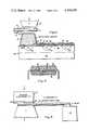
- FIG. 1is a plan view of a film type gang bonding tape having the metallic interconnect lead patterns thereon for thermal compression bonding to semiconductive chips or dies by an automatic gang bonding machine,
- FIG. 2is an enlarged plan view of a portion of the structure of FIG. 1 delineated by line 2--2,
- FIG. 3is an enlarged sectional view of a thermal compression die bonding head for gang bonding the interconnect lead structures to gang bonding bumps on the semiconductive chip or die,
- FIG. 4is an enlarged detail view of a portion of the structure of FIG. 3 delineated by line 4--4,
- FIG. 5is a sectional view of an integrated circuit package having an integrated circuit die or chip mounted to a lead frame structure therein, and
- FIG. 6is an enlarged detail view of a portion of the structure of FIG. 5 delineated by line 6--6.
- the bonding tape 11for use in an automatic thermal compression gang bonding machine for attaching the interconnect leads to the die.
- the tape 11includes a wrought copper sheet 12 perforated at 13 along its opposite marginal edges to receive a sprocket drive wheel therein for advancing the tape from a supply reel through the automatic gang bonding machine.
- a plurality of interconnect lead patterns of metallic foil 14are formed in the wrought copper foil 12, the typical pattern being shown in FIG. 2.
- a polyimide plastic film 15is adhered to the underside of the copper sheet 12 for holding the interconnect lead portions 16 of the pattern 14 in the desired positions.
- a rectangular central aperture 18is provided in the film 15 with the inner ends of the interconnect lead ribbons 16 extending over the lip of the rectangular aperture 18.
- a plurality of perforations 19are disposed about the periphery of the interconnect lead patterns 14 to facilitate shearing of the foil 12 and film 15 in a subsequent step of the bonding process.
- FIGS. 3 and 4there is shown the die bonding machine for thermal compression gang bonding of the inner ends of the interconnect leads 16 to a plurality of gang bonding bumps 21 disposed about the periphery of a die or semiconductive chip 22.
- the individual chips 22include a semiconductive substrate portion 23 having an epitaxial n type conductivity region 24 grown thereon. A plurality of p+ conductivity regions 25 are diffused into the n region 24. An n+ conductivity region 26 is diffused into the n epitaxial layer 24 for making electrical contact thereto. The upper surface of the n layer 24 is coated with a passivation layer 27 of silicon dioxide.
- a plurality of apertures 29are provided in the silicon dioxide layer 27 in registration with certain of the regions 25 and 26 and an interconnect pattern of metallization 28, as of aluminum, is deposited through the apertures 29 for making electrical contact to the n+ and p+ type regions.
- the gang bonding bumps 21are deposited, as by electroplating, over the intraconnect pattern of metallization 28 for making electrical contact thereto.
- the gang bonding bumps 21are one to two mils high and have a cross-section at their base of approximately 12 square mils.
- the intraconnect pattern of metallization 28is covered over with a second passivation layer 31, as of silicon dioxide.
- the semiconductive die or chip 22is carried from a glass plate 33 via a high temperature film 34 joined to the glass plate 33 via wax 35.
- the dieis carried from the film 34 via the intermediary of a layer of release wax 36.
- the assemblyis scored by saw kerfs passing through the release wax and partially into the high temperature film 34.
- the die bonding machinebrings the individual chips, to be bonded, into registration with a die bonding tool 38, as of beryllia ceramic, heated to a temperature of, for example, 550° C. for gang bonding.
- the tool 38is caused to press the inner ends of the interconnect leads 16 down onto the upper ends of the gang bonding bumps 21 with a pressure of approximately 100 grams per bump or 8 grams per square mil for a time of approximately 0.2 seconds.
- the bonding tool 38gang bonds 14 gang bonding bumps 21 simultaneously.
- Chromatic antioxidant coatingsare applied to the copper portions by cleaning the copper portions with hydrochloric acid and then immersing the copper parts or devices having exposed copper parts in a plating solution of chromic acid mixed with H 2 SO 4 acid such mixture being 2.0% chromic acid to 8.0% full strength H 2 SO 4 acid to 90% deionized water by volume. The parts are immersed for one minute at room temperature then removed, rinsed in deionized water and dried. In this process the chromate is deposited on the copper surface to a thickness of between 10 and 100 angstroms.
- the copper phosphate antioxidant coatingis applied to the exposed copper portions by cleaning the copper portions with HCl followed by rinsing thereof in deionized water.
- the exposed copper portionsare preferably roughened to an RMS surface roughness of about 20 ⁇ ".
- the copper portionsare then oxidized by heating thereof in air at 270° C. for 10 minutes.
- the oxidized copper portionsare then immersed for 15 seconds in a solution of phosphoric acid at 84% strength at room temperature. After immersion the parts are rinsed with deionized water and dried.
- the antioxidant copper phosphate coating applied by this processhas a thickness falling within the range of 100 to 2000 angstroms.
- lead frame members 43are made of kovar, alloy 42, or copper.
- the lead frames 43are typically plated with a relatively thick layer 44 of copper to facilitate bonding to the outer ends of the copper interconnect leads 16.
- the copper layer 44 of the lead frame 43 and preferably the surface of the interconnect lead 16 which is to be thermal compression bonded theretoare coated with the thin layers of antioxidant material such as gold, chromate or copper phosphate to the thicknesses previously prescribed herein.
- the thermal compression tool 46is brought up against the lower side of the interconnect lead 16 for pressing the upper surface of the interconnect lead into engagement with the lower surface of the antioxidant coated lead frame.
- the temperature of the bonding toolis 450° C. and is held in engagement with the interconnect lead for approximately 0.15 seconds and the bonding pressure is typically approximately three times the pressure utilized for bonding the inner ends of the interconnect leads 16 to the copper gang bonding bumps 21.
- Bond strengths achieved between the copper interconnect lead 16 and the copper layer 44 on the lead frame 43are usually greater than 50 grams and have been as high as 200 grams for a 225 square mil thermal compression copper interface bond area between the lead frame 43 and the outer end of the interconnect lead 16. After the lead frames have been bonded to the interconnect leads 16, the lead frames are mounted in an epoxy mold package 48 as shown in FIG. 5.
- the copper interconnect lead pattern 14is sheared along the line of the perforations 19, thereby transferring the lead attached die 22 from the tape 11 to the lead frame structure 43.
Landscapes
- Engineering & Computer Science (AREA)
- Computer Hardware Design (AREA)
- Microelectronics & Electronic Packaging (AREA)
- Power Engineering (AREA)
- Wire Bonding (AREA)
- Lead Frames For Integrated Circuits (AREA)
- Die Bonding (AREA)
- Pressure Welding/Diffusion-Bonding (AREA)
Abstract
Description
The present invention relates in general to thermal compression gang bonding of semiconductive devices and, more particularly, to gang bonding of copper members associated with the semiconductive device, such copper members including, for example, the lead frame, interconnect leads and the gang bonding bumps on the semiconductive device.
Heretofore, thermal compression gang bonding of semiconductive devices has been accomplished. In these prior bonds, a copper pattern of ribbon-shaped interconnect leads was coated with a nickel layer and the nickel layer was plated with gold to a thickness within the range of 30-60 microinches. The interconnect ribbon leads were then gang bonded to gold gang bonding bumps carried from and rising above the surface of the semiconductive device to be gang bonded. During the thermal compression gang bonding step, the nickel layer served as a barrier under the gold layer so that a gold-to-gold bond was obtained between the gold plated copper interconnect lead and the gold gang bonding bump. A similar gold-to-gold thermal compression bond was obtained at the outer end of the interconnect lead between the interconnect lead and the lead frame.
One of the problems with this gold-to-gold thermal compression bonding technique is that the expense is relatively high due to the cost of the gold employed in making the bonds.
The principal object of the present invention is the provision of an improved method for thermal compression gang bonding of copper portions of structures to be connected to a semiconductor device.
In one feature of the present invention, copper portions of structures for interconnecting a semiconductive device to a circuit are thermal compression gang bonded through a very thin antioxidant coating over the copper, such coating being of a material and thickness compatible with thermal compression bonding therethrough to the underlying copper.
In another feature of the present invention, copper gang bonding bumps, provided on a semiconductive device for thermal compression bonding to lead structures, are coated with an antioxidant coating of a material and thickness which is compatible with thermal compression bonding through the antioxidant coating to the underlying copper so that the copper forms a bonding interface with the bonded lead structure.
In another feature of the present invention the antioxidant coating for the copper portion of the thermal compression bond is selected from the group consisting of gold, chromate, and copper phosphate.
In another feature of the present invention, the interconnect lead structure which is to be bonded at its inner end to gang bonding bumps on the semicondutive device is made of copper and has a thin antioxidant coating thereon, the material and the thickness of the antioxidant coating being compatible with a thermal compression bonding therethrough to the copper interconnect lead structure.
In another feature of the present invention, a lead frame structure, for thermal compression gang bonding to the outer regions of a metallic interconnect lead structure, is made of copper or includes a copper layer to which a bond is to be made, such copper portion of the lead frame structure being coated with an antioxidant coating of a material and of a thickness compatible with thermal compression gang bonding therethrough so that the bonding interface is made to the copper portion of the lead frame structure.
Other features and advantages of the present invention will become apparent upon a perusal of the following specification taken in connection with the accompanying drawings wherein:
FIG. 1 is a plan view of a film type gang bonding tape having the metallic interconnect lead patterns thereon for thermal compression bonding to semiconductive chips or dies by an automatic gang bonding machine,
FIG. 2 is an enlarged plan view of a portion of the structure of FIG. 1 delineated byline 2--2,
FIG. 3 is an enlarged sectional view of a thermal compression die bonding head for gang bonding the interconnect lead structures to gang bonding bumps on the semiconductive chip or die,
FIG. 4 is an enlarged detail view of a portion of the structure of FIG. 3 delineated byline 4--4,
FIG. 5 is a sectional view of an integrated circuit package having an integrated circuit die or chip mounted to a lead frame structure therein, and
FIG. 6 is an enlarged detail view of a portion of the structure of FIG. 5 delineated by line 6--6.
Referring now to FIGS. 1 and 2 there is shown the bonding tape 11 for use in an automatic thermal compression gang bonding machine for attaching the interconnect leads to the die. The tape 11 includes awrought copper sheet 12 perforated at 13 along its opposite marginal edges to receive a sprocket drive wheel therein for advancing the tape from a supply reel through the automatic gang bonding machine. A plurality of interconnect lead patterns ofmetallic foil 14 are formed in thewrought copper foil 12, the typical pattern being shown in FIG. 2. A polyimideplastic film 15 is adhered to the underside of thecopper sheet 12 for holding theinterconnect lead portions 16 of thepattern 14 in the desired positions. A rectangularcentral aperture 18 is provided in thefilm 15 with the inner ends of theinterconnect lead ribbons 16 extending over the lip of therectangular aperture 18. A plurality ofperforations 19 are disposed about the periphery of theinterconnect lead patterns 14 to facilitate shearing of thefoil 12 andfilm 15 in a subsequent step of the bonding process.
Referring now to FIGS. 3 and 4, there is shown the die bonding machine for thermal compression gang bonding of the inner ends of the interconnect leads 16 to a plurality ofgang bonding bumps 21 disposed about the periphery of a die orsemiconductive chip 22.
Theindividual chips 22 include asemiconductive substrate portion 23 having an epitaxial ntype conductivity region 24 grown thereon. A plurality ofp+ conductivity regions 25 are diffused into then region 24. An n+ conductivity region 26 is diffused into the nepitaxial layer 24 for making electrical contact thereto. The upper surface of then layer 24 is coated with apassivation layer 27 of silicon dioxide.
A plurality ofapertures 29 are provided in thesilicon dioxide layer 27 in registration with certain of theregions 25 and 26 and an interconnect pattern ofmetallization 28, as of aluminum, is deposited through theapertures 29 for making electrical contact to the n+ and p+ type regions. In certain regions, thegang bonding bumps 21 are deposited, as by electroplating, over the intraconnect pattern ofmetallization 28 for making electrical contact thereto. In a typical example, thegang bonding bumps 21 are one to two mils high and have a cross-section at their base of approximately 12 square mils. In other regions of thesemiconductive die 22, the intraconnect pattern ofmetallization 28 is covered over with asecond passivation layer 31, as of silicon dioxide.
The semiconductive die orchip 22 is carried from aglass plate 33 via ahigh temperature film 34 joined to theglass plate 33 viawax 35. The die is carried from thefilm 34 via the intermediary of a layer ofrelease wax 36. The assembly is scored by saw kerfs passing through the release wax and partially into thehigh temperature film 34.
The die bonding machine brings the individual chips, to be bonded, into registration with adie bonding tool 38, as of beryllia ceramic, heated to a temperature of, for example, 550° C. for gang bonding. Thetool 38 is caused to press the inner ends of the interconnect leads 16 down onto the upper ends of thegang bonding bumps 21 with a pressure of approximately 100 grams per bump or 8 grams per square mil for a time of approximately 0.2 seconds. In a typical example, thebonding tool 38gang bonds 14gang bonding bumps 21 simultaneously.
In my prior gang bonding attempts, it was found that when thermal compression bonds were attempted to be made between acopper interconnect lead 16 and a bare coppergang bonding bump 21 that relatively poor bonds were obtained due to the presence of a copper oxide layer formed on the surfaces of the copper. This copper oxide layer interferred with obtaining strong thermal compression bonds between the copper parts. However, it has been discovered that when thecopper parts antioxidant coating 41 is sufficiently thin so that a thermal compression bond is obtained through the antioxidant layer to the underlying copper, that strong thermal compression bonds are obtained to the copper. Typically, it is found that the copper-to-copper bonds obtained in this manner are stronger than theleads 16.
In the case of gold, theantioxidant coating 41 preferably has a thickness less than 6000 angstroms. The antioxidant coating permits the parts to be stored and handled without adversely affecting the thermal compression bond to be obtained thereto. The gold antioxidant coating is preferably applied, especially to the coppergang bonding bumps 21, by the gold immersion coating process. Such a coating process is disclosed and claimed in copending U.S. application Ser. No. 578,651 filed May 19, 1975, now U.S. Pat. No. 4,005,472, and assigned to the same assignee as the present invention. Otherwise the gold coating is applied by conventional electroplating processes.
Chromatic antioxidant coatings are applied to the copper portions by cleaning the copper portions with hydrochloric acid and then immersing the copper parts or devices having exposed copper parts in a plating solution of chromic acid mixed with H2 SO4 acid such mixture being 2.0% chromic acid to 8.0% full strength H2 SO4 acid to 90% deionized water by volume. The parts are immersed for one minute at room temperature then removed, rinsed in deionized water and dried. In this process the chromate is deposited on the copper surface to a thickness of between 10 and 100 angstroms.
The copper phosphate antioxidant coating is applied to the exposed copper portions by cleaning the copper portions with HCl followed by rinsing thereof in deionized water. The exposed copper portions are preferably roughened to an RMS surface roughness of about 20μ ". The copper portions are then oxidized by heating thereof in air at 270° C. for 10 minutes. The oxidized copper portions are then immersed for 15 seconds in a solution of phosphoric acid at 84% strength at room temperature. After immersion the parts are rinsed with deionized water and dried. The antioxidant copper phosphate coating applied by this process has a thickness falling within the range of 100 to 2000 angstroms.
When the die 22 is gang bonded to the inner ends of the interconnect lead patterns, due to the heating of the die by thethermal compression tool 38, the wax releases the die and it is thereby transferred to the wrought copper sheet ortape 12. Thetape 12 with the dies attached thereto is fed through a second machine which thermal compression bonds the outer portions of the interconnect leads 16 to the inner ends of the lead frame members 43 (see FIGS. 5 and 6). In a typical example,lead frame members 43 are made of kovar, alloy 42, or copper. In the case that the lead frames 43 are made of either kovar or alloy 42 they are typically plated with a relativelythick layer 44 of copper to facilitate bonding to the outer ends of the copper interconnect leads 16. Again thecopper layer 44 of thelead frame 43 and preferably the surface of theinterconnect lead 16 which is to be thermal compression bonded thereto are coated with the thin layers of antioxidant material such as gold, chromate or copper phosphate to the thicknesses previously prescribed herein.
For bonding the outer lead frames 43 to the outer ends of the interconnect leads 16, the thermal compression tool 46 is brought up against the lower side of theinterconnect lead 16 for pressing the upper surface of the interconnect lead into engagement with the lower surface of the antioxidant coated lead frame. In a typical example the temperature of the bonding tool is 450° C. and is held in engagement with the interconnect lead for approximately 0.15 seconds and the bonding pressure is typically approximately three times the pressure utilized for bonding the inner ends of the interconnect leads 16 to the copper gang bonding bumps 21.
Bond strengths achieved between thecopper interconnect lead 16 and thecopper layer 44 on thelead frame 43 are usually greater than 50 grams and have been as high as 200 grams for a 225 square mil thermal compression copper interface bond area between thelead frame 43 and the outer end of theinterconnect lead 16. After the lead frames have been bonded to the interconnect leads 16, the lead frames are mounted in anepoxy mold package 48 as shown in FIG. 5.
As the thermal compression bond is made between theinterconnect lead 16 and the inner ends of thelead frame 43, the copperinterconnect lead pattern 14 is sheared along the line of theperforations 19, thereby transferring the lead attached die 22 from the tape 11 to thelead frame structure 43.
The advantage to the use of antioxidant coated copper members to form one of the bonding interfaces of thermal compression bonds in lead structures to be connected to semiconductive devices according to the present invention is that relatively inexpensive copper members may be utilized with relatively inexpensive antioxidant coatings. The resultant bonds have high bond strength and high reliability while permitting the parts to have relatively long shelf life and to be handled without deleteriously affecting the yields.
Claims (17)
1. In a method for thermal compression gang bonding of lead structures to be connected to a semiconductive device, such semiconductive device being of a type having a plurality of metallic gang bonding bumps rising above the surface of the semiconductive device and being connected at their bases to underlying patterns of metallization on the semiconductive device, and wherein at least one copper portion operatively associated with the semiconductive device is to be thermal compression gang bonded to a second metal portion operatively associated with the semiconductive device, the steps of:
coating said first copper portion with an antioxidant coating to inhibit oxidation of the copper portion, such antioxidant coating being applied to a thickness and of a material compatible with thermal compression bonding therethrough so that the completed thermal compression bond to be effected between said first copper portion and said second metal portion is bonded through said antioxidant coating, said first copper portion forming a bonding interface with said second metal portion.
2. The method of claim 1 wherein said antioxidant coating is of gold.
3. The method of claim 2 wherein the gold coating is less than 6000 angstroms thick.
4. The method of claim 1 wherein the antioxidant coating is of a material selected from the group consisting of chromate, and copper phosphate.
5. The method of claim 1 wherein the antioxidant coating is of chromium.
6. The method of claim 1 wherein the antioxidant coating is of copper phosphate.
7. The method of claim 1 wherein said first copper portion comprises said thermal compression gang bonding bumps.
8. The method of claim 7 wherein said antioxidant coating is gold.
9. The method of claim 8 wherein the thickness of the gold antioxidant coating on said copper bumps is less than 6000 angstroms thick.
10. The method of claim 1 wherein said first copper portion comprises a portion of an interconnect lead for thermal compression gang bonding to said gang bonding bumps at its inner end and for thermal compression gang bonding at its outer end to a lead frame structure.
11. The method of claim 1 wherein said first copper portion comprises a lead frame structure for thermal compression gang bonding to the outer regions of a metal interconnect lead portion to be thermal compression gang bonded at its inner regions to said gang bonding bumps.
12. In an apparatus for thermal compression gang bonding of lead structures to be connected to a semiconductive device, such semiconductive device being of the type having a plurality of metallic gang bonding bumps rising above the surface of the semiconductive device and being connected at their bases to patterns of metallization on the semiconductive device:
a first copper portion operatively associated with the semiconductive device and which is to be thermal compression gang bonded to a second metal portion operatively associated with the semiconductive device;
said first copper portion having an antioxidant coating thereon to inhibit oxidation of said copper portion, such antioxidant coating being of a thickness and of a material compatible with thermal compression bonding therethrough so that the completed thermal compression bond to be effected between said first copper portion and the second metal portion is bonded through said antioxidant coating with said first copper portion forming a bonding interface with said second metal portion.
13. The apparatus of claim 12 wherein said antioxidant coating is of gold.
14. The apparatus of claim 13 wherein said gold antioxidant coating is less than 6000 angstroms thick.
15. The apparatus of claim 12 wherein said antioxidant coating is of a material selected from the group consisting of chromate, gold, and copper phosphate.
16. The apparatus of claim 12 wherein said first copper portion comprises a portion of an interconnect lead for thermal compression gang bonding to said gang bonding bumps at the inner end thereof and for thermal compression gang bonding at the outer end thereof to a lead frame structure.
17. The apparatus of claim 12 wherein said first copper portion comprises a lead frame structure for thermal compression gang bonding to the outer regions of a metal interconnect lead structure to be thermal compression gang bonded at its inner region to said gang bonding bumps.
Priority Applications (7)
| Application Number | Priority Date | Filing Date | Title |
|---|---|---|---|
| US05/582,634US4188438A (en) | 1975-06-02 | 1975-06-02 | Antioxidant coating of copper parts for thermal compression gang bonding of semiconductive devices |
| CA250,141ACA1045251A (en) | 1975-06-02 | 1976-04-13 | Antioxidant coating of copper parts for thermal compression gang bonding of semiconductive devices |
| BR7603302ABR7603302A (en) | 1975-06-02 | 1976-05-25 | PERFECT PROCESS AND APPLIANCE FOR CONNECTING A GROUP OF CONDUCTOR STRUCTURES TO BE CONNECTED TO A SEMICONDUCTOR DEVICE |
| FR7616183AFR2313772A1 (en) | 1975-06-02 | 1976-05-28 | ANTIOXIDIZING COATING FOR COPPER ELEMENTS FOR THE THERMOCOMPRESSION ASSEMBLY CONNECTION OF SEMICONDUCTOR DEVICES |
| GB22358/76AGB1529518A (en) | 1975-06-02 | 1976-05-28 | Antioxidant coating of copper parts in thermal compression gang bonding of semiconductive devices |
| DE19762624292DE2624292A1 (en) | 1975-06-02 | 1976-05-31 | METHOD OF PERFORMING HOT COMPRESSED JOINTS |
| JP51064443AJPS6025898B2 (en) | 1975-06-02 | 1976-06-02 | Anti-oxidation coating forming equipment for copper parts for thermal compression gigantic bonding |
Applications Claiming Priority (1)
| Application Number | Priority Date | Filing Date | Title |
|---|---|---|---|
| US05/582,634US4188438A (en) | 1975-06-02 | 1975-06-02 | Antioxidant coating of copper parts for thermal compression gang bonding of semiconductive devices |
Publications (1)
| Publication Number | Publication Date |
|---|---|
| US4188438Atrue US4188438A (en) | 1980-02-12 |
Family
ID=24329895
Family Applications (1)
| Application Number | Title | Priority Date | Filing Date |
|---|---|---|---|
| US05/582,634Expired - LifetimeUS4188438A (en) | 1975-06-02 | 1975-06-02 | Antioxidant coating of copper parts for thermal compression gang bonding of semiconductive devices |
Country Status (7)
| Country | Link |
|---|---|
| US (1) | US4188438A (en) |
| JP (1) | JPS6025898B2 (en) |
| BR (1) | BR7603302A (en) |
| CA (1) | CA1045251A (en) |
| DE (1) | DE2624292A1 (en) |
| FR (1) | FR2313772A1 (en) |
| GB (1) | GB1529518A (en) |
Cited By (80)
| Publication number | Priority date | Publication date | Assignee | Title |
|---|---|---|---|---|
| US4273859A (en)* | 1979-12-31 | 1981-06-16 | Honeywell Information Systems Inc. | Method of forming solder bump terminals on semiconductor elements |
| US4293637A (en)* | 1977-05-31 | 1981-10-06 | Matsushita Electric Industrial Co., Ltd. | Method of making metal electrode of semiconductor device |
| US4331740A (en)* | 1980-04-14 | 1982-05-25 | National Semiconductor Corporation | Gang bonding interconnect tape process and structure for semiconductor device automatic assembly |
| US4560826A (en)* | 1983-12-29 | 1985-12-24 | Amp Incorporated | Hermetically sealed chip carrier |
| US4891333A (en)* | 1984-10-09 | 1990-01-02 | Kabushiki Kaisha Toshiba | Semiconductor device and manufacturing method thereof |
| US5006917A (en)* | 1989-08-25 | 1991-04-09 | International Business Machines Corporation | Thermocompression bonding in integrated circuit packaging |
| US5008997A (en)* | 1988-09-16 | 1991-04-23 | National Semiconductor | Gold/tin eutectic bonding for tape automated bonding process |
| US5120418A (en)* | 1989-08-25 | 1992-06-09 | International Business Machines Corporation | Lead frame plating apparatus for thermocompression bonding |
| US5130275A (en)* | 1990-07-02 | 1992-07-14 | Digital Equipment Corp. | Post fabrication processing of semiconductor chips |
| US5135155A (en)* | 1989-08-25 | 1992-08-04 | International Business Machines Corporation | Thermocompression bonding in integrated circuit packaging |
| US5148261A (en)* | 1989-08-25 | 1992-09-15 | International Business Machines Corporation | Thermocompression bonding in integrated circuit packaging |
| US5242569A (en)* | 1989-08-25 | 1993-09-07 | International Business Machines Corporation | Thermocompression bonding in integrated circuit packaging |
| US5510197A (en)* | 1993-04-28 | 1996-04-23 | Mitsubishi Shindoh Co., Ltd. | Lead frame material and lead frame for semiconductor device |
| US5597470A (en)* | 1995-06-18 | 1997-01-28 | Tessera, Inc. | Method for making a flexible lead for a microelectronic device |
| US5618576A (en)* | 1995-04-06 | 1997-04-08 | Samsung Aerospace Industries, Ltd. | Lead frame manufacturing method |
| US5647942A (en)* | 1993-09-29 | 1997-07-15 | Matsushita Electric Industrial Co., Ltd. | Wire bonding method |
| US5981069A (en)* | 1996-03-01 | 1999-11-09 | Murata Manufacturing Co., Ltd. | Copper powder coated with copper phosphate and copper paste containing the same |
| US6033930A (en)* | 1996-07-23 | 2000-03-07 | Matsushita Electronics Corporation | Lead frame carrying method and lead frame carrying apparatus |
| WO2001001478A1 (en)* | 1999-06-28 | 2001-01-04 | Unaxis Balzers Aktiengellschaft | Component and method for the production thereof |
| US6202299B1 (en)* | 1993-10-26 | 2001-03-20 | Tessera, Inc. | Semiconductor chip connection components with adhesives and methods of making same |
| US6427904B1 (en)* | 1999-01-29 | 2002-08-06 | Clad Metals Llc | Bonding of dissimilar metals |
| US20020135077A1 (en)* | 1998-10-05 | 2002-09-26 | Ellis Timothy W. | Semiconductor copper bond pad surface protection |
| US6583506B1 (en)* | 1998-02-25 | 2003-06-24 | Citizen Watch Co., Ltd. | Semiconductor device |
| US20030137032A1 (en)* | 2000-05-01 | 2003-07-24 | Abbott Donald C. | Pre-finished leadframe for semiconductor devices and method fo fabrication |
| US20030159941A1 (en)* | 2002-02-11 | 2003-08-28 | Applied Materials, Inc. | Additives for electroplating solution |
| US20040173751A1 (en)* | 2001-06-11 | 2004-09-09 | Hiroyoshi Komobuchi | Electronic device and method for manufacturing the same |
| US20040178481A1 (en)* | 2003-03-10 | 2004-09-16 | Rajeev Joshi | Dual metal stud bumping for flip chip applications |
| WO2004051806A3 (en)* | 2002-11-27 | 2005-01-06 | Int Rectifier Corp | Flip-chip device having conductive connectors |
| US20050081986A1 (en)* | 2003-10-15 | 2005-04-21 | Heung-Kyu Kwon | Die bonding apparatus and method for bonding semiconductor chip using the same |
| US20050268991A1 (en)* | 2004-06-03 | 2005-12-08 | Enthone Inc. | Corrosion resistance enhancement of tin surfaces |
| US20100294780A1 (en)* | 2009-05-20 | 2010-11-25 | Radesh Jewran | Method for packaging thermal interface materials |
| WO2010141266A1 (en)* | 2009-06-02 | 2010-12-09 | Hsio Technologies, Llc | Compliant printed circuit peripheral lead semiconductor package |
| WO2010141264A1 (en)* | 2009-06-03 | 2010-12-09 | Hsio Technologies, Llc | Compliant wafer level probe assembly |
| WO2011002709A1 (en)* | 2009-06-29 | 2011-01-06 | Hsio Technologies, Llc | Compliant printed circuit semiconductor tester interface |
| US20110186586A1 (en)* | 2009-05-20 | 2011-08-04 | Radesh Jewram | Method for Packaging Thermal Interface Materials |
| US8169081B1 (en) | 2007-12-27 | 2012-05-01 | Volterra Semiconductor Corporation | Conductive routings in integrated circuits using under bump metallization |
| US8525346B2 (en) | 2009-06-02 | 2013-09-03 | Hsio Technologies, Llc | Compliant conductive nano-particle electrical interconnect |
| US8610265B2 (en) | 2009-06-02 | 2013-12-17 | Hsio Technologies, Llc | Compliant core peripheral lead semiconductor test socket |
| US8618649B2 (en) | 2009-06-02 | 2013-12-31 | Hsio Technologies, Llc | Compliant printed circuit semiconductor package |
| US8758067B2 (en) | 2010-06-03 | 2014-06-24 | Hsio Technologies, Llc | Selective metalization of electrical connector or socket housing |
| US8789272B2 (en) | 2009-06-02 | 2014-07-29 | Hsio Technologies, Llc | Method of making a compliant printed circuit peripheral lead semiconductor test socket |
| US20140322994A1 (en)* | 2004-11-20 | 2014-10-30 | James C. Keeven | Junction failure inhibiting connector |
| US8912812B2 (en) | 2009-06-02 | 2014-12-16 | Hsio Technologies, Llc | Compliant printed circuit wafer probe diagnostic tool |
| US8928344B2 (en) | 2009-06-02 | 2015-01-06 | Hsio Technologies, Llc | Compliant printed circuit socket diagnostic tool |
| US8955215B2 (en) | 2009-05-28 | 2015-02-17 | Hsio Technologies, Llc | High performance surface mount electrical interconnect |
| US8970031B2 (en) | 2009-06-16 | 2015-03-03 | Hsio Technologies, Llc | Semiconductor die terminal |
| US8981568B2 (en) | 2009-06-16 | 2015-03-17 | Hsio Technologies, Llc | Simulated wirebond semiconductor package |
| US8987886B2 (en) | 2009-06-02 | 2015-03-24 | Hsio Technologies, Llc | Copper pillar full metal via electrical circuit structure |
| US8988093B2 (en) | 2009-06-02 | 2015-03-24 | Hsio Technologies, Llc | Bumped semiconductor wafer or die level electrical interconnect |
| US8984748B2 (en) | 2009-06-29 | 2015-03-24 | Hsio Technologies, Llc | Singulated semiconductor device separable electrical interconnect |
| US9012263B1 (en) | 2013-10-31 | 2015-04-21 | Freescale Semiconductor, Inc. | Method for treating a bond pad of a package substrate |
| US9013029B2 (en) | 2011-08-25 | 2015-04-21 | Panasonic Intellectual Property Management Co., Ltd. | Joined body having an anti-corrosion film formed around a junction portion, and a semiconductor device having the same |
| US9054097B2 (en) | 2009-06-02 | 2015-06-09 | Hsio Technologies, Llc | Compliant printed circuit area array semiconductor device package |
| US9093767B2 (en) | 2009-06-02 | 2015-07-28 | Hsio Technologies, Llc | High performance surface mount electrical interconnect |
| US9136196B2 (en) | 2009-06-02 | 2015-09-15 | Hsio Technologies, Llc | Compliant printed circuit wafer level semiconductor package |
| US9184527B2 (en) | 2009-06-02 | 2015-11-10 | Hsio Technologies, Llc | Electrical connector insulator housing |
| US9184145B2 (en) | 2009-06-02 | 2015-11-10 | Hsio Technologies, Llc | Semiconductor device package adapter |
| US9196980B2 (en) | 2009-06-02 | 2015-11-24 | Hsio Technologies, Llc | High performance surface mount electrical interconnect with external biased normal force loading |
| US9232654B2 (en) | 2009-06-02 | 2016-01-05 | Hsio Technologies, Llc | High performance electrical circuit structure |
| US9231328B2 (en) | 2009-06-02 | 2016-01-05 | Hsio Technologies, Llc | Resilient conductive electrical interconnect |
| US9276339B2 (en) | 2009-06-02 | 2016-03-01 | Hsio Technologies, Llc | Electrical interconnect IC device socket |
| US9277654B2 (en) | 2009-06-02 | 2016-03-01 | Hsio Technologies, Llc | Composite polymer-metal electrical contacts |
| US9276336B2 (en) | 2009-05-28 | 2016-03-01 | Hsio Technologies, Llc | Metalized pad to electrical contact interface |
| US9320144B2 (en) | 2009-06-17 | 2016-04-19 | Hsio Technologies, Llc | Method of forming a semiconductor socket |
| US9320133B2 (en) | 2009-06-02 | 2016-04-19 | Hsio Technologies, Llc | Electrical interconnect IC device socket |
| US9318862B2 (en) | 2009-06-02 | 2016-04-19 | Hsio Technologies, Llc | Method of making an electronic interconnect |
| US9350093B2 (en) | 2010-06-03 | 2016-05-24 | Hsio Technologies, Llc | Selective metalization of electrical connector or socket housing |
| US9414500B2 (en) | 2009-06-02 | 2016-08-09 | Hsio Technologies, Llc | Compliant printed flexible circuit |
| US20160307863A1 (en)* | 2011-04-25 | 2016-10-20 | Mediatek Inc. | Semiconductor package |
| US9536815B2 (en) | 2009-05-28 | 2017-01-03 | Hsio Technologies, Llc | Semiconductor socket with direct selective metalization |
| US9559447B2 (en) | 2015-03-18 | 2017-01-31 | Hsio Technologies, Llc | Mechanical contact retention within an electrical connector |
| US9603249B2 (en) | 2009-06-02 | 2017-03-21 | Hsio Technologies, Llc | Direct metalization of electrical circuit structures |
| US9613841B2 (en) | 2009-06-02 | 2017-04-04 | Hsio Technologies, Llc | Area array semiconductor device package interconnect structure with optional package-to-package or flexible circuit to package connection |
| US9689897B2 (en) | 2010-06-03 | 2017-06-27 | Hsio Technologies, Llc | Performance enhanced semiconductor socket |
| US9699906B2 (en) | 2009-06-02 | 2017-07-04 | Hsio Technologies, Llc | Hybrid printed circuit assembly with low density main core and embedded high density circuit regions |
| US9761520B2 (en) | 2012-07-10 | 2017-09-12 | Hsio Technologies, Llc | Method of making an electrical connector having electrodeposited terminals |
| US9930775B2 (en) | 2009-06-02 | 2018-03-27 | Hsio Technologies, Llc | Copper pillar full metal via electrical circuit structure |
| US10159154B2 (en) | 2010-06-03 | 2018-12-18 | Hsio Technologies, Llc | Fusion bonded liquid crystal polymer circuit structure |
| US10506722B2 (en) | 2013-07-11 | 2019-12-10 | Hsio Technologies, Llc | Fusion bonded liquid crystal polymer electrical circuit structure |
| US10667410B2 (en) | 2013-07-11 | 2020-05-26 | Hsio Technologies, Llc | Method of making a fusion bonded circuit structure |
Families Citing this family (7)
| Publication number | Priority date | Publication date | Assignee | Title |
|---|---|---|---|---|
| JPS53123074A (en)* | 1977-04-01 | 1978-10-27 | Nec Corp | Semiconductor device |
| FR2480034A1 (en)* | 1980-04-04 | 1981-10-09 | Thomson Csf | Planar diode mounting with copper pad - has copper blocks vibrated into registration with molybdenum grid on silicon substrate and welded before dicing and mounting |
| JPS5925387B2 (en)* | 1980-06-10 | 1984-06-16 | 株式会社東芝 | semiconductor equipment |
| US4652336A (en)* | 1984-09-20 | 1987-03-24 | Siemens Aktiengesellschaft | Method of producing copper platforms for integrated circuits |
| GB2184288A (en)* | 1985-12-16 | 1987-06-17 | Nat Semiconductor Corp | Oxidation inhibition of copper bonding pads using palladium |
| MY129942A (en)* | 1990-08-23 | 2007-05-31 | Siemens Ag | Method and apparatus for connecting a semiconductor chip to a carrier. |
| DE10063914A1 (en) | 2000-12-20 | 2002-07-25 | Pac Tech Gmbh | Bump structure for establishing a connection structure between substrate connection areas |
Citations (11)
| Publication number | Priority date | Publication date | Assignee | Title |
|---|---|---|---|---|
| US1927671A (en)* | 1930-12-30 | 1933-09-19 | Gen Electric | Method for treating copper alloys |
| US2628925A (en)* | 1947-06-24 | 1953-02-17 | Rheem Mfg Co | Bright corrosion resistant coating of metals |
| US3162512A (en)* | 1961-03-21 | 1964-12-22 | Engelhard Ind Inc | Immersion plating with noble metals and the product thereof |
| US3214292A (en)* | 1962-09-12 | 1965-10-26 | Western Electric Co | Gold plating |
| CA735394A (en)* | 1966-05-31 | I. Edson Gwynne | Gold plating | |
| US3480841A (en)* | 1967-01-13 | 1969-11-25 | Ibm | Solderable backside ohmic contact metal system for semiconductor devices and fabrication process therefor |
| US3764399A (en)* | 1970-07-30 | 1973-10-09 | Olin Corp | Method of producing tarnish resistant copper and copper alloys |
| US3764400A (en)* | 1971-09-02 | 1973-10-09 | Olin Corp | Method of producing tarnish resistant copper and copper alloys |
| US4000842A (en)* | 1975-06-02 | 1977-01-04 | National Semiconductor Corporation | Copper-to-gold thermal compression gang bonding of interconnect leads to semiconductive devices |
| US4005472A (en)* | 1975-05-19 | 1977-01-25 | National Semiconductor Corporation | Method for gold plating of metallic layers on semiconductive devices |
| US4042954A (en)* | 1975-05-19 | 1977-08-16 | National Semiconductor Corporation | Method for forming gang bonding bumps on integrated circuit semiconductor devices |
Family Cites Families (9)
| Publication number | Priority date | Publication date | Assignee | Title |
|---|---|---|---|---|
| DE1005346B (en)* | 1955-07-30 | 1957-03-28 | Heraeus Gmbh W C | Area suitable for soldering metal parts, especially electrical contact parts |
| NL241323A (en)* | 1958-07-17 | 1900-01-01 | ||
| US3506880A (en)* | 1963-06-28 | 1970-04-14 | Ibm | Semiconductor device |
| US3544857A (en)* | 1966-08-16 | 1970-12-01 | Signetics Corp | Integrated circuit assembly with lead structure and method |
| GB1199849A (en)* | 1967-12-15 | 1970-07-22 | Motorola Inc | Improvements in and relating to Contact Bonding and Lead Attachment of an Electrical Device |
| NL162580B (en)* | 1970-12-17 | 1980-01-15 | Philips Nv | METHOD FOR ULTRASONIC WELDING OF WIRES ON THE METAL SURFACE OF A CARRIER. |
| US3777365A (en)* | 1972-03-06 | 1973-12-11 | Honeywell Inf Systems | Circuit chips having beam leads attached by film strip process |
| US3801477A (en)* | 1972-06-23 | 1974-04-02 | Rca Corp | Method of depositing electrode leads |
| US3838984A (en)* | 1973-04-16 | 1974-10-01 | Sperry Rand Corp | Flexible carrier and interconnect for uncased ic chips |
- 1975
- 1975-06-02USUS05/582,634patent/US4188438A/ennot_activeExpired - Lifetime
- 1976
- 1976-04-13CACA250,141Apatent/CA1045251A/ennot_activeExpired
- 1976-05-25BRBR7603302Apatent/BR7603302A/enunknown
- 1976-05-28FRFR7616183Apatent/FR2313772A1/enactiveGranted
- 1976-05-28GBGB22358/76Apatent/GB1529518A/ennot_activeExpired
- 1976-05-31DEDE19762624292patent/DE2624292A1/enactiveGranted
- 1976-06-02JPJP51064443Apatent/JPS6025898B2/ennot_activeExpired
Patent Citations (11)
| Publication number | Priority date | Publication date | Assignee | Title |
|---|---|---|---|---|
| CA735394A (en)* | 1966-05-31 | I. Edson Gwynne | Gold plating | |
| US1927671A (en)* | 1930-12-30 | 1933-09-19 | Gen Electric | Method for treating copper alloys |
| US2628925A (en)* | 1947-06-24 | 1953-02-17 | Rheem Mfg Co | Bright corrosion resistant coating of metals |
| US3162512A (en)* | 1961-03-21 | 1964-12-22 | Engelhard Ind Inc | Immersion plating with noble metals and the product thereof |
| US3214292A (en)* | 1962-09-12 | 1965-10-26 | Western Electric Co | Gold plating |
| US3480841A (en)* | 1967-01-13 | 1969-11-25 | Ibm | Solderable backside ohmic contact metal system for semiconductor devices and fabrication process therefor |
| US3764399A (en)* | 1970-07-30 | 1973-10-09 | Olin Corp | Method of producing tarnish resistant copper and copper alloys |
| US3764400A (en)* | 1971-09-02 | 1973-10-09 | Olin Corp | Method of producing tarnish resistant copper and copper alloys |
| US4005472A (en)* | 1975-05-19 | 1977-01-25 | National Semiconductor Corporation | Method for gold plating of metallic layers on semiconductive devices |
| US4042954A (en)* | 1975-05-19 | 1977-08-16 | National Semiconductor Corporation | Method for forming gang bonding bumps on integrated circuit semiconductor devices |
| US4000842A (en)* | 1975-06-02 | 1977-01-04 | National Semiconductor Corporation | Copper-to-gold thermal compression gang bonding of interconnect leads to semiconductive devices |
Cited By (107)
| Publication number | Priority date | Publication date | Assignee | Title |
|---|---|---|---|---|
| US4293637A (en)* | 1977-05-31 | 1981-10-06 | Matsushita Electric Industrial Co., Ltd. | Method of making metal electrode of semiconductor device |
| US4273859A (en)* | 1979-12-31 | 1981-06-16 | Honeywell Information Systems Inc. | Method of forming solder bump terminals on semiconductor elements |
| US4331740A (en)* | 1980-04-14 | 1982-05-25 | National Semiconductor Corporation | Gang bonding interconnect tape process and structure for semiconductor device automatic assembly |
| US4560826A (en)* | 1983-12-29 | 1985-12-24 | Amp Incorporated | Hermetically sealed chip carrier |
| US4891333A (en)* | 1984-10-09 | 1990-01-02 | Kabushiki Kaisha Toshiba | Semiconductor device and manufacturing method thereof |
| US5008997A (en)* | 1988-09-16 | 1991-04-23 | National Semiconductor | Gold/tin eutectic bonding for tape automated bonding process |
| US5242569A (en)* | 1989-08-25 | 1993-09-07 | International Business Machines Corporation | Thermocompression bonding in integrated circuit packaging |
| US5006917A (en)* | 1989-08-25 | 1991-04-09 | International Business Machines Corporation | Thermocompression bonding in integrated circuit packaging |
| US5120418A (en)* | 1989-08-25 | 1992-06-09 | International Business Machines Corporation | Lead frame plating apparatus for thermocompression bonding |
| US5135155A (en)* | 1989-08-25 | 1992-08-04 | International Business Machines Corporation | Thermocompression bonding in integrated circuit packaging |
| US5148261A (en)* | 1989-08-25 | 1992-09-15 | International Business Machines Corporation | Thermocompression bonding in integrated circuit packaging |
| US5130275A (en)* | 1990-07-02 | 1992-07-14 | Digital Equipment Corp. | Post fabrication processing of semiconductor chips |
| US5277756A (en)* | 1990-07-02 | 1994-01-11 | Digital Equipment Corporation | Post fabrication processing of semiconductor chips |
| US5510197A (en)* | 1993-04-28 | 1996-04-23 | Mitsubishi Shindoh Co., Ltd. | Lead frame material and lead frame for semiconductor device |
| US5647942A (en)* | 1993-09-29 | 1997-07-15 | Matsushita Electric Industrial Co., Ltd. | Wire bonding method |
| US6202299B1 (en)* | 1993-10-26 | 2001-03-20 | Tessera, Inc. | Semiconductor chip connection components with adhesives and methods of making same |
| US5618576A (en)* | 1995-04-06 | 1997-04-08 | Samsung Aerospace Industries, Ltd. | Lead frame manufacturing method |
| US5597470A (en)* | 1995-06-18 | 1997-01-28 | Tessera, Inc. | Method for making a flexible lead for a microelectronic device |
| US5981069A (en)* | 1996-03-01 | 1999-11-09 | Murata Manufacturing Co., Ltd. | Copper powder coated with copper phosphate and copper paste containing the same |
| US6033930A (en)* | 1996-07-23 | 2000-03-07 | Matsushita Electronics Corporation | Lead frame carrying method and lead frame carrying apparatus |
| US6583506B1 (en)* | 1998-02-25 | 2003-06-24 | Citizen Watch Co., Ltd. | Semiconductor device |
| US20020135077A1 (en)* | 1998-10-05 | 2002-09-26 | Ellis Timothy W. | Semiconductor copper bond pad surface protection |
| US6885104B2 (en)* | 1998-10-05 | 2005-04-26 | Kulicke & Soffa Investments, Inc. | Semiconductor copper bond pad surface protection |
| US6427904B1 (en)* | 1999-01-29 | 2002-08-06 | Clad Metals Llc | Bonding of dissimilar metals |
| WO2001001478A1 (en)* | 1999-06-28 | 2001-01-04 | Unaxis Balzers Aktiengellschaft | Component and method for the production thereof |
| KR100863388B1 (en)* | 1999-06-28 | 2008-10-13 | 인피콘 게엠베하 | Component And Method For The Production Thereof |
| US20030137032A1 (en)* | 2000-05-01 | 2003-07-24 | Abbott Donald C. | Pre-finished leadframe for semiconductor devices and method fo fabrication |
| US20040173751A1 (en)* | 2001-06-11 | 2004-09-09 | Hiroyoshi Komobuchi | Electronic device and method for manufacturing the same |
| US6965107B2 (en)* | 2001-06-11 | 2005-11-15 | Matsushita Electric Industrial Co., Ltd. | Semiconductor-based encapsulated infrared sensor and electronic device |
| US20030159941A1 (en)* | 2002-02-11 | 2003-08-28 | Applied Materials, Inc. | Additives for electroplating solution |
| WO2004051806A3 (en)* | 2002-11-27 | 2005-01-06 | Int Rectifier Corp | Flip-chip device having conductive connectors |
| US7088004B2 (en)* | 2002-11-27 | 2006-08-08 | International Rectifier Corporation | Flip-chip device having conductive connectors |
| US7932171B2 (en) | 2003-03-10 | 2011-04-26 | Fairchild Semiconductor Corporation | Dual metal stud bumping for flip chip applications |
| US20060189116A1 (en)* | 2003-03-10 | 2006-08-24 | Rajeev Joshi | Dual metal stud bumping for flip chip applications |
| US7271497B2 (en)* | 2003-03-10 | 2007-09-18 | Fairchild Semiconductor Corporation | Dual metal stud bumping for flip chip applications |
| US20040178481A1 (en)* | 2003-03-10 | 2004-09-16 | Rajeev Joshi | Dual metal stud bumping for flip chip applications |
| US7501337B2 (en) | 2003-03-10 | 2009-03-10 | Fairchild Semiconductor Corporation | Dual metal stud bumping for flip chip applications |
| US20090186452A1 (en)* | 2003-03-10 | 2009-07-23 | Rajeev Joshi | Dual metal stud bumping for flip chip applications |
| US20050081986A1 (en)* | 2003-10-15 | 2005-04-21 | Heung-Kyu Kwon | Die bonding apparatus and method for bonding semiconductor chip using the same |
| US20050268991A1 (en)* | 2004-06-03 | 2005-12-08 | Enthone Inc. | Corrosion resistance enhancement of tin surfaces |
| US20140322994A1 (en)* | 2004-11-20 | 2014-10-30 | James C. Keeven | Junction failure inhibiting connector |
| US9172167B2 (en)* | 2004-11-20 | 2015-10-27 | Al Cop Llc | Junction failure inhibiting connector |
| US8169081B1 (en) | 2007-12-27 | 2012-05-01 | Volterra Semiconductor Corporation | Conductive routings in integrated circuits using under bump metallization |
| US8933520B1 (en) | 2007-12-27 | 2015-01-13 | Volterra Semiconductor LLC | Conductive routings in integrated circuits using under bump metallization |
| US8664767B2 (en) | 2007-12-27 | 2014-03-04 | Volterra Semiconductor Corporation | Conductive routings in integrated circuits using under bump metallization |
| US20110186586A1 (en)* | 2009-05-20 | 2011-08-04 | Radesh Jewram | Method for Packaging Thermal Interface Materials |
| US8205766B2 (en) | 2009-05-20 | 2012-06-26 | The Bergquist Company | Method for packaging thermal interface materials |
| US8430264B2 (en) | 2009-05-20 | 2013-04-30 | The Bergquist Company | Method for packaging thermal interface materials |
| US20100294780A1 (en)* | 2009-05-20 | 2010-11-25 | Radesh Jewran | Method for packaging thermal interface materials |
| US9276336B2 (en) | 2009-05-28 | 2016-03-01 | Hsio Technologies, Llc | Metalized pad to electrical contact interface |
| US9536815B2 (en) | 2009-05-28 | 2017-01-03 | Hsio Technologies, Llc | Semiconductor socket with direct selective metalization |
| US9660368B2 (en) | 2009-05-28 | 2017-05-23 | Hsio Technologies, Llc | High performance surface mount electrical interconnect |
| US8955215B2 (en) | 2009-05-28 | 2015-02-17 | Hsio Technologies, Llc | High performance surface mount electrical interconnect |
| US8704377B2 (en) | 2009-06-02 | 2014-04-22 | Hsio Technologies, Llc | Compliant conductive nano-particle electrical interconnect |
| US9231328B2 (en) | 2009-06-02 | 2016-01-05 | Hsio Technologies, Llc | Resilient conductive electrical interconnect |
| US10609819B2 (en) | 2009-06-02 | 2020-03-31 | Hsio Technologies, Llc | Hybrid printed circuit assembly with low density main core and embedded high density circuit regions |
| US8829671B2 (en) | 2009-06-02 | 2014-09-09 | Hsio Technologies, Llc | Compliant core peripheral lead semiconductor socket |
| US9930775B2 (en) | 2009-06-02 | 2018-03-27 | Hsio Technologies, Llc | Copper pillar full metal via electrical circuit structure |
| US8912812B2 (en) | 2009-06-02 | 2014-12-16 | Hsio Technologies, Llc | Compliant printed circuit wafer probe diagnostic tool |
| US8928344B2 (en) | 2009-06-02 | 2015-01-06 | Hsio Technologies, Llc | Compliant printed circuit socket diagnostic tool |
| US8618649B2 (en) | 2009-06-02 | 2013-12-31 | Hsio Technologies, Llc | Compliant printed circuit semiconductor package |
| US8610265B2 (en) | 2009-06-02 | 2013-12-17 | Hsio Technologies, Llc | Compliant core peripheral lead semiconductor test socket |
| US8955216B2 (en) | 2009-06-02 | 2015-02-17 | Hsio Technologies, Llc | Method of making a compliant printed circuit peripheral lead semiconductor package |
| US9699906B2 (en) | 2009-06-02 | 2017-07-04 | Hsio Technologies, Llc | Hybrid printed circuit assembly with low density main core and embedded high density circuit regions |
| WO2010141266A1 (en)* | 2009-06-02 | 2010-12-09 | Hsio Technologies, Llc | Compliant printed circuit peripheral lead semiconductor package |
| US9613841B2 (en) | 2009-06-02 | 2017-04-04 | Hsio Technologies, Llc | Area array semiconductor device package interconnect structure with optional package-to-package or flexible circuit to package connection |
| US8987886B2 (en) | 2009-06-02 | 2015-03-24 | Hsio Technologies, Llc | Copper pillar full metal via electrical circuit structure |
| US8988093B2 (en) | 2009-06-02 | 2015-03-24 | Hsio Technologies, Llc | Bumped semiconductor wafer or die level electrical interconnect |
| US9603249B2 (en) | 2009-06-02 | 2017-03-21 | Hsio Technologies, Llc | Direct metalization of electrical circuit structures |
| US9414500B2 (en) | 2009-06-02 | 2016-08-09 | Hsio Technologies, Llc | Compliant printed flexible circuit |
| US9318862B2 (en) | 2009-06-02 | 2016-04-19 | Hsio Technologies, Llc | Method of making an electronic interconnect |
| US9054097B2 (en) | 2009-06-02 | 2015-06-09 | Hsio Technologies, Llc | Compliant printed circuit area array semiconductor device package |
| US9076884B2 (en) | 2009-06-02 | 2015-07-07 | Hsio Technologies, Llc | Compliant printed circuit semiconductor package |
| US9093767B2 (en) | 2009-06-02 | 2015-07-28 | Hsio Technologies, Llc | High performance surface mount electrical interconnect |
| US9136196B2 (en) | 2009-06-02 | 2015-09-15 | Hsio Technologies, Llc | Compliant printed circuit wafer level semiconductor package |
| US8525346B2 (en) | 2009-06-02 | 2013-09-03 | Hsio Technologies, Llc | Compliant conductive nano-particle electrical interconnect |
| US9184527B2 (en) | 2009-06-02 | 2015-11-10 | Hsio Technologies, Llc | Electrical connector insulator housing |
| US9184145B2 (en) | 2009-06-02 | 2015-11-10 | Hsio Technologies, Llc | Semiconductor device package adapter |
| US9196980B2 (en) | 2009-06-02 | 2015-11-24 | Hsio Technologies, Llc | High performance surface mount electrical interconnect with external biased normal force loading |
| US9232654B2 (en) | 2009-06-02 | 2016-01-05 | Hsio Technologies, Llc | High performance electrical circuit structure |
| US8789272B2 (en) | 2009-06-02 | 2014-07-29 | Hsio Technologies, Llc | Method of making a compliant printed circuit peripheral lead semiconductor test socket |
| US9276339B2 (en) | 2009-06-02 | 2016-03-01 | Hsio Technologies, Llc | Electrical interconnect IC device socket |
| US9277654B2 (en) | 2009-06-02 | 2016-03-01 | Hsio Technologies, Llc | Composite polymer-metal electrical contacts |
| US9320133B2 (en) | 2009-06-02 | 2016-04-19 | Hsio Technologies, Llc | Electrical interconnect IC device socket |
| US8803539B2 (en) | 2009-06-03 | 2014-08-12 | Hsio Technologies, Llc | Compliant wafer level probe assembly |
| WO2010141264A1 (en)* | 2009-06-03 | 2010-12-09 | Hsio Technologies, Llc | Compliant wafer level probe assembly |
| US8970031B2 (en) | 2009-06-16 | 2015-03-03 | Hsio Technologies, Llc | Semiconductor die terminal |
| US8981568B2 (en) | 2009-06-16 | 2015-03-17 | Hsio Technologies, Llc | Simulated wirebond semiconductor package |
| US9320144B2 (en) | 2009-06-17 | 2016-04-19 | Hsio Technologies, Llc | Method of forming a semiconductor socket |
| US8984748B2 (en) | 2009-06-29 | 2015-03-24 | Hsio Technologies, Llc | Singulated semiconductor device separable electrical interconnect |
| WO2011002709A1 (en)* | 2009-06-29 | 2011-01-06 | Hsio Technologies, Llc | Compliant printed circuit semiconductor tester interface |
| US8981809B2 (en) | 2009-06-29 | 2015-03-17 | Hsio Technologies, Llc | Compliant printed circuit semiconductor tester interface |
| US9689897B2 (en) | 2010-06-03 | 2017-06-27 | Hsio Technologies, Llc | Performance enhanced semiconductor socket |
| US10159154B2 (en) | 2010-06-03 | 2018-12-18 | Hsio Technologies, Llc | Fusion bonded liquid crystal polymer circuit structure |
| US8758067B2 (en) | 2010-06-03 | 2014-06-24 | Hsio Technologies, Llc | Selective metalization of electrical connector or socket housing |
| US9350093B2 (en) | 2010-06-03 | 2016-05-24 | Hsio Technologies, Llc | Selective metalization of electrical connector or socket housing |
| US9350124B2 (en) | 2010-12-01 | 2016-05-24 | Hsio Technologies, Llc | High speed circuit assembly with integral terminal and mating bias loading electrical connector assembly |
| US20160307863A1 (en)* | 2011-04-25 | 2016-10-20 | Mediatek Inc. | Semiconductor package |
| US10109608B2 (en)* | 2011-04-25 | 2018-10-23 | Mediatek Inc. | Semiconductor package |
| US9013029B2 (en) | 2011-08-25 | 2015-04-21 | Panasonic Intellectual Property Management Co., Ltd. | Joined body having an anti-corrosion film formed around a junction portion, and a semiconductor device having the same |
| US9761520B2 (en) | 2012-07-10 | 2017-09-12 | Hsio Technologies, Llc | Method of making an electrical connector having electrodeposited terminals |
| US10453789B2 (en) | 2012-07-10 | 2019-10-22 | Hsio Technologies, Llc | Electrodeposited contact terminal for use as an electrical connector or semiconductor packaging substrate |
| US10506722B2 (en) | 2013-07-11 | 2019-12-10 | Hsio Technologies, Llc | Fusion bonded liquid crystal polymer electrical circuit structure |
| US10667410B2 (en) | 2013-07-11 | 2020-05-26 | Hsio Technologies, Llc | Method of making a fusion bonded circuit structure |
| US9012263B1 (en) | 2013-10-31 | 2015-04-21 | Freescale Semiconductor, Inc. | Method for treating a bond pad of a package substrate |
| US9755335B2 (en) | 2015-03-18 | 2017-09-05 | Hsio Technologies, Llc | Low profile electrical interconnect with fusion bonded contact retention and solder wick reduction |
| US9559447B2 (en) | 2015-03-18 | 2017-01-31 | Hsio Technologies, Llc | Mechanical contact retention within an electrical connector |
Also Published As
| Publication number | Publication date |
|---|---|
| JPS6025898B2 (en) | 1985-06-20 |
| DE2624292C2 (en) | 1989-07-27 |
| DE2624292A1 (en) | 1976-12-23 |
| FR2313772B1 (en) | 1982-04-16 |
| GB1529518A (en) | 1978-10-25 |
| CA1045251A (en) | 1978-12-26 |
| BR7603302A (en) | 1977-02-15 |
| JPS527679A (en) | 1977-01-20 |
| FR2313772A1 (en) | 1976-12-31 |
Similar Documents
| Publication | Publication Date | Title |
|---|---|---|
| US4188438A (en) | Antioxidant coating of copper parts for thermal compression gang bonding of semiconductive devices | |
| US4000842A (en) | Copper-to-gold thermal compression gang bonding of interconnect leads to semiconductive devices | |
| US6306685B1 (en) | Method of molding a bump chip carrier and structure made thereby | |
| US4005472A (en) | Method for gold plating of metallic layers on semiconductive devices | |
| US3781596A (en) | Semiconductor chip carriers and strips thereof | |
| US6767820B2 (en) | Chip scale surface mounted device and process of manufacture | |
| US4675243A (en) | Ceramic package for semiconductor devices | |
| US20040232534A1 (en) | Packaging component and semiconductor package | |
| JPH02246335A (en) | Semiconductor device bonded with tape assembly and manufacturing method thereof | |
| US4042954A (en) | Method for forming gang bonding bumps on integrated circuit semiconductor devices | |
| JPH08227913A (en) | Formation of conductive interconnection | |
| US4056681A (en) | Self-aligning package for integrated circuits | |
| US7030033B2 (en) | Method for manufacturing circuit devices | |
| JPH05315731A (en) | Method for manufacturing connection pad of wiring board | |
| KR0165883B1 (en) | Gold / Tin Process Bonding for Tape Automated Bonding Process | |
| TW200901422A (en) | Pre-plated leadframe having enhanced encapsulation adhesion | |
| JPH02276249A (en) | Method for manufacturing semiconductor circuit bumps | |
| JPH0350736A (en) | Manufacture of bump of semiconductor chip | |
| US3964093A (en) | Bonding of dissimilar workpieces to a substrate | |
| JP3021508B2 (en) | Method of forming conductive protrusions | |
| JPH01112741A (en) | Connection of integrated circuit | |
| JP3311376B2 (en) | Bump forming method | |
| JP3053935B2 (en) | Semiconductor device and manufacturing method thereof | |
| JPH0129061B2 (en) | ||
| JP2717728B2 (en) | Lead frame manufacturing method |