US4174521A - PROM electrically written by solid phase epitaxy - Google Patents
PROM electrically written by solid phase epitaxyDownload PDFInfo
- Publication number
- US4174521A US4174521AUS05/893,930US89393078AUS4174521AUS 4174521 AUS4174521 AUS 4174521AUS 89393078 AUS89393078 AUS 89393078AUS 4174521 AUS4174521 AUS 4174521A
- Authority
- US
- United States
- Prior art keywords
- layer
- substrate
- column
- conductivity type
- amorphous
- Prior art date
- Legal status (The legal status is an assumption and is not a legal conclusion. Google has not performed a legal analysis and makes no representation as to the accuracy of the status listed.)
- Expired - Lifetime
Links
- 238000000348solid-phase epitaxyMethods0.000titledescription2
- 239000000758substrateSubstances0.000claimsabstractdescription78
- 239000013078crystalSubstances0.000claimsabstractdescription24
- 239000012535impuritySubstances0.000claimsabstractdescription18
- 229910021417amorphous siliconInorganic materials0.000claimsabstractdescription16
- 239000007790solid phaseSubstances0.000claimsabstractdescription15
- 229910021421monocrystalline siliconInorganic materials0.000claimsabstractdescription12
- KDLHZDBZIXYQEI-UHFFFAOYSA-NPalladiumChemical compound[Pd]KDLHZDBZIXYQEI-UHFFFAOYSA-N0.000claimsdescription58
- 239000004065semiconductorSubstances0.000claimsdescription48
- 239000000956alloySubstances0.000claimsdescription34
- 229910045601alloyInorganic materials0.000claimsdescription33
- 239000000463materialSubstances0.000claimsdescription31
- 229910052763palladiumInorganic materials0.000claimsdescription29
- 229910021332silicideInorganic materials0.000claimsdescription27
- FVBUAEGBCNSCDD-UHFFFAOYSA-Nsilicide(4-)Chemical compound[Si-4]FVBUAEGBCNSCDD-UHFFFAOYSA-N0.000claimsdescription26
- 238000000034methodMethods0.000claimsdescription21
- XUIMIQQOPSSXEZ-UHFFFAOYSA-NSiliconChemical group[Si]XUIMIQQOPSSXEZ-UHFFFAOYSA-N0.000claimsdescription11
- 229910052710siliconInorganic materials0.000claimsdescription11
- 239000010703siliconSubstances0.000claimsdescription11
- 230000004888barrier functionEffects0.000claimsdescription6
- 229910052751metalInorganic materials0.000claimsdescription4
- 239000002184metalSubstances0.000claimsdescription4
- 229910001092metal group alloyInorganic materials0.000claimsdescription2
- 238000004519manufacturing processMethods0.000claims2
- 229910000676Si alloyInorganic materials0.000abstract2
- 230000007246mechanismEffects0.000description8
- 210000004027cellAnatomy0.000description3
- 229910052782aluminiumInorganic materials0.000description2
- XAGFODPZIPBFFR-UHFFFAOYSA-NaluminiumChemical compound[Al]XAGFODPZIPBFFR-UHFFFAOYSA-N0.000description2
- 230000015572biosynthetic processEffects0.000description2
- 230000006870functionEffects0.000description2
- 230000010354integrationEffects0.000description2
- 230000007704transitionEffects0.000description2
- 241000208152GeraniumSpecies0.000description1
- 238000002425crystallisationMethods0.000description1
- 230000008025crystallizationEffects0.000description1
- 238000010494dissociation reactionMethods0.000description1
- 230000005593dissociationsEffects0.000description1
- 238000000407epitaxyMethods0.000description1
- 230000008020evaporationEffects0.000description1
- 238000001704evaporationMethods0.000description1
- 229910052732germaniumInorganic materials0.000description1
- GNPVGFCGXDBREM-UHFFFAOYSA-Ngermanium atomChemical compound[Ge]GNPVGFCGXDBREM-UHFFFAOYSA-N0.000description1
- 239000011521glassSubstances0.000description1
- 238000010348incorporationMethods0.000description1
- 238000009413insulationMethods0.000description1
- 230000002427irreversible effectEffects0.000description1
- 230000000873masking effectEffects0.000description1
- 239000011159matrix materialSubstances0.000description1
- 230000005055memory storageEffects0.000description1
- 239000007787solidSubstances0.000description1
- 238000003746solid phase reactionMethods0.000description1
- 238000010671solid-state reactionMethods0.000description1
- 210000000352storage cellAnatomy0.000description1
Images

Classifications
- G—PHYSICS
- G11—INFORMATION STORAGE
- G11C—STATIC STORES
- G11C11/00—Digital stores characterised by the use of particular electric or magnetic storage elements; Storage elements therefor
- G11C11/56—Digital stores characterised by the use of particular electric or magnetic storage elements; Storage elements therefor using storage elements with more than two stable states represented by steps, e.g. of voltage, current, phase, frequency
- G11C11/5678—Digital stores characterised by the use of particular electric or magnetic storage elements; Storage elements therefor using storage elements with more than two stable states represented by steps, e.g. of voltage, current, phase, frequency using amorphous/crystalline phase transition storage elements
- G—PHYSICS
- G11—INFORMATION STORAGE
- G11C—STATIC STORES
- G11C11/00—Digital stores characterised by the use of particular electric or magnetic storage elements; Storage elements therefor
- G11C11/56—Digital stores characterised by the use of particular electric or magnetic storage elements; Storage elements therefor using storage elements with more than two stable states represented by steps, e.g. of voltage, current, phase, frequency
- G11C11/5692—Digital stores characterised by the use of particular electric or magnetic storage elements; Storage elements therefor using storage elements with more than two stable states represented by steps, e.g. of voltage, current, phase, frequency read-only digital stores using storage elements with more than two stable states
- G—PHYSICS
- G11—INFORMATION STORAGE
- G11C—STATIC STORES
- G11C17/00—Read-only memories programmable only once; Semi-permanent stores, e.g. manually-replaceable information cards
- G11C17/14—Read-only memories programmable only once; Semi-permanent stores, e.g. manually-replaceable information cards in which contents are determined by selectively establishing, breaking or modifying connecting links by permanently altering the state of coupling elements, e.g. PROM
- G11C17/16—Read-only memories programmable only once; Semi-permanent stores, e.g. manually-replaceable information cards in which contents are determined by selectively establishing, breaking or modifying connecting links by permanently altering the state of coupling elements, e.g. PROM using electrically-fusible links
- H—ELECTRICITY
- H01—ELECTRIC ELEMENTS
- H01L—SEMICONDUCTOR DEVICES NOT COVERED BY CLASS H10
- H01L21/00—Processes or apparatus adapted for the manufacture or treatment of semiconductor or solid state devices or of parts thereof
- H01L21/02—Manufacture or treatment of semiconductor devices or of parts thereof
- H01L21/04—Manufacture or treatment of semiconductor devices or of parts thereof the devices having potential barriers, e.g. a PN junction, depletion layer or carrier concentration layer
- H01L21/18—Manufacture or treatment of semiconductor devices or of parts thereof the devices having potential barriers, e.g. a PN junction, depletion layer or carrier concentration layer the devices having semiconductor bodies comprising elements of Group IV of the Periodic Table or AIIIBV compounds with or without impurities, e.g. doping materials
- H01L21/30—Treatment of semiconductor bodies using processes or apparatus not provided for in groups H01L21/20 - H01L21/26
- H01L21/326—Application of electric currents or fields, e.g. for electroforming
- H—ELECTRICITY
- H10—SEMICONDUCTOR DEVICES; ELECTRIC SOLID-STATE DEVICES NOT OTHERWISE PROVIDED FOR
- H10D—INORGANIC ELECTRIC SEMICONDUCTOR DEVICES
- H10D48/00—Individual devices not covered by groups H10D1/00 - H10D44/00
- H10D48/30—Devices controlled by electric currents or voltages
- H10D48/32—Devices controlled by only the electric current supplied, or only the electric potential applied, to an electrode which does not carry the current to be rectified, amplified or switched
- H10D48/366—Multistable devices; Devices having two or more distinct operating states
- H—ELECTRICITY
- H10—SEMICONDUCTOR DEVICES; ELECTRIC SOLID-STATE DEVICES NOT OTHERWISE PROVIDED FOR
- H10D—INORGANIC ELECTRIC SEMICONDUCTOR DEVICES
- H10D48/00—Individual devices not covered by groups H10D1/00 - H10D44/00
- H10D48/30—Devices controlled by electric currents or voltages
- H10D48/38—Devices controlled only by variation of the electric current supplied, or only the electric potential applied, to one or more of the electrodes carrying the current to be rectified, amplified, oscillated or switched
- H10D48/381—Multistable devices; Devices having two or more distinct operating states
- G—PHYSICS
- G11—INFORMATION STORAGE
- G11C—STATIC STORES
- G11C13/00—Digital stores characterised by the use of storage elements not covered by groups G11C11/00, G11C23/00, or G11C25/00
- G11C13/0002—Digital stores characterised by the use of storage elements not covered by groups G11C11/00, G11C23/00, or G11C25/00 using resistive RAM [RRAM] elements
- G11C13/0004—Digital stores characterised by the use of storage elements not covered by groups G11C11/00, G11C23/00, or G11C25/00 using resistive RAM [RRAM] elements comprising amorphous/crystalline phase transition cells
- Y—GENERAL TAGGING OF NEW TECHNOLOGICAL DEVELOPMENTS; GENERAL TAGGING OF CROSS-SECTIONAL TECHNOLOGIES SPANNING OVER SEVERAL SECTIONS OF THE IPC; TECHNICAL SUBJECTS COVERED BY FORMER USPC CROSS-REFERENCE ART COLLECTIONS [XRACs] AND DIGESTS
- Y10—TECHNICAL SUBJECTS COVERED BY FORMER USPC
- Y10S—TECHNICAL SUBJECTS COVERED BY FORMER USPC CROSS-REFERENCE ART COLLECTIONS [XRACs] AND DIGESTS
- Y10S148/00—Metal treatment
- Y10S148/071—Heating, selective
- Y—GENERAL TAGGING OF NEW TECHNOLOGICAL DEVELOPMENTS; GENERAL TAGGING OF CROSS-SECTIONAL TECHNOLOGIES SPANNING OVER SEVERAL SECTIONS OF THE IPC; TECHNICAL SUBJECTS COVERED BY FORMER USPC CROSS-REFERENCE ART COLLECTIONS [XRACs] AND DIGESTS
- Y10—TECHNICAL SUBJECTS COVERED BY FORMER USPC
- Y10S—TECHNICAL SUBJECTS COVERED BY FORMER USPC CROSS-REFERENCE ART COLLECTIONS [XRACs] AND DIGESTS
- Y10S148/00—Metal treatment
- Y10S148/154—Solid phase epitaxy
- Y—GENERAL TAGGING OF NEW TECHNOLOGICAL DEVELOPMENTS; GENERAL TAGGING OF CROSS-SECTIONAL TECHNOLOGIES SPANNING OVER SEVERAL SECTIONS OF THE IPC; TECHNICAL SUBJECTS COVERED BY FORMER USPC CROSS-REFERENCE ART COLLECTIONS [XRACs] AND DIGESTS
- Y10—TECHNICAL SUBJECTS COVERED BY FORMER USPC
- Y10S—TECHNICAL SUBJECTS COVERED BY FORMER USPC CROSS-REFERENCE ART COLLECTIONS [XRACs] AND DIGESTS
- Y10S257/00—Active solid-state devices, e.g. transistors, solid-state diodes
- Y10S257/926—Elongated lead extending axially through another elongated lead
Definitions
- the present inventionrelates generally to memory devices and more specifically to a programmable read-only memory structure (PROM) and method of operation.
- PROMprogrammable read-only memory structure
- the Brodsky et al disclosureincreases the local temperature to a point where the diffusant or alloy material diffuses into and/or alloys with the amorphous film to create additional conductive paths in the silicon in addition to the crystallization of the amorhpous semiconductor.
- This disclosureproduces a polycrystalline structure which is difficult to control so as to reproduce reliably because of the diffusing or alloy mechanism.
- the memory cell of the present inventionincludes a single crystal semiconductor substrate, a first layer of a metallic alloy of the semiconductor material, a second doped amorphous layer of the semiconducted material and a contact layer on said amorphous layer.
- the memory elementis programmed by applying a voltage across the substrate and the contact layer of a sufficient magnitude and duration to cause solid-phase epitaxial growth of a single crystal column in the amorphous layer between the substrate and the contact layer.
- the solid-phase epitaxial growthcauses a portion of the alloy layer to be transferred from the interface between the substrate and the amorphous layer to the interface between the column and the contact layer.
- the cross-sectional area of the columnis a function of the voltage applied and the duration such that the memory cell may store varying levels or states.
- the column structureis irreversible, the cross-sectional and consequently the stored level may only be increased once created.
- various types of diode barriersare formed. If the amorphous layer and the substrate are of opposite conductivity type, the column formed will produce a PN junction with the substrate. If the substrate and the amorphous layer are of the same conductivity type, the impurity concentration in the amorphous layer and the alloy is selected to produce a Schottky barrier between the alloy layer and the single crystal column formed in the amorphous layer.
- a transistormay also be formed wherein a region is formed in the substrate of opposite conductivity type from the substrate and the amorphous layer is formed of the same conductivity type as the substrate on the opposite conductivity type region in the substrate.
- the substrate and amorphous layerare silicon and the alloy is palladium silicide.
- An object of the present inventionis to provide a programmable read-only memory using amorphous silicon and programmed into a single crystal structure.
- Another object of the inventionis to provide a programmable read-only memory using an amorphous semiconductor material which is programmed by solid-phase epitaxial growth.
- a further object of the inventionis to provide a programmable read-only memory which is capable of a plurality of states.
- An even further objectis to provide an amorphous PROM capable of integration with conventional silicon devices and technology.
- a still further objectis to provide an amorphous PROM capable of integration as matrices with driver and decoder circuits.
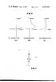
- FIG. 1is a cross-sectional of a PROM structure incorporated in the principles of the present invention.
- FIG. 2is a cross-section of the device of FIG. 1 during programming.
- FIG. 3is a cross-section of the device of FIG. 1 programmed into a low impedance state forming a PN diode.
- FIG. 4is a cross-section of the device of FIG. 1 programmed in the low impedance state having a PN junction forming a transistor.
- FIG. 5is a cross-section of the device of FIG. 1 programmed to the low impedance state forming a Schottky diode.
- FIGS. 6A, B, Care graphical illustrations of the voltage current curve for the different states of the device of FIG. 1.
- FIG. 7is a schematic of a circuit configuration using the device of FIG. 1.
- FIG. 1which illustrates the preferred embodiments of the storage cell of the present invention, shows a semiconductor substrate 10 with a semiconductor alloy layer 12 and an insulative layer 14 thereon.
- An amorphous semiconductor layer 16is formed on the alloy layer 12 and a portion of insulative layer 14 and a contact layer 18 is formed on the amorphous layer 16.
- the alloy layer 12 and the amorphous layer 16are semiconductor layers of the same semiconductor material as the substrate 10.
- the substrate 10is a single crystal silicon
- the alloy layer 12is palladium silicide
- amorphous layer 16is amorphous silicon
- the contact layer 18is aluminum.
- the structure of FIG. 1basically forms an amorphous silicon switch which is capable of being programmed from the high impedance states illustrated therein to a low impedance state.
- the mechanism used to program the amorphous layer 16is the SPEG mechanism described in the Pretorius et al article.
- a high voltage, depending upon the thickness of the amorphous silicon layer 16,is impressed between the contact layer 18 and the substrate 10.
- a hot channel 20develops therein as illustrated in FIG. 2 and the amorphous layer in the hot channel goes through a negative resistance transition as illustrated in FIGS. 6A and B.
- the temperature developed in the hot channelis between 400 and 1200 degrees centigrade.
- the alloy layer of palladium silicide therebetweendisassociates and is transported through the hot channel of the amorphous layer. As the palladium is transported, a single crystal column is formed in the amorphous silicon by solid phase epitaxial growth.
- the substrate 10may be of a first conductivity type, for example, N-type and the amorphous layer is doped with impurities of a second conductivity type, for example, P-type.
- a single crystal column 22 formedprovides a PN junction diode between the column 22 and the substrate 10.
- the palladium silicide layer 12 below the column 22has been transported to the top of the element forming a palladium silicide contact 24 with the aluminum contact 18.
- a P type region 26may be formed in an N type substrate 10 and the amorphous layer may be doped with N type impurities to form a column 28 as illustrated in FIG. 4.
- the programmed state of FIG. 4will produce a transistor.
- the conductivity type of the substrate 10 and the amorphous layer 16may be the same, as illustrated in FIG. 5, producing the programmed column 30.
- the resistivity of the amorphous layer 16 and of the resulting single crystal column 30is sufficiently high that a Schottky barrier is formed between the column 30 and the palladium silicide contact 24.
- the conductivity type of the column 30is N type, the resistivity should be 0.1 ohm-centimeter and above.
- the formation of the structure of FIG. 1commences with the masking and delineation of the insulation layer 14 to define the location of the storage devices on substrate 10 and the formation of the palladium silicide layer 12 on the exposed portions of the substrate.
- the amorphous layer 16is applied by, for example, having appropriate conductivity type and concentration of impurities doped therein.
- Contact metal layer 18is formed, for example, by evaporation to complete the structure.
- the palladium silicide layer 12may be formed by applying a layer of palladium on the substrate 10 and subsequently forming the amorphous silicon layer 16 thereover. This structure is annealed at between 200 and 400 degrees centigrade such that the palladium reacts both with the substrate and the amorphous layer to form palladium silicide.
- the PROM of the present inventionuses the SPEG mechanism to create in a switchable amorphous layer a single crystal column.
- the SPEG mechanismto operate, (a) the substrate or first layer 10, the semiconductor alloy layer 12 and the amorphous semiconductor layer 16 must be of the same semiconductor material and preferably the first layer 10 be single crystal; (b) the free energy level of the amorphous layer must be sufficiently higher than the free energy level of the first layer; and (c) the amorphous layer must be capable of switching states and crystalizing.
- silicon and palladium silicideis an example of a working model.
- Other alloys and semiconductor materials capable of SPEGmay be used. Germanium with an appropriate alloy may be an alternative.
- the base layer 10has been described as a substrate, the base layer may be a layer of single crystal semiconductor material formed on a substrate.
- FIGS. 6A, B, and CThe characteristics of the switch of FIG. 1 is illustrated in FIGS. 6A, B, and C.
- the high impedance stageis illustrated in FIG. 6A. With the voltage impressed across the amorphous semiconductor layer, the layer goes through a negative resistance transition as illustrated in FIG. 6B and a hot conducting channel results.
- the solid-phase epitaxial growth of single crystal silicon amorphous siliconstops when all the amorphous silicon has been consumed and the silicide layer appears at the top of the amorphous device.
- FIG. 6CSchematic of the resulting structure, for example, of FIG. 3 is illustrated in FIG. 7 as a diode.
- the cross-sectional layer of the single crystalline column grown in the amorphous layeris a function of the voltage level and duration. Since the column represents an ON state, compared to the OFF state of no column in the amorphous layer, the resistance value of the column varies inversely to the cross-sectional area of the column. Thus the present device provides, with the variation of column cross-sectional area, a multiple storage level device. Since the column formed is nonreversible, the level of the ON state of the device progressively changes to what may be considered a more ON state. With this analog feature, a matrix of these devices can store greater than the two normal levels of storage as well as being further programmed after the store of the initial ON state. This offers greater flexibility then would of been previously available.
Landscapes
- Engineering & Computer Science (AREA)
- Computer Hardware Design (AREA)
- Chemical & Material Sciences (AREA)
- Crystallography & Structural Chemistry (AREA)
- Physics & Mathematics (AREA)
- Condensed Matter Physics & Semiconductors (AREA)
- General Physics & Mathematics (AREA)
- Manufacturing & Machinery (AREA)
- Microelectronics & Electronic Packaging (AREA)
- Power Engineering (AREA)
- Semiconductor Memories (AREA)
Abstract
Description
The present invention relates generally to memory devices and more specifically to a programmable read-only memory structure (PROM) and method of operation.
With the advent of the use of elements was switching devices and more specifically as a memory cell, interest was developed in the use of amorphous semiconductive layers as switching and memory elements. "Switching In Elemental Amorphous Semiconductors" by Charles Feldman and Kishin Moorjani, in the Journal of Non-Crystalline Solids 2, (1970), pages 82-90, reports the ability of amorphous forms of silicon and geranium to operate as switching devices equivalent to the semiconductor glasses. The incorporation of this principle as memory elements described in "Read-Only Store Memory Element" by M. H. Brodsky, R. C. Dockerty and K. Weiser, IBM Technical Disclosure Bulletin, Vol 13 No. 11, Apr. 11, 1971 on page 3223. The Brodsky et al disclosure increases the local temperature to a point where the diffusant or alloy material diffuses into and/or alloys with the amorphous film to create additional conductive paths in the silicon in addition to the crystallization of the amorhpous semiconductor. This disclosure produces a polycrystalline structure which is difficult to control so as to reproduce reliably because of the diffusing or alloy mechanism. Thus there exists a need to provide a structure and a mechanism which will allow the use of semiconductor amorphous films as reproducible memory storage elements in a read-only memory structure.
Recent research has shown that epitaxial layers of silicon can be grown on single-crystal silicon substrates from an amorphous silicon layer by means of a solid state reaction. This solid-phase epitaxial growth (SPEG) of silicon is reported in "Dissociation Mechanism For Solid-Phase Epitaxy of Silcion in the Si (100)/Pd2 Si/Si (amorphous) System"; R. Pretorius, Z. L. Liau, S. S. Lau and M. A. Nicolet, Applied Physics Letters, Vol. 29, No. 9, Nov. 1, 1976, Pages 598-600. The present invention uses the SPEG mechanism in a memory structure similar to that described by Brodsky et al to provide a memory element which is most reproducible because of the epitaxy and capable of storing multiple signal levels.
The memory cell of the present invention includes a single crystal semiconductor substrate, a first layer of a metallic alloy of the semiconductor material, a second doped amorphous layer of the semiconducted material and a contact layer on said amorphous layer. The memory element is programmed by applying a voltage across the substrate and the contact layer of a sufficient magnitude and duration to cause solid-phase epitaxial growth of a single crystal column in the amorphous layer between the substrate and the contact layer. The solid-phase epitaxial growth causes a portion of the alloy layer to be transferred from the interface between the substrate and the amorphous layer to the interface between the column and the contact layer. The cross-sectional area of the column is a function of the voltage applied and the duration such that the memory cell may store varying levels or states. Since the column structure is irreversible, the cross-sectional and consequently the stored level may only be increased once created. By proper selection of the alloy layer and the impurity conductivity type and concentration, various types of diode barriers are formed. If the amorphous layer and the substrate are of opposite conductivity type, the column formed will produce a PN junction with the substrate. If the substrate and the amorphous layer are of the same conductivity type, the impurity concentration in the amorphous layer and the alloy is selected to produce a Schottky barrier between the alloy layer and the single crystal column formed in the amorphous layer. A transistor may also be formed wherein a region is formed in the substrate of opposite conductivity type from the substrate and the amorphous layer is formed of the same conductivity type as the substrate on the opposite conductivity type region in the substrate. Preferrably, the substrate and amorphous layer are silicon and the alloy is palladium silicide.
An object of the present invention is to provide a programmable read-only memory using amorphous silicon and programmed into a single crystal structure.
Another object of the invention is to provide a programmable read-only memory using an amorphous semiconductor material which is programmed by solid-phase epitaxial growth.
A further object of the invention is to provide a programmable read-only memory which is capable of a plurality of states.
An even further object is to provide an amorphous PROM capable of integration with conventional silicon devices and technology.
A still further object is to provide an amorphous PROM capable of integration as matrices with driver and decoder circuits.
Other objects, advantages, and novel features of the invention will become apparent from the following detailed description of the invention when considered in conjunction with the accompanying drawings.
FIG. 1 is a cross-sectional of a PROM structure incorporated in the principles of the present invention.
FIG. 2 is a cross-section of the device of FIG. 1 during programming.
FIG. 3 is a cross-section of the device of FIG. 1 programmed into a low impedance state forming a PN diode.
FIG. 4 is a cross-section of the device of FIG. 1 programmed in the low impedance state having a PN junction forming a transistor.
FIG. 5 is a cross-section of the device of FIG. 1 programmed to the low impedance state forming a Schottky diode.
FIGS. 6A, B, C, are graphical illustrations of the voltage current curve for the different states of the device of FIG. 1.
FIG. 7 is a schematic of a circuit configuration using the device of FIG. 1.
FIG. 1, which illustrates the preferred embodiments of the storage cell of the present invention, shows asemiconductor substrate 10 with asemiconductor alloy layer 12 and aninsulative layer 14 thereon. Anamorphous semiconductor layer 16 is formed on thealloy layer 12 and a portion ofinsulative layer 14 and acontact layer 18 is formed on theamorphous layer 16. Thealloy layer 12 and theamorphous layer 16 are semiconductor layers of the same semiconductor material as thesubstrate 10. In the preferred embodiments, thesubstrate 10 is a single crystal silicon, thealloy layer 12 is palladium silicide,amorphous layer 16 is amorphous silicon and thecontact layer 18 is aluminum.
The structure of FIG. 1 basically forms an amorphous silicon switch which is capable of being programmed from the high impedance states illustrated therein to a low impedance state. The mechanism used to program theamorphous layer 16 is the SPEG mechanism described in the Pretorius et al article. A high voltage, depending upon the thickness of theamorphous silicon layer 16, is impressed between thecontact layer 18 and thesubstrate 10. Ahot channel 20 develops therein as illustrated in FIG. 2 and the amorphous layer in the hot channel goes through a negative resistance transition as illustrated in FIGS. 6A and B. The temperature developed in the hot channel is between 400 and 1200 degrees centigrade.
Because of the high free energy of the amorphous silicon compared to the silicon substrate, the alloy layer of palladium silicide therebetween disassociates and is transported through the hot channel of the amorphous layer. As the palladium is transported, a single crystal column is formed in the amorphous silicon by solid phase epitaxial growth.
As illustrated in FIG. 3, thesubstrate 10 may be of a first conductivity type, for example, N-type and the amorphous layer is doped with impurities of a second conductivity type, for example, P-type. Asingle crystal column 22 formed provides a PN junction diode between thecolumn 22 and thesubstrate 10. Thepalladium silicide layer 12 below thecolumn 22 has been transported to the top of the element forming apalladium silicide contact 24 with thealuminum contact 18. Alternatively, aP type region 26 may be formed in anN type substrate 10 and the amorphous layer may be doped with N type impurities to form acolumn 28 as illustrated in FIG. 4. Thus the programmed state of FIG. 4 will produce a transistor. Also the conductivity type of thesubstrate 10 and theamorphous layer 16 may be the same, as illustrated in FIG. 5, producing the programmedcolumn 30. The resistivity of theamorphous layer 16 and of the resultingsingle crystal column 30 is sufficiently high that a Schottky barrier is formed between thecolumn 30 and thepalladium silicide contact 24. For example, if the conductivity type of thecolumn 30 is N type, the resistivity should be 0.1 ohm-centimeter and above.
The formation of the structure of FIG. 1 commences with the masking and delineation of theinsulation layer 14 to define the location of the storage devices onsubstrate 10 and the formation of thepalladium silicide layer 12 on the exposed portions of the substrate. Theamorphous layer 16 is applied by, for example, having appropriate conductivity type and concentration of impurities doped therein. Contactmetal layer 18 is formed, for example, by evaporation to complete the structure. Thepalladium silicide layer 12 may be formed by applying a layer of palladium on thesubstrate 10 and subsequently forming theamorphous silicon layer 16 thereover. This structure is annealed at between 200 and 400 degrees centigrade such that the palladium reacts both with the substrate and the amorphous layer to form palladium silicide.
The PROM of the present invention uses the SPEG mechanism to create in a switchable amorphous layer a single crystal column. For the SPEG mechanism to operate, (a) the substrate orfirst layer 10, thesemiconductor alloy layer 12 and theamorphous semiconductor layer 16 must be of the same semiconductor material and preferably thefirst layer 10 be single crystal; (b) the free energy level of the amorphous layer must be sufficiently higher than the free energy level of the first layer; and (c) the amorphous layer must be capable of switching states and crystalizing. The use of silicon and palladium silicide is an example of a working model. Other alloys and semiconductor materials capable of SPEG may be used. Germanium with an appropriate alloy may be an alternative.
Although thebase layer 10 has been described as a substrate, the base layer may be a layer of single crystal semiconductor material formed on a substrate.
The characteristics of the switch of FIG. 1 is illustrated in FIGS. 6A, B, and C. The high impedance stage is illustrated in FIG. 6A. With the voltage impressed across the amorphous semiconductor layer, the layer goes through a negative resistance transition as illustrated in FIG. 6B and a hot conducting channel results. The solid-phase epitaxial growth of single crystal silicon amorphous silicon stops when all the amorphous silicon has been consumed and the silicide layer appears at the top of the amorphous device. The characteristic of the device with the column is illustrated in FIG. 6C. Schematic of the resulting structure, for example, of FIG. 3 is illustrated in FIG. 7 as a diode.
The cross-sectional layer of the single crystalline column grown in the amorphous layer is a function of the voltage level and duration. Since the column represents an ON state, compared to the OFF state of no column in the amorphous layer, the resistance value of the column varies inversely to the cross-sectional area of the column. Thus the present device provides, with the variation of column cross-sectional area, a multiple storage level device. Since the column formed is nonreversible, the level of the ON state of the device progressively changes to what may be considered a more ON state. With this analog feature, a matrix of these devices can store greater than the two normal levels of storage as well as being further programmed after the store of the initial ON state. This offers greater flexibility then would of been previously available.
From the preceding description of the preferred embodiments, it is evident that the objects of the invention are obtained in that a programmable read only memory is provided which is most reproducible using amorphous semiconductor storage element and programmed by solid-phase epitaxial growth. Although the invention has been described and illustrated in detail, it is to be clearly understood that the same is by way of illustration and example only and is not to be taken by way of limitation. The spirit and scope of this invention are to be limited only by the terms of the appended claims.
Claims (36)
1. A method of producing a PROM element comprising:
forming a palladium silicide layer on a single crystal silicon substrate;
forming a layer of amorphous silicon on said palladium silicide layer;
forming a contact layer on said amorphous layer; and
applying programming voltage across said contact and said substrate of sufficient magnitude and duration to cause solid-phase epitaxial growth in said amorphous layer of a column of single crystal silicon extending between said substrate and said contact layer.
2. The method of claim 1 wherein the voltage magnitude and duration is selected to determine the cross-sectional dimension of said column.
3. The method of claim 1 wherein the voltage magnitude is sufficiently large to create a temperature in the amorphous layer in the range of 400 to 1200 degrees centigrade.
4. The method of claim 1 wherein the solid-phase epitaxial growth is performed until a layer of palladium silicide is formed between the column and said contact.
5. The method of claim 1 wherein the substrate is of a first conductivity type and said amorphous layer is formed doped with impurities of said first conductivity type.
6. The method of claim 5 including forming a region in the surface of said substrate of a conductivity type opposite said first conductivity type to separate said substrate and the subsequently formed amorphous layer.
7. The method of claim 1 wherein the substrate is of a first conductivity type and said amorphous layer is formed doped with impurities of a conductivity opposite said first conductivity type.
8. A method of fabricating a read only memory comprising:
forming a plurality of discrete regions of palladium silicide on a single crystal silicon substrate;
forming a layer of amorphous silicon on each of said discrete regions of palladium silicide;
forming a contact layer on each of said amorphous silicon layers;
creating a current between said substrate and selected contacts of a sufficient magnitude and duration to cause a column of single crystal silicon to epitaxially grow through said amorphous layer between said substrate and said selected contacts.
9. The method according to claim 8 wherein said substrate is of a first conductivity type, said amorphous layer is formed doped with impurities of a conductivity type opposite said first conductivity type and said epitaxial growth produces a layer of palladium silicide between the selected contacts and the single crystal columns to form an ohmic contact and said single crystal comumn forms a PN junction with said substrate.
10. The method according to claim 8 wherein said substrate is a first conductivity type, said amorphous layer is formed doped with impurities of said first conductivity type, and said epitaxial growth produces a layer of palladium silicide between the selected contacts and the single crystal columns to form a Schottky diode.
11. The method according to claim 8 wherein said substrate is a first conductivity type and said amorphous layer is formed doped with impurities of said first conductivity type, including forming a plurality of regions of second conductivity type opposite said first conductivity type in said substrate, wherein said palladium silicide regions are formed on said second conductivity type regions, and wherein said column, said second conductivity type regions and said substrate forming a bipolar transistor.
12. A semiconductor structure comprising:
a substrate of single crystal silicon;
a first layer of palladium silicide on said substrate;
a second layer of doped amorphous silicon on said first layer;
a third layer of contact material on said second layer;
a column of doped single crystal silicon on said substrate surrounded laterally by said first and second layers; and
a fourth layer of palladium silicide between said column and said third layer.
13. The semiconductor structure according to claim 12 wherein said substrate is of a first conductivity type, said column is of a second conductivity type opposite said first conductivity type, and said semiconductor structure is a diode.
14. The semiconductor structure according to claim 12 wherein said substrate is of a first conductivity type, said column is of said first conductivity type, and said semiconductor structure is a Schottky diode formed by said column and said fourth layer.
15. The semiconductor structure according to claim 12 including a region of first conductivity type formed in said substrate between said substrate and said first layer and column, and wherein said substrate and said column are of a second conductivity type opposite said first conductivity type and said semiconductor structure is bipolar transistor formed by said substrate, said region and said column.
16. In a programmable read only memory including a substrate and a plurality of storage locations formed on said substrate having either a first or second logic state, including at least one storage location in each of said logic states;
each storage location having a first logic state comprising a first layer of palladium silicide on said substrate, a second layer of amorphous silicon on said first layer, and a third layer of contact material on said second layer; and
each storage location having a second logic state comprising a first, second and third layer as each of said storage locations having a first logic state, a column of doped single crystal silicon extending between said substrate and said third layer and laterally surrounded by said first and second layers, and a fourth layer of palladium silicide between said column and said third layer.
17. The read only memory according to claim 16 wherein said substrate and said column are of the same conductivity type.
18. The read only memory according to claim 16 wherein said column has an impurity concentration sufficiently low to form a Schottky barrier with said fourth layer.
19. The read only memory according to claim 16 wherein said column is of a conductivity type opposite said substrate forming a PN junction therewith.
20. The read only memory according to claim 16 wherein some of said columns have different cross-sectional areas representing discrete levels of the second logic state.
21. A method of programming a programable read only memory having a crystalline substrate of a semiconductor material, and a plurality of spaced storage locations on said substrate, each including an alloy layer of a metal and said semiconductor material on said substrate, an amorphous layer of said semiconductor material on said alloy layer and a contact layer on said amorphous layer comprising:
applying a voltage across said substrate and said contact layer for the location to be programmed of a sufficient magnitude and duration to cause solid-phase epitaxial growth in said amorphous layer of a crystalline column of said semiconductor material extending between said substrate and said contact layer.
22. The method of claim 21 wherein said solid-phase epitaxial growth is performed until a portion of said alloy layer is transferred from its interface with said substrate to an interface between said column and said contact layer.
23. The method of claim 22 wherein the amorphous layer is doped with impurities, the impurity conductivity type and concentration and the alloy are selected to produce a diode between said contact and said substrate in a programmed storage location.
24. The method of claim 23 wherein said amorphous material has sufficiently low impurity concentration and said alloy is selected to form Schottky barrier between said alloy and said column.
25. The method of claim 23 wherein said amorphous material is doped with impurities of a conductivity type opposite the conductivity type of the impurities of said substrate to form a PN junction with the substrate.
26. The method of claim 21 wherein said semiconductor material is single crystal silicon and said alloy is palladium silicide.
27. A method of fabricating and programming a PROM element comprising:
providing a layer of single crystal semiconductor material;
forming an alloy layer of a metal and said semiconductor material on said single crystal layer;
forming an amorphous layer of said semiconductor material on said alloy layer;
forming a contact layer on said amorphous layer; and
applying a programming voltage across said contact layer and said single crystal layer of sufficient magnitude and duration to cause solid-phase epitaxial growth in said amorphous layer of a column of single crystal semiconductor extending between said single crystal layer and said contact layer.
28. The method of claim 27 wherein the solid-phase epitaxial growth is performed until a layer of said alloy is formed between the column and said contact layer.
29. The method of claim 27 wherein said amorphous layer is capable of switching between a high resistance and low resistance state before said solid-phase epitaxial growth occurs.
30. The method of claim 29 wherein said semiconductor is silicon and said alloy is palladium silicide.
31. The method of claim 27 wherein said amorphous layer is doped with impurities and said column forms a junction barrier between said contact layer and said single crystal layer.
32. A semiconductor structure comprising:
a layer of single crystal semiconductor material;
a alloy layer of a metal and said semiconductor material;
a doped amorphous layer of said semiconductor material on said alloy layer;
a contact layer of contact material on said amorphous layer;
a doped single crystal column of said semiconductor material on said single crystal layer surrounded laterally by said alloy and amorphous layers; and
a layer of said alloy between said column and said contact layer.
33. The semiconductor structure of claim 32 wherein said semiconductor material is silicon and said alloy is palladium silicide.
34. In a programmable read only memory including a substrate of a semiconductor material and a plurality of storage locations formed on said substrate having either a first or second logic state, including at least one storage location in each of said logic states;
each storage location having a first logic state comprising a first layer of an alloy of metal and said semiconductor material on said substrate, a second layer of amorphous form of said semiconductor material on said first layer, and a third layer of contact material on said second layer; and
each storage location having a second logic state comprising a first, second and third layer as each of said storage locations having a first logic state, a column of doped single crystal form of said semiconductor material extending between said substrate and said third layer and laterally surrounded by said first and second layers, and a fourth layer of said alloy between said column and said third layer.
35. The read only memory according to claim 34 wherein some of said columns have different cross-sectional areas representing discrete levels of the second logic state.
36. The read only memory according to claim 34 wherein said semiconductor material is silicon and said alloy is palladium silicide.
Priority Applications (1)
| Application Number | Priority Date | Filing Date | Title |
|---|---|---|---|
| US05/893,930US4174521A (en) | 1978-04-06 | 1978-04-06 | PROM electrically written by solid phase epitaxy |
Applications Claiming Priority (1)
| Application Number | Priority Date | Filing Date | Title |
|---|---|---|---|
| US05/893,930US4174521A (en) | 1978-04-06 | 1978-04-06 | PROM electrically written by solid phase epitaxy |
Publications (1)
| Publication Number | Publication Date |
|---|---|
| US4174521Atrue US4174521A (en) | 1979-11-13 |
Family
ID=25402358
Family Applications (1)
| Application Number | Title | Priority Date | Filing Date |
|---|---|---|---|
| US05/893,930Expired - LifetimeUS4174521A (en) | 1978-04-06 | 1978-04-06 | PROM electrically written by solid phase epitaxy |
Country Status (1)
| Country | Link |
|---|---|
| US (1) | US4174521A (en) |
Cited By (56)
| Publication number | Priority date | Publication date | Assignee | Title |
|---|---|---|---|---|
| FR2472246A1 (en)* | 1979-12-13 | 1981-06-26 | Energy Conversion Devices Inc | PROGRAMMABLE CELL FOR PROGRAMMABLE ELECTRONIC NETWORKS |
| US4316209A (en)* | 1979-08-31 | 1982-02-16 | International Business Machines Corporation | Metal/silicon contact and methods of fabrication thereof |
| FR2493022A1 (en)* | 1980-10-28 | 1982-04-30 | Energy Conversion Devices Inc | PERFECTED PROGRAMMABLE CELL FOR PROGRAMMABLE ELECTRONIC ARRAYS |
| EP0068058A1 (en)* | 1981-06-25 | 1983-01-05 | International Business Machines Corporation | Electrically programmable read-only memory |
| US4398343A (en)* | 1980-05-26 | 1983-08-16 | Shunpei Yamazaki | Method of making semi-amorphous semiconductor device |
| US4433342A (en)* | 1981-04-06 | 1984-02-21 | Harris Corporation | Amorphous switching device with residual crystallization retardation |
| US4462088A (en)* | 1981-11-03 | 1984-07-24 | International Business Machines Corporation | Array design using a four state cell for double density |
| US4569121A (en)* | 1983-03-07 | 1986-02-11 | Signetics Corporation | Method of fabricating a programmable read-only memory cell incorporating an antifuse utilizing deposition of amorphous semiconductor layer |
| US4590589A (en)* | 1982-12-21 | 1986-05-20 | Zoran Corporation | Electrically programmable read only memory |
| US4646266A (en)* | 1984-09-28 | 1987-02-24 | Energy Conversion Devices, Inc. | Programmable semiconductor structures and methods for using the same |
| US4670970A (en)* | 1985-04-12 | 1987-06-09 | Harris Corporation | Method for making a programmable vertical silicide fuse |
| US4835118A (en)* | 1986-09-08 | 1989-05-30 | Inmos Corporation | Non-destructive energy beam activated conductive links |
| US4847732A (en)* | 1983-09-15 | 1989-07-11 | Mosaic Systems, Inc. | Wafer and method of making same |
| US4876220A (en)* | 1986-05-16 | 1989-10-24 | Actel Corporation | Method of making programmable low impedance interconnect diode element |
| EP0365932A1 (en)* | 1988-10-14 | 1990-05-02 | Seiko Epson Corporation | Semiconductor device |
| US5409853A (en)* | 1994-05-20 | 1995-04-25 | International Business Machines Corporation | Process of making silicided contacts for semiconductor devices |
| US5502315A (en)* | 1989-09-07 | 1996-03-26 | Quicklogic Corporation | Electrically programmable interconnect structure having a PECVD amorphous silicon element |
| US5723358A (en)* | 1996-04-29 | 1998-03-03 | Vlsi Technology, Inc. | Method of manufacturing amorphous silicon antifuse structures |
| US5751012A (en)* | 1995-06-07 | 1998-05-12 | Micron Technology, Inc. | Polysilicon pillar diode for use in a non-volatile memory cell |
| US5753947A (en)* | 1995-01-20 | 1998-05-19 | Micron Technology, Inc. | Very high-density DRAM cell structure and method for fabricating it |
| US5753540A (en)* | 1996-08-20 | 1998-05-19 | Vlsi Technology, Inc. | Apparatus and method for programming antifuse structures |
| US5764563A (en)* | 1996-09-30 | 1998-06-09 | Vlsi Technology, Inc. | Thin film load structure |
| US5780919A (en)* | 1989-09-07 | 1998-07-14 | Quicklogic Corporation | Electrically programmable interconnect structure having a PECVD amorphous silicon element |
| US5783467A (en)* | 1995-12-29 | 1998-07-21 | Vlsi Technology, Inc. | Method of making antifuse structures using implantation of both neutral and dopant species |
| US5789795A (en)* | 1995-12-28 | 1998-08-04 | Vlsi Technology, Inc. | Methods and apparatus for fabricationg anti-fuse devices |
| US5789277A (en)* | 1996-07-22 | 1998-08-04 | Micron Technology, Inc. | Method of making chalogenide memory device |
| US5793094A (en)* | 1995-12-28 | 1998-08-11 | Vlsi Technology, Inc. | Methods for fabricating anti-fuse structures |
| US5812441A (en)* | 1996-10-21 | 1998-09-22 | Micron Technology, Inc. | MOS diode for use in a non-volatile memory cell |
| US5814527A (en)* | 1996-07-22 | 1998-09-29 | Micron Technology, Inc. | Method of making small pores defined by a disposable internal spacer for use in chalcogenide memories |
| US5831276A (en)* | 1995-06-07 | 1998-11-03 | Micron Technology, Inc. | Three-dimensional container diode for use with multi-state material in a non-volatile memory cell |
| US5837564A (en)* | 1995-11-01 | 1998-11-17 | Micron Technology, Inc. | Method for optimal crystallization to obtain high electrical performance from chalcogenides |
| US5841150A (en)* | 1995-06-07 | 1998-11-24 | Micron Technology, Inc. | Stack/trench diode for use with a muti-state material in a non-volatile memory cell |
| US5869843A (en)* | 1995-06-07 | 1999-02-09 | Micron Technology, Inc. | Memory array having a multi-state element and method for forming such array or cells thereof |
| US5879955A (en)* | 1995-06-07 | 1999-03-09 | Micron Technology, Inc. | Method for fabricating an array of ultra-small pores for chalcogenide memory cells |
| US5899707A (en)* | 1996-08-20 | 1999-05-04 | Vlsi Technology, Inc. | Method for making doped antifuse structures |
| US5909049A (en)* | 1997-02-11 | 1999-06-01 | Actel Corporation | Antifuse programmed PROM cell |
| US5920788A (en)* | 1995-06-07 | 1999-07-06 | Micron Technology, Inc. | Chalcogenide memory cell with a plurality of chalcogenide electrodes |
| US5952671A (en)* | 1997-05-09 | 1999-09-14 | Micron Technology, Inc. | Small electrode for a chalcogenide switching device and method for fabricating same |
| US5970336A (en)* | 1996-08-22 | 1999-10-19 | Micron Technology, Inc. | Method of making memory cell incorporating a chalcogenide element |
| US5985698A (en)* | 1996-07-22 | 1999-11-16 | Micron Technology, Inc. | Fabrication of three dimensional container diode for use with multi-state material in a non-volatile memory cell |
| USRE36518E (en)* | 1992-06-23 | 2000-01-18 | Micron Technology, Inc. | Method for making electrical contact with an active area through sub-micron contact openings and a semiconductor device |
| US6015977A (en)* | 1997-01-28 | 2000-01-18 | Micron Technology, Inc. | Integrated circuit memory cell having a small active area and method of forming same |
| US6025220A (en)* | 1996-06-18 | 2000-02-15 | Micron Technology, Inc. | Method of forming a polysilicon diode and devices incorporating such diode |
| US6031287A (en)* | 1997-06-18 | 2000-02-29 | Micron Technology, Inc. | Contact structure and memory element incorporating the same |
| US6087689A (en)* | 1997-06-16 | 2000-07-11 | Micron Technology, Inc. | Memory cell having a reduced active area and a memory array incorporating the same |
| US6117720A (en)* | 1995-06-07 | 2000-09-12 | Micron Technology, Inc. | Method of making an integrated circuit electrode having a reduced contact area |
| US6337266B1 (en) | 1996-07-22 | 2002-01-08 | Micron Technology, Inc. | Small electrode for chalcogenide memories |
| US6404669B2 (en)* | 1997-08-20 | 2002-06-11 | Micron Technology, Inc. | Reduced leakage DRAM storage unit |
| US6440837B1 (en) | 2000-07-14 | 2002-08-27 | Micron Technology, Inc. | Method of forming a contact structure in a semiconductor device |
| US6461945B1 (en)* | 2000-06-22 | 2002-10-08 | Advanced Micro Devices, Inc. | Solid phase epitaxy process for manufacturing transistors having silicon/germanium channel regions |
| US6521502B1 (en) | 2000-08-07 | 2003-02-18 | Advanced Micro Devices, Inc. | Solid phase epitaxy activation process for source/drain junction extensions and halo regions |
| US6563156B2 (en) | 2001-03-15 | 2003-05-13 | Micron Technology, Inc. | Memory elements and methods for making same |
| US6670713B2 (en) | 1996-02-23 | 2003-12-30 | Micron Technology, Inc. | Method for forming conductors in semiconductor devices |
| US6743680B1 (en) | 2000-06-22 | 2004-06-01 | Advanced Micro Devices, Inc. | Process for manufacturing transistors having silicon/germanium channel regions |
| US20040113154A1 (en)* | 2002-12-13 | 2004-06-17 | Ilya Karpov | Isolating phase change memory devices |
| USRE40790E1 (en)* | 1992-06-23 | 2009-06-23 | Micron Technology, Inc. | Method for making electrical contact with an active area through sub-micron contact openings and a semiconductor device |
Citations (5)
| Publication number | Priority date | Publication date | Assignee | Title |
|---|---|---|---|---|
| US3413157A (en)* | 1965-10-21 | 1968-11-26 | Ibm | Solid state epitaxial growth of silicon by migration from a silicon-aluminum alloy deposit |
| US3525146A (en)* | 1965-12-11 | 1970-08-25 | Sanyo Electric Co | Method of making semiconductor devices having crystal extensions for leads |
| US3877049A (en)* | 1973-11-28 | 1975-04-08 | William D Buckley | Electrodes for amorphous semiconductor switch devices and method of making the same |
| US3918032A (en)* | 1974-12-05 | 1975-11-04 | Us Army | Amorphous semiconductor switch and memory with a crystallization-accelerating layer |
| US4012235A (en)* | 1975-04-04 | 1977-03-15 | California Institute Of Technology | Solid phase epitaxial growth |
- 1978
- 1978-04-06USUS05/893,930patent/US4174521A/ennot_activeExpired - Lifetime
Patent Citations (5)
| Publication number | Priority date | Publication date | Assignee | Title |
|---|---|---|---|---|
| US3413157A (en)* | 1965-10-21 | 1968-11-26 | Ibm | Solid state epitaxial growth of silicon by migration from a silicon-aluminum alloy deposit |
| US3525146A (en)* | 1965-12-11 | 1970-08-25 | Sanyo Electric Co | Method of making semiconductor devices having crystal extensions for leads |
| US3877049A (en)* | 1973-11-28 | 1975-04-08 | William D Buckley | Electrodes for amorphous semiconductor switch devices and method of making the same |
| US3918032A (en)* | 1974-12-05 | 1975-11-04 | Us Army | Amorphous semiconductor switch and memory with a crystallization-accelerating layer |
| US4012235A (en)* | 1975-04-04 | 1977-03-15 | California Institute Of Technology | Solid phase epitaxial growth |
Non-Patent Citations (3)
| Title |
|---|
| Brodsky et al., IBM Technical Disclosure Bulletin, vol. 13, No. 11, Apr. 1971, P3223.* |
| Feldman et al., Journal of Non-Crystalline Solids (2), (1970), pp. 82-90.* |
| Pretorius et al., Applied Physics Letters, vol. 29, No. 9, Nov. 1, 1976, pp. 598-600.* |
Cited By (131)
| Publication number | Priority date | Publication date | Assignee | Title |
|---|---|---|---|---|
| US4316209A (en)* | 1979-08-31 | 1982-02-16 | International Business Machines Corporation | Metal/silicon contact and methods of fabrication thereof |
| DE3046721A1 (en)* | 1979-12-13 | 1981-10-29 | Energy Conversion Devices, Inc., 48084 Troy, Mich. | PROGRAMMABLE CELL OR ELECTRONIC ARRANGEMENT |
| US4599705A (en)* | 1979-12-13 | 1986-07-08 | Energy Conversion Devices, Inc. | Programmable cell for use in programmable electronic arrays |
| FR2472246A1 (en)* | 1979-12-13 | 1981-06-26 | Energy Conversion Devices Inc | PROGRAMMABLE CELL FOR PROGRAMMABLE ELECTRONIC NETWORKS |
| US4398343A (en)* | 1980-05-26 | 1983-08-16 | Shunpei Yamazaki | Method of making semi-amorphous semiconductor device |
| US4499557A (en)* | 1980-10-28 | 1985-02-12 | Energy Conversion Devices, Inc. | Programmable cell for use in programmable electronic arrays |
| FR2493022A1 (en)* | 1980-10-28 | 1982-04-30 | Energy Conversion Devices Inc | PERFECTED PROGRAMMABLE CELL FOR PROGRAMMABLE ELECTRONIC ARRAYS |
| DE3141967A1 (en)* | 1980-10-28 | 1982-06-16 | Energy Conversion Devices, Inc., 48084 Troy, Mich. | PROGRAMMABLE STORAGE CELL |
| US4433342A (en)* | 1981-04-06 | 1984-02-21 | Harris Corporation | Amorphous switching device with residual crystallization retardation |
| US4488262A (en)* | 1981-06-25 | 1984-12-11 | International Business Machines Corporation | Electronically programmable read only memory |
| EP0068058A1 (en)* | 1981-06-25 | 1983-01-05 | International Business Machines Corporation | Electrically programmable read-only memory |
| US4462088A (en)* | 1981-11-03 | 1984-07-24 | International Business Machines Corporation | Array design using a four state cell for double density |
| EP0078439A3 (en)* | 1981-11-03 | 1984-10-03 | International Business Machines Corporation | Read only storage using a four state cell |
| US4590589A (en)* | 1982-12-21 | 1986-05-20 | Zoran Corporation | Electrically programmable read only memory |
| US4569121A (en)* | 1983-03-07 | 1986-02-11 | Signetics Corporation | Method of fabricating a programmable read-only memory cell incorporating an antifuse utilizing deposition of amorphous semiconductor layer |
| US4847732A (en)* | 1983-09-15 | 1989-07-11 | Mosaic Systems, Inc. | Wafer and method of making same |
| US4646266A (en)* | 1984-09-28 | 1987-02-24 | Energy Conversion Devices, Inc. | Programmable semiconductor structures and methods for using the same |
| US4670970A (en)* | 1985-04-12 | 1987-06-09 | Harris Corporation | Method for making a programmable vertical silicide fuse |
| US4876220A (en)* | 1986-05-16 | 1989-10-24 | Actel Corporation | Method of making programmable low impedance interconnect diode element |
| US4835118A (en)* | 1986-09-08 | 1989-05-30 | Inmos Corporation | Non-destructive energy beam activated conductive links |
| EP0365932A1 (en)* | 1988-10-14 | 1990-05-02 | Seiko Epson Corporation | Semiconductor device |
| US5502315A (en)* | 1989-09-07 | 1996-03-26 | Quicklogic Corporation | Electrically programmable interconnect structure having a PECVD amorphous silicon element |
| US5717230A (en)* | 1989-09-07 | 1998-02-10 | Quicklogic Corporation | Field programmable gate array having reproducible metal-to-metal amorphous silicon antifuses |
| US6150199A (en)* | 1989-09-07 | 2000-11-21 | Quicklogic Corporation | Method for fabrication of programmable interconnect structure |
| US5989943A (en)* | 1989-09-07 | 1999-11-23 | Quicklogic Corporation | Method for fabrication of programmable interconnect structure |
| US5780919A (en)* | 1989-09-07 | 1998-07-14 | Quicklogic Corporation | Electrically programmable interconnect structure having a PECVD amorphous silicon element |
| USRE36518E (en)* | 1992-06-23 | 2000-01-18 | Micron Technology, Inc. | Method for making electrical contact with an active area through sub-micron contact openings and a semiconductor device |
| USRE40790E1 (en)* | 1992-06-23 | 2009-06-23 | Micron Technology, Inc. | Method for making electrical contact with an active area through sub-micron contact openings and a semiconductor device |
| US5409853A (en)* | 1994-05-20 | 1995-04-25 | International Business Machines Corporation | Process of making silicided contacts for semiconductor devices |
| US5753947A (en)* | 1995-01-20 | 1998-05-19 | Micron Technology, Inc. | Very high-density DRAM cell structure and method for fabricating it |
| US6096596A (en)* | 1995-01-20 | 2000-08-01 | Micron Technology Inc. | Very high-density DRAM cell structure and method for fabricating it |
| US20100184258A1 (en)* | 1995-06-07 | 2010-07-22 | Round Rock Research Llc | Method and apparatus for forming an integrated circuit electrode having a reduced contact area |
| US20010055874A1 (en)* | 1995-06-07 | 2001-12-27 | Fernando Gonzalez | Method for fabricating an array of ultra-small pores for chalcogenide memory cells |
| US7271440B2 (en) | 1995-06-07 | 2007-09-18 | Micron Technology, Inc. | Method and apparatus for forming an integrated circuit electrode having a reduced contact area |
| US20050029587A1 (en)* | 1995-06-07 | 2005-02-10 | Harshfield Steven T. | Method and apparatus for forming an integrated circuit electrode having a reduced contact area |
| US6831330B2 (en) | 1995-06-07 | 2004-12-14 | Micron Technology, Inc. | Method and apparatus for forming an integrated circuit electrode having a reduced contact area |
| US6797978B2 (en) | 1995-06-07 | 2004-09-28 | Micron Technology, Inc. | Method for fabricating an array of ultra-small pores for chalcogenide memory cells |
| US5831276A (en)* | 1995-06-07 | 1998-11-03 | Micron Technology, Inc. | Three-dimensional container diode for use with multi-state material in a non-volatile memory cell |
| US6077729A (en)* | 1995-06-07 | 2000-06-20 | Micron Technology, Inc. | Memory array having a multi-state element and method for forming such array or cellis thereof |
| US5841150A (en)* | 1995-06-07 | 1998-11-24 | Micron Technology, Inc. | Stack/trench diode for use with a muti-state material in a non-volatile memory cell |
| US5869843A (en)* | 1995-06-07 | 1999-02-09 | Micron Technology, Inc. | Memory array having a multi-state element and method for forming such array or cells thereof |
| US5879955A (en)* | 1995-06-07 | 1999-03-09 | Micron Technology, Inc. | Method for fabricating an array of ultra-small pores for chalcogenide memory cells |
| US20040161895A1 (en)* | 1995-06-07 | 2004-08-19 | Fernando Gonzalez | Method for fabricating an array of ultra-small pores for chalcogenide memory cells |
| US6653195B1 (en) | 1995-06-07 | 2003-11-25 | Micron Technology, Inc. | Fabrication of three dimensional container diode for use with multi-state material in a non-volatile memory cell |
| US6534780B1 (en) | 1995-06-07 | 2003-03-18 | Micron Technology, Inc. | Array of ultra-small pores for memory cells |
| US5920788A (en)* | 1995-06-07 | 1999-07-06 | Micron Technology, Inc. | Chalcogenide memory cell with a plurality of chalcogenide electrodes |
| US20020179896A1 (en)* | 1995-06-07 | 2002-12-05 | Harshfield Steven T. | Method and apparatus for forming an integrated circuit electrode having a reduced contact area |
| US6429449B1 (en) | 1995-06-07 | 2002-08-06 | Micron Technology, Inc. | Three-dimensional container diode for use with multi-state material in a non-volatile memory cell |
| US6420725B1 (en) | 1995-06-07 | 2002-07-16 | Micron Technology, Inc. | Method and apparatus for forming an integrated circuit electrode having a reduced contact area |
| US6391688B1 (en) | 1995-06-07 | 2002-05-21 | Micron Technology, Inc. | Method for fabricating an array of ultra-small pores for chalcogenide memory cells |
| US6916710B2 (en) | 1995-06-07 | 2005-07-12 | Micron Technology, Inc. | Method for fabricating an array of ultra-small pores for chalcogenide memory cells |
| US7687796B2 (en) | 1995-06-07 | 2010-03-30 | Micron Technology, Inc. | Method and apparatus for forming an integrated circuit electrode having a reduced contact area |
| US5751012A (en)* | 1995-06-07 | 1998-05-12 | Micron Technology, Inc. | Polysilicon pillar diode for use in a non-volatile memory cell |
| US6002140A (en)* | 1995-06-07 | 1999-12-14 | Micron Technology, Inc. | Method for fabricating an array of ultra-small pores for chalcogenide memory cells |
| US8017453B2 (en) | 1995-06-07 | 2011-09-13 | Round Rock Research, Llc | Method and apparatus for forming an integrated circuit electrode having a reduced contact area |
| US6117720A (en)* | 1995-06-07 | 2000-09-12 | Micron Technology, Inc. | Method of making an integrated circuit electrode having a reduced contact area |
| US6118135A (en)* | 1995-06-07 | 2000-09-12 | Micron Technology, Inc. | Three-dimensional container diode for use with multi-state material in a non-volatile memory cell |
| US6104038A (en)* | 1995-06-07 | 2000-08-15 | Micron Technology, Inc. | Method for fabricating an array of ultra-small pores for chalcogenide memory cells |
| US5837564A (en)* | 1995-11-01 | 1998-11-17 | Micron Technology, Inc. | Method for optimal crystallization to obtain high electrical performance from chalcogenides |
| US5793094A (en)* | 1995-12-28 | 1998-08-11 | Vlsi Technology, Inc. | Methods for fabricating anti-fuse structures |
| US5789795A (en)* | 1995-12-28 | 1998-08-04 | Vlsi Technology, Inc. | Methods and apparatus for fabricationg anti-fuse devices |
| US5783467A (en)* | 1995-12-29 | 1998-07-21 | Vlsi Technology, Inc. | Method of making antifuse structures using implantation of both neutral and dopant species |
| US5821558A (en)* | 1995-12-29 | 1998-10-13 | Vlsi Technology, Inc. | Antifuse structures |
| US6700211B2 (en) | 1996-02-23 | 2004-03-02 | Micron Technology, Inc. | Method for forming conductors in semiconductor devices |
| US6670713B2 (en) | 1996-02-23 | 2003-12-30 | Micron Technology, Inc. | Method for forming conductors in semiconductor devices |
| US5723358A (en)* | 1996-04-29 | 1998-03-03 | Vlsi Technology, Inc. | Method of manufacturing amorphous silicon antifuse structures |
| US5962911A (en)* | 1996-04-29 | 1999-10-05 | Vlsi Technology, Inc. | Semiconductor devices having amorphous silicon antifuse structures |
| US6229157B1 (en) | 1996-06-18 | 2001-05-08 | Micron Technology, Inc. | Method of forming a polysilicon diode and devices incorporating such diode |
| US6025220A (en)* | 1996-06-18 | 2000-02-15 | Micron Technology, Inc. | Method of forming a polysilicon diode and devices incorporating such diode |
| US6392913B1 (en) | 1996-06-18 | 2002-05-21 | Micron Technology, Inc. | Method of forming a polysilicon diode and devices incorporating such diode |
| US6337266B1 (en) | 1996-07-22 | 2002-01-08 | Micron Technology, Inc. | Small electrode for chalcogenide memories |
| US6111264A (en)* | 1996-07-22 | 2000-08-29 | Micron Technology, Inc. | Small pores defined by a disposable internal spacer for use in chalcogenide memories |
| US8264061B2 (en) | 1996-07-22 | 2012-09-11 | Round Rock Research, Llc | Phase change memory cell and devices containing same |
| US20110042640A1 (en)* | 1996-07-22 | 2011-02-24 | Round Rock Research, Llc | Method of fabricating phase change memory cell |
| US6316784B1 (en) | 1996-07-22 | 2001-11-13 | Micron Technology, Inc. | Method of making chalcogenide memory device |
| US5985698A (en)* | 1996-07-22 | 1999-11-16 | Micron Technology, Inc. | Fabrication of three dimensional container diode for use with multi-state material in a non-volatile memory cell |
| US7838416B2 (en) | 1996-07-22 | 2010-11-23 | Round Rock Research, Llc | Method of fabricating phase change memory cell |
| US6635951B1 (en) | 1996-07-22 | 2003-10-21 | Micron Technology, Inc. | Small electrode for chalcogenide memories |
| US20100151665A1 (en)* | 1996-07-22 | 2010-06-17 | Micron Technology, Inc | Small electrode for phase change memories |
| US7687881B2 (en) | 1996-07-22 | 2010-03-30 | Micron Technology, Inc. | Small electrode for phase change memories |
| US6797612B2 (en) | 1996-07-22 | 2004-09-28 | Micron Technology, Inc. | Method of fabricating a small electrode for chalcogenide memory cells |
| US5814527A (en)* | 1996-07-22 | 1998-09-29 | Micron Technology, Inc. | Method of making small pores defined by a disposable internal spacer for use in chalcogenide memories |
| US7494922B2 (en) | 1996-07-22 | 2009-02-24 | Micron Technology, Inc. | Small electrode for phase change memories |
| US20080048171A1 (en)* | 1996-07-22 | 2008-02-28 | Micron Technology, Inc. | Small electrode for phase change memories |
| US7273809B2 (en) | 1996-07-22 | 2007-09-25 | Micron Technology, Inc. | Method of fabricating a conductive path in a semiconductor device |
| US6492656B2 (en) | 1996-07-22 | 2002-12-10 | Micron Technology, Inc | Reduced mask chalcogenide memory |
| US5789277A (en)* | 1996-07-22 | 1998-08-04 | Micron Technology, Inc. | Method of making chalogenide memory device |
| US6531391B2 (en) | 1996-07-22 | 2003-03-11 | Micron Technology, Inc. | Method of fabricating a conductive path in a semiconductor device |
| US20050042862A1 (en)* | 1996-07-22 | 2005-02-24 | Zahorik Russell C. | Small electrode for chalcogenide memories |
| US5753540A (en)* | 1996-08-20 | 1998-05-19 | Vlsi Technology, Inc. | Apparatus and method for programming antifuse structures |
| US5899707A (en)* | 1996-08-20 | 1999-05-04 | Vlsi Technology, Inc. | Method for making doped antifuse structures |
| US6153890A (en)* | 1996-08-22 | 2000-11-28 | Micron Technology, Inc. | Memory cell incorporating a chalcogenide element |
| US5970336A (en)* | 1996-08-22 | 1999-10-19 | Micron Technology, Inc. | Method of making memory cell incorporating a chalcogenide element |
| US5998244A (en)* | 1996-08-22 | 1999-12-07 | Micron Technology, Inc. | Memory cell incorporating a chalcogenide element and method of making same |
| US5882997A (en)* | 1996-09-30 | 1999-03-16 | Vlsi Technology, Inc. | Method for making devices having thin load structures |
| US5764563A (en)* | 1996-09-30 | 1998-06-09 | Vlsi Technology, Inc. | Thin film load structure |
| US5978258A (en)* | 1996-10-21 | 1999-11-02 | Micron Technology, Inc. | MOS diode for use in a non-volatile memory cell background |
| US5812441A (en)* | 1996-10-21 | 1998-09-22 | Micron Technology, Inc. | MOS diode for use in a non-volatile memory cell |
| US6287919B1 (en) | 1997-01-28 | 2001-09-11 | Micron Technology, Inc. | Integrated circuit memory cell having a small active area and method of forming same |
| US6114713A (en)* | 1997-01-28 | 2000-09-05 | Zahorik; Russell C. | Integrated circuit memory cell having a small active area and method of forming same |
| US6534368B2 (en) | 1997-01-28 | 2003-03-18 | Micron Technology, Inc. | Integrated circuit memory cell having a small active area and method of forming same |
| US6015977A (en)* | 1997-01-28 | 2000-01-18 | Micron Technology, Inc. | Integrated circuit memory cell having a small active area and method of forming same |
| US5909049A (en)* | 1997-02-11 | 1999-06-01 | Actel Corporation | Antifuse programmed PROM cell |
| US20080055973A1 (en)* | 1997-05-09 | 2008-03-06 | Micron Technology Inc. | Small Electrode for a Chacogenide Switching Device and Method for Fabricating Same |
| US5952671A (en)* | 1997-05-09 | 1999-09-14 | Micron Technology, Inc. | Small electrode for a chalcogenide switching device and method for fabricating same |
| US20010002046A1 (en)* | 1997-05-09 | 2001-05-31 | Reinberg Alan R. | Small electrode for a chalcogenide switching device and method for fabricating same |
| US6189582B1 (en) | 1997-05-09 | 2001-02-20 | Micron Technology, Inc. | Small electrode for a chalcogenide switching device and method for fabricating same |
| US20060261380A1 (en)* | 1997-05-09 | 2006-11-23 | Reinberg Alan R | Small electrode for a chalcogenide switching device and method for fabricating same |
| US7453082B2 (en) | 1997-05-09 | 2008-11-18 | Micron Technology, Inc. | Small electrode for a chalcogenide switching device and method for fabricating same |
| US6777705B2 (en) | 1997-05-09 | 2004-08-17 | Micron Technology, Inc. | X-point memory cell |
| US6225142B1 (en) | 1997-06-16 | 2001-05-01 | Micron Technology, Inc. | Memory cell having a reduced active area and a memory array incorporating the same |
| US6087689A (en)* | 1997-06-16 | 2000-07-11 | Micron Technology, Inc. | Memory cell having a reduced active area and a memory array incorporating the same |
| US6252244B1 (en) | 1997-06-16 | 2001-06-26 | Micron Technology, Inc. | Memory cell having a reduced active area and a memory array incorporating the same |
| US6031287A (en)* | 1997-06-18 | 2000-02-29 | Micron Technology, Inc. | Contact structure and memory element incorporating the same |
| US6404669B2 (en)* | 1997-08-20 | 2002-06-11 | Micron Technology, Inc. | Reduced leakage DRAM storage unit |
| US6743680B1 (en) | 2000-06-22 | 2004-06-01 | Advanced Micro Devices, Inc. | Process for manufacturing transistors having silicon/germanium channel regions |
| US6461945B1 (en)* | 2000-06-22 | 2002-10-08 | Advanced Micro Devices, Inc. | Solid phase epitaxy process for manufacturing transistors having silicon/germanium channel regions |
| US8076783B2 (en) | 2000-07-14 | 2011-12-13 | Round Rock Research, Llc | Memory devices having contact features |
| US6440837B1 (en) | 2000-07-14 | 2002-08-27 | Micron Technology, Inc. | Method of forming a contact structure in a semiconductor device |
| USRE40842E1 (en)* | 2000-07-14 | 2009-07-14 | Micron Technology, Inc. | Memory elements and methods for making same |
| US20040124503A1 (en)* | 2000-07-14 | 2004-07-01 | Harshfield Steven T. | Memory elements and methods for making same |
| US20080017953A9 (en)* | 2000-07-14 | 2008-01-24 | Harshfield Steven T | Memory elements and methods for making same |
| US8786101B2 (en) | 2000-07-14 | 2014-07-22 | Round Rock Research, Llc | Contact structure in a memory device |
| US8362625B2 (en) | 2000-07-14 | 2013-01-29 | Round Rock Research, Llc | Contact structure in a memory device |
| US7504730B2 (en) | 2000-07-14 | 2009-03-17 | Micron Technology, Inc. | Memory elements |
| US20090152737A1 (en)* | 2000-07-14 | 2009-06-18 | Micron Technology, Inc. | Memory devices having contact features |
| US6607974B2 (en) | 2000-07-14 | 2003-08-19 | Micron Technology, Inc. | Method of forming a contact structure in a semiconductor device |
| US6521502B1 (en) | 2000-08-07 | 2003-02-18 | Advanced Micro Devices, Inc. | Solid phase epitaxy activation process for source/drain junction extensions and halo regions |
| US6563156B2 (en) | 2001-03-15 | 2003-05-13 | Micron Technology, Inc. | Memory elements and methods for making same |
| US7271403B2 (en)* | 2002-12-13 | 2007-09-18 | Intel Corporation | Isolating phase change memory devices |
| US20040113154A1 (en)* | 2002-12-13 | 2004-06-17 | Ilya Karpov | Isolating phase change memory devices |
Similar Documents
| Publication | Publication Date | Title |
|---|---|---|
| US4174521A (en) | PROM electrically written by solid phase epitaxy | |
| EP0072221B1 (en) | Non-volatile electrically programmable memory device | |
| US4312046A (en) | Vertical fuse and method of fabrication | |
| US4203123A (en) | Thin film memory device employing amorphous semiconductor materials | |
| US3877049A (en) | Electrodes for amorphous semiconductor switch devices and method of making the same | |
| US3171762A (en) | Method of forming an extremely small junction | |
| US3006791A (en) | Semiconductor devices | |
| US3699395A (en) | Semiconductor devices including fusible elements | |
| US3796926A (en) | Bistable resistance device which does not require forming | |
| US4677742A (en) | Electronic matrix arrays and method for making the same | |
| CA1155239A (en) | Diode and rom or eeprom device using same | |
| US5166901A (en) | Programmable memory cell structure including a refractory metal barrier layer | |
| GB2118365A (en) | A thin film MOS transistor and an active matrix liquid crystal display device | |
| US5093692A (en) | Tunnel diode detector for microwave frequency applications | |
| JPS5812742B2 (en) | semiconductor equipment | |
| US3983076A (en) | N-type amorphous semiconductor materials | |
| EP2162921B1 (en) | Junction diode with reduced reverse current | |
| SE451514B (en) | PROGRAMMABLE CELL CONSISTING OF AN AMORPH CELL BODY, AND NETWORK OF SUCH CELLS | |
| US4403399A (en) | Method of fabricating a vertical fuse utilizing epitaxial deposition and special masking | |
| US4196228A (en) | Fabrication of high resistivity semiconductor resistors by ion implanatation | |
| KR20070061053A (en) | Embedded phase change memory and its manufacturing method | |
| US4538167A (en) | Shorted junction type programmable read only memory semiconductor devices | |
| US4379005A (en) | Semiconductor device fabrication | |
| US4216489A (en) | MOS Dynamic memory in a diffusion current limited semiconductor structure | |
| US10833123B2 (en) | Phase change memory array with integrated polycrystalline diodes |