US4158218A - Ceramic capacitor device - Google Patents
Ceramic capacitor deviceDownload PDFInfo
- Publication number
- US4158218A US4158218AUS05/834,300US83430077AUS4158218AUS 4158218 AUS4158218 AUS 4158218AUS 83430077 AUS83430077 AUS 83430077AUS 4158218 AUS4158218 AUS 4158218A
- Authority
- US
- United States
- Prior art keywords
- ceramic chip
- intermediate portion
- chip
- ceramic
- metal foil
- Prior art date
- Legal status (The legal status is an assumption and is not a legal conclusion. Google has not performed a legal analysis and makes no representation as to the accuracy of the status listed.)
- Expired - Lifetime
Links
- 239000003985ceramic capacitorSubstances0.000titleclaimsabstractdescription9
- 239000000919ceramicSubstances0.000claimsabstractdescription52
- 239000000203mixtureSubstances0.000claimsabstractdescription24
- 239000011888foilSubstances0.000claimsabstractdescription16
- 239000003990capacitorSubstances0.000claimsdescription30
- 229910052751metalInorganic materials0.000claimsdescription23
- 239000002184metalSubstances0.000claimsdescription23
- 239000000758substrateSubstances0.000claimsdescription14
- 229910052709silverInorganic materials0.000claimsdescription13
- 229910000510noble metalInorganic materials0.000claimsdescription8
- 230000005489elastic deformationEffects0.000claimsdescription7
- 239000000470constituentSubstances0.000claimsdescription5
- 239000010953base metalSubstances0.000abstract1
- 230000035882stressEffects0.000description25
- 238000001465metallisationMethods0.000description12
- JRPBQTZRNDNNOP-UHFFFAOYSA-Nbarium titanateChemical compound[Ba+2].[Ba+2].[O-][Ti]([O-])([O-])[O-]JRPBQTZRNDNNOP-UHFFFAOYSA-N0.000description7
- 229910002113barium titanateInorganic materials0.000description7
- 239000000463materialSubstances0.000description7
- 238000000034methodMethods0.000description7
- BQCADISMDOOEFD-UHFFFAOYSA-NSilverChemical compound[Ag]BQCADISMDOOEFD-UHFFFAOYSA-N0.000description6
- 239000004332silverSubstances0.000description6
- BASFCYQUMIYNBI-UHFFFAOYSA-NplatinumChemical compound[Pt]BASFCYQUMIYNBI-UHFFFAOYSA-N0.000description5
- 229910018404Al2 O3Inorganic materials0.000description4
- GWEVSGVZZGPLCZ-UHFFFAOYSA-NTitan oxideChemical compoundO=[Ti]=OGWEVSGVZZGPLCZ-UHFFFAOYSA-N0.000description4
- KDLHZDBZIXYQEI-UHFFFAOYSA-NPalladiumChemical compound[Pd]KDLHZDBZIXYQEI-UHFFFAOYSA-N0.000description3
- YXFVVABEGXRONW-UHFFFAOYSA-NTolueneChemical compoundCC1=CC=CC=C1YXFVVABEGXRONW-UHFFFAOYSA-N0.000description3
- 229910045601alloyInorganic materials0.000description3
- 239000000956alloySubstances0.000description3
- 239000011152fibreglassSubstances0.000description3
- 238000010304firingMethods0.000description3
- 229910000765intermetallicInorganic materials0.000description3
- 229910052697platinumInorganic materials0.000description3
- -114×10-6 /° C.Inorganic materials0.000description2
- 239000003989dielectric materialSubstances0.000description2
- 238000009472formulationMethods0.000description2
- 239000011521glassSubstances0.000description2
- 229910052763palladiumInorganic materials0.000description2
- 229910001404rare earth metal oxideInorganic materials0.000description2
- 238000005245sinteringMethods0.000description2
- 229910000679solderInorganic materials0.000description2
- 239000007787solidSubstances0.000description2
- YBJHBAHKTGYVGT-ZKWXMUAHSA-N(+)-BiotinChemical compoundN1C(=O)N[C@@H]2[C@H](CCCCC(=O)O)SC[C@@H]21YBJHBAHKTGYVGT-ZKWXMUAHSA-N0.000description1
- 229910001316Ag alloyInorganic materials0.000description1
- PNEYBMLMFCGWSK-UHFFFAOYSA-Naluminium oxideInorganic materials[O-2].[O-2].[O-2].[Al+3].[Al+3]PNEYBMLMFCGWSK-UHFFFAOYSA-N0.000description1
- 229910052788bariumInorganic materials0.000description1
- DSAJWYNOEDNPEQ-UHFFFAOYSA-Nbarium atomChemical compound[Ba]DSAJWYNOEDNPEQ-UHFFFAOYSA-N0.000description1
- 125000000484butyl groupChemical group[H]C([*])([H])C([H])([H])C([H])([H])C([H])([H])[H]0.000description1
- 150000001875compoundsChemical class0.000description1
- 238000009792diffusion processMethods0.000description1
- 238000004090dissolutionMethods0.000description1
- 230000008030eliminationEffects0.000description1
- 238000003379elimination reactionMethods0.000description1
- PCHJSUWPFVWCPO-UHFFFAOYSA-NgoldChemical compound[Au]PCHJSUWPFVWCPO-UHFFFAOYSA-N0.000description1
- 229910052737goldInorganic materials0.000description1
- 239000010931goldSubstances0.000description1
- 238000009434installationMethods0.000description1
- 238000005259measurementMethods0.000description1
- 238000002844meltingMethods0.000description1
- 230000008018meltingEffects0.000description1
- 238000004806packaging method and processMethods0.000description1
- SWELZOZIOHGSPA-UHFFFAOYSA-Npalladium silverChemical compound[Pd].[Ag]SWELZOZIOHGSPA-UHFFFAOYSA-N0.000description1
- 239000002245particleSubstances0.000description1
- 230000000704physical effectEffects0.000description1
- HTYPUNPKBFMFFO-UHFFFAOYSA-Nplatinum silverChemical compound[Ag][Pt][Pt]HTYPUNPKBFMFFO-UHFFFAOYSA-N0.000description1
- 229910052573porcelainInorganic materials0.000description1
- 239000000843powderSubstances0.000description1
- 230000002000scavenging effectEffects0.000description1
- 238000000926separation methodMethods0.000description1
- 238000005476solderingMethods0.000description1
- 230000008646thermal stressEffects0.000description1
- FEPMHVLSLDOMQC-UHFFFAOYSA-Nvirginiamycin-S1Natural productsCC1OC(=O)C(C=2C=CC=CC=2)NC(=O)C2CC(=O)CCN2C(=O)C(CC=2C=CC=CC=2)N(C)C(=O)C2CCCN2C(=O)C(CC)NC(=O)C1NC(=O)C1=NC=CC=C1OFEPMHVLSLDOMQC-UHFFFAOYSA-N0.000description1
Images


Classifications
- H—ELECTRICITY
- H01—ELECTRIC ELEMENTS
- H01G—CAPACITORS; CAPACITORS, RECTIFIERS, DETECTORS, SWITCHING DEVICES, LIGHT-SENSITIVE OR TEMPERATURE-SENSITIVE DEVICES OF THE ELECTROLYTIC TYPE
- H01G2/00—Details of capacitors not covered by a single one of groups H01G4/00-H01G11/00
- H01G2/02—Mountings
- H01G2/06—Mountings specially adapted for mounting on a printed-circuit support
- H01G2/065—Mountings specially adapted for mounting on a printed-circuit support for surface mounting, e.g. chip capacitors
- H—ELECTRICITY
- H05—ELECTRIC TECHNIQUES NOT OTHERWISE PROVIDED FOR
- H05K—PRINTED CIRCUITS; CASINGS OR CONSTRUCTIONAL DETAILS OF ELECTRIC APPARATUS; MANUFACTURE OF ASSEMBLAGES OF ELECTRICAL COMPONENTS
- H05K3/00—Apparatus or processes for manufacturing printed circuits
- H05K3/30—Assembling printed circuits with electric components, e.g. with resistor
- H05K3/32—Assembling printed circuits with electric components, e.g. with resistor electrically connecting electric components or wires to printed circuits
- H05K3/34—Assembling printed circuits with electric components, e.g. with resistor electrically connecting electric components or wires to printed circuits by soldering
- H05K3/341—Surface mounted components
- H05K3/3421—Leaded components
- H05K3/3426—Leaded components characterised by the leads
- H—ELECTRICITY
- H01—ELECTRIC ELEMENTS
- H01F—MAGNETS; INDUCTANCES; TRANSFORMERS; SELECTION OF MATERIALS FOR THEIR MAGNETIC PROPERTIES
- H01F27/00—Details of transformers or inductances, in general
- H01F27/28—Coils; Windings; Conductive connections
- H01F27/29—Terminals; Tapping arrangements for signal inductances
- H01F27/292—Surface mounted devices
- H01F2027/295—Surface mounted devices with flexible terminals
- H—ELECTRICITY
- H05—ELECTRIC TECHNIQUES NOT OTHERWISE PROVIDED FOR
- H05K—PRINTED CIRCUITS; CASINGS OR CONSTRUCTIONAL DETAILS OF ELECTRIC APPARATUS; MANUFACTURE OF ASSEMBLAGES OF ELECTRICAL COMPONENTS
- H05K2201/00—Indexing scheme relating to printed circuits covered by H05K1/00
- H05K2201/10—Details of components or other objects attached to or integrated in a printed circuit board
- H05K2201/10613—Details of electrical connections of non-printed components, e.g. special leads
- H05K2201/10621—Components characterised by their electrical contacts
- H05K2201/10636—Leadless chip, e.g. chip capacitor or resistor
- H—ELECTRICITY
- H05—ELECTRIC TECHNIQUES NOT OTHERWISE PROVIDED FOR
- H05K—PRINTED CIRCUITS; CASINGS OR CONSTRUCTIONAL DETAILS OF ELECTRIC APPARATUS; MANUFACTURE OF ASSEMBLAGES OF ELECTRICAL COMPONENTS
- H05K2201/00—Indexing scheme relating to printed circuits covered by H05K1/00
- H05K2201/10—Details of components or other objects attached to or integrated in a printed circuit board
- H05K2201/10613—Details of electrical connections of non-printed components, e.g. special leads
- H05K2201/10742—Details of leads
- H05K2201/10886—Other details
- H05K2201/10909—Materials of terminal, e.g. of leads or electrodes of components
- H—ELECTRICITY
- H05—ELECTRIC TECHNIQUES NOT OTHERWISE PROVIDED FOR
- H05K—PRINTED CIRCUITS; CASINGS OR CONSTRUCTIONAL DETAILS OF ELECTRIC APPARATUS; MANUFACTURE OF ASSEMBLAGES OF ELECTRICAL COMPONENTS
- H05K2201/00—Indexing scheme relating to printed circuits covered by H05K1/00
- H05K2201/10—Details of components or other objects attached to or integrated in a printed circuit board
- H05K2201/10613—Details of electrical connections of non-printed components, e.g. special leads
- H05K2201/10742—Details of leads
- H05K2201/10886—Other details
- H05K2201/10924—Leads formed from a punched metal foil
- H—ELECTRICITY
- H05—ELECTRIC TECHNIQUES NOT OTHERWISE PROVIDED FOR
- H05K—PRINTED CIRCUITS; CASINGS OR CONSTRUCTIONAL DETAILS OF ELECTRIC APPARATUS; MANUFACTURE OF ASSEMBLAGES OF ELECTRICAL COMPONENTS
- H05K2201/00—Indexing scheme relating to printed circuits covered by H05K1/00
- H05K2201/10—Details of components or other objects attached to or integrated in a printed circuit board
- H05K2201/10613—Details of electrical connections of non-printed components, e.g. special leads
- H05K2201/10742—Details of leads
- H05K2201/10886—Other details
- H05K2201/10946—Leads attached onto leadless component after manufacturing the component
- H—ELECTRICITY
- H05—ELECTRIC TECHNIQUES NOT OTHERWISE PROVIDED FOR
- H05K—PRINTED CIRCUITS; CASINGS OR CONSTRUCTIONAL DETAILS OF ELECTRIC APPARATUS; MANUFACTURE OF ASSEMBLAGES OF ELECTRICAL COMPONENTS
- H05K2201/00—Indexing scheme relating to printed circuits covered by H05K1/00
- H05K2201/20—Details of printed circuits not provided for in H05K2201/01 - H05K2201/10
- H05K2201/2081—Compound repelling a metal, e.g. solder
- Y—GENERAL TAGGING OF NEW TECHNOLOGICAL DEVELOPMENTS; GENERAL TAGGING OF CROSS-SECTIONAL TECHNOLOGIES SPANNING OVER SEVERAL SECTIONS OF THE IPC; TECHNICAL SUBJECTS COVERED BY FORMER USPC CROSS-REFERENCE ART COLLECTIONS [XRACs] AND DIGESTS
- Y02—TECHNOLOGIES OR APPLICATIONS FOR MITIGATION OR ADAPTATION AGAINST CLIMATE CHANGE
- Y02P—CLIMATE CHANGE MITIGATION TECHNOLOGIES IN THE PRODUCTION OR PROCESSING OF GOODS
- Y02P70/00—Climate change mitigation technologies in the production process for final industrial or consumer products
- Y02P70/50—Manufacturing or production processes characterised by the final manufactured product
Definitions
- the present inventionis related to ceramic capacitors. More particularly, the present invention is directed to a ceramic capacitor device having a terminal arrangement which minimizes the stresses developed in the ceramic capacitor device by thermal expansion due to temperature variations occurring during utilization of the capacitor.
- Ceramic capacitorsi.e., monolithic ceramic chip capacitors are well known in the prior art; the making of a common type of multielectrode ceramic chip capacitor is described in U.S. Pat. No. 3,612,963--J. Piper et al.
- Ceramic chip capacitors in cubic shape, or other rectangular formare provided with metallizations at opposite end portions and these end metallizations are commonly attached to a circuit board or other substrate by terminal lead attachments.
- the capacitor deviceis subjected to wide temperature excursions, e.g., typically about 400° C., i.e., from about -55° C. to +345° C.
- a ceramic chip capacitoris formed of predominantly barium titanate or other material which has a coefficient of thermal expansion (CTE) which is considerably different from that of the usual circuit board substrate materials, e.g., Al 2 O 3 or fiberglass laminate. Consequently, attachment of a ceramic chip capacitor to such substrates will cause the ceramic chip to be subjected to substantial and varying stresses due to differential thermal expansion occurring during installation and use.
- CTEcoefficient of thermal expansion
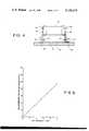
- FIGS. 1 and 2illustrate steps in the assembly of a capacitor device in accordance with the present invention
- FIGS. 3 and 4illustrate an embodiment of the present invention
- FIGS. 5 and 6are graphs illustrating dimensional and design relationships in accordance with the present invention.
- a ceramic capacitor device in accordance with the present inventioncomprises a ceramic chip having parallel opposed end surfaces, each end surface having a fired-on metallizing composition; a metal foil terminal strip bonded to each end surface solely by the fired-on metallizing composition, the metallizing composition having a metal constituent consisting essentially of at least 80% Ag and up to 20% noble metal and the metal foil terminal strips having a composition consisting essentially of at least 80% Ag and about 2 to 20% noble metal, each metal foil terminal strip having a first portion in close surface-to-surface contact and bonded to a respective end surface of the ceramic chip by the fired-on metallizing composition, an end portion remote from the ceramic chip and bent at substantially 90° with respect to the first portion, and an intermediate portion of predetermined length extending between the first portion and the end portion, the predetermined length being sufficient to permit elastic deformation of the intermediate portion during an ambient temperature excursion of 400° C. with the end portions fixed to a substrate having a TCE which is in the range of ⁇ 100% of the TCE of the ceramic chip,
- FIG. 1shows a conventional rectangularly shaped ceramic chip 10, e.g. predominantly barium titantate or predominantly a mixture of rare earth metal oxides with titania, having an unfired metallizing composition 12 containing finely divided particles of metal applied to the end portions of ceramic chip 10 including parallel opposed end surfaces 14 of ceramic chip 10.
- the metal constituent of metallizing composition 12consists essentially of at least about 80% by weight Ag and up to 20% by weight of noble metal, e.g. palladium, platinum or gold; preferred metal compositions are pure silver, 97% Ag+3% Pt, 80% Ag+20% Pd.
- a preferred form of metallization 12is a paste formed of a predominantly metal containing mixture of silver, palladium-silver or platinum-silver, glass frit and organics which, upon firing at about 850° C., provides a solid sintered metallization termination on a ceramic chip.
- a typical paste compositionis
- Ceramic chip 10 with unfired metallization paste 12is positioned above a terminal lead configuration indicated generally at 16 in FIG. 1 which has been conventionally formed from a foil strip 18.
- the ceramic chip 10Upon the lowering of chip 10 in the direction of arrows 20 the ceramic chip 10 is positioned as indicated in FIG. 2 with foil strips 22 closely contacting the unfired metallization 12 on opposed end faces 14. Chip 10 rests on horizontal tabs 24 which establish the predetermined length of intermediate portions 26 of strips 22.
- the metallization 12, and the end surface contacting portions of strips 22are conventionally subjected to a suitable metallization firing temperature, e.g. 750° C. to 850° C.
- the strip 18can now be cut along lines 32 to provide the capacitance device of the present invention illustrated in FIG. 3 having bent horizontal portions 34 which can be attached to suitable circuit board substrate as indicated in FIG. 4.
- right angle bent strip portions 34are conventionally affixed, e.g. by soldering to terminals 36, 38 of circuit board 40 which can be Al 2 O 3 , laminated fiberglass or other electrically insulative material suitable for such purpose.
- ceramic chip 10Upon being exposed to temperature excursions, ceramic chip 10 will undergo a thermal expansion different from that of substrate 40 in view of the known differences in CTE of barium titanate, 14 ⁇ 10 -6 /° C., and Al 2 O 3 7.8 ⁇ 10 -6 /° C., and fiberglass laminate 19 ⁇ 10 -6 /° C.
- a barium titanate ceramic chip rigidly attached to an Al 2 O 3 substratewill be subjected to a stress of about 9-10,000 psi for a 100° C. temperature excursion which can be calculated as follows following the procedure of Allen et al:
- This stressis in the range of the fracture stress of a barium titanate ceramic chip capacitor (9000-20,000 psi). Unless relieved, these forces can damage ceramic chip 10 leading to physical and electrical failure.
- these forcesare relieved by providing an intermediate "tab" portion 44 of strips 22 with at least a predetermined minimum length which enables elastic deformation of strips 22 in the directions indicated at 46 upon differential thermal expansion of chip 10 and substrate 40 during temperature excursions of from about -55° C. to +345° C.
- the length of intermediate strip portion, i.e. tab 44is selected also such that the forces 42 established at the end surfaces of ceramic chip 10 are not more than about 50% of the force that would be established if chip 10 were located such that intermediate tab portion 44 had a "0" length; i.e. chip 10 was rigidly secured to substrate 40 in a position in contact therewith as indicated at 10' in FIG. 4 without regard to the problem of differential thermal expansion.
- the following procedureillustrates the design of a tab 44 for a chip capacitor of arbitrary size.
- the stress reduction factor, Sis the ratio of actual stress 42 permitted in the tab-leaded capacitor to the stress induced in a chip capacitor of identical size rigidly attached to a substrate.
- Y**youngs Modulus for the ceramic chip.
- the procedureis general and may be used on any chip capacitor device, not all the physical properties data are available for all dielectrics.
- FIG. 5the relationship between the design factor, F, and the stress relief factor, S, using the above formula, is shown for those dielectrics for which physical constant data are readily available using silver as the tab material as described in, "Tab Lead Capacitor” op. cit.
- a stress reduction factor of 0.1corresponding to a 90% reduction in induced stress and hence, from FIG. 5, a design factor of 1.07 for a "BX" capacitor; (2) a chip capacitor measuring 0.225" in length from termination to termination, 0.245" in width transverse to the terminations and 0.050" in thickness (typical of a MIL-55681-designation CDR06BX474 capacitor chip); and (3) a silver-alloy tab as wide as the chip itself, 0.245".
- the graph of FIG. 6indicates, for example, that, if the tab intermediate portion 44 is 0.003 inches thick, then the length, h, of that portion must be 0.0144 inches to achieve the design criteria.
- the ceramic chip device in accordance with the present inventionhas several important advantages.
Landscapes
- Engineering & Computer Science (AREA)
- Power Engineering (AREA)
- Microelectronics & Electronic Packaging (AREA)
- Manufacturing & Machinery (AREA)
- Fixed Capacitors And Capacitor Manufacturing Machines (AREA)
Abstract
Description
Stress=Y capacitor (CTE.sub.cap -CTE.sub.substr.)·ΔT =16.10.sup.6 (14×10.sup.-6 -7.8×10.sup.-6)100=9900 psi
Claims (4)
Priority Applications (2)
| Application Number | Priority Date | Filing Date | Title |
|---|---|---|---|
| US05/834,300US4158218A (en) | 1977-09-19 | 1977-09-19 | Ceramic capacitor device |
| CA311,297ACA1104669A (en) | 1977-09-19 | 1978-09-14 | Ceramic capacitor device |
Applications Claiming Priority (1)
| Application Number | Priority Date | Filing Date | Title |
|---|---|---|---|
| US05/834,300US4158218A (en) | 1977-09-19 | 1977-09-19 | Ceramic capacitor device |
Publications (1)
| Publication Number | Publication Date |
|---|---|
| US4158218Atrue US4158218A (en) | 1979-06-12 |
Family
ID=25266612
Family Applications (1)
| Application Number | Title | Priority Date | Filing Date |
|---|---|---|---|
| US05/834,300Expired - LifetimeUS4158218A (en) | 1977-09-19 | 1977-09-19 | Ceramic capacitor device |
Country Status (2)
| Country | Link |
|---|---|
| US (1) | US4158218A (en) |
| CA (1) | CA1104669A (en) |
Cited By (29)
| Publication number | Priority date | Publication date | Assignee | Title |
|---|---|---|---|---|
| US4247883A (en)* | 1978-07-31 | 1981-01-27 | Sprague Electric Company | Encapsulated capacitor |
| US4455591A (en)* | 1982-02-03 | 1984-06-19 | Electronic Concepts, Inc. | Means and a method for converting finished electrical components with terminal leads to elements having planar terminations |
| EP0130386A1 (en)* | 1983-06-03 | 1985-01-09 | Wolfgang Westermann | Plastic foil-wound capacitor |
| US4571662A (en)* | 1983-06-17 | 1986-02-18 | Standard Telephones And Cables Plc | Leadless capacitors |
| US4581479A (en)* | 1984-11-16 | 1986-04-08 | Moore Theodore W | Dimensionally precise electronic component mount |
| US4617609A (en)* | 1984-04-03 | 1986-10-14 | Siemens Aktiengesellschaft | Electric capacitor in the form of a chip component and method for manufacturing same |
| US4660069A (en)* | 1983-12-08 | 1987-04-21 | Motorola, Inc. | Device with captivate chip capacitor devices and method of making the same |
| US4696082A (en)* | 1985-06-11 | 1987-09-29 | Compagnie Europeenne De Composants Electroniques Lcc | Method for manufacturing electrolytic capacitors and capacitors thus obtained |
| US4715118A (en)* | 1985-05-10 | 1987-12-29 | Compagnie Europeene De Composants Electroniques | Connecting strip for the manufacture of direct transfer electric components and manufacturing method for such components |
| US4811162A (en)* | 1987-04-27 | 1989-03-07 | Engelhard Corporation | Capacitor end termination composition and method of terminating |
| DE3924140A1 (en)* | 1988-07-26 | 1990-02-01 | Mitsubishi Mining & Cement Co | CHIP CAPACITOR WITH CONNECTIONS AND METHOD FOR THE PRODUCTION THEREOF |
| US5312581A (en)* | 1992-06-16 | 1994-05-17 | Rohm Co., Ltd. | Method for forming connector terminal electrodes of a lamination capacitor |
| US5903072A (en)* | 1997-03-21 | 1999-05-11 | Fasco Industries, Inc. | Electric motor input circuit with leadless capacitor assembly |
| EP1024507A1 (en)* | 1999-01-29 | 2000-08-02 | Murata Manufacturing Co., Ltd. | Ceramic electronic part |
| US6201683B1 (en)* | 1998-05-29 | 2001-03-13 | Murata Manufacturing Co., Ltd. | Ceramic electronic part and mounting structure for the same |
| US6438827B1 (en)* | 1997-07-23 | 2002-08-27 | Murata Manufacturing Co., Ltd. | Ceramic electronic part and method for producing the same |
| WO2005064228A3 (en)* | 2003-12-22 | 2006-03-23 | Matsushita Electric Works Ltd | Lighting device of discharge lamp, illumination apparatus and illumination system |
| US20090034155A1 (en)* | 2007-05-24 | 2009-02-05 | Daniel Devoe | Stacked multilayer capacitor |
| US20100053842A1 (en)* | 2007-05-24 | 2010-03-04 | Daniel Devoe | Stacked multilayer capacitor |
| US20100182732A1 (en)* | 2009-01-20 | 2010-07-22 | Tdk Corporation | Multilayer capacitor |
| US20100188798A1 (en)* | 2009-01-28 | 2010-07-29 | Tdk Corporation | Multilayer capacitor and method of manufacturing same |
| US20120043854A1 (en)* | 2008-06-02 | 2012-02-23 | Murata Manufacturing Co., Ltd. | Ceramic electronic component and method for manufacturing the same |
| WO2014012732A1 (en)* | 2012-07-17 | 2014-01-23 | Epcos Ag | Electrical component comprising a connection element having a plastic body |
| US20150114697A1 (en)* | 2013-10-29 | 2015-04-30 | Kemet Electronics Corporation | Ceramic Capacitors with Improved Lead Designs |
| WO2016058741A1 (en)* | 2014-10-14 | 2016-04-21 | Robert Bosch Gmbh | Electronic component having a connection element |
| US20170127524A1 (en)* | 2011-06-21 | 2017-05-04 | Schweizer Electronic Ag | Electronic Assembly Group and Method for Producing the Same |
| US20180350524A1 (en)* | 2017-05-30 | 2018-12-06 | Murata Manufacturing Co., Ltd. | Multilayer ceramic electronic component |
| US20210125781A1 (en)* | 2019-10-28 | 2021-04-29 | Tdk Corporation | Ceramic electronic device |
| US11456094B2 (en)* | 2020-03-03 | 2022-09-27 | Koa Corporation | Surface-mounted resistor |
Citations (6)
| Publication number | Priority date | Publication date | Assignee | Title |
|---|---|---|---|---|
| US1611183A (en)* | 1924-12-04 | 1926-12-21 | William H Frasse | Grid leak and condenser mounting |
| US3264534A (en)* | 1964-04-21 | 1966-08-02 | Vitramon Inc | Electrical component and thermal construction |
| US3345622A (en)* | 1964-01-10 | 1967-10-03 | Toko Inc | Mounting device for magnetic memory devices |
| US3585333A (en)* | 1969-06-30 | 1971-06-15 | Nat Tel Tronics Corp | Rapid assembly clip for mounting components on an electronic chassis |
| US3766451A (en)* | 1972-09-15 | 1973-10-16 | Trw Inc | Metallized capacitor with wire terminals |
| US4004200A (en)* | 1975-07-21 | 1977-01-18 | Johanson Manufacturing Corporation | Chip capacitor with spring-like leads |
- 1977
- 1977-09-19USUS05/834,300patent/US4158218A/ennot_activeExpired - Lifetime
- 1978
- 1978-09-14CACA311,297Apatent/CA1104669A/ennot_activeExpired
Patent Citations (6)
| Publication number | Priority date | Publication date | Assignee | Title |
|---|---|---|---|---|
| US1611183A (en)* | 1924-12-04 | 1926-12-21 | William H Frasse | Grid leak and condenser mounting |
| US3345622A (en)* | 1964-01-10 | 1967-10-03 | Toko Inc | Mounting device for magnetic memory devices |
| US3264534A (en)* | 1964-04-21 | 1966-08-02 | Vitramon Inc | Electrical component and thermal construction |
| US3585333A (en)* | 1969-06-30 | 1971-06-15 | Nat Tel Tronics Corp | Rapid assembly clip for mounting components on an electronic chassis |
| US3766451A (en)* | 1972-09-15 | 1973-10-16 | Trw Inc | Metallized capacitor with wire terminals |
| US4004200A (en)* | 1975-07-21 | 1977-01-18 | Johanson Manufacturing Corporation | Chip capacitor with spring-like leads |
Non-Patent Citations (1)
| Title |
|---|
| IBM Tech. Disclosure Bulletin, vol. 10, No. 8, 1/68, p. 1248.* |
Cited By (51)
| Publication number | Priority date | Publication date | Assignee | Title |
|---|---|---|---|---|
| US4247883A (en)* | 1978-07-31 | 1981-01-27 | Sprague Electric Company | Encapsulated capacitor |
| US4455591A (en)* | 1982-02-03 | 1984-06-19 | Electronic Concepts, Inc. | Means and a method for converting finished electrical components with terminal leads to elements having planar terminations |
| EP0130386A1 (en)* | 1983-06-03 | 1985-01-09 | Wolfgang Westermann | Plastic foil-wound capacitor |
| US4578737A (en)* | 1983-06-03 | 1986-03-25 | Wolfgang Westermann | Synthetic resin film wound capacitor |
| US4571662A (en)* | 1983-06-17 | 1986-02-18 | Standard Telephones And Cables Plc | Leadless capacitors |
| US4660069A (en)* | 1983-12-08 | 1987-04-21 | Motorola, Inc. | Device with captivate chip capacitor devices and method of making the same |
| US4617609A (en)* | 1984-04-03 | 1986-10-14 | Siemens Aktiengesellschaft | Electric capacitor in the form of a chip component and method for manufacturing same |
| US4581479A (en)* | 1984-11-16 | 1986-04-08 | Moore Theodore W | Dimensionally precise electronic component mount |
| US4715118A (en)* | 1985-05-10 | 1987-12-29 | Compagnie Europeene De Composants Electroniques | Connecting strip for the manufacture of direct transfer electric components and manufacturing method for such components |
| US4696082A (en)* | 1985-06-11 | 1987-09-29 | Compagnie Europeenne De Composants Electroniques Lcc | Method for manufacturing electrolytic capacitors and capacitors thus obtained |
| US4811162A (en)* | 1987-04-27 | 1989-03-07 | Engelhard Corporation | Capacitor end termination composition and method of terminating |
| DE3924140A1 (en)* | 1988-07-26 | 1990-02-01 | Mitsubishi Mining & Cement Co | CHIP CAPACITOR WITH CONNECTIONS AND METHOD FOR THE PRODUCTION THEREOF |
| GB2221572A (en)* | 1988-07-26 | 1990-02-07 | Mitsubishi Mining & Cement Co | Lead type chip capacitor and process for producing the same |
| US5006953A (en)* | 1988-07-26 | 1991-04-09 | Mitsubishi Mining & Cement Co., Ltd. | Lead type chip capacitor and process for producing the same |
| GB2221572B (en)* | 1988-07-26 | 1993-03-24 | Mitsubishi Mining & Cement Co | Lead type chip capacitor and process for producing the same |
| US5312581A (en)* | 1992-06-16 | 1994-05-17 | Rohm Co., Ltd. | Method for forming connector terminal electrodes of a lamination capacitor |
| US5903072A (en)* | 1997-03-21 | 1999-05-11 | Fasco Industries, Inc. | Electric motor input circuit with leadless capacitor assembly |
| US6438827B1 (en)* | 1997-07-23 | 2002-08-27 | Murata Manufacturing Co., Ltd. | Ceramic electronic part and method for producing the same |
| US6201683B1 (en)* | 1998-05-29 | 2001-03-13 | Murata Manufacturing Co., Ltd. | Ceramic electronic part and mounting structure for the same |
| EP1024507A1 (en)* | 1999-01-29 | 2000-08-02 | Murata Manufacturing Co., Ltd. | Ceramic electronic part |
| US6518632B1 (en) | 1999-01-29 | 2003-02-11 | Murata Manufacturing Co., Ltd. | Ceramic electronic part |
| EP1916883A1 (en)* | 2003-12-22 | 2008-04-30 | Matsushita Electric Works, Ltd. | Lighting device of discharge lamp, illumination apparatus and illumination system |
| US20070103879A1 (en)* | 2003-12-22 | 2007-05-10 | Yasushi Kambara | Lighting device of discharge lamp, illumination apparatus and illimination system |
| EP1909541A1 (en)* | 2003-12-22 | 2008-04-09 | Matsushita Electric Works, Ltd. | Lighting device of discharge lamp, illumination apparatus and illumination system |
| WO2005064228A3 (en)* | 2003-12-22 | 2006-03-23 | Matsushita Electric Works Ltd | Lighting device of discharge lamp, illumination apparatus and illumination system |
| US7667975B2 (en) | 2003-12-22 | 2010-02-23 | Matsushita Electric Works, Ltd. | Lighting device of discharge lamp, illumination apparatus and illumination system |
| US20090034155A1 (en)* | 2007-05-24 | 2009-02-05 | Daniel Devoe | Stacked multilayer capacitor |
| US7633739B2 (en) | 2007-05-24 | 2009-12-15 | Daniel Devoe | Stacked multilayer capacitor |
| US20100053842A1 (en)* | 2007-05-24 | 2010-03-04 | Daniel Devoe | Stacked multilayer capacitor |
| US8289675B2 (en) | 2007-05-24 | 2012-10-16 | Daniel Devoe | Stacked multilayer capacitor |
| US9805865B2 (en)* | 2008-06-02 | 2017-10-31 | Murata Manufacturing Co., Ltd. | Ceramic electronic component and method for manufacturing the same |
| US20120043854A1 (en)* | 2008-06-02 | 2012-02-23 | Murata Manufacturing Co., Ltd. | Ceramic electronic component and method for manufacturing the same |
| US20100182732A1 (en)* | 2009-01-20 | 2010-07-22 | Tdk Corporation | Multilayer capacitor |
| US8223471B2 (en)* | 2009-01-20 | 2012-07-17 | Tdk Corporation | Multilayer capacitor |
| US20100188798A1 (en)* | 2009-01-28 | 2010-07-29 | Tdk Corporation | Multilayer capacitor and method of manufacturing same |
| US8315035B2 (en)* | 2009-01-28 | 2012-11-20 | Tdk Corporation | Multilayer capacitor and method of manufacturing same |
| US10154593B2 (en)* | 2011-06-21 | 2018-12-11 | Schweizer Electronic Ag | Electronic assembly group and method for producing the same |
| US20170127524A1 (en)* | 2011-06-21 | 2017-05-04 | Schweizer Electronic Ag | Electronic Assembly Group and Method for Producing the Same |
| WO2014012732A1 (en)* | 2012-07-17 | 2014-01-23 | Epcos Ag | Electrical component comprising a connection element having a plastic body |
| US9865394B2 (en) | 2012-07-17 | 2018-01-09 | Epcos Ag | Electrical component comprising a connection element having a plastic body |
| US20150114697A1 (en)* | 2013-10-29 | 2015-04-30 | Kemet Electronics Corporation | Ceramic Capacitors with Improved Lead Designs |
| US10056320B2 (en)* | 2013-10-29 | 2018-08-21 | Kemet Electronics Corporation | Ceramic capacitors with improved lead designs |
| CN106797701A (en)* | 2014-10-14 | 2017-05-31 | 罗伯特·博世有限公司 | Electronic devices with connecting elements |
| WO2016058741A1 (en)* | 2014-10-14 | 2016-04-21 | Robert Bosch Gmbh | Electronic component having a connection element |
| US10249435B2 (en) | 2014-10-14 | 2019-04-02 | Robert Bosch Gmbh | Electronic component having a connection element |
| CN106797701B (en)* | 2014-10-14 | 2019-04-12 | 罗伯特·博世有限公司 | The device of electronics with connecting element |
| US20180350524A1 (en)* | 2017-05-30 | 2018-12-06 | Murata Manufacturing Co., Ltd. | Multilayer ceramic electronic component |
| US10790092B2 (en)* | 2017-05-30 | 2020-09-29 | Murata Manufacturing Co., Ltd. | Multilayer ceramic electronic component |
| US20210125781A1 (en)* | 2019-10-28 | 2021-04-29 | Tdk Corporation | Ceramic electronic device |
| US11615920B2 (en)* | 2019-10-28 | 2023-03-28 | Tdk Corporation | Ceramic electronic device |
| US11456094B2 (en)* | 2020-03-03 | 2022-09-27 | Koa Corporation | Surface-mounted resistor |
Also Published As
| Publication number | Publication date |
|---|---|
| CA1104669A (en) | 1981-07-07 |
Similar Documents
| Publication | Publication Date | Title |
|---|---|---|
| US4158218A (en) | Ceramic capacitor device | |
| JP3376971B2 (en) | Ceramic electronic components | |
| US4074340A (en) | Trimmable monolithic capacitors | |
| US6523235B1 (en) | Method of manufacturing a ceramic capacitor | |
| US5105333A (en) | Temperature compensating ceramic dielectric | |
| JP3206735B2 (en) | Ceramic capacitors | |
| US6201683B1 (en) | Ceramic electronic part and mounting structure for the same | |
| US5652466A (en) | Package for a semiconductor element | |
| JPH09180957A (en) | Multilayer ceramic capacitors | |
| US3490055A (en) | Circuit structure with capacitor | |
| JPH08107039A (en) | Ceramic electronic component | |
| US6686828B2 (en) | High-temperature detector and method of producing the same | |
| JP2002203737A (en) | Laminated ceramic electronic parts and its manufacturing method | |
| US6373684B2 (en) | Ceramic electronic component having lead terminal | |
| JP3206736B2 (en) | Ceramic capacitors | |
| US5111356A (en) | Composite structure resistant to thermal shocks and application thereof to multiple-layer ceramic capacitors | |
| US6917509B1 (en) | Single layer capacitor with dissimilar metallizations | |
| JP3253028B2 (en) | External electrode forming method of multilayer ceramic capacitor | |
| JP2001274037A (en) | Ceramic electronic part | |
| JPH0312446B2 (en) | ||
| JP3785961B2 (en) | Ceramic electronic components | |
| JPH09120932A (en) | Laminated electronic component | |
| JP3401836B2 (en) | Conductive paste | |
| JP2963420B2 (en) | Square chip electronic components | |
| JP2584393B2 (en) | Method for manufacturing electric component having external terminal |
Legal Events
| Date | Code | Title | Description |
|---|---|---|---|
| AS | Assignment | Owner name:MORGAN GUARANTY TRUST COMPANY OF NEW YORK, AND MOR Free format text:MORTGAGE;ASSIGNORS:UNION CARBIDE CORPORATION, A CORP.,;STP CORPORATION, A CORP. OF DE.,;UNION CARBIDE AGRICULTURAL PRODUCTS CO., INC., A CORP. OF PA.,;AND OTHERS;REEL/FRAME:004547/0001 Effective date:19860106 | |
| AS | Assignment | Owner name:UNION CARBIDE CORPORATION, Free format text:RELEASED BY SECURED PARTY;ASSIGNOR:MORGAN BANK (DELAWARE) AS COLLATERAL AGENT;REEL/FRAME:004665/0131 Effective date:19860925 | |
| AS | Assignment | Owner name:KEMET ELECTRONICS CORPORATION, ROUTE 276 S.E., GRE Free format text:ASSIGNMENT OF ASSIGNORS INTEREST.;ASSIGNOR:UNION CARBIDE CORPORATION, A CORP. OF NY.;REEL/FRAME:004740/0733 Effective date:19870401 Owner name:KEMET ELECTRONICS CORPORATION,SOUTH CAROLINA Free format text:ASSIGNMENT OF ASSIGNORS INTEREST;ASSIGNOR:UNION CARBIDE CORPORATION, A CORP. OF NY.;REEL/FRAME:004740/0733 Effective date:19870401 | |
| AS | Assignment | Owner name:HELLER FINANCIAL, INC., A DE CORP. Free format text:SECURITY INTEREST;ASSIGNOR:KEMET ELECTRONICS CORPORATION, A CORP. OF DE;REEL/FRAME:005562/0154 Effective date:19901221 | |
| AS | Assignment | Owner name:HELLER FINANCIAL, INC., AS COLLATERAL AGENT, ILLIN Free format text:SECURITY INTEREST;ASSIGNOR:KEMET ELECTRONICS CORPORATION;REEL/FRAME:006608/0042 Effective date:19930630 | |
| AS | Assignment | Owner name:NATIONSBANK OF NORTH CAROLINA, N.A., AS AGENT, NOR Free format text:SECURITY INTEREST;ASSIGNOR:KEMET ELECTRONICS CORPORATION;REEL/FRAME:007089/0893 Effective date:19940719 | |
| AS | Assignment | Owner name:KEMET ELECTRONICS CORPORATION, SOUTH CAROLINA Free format text:RELEASE BY SECURED PARTY;ASSIGNOR:NATIONSBANK, N.A. (CAROLINAS), AS COLLATERAL AGENT;REEL/FRAME:007360/0276 Effective date:19950221 |