US4075691A - Communication control unit - Google Patents
Communication control unitDownload PDFInfo
- Publication number
- US4075691A US4075691AUS05/629,510US62951075AUS4075691AUS 4075691 AUS4075691 AUS 4075691AUS 62951075 AUS62951075 AUS 62951075AUS 4075691 AUS4075691 AUS 4075691A
- Authority
- US
- United States
- Prior art keywords
- data
- memory
- pcm
- address
- register
- Prior art date
- Legal status (The legal status is an assumption and is not a legal conclusion. Google has not performed a legal analysis and makes no representation as to the accuracy of the status listed.)
- Expired - Lifetime
Links
Images


Classifications
- G—PHYSICS
- G06—COMPUTING OR CALCULATING; COUNTING
- G06F—ELECTRIC DIGITAL DATA PROCESSING
- G06F13/00—Interconnection of, or transfer of information or other signals between, memories, input/output devices or central processing units
- G06F13/10—Program control for peripheral devices
- G06F13/12—Program control for peripheral devices using hardware independent of the central processor, e.g. channel or peripheral processor
- G06F13/124—Program control for peripheral devices using hardware independent of the central processor, e.g. channel or peripheral processor where hardware is a sequential transfer control unit, e.g. microprocessor, peripheral processor or state-machine
- G—PHYSICS
- G06—COMPUTING OR CALCULATING; COUNTING
- G06F—ELECTRIC DIGITAL DATA PROCESSING
- G06F13/00—Interconnection of, or transfer of information or other signals between, memories, input/output devices or central processing units
- G06F13/38—Information transfer, e.g. on bus
- G06F13/382—Information transfer, e.g. on bus using universal interface adapter
- G06F13/385—Information transfer, e.g. on bus using universal interface adapter for adaptation of a particular data processing system to different peripheral devices
Definitions
- This inventionrelates generally to digital computer on-line data management systems and, more particularly, to a communication control unit for facilitating effective communication between multiple peripheral devices employing different communication disciplines and the system's main memory.
- communication (or line) disciplinemay be defined as the set of rules or criteria governing the message format utilized by a particular peripheral device. Exemplary factors distinguishing one discipline from another involve, for example, synchronization, start and end of message sequence, message segment length, etc.
- Many different communication disciplineshave evolved which are now well-known amongst those skilled in the art. The following list comprises only a small portion of those disciplines which might be of interest in a typical on-line data management system:
- the present inventionis directed to a communication control unit capable of efficiently handling multiple communication disciplines and which can be easily and inexpensively modified to handle new communication disciplines.
- a communication control unitincluding a programmable control module (PCM) or microcomputer containing a read-only memory for storing a control program.
- the program stored in read-only memorytypically referred to as firmware, is structured in two levels.
- the first levelconsists of a control program which contains common and control routines that are used by all line disciplines.
- the second level of firmwarecontains all line discipline-dependent instructions associated with the processing of transmit or receive characters according to a particular communication discipline.
- the application-dependent programs in the second levelare used by all channels on the PCM data bus that communicate according to the line discipline represented by the instructions of these programs.
- the preferred embodiment of the invention disclosed hereinis the BR 1569 communication control unit manufactured by the Bunker Ramo Corporation, Electronic Systems Division, Westlake Village, California.
- a single CCUinterfaces up to thirty-two full duplex serial data communication channels to a computer system, such as the PDP 11 which is a widely-used computer system manufactured by Digital Equipment Corporation, Maynard, Massachusetts.
- the PDP 11is characterized by its so-called Unibus organization which enables the BR 1569 to operate with direct access to the PDP 11 main memory.
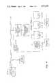
- FIG. 1is a block diagram of a data processing system incorporating a communication control unit in accordance with the present invention
- FIG. 2is a block diagram of the communications control unit of FIG. 1;
- FIG. 3is a block diagram of the direct memory access module (DMA) of FIGS. 1 and 2;
- DMAdirect memory access module
- FIG. 4is a block diagram of the programmable control module (PCM) of FIGS. 1 and 2;
- FIG. 5is a block diagram of the serial interface adaptor module (SIA) of FIGS. 1 and 2; and
- FIG. 6is a flow diagram depicting the firmware program processing.
- FIG. 1depicts in block form a PDP 11 data processing system incorporating a BR 1569 communication control unit (CCU) in accordance with the present invention.
- the PDP 11 systemis manufactured by Digital Equipment Corporation, Maynard, Massachusetts.
- the PDP 11 systemis illustrated in FIG. 1 as including a central processing unit (CPU), a data bus (Unibus), and a main memory.
- the BR 1569 CCUis manufactured by the Bunker Ramo Corporation, Westlake Village, California.
- the CCUis comprised of three major sections: (1) either one or two direct memory access modules (DMA) BR 1008; (2) either one or two programmable controller modules (PCM) BR 1003; and (3) one or more serial interface adaptors (SIA) BR 1086.
- DMAdirect memory access modules
- PCMprogrammable controller modules
- SIAserial interface adaptors
- the BR 1569comprises a direct memory access device that connects to the PDP 11 Unibus and, therefore, can receive data, address, and control signals from the Unibus and send data, address, and control signals to the Unibus. This permits the BR 1569 to receive and send data to the PDP 11 core memory in 16-bit words.
- the PCMis a programmable controller that receives and sends addresses, data, and commands from and to the DMA in 8-bit characters. After processing the data or commands, the PCM performs required functions and sends or receives the data or commands to or from the SIA via an 8-bit data bus.
- the SIAconverts the 8-bit character to serial data, after code conversion, if required, for transmission to the appropriate channel or receives the serial data and converts it to 8-bit characters with code conversion, if required, on receiving.
- Each SIAis coupled to four separate channels which may each connect to a peripheral device such as a CRT terminal, line printer, teletypewriter, etc.
- a single BR 1569can interface with up to thirty-two channels, for simplicity in explanation herein, the invention will be disclosed as a 16-channel CCU including one DMA and one PCM, as depicted in FIG. 1.
- the PCMperforms the necessary message framing and start and end of message tasks automatically thereby greatly alleviating the tasks normally required of the PDP 11 for communication.
- FIG. 2represents essentially the same structure as that illustrated in FIG. 1 except, however, it additionally shows the various interface signals between the Unibus, DMA, PCM, and SIA to thereby illustrate the basic functions performed by the communication control unit in accordance with the present invention.
- the DMAreceives the sixteen-bit data word from core memory.
- the BR 1569when the 1569 is receiving data from a peripheral device and needs to store data in core memory, the BR 1569 must provide:
- the DMAsends the sixteen-bit data word to core memory.
- each sixteen-bit Unibus wordis received by the DMA, it is buffered in memory in the PCM in eight-bit characters. At the same time, the characters are serially shifted out by the SIA.
- the DMAis then directed by the PCM to fetch another word from core via an NPR.
- the arbitration logic in the PDP 11 CPUgrants the Unibus to the BR 1569 and the DMA then places the address on the Unibus and receives the data word from core.
- FIG. 3illustrates a block diagram of the DMA module of FIGS. 1 and 2. Similar direct memory access modules are known in the art. The improvement in accordance with the present invention resides primarily in the PCM and its use in combination with the DMA and SIA to comprise a communication control unit capable of efficiently operating with multiple line disciplines.
- the DMA of FIG. 3includes a Unibus address interface and DMA module decode circuit group 100 which is comprised of the bus transceivers required to accept and present address information of the Unibus. Additionally, decoding logic is included for responding to a range of addresses applied to the Unibus. The addresses which activate the DMA are established with jumper wires added to the connector backplane. These are decoded by the DMA address patch block 102 and the channel address register patch block 104 in FIG. 3. The address is strapped into the backplane select active registers in the PCM plus a channel address register in the DMA.
- the DMAfurther includes a bus control module 106 which governs DMA data transfers.
- This control moduleresponds to non-processor requests (NPRs; a DMA data transfer function) generated by the RAM control unit 108.
- NPRsnon-processor requests
- Actions controlled on the Unibus by the bus control module 106are in master mode with the data source or datasink device operating as a slave.
- the bus control module 106primarily serves to provide the timing and necessary delays required to process NPR cycles.
- the bus control module 106applies a strobe line and a control line to the Unibus.
- the interrupt and channel address register block 110provides the hardware necessary for responding to interrupt commands initiated by the PCM.
- the interrupt operationconsists of requesting the Unibus via the bus acquisition module 116. Once bus acquisition is complete, an interrupt vector address is placed on the data lines simultaneous with the CPU bus interrupt signal. A block interrupt signal is presented to the PCM until it is cleared by the CPU reading the channel address register or else by the PCM pulsing the reset line. Interrupt vector addresses are strapped with the interrupt patch circuitry 112 represented in FIG. 3.
- Block 110includes a 6-bit channel address register which contains the contents of the select lines that were present when an interrupt occured. This register is a read-only register used by the CPU program to determine which device generated the last interrupt. When this register is read by the program, device interrupts are unblocked.
- the Unibus data interface block 114consists of the necessary transceivers required to accept 16 bits of data from the Unibus and apply data to the Unibus. Also included in this module is a 16-bit input data register. This register is used to trap bus data in order to allow releasing the Unibus while the data is being broken down into 8-bit characters.
- the Unibus acquisition module 116is used to gain control of the Unibus when either NPR or interrupt cycles are requested. This module will pass bus and NPR grants to down-line peripherals on the Unibus if either an NPR or interrupt request is pending.
- the RAM address counter/selector 118functions to apply a 10-bit address code to the PCM which selects specific hardware registers or locations in random access memory. Either the Unibus address or the device select code serves to define the address applied to the PCM. During direct memory access operations, the select lines are used as an address source whereas the CPU address lines are the source when registers in the PCM are directly accessed by the CPU. The CPU address lines may be applied directly to the PCM when accessing registers or these lines may be code converted to allow dispersion of the register addresses throughout the register allocation space on the Unibus. The bottom three bits of the RAM address counter/selector are used to address PCM registers under direction of the RAM control unit 108.
- RAM control unit 108includes a programmable read-only memory, a state counter, input selector, and instruction decoder.
- the basic function of the RAM control unitis to control the DMA transfers and CPU accesses of registers in the PCM. This will be discussed in greater detail hereinafter.
- controlsnecessary to reset the DMA circuits, initiate DMA operations, and report DMA bus, abort, and function completed status to the PCM.
- the buffer address register 120is a 24-bit register which contains the lower 16 bits of the Unibus address, 2 bits of extension address which define which 32,000-word block the buffer resides in, and 6 bits of temporary storage. Each of the three bytes which make up this register can be loaded independently by the RAM control unit 108. At the end of each DMA operation, the buffer address register is incremented by 2 with the exception of the upper 6 bits. The result of the increment may or may not be restored in a register contained in the PCM.
- the output data register 122is a 16-bit storage register used to buffer data to the Unibus. Each 8-bit byte of this register can be loaded independently by the RAM control unit 108 as 8-bit characters are received from the PCM. Outputs from the data register 122 are applied to the Unibus data receiver for application to the Unibus during DMA and register access cycles.
- the input data multiplexer 124serves to connect one of five data sources to the PCM. These data sources are:
- Source data to be applied to the PCM data busis selected by the RAM address counter 118 and the address interface 100.
- Data from the input data multiplexer 124is accompanied by a write command from the RAM control unit 108 under program control.
- the Unibus acquisition module 116gains control of the Unibus when either NPR or interrupt cycles are requested. This module 116 also will pass NPR and NPR bus grants to devices further down on the Unibus.
- the bus control module 106provides the timing and delays required to process NPR cycles. The sequence of control signals on the Unibus is as follows:
- the DMAissues a non-processor request (NPR).
- NPRnon-processor request
- the DMAissues a bus busy signal, followed by a master sync pulse and places the address on the address lines and data on the data lines (Data OUT only).
- Slave devicecore memory accepts the address and places the data on the data lines by executing a read cycle (Data IN) or strobes in data with a write cycle (Data OUT) and sending a store sync.
- Data INread cycle
- Data OUTwrite cycle
- the DMAaccepts the data (Data IN only), makes the bus not busy, and clears master sync.
- the Unibus data interface block 114contains a 16-bit buffer register and the necessary bus transceivers to accept and send data on the Unibus. Data is received or sent to the PCM in 8-bit characters. Data from the PCM is buffered in the data output register 122 into 16-bit words. Input data is transferred to the PCM via the input data multiplexer 124.
- the Unibus addressis stored in the buffer address register 120 which contains 24 bits to accommodate the 16-bit address plus the two extension bits and 6 command bits. On each word transferred, the DMA increments the address and the PCM increments the word count. Therefore, the input data multiplexer 124 multiplexes the input data bytes and the buffer address bytes under control of the RAM control unit 108 and the RAM address counter 118.
- the temporary data storage for data, address, status, etc. in the BR 1569is provided by the dual-ported random access memory in the PCM, to be discussed hereinafter.
- the RAM control unit 108 for one portis in the DMA module of FIG. 3. It is a programmable unit that can be tailored to meet the requirements of almost any type of controller.
- the RAM control unit 108contains a programmable read-only memory, state counter, input selector, and instruction decoder.
- the RAM control unit 108defines the following four states:
- RAMstore data in random access memory or read random access memory registers.
- the RAM control unit 108is capable of issuing 19 different instructions to the DMA control circuits as shown in table 1 hereinafter.
- the storing or reading of information in the random access memory in the PCMis under control of the RAM address counter 118 in the DMA.
- the RAM memory in the PCMis a dualported memory which is accessed by both DMA and PCM.
- Each channel addressis module 16 character addresses.
- the six 16-bit words associated with each channelare sorted in twelve 8-bit characters in RAM memory.
- Two additional charactershold the error conditions (one for the receive function and one for the transmit function) while two command characters allow the CPU to establish new-sync, enable interrupts or initialize the receiver or transmittor, in addition to holding the address extension bits.
- the RAM addressesrequire only 8 bits; 5 bits for channel address and 3 bits for temporary storage of data. However, 2 additional bits are provided. One bit is reserved for expansion and one bit for special discipline information.
- FIG. 4illustrates the programmable controller module (PCM) in significantly greater detail than its block representation FIGS. 1 and 2.
- the PCMis a small programmable parallel computer whose organization has been optimized for the communication control function in accordance with the invention herein.
- the PCMis comprised of a plurality of blocks or elements all of which communicate with each other via an internal data bus 200.
- Each of the PCM elementswill be described in detail hereinafter.
- the overall characteristics of the PCMwill be discussed and the instruction set considered.
- the PCMcomprises an efficient programmable parallel computer. It utilizes a data word length of 8 bits, while the instruction and address is 12 bits in length.
- the PCMis a microprogrammable processor with a single data bus and arithmetic register and a dual ported RAM memory.
- Variable datais stored in a 512-word (expandable) 8-bit RAM memory that is addressable by the PCM data source or the DMA.
- Program memoryis stored in a programmable read-only memory typically comprised of 2048 words by 12 bits.
- the microprogram instructionsare stored in a separate programmable read-only memory, as will be discussed.
- the arithmetic unitprovides the capability for the logical and arithmetic functions required.
- Instructions read from the ROM program memoryare executed in a maximum of three or four states, depending upon whether the RAM memory is addressed and the particular command as follows:
- the instructions for the PCMare listed in the following table 2. It will be noted that the instruction set is relatively simple and that the instructions basically comprise a single address command to RAM address pointers.
- the jump bit commandsare useful for testing flag conditions. In all jump commands, the jump address is in location N + 1. If no jump occurs, the address counter is incremented to address N + 2. There are 32 arithmetic commands and 16 logical commands as shown in table 3.
- microprogram instructionsare also 12 bits in length and have been selected to perform the normal hardware logic functions.
- the microprogram instructionsare contained in a separate read-only memory to be discussed more specifically hereinafter.
- PCMprogrammable read-only memory 202 consisting of 2048 12-bit words storing a sequence of instructions forming (1) control routines applicable to all peripheral devices and (2) character transmit/receive routines, each applicable to a particular communication discipline used by one or more of the connected peripheral devices.
- Instructions read out of the program memory 202are parallel loaded into the instruction register 204 at the beginning of each instruction execution cycle.
- the instruction register 204holds the instruction being executed by the PCM. Decoding and control of instruction execution is performed by the microprogram and control logic 206.
- the microprogram and control logic 206includes a 256 ⁇ 12 bit read-only memory which stores the microprogram.
- the microprogramgenerates/enables control register loading, address incrementing, memory writing, and command generation.
- the microprogramalso controls the arithmetic/logic unit and selects data sources.
- the inputs to the microprogramare the opcode part of the instruction (bits 8-11) in register 204, the bit condition selector, and the compare output of the arithmetic/logic unit.
- An edge triggered registeris used to synchronize the bit condition and compare inputs and to sequence through the states of the microprogram. Table 4 lists the outputs of the microprogram read-only memory and describes their function.
- the control logic in block 206consists of a four Megahertz clock generator, a power-on resetter initialize generator, multiplexors for data source selection and bit condition detection, decoders for register load signals and instruction execution enables, and a logic circuit to generate command pulses.
- the instructions read from the program memory 202are selected by address counter 208.
- the address counter 208is 12 bits in length allowing it to address an expanded program memory of 4096 words.
- the address counteris incremented each time the instruction register 204 is loaded and during a jump instruction if the specified condition is not satisfied.
- the address counter 208is parallel loaded during a jump instruction if the specified condition is satisfied.
- a power-on reset or an initializeclears the address counter to address zero.
- the PCMalso includes a random access memory 210 capable of storing 512 8-bit characters. Data is written into the memory during a transfer instruction in which one of its memory cells is defined as the data sink. Data is read from the memory during a transfer instruction in which one of its memory cells is defined as the data source.
- Memoryconsists of two sections, each section containing 256 8-bit characters. The sections consist of 1-bit ⁇ 256-bit random access memories operated in parallel to form an 8-bit ⁇ 256 character memory section. There is an external port into the memory 210 which can be used by the DMA, as aforementioned, to read or write into the memory 210 whenever the PCM is not using the memory 210.
- Accessing the memory 210is controlled by select register 212.
- the select registermay be used also to select a peripheral device to be serviced, via the SIA, by the PCM.
- the registeris loaded by means of a properly addressed load register or transfer function.
- the registermay be read by the PCM during a transfer instruction in which it is specified as the data source.
- the select registerspecifies the most significant 5 bits of the address of the random access memory.
- Output data register 214provides an output character which is to be read by the selected peripheral device, via the SIA.
- the selection of the device to read the output characteris made by the peripheral select register.
- the output data character registermay be loaded by means of a properly addressed load register or transfer instruction.
- the registermay not be used as a data source by a transfer function.
- An I/O commandis the means by which the PCM causes a function to be initiated in the selected peripheral device.
- the commandis generated by means of an I/O command instruction.
- the I/O command instructioncauses any combination of the 8 command bits to pulse true for 256 nanoseconds.
- the carry flag 216is set when a carry out occurs during execution of an arithmetic instruction.
- a jumpmay use the status of the carry flag as the jump condition.
- Arithmeticis performed by the arithmetic logic unit 218 and the accumulator register 220.
- the arithmetic logic unitcombines the contents of the accumulator and the specified data source according to the function specified by the instruction register contents. The results are placed in the accumulator register 220.
- the accumulator register 220is the primary operating register of the PCM. The results of all arithmetic and logic functions are placed in this register.
- the registermay be loaded by a properly addressed load register on transfer instruction. The register may be read during a transfer instruction in which it is specified as the data source. Jump instructions may compare the accumulator with instruction, RAM, input, or other register data.
- the PCMcontains two read-only memories, i.e., the program memory 202 and the microprogram memory 206.
- the microprogram in memory 206determines the instruction set of the PCM and may be changed to suit particular applications.
- the program memory 202stores the previously mentioned firmware which, as mentioned consists of two levels. It will be recalled that level 1 of the firmware contains control programs common to all communication disciplines and level 2 of the firmware contains discipline depending programs. A typical set of firmware will be discussed in detail hereinafter.
- each instruction loaded into register 204two, three, or four states of the microprogram are required depending upon the complexity of the function to be performed. As shown from the previously presented table 4, state zero is always used to load the instruction register 204 and increment address counter 208. The next state 1 is used for instruction decoding and to execute operations not requiring random access memory. During states two and three operations requiring random memory access may be executed.
- the firmware in the program memory 202enables the PCM to manipulate and transfer data between two or more devices, such as the PDP 11 core memory and a selected peripheral device.
- the select register 212provides the upper five bits of the RAM address for PCM instructions, thus a specific page of RAM is selected for each I/O device selected by the select register.
- an external devicemay read or write into the RAM at any address of its choice. If this device is the DMA, the RAM may be used to store computer memory addresses, word counts, or other parameters required for DMA data transfers and interrupt generation.
- This external port into the RAM memory 210allows the PDP 11 to load the RAM register or the BR 1569 to execute DMA transfers without interrupting the firmware.
- Data to be transferred from the PCM to a selected peripheral deviceis placed in the output data register 214. Then an I/O command is used to strobe the data into the device. Data to be transferred from a selected device to the PCM is loaded into the RAM memory 210 or a register by a transfer instruction. Then an I/O may be used to acknowledge the data transfer. I/O commands may be used to initiate control functions also. Device status may be monitored by the PCM at the input ports without transferring the status to a register.
- the DMAmay read the memory transfer address from the RAM memory 210 using the RAM DMA port when a read or write command is received from the PCM.
- the data to be read or writtenis stored in RAM. After the data transfer is completed, the DMA will update the memory transfer address and return it to the RAM memory.
- the PCMupdates and tests the word count.
- the DMAgenerates end of transfer interrupts when the PCM finds the word count equal to zero and sends a channel interrupt I/O command to the DMA.
- the DMAprovides status to the PCM using an input port.
- each channelis scanned sequentially by the PCM.
- High-speed channelsmay be scanned more frequently by performing a nonsequential or weighted scan.
- the time to scan a single channelis 8.06 microseconds.
- the time to test a characterdepends upon line protocol and the phase of the transmission cycle.
- Each linehas the following phases:
- Line syncmay be established by sending or receiving the following character sequence:
- ⁇is a pad character of all ones.
- each SIA modulecomprises a flexible serial communication interface providing a wide range of capabilities in terms of baud rates, communication modes, interface levels, character length, and code conversion.
- the basic function of the SIAis to convert parallel data to serial data for transmission data to a selected peripheral device and to convert serial data into parallel data on receiving information from a peripheral device.
- Each SIA modulecontains four full duplex communication channels.
- the SIA moduleincludes a PCM interface block 300 which functions to decode the PCM commands and select register addresses.
- the PCMcommands the SIA via an I/O command as shown in Table 2.
- the lower four bits of the commandare decoded as shown in Table 5.
- the PCM hereinis capable of interfacing with four SIA modules, only one of which is illustrated in FIG. 5. Since each SIA module provides four full duplex channels to peripheral devices, a PCM with four SIA modules coupled thereto can interface with 16 full duplex channels.
- the PCM interface module 300in addition to docoding PCM commands as depicted in the aforesaid fourth Table 5, also decodes channel select addresses as shown in the following Table 6.
- the sixth bitis used to denote code conversion if required, while the zero bit is used to specify transmission or receiving.
- the remaining four bitsare used to select one of four SIA modules and one of four channels on each SIA module.
- Datais set to the SIA output channels via I/O commands and transfer commands.
- the output datais sent to the multiplexor 302 which by-passes the code converter 304, if necessary.
- An X I/O commandloads this data into the transceiver 306.
- the input data channelis selected by the multiplexor 302, by-passes the code converter if necessary, and data is sent to the interface module 300 as an input to the PCM.
- the input data linesare buffed for four SIA modules. Therefore, no SIA places on the input lines until it has been addressed.
- Each SIA channelcan be interrogated to determine status.
- the definition of the status bitsare given in Table 7.
- the timer status bit in conjunction with bit 4is used to generate a sync-search pulse in synchronous operation, or the time between characters in asynchronous operation.
- the transmit data transfer request status bitrequests another character from the PCM for transmission. If the character is not received in time, the SIA generates idle fill characters for synchronous transmission, or marking bits for asynchronous transmission.
- the receive parity error bitindicates a receiving parity error.
- the overrun status bitindicates the transceiver received another character before the PCM accepted the previous character, which is indicated by a transfer acknowledge command from the PCM.
- the receive data transfer requestindicates to the PCM that the SIA has received another character.
- the carrier on status bitis typically a modem interface signal to indicate that the modem carrier is on and the clear to send status bit
- an alternate receive data transfer request status bitmay be used. This status bit immediately notifies the PCM that a character has been received without encountering scanning delays necessary for selection.
- Each SIA modulecontains a clock generator 308 which generates transmit and receive clocks by dividing down the frequency of a crystal oscillator (not shown).
- the code convertor 304consists of two read-only memories for transmit and two read-only memories for receive.
- the PCM data character or the SIA receive characteris used as an address to the ROM location which contains the converted character.
- Each SIA channelcontains a flag register 310 and time out circuitry that holds: request to send, new sync, disable sister channel, and sync search enable.
- Each SIA channelfurther contains line driver and receiver circuits 312 to interface with the required output or input characteristics of the peripheral devices to be connected to the SIA output channels.
- the foregoing descriptiongenerally defines the significant structural and functional aspects of the three primary sections of a preferred communication control unit (BR 1569) in accordance with the present invention.
- the three primary sectionsof course, being DMA, PCM, and SIA.
- DMAdigital versatile disc
- PCMdigital versatile machine
- SIAprogrammable programmable programmable programmable programmable programmable programmable programmable programmable programmable programmable programmable read-only memory
- SIAprogrammable programmable read-only memory
- the BR 1569is supported by device handler software that operates with the PDP 11 RXS-11D real time operating system for on-line operations.
- the BR 1569 device handleris independent of line disciplines and will control any number of channels, up to 128 full duplex mode.
- Each BR 1569 channelis assigned a unit number in the physical unit device table at system generation time.
- the device handleroperates as a priveledged task performing all input/output control for the BR 1569.
- Interface to user tasks and/or line discipline tasksis via the standard Queue I/O directive of RXS-11D.
- the form of the Queue I/O directive and a listing of the function code serviced by the device handlerare shown in Table 8 and 9.
- BR 1569 registersimplemented for each duplex channel and one register implemented for each group of 16 channels.
- the registersexist physically in the PCM RAM memory 210. However, they are addressed just as if they were in system core memory.
- the eight registers used for each channelare the:
- the receiver data registeris used to assemble received characters into computer words.
- the receiver buffer address registercontains the address of a message buffer in core memory.
- a buffer full conditionexists when the receiver word count register is incremented to zero. This condition is called an overflow of the word count register and initiates an interrupt of the central computer.
- the receiver command and status registeris used to control the receiver, to report the status of completed tasks, and contains bit 16 and 17 of the address contained in the receiver buffer address register. Receiver interrupts of the central computer are generated upon any of the following conditions, whichever occurs first:
- channel address registerIn addition to these eight registers per channel, there is a channel address register associated with each group of 16 channels. When a central computer interrupt is generated and control is transferred to the address specified in the address vector located at the interrupt vector address, the channel address register is accessed by the interrupt routine to determine which of the peripheral devices initiated the interrupt. With this information, the appropriate register set can then be addressed.
- This program or firmwareconstitutes the primary control element of the BR 1569 and consists of two levels of instructions; the first level instructions comprise a control program which contains routines common to all channels regardless of discipline, as well as a control program which is used by all disciplines and the second level contains all discipline dependent instructions associated with the processing of transmit or receive characters according to a particular communications discipline.
- the second level firmwaremay, for example, be partitioned into six different routines each for handling a different communication discipline.
- Typical communication disciplines known in the artare:
- a typical BR 1569has a greater number of channels than it has discipline dependent routines stored in firmware and thus in a typical application, peripheral devices on several channels will use the same discipline. For example only, in a typical application of a BR 1569, it may be necessary to couple a Remste Line Printer 300, a Visual Image Projection Terminal and several Teletypewriters to a PDP 11. The printer and terminal would, for example, operate in accordance with the RLP300 and VIP disciplines, respectively, and the Teletypewriter in accordance with ASCII TTY.
- Firmware for the BR 1569has been developed for a number of different disciplines and subsequently herein, the firmware for an exemplary discipline aforementioned ASCII TTY will be set forth along with the first level firmware containing the common routines.
- One of the primary purposes of utilizing a communications control unit in accordance with the inventionis to perform many of the tasks associated with servicing a peripheral device without requiring the intervention of the PDP 11 CPU.
- the BR 1569augments the throughput of the system by providing automatic message handling capabilities and data transfer prior to interrupting the central computer.
- Typical services performed by the firmwareare:
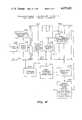
- FIG. 6shows the general processing flow for the firmware and the appendices hereto show the flow in considerably greater detail.
- Appendix A(1)comprises the instruction listings for the first firmware level and Appendix A(2) shows the corresponding flow chart.
- Appendix B(1)comprises the instruction listings for an exemplary routine in the second level of firmware, specifically relating to the communication discipline ASCII TTY, even parity.
- Appendix B(2)shows the corresponding flow chart.
- first level firmware processingis basically comprised of a START routine 400 and SCAN routine 402.
- START routine 400various initializing actions are taken prior to control passing to the SCAN routine.
- SCAN routinethe status of each channel is pulled and interrupts are serviced directly or by steering to the appropriate discipline dependent routine in firmware level 2. Interrupts are served in the following order:
- Execution of the first level of firmwarealso may involve some common receive and transmit routines which are the same for all disciplines. These routines set or clear status bits, store or save variable-type information in predefined random-access memory locations, and perform processes that are independent of line discipline requirements.
- Appendix A(1)first sets forth a list of "General Firmware Constant Definitions" and then on page 0006 the instruction sequence required for the initialization routine.
- the initialization proceduresinclude:
- Appendix A(1)next lists on page 0007 the instruction sequence of the SCAN routine.
- the scan routinefirst selects the channel which contains the last scan count used.
- the scan countis then code converted to the channel select to be scanned. If no code converter is present, a sequential scan is performed. If a code converter is present, the scan count is first converted to the select count, then the channel is scanned.
- interruptsare not enabled, no interrupts occurs and the interrupt pending bit is cleared.
- the SCAN routinecan cause a jump to an entry point in the second level of firmware by addressing one of the Line Discipline Entry Points defined on page 0004 of Appendix A(1).
- the common receiver and transmitter routine listingsbegin on pages 0010 and 0014 respectively.
- Appendix B(1)lists the instructions for a typical discipline dependent program; i.e., ASCII TTY. This instruction sequence can be entered as a consequence of a jump executed during the SCAN routine.
- the program represented by Appendix B(1)furnishes an interface on asynchronous channels to teletypewriters using ASCII coded characters. These characters can have odd or even parity and the program for even parity is shown.
- the message structures recognized by this firmwareare:
- Cr, etx, eot, dc4respectively identify a "carriage return", "end of text", "end of transmission” and "device control 4" character.
- the end-of-transmission interrupt of the central computeris generated on overflow of the word count register.
- the end-of-reception interrupt of the central computeris generated on reception of CR, ETX, EOT or DC4.
Landscapes
- Engineering & Computer Science (AREA)
- Theoretical Computer Science (AREA)
- Physics & Mathematics (AREA)
- General Engineering & Computer Science (AREA)
- General Physics & Mathematics (AREA)
- Computer Hardware Design (AREA)
- Microelectronics & Electronic Packaging (AREA)
- Microcomputers (AREA)
Abstract
Description
______________________________________ (1) VIP Visual Image Projection Terminal (Honeywell) (2) DN355 Datanet 355 (Honeywell) (3) Baudot TTY ITA Number Two Teletypewriter (4) ASCII TTY ASCII Teletypewriter - Odd or Even Parity (5) BISYC Point-to-Point Binary Synchronous Communications ______________________________________
TABLE 1 ______________________________________ DMA Interface Instruction SetOP Code Instruction 7 6 5 4 3 2 1 0 ______________________________________ No OP X X 0 0 0 0X X Load BAR 1X X 1 0 0 0X X Load BAR 2 X X 0 1 0 0X X Load BAR 3X X 1 1 0 0 X X Load DR1 X X 0 0 1 0 X XLoad DR2 X X 1 0 1 0 X X Func Cmp. X X 0 1 1 0 X XWrite RAM X X 1 1 1 0 X X Increment BAR X X 0 1 0 1 X XNPR Register X X 1 1 0 1 X X Reset RAM Address Counter X X 0 0 1 1 X X Load RAMAddress Counter X X 1 0 1 1 X X State Error X X 0 1 1 1 X X Issue SLAVE Sync X X X X X X 1 X IncrementRAM Address X X X X X X X 1 Counter Jump to ST 00 0 0 X X X X X X Jump to ST 01 1 0 X X X X X X Jump to ST 02 0 1 X X X X X X Jump to ST 03 1 1 X X X X X X Unassigned X X 0 0 0 1X X Unassigned X X 1 0 0 1X X Unassigned X X 1 1 1 1 X X ______________________________________ NOTE: X = Don't care; up to four instructions can be executed with one OP code (i.e., 1.sub.7 0100011.sub.0 = Jump to 01,Load BAR 1, issue SLAVE Sync, and Increment RAM Address Counter). BAR = Buffer Address Register. DR = Output Data Register.
______________________________________ Non-RAM State Instructions RAM Instructions ______________________________________ 0 Readinstruction Read instruction 1 Execute or set jump Addresssetting time condition 2 Execute jump Execute or setjump condition 3 Execute jump ______________________________________
TABLE 2 __________________________________________________________________________PCM Instruction Format Time Command OP Code msec __________________________________________________________________________ 11 10 9 8 7 6 5 4 3 2 1 0 Jump (A) ± (I.sub.8) 0 0 0 0 OPERAND 750 Jump (A)±(I.sub.8) 0 0 0 1 OPERAND 750 Load A 1 0 0 1 OPERAND 500 Load SR 1 0 1 0 OPERAND 500 Load ODR 1 0 1 1 OPERAND 500 ARITH with CIN 0 1 1 0 RAM Address ARITH Function 750 ARITH with CIN---- 0 1 1 1 RAM Address ARITH Function 750 Logical 1 0 0 0 RAM Address Logic Function 750 Uncond/Jump 0 1 0 1 Add:Input Port Upper 4 Bits of 500 or Register Jump Address Input/Output 1 1 0 0 DMA Commands SIA Commands 500 Transfer IP or 1 1 1 0 RAM Address Address Input 750 R to RAM Port or Register Jump RAM Bit = P 0 0 1 1 RAM Address P = 1 Address of 1000 0 Bit Position Jump IF IP or R = P 0 0 1 0 Address Input P = 1 Address of 750 Port or Register 0 Bit Position Jump Acc =, ± to 0 1 0 0 Address Input 1 = Not Used 750 (IP) or (R) Port or Register 0 ± Transfer (IP) or 1 1 0 1 Address Input 0 Add Sink 500 (SR) to Sink Register Port or Source Unused Register Register Transfer (RAM) 1 1 1 1 RAM Address 0 Add Sink 750 to Sink Register Unused Register __________________________________________________________________________ Note () = Content
TABLE 3 ______________________________________ Arithmetic Logic Instructions Arithmetic- Function Logic No Carry In Arithmetic-Carry In Code (φP 10) (φP 06) (φP 07) ______________________________________ 0000 A-- A A Plus 1 0001 A+B------A+B (A+B) Plus 1 0010 --AB A+B-- (A+B--) Plus 1 0011 0 Minus 1 (2's Compl.) 0 0100 AB---- A Plus AB-- A Plus AB--Plus 1 0101 B-- (A+B) Plus AB-- (A+B) Plus AB--Plus 1 0110 A⊕B A Minus B Minus 1 A Minus B 0111 AB-- AB--Minus 1 AB-- 1000 A--+B A Plus AB A Plus AB Plus 1 1001 A⊕B------ A Plus B A Plus B Plus 1 1010 B (A+B--) Plus AB (A+B--) Plus AB Plus 1 1011 AB AB Minus 1 AB 1100 1 Left Shift A Left Shift A/Carry In 1101 A+B-- (A+B) Plus A (A+B) Plus A Plus 1 1110 A+B (A+B--Plus A (A+B--) Plus A Plus 1 1111 A A Minus 1 A ______________________________________ A = Accumulator B = Contents of RAM Register (Sink) Code Input/Register (Source) Accumulator 02 Accumulator Select 03 Select Register - Bits 6, 7 are Zeros Output Data 04 Priority Bus 05 Serial Input Status 06 Serial Input Data 07 External (DMA) Status (7) - Bit 7 is Carry from Arithmetic Instruction 10 Zeros ______________________________________
TABLE 4 ______________________________________ Micro-ProgramInstructions 1. Enable Bits (Upper 4 bits) MNE- BI- MONICS NARY FUNCTION ______________________________________ A 0 0 0 0 No Operation B 0 0 0 1 Load Instruction Register and Increment Address C 0 0 1 0 Load Register (Specifyication by I.sub.L3) D 0 0 1 1 Increment Address E 0 1 0 0 Load Address with/(Data Source) (Indirect Jump) F 0 1 0 1 Load Address with/(Program ROM)(Jump) G 0 1 1 0 Load Accumulator. Set/Clear Carry Designator H 0 1 1 1 Load Accumulator I 1 0 0 0 Write intoRAM J 1 0 0 1 LoadSelect Register K 1 0 1 0 Load OutputData Register L 1 0 1 1 Initiate Command(s)M 1 1 0 0 Load External Register (Page-Memory Expand)N 1 1 0 1 Save Address (Subroutine Jump)O 1 1 1 0 Increment Pointer Counter. (Soubroutine Jump)P 1 1 1 1 Load Address from Push-Down Stack and Decrement Pointer Counter (Return from Subroutine) 2. A/L Mode Bits (Middle 4 bits) MNE- BI- MONICS NARY FUNCTION ______________________________________ C 0 1 1 0 Compare Accumulator toData Source L 1 0 0 1 Load Accumulator from Data Source AC- 0 1 0 0 Arithmetic - Not Carry In AD 0 0 0 0 Arithmetic - Carry InF 1 0 0 0 Logic Functions 3. Data Source Select (Bits 2.sup.2, 2.sup.3) MNE- MONICS 2.sup.3 2.sup.2 DESCRIPTION ______________________________________ L 0 0 Input/Register Specified by Instruction Bits 0→3 U 0 1 Input/Register Specified byInstruction Bits 4→7 I 1 0 Instruction (Lower 8 Bits)R 1 1 RAM (Address Specified by Select andInstruction Bits 4→7) 4. Next State (Bits 2.sup.1, 2.sup.0 STATE 2.sup.1 2.sup.0 COMMENTS ______________________________________ 0 0 0Read Instruction 1 0 1 Execute Non-RAM Instructions or SetNon-RAM Jump Condition 2 1 0 Execute RAM Instructions or RAM Jump or SetRAM Jump Condition 3 1 1 Execute RAM Jump ______________________________________
TABLE 5 ______________________________________ Command Bit Decoding Command Bit Definition ______________________________________ 3 2 1 0 1 1 1 1 Load Sync Detect character into selectedchannel 1 1 1 0 Load Control Word into selectedchannel 1 1 0 1 Restart Timer of selectedchannel 1 1 0 0 Reset Status Register of selectedchannel 1 0 1 1 Load Flag Register of selectedchannel 1 0 1 0 Load Transmitter Register of selectedchannel 1 0 0 1 Receive Transfer Acknowledge to selectedchannel 1 0 0 0 Load Idle Fill character into selected channel transmitter 0 X X X No Command to Decode ______________________________________
TABLE 6 ______________________________________ Channel Select Decoding Channel Select Bits Definition ______________________________________ 5 4 3 2 1 0 1 X X X X X Code convert selected channels data 0 X X X X X Perform nocode conversion X 1 1 X X X Select SIA Module No. 4 (channels 13-16)X 1 0 X X X Select SIA Module No. 3 (channels 9-12 X 0 1 X X X Select SIA Module No. 2 (channels 5-8) X 0 0 X X X Select SIA Module No. 1 (channels 1-4)X A B 1 1 X Select channel D of SIAModule AB X A B 1 0 X Select channel C of SIA Module AB X A B 0 1 X Select channel B of SIA Module AB X A B 0 0 X Select channel A of SIAModule AB X A B C D 1 Select transmit portion of channel CD of Module AB X A B C D 0 Select receive portion of channel CD of Module AB ______________________________________
TABLE 7 ______________________________________ Status Characters Status Character Bits Definition ______________________________________ 7 Selected channel time-out 6 Selected channel transmitdata transfer request 5 Select channel receiveparity error 4 Selected channelreceiver over-run error 3 Selected channel receivedata transfer request 2 Selected channelreceiver framing error 1 Selected channel carrier on 0 Selected channel clear to send ______________________________________
TABLE 8 ______________________________________ Queue I/O Directive Format Nord Byte Contents Meaning ______________________________________ 0 0 DIC Directive identification code for queue I/O 1 DPB Size Directive parameter block size inwords 1 Function Code See Table 4-12 2 Logical Unit Logical unit number assigned to achannel 3 0 Event flag # Event flag to set uponcompletion 1 Priority Priority ofrequest 4 Address of Address of a two-word status status block to be set upon completion of I/O orerror condition 5 AST Vector Asynchronous System Trap address to return control to uponcompletion 6Parameter 1 Buffer address of READ/ WRITE buffer (optional) 7Parameter 2 Buffer length in bytes (optional, even number) 8Parameter 3 STD address of task containing buffer (optional) ______________________________________
TABLE 9 ______________________________________ I/O Function Codes Serviced Function Code Meaning ______________________________________Kill 12 Kill all current I/O and requests for this task I/O Rundown 22 Same as Kill except done by EXEC to aborted tasks Unload 42 Complete all current requests, then exit the system (from EXEC only) Write 400 Output the specified buffer to the line specified by the logical unit number assignment Write/Resync 420 Resynchronize with crypto gear, then perform WRITE READ 1000 Set the specified input line buffer address and length to the address and length in1, 2, and 3 Read/New Sync 1020 Notify modem to expect new synchro- nization (for polling a new device) and then READ Attach 1400 Accept I/O commands for specified line from this task only Detach 2000 Release attached task from specified line Set Disable Bit 2410 Disable Redundant Channel (for BR-1569s running in parallel, stops transmission from other channel) Set Idle 2420 Start continuous idle synchronization Sync Bit of channel Set Both Bits 2430 Does both DISABLE and IDLE SYNC Reset Disable 3010 Enables redundant channel Bit Reset Idle Sync 3020 Stops continuous idle synchronization Bit Reset Both Bits 3030 Does both Enable and stop IDLE SYNC ______________________________________ parameters
______________________________________ COINS COMMUNITY ON-LINE INTEL. NET SERVICE VIP VISUAL IMAGE PROJECTION TERMINAL (HONEYWELL) DN355 DATA-NET 355 (HONEYWELL) BAUDOT TTY ITA No. 2 TELETYPEWRITER ASCII TTY ASCII TELETYPEWRITER - ODD OR EVEN PARITY PT-PT POINT-TO-POINT BISYNCH BINARY SYNCHRONOUS ASCII OR EBCDIC CHARACTER CHARACTER INTERFACE RLP300 REMOTE LINE PRINTER 300 (HONEYWELL)SYSTEM 1 UNIVAC 1652 TERMINAL GENSER AUTODIN GENERALSERVICE PORT SYSTEM 2COLLECTION SYSTEM 2 WUPTC WESTERN UNION PROGRAMMABLE TERMINAL CONTROLLER (AUTODIN) DN30 DATA-NET 30 (HONEYWELL) DACOM DACOM FACSIMILE UNIT 188C TTY MILITARY TELETYPEWRITER DP2910 DATA PRODUCTS 2910/MIL/TEMPEST LINE PRINTER D900A VERSATEC PRINTER/PLOTTER DDCMP DIGITAL EQUIPMENTCORPORATION DDCMP SYSTEM 3COLLECTION SYSTEM 3SYSTEM 4COLLECTION SYSTEM 4SYSTEM 5COLLECTION SYSTEM 5SYSTEM 6COLLECTION SYSTEM 6SYSTEM 7COLLECTION SYSTEM 7 ______________________________________
__________________________________________________________________________1569 Instruction Mnemonics __________________________________________________________________________0.75 ARC R0, F0 Arithmetic Functions with Carry In Result in Accumulator Register and RAM location R0 used as operands for function F0 (Table I). 0.75 ARN R3, F12 Arithmetic Functions Without Carry In (See above and Table I) 0.75 JAE Op, Addr Jump to Addr if contents of accumulator, (A) equals op. 0.75 JAN Op, Addr Jump to Addr if (A) ≠ Op (A) = Inp, for E=1 0.75 JIA Inp, E, Jump to Addr if (A) = Inp, for E=0 Addr. 0.75 JIE Inp, P, Jump to Addr if bit Z, 0-7, of Inp = Z, Addr Off = 0 P On = 1 0.5 JMP Inp, Addr Jump to Addr/Inp; Addr = upper 4 bits of jump address (Inp) = lower 8 bits of jump address 1.0 JRE RAM,P, Jump to Addr if bit Z, 0-7, of RAM Z, Addr location RAM = Off=0 P On -1 Logical functions, result in Accumulator (See Table I). 0.75 LGC R12, F17 Register and RAM location R12 used as operands for function F17. 0.5 LOA L Load Accumulator with literal L 0.5 LOO L Load Output Register with literal L 0.5 LOS L Load Select Register with literal L 0.75 TIR RAM, SOURCE Transfer data from input port SOURCE to RAM location RAM 0.5 TIS SOURCE, SINK Transfer data from SOURCE input port register to SINK register 0.75 TRS RAM, SINK Transfer data from RAM location RAM to selected register SINK 0.5 XIO CMD Execute I/O command. Each command line activated if the corresponding bit of CMD is on (bits 0 - 7). Bits 4 - 7 = DMA commands; bits 0 - 3 = SIA commands. __________________________________________________________________________
Claims (5)
Priority Applications (1)
| Application Number | Priority Date | Filing Date | Title |
|---|---|---|---|
| US05/629,510US4075691A (en) | 1975-11-06 | 1975-11-06 | Communication control unit |
Applications Claiming Priority (1)
| Application Number | Priority Date | Filing Date | Title |
|---|---|---|---|
| US05/629,510US4075691A (en) | 1975-11-06 | 1975-11-06 | Communication control unit |
Publications (1)
| Publication Number | Publication Date |
|---|---|
| US4075691Atrue US4075691A (en) | 1978-02-21 |
Family
ID=24523292
Family Applications (1)
| Application Number | Title | Priority Date | Filing Date |
|---|---|---|---|
| US05/629,510Expired - LifetimeUS4075691A (en) | 1975-11-06 | 1975-11-06 | Communication control unit |
Country Status (1)
| Country | Link |
|---|---|
| US (1) | US4075691A (en) |
Cited By (162)
| Publication number | Priority date | Publication date | Assignee | Title |
|---|---|---|---|---|
| FR2355332A1 (en)* | 1976-06-15 | 1978-01-13 | Bunker Ramo | PROGRAMMABLE CONTROL DEVICE ALLOWING COMMUNICATION BETWEEN VARIOUS PERIPHERAL DEVICES WITH DIFFERENT COMMUNICATION MODE AND BETWEEN THESE DEVICES AND AN INFORMATION PROCESSING BODY |
| US4137565A (en)* | 1977-01-10 | 1979-01-30 | Xerox Corporation | Direct memory access module for a controller |
| US4158227A (en)* | 1977-10-12 | 1979-06-12 | Bunker Ramo Corporation | Paged memory mapping with elimination of recurrent decoding |
| US4180855A (en)* | 1978-04-07 | 1979-12-25 | Gte Automatic Electric Laboratories Incorporated | Direct memory access expander unit for use with a microprocessor |
| US4240138A (en)* | 1978-10-03 | 1980-12-16 | Texas Instruments Incorporated | System for direct access to a memory associated with a microprocessor |
| US4245300A (en)* | 1978-06-05 | 1981-01-13 | Computer Automation | Integrated and distributed input/output system for a computer |
| US4246637A (en)* | 1978-06-26 | 1981-01-20 | International Business Machines Corporation | Data processor input/output controller |
| WO1981000631A1 (en)* | 1979-08-31 | 1981-03-05 | Western Electric Co | Microcomputer arranged for direct memory access |
| FR2468944A1 (en)* | 1979-11-06 | 1981-05-08 | Frederick Electronics Corp | MICROPROGRAMMED PROCESSOR FOR A FAST DATA PROCESSING SYSTEM |
| EP0028891A1 (en)* | 1979-11-05 | 1981-05-20 | Litton Resources Systems, Inc. | A data processing system |
| US4271466A (en)* | 1975-02-20 | 1981-06-02 | Panafacom Limited | Direct memory access control system with byte/word control of data bus |
| US4283760A (en)* | 1977-10-11 | 1981-08-11 | Hitachi, Ltd. | Method and apparatus for controlling data transfer direction on a data bus |
| US4296466A (en)* | 1978-01-23 | 1981-10-20 | Data General Corporation | Data processing system including a separate input/output processor with micro-interrupt request apparatus |
| WO1982000374A1 (en)* | 1980-07-11 | 1982-02-04 | Ncr Co | Input/output processor and method of communication for data processing system |
| US4322849A (en)* | 1980-04-14 | 1982-03-30 | Calabrese Frank A | Data relay system |
| EP0048781A1 (en)* | 1980-09-26 | 1982-04-07 | International Business Machines Corporation | Communication line adapter for a communication controller |
| US4326249A (en)* | 1978-03-27 | 1982-04-20 | Burr-Brown Research Corp. | Interrupt system and method |
| DE3222389A1 (en)* | 1981-06-22 | 1982-12-30 | Western Electric Co., Inc., 10038 New York, N.Y. | CHANNEL INTERFACE CIRCUIT |
| US4371926A (en)* | 1979-03-09 | 1983-02-01 | Tokyo Shibaura Denki Kabushiki Kaisha | Input/output information indication system |
| US4374429A (en)* | 1980-06-27 | 1983-02-15 | International Business Machines Corporation | Information transfer system wherein bidirectional transfer is effected utilizing unidirectional bus in conjunction with key depression signal line |
| US4377843A (en)* | 1979-04-19 | 1983-03-22 | Wescom Switching, Inc. | Data distribution interface |
| EP0077863A1 (en)* | 1981-10-28 | 1983-05-04 | International Business Machines Corporation | Scanning device for communication lines, adapted for a communication controller |
| US4400771A (en)* | 1975-12-04 | 1983-08-23 | Tokyo Shibaura Electric Co., Ltd. | Multi-processor system with programmable memory-access priority control |
| US4400778A (en)* | 1979-11-05 | 1983-08-23 | Litton Resources Systems, Inc. | Large-volume, high-speed data processor |
| US4403282A (en)* | 1978-01-23 | 1983-09-06 | Data General Corporation | Data processing system using a high speed data channel for providing direct memory access for block data transfers |
| WO1983003486A1 (en)* | 1982-03-30 | 1983-10-13 | Burroughs Corp | Component selection system for a multiple line adapter organization |
| WO1983003911A1 (en)* | 1982-04-27 | 1983-11-10 | Burroughs Corporation | Read control operations system for a multiple line adapter organization |
| US4418384A (en)* | 1980-10-06 | 1983-11-29 | Honeywell Information Systems Inc. | Communication subsystem with an automatic abort transmission upon transmit underrun |
| US4437168A (en) | 1980-02-04 | 1984-03-13 | Nippon Telegraph & Telephone Public Corp. Of 1-6 | Communication control unit |
| WO1984001449A1 (en)* | 1982-09-30 | 1984-04-12 | Western Electric Co | Direct memory access interface arrangement |
| US4447878A (en)* | 1978-05-30 | 1984-05-08 | Intel Corporation | Apparatus and method for providing byte and word compatible information transfers |
| US4458313A (en)* | 1975-10-15 | 1984-07-03 | Tokyo Shibaura Electric Company, Ltd. | Memory access control system |
| US4482951A (en)* | 1981-11-12 | 1984-11-13 | Hughes Aircraft Company | Direct memory access method for use with a multiplexed data bus |
| US4484263A (en)* | 1981-09-25 | 1984-11-20 | Data General Corporation | Communications controller |
| WO1984004831A1 (en)* | 1983-05-25 | 1984-12-06 | Ramtek Corp | Multiprocessor communication method and apparatus |
| US4488220A (en)* | 1981-03-26 | 1984-12-11 | Inventio Ag | Circuit arrangement for inputting control signals into a microcomputer system |
| US4488231A (en)* | 1980-09-29 | 1984-12-11 | Honeywell Information Systems Inc. | Communication multiplexer having dual microprocessors |
| US4491916A (en)* | 1979-11-05 | 1985-01-01 | Litton Resources Systems, Inc. | Large volume, high speed data processor |
| US4494186A (en)* | 1976-11-11 | 1985-01-15 | Honeywell Information Systems Inc. | Automatic data steering and data formatting mechanism |
| US4495574A (en)* | 1981-07-10 | 1985-01-22 | Siemens-Albis Ag | Bidirectional multi-mode data transfer bus system |
| US4507732A (en)* | 1981-10-05 | 1985-03-26 | Burroughs Corporation | I/O subsystem using slow devices |
| US4524417A (en)* | 1981-01-23 | 1985-06-18 | Nippon Electric Co., Ltd. | Timing signal controlled information processing system |
| DE3501997A1 (en)* | 1984-01-23 | 1985-07-25 | Raytheon Co., Lexington, Mass. | DIGITAL COMPUTING DEVICE WITH DIRECT MEMORY ADDRESSING BY PERIPHERAL DEVICES |
| US4532588A (en)* | 1982-11-09 | 1985-07-30 | International Business Machines Corporation | Electronic document distribution network with uniform data stream |
| US4546429A (en)* | 1984-12-27 | 1985-10-08 | The United States Of America As Represented By The Secretary Of The Air Force | Interactive communication channel |
| US4549263A (en)* | 1983-02-14 | 1985-10-22 | Texas Instruments Incorporated | Device interface controller for input/output controller |
| US4551835A (en)* | 1983-06-27 | 1985-11-05 | International Business Machines Corporation | X.21 Switching system |
| US4558412A (en)* | 1978-12-26 | 1985-12-10 | Honeywell Information Systems Inc. | Direct memory access revolving priority apparatus |
| EP0100240A3 (en)* | 1982-07-28 | 1985-12-18 | Fanuc Ltd. | System creation method and apparatus |
| US4570218A (en)* | 1982-07-27 | 1986-02-11 | Pierre Debesson | System for the detection of programmable stop codes |
| WO1986003607A1 (en)* | 1984-12-10 | 1986-06-19 | Advanced Computer Communications | Communication controller using multiported random access memory |
| US4598360A (en)* | 1982-04-27 | 1986-07-01 | Burroughs Corporation | Read control operations system for a multiple line adapter organization |
| US4623964A (en) | 1981-12-23 | 1986-11-18 | International Business Machines Corporation | Homogeneous hierarchial computer business system |
| US4628442A (en)* | 1981-09-22 | 1986-12-09 | Fanuc Ltd | Centralized peripheral interface with a numerical control unit |
| US4663729A (en)* | 1984-06-01 | 1987-05-05 | International Business Machines Corp. | Display architecture having variable data width |
| US4667305A (en)* | 1982-06-30 | 1987-05-19 | International Business Machines Corporation | Circuits for accessing a variable width data bus with a variable width data field |
| US4751634A (en)* | 1985-06-14 | 1988-06-14 | International Business Machines Corporation | Multiple port communications adapter apparatus |
| USH511H (en) | 1984-07-09 | 1988-08-02 | The United States Of America As Represented By The Secretary Of The Navy | Data collection system |
| US4764866A (en)* | 1986-04-05 | 1988-08-16 | Burr-Brown Limited | Data processing system with pre-decoding of op codes |
| US4773000A (en)* | 1984-01-23 | 1988-09-20 | Raytheon Company | DMA for digital computer system |
| US4779222A (en)* | 1985-04-22 | 1988-10-18 | The United States Of America As Represented By The Administrator Of The National Aeronautics And Space Administration | Laser Doppler Velocimeter multiplexer interface for simultaneous measured events |
| FR2614123A1 (en)* | 1987-04-15 | 1988-10-21 | Cit Alcatel | DATA TRANSMITTING COUPLER FOR A CONTROL UNIT ORGANIZED AROUND A PROCESSOR, IN PARTICULAR FOR A UNIT RELATED TO A MESSAGE EXCHANGE NETWORK |
| US4783734A (en)* | 1983-11-04 | 1988-11-08 | Inmos Limited | Computer system with variable length process to process communication |
| US4783739A (en)* | 1979-11-05 | 1988-11-08 | Geophysical Service Inc. | Input/output command processor |
| US4787025A (en)* | 1984-03-06 | 1988-11-22 | International Business Machines Corporation | Remote fan out facility for data terminals |
| FR2615975A1 (en)* | 1987-05-29 | 1988-12-02 | Mo Aviat I | DATA TRAINER AND AUTOMATIC TESTER WITH GROUPS OF SUCH TRAINERS IN APPLICATION |
| US4811306A (en)* | 1982-11-09 | 1989-03-07 | Siemens Aktiengesellschaft | DMA control device for the transmission of data between a data transmitter |
| US4821185A (en)* | 1986-05-19 | 1989-04-11 | American Telephone And Telegraph Company | I/O interface system using plural buffers sized smaller than non-overlapping contiguous computer memory portions dedicated to each buffer |
| US4823305A (en)* | 1986-07-18 | 1989-04-18 | Chrysler Motors Corporation | Serial data direct memory access system |
| US4837677A (en)* | 1985-06-14 | 1989-06-06 | International Business Machines Corporation | Multiple port service expansion adapter for a communications controller |
| EP0202627A3 (en)* | 1985-05-22 | 1989-06-14 | Siemens Aktiengesellschaft Berlin Und Munchen | Interface circuit for character oriented data transfer between a master station and at least one slave station |
| US4847750A (en)* | 1986-02-13 | 1989-07-11 | Intelligent Instrumentation, Inc. | Peripheral DMA controller for data acquisition system |
| US4870566A (en)* | 1984-08-27 | 1989-09-26 | International Business Machines Corp. | Scannerless message concentrator and communications multiplexer |
| US4901232A (en)* | 1983-05-19 | 1990-02-13 | Data General Corporation | I/O controller for controlling the sequencing of execution of I/O commands and for permitting modification of I/O controller operation by a host processor |
| US4901234A (en)* | 1987-03-27 | 1990-02-13 | International Business Machines Corporation | Computer system having programmable DMA control |
| US4903230A (en)* | 1981-06-26 | 1990-02-20 | Bull Hn Information Systems Inc. | Remote terminal address and baud rate selection |
| US4903195A (en)* | 1985-10-18 | 1990-02-20 | Hitachi, Ltd. | Method for controlling data transfer |
| EP0193105A3 (en)* | 1985-02-25 | 1990-03-21 | Alcatel N.V. | Apparatus connection circuit |
| US4930103A (en)* | 1983-08-12 | 1990-05-29 | Siemens Aktiengesellschaft | Data transmission method in a digital transmission network and apparatus for implimenting same |
| US4939644A (en)* | 1983-05-19 | 1990-07-03 | Data General Corporation | Input/output controller for controlling the sequencing of the execution of input/output commands in a data processing system |
| US4980820A (en)* | 1985-02-28 | 1990-12-25 | International Business Machines Corporation | Interrupt driven prioritized queue |
| US4989113A (en)* | 1987-03-13 | 1991-01-29 | Texas Instruments Incorporated | Data processing device having direct memory access with improved transfer control |
| US4996639A (en)* | 1987-11-27 | 1991-02-26 | Nec Corporation | Data processor including an A/D converter for converting a plurality of analog input channels into digital data |
| US5003465A (en)* | 1988-06-27 | 1991-03-26 | International Business Machines Corp. | Method and apparatus for increasing system throughput via an input/output bus and enhancing address capability of a computer system during DMA read/write operations between a common memory and an input/output device |
| US5023829A (en)* | 1987-09-11 | 1991-06-11 | Hitachi, Ltd. | Data transfer system having a channel adapter with varying data transfer lengths |
| GB2241360A (en)* | 1990-02-05 | 1991-08-28 | Jupiter Technology Inc | Programmable data communication system |
| US5057998A (en)* | 1987-04-14 | 1991-10-15 | Mitsubishi Denki Kabushiki Kaisha | Data transfer control unit |
| US5107456A (en)* | 1987-10-08 | 1992-04-21 | U.S. Philips Corporation | Interface device for interfacing a network station to a physical network medium |
| US5129093A (en)* | 1987-11-18 | 1992-07-07 | Hitachi, Ltd. | Method and apparatus for executing an operation request signal in a loosely coupled parallel computer having processor elements capable of updating memory contents and minimizing exclusive control of sharable distributed memories |
| US5185877A (en)* | 1987-09-04 | 1993-02-09 | Digital Equipment Corporation | Protocol for transfer of DMA data |
| US5208915A (en)* | 1982-11-09 | 1993-05-04 | Siemens Aktiengesellschaft | Apparatus for the microprogram control of information transfer and a method for operating the same |
| US5212795A (en)* | 1988-10-11 | 1993-05-18 | California Institute Of Technology | Programmable DMA controller |
| US5239636A (en)* | 1988-09-09 | 1993-08-24 | Advanced Micro Devices, Inc. | Buffer memory subsystem for peripheral controllers |
| US5241666A (en)* | 1979-06-04 | 1993-08-31 | Unisys Corporation | Variable rate improvement of disc cache subsystem |
| US5291614A (en)* | 1991-09-03 | 1994-03-01 | International Business Machines Corporation | Real-time, concurrent, multifunction digital signal processor subsystem for personal computers |
| US5303349A (en)* | 1990-06-06 | 1994-04-12 | Valitek, Inc. | Interface for establishing a number of consecutive time frames of bidirectional command and data block communication between a Host's standard parallel port and a peripheral device |
| US5355453A (en)* | 1989-09-08 | 1994-10-11 | Auspex Systems, Inc. | Parallel I/O network file server architecture |
| US5369749A (en)* | 1989-05-17 | 1994-11-29 | Ibm Corporation | Method and apparatus for the direct transfer of information between application programs running on distinct processors without utilizing the services of one or both operating systems |
| US5396596A (en)* | 1992-09-22 | 1995-03-07 | Unisys Corporation | Mass data storage and retrieval system providing multiple transfer paths with multiple buffer memories |
| US5412488A (en)* | 1991-05-24 | 1995-05-02 | Canon Kabushiki Kaisha | Data processing apparatus dual-bus data processing with reduced cpu and memory requirements |
| US5430845A (en)* | 1990-06-07 | 1995-07-04 | Unisys Corporation | Peripheral device interface for dynamically selecting boot disk device driver |
| US5455911A (en)* | 1993-04-05 | 1995-10-03 | Allen-Bradley Company, Inc. | Communications protocol for use in transferring data over a serial bus |
| USH1507H (en)* | 1993-04-23 | 1995-12-05 | The United States Of America As Represented By The Secretary Of The Navy | Demand assigned multiple access (DAMA) device controller interface |
| US5475818A (en)* | 1992-03-18 | 1995-12-12 | Aeg Transportation Systems, Inc. | Communications controller central processing unit board |
| US5485579A (en)* | 1989-09-08 | 1996-01-16 | Auspex Systems, Inc. | Multiple facility operating system architecture |
| US5533203A (en)* | 1993-11-05 | 1996-07-02 | Advanced Micro Devices, Inc. | Start of packet receive interrupt for ethernet controller |
| US5537607A (en)* | 1993-04-28 | 1996-07-16 | International Business Machines Corporation | Field programmable general purpose interface adapter for connecting peripheral devices within a computer system |
| US5546590A (en)* | 1994-09-19 | 1996-08-13 | Intel Corporation | Power down state machine for PCMCIA PC card applications |
| US5548730A (en)* | 1994-09-20 | 1996-08-20 | Intel Corporation | Intelligent bus bridge for input/output subsystems in a computer system |
| US5577202A (en)* | 1992-08-24 | 1996-11-19 | Trw Inc. | Message handling system for automated gateway between first and second handling systems wherein first envelope is added to a second envelope respectively without changing text |
| US5640598A (en)* | 1994-07-12 | 1997-06-17 | Mitsubishi Denki Kabushiki Kaisha | Data transfer processing system |
| US5802362A (en)* | 1996-05-31 | 1998-09-01 | International Business Machines Corporation | System and method for enabling adapters in a computer system |
| US5812866A (en)* | 1994-10-27 | 1998-09-22 | Sony Corporation | Parallel processor with controllable relation between input and output data |
| US5819292A (en)* | 1993-06-03 | 1998-10-06 | Network Appliance, Inc. | Method for maintaining consistent states of a file system and for creating user-accessible read-only copies of a file system |
| US5881309A (en)* | 1993-11-05 | 1999-03-09 | Hitachi, Ltd. | Electronic file system and method adapted for use with a general-purpose operating system for performing parallel processing of image data |
| US5892976A (en)* | 1989-11-03 | 1999-04-06 | Compaq Computer Corporation | System for parallel port with direct memory access controller for developing signal to indicate packet available and receiving signal that packet has been accepted |
| US5948110A (en)* | 1993-06-04 | 1999-09-07 | Network Appliance, Inc. | Method for providing parity in a raid sub-system using non-volatile memory |
| US6038570A (en)* | 1993-06-03 | 2000-03-14 | Network Appliance, Inc. | Method for allocating files in a file system integrated with a RAID disk sub-system |
| US6078545A (en)* | 1996-12-26 | 2000-06-20 | Oki Electric Industry Co., Ltd. | Data transfer circuit |
| US6101255A (en)* | 1997-04-30 | 2000-08-08 | Motorola, Inc. | Programmable cryptographic processing system and method |
| US6282572B1 (en) | 1994-05-04 | 2001-08-28 | Telefonaktieboalget Lm Ericsson (Publ) | Providing a master device with slave device capability information |
| US6292764B1 (en)* | 1994-06-03 | 2001-09-18 | Hyundai Electronics America, Inc. | Tunable architecture for device adapter |
| US6317844B1 (en) | 1998-03-10 | 2001-11-13 | Network Appliance, Inc. | File server storage arrangement |
| US6343984B1 (en) | 1998-11-30 | 2002-02-05 | Network Appliance, Inc. | Laminar flow duct cooling system |
| US6408346B1 (en)* | 1989-11-03 | 2002-06-18 | Compaq Computer Corporation | System for communicating with an external device using a parallel port with DMA capabilities and for developing a signal to indicate the availability of data |
| US6457130B2 (en) | 1998-03-03 | 2002-09-24 | Network Appliance, Inc. | File access control in a multi-protocol file server |
| US20030067934A1 (en)* | 2001-09-28 | 2003-04-10 | Hooper Donald F. | Multiprotocol decapsulation/encapsulation control structure and packet protocol conversion method |
| US20030079044A1 (en)* | 2001-10-19 | 2003-04-24 | Alan Deikman | Noise suppresion for network transceivers |
| US20030126296A1 (en)* | 2001-12-31 | 2003-07-03 | Tippingpoint Technologies, Inc. | System and method for disparate physical interface conversion |
| US6604118B2 (en) | 1998-07-31 | 2003-08-05 | Network Appliance, Inc. | File system image transfer |
| US20030231635A1 (en)* | 2002-06-18 | 2003-12-18 | Kalkunte Suresh S. | Scheduling system for transmission of cells to ATM virtual circuits and DSL ports |
| US6671740B1 (en)* | 2000-05-12 | 2003-12-30 | International Business Machines Corporation | Integration of channel-to-channel communication capability into a communication channel of a computing environment |
| US20040039895A1 (en)* | 2000-01-05 | 2004-02-26 | Intel Corporation, A California Corporation | Memory shared between processing threads |
| US20040054880A1 (en)* | 1999-08-31 | 2004-03-18 | Intel Corporation, A California Corporation | Microengine for parallel processor architecture |
| US20040064474A1 (en)* | 1993-06-03 | 2004-04-01 | David Hitz | Allocating files in a file system integrated with a raid disk sub-system |
| US20040071152A1 (en)* | 1999-12-29 | 2004-04-15 | Intel Corporation, A Delaware Corporation | Method and apparatus for gigabit packet assignment for multithreaded packet processing |
| US20040073778A1 (en)* | 1999-08-31 | 2004-04-15 | Adiletta Matthew J. | Parallel processor architecture |
| US20040085901A1 (en)* | 2002-11-05 | 2004-05-06 | Hooper Donald F. | Flow control in a network environment |
| US20040162933A1 (en)* | 1999-08-31 | 2004-08-19 | Intel Corporation, A Delaware Corporation | Sram controller for parallel processor architecture including an address and command queue and method for controlling access to a RAM |
| US20040177130A1 (en)* | 2003-03-07 | 2004-09-09 | International Business Machines Corporation | Use of virtual targets for preparing and servicing requests for server-free data transfer operations |
| US20040186921A1 (en)* | 1999-12-27 | 2004-09-23 | Intel Corporation, A California Corporation | Memory mapping in a multi-engine processor |
| US20050021764A1 (en)* | 1999-10-14 | 2005-01-27 | Barrall Geoffrey S. | Apparatus and method for hardware implementation or acceleration of operating system functions |
| US20050033884A1 (en)* | 1999-12-30 | 2005-02-10 | Intel Corporation, A Delaware Corporation | Communication between processors |
| US6859439B1 (en) | 2000-05-12 | 2005-02-22 | International Business Machines Corporation | Partition-to-partition communication employing a single channel path with integrated channel-to-channel function |
| US20050149665A1 (en)* | 1999-12-28 | 2005-07-07 | Intel Corporation, A Delaware Corporation | Scratchpad memory |
| US6976095B1 (en) | 1999-12-30 | 2005-12-13 | Intel Corporation | Port blocking technique for maintaining receive packet ordering for a multiple ethernet port switch |
| US6983350B1 (en) | 1999-08-31 | 2006-01-03 | Intel Corporation | SDRAM controller for parallel processor architecture |
| US7089344B1 (en)* | 2000-06-09 | 2006-08-08 | Motorola, Inc. | Integrated processor platform supporting wireless handheld multi-media devices |
| US7111296B2 (en) | 1999-12-28 | 2006-09-19 | Intel Corporation | Thread signaling in multi-threaded processor |
| US7174352B2 (en) | 1993-06-03 | 2007-02-06 | Network Appliance, Inc. | File system image transfer |
| US20070223688A1 (en)* | 1999-11-09 | 2007-09-27 | Patrick Le Quere | Architecture of an encryption circuit implementing various types of encryption algorithms simultaneously without a loss of performance |
| US7308512B1 (en) | 2001-05-16 | 2007-12-11 | Network Appliance, Inc. | Fiber channel adaptor for serial or parallel ATA disks |
| US20080040385A1 (en)* | 2002-11-01 | 2008-02-14 | Bluearc Uk Limited | Apparatus and Method for Hardware-Based File System |
| US20080065804A1 (en)* | 2006-09-08 | 2008-03-13 | Gautham Chinya | Event handling for architectural events at high privilege levels |
| US7352769B2 (en) | 2002-09-12 | 2008-04-01 | Intel Corporation | Multiple calendar schedule reservation structure and method |
| US7434221B2 (en) | 1999-12-30 | 2008-10-07 | Intel Corporation | Multi-threaded sequenced receive for fast network port stream of packets |
| US7443836B2 (en) | 2003-06-16 | 2008-10-28 | Intel Corporation | Processing a data packet |
| US7480706B1 (en) | 1999-12-30 | 2009-01-20 | Intel Corporation | Multi-threaded round-robin receive for fast network port |
| US7620702B1 (en) | 1999-12-28 | 2009-11-17 | Intel Corporation | Providing real-time control data for a network processor |
| USRE41849E1 (en) | 1999-12-22 | 2010-10-19 | Intel Corporation | Parallel multi-threaded processing |
| US8041735B1 (en) | 2002-11-01 | 2011-10-18 | Bluearc Uk Limited | Distributed file system and method |
| US8224777B2 (en) | 2005-04-29 | 2012-07-17 | Netapp, Inc. | System and method for generating consistent images of a set of data objects |
Citations (9)
| Publication number | Priority date | Publication date | Assignee | Title |
|---|---|---|---|---|
| US3409880A (en)* | 1966-05-26 | 1968-11-05 | Gen Electric | Apparatus for processing data records in a computer system |
| US3560935A (en)* | 1968-03-15 | 1971-02-02 | Burroughs Corp | Interrupt apparatus for a modular data processing system |
| US3588831A (en)* | 1968-11-13 | 1971-06-28 | Honeywell Inf Systems | Input/output controller for independently supervising a plurality of operations in response to a single command |
| US3593299A (en)* | 1967-07-14 | 1971-07-13 | Ibm | Input-output control system for data processing apparatus |
| US3771134A (en)* | 1971-02-11 | 1973-11-06 | Honeywell Inf Systems | Communication control device utilized as an input/output module for a remote terminal system |
| US3810105A (en)* | 1967-10-26 | 1974-05-07 | Xerox Corp | Computer input-output system |
| US3828325A (en)* | 1973-02-05 | 1974-08-06 | Honeywell Inf Systems | Universal interface system using a controller to adapt to any connecting peripheral device |
| US3842405A (en)* | 1971-03-03 | 1974-10-15 | Ibm | Communications control unit |
| US3934232A (en)* | 1974-04-25 | 1976-01-20 | Honeywell Information Systems, Inc. | Interprocessor communication apparatus for a data processing system |
- 1975
- 1975-11-06USUS05/629,510patent/US4075691A/ennot_activeExpired - Lifetime
Patent Citations (9)
| Publication number | Priority date | Publication date | Assignee | Title |
|---|---|---|---|---|
| US3409880A (en)* | 1966-05-26 | 1968-11-05 | Gen Electric | Apparatus for processing data records in a computer system |
| US3593299A (en)* | 1967-07-14 | 1971-07-13 | Ibm | Input-output control system for data processing apparatus |
| US3810105A (en)* | 1967-10-26 | 1974-05-07 | Xerox Corp | Computer input-output system |
| US3560935A (en)* | 1968-03-15 | 1971-02-02 | Burroughs Corp | Interrupt apparatus for a modular data processing system |
| US3588831A (en)* | 1968-11-13 | 1971-06-28 | Honeywell Inf Systems | Input/output controller for independently supervising a plurality of operations in response to a single command |
| US3771134A (en)* | 1971-02-11 | 1973-11-06 | Honeywell Inf Systems | Communication control device utilized as an input/output module for a remote terminal system |
| US3842405A (en)* | 1971-03-03 | 1974-10-15 | Ibm | Communications control unit |
| US3828325A (en)* | 1973-02-05 | 1974-08-06 | Honeywell Inf Systems | Universal interface system using a controller to adapt to any connecting peripheral device |
| US3934232A (en)* | 1974-04-25 | 1976-01-20 | Honeywell Information Systems, Inc. | Interprocessor communication apparatus for a data processing system |
Cited By (209)
| Publication number | Priority date | Publication date | Assignee | Title |
|---|---|---|---|---|
| US4271466A (en)* | 1975-02-20 | 1981-06-02 | Panafacom Limited | Direct memory access control system with byte/word control of data bus |
| US4458313A (en)* | 1975-10-15 | 1984-07-03 | Tokyo Shibaura Electric Company, Ltd. | Memory access control system |
| US4400771A (en)* | 1975-12-04 | 1983-08-23 | Tokyo Shibaura Electric Co., Ltd. | Multi-processor system with programmable memory-access priority control |
| FR2355332A1 (en)* | 1976-06-15 | 1978-01-13 | Bunker Ramo | PROGRAMMABLE CONTROL DEVICE ALLOWING COMMUNICATION BETWEEN VARIOUS PERIPHERAL DEVICES WITH DIFFERENT COMMUNICATION MODE AND BETWEEN THESE DEVICES AND AN INFORMATION PROCESSING BODY |
| US4494186A (en)* | 1976-11-11 | 1985-01-15 | Honeywell Information Systems Inc. | Automatic data steering and data formatting mechanism |
| US4137565A (en)* | 1977-01-10 | 1979-01-30 | Xerox Corporation | Direct memory access module for a controller |
| US4283760A (en)* | 1977-10-11 | 1981-08-11 | Hitachi, Ltd. | Method and apparatus for controlling data transfer direction on a data bus |
| US4158227A (en)* | 1977-10-12 | 1979-06-12 | Bunker Ramo Corporation | Paged memory mapping with elimination of recurrent decoding |
| US4403282A (en)* | 1978-01-23 | 1983-09-06 | Data General Corporation | Data processing system using a high speed data channel for providing direct memory access for block data transfers |
| US4296466A (en)* | 1978-01-23 | 1981-10-20 | Data General Corporation | Data processing system including a separate input/output processor with micro-interrupt request apparatus |
| US4326249A (en)* | 1978-03-27 | 1982-04-20 | Burr-Brown Research Corp. | Interrupt system and method |
| US4180855A (en)* | 1978-04-07 | 1979-12-25 | Gte Automatic Electric Laboratories Incorporated | Direct memory access expander unit for use with a microprocessor |
| US4447878A (en)* | 1978-05-30 | 1984-05-08 | Intel Corporation | Apparatus and method for providing byte and word compatible information transfers |
| US4245300A (en)* | 1978-06-05 | 1981-01-13 | Computer Automation | Integrated and distributed input/output system for a computer |
| US4246637A (en)* | 1978-06-26 | 1981-01-20 | International Business Machines Corporation | Data processor input/output controller |
| US4240138A (en)* | 1978-10-03 | 1980-12-16 | Texas Instruments Incorporated | System for direct access to a memory associated with a microprocessor |
| US4558412A (en)* | 1978-12-26 | 1985-12-10 | Honeywell Information Systems Inc. | Direct memory access revolving priority apparatus |
| US4371926A (en)* | 1979-03-09 | 1983-02-01 | Tokyo Shibaura Denki Kabushiki Kaisha | Input/output information indication system |
| US4377843A (en)* | 1979-04-19 | 1983-03-22 | Wescom Switching, Inc. | Data distribution interface |
| US5241666A (en)* | 1979-06-04 | 1993-08-31 | Unisys Corporation | Variable rate improvement of disc cache subsystem |
| US5446861A (en)* | 1979-06-04 | 1995-08-29 | Unisys Corporation | Variable data rate improvement of disc cache subsystem |
| US4348720A (en)* | 1979-08-31 | 1982-09-07 | Bell Telephone Laboratories, Incorporated | Microcomputer arranged for direct memory access |
| WO1981000631A1 (en)* | 1979-08-31 | 1981-03-05 | Western Electric Co | Microcomputer arranged for direct memory access |
| US4783739A (en)* | 1979-11-05 | 1988-11-08 | Geophysical Service Inc. | Input/output command processor |
| US4400778A (en)* | 1979-11-05 | 1983-08-23 | Litton Resources Systems, Inc. | Large-volume, high-speed data processor |
| US4491916A (en)* | 1979-11-05 | 1985-01-01 | Litton Resources Systems, Inc. | Large volume, high speed data processor |
| EP0028891A1 (en)* | 1979-11-05 | 1981-05-20 | Litton Resources Systems, Inc. | A data processing system |
| FR2468944A1 (en)* | 1979-11-06 | 1981-05-08 | Frederick Electronics Corp | MICROPROGRAMMED PROCESSOR FOR A FAST DATA PROCESSING SYSTEM |
| US4437168A (en) | 1980-02-04 | 1984-03-13 | Nippon Telegraph & Telephone Public Corp. Of 1-6 | Communication control unit |
| US4322849A (en)* | 1980-04-14 | 1982-03-30 | Calabrese Frank A | Data relay system |
| US4374429A (en)* | 1980-06-27 | 1983-02-15 | International Business Machines Corporation | Information transfer system wherein bidirectional transfer is effected utilizing unidirectional bus in conjunction with key depression signal line |
| WO1982000374A1 (en)* | 1980-07-11 | 1982-02-04 | Ncr Co | Input/output processor and method of communication for data processing system |
| EP0048781A1 (en)* | 1980-09-26 | 1982-04-07 | International Business Machines Corporation | Communication line adapter for a communication controller |
| US4488231A (en)* | 1980-09-29 | 1984-12-11 | Honeywell Information Systems Inc. | Communication multiplexer having dual microprocessors |
| US4418384A (en)* | 1980-10-06 | 1983-11-29 | Honeywell Information Systems Inc. | Communication subsystem with an automatic abort transmission upon transmit underrun |
| US4524417A (en)* | 1981-01-23 | 1985-06-18 | Nippon Electric Co., Ltd. | Timing signal controlled information processing system |
| US4488220A (en)* | 1981-03-26 | 1984-12-11 | Inventio Ag | Circuit arrangement for inputting control signals into a microcomputer system |
| DE3222389A1 (en)* | 1981-06-22 | 1982-12-30 | Western Electric Co., Inc., 10038 New York, N.Y. | CHANNEL INTERFACE CIRCUIT |
| US4903230A (en)* | 1981-06-26 | 1990-02-20 | Bull Hn Information Systems Inc. | Remote terminal address and baud rate selection |
| US4495574A (en)* | 1981-07-10 | 1985-01-22 | Siemens-Albis Ag | Bidirectional multi-mode data transfer bus system |
| US4628442A (en)* | 1981-09-22 | 1986-12-09 | Fanuc Ltd | Centralized peripheral interface with a numerical control unit |
| US4484263A (en)* | 1981-09-25 | 1984-11-20 | Data General Corporation | Communications controller |
| US4507732A (en)* | 1981-10-05 | 1985-03-26 | Burroughs Corporation | I/O subsystem using slow devices |
| EP0077863A1 (en)* | 1981-10-28 | 1983-05-04 | International Business Machines Corporation | Scanning device for communication lines, adapted for a communication controller |
| US4482951A (en)* | 1981-11-12 | 1984-11-13 | Hughes Aircraft Company | Direct memory access method for use with a multiplexed data bus |
| US4623964A (en) | 1981-12-23 | 1986-11-18 | International Business Machines Corporation | Homogeneous hierarchial computer business system |
| WO1983003486A1 (en)* | 1982-03-30 | 1983-10-13 | Burroughs Corp | Component selection system for a multiple line adapter organization |
| US4598360A (en)* | 1982-04-27 | 1986-07-01 | Burroughs Corporation | Read control operations system for a multiple line adapter organization |
| WO1983003911A1 (en)* | 1982-04-27 | 1983-11-10 | Burroughs Corporation | Read control operations system for a multiple line adapter organization |
| US4667305A (en)* | 1982-06-30 | 1987-05-19 | International Business Machines Corporation | Circuits for accessing a variable width data bus with a variable width data field |
| US4570218A (en)* | 1982-07-27 | 1986-02-11 | Pierre Debesson | System for the detection of programmable stop codes |
| EP0100240A3 (en)* | 1982-07-28 | 1985-12-18 | Fanuc Ltd. | System creation method and apparatus |
| WO1984001449A1 (en)* | 1982-09-30 | 1984-04-12 | Western Electric Co | Direct memory access interface arrangement |
| US4538224A (en)* | 1982-09-30 | 1985-08-27 | At&T Bell Laboratories | Direct memory access peripheral unit controller |
| US4811306A (en)* | 1982-11-09 | 1989-03-07 | Siemens Aktiengesellschaft | DMA control device for the transmission of data between a data transmitter |
| US4532588A (en)* | 1982-11-09 | 1985-07-30 | International Business Machines Corporation | Electronic document distribution network with uniform data stream |
| US5208915A (en)* | 1982-11-09 | 1993-05-04 | Siemens Aktiengesellschaft | Apparatus for the microprogram control of information transfer and a method for operating the same |
| US4549263A (en)* | 1983-02-14 | 1985-10-22 | Texas Instruments Incorporated | Device interface controller for input/output controller |
| US4939644A (en)* | 1983-05-19 | 1990-07-03 | Data General Corporation | Input/output controller for controlling the sequencing of the execution of input/output commands in a data processing system |
| US4901232A (en)* | 1983-05-19 | 1990-02-13 | Data General Corporation | I/O controller for controlling the sequencing of execution of I/O commands and for permitting modification of I/O controller operation by a host processor |
| US4698746A (en)* | 1983-05-25 | 1987-10-06 | Ramtek Corporation | Multiprocessor communication method and apparatus |
| WO1984004831A1 (en)* | 1983-05-25 | 1984-12-06 | Ramtek Corp | Multiprocessor communication method and apparatus |
| US4551835A (en)* | 1983-06-27 | 1985-11-05 | International Business Machines Corporation | X.21 Switching system |
| US4930103A (en)* | 1983-08-12 | 1990-05-29 | Siemens Aktiengesellschaft | Data transmission method in a digital transmission network and apparatus for implimenting same |
| US4783734A (en)* | 1983-11-04 | 1988-11-08 | Inmos Limited | Computer system with variable length process to process communication |
| US4773000A (en)* | 1984-01-23 | 1988-09-20 | Raytheon Company | DMA for digital computer system |
| DE3501997A1 (en)* | 1984-01-23 | 1985-07-25 | Raytheon Co., Lexington, Mass. | DIGITAL COMPUTING DEVICE WITH DIRECT MEMORY ADDRESSING BY PERIPHERAL DEVICES |
| US4787025A (en)* | 1984-03-06 | 1988-11-22 | International Business Machines Corporation | Remote fan out facility for data terminals |
| US4663729A (en)* | 1984-06-01 | 1987-05-05 | International Business Machines Corp. | Display architecture having variable data width |
| USH511H (en) | 1984-07-09 | 1988-08-02 | The United States Of America As Represented By The Secretary Of The Navy | Data collection system |
| US4870566A (en)* | 1984-08-27 | 1989-09-26 | International Business Machines Corp. | Scannerless message concentrator and communications multiplexer |
| US4604683A (en)* | 1984-12-10 | 1986-08-05 | Advanced Computer Communications | Communication controller using multiported random access memory |
| WO1986003607A1 (en)* | 1984-12-10 | 1986-06-19 | Advanced Computer Communications | Communication controller using multiported random access memory |
| US4546429A (en)* | 1984-12-27 | 1985-10-08 | The United States Of America As Represented By The Secretary Of The Air Force | Interactive communication channel |
| EP0193105A3 (en)* | 1985-02-25 | 1990-03-21 | Alcatel N.V. | Apparatus connection circuit |
| US4980820A (en)* | 1985-02-28 | 1990-12-25 | International Business Machines Corporation | Interrupt driven prioritized queue |
| US4779222A (en)* | 1985-04-22 | 1988-10-18 | The United States Of America As Represented By The Administrator Of The National Aeronautics And Space Administration | Laser Doppler Velocimeter multiplexer interface for simultaneous measured events |
| EP0202627A3 (en)* | 1985-05-22 | 1989-06-14 | Siemens Aktiengesellschaft Berlin Und Munchen | Interface circuit for character oriented data transfer between a master station and at least one slave station |
| US4837677A (en)* | 1985-06-14 | 1989-06-06 | International Business Machines Corporation | Multiple port service expansion adapter for a communications controller |
| US4751634A (en)* | 1985-06-14 | 1988-06-14 | International Business Machines Corporation | Multiple port communications adapter apparatus |
| US4903195A (en)* | 1985-10-18 | 1990-02-20 | Hitachi, Ltd. | Method for controlling data transfer |
| US4847750A (en)* | 1986-02-13 | 1989-07-11 | Intelligent Instrumentation, Inc. | Peripheral DMA controller for data acquisition system |
| US4764866A (en)* | 1986-04-05 | 1988-08-16 | Burr-Brown Limited | Data processing system with pre-decoding of op codes |
| US4821185A (en)* | 1986-05-19 | 1989-04-11 | American Telephone And Telegraph Company | I/O interface system using plural buffers sized smaller than non-overlapping contiguous computer memory portions dedicated to each buffer |
| US4823305A (en)* | 1986-07-18 | 1989-04-18 | Chrysler Motors Corporation | Serial data direct memory access system |
| US4989113A (en)* | 1987-03-13 | 1991-01-29 | Texas Instruments Incorporated | Data processing device having direct memory access with improved transfer control |
| US4901234A (en)* | 1987-03-27 | 1990-02-13 | International Business Machines Corporation | Computer system having programmable DMA control |
| US5057998A (en)* | 1987-04-14 | 1991-10-15 | Mitsubishi Denki Kabushiki Kaisha | Data transfer control unit |
| FR2614123A1 (en)* | 1987-04-15 | 1988-10-21 | Cit Alcatel | DATA TRANSMITTING COUPLER FOR A CONTROL UNIT ORGANIZED AROUND A PROCESSOR, IN PARTICULAR FOR A UNIT RELATED TO A MESSAGE EXCHANGE NETWORK |
| FR2615975A1 (en)* | 1987-05-29 | 1988-12-02 | Mo Aviat I | DATA TRAINER AND AUTOMATIC TESTER WITH GROUPS OF SUCH TRAINERS IN APPLICATION |
| US5185877A (en)* | 1987-09-04 | 1993-02-09 | Digital Equipment Corporation | Protocol for transfer of DMA data |
| US5023829A (en)* | 1987-09-11 | 1991-06-11 | Hitachi, Ltd. | Data transfer system having a channel adapter with varying data transfer lengths |
| US5107456A (en)* | 1987-10-08 | 1992-04-21 | U.S. Philips Corporation | Interface device for interfacing a network station to a physical network medium |
| US5129093A (en)* | 1987-11-18 | 1992-07-07 | Hitachi, Ltd. | Method and apparatus for executing an operation request signal in a loosely coupled parallel computer having processor elements capable of updating memory contents and minimizing exclusive control of sharable distributed memories |
| US4996639A (en)* | 1987-11-27 | 1991-02-26 | Nec Corporation | Data processor including an A/D converter for converting a plurality of analog input channels into digital data |
| US5003465A (en)* | 1988-06-27 | 1991-03-26 | International Business Machines Corp. | Method and apparatus for increasing system throughput via an input/output bus and enhancing address capability of a computer system during DMA read/write operations between a common memory and an input/output device |
| US5239636A (en)* | 1988-09-09 | 1993-08-24 | Advanced Micro Devices, Inc. | Buffer memory subsystem for peripheral controllers |
| US5212795A (en)* | 1988-10-11 | 1993-05-18 | California Institute Of Technology | Programmable DMA controller |
| US5369749A (en)* | 1989-05-17 | 1994-11-29 | Ibm Corporation | Method and apparatus for the direct transfer of information between application programs running on distinct processors without utilizing the services of one or both operating systems |
| US5355453A (en)* | 1989-09-08 | 1994-10-11 | Auspex Systems, Inc. | Parallel I/O network file server architecture |
| US5802366A (en)* | 1989-09-08 | 1998-09-01 | Auspex Systems, Inc. | Parallel I/O network file server architecture |
| US5931918A (en)* | 1989-09-08 | 1999-08-03 | Auspex Systems, Inc. | Parallel I/O network file server architecture |
| US5485579A (en)* | 1989-09-08 | 1996-01-16 | Auspex Systems, Inc. | Multiple facility operating system architecture |
| US7103764B2 (en) | 1989-11-03 | 2006-09-05 | Hewlett-Packard Development Company, L.P. | Parallel port with direct memory access capabilities |
| US20040267970A1 (en)* | 1989-11-03 | 2004-12-30 | Jirgal James J. | Parallel port with direct memory access capabilities |
| US6772238B2 (en) | 1989-11-03 | 2004-08-03 | Hewlett-Packard Development Company, L.P. | Parallel port with direct memory access capabilities |
| US6408346B1 (en)* | 1989-11-03 | 2002-06-18 | Compaq Computer Corporation | System for communicating with an external device using a parallel port with DMA capabilities and for developing a signal to indicate the availability of data |
| US6138184A (en)* | 1989-11-03 | 2000-10-24 | Compaq Computer Corporation | System for parallel port with direct memory access controller for developing signal to indicate packet available and receiving signal that packet has been accepted |
| US5892976A (en)* | 1989-11-03 | 1999-04-06 | Compaq Computer Corporation | System for parallel port with direct memory access controller for developing signal to indicate packet available and receiving signal that packet has been accepted |
| GB2241360A (en)* | 1990-02-05 | 1991-08-28 | Jupiter Technology Inc | Programmable data communication system |
| US5303349A (en)* | 1990-06-06 | 1994-04-12 | Valitek, Inc. | Interface for establishing a number of consecutive time frames of bidirectional command and data block communication between a Host's standard parallel port and a peripheral device |
| US5430845A (en)* | 1990-06-07 | 1995-07-04 | Unisys Corporation | Peripheral device interface for dynamically selecting boot disk device driver |
| US5412488A (en)* | 1991-05-24 | 1995-05-02 | Canon Kabushiki Kaisha | Data processing apparatus dual-bus data processing with reduced cpu and memory requirements |
| US5291614A (en)* | 1991-09-03 | 1994-03-01 | International Business Machines Corporation | Real-time, concurrent, multifunction digital signal processor subsystem for personal computers |
| US5475818A (en)* | 1992-03-18 | 1995-12-12 | Aeg Transportation Systems, Inc. | Communications controller central processing unit board |
| US5577202A (en)* | 1992-08-24 | 1996-11-19 | Trw Inc. | Message handling system for automated gateway between first and second handling systems wherein first envelope is added to a second envelope respectively without changing text |
| US5396596A (en)* | 1992-09-22 | 1995-03-07 | Unisys Corporation | Mass data storage and retrieval system providing multiple transfer paths with multiple buffer memories |
| US5455911A (en)* | 1993-04-05 | 1995-10-03 | Allen-Bradley Company, Inc. | Communications protocol for use in transferring data over a serial bus |
| USH1507H (en)* | 1993-04-23 | 1995-12-05 | The United States Of America As Represented By The Secretary Of The Navy | Demand assigned multiple access (DAMA) device controller interface |
| US5537607A (en)* | 1993-04-28 | 1996-07-16 | International Business Machines Corporation | Field programmable general purpose interface adapter for connecting peripheral devices within a computer system |
| US5819292A (en)* | 1993-06-03 | 1998-10-06 | Network Appliance, Inc. | Method for maintaining consistent states of a file system and for creating user-accessible read-only copies of a file system |
| US7231412B2 (en) | 1993-06-03 | 2007-06-12 | Network Appliance, Inc. | Allocating files in a file system integrated with a raid disk sub-system |
| US20070185942A1 (en)* | 1993-06-03 | 2007-08-09 | Network Appliance, Inc. | Allocating files in a file system integrated with a RAID disk sub-system |
| US20110022570A1 (en)* | 1993-06-03 | 2011-01-27 | David Hitz | Allocating files in a file system integrated with a raid disk sub-system |
| US6038570A (en)* | 1993-06-03 | 2000-03-14 | Network Appliance, Inc. | Method for allocating files in a file system integrated with a RAID disk sub-system |
| US7174352B2 (en) | 1993-06-03 | 2007-02-06 | Network Appliance, Inc. | File system image transfer |
| US7818498B2 (en) | 1993-06-03 | 2010-10-19 | Network Appliance, Inc. | Allocating files in a file system integrated with a RAID disk sub-system |
| US8359334B2 (en) | 1993-06-03 | 2013-01-22 | Network Appliance, Inc. | Allocating files in a file system integrated with a RAID disk sub-system |
| US20040064474A1 (en)* | 1993-06-03 | 2004-04-01 | David Hitz | Allocating files in a file system integrated with a raid disk sub-system |
| US5948110A (en)* | 1993-06-04 | 1999-09-07 | Network Appliance, Inc. | Method for providing parity in a raid sub-system using non-volatile memory |
| US5881309A (en)* | 1993-11-05 | 1999-03-09 | Hitachi, Ltd. | Electronic file system and method adapted for use with a general-purpose operating system for performing parallel processing of image data |
| US5533203A (en)* | 1993-11-05 | 1996-07-02 | Advanced Micro Devices, Inc. | Start of packet receive interrupt for ethernet controller |
| US6282572B1 (en) | 1994-05-04 | 2001-08-28 | Telefonaktieboalget Lm Ericsson (Publ) | Providing a master device with slave device capability information |
| US6292764B1 (en)* | 1994-06-03 | 2001-09-18 | Hyundai Electronics America, Inc. | Tunable architecture for device adapter |
| US5640598A (en)* | 1994-07-12 | 1997-06-17 | Mitsubishi Denki Kabushiki Kaisha | Data transfer processing system |
| US5546590A (en)* | 1994-09-19 | 1996-08-13 | Intel Corporation | Power down state machine for PCMCIA PC card applications |
| US5548730A (en)* | 1994-09-20 | 1996-08-20 | Intel Corporation | Intelligent bus bridge for input/output subsystems in a computer system |
| US5812866A (en)* | 1994-10-27 | 1998-09-22 | Sony Corporation | Parallel processor with controllable relation between input and output data |
| US5802362A (en)* | 1996-05-31 | 1998-09-01 | International Business Machines Corporation | System and method for enabling adapters in a computer system |
| US6078545A (en)* | 1996-12-26 | 2000-06-20 | Oki Electric Industry Co., Ltd. | Data transfer circuit |
| US6101255A (en)* | 1997-04-30 | 2000-08-08 | Motorola, Inc. | Programmable cryptographic processing system and method |
| US6457130B2 (en) | 1998-03-03 | 2002-09-24 | Network Appliance, Inc. | File access control in a multi-protocol file server |
| US6317844B1 (en) | 1998-03-10 | 2001-11-13 | Network Appliance, Inc. | File server storage arrangement |
| US6604118B2 (en) | 1998-07-31 | 2003-08-05 | Network Appliance, Inc. | File system image transfer |
| US6343984B1 (en) | 1998-11-30 | 2002-02-05 | Network Appliance, Inc. | Laminar flow duct cooling system |
| US6468150B1 (en) | 1998-11-30 | 2002-10-22 | Network Appliance, Inc. | Laminar flow duct cooling system |
| US7424579B2 (en) | 1999-08-31 | 2008-09-09 | Intel Corporation | Memory controller for processor having multiple multithreaded programmable units |
| US6983350B1 (en) | 1999-08-31 | 2006-01-03 | Intel Corporation | SDRAM controller for parallel processor architecture |
| US20040162933A1 (en)* | 1999-08-31 | 2004-08-19 | Intel Corporation, A Delaware Corporation | Sram controller for parallel processor architecture including an address and command queue and method for controlling access to a RAM |
| US20040073778A1 (en)* | 1999-08-31 | 2004-04-15 | Adiletta Matthew J. | Parallel processor architecture |
| US7191321B2 (en) | 1999-08-31 | 2007-03-13 | Intel Corporation | Microengine for parallel processor architecture |
| US7305500B2 (en) | 1999-08-31 | 2007-12-04 | Intel Corporation | Sram controller for parallel processor architecture including a read queue and an order queue for handling requests |
| US20060069882A1 (en)* | 1999-08-31 | 2006-03-30 | Intel Corporation, A Delaware Corporation | Memory controller for processor having multiple programmable units |
| US20040054880A1 (en)* | 1999-08-31 | 2004-03-18 | Intel Corporation, A California Corporation | Microengine for parallel processor architecture |
| US8316191B2 (en) | 1999-08-31 | 2012-11-20 | Intel Corporation | Memory controllers for processor having multiple programmable units |
| US20050021764A1 (en)* | 1999-10-14 | 2005-01-27 | Barrall Geoffrey S. | Apparatus and method for hardware implementation or acceleration of operating system functions |
| US8180897B2 (en) | 1999-10-14 | 2012-05-15 | Bluearc Uk Limited | Apparatus and method for hardware implementation or acceleration of operating system functions |
| US20070223688A1 (en)* | 1999-11-09 | 2007-09-27 | Patrick Le Quere | Architecture of an encryption circuit implementing various types of encryption algorithms simultaneously without a loss of performance |
| US7418598B1 (en)* | 1999-11-09 | 2008-08-26 | Buh Hn Information Systems Inc. | Architecture of an encryption circuit implementing various types of encryption algorithms simultaneously without a loss of performance |
| USRE41849E1 (en) | 1999-12-22 | 2010-10-19 | Intel Corporation | Parallel multi-threaded processing |
| US9824037B2 (en) | 1999-12-27 | 2017-11-21 | Intel Corporation | Memory mapping in a processor having multiple programmable units |
| US8738886B2 (en) | 1999-12-27 | 2014-05-27 | Intel Corporation | Memory mapping in a processor having multiple programmable units |
| US9830284B2 (en) | 1999-12-27 | 2017-11-28 | Intel Corporation | Memory mapping in a processor having multiple programmable units |
| US9128818B2 (en) | 1999-12-27 | 2015-09-08 | Intel Corporation | Memory mapping in a processor having multiple programmable units |
| US20040186921A1 (en)* | 1999-12-27 | 2004-09-23 | Intel Corporation, A California Corporation | Memory mapping in a multi-engine processor |
| US9830285B2 (en) | 1999-12-27 | 2017-11-28 | Intel Corporation | Memory mapping in a processor having multiple programmable units |
| US9824038B2 (en) | 1999-12-27 | 2017-11-21 | Intel Corporation | Memory mapping in a processor having multiple programmable units |
| US7111296B2 (en) | 1999-12-28 | 2006-09-19 | Intel Corporation | Thread signaling in multi-threaded processor |
| US20050149665A1 (en)* | 1999-12-28 | 2005-07-07 | Intel Corporation, A Delaware Corporation | Scratchpad memory |
| US7620702B1 (en) | 1999-12-28 | 2009-11-17 | Intel Corporation | Providing real-time control data for a network processor |
| US7751402B2 (en) | 1999-12-29 | 2010-07-06 | Intel Corporation | Method and apparatus for gigabit packet assignment for multithreaded packet processing |
| US20040071152A1 (en)* | 1999-12-29 | 2004-04-15 | Intel Corporation, A Delaware Corporation | Method and apparatus for gigabit packet assignment for multithreaded packet processing |
| US20050033884A1 (en)* | 1999-12-30 | 2005-02-10 | Intel Corporation, A Delaware Corporation | Communication between processors |
| US6976095B1 (en) | 1999-12-30 | 2005-12-13 | Intel Corporation | Port blocking technique for maintaining receive packet ordering for a multiple ethernet port switch |
| US7328289B2 (en) | 1999-12-30 | 2008-02-05 | Intel Corporation | Communication between processors |
| US7434221B2 (en) | 1999-12-30 | 2008-10-07 | Intel Corporation | Multi-threaded sequenced receive for fast network port stream of packets |
| US7480706B1 (en) | 1999-12-30 | 2009-01-20 | Intel Corporation | Multi-threaded round-robin receive for fast network port |
| US20040039895A1 (en)* | 2000-01-05 | 2004-02-26 | Intel Corporation, A California Corporation | Memory shared between processing threads |
| US6859439B1 (en) | 2000-05-12 | 2005-02-22 | International Business Machines Corporation | Partition-to-partition communication employing a single channel path with integrated channel-to-channel function |
| US6671740B1 (en)* | 2000-05-12 | 2003-12-30 | International Business Machines Corporation | Integration of channel-to-channel communication capability into a communication channel of a computing environment |
| US7089344B1 (en)* | 2000-06-09 | 2006-08-08 | Motorola, Inc. | Integrated processor platform supporting wireless handheld multi-media devices |
| US7308512B1 (en) | 2001-05-16 | 2007-12-11 | Network Appliance, Inc. | Fiber channel adaptor for serial or parallel ATA disks |
| US20030067934A1 (en)* | 2001-09-28 | 2003-04-10 | Hooper Donald F. | Multiprotocol decapsulation/encapsulation control structure and packet protocol conversion method |
| US7126952B2 (en) | 2001-09-28 | 2006-10-24 | Intel Corporation | Multiprotocol decapsulation/encapsulation control structure and packet protocol conversion method |
| US20030079044A1 (en)* | 2001-10-19 | 2003-04-24 | Alan Deikman | Noise suppresion for network transceivers |
| US6912595B2 (en)* | 2001-10-19 | 2005-06-28 | Znyx Networks, Inc. | Noise suppresion for network transceivers |
| US20030126296A1 (en)* | 2001-12-31 | 2003-07-03 | Tippingpoint Technologies, Inc. | System and method for disparate physical interface conversion |
| US7024489B2 (en)* | 2001-12-31 | 2006-04-04 | Tippingpoint Technologies, Inc. | System and method for disparate physical interface conversion |
| US7471688B2 (en) | 2002-06-18 | 2008-12-30 | Intel Corporation | Scheduling system for transmission of cells to ATM virtual circuits and DSL ports |
| US20030231635A1 (en)* | 2002-06-18 | 2003-12-18 | Kalkunte Suresh S. | Scheduling system for transmission of cells to ATM virtual circuits and DSL ports |
| US7352769B2 (en) | 2002-09-12 | 2008-04-01 | Intel Corporation | Multiple calendar schedule reservation structure and method |
| US9753848B2 (en) | 2002-11-01 | 2017-09-05 | Hitachi Data Systems Engineering UK Limited | Apparatus for managing a plurality of root nodes for file systems |
| US9542310B2 (en) | 2002-11-01 | 2017-01-10 | Hitachi Data Systems Engineering UK Limited | File server node with non-volatile memory processing module coupled to cluster file server node |
| US8639731B2 (en) | 2002-11-01 | 2014-01-28 | Hitachi Data Engineering UK Limited | Apparatus for managing plural versions of a root node for an object of a file system |
| US8041735B1 (en) | 2002-11-01 | 2011-10-18 | Bluearc Uk Limited | Distributed file system and method |
| US7457822B1 (en) | 2002-11-01 | 2008-11-25 | Bluearc Uk Limited | Apparatus and method for hardware-based file system |
| US8788530B2 (en)* | 2002-11-01 | 2014-07-22 | Hitachi Data Systems Engineering UK Limited | Distributed file system and method |
| US8224877B2 (en) | 2002-11-01 | 2012-07-17 | Bluearc Uk Limited | Apparatus and method for hardware-based file system |
| US20080040385A1 (en)* | 2002-11-01 | 2008-02-14 | Bluearc Uk Limited | Apparatus and Method for Hardware-Based File System |
| US7433307B2 (en) | 2002-11-05 | 2008-10-07 | Intel Corporation | Flow control in a network environment |
| US20040085901A1 (en)* | 2002-11-05 | 2004-05-06 | Hooper Donald F. | Flow control in a network environment |
| US20080288670A1 (en)* | 2003-03-07 | 2008-11-20 | International Business Machines Corporation | Use of virtual targets for preparing and servicing requests for server-free data transfer operations |
| US20040177130A1 (en)* | 2003-03-07 | 2004-09-09 | International Business Machines Corporation | Use of virtual targets for preparing and servicing requests for server-free data transfer operations |
| US7660866B2 (en) | 2003-03-07 | 2010-02-09 | International Business Machines Corporation | Use of virtual targets for preparing and servicing requests for server-free data transfer operations |
| US7461131B2 (en)* | 2003-03-07 | 2008-12-02 | International Business Machines Corporation | Use of virtual targets for preparing and servicing requests for server-free data transfer operations |
| US7443836B2 (en) | 2003-06-16 | 2008-10-28 | Intel Corporation | Processing a data packet |
| US8224777B2 (en) | 2005-04-29 | 2012-07-17 | Netapp, Inc. | System and method for generating consistent images of a set of data objects |
| US20080065804A1 (en)* | 2006-09-08 | 2008-03-13 | Gautham Chinya | Event handling for architectural events at high privilege levels |
| US8214574B2 (en)* | 2006-09-08 | 2012-07-03 | Intel Corporation | Event handling for architectural events at high privilege levels |
Similar Documents
| Publication | Publication Date | Title |
|---|---|---|
| US4075691A (en) | Communication control unit | |
| US4418382A (en) | Information exchange processor | |
| US4509116A (en) | Special instruction processing unit for data processing system | |
| US4188665A (en) | Programmable communications subsystem | |
| US4156796A (en) | Programmable data processing communications multiplexer | |
| US4254462A (en) | Hardware/firmware communication line adapter | |
| US4488231A (en) | Communication multiplexer having dual microprocessors | |
| US3938098A (en) | Input/output connection arrangement for microprogrammable computer | |
| US4420806A (en) | Interrupt coupling and monitoring system | |
| US4015243A (en) | Multi-processing computer system | |
| US4050058A (en) | Microprocessor with parallel operation | |
| US5596331A (en) | Real-time control sequencer with state matrix logic | |
| US3673576A (en) | Programmable computer-peripheral interface | |
| US4803622A (en) | Programmable I/O sequencer for use in an I/O processor | |
| US4261034A (en) | Remote distributed interrupt control for computer peripherals | |
| US4093981A (en) | Data communications preprocessor | |
| US4374409A (en) | Method of and system using P and V instructions on semaphores for transferring data among processes in a multiprocessing system | |
| US4385382A (en) | Communication multiplexer having a variable priority scheme using a read only memory | |
| US3766526A (en) | Multi-microprogrammed input-output processor | |
| US4591973A (en) | Input/output system and method for digital computers | |
| US4065810A (en) | Data transfer system | |
| US3943495A (en) | Microprocessor with immediate and indirect addressing | |
| US4261033A (en) | Communications processor employing line-dedicated memory tables for supervising data transfers | |
| GB1565790A (en) | Data processing apparatus | |
| EP0208430B1 (en) | A method and apparatus for performing variable length data read transactions |
Legal Events
| Date | Code | Title | Description |
|---|---|---|---|
| AS | Assignment | Owner name:ALLIED CORPORATION COLUMBIA ROAD AND PARK AVENUE, Free format text:ASSIGNMENT OF ASSIGNORS INTEREST.;ASSIGNOR:BUNKER RAMO CORPORATION A CORP. OF DE;REEL/FRAME:004149/0365 Effective date:19820922 | |
| AS | Assignment | Owner name:EATON CORPORATION AN OH CORP Free format text:ASSIGNMENT OF ASSIGNORS INTEREST.;ASSIGNOR:ALLIED CORPORATION A NY CORP;REEL/FRAME:004261/0983 Effective date:19840426 | |
| AS | Assignment | Owner name:CONTEL FEDERAL SYSTEMS, INC., CONTEL PLAZA BUILDIN Free format text:ASSIGNMENT OF ASSIGNORS INTEREST.;ASSIGNOR:EATON CORPORATION, A OH CORP.;REEL/FRAME:004941/0693 Effective date:19880831 Owner name:CONTEL FEDERAL SYSTEMS, INC., A DE CORP.,VIRGINIA Free format text:ASSIGNMENT OF ASSIGNORS INTEREST;ASSIGNOR:EATON CORPORATION, A OH CORP.;REEL/FRAME:004941/0693 Effective date:19880831 |