US4066037A - Apparatus for depositing dielectric films using a glow discharge - Google Patents
Apparatus for depositing dielectric films using a glow dischargeDownload PDFInfo
- Publication number
- US4066037A US4066037AUS05/641,441US64144175AUS4066037AUS 4066037 AUS4066037 AUS 4066037AUS 64144175 AUS64144175 AUS 64144175AUS 4066037 AUS4066037 AUS 4066037A
- Authority
- US
- United States
- Prior art keywords
- chamber
- gas
- glow discharge
- substrate
- discharge zone
- Prior art date
- Legal status (The legal status is an assumption and is not a legal conclusion. Google has not performed a legal analysis and makes no representation as to the accuracy of the status listed.)
- Expired - Lifetime
Links
- 238000000151depositionMethods0.000titleclaimsdescription17
- 239000000758substrateSubstances0.000claimsabstractdescription34
- 238000006243chemical reactionMethods0.000claimsabstractdescription20
- 230000005284excitationEffects0.000claims2
- 230000003213activating effectEffects0.000claims1
- 239000004065semiconductorSubstances0.000abstractdescription5
- 239000004020conductorSubstances0.000abstractdescription3
- 239000012212insulatorSubstances0.000abstractdescription3
- 239000007789gasSubstances0.000description29
- IJGRMHOSHXDMSA-UHFFFAOYSA-NAtomic nitrogenChemical compoundN#NIJGRMHOSHXDMSA-UHFFFAOYSA-N0.000description20
- BLRPTPMANUNPDV-UHFFFAOYSA-NSilaneChemical compound[SiH4]BLRPTPMANUNPDV-UHFFFAOYSA-N0.000description18
- 229910000077silaneInorganic materials0.000description18
- 239000000376reactantSubstances0.000description16
- 229910052581Si3N4Inorganic materials0.000description14
- HQVNEWCFYHHQES-UHFFFAOYSA-Nsilicon nitrideChemical compoundN12[Si]34N5[Si]62N3[Si]51N64HQVNEWCFYHHQES-UHFFFAOYSA-N0.000description14
- 230000008021depositionEffects0.000description11
- XKRFYHLGVUSROY-UHFFFAOYSA-NArgonChemical compound[Ar]XKRFYHLGVUSROY-UHFFFAOYSA-N0.000description10
- VYPSYNLAJGMNEJ-UHFFFAOYSA-NSilicium dioxideChemical compoundO=[Si]=OVYPSYNLAJGMNEJ-UHFFFAOYSA-N0.000description8
- 230000015572biosynthetic processEffects0.000description8
- 239000006185dispersionSubstances0.000description8
- 238000000034methodMethods0.000description8
- 229910052757nitrogenInorganic materials0.000description8
- XUIMIQQOPSSXEZ-UHFFFAOYSA-NSiliconChemical compound[Si]XUIMIQQOPSSXEZ-UHFFFAOYSA-N0.000description7
- 229910052710siliconInorganic materials0.000description6
- 239000010703siliconSubstances0.000description6
- XAGFODPZIPBFFR-UHFFFAOYSA-NaluminiumChemical compound[Al]XAGFODPZIPBFFR-UHFFFAOYSA-N0.000description5
- 229910052782aluminiumInorganic materials0.000description5
- 229910052786argonInorganic materials0.000description5
- 239000000463materialSubstances0.000description5
- 239000010453quartzSubstances0.000description5
- 229910014299N-SiInorganic materials0.000description4
- 238000000576coating methodMethods0.000description4
- 150000002500ionsChemical class0.000description4
- 239000000203mixtureSubstances0.000description4
- 239000011248coating agentSubstances0.000description3
- 229910001873dinitrogenInorganic materials0.000description3
- 238000010438heat treatmentMethods0.000description3
- 125000004433nitrogen atomChemical groupN*0.000description3
- 229910052814silicon oxideInorganic materials0.000description3
- 239000006227byproductSubstances0.000description2
- 230000000694effectsEffects0.000description2
- 230000005684electric fieldEffects0.000description2
- 238000006116polymerization reactionMethods0.000description2
- 239000000047productSubstances0.000description2
- 206010020751HypersensitivityDiseases0.000description1
- 230000002411adverseEffects0.000description1
- 125000004429atomChemical group0.000description1
- QVGXLLKOCUKJST-UHFFFAOYSA-Natomic oxygenChemical compound[O]QVGXLLKOCUKJST-UHFFFAOYSA-N0.000description1
- 239000007795chemical reaction productSubstances0.000description1
- 239000000356contaminantSubstances0.000description1
- 230000000593degrading effectEffects0.000description1
- 230000001627detrimental effectEffects0.000description1
- 238000010494dissociation reactionMethods0.000description1
- 230000005593dissociationsEffects0.000description1
- 238000000572ellipsometryMethods0.000description1
- 230000005669field effectEffects0.000description1
- 229910052732germaniumInorganic materials0.000description1
- GNPVGFCGXDBREM-UHFFFAOYSA-Ngermanium atomChemical compound[Ge]GNPVGFCGXDBREM-UHFFFAOYSA-N0.000description1
- 239000011521glassSubstances0.000description1
- PCHJSUWPFVWCPO-UHFFFAOYSA-NgoldChemical compound[Au]PCHJSUWPFVWCPO-UHFFFAOYSA-N0.000description1
- 229910052737goldInorganic materials0.000description1
- 239000010931goldSubstances0.000description1
- 230000005283ground stateEffects0.000description1
- 239000001307heliumSubstances0.000description1
- 229910052734heliumInorganic materials0.000description1
- SWQJXJOGLNCZEY-UHFFFAOYSA-Nhelium atomChemical compound[He]SWQJXJOGLNCZEY-UHFFFAOYSA-N0.000description1
- 239000001257hydrogenSubstances0.000description1
- 229910052739hydrogenInorganic materials0.000description1
- 125000004435hydrogen atomChemical class[H]*0.000description1
- 239000011261inert gasSubstances0.000description1
- 230000002401inhibitory effectEffects0.000description1
- 238000004519manufacturing processMethods0.000description1
- 238000005259measurementMethods0.000description1
- 238000012986modificationMethods0.000description1
- 230000004048modificationEffects0.000description1
- 150000002926oxygenChemical class0.000description1
- 239000001301oxygenSubstances0.000description1
- 229910052760oxygenInorganic materials0.000description1
- 238000002161passivationMethods0.000description1
- 239000002244precipitateSubstances0.000description1
- 230000005855radiationEffects0.000description1
- 230000000191radiation effectEffects0.000description1
- 230000006798recombinationEffects0.000description1
- 238000005215recombinationMethods0.000description1
- 238000000682scanning probe acoustic microscopyMethods0.000description1
- 150000004756silanesChemical class0.000description1
- 230000002269spontaneous effectEffects0.000description1
- 239000000126substanceSubstances0.000description1
- 230000001629suppressionEffects0.000description1
- 238000006276transfer reactionMethods0.000description1
- VEDJZFSRVVQBIL-UHFFFAOYSA-NtrisilaneChemical class[SiH3][SiH2][SiH3]VEDJZFSRVVQBIL-UHFFFAOYSA-N0.000description1
- 239000011800void materialSubstances0.000description1
- XLYOFNOQVPJJNP-UHFFFAOYSA-NwaterChemical compoundOXLYOFNOQVPJJNP-UHFFFAOYSA-N0.000description1
Images
Classifications
- C—CHEMISTRY; METALLURGY
- C23—COATING METALLIC MATERIAL; COATING MATERIAL WITH METALLIC MATERIAL; CHEMICAL SURFACE TREATMENT; DIFFUSION TREATMENT OF METALLIC MATERIAL; COATING BY VACUUM EVAPORATION, BY SPUTTERING, BY ION IMPLANTATION OR BY CHEMICAL VAPOUR DEPOSITION, IN GENERAL; INHIBITING CORROSION OF METALLIC MATERIAL OR INCRUSTATION IN GENERAL
- C23C—COATING METALLIC MATERIAL; COATING MATERIAL WITH METALLIC MATERIAL; SURFACE TREATMENT OF METALLIC MATERIAL BY DIFFUSION INTO THE SURFACE, BY CHEMICAL CONVERSION OR SUBSTITUTION; COATING BY VACUUM EVAPORATION, BY SPUTTERING, BY ION IMPLANTATION OR BY CHEMICAL VAPOUR DEPOSITION, IN GENERAL
- C23C16/00—Chemical coating by decomposition of gaseous compounds, without leaving reaction products of surface material in the coating, i.e. chemical vapour deposition [CVD] processes
- C23C16/44—Chemical coating by decomposition of gaseous compounds, without leaving reaction products of surface material in the coating, i.e. chemical vapour deposition [CVD] processes characterised by the method of coating
- C23C16/50—Chemical coating by decomposition of gaseous compounds, without leaving reaction products of surface material in the coating, i.e. chemical vapour deposition [CVD] processes characterised by the method of coating using electric discharges
- C23C16/505—Chemical coating by decomposition of gaseous compounds, without leaving reaction products of surface material in the coating, i.e. chemical vapour deposition [CVD] processes characterised by the method of coating using electric discharges using radio frequency discharges
- C23C16/507—Chemical coating by decomposition of gaseous compounds, without leaving reaction products of surface material in the coating, i.e. chemical vapour deposition [CVD] processes characterised by the method of coating using electric discharges using radio frequency discharges using external electrodes, e.g. in tunnel type reactors
Definitions
- This inventionrelates to apparatus for depositing dielectric films (e.g., silicon nitride, silicon oxide, silicon) on a substrate, and more particularly it concerns an improved form of such apparatus for depositing dense and tightly adhering films on a surface during the manufacture of semiconductor devices.
- dielectric filmse.g., silicon nitride, silicon oxide, silicon
- a method and apparatus for depositing dielectric filmswhich comprises placing the substrate in an evacuated chamber to which reactant gases are separately admitted and dispersed.
- One reactant gasis dispersed and subjected to an externally applied exciting field so as to form a glow discharge zone in the chamber.
- Another reactant gasis dispersed downstream of the glow discharge zone, immediately above the substrate, where it reacts with the activated species of the upstream-introduced reactant gas to form a substantially stiochiometric film on a substrate material.
- the apparatus and methods described hereincan be equally deployed for the deposition of silicon nitride, silicon oxide, and silicon films with proper selection of the reactant gases.
- a method for the deposition of silicon nitrideis described below.
- the nitrogen gasis dispersed in a manner so as to form a glow discharge zone in the chamber where it is subjected to an externally applied exciting field to form relatively long-lived ground state nitrogen atoms and metastable electronically excited nitrogen molecules.
- the diluted silaneis dispersed downstream of the glow discharge zone, immediately above the substrate, where it reacts with the activated nitrogen atoms and molecules to form a substantially stoichiometric silicon nitride deposit or film on a substrate material.
- the substrateis positioned atop an aluminum block that is recessed to accept the substrate, and the aluminum block is heated by a thermostatically controlled heating element to maintain its temperature constant at a selected value in excess of 200° C.
- the diluted silaneis dispersed through a dispersion head having a multiplicity of small holes or jets therein which cover the area of the substrate to be coated whereby a uniform coating is achieved.
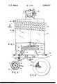
- FIG. 1illustrates a glow discharge deposition system constructed in accordance with the principles of the present invention.
- FIG. 2is a section view taken along line 2--2 of FIG. 1.
- FIG. 3is a bottom view of the gas dispersion head 34 of FIG. 1.
- FIG. 1illustrates a glow discharge-flow system for producing dense and adhering coatings in accordance with the present invention wherein a reaction chamber 10 is positioned atop a base plate 12 and is sealed thereto by means of an O-ring gasket 14.
- Chamber 10has a generally cylindrical shape and is formed of a nonmetallic material, preferably quartz.
- a multiturn coil forming inductor 16is wound about the upper portion of chamber 10 and has its ends coupled to a radio frequency power source.
- the RF power sourcewould typically have a frequency of 13 megacycles and a power output of 300 watts.
- RF energyis coupled to the gas through the wall of the chamber 10 to form a highly luminous glow discharge zone in the chamber 10 within the zone enclosed by inductor 16.
- a circular aluminum block or plate 18Downstream of RF coil 16, below the gas dispersing device 34, there is a circular aluminum block or plate 18 having a thermostatically controlled heater element 20 positioned therebelow and supported on base plate 12 by legs 22.
- Aluminum block 18is slightly recessed to accommodate a semiconductor substrate 24 which is typically a circular wafer having a diameter of a few centimeters.
- Leads 26 which couple power to the thermostatically-controlled heating element 20are connected to insulated feed-through terminals 28 in the base plate 12, which in turn have an external power source connected thereto.
- Base plate 12has a centrally-located exhaust port 30 which is connected to a vacuum pump.
- a gas containing siliconis admitted to chamber 10 via inlet tube 32.
- this gasconsists of silane which has been diluted to a concentration of less than 5% in an inert gas.
- Tube 32extends axially through chamber 10 and is coupled to a gas dispersion head 34. Tube 32 may, alternatively, extend to any point on the chamber's walls, below RF coil 16, to effect a seal and inlet of diluted silane from an external source.
- Gas dispersion head 34whose bottom view is shown in FIG. 3, is circular in shape and is positioned immediately above substrate 24. A plurality of holes or jets 36 in gas dispersion head 34 uniformly distribute gas over the top surface of substrate 24 and their distance from the substrate to be coated is critical and is given in the tables below.
- a gas containing nitrogenis admitted to reaction chamber 10 via inlet tube 40 which is connected to a gas dispersion device 42 located near the top of the chamber.
- Gas dispersion device 42which is also shown in the sectional view 2--2 of FIG. 2, has a plurality of holes or jets 44 adapted to disperse gas uniformly through chamber 10.
- the gas admitted to inlet tube 40is pure nitrogen or argon, for the deposition of silicon nitride or silicon, respectively.
- a substrate 24is inserted within the chamber 10 and the system is pumped down by a vacuum pump to a pressure of a few microns Hg.
- Heating element 20is activated to heat the substrate to a temperature approximating 300° C.
- Nitrogen gasis admitted to the chamber via input tube 40, and diluted silane gas is admitted to the chamber via input tube 32.
- the RF power sourceis activated so as to create a glow discharge zone within the chamber in the vicinity of inductor 16.
- the nitrogen gasis activated as it flows through the discharge zone defined by coil 16 to form active species thereof.
- the diluted silane gasis dispersed immediately above the substrate and a reaction occurs with the activated nitrogen gas to provide a uniform coating of silicon nitride of improved quality on the surface of substrate 24.
Landscapes
- Chemical & Material Sciences (AREA)
- Engineering & Computer Science (AREA)
- Physics & Mathematics (AREA)
- Plasma & Fusion (AREA)
- General Chemical & Material Sciences (AREA)
- Chemical Kinetics & Catalysis (AREA)
- Materials Engineering (AREA)
- Mechanical Engineering (AREA)
- Metallurgy (AREA)
- Organic Chemistry (AREA)
- Chemical Vapour Deposition (AREA)
- Formation Of Insulating Films (AREA)
Abstract
Description
Si.sup.+ + SiH.sub.4 -- Si.sub.2 H.sub.2.sup.+ + H.sub.2
siH.sup.+ SiH.sub.4 -- Si.sub.2 H.sub.3.sup.+ + H.sub.2
siH.sub.3.sup.+ + SiH.sub.4 + Si.sub.2 H.sub.3.sup.+ + 2H
TABLE I __________________________________________________________________________Formation of Silicon Nitride by Glow Discharge Reactants: Pure nitrogen (99.999%) and binary mixture of silane (1.5%) in argon by volume. System: 150 mm. O.D. quartz reaction chamber connected to 330 liters/min. mechanical vacuum pump equipped with a charged foreline trap. Gaseous N-Si (wt. %).sup.(d) Reactant N.sub.2 Total RF Substrate Deposition Index.sup.(c) Ratio Ratio Pressure Pressure Power Temp. D.sup.(a) Rate Etch.sup.(b) of Re- in Deposited (N:Si) (μHg) (μHg) (W) (° C) (inch) (A/min) Rate fraction Film __________________________________________________________________________64:1 525 1075 100 320 15/16 120 10A/min -- -- 64:1 670 1370 100 320 15/16 185 22A/min 2.13 -- 76:1 800 1500 100 320 15/16 200 1/4A/sec 1.93 -- 76:1 800 1500 100 320 1-1/16 145 3A/sec -- -- 76:1 800 1500 125 285 15/16 175 4A/sec 1.95 -- 76:1 1600 3000 100 280 1 220 1.2A/sec 2.09 -- 76:1 1600 3000 125 320 1-1/32 250 1.2A/sec 2.07 -- 81:1 670 1220 100 320 15/16 145 0.9A/min -- -- 97:1 800 1350 100 320 15/16 150 2A/min 1.87 -- 76:1 1600 3000 150 280 3/4 360 1.5A/sec -- -- 76:1 1600 3000 125 280 1/2 600 0.5A/sec -- -- 76:1 1600 3000 140 280 3/8 650 0.5A/sec -- -- 97:1 1600 2700 130 280 3/8 550 -- -- -- __________________________________________________________________________131:1 2175 3275 140 280 3/8 500 -- -- -- 131:1 2750 4150 140 280 3/8 500 -- -- -- 131:1 2200 3300 175 300 3/4 625 0.35A/sec -- -- 131:1 2200 3300 150 300 3/4 550 0.3A/sec -- -- 170:1 2200 3000 150 300 3/4 475 0.45A/sec -- -- 190:1 2450 3300 150 300 3/4 465 0.6A/sec -- -- 300:1 2450 3000 150 300 3/4 <400 >1A/sec -- -- 131:1 2200 3300 150 300 3/4 600 0.3A/sec -- 23:77 131:1 2200 3300 200 300 3/4 610 0.4A/sec -- 25:75 131:1 2200 3300 250 300 3/4 625 0.45A/sec -- 28:72 170:1 2200 3000 200 300 3/4 500 0.5A/sec -- 25:75 170:1 2800 3900 250 300 3/4 550 0.83A/sec -- -- 190:1 2450 3300 200 300 3/4 500 0.6A/sec -- 32:68 __________________________________________________________________________
TABLE II __________________________________________________________________________Formation of Silicon Nitride Films by Glow Discharge Reactants: Pure nitrogen (99.999%) and binary mixture of silane (3%) in argon by volume. System: 150 mm. O.D. quartz reaction chamber connected to 330 liters/min. mechanical vacuum pump equipped with a charged foreline trap. Gaseous N-Si (wt. %) .sup.(d) Reactant N.sub.2 Total RF Substrate Deposition Index.sup.(c) Ratio Ratio Pressure Pressure Power Temp. D.sup.(a) Rate Etch.sup.(b) of Re- in Deposited (N:Si) (μHg) (μHg) (W) (° C) (inch) (A/min) Rate fraction Film __________________________________________________________________________150:1 2475 3025 250 300 3/4 425 -- -- -- 170:1 2875 3355 250 300 3/4 400 -- -- -- 190:1 3135 3685 250 300 3/4 450 -- -- -- __________________________________________________________________________
TABLE III __________________________________________________________________________Reactants: Pure nitrogen (99.999%) and binary mixture of silane (1.5%) in helium by volume. System: 150 mm. O.D. quartz reaction chamber connected to 330 liters/min. mechanical vacuum pump equipped with a charged foreline trap. Gaseous N-Si (wt. %) .sup.(d) Reactant N.sub.2 Total RF Substrate Deposition Index.sup.(c) Ratio Ratio Pressure Pressure Power Temp. D.sup.(a) Rate Etch.sup.(b) of Re- in Deposited (N:Si) (μHg) (μHg) (W) (° C) (inch) (A/min) Rate fraction Film __________________________________________________________________________ 90:1 700 1220 150 300 1 120 10 A/min -- -- 100:1 800 1333 150 300 1 150 11A/min -- -- __________________________________________________________________________
TABLE IV __________________________________________________________________________Formation of Silicon Films by Glow Discharge Reactants: Pure argon (99.99%) and binary mixture of silane (1.5%) in argon by volume. System: 150 mm. O.D. quartz reaction chamber connected to 330 liters/min. mechanical vacuum pump equipped with a charged foreline trap. Gaseous N-Si (wt. %) .sup.(d) Reactant N.sub.2 Total RF Substrate Deposition Index.sup.(c) Ratio Ratio Pressure Pressure Power Temp. D.sup.(a) Rate Etch.sup.(b) of Re- in Deposited (N:Si) (μHg) (μHg) (W) (° C) (inch) (A/min) Rate fraction Film __________________________________________________________________________76:1 1600 3000 140 280 1/4 700 -- -- -- 76:1 800 1500 100 280 1/4 360 -- -- -- 76:1 1600 3000 140 280 1/8 750 -- -- -- __________________________________________________________________________ Legend:- .sup.(a) Critical distance betweenmultiple jets 36 ingas dispersing device 34 and surface ofsubstrate 24 to be coated. .sup.(b) For the assessment of film density: etch rates designated in A/min refer to buffered HF etchant (45cc. HF (48%):200gr. NH.sub.4 F:300cc. H.sub.2 O); etch rates designated in A/sec refer to HF(48%) etchant. Etchants temperature: 25° C. .sup.(c) Measurements refer to ellipsometry at 5461 A. .sup.(d) Weight % ratios inferred from Auger Electron Spectroscopy determinations.
Claims (4)
Priority Applications (4)
| Application Number | Priority Date | Filing Date | Title |
|---|---|---|---|
| US05/641,441US4066037A (en) | 1975-12-17 | 1975-12-17 | Apparatus for depositing dielectric films using a glow discharge |
| GB50471/76AGB1533497A (en) | 1975-12-17 | 1976-12-03 | Apparatus and method for depositing dielectric films using a glow discharge |
| JP51148800AJPS5275983A (en) | 1975-12-17 | 1976-12-13 | Device for applying dielectric layer employing glow discharge |
| DE19762656821DE2656821A1 (en) | 1975-12-17 | 1976-12-15 | DEVICE AND METHOD FOR APPLYING A FILM ON A SUBSTRATE |
Applications Claiming Priority (1)
| Application Number | Priority Date | Filing Date | Title |
|---|---|---|---|
| US05/641,441US4066037A (en) | 1975-12-17 | 1975-12-17 | Apparatus for depositing dielectric films using a glow discharge |
Publications (1)
| Publication Number | Publication Date |
|---|---|
| US4066037Atrue US4066037A (en) | 1978-01-03 |
Family
ID=24572394
Family Applications (1)
| Application Number | Title | Priority Date | Filing Date |
|---|---|---|---|
| US05/641,441Expired - LifetimeUS4066037A (en) | 1975-12-17 | 1975-12-17 | Apparatus for depositing dielectric films using a glow discharge |
Country Status (4)
| Country | Link |
|---|---|
| US (1) | US4066037A (en) |
| JP (1) | JPS5275983A (en) |
| DE (1) | DE2656821A1 (en) |
| GB (1) | GB1533497A (en) |
Cited By (19)
| Publication number | Priority date | Publication date | Assignee | Title |
|---|---|---|---|---|
| US4223048A (en)* | 1978-08-07 | 1980-09-16 | Pacific Western Systems | Plasma enhanced chemical vapor processing of semiconductive wafers |
| WO1981000862A1 (en)* | 1979-09-20 | 1981-04-02 | Western Electric Co | Methods and apparatus for generating plasmas |
| US4262631A (en)* | 1979-10-01 | 1981-04-21 | Kubacki Ronald M | Thin film deposition apparatus using an RF glow discharge |
| US4264393A (en)* | 1977-10-31 | 1981-04-28 | Motorola, Inc. | Reactor apparatus for plasma etching or deposition |
| US4289797A (en)* | 1979-10-11 | 1981-09-15 | Western Electric Co., Incorporated | Method of depositing uniform films of Six Ny or Six Oy in a plasma reactor |
| US4353777A (en)* | 1981-04-20 | 1982-10-12 | Lfe Corporation | Selective plasma polysilicon etching |
| US4362766A (en)* | 1978-08-23 | 1982-12-07 | Siemens Aktiengesellschaft | Method for preparing a protective amorphous silicon passivating film on a semiconductor device |
| US4421592A (en)* | 1981-05-22 | 1983-12-20 | United Technologies Corporation | Plasma enhanced deposition of semiconductors |
| US4454835A (en)* | 1982-09-13 | 1984-06-19 | The United States Of America As Represented By The Secretary Of The Navy | Internal photolysis reactor |
| US4599069A (en)* | 1984-02-27 | 1986-07-08 | Anelva Corporation | Substrate holder for molecular beam epitaxy apparatus |
| US4609424A (en)* | 1981-05-22 | 1986-09-02 | United Technologies Corporation | Plasma enhanced deposition of semiconductors |
| US4651673A (en)* | 1982-09-02 | 1987-03-24 | At&T Technologies, Inc. | CVD apparatus |
| US4980307A (en)* | 1978-06-14 | 1990-12-25 | Fujitsu Limited | Process for producing a semiconductor device having a silicon oxynitride insulative film |
| US4997677A (en)* | 1987-08-31 | 1991-03-05 | Massachusetts Institute Of Technology | Vapor phase reactor for making multilayer structures |
| US5288527A (en)* | 1990-09-03 | 1994-02-22 | Saint Gobain Vitrage International C/O Saint Gobain Recherche | Silicon nitride thin films with improved properties |
| US5824158A (en)* | 1993-06-30 | 1998-10-20 | Kabushiki Kaisha Kobe Seiko Sho | Chemical vapor deposition using inductively coupled plasma and system therefor |
| EP0871199A3 (en)* | 1988-12-28 | 1998-11-04 | AT&T Corp. | Processes depending on plasma generation |
| US6245648B1 (en) | 1977-12-05 | 2001-06-12 | Plasma Physics Corporation | Method of forming semiconducting materials and barriers |
| WO2008014915A3 (en)* | 2006-07-31 | 2008-05-08 | Fraunhofer Ges Forschung | Method for the plasma treatment of a surface |
Families Citing this family (7)
| Publication number | Priority date | Publication date | Assignee | Title |
|---|---|---|---|---|
| FR2411897A2 (en)* | 1977-12-13 | 1979-07-13 | Alsthom Atlantique | RF sputtering of thin semiconductor films - using polarisation impedance and gas pressure gradient to give high deposition rate |
| JPS54160568A (en)* | 1978-06-09 | 1979-12-19 | Anelva Corp | Thin film forming equipment for discharge chemical reaction |
| JPS5595334A (en)* | 1979-01-10 | 1980-07-19 | Nec Corp | Preparation of semiconductor device |
| FR2456787A1 (en)* | 1979-05-18 | 1980-12-12 | Thomson Csf | MICROWAVE DEVICE FOR DEPOSITING THIN FILMS ON SOLIDS |
| US4517223A (en)* | 1982-09-24 | 1985-05-14 | Sovonics Solar Systems | Method of making amorphous semiconductor alloys and devices using microwave energy |
| US4455351A (en)* | 1983-06-13 | 1984-06-19 | At&T Bell Laboratories | Preparation of photodiodes |
| GB8620273D0 (en)* | 1986-08-20 | 1986-10-01 | Gen Electric Co Plc | Deposition of thin films |
Citations (9)
| Publication number | Priority date | Publication date | Assignee | Title |
|---|---|---|---|---|
| GB730669A (en)* | 1951-12-28 | 1955-05-25 | Erie Resistor Corp | Gas plating apparatus |
| US2884894A (en)* | 1956-11-02 | 1959-05-05 | Metallgesellschaft Ag | Apparatus for producing hard coatings on workpieces |
| GB1134352A (en)* | 1966-05-02 | 1968-11-20 | Siemens Ag | Improvements in or relating to the production of layers of a solid nitride of a semiconductor element on semiconductor crystals |
| US3424661A (en)* | 1966-09-01 | 1969-01-28 | Bell Telephone Labor Inc | Method of conducting chemical reactions in a glow discharge |
| US3460816A (en)* | 1962-01-02 | 1969-08-12 | Gen Electric | Fluxless aluminum brazing furnace |
| US3655438A (en)* | 1969-10-20 | 1972-04-11 | Int Standard Electric Corp | Method of forming silicon oxide coatings in an electric discharge |
| US3757733A (en)* | 1971-10-27 | 1973-09-11 | Texas Instruments Inc | Radial flow reactor |
| US3847652A (en)* | 1972-12-08 | 1974-11-12 | Nasa | Method of preparing water purification membranes |
| US3880112A (en)* | 1971-10-20 | 1975-04-29 | Commissariat Energie Atomique | Device for the preparation of thin films |
- 1975
- 1975-12-17USUS05/641,441patent/US4066037A/ennot_activeExpired - Lifetime
- 1976
- 1976-12-03GBGB50471/76Apatent/GB1533497A/ennot_activeExpired
- 1976-12-13JPJP51148800Apatent/JPS5275983A/enactiveGranted
- 1976-12-15DEDE19762656821patent/DE2656821A1/ennot_activeWithdrawn
Patent Citations (9)
| Publication number | Priority date | Publication date | Assignee | Title |
|---|---|---|---|---|
| GB730669A (en)* | 1951-12-28 | 1955-05-25 | Erie Resistor Corp | Gas plating apparatus |
| US2884894A (en)* | 1956-11-02 | 1959-05-05 | Metallgesellschaft Ag | Apparatus for producing hard coatings on workpieces |
| US3460816A (en)* | 1962-01-02 | 1969-08-12 | Gen Electric | Fluxless aluminum brazing furnace |
| GB1134352A (en)* | 1966-05-02 | 1968-11-20 | Siemens Ag | Improvements in or relating to the production of layers of a solid nitride of a semiconductor element on semiconductor crystals |
| US3424661A (en)* | 1966-09-01 | 1969-01-28 | Bell Telephone Labor Inc | Method of conducting chemical reactions in a glow discharge |
| US3655438A (en)* | 1969-10-20 | 1972-04-11 | Int Standard Electric Corp | Method of forming silicon oxide coatings in an electric discharge |
| US3880112A (en)* | 1971-10-20 | 1975-04-29 | Commissariat Energie Atomique | Device for the preparation of thin films |
| US3757733A (en)* | 1971-10-27 | 1973-09-11 | Texas Instruments Inc | Radial flow reactor |
| US3847652A (en)* | 1972-12-08 | 1974-11-12 | Nasa | Method of preparing water purification membranes |
Non-Patent Citations (1)
| Title |
|---|
| Western Electric Company, Inc., Technical Digest No. 11, July 1968, pp. 5, 6, Apparatus for the Deposition of Silicon Nitride, R. A. Whitner.* |
Cited By (21)
| Publication number | Priority date | Publication date | Assignee | Title |
|---|---|---|---|---|
| US4264393A (en)* | 1977-10-31 | 1981-04-28 | Motorola, Inc. | Reactor apparatus for plasma etching or deposition |
| US6245648B1 (en) | 1977-12-05 | 2001-06-12 | Plasma Physics Corporation | Method of forming semiconducting materials and barriers |
| US4980307A (en)* | 1978-06-14 | 1990-12-25 | Fujitsu Limited | Process for producing a semiconductor device having a silicon oxynitride insulative film |
| US4223048A (en)* | 1978-08-07 | 1980-09-16 | Pacific Western Systems | Plasma enhanced chemical vapor processing of semiconductive wafers |
| US4362766A (en)* | 1978-08-23 | 1982-12-07 | Siemens Aktiengesellschaft | Method for preparing a protective amorphous silicon passivating film on a semiconductor device |
| WO1981000862A1 (en)* | 1979-09-20 | 1981-04-02 | Western Electric Co | Methods and apparatus for generating plasmas |
| US4282267A (en)* | 1979-09-20 | 1981-08-04 | Western Electric Co., Inc. | Methods and apparatus for generating plasmas |
| US4262631A (en)* | 1979-10-01 | 1981-04-21 | Kubacki Ronald M | Thin film deposition apparatus using an RF glow discharge |
| US4289797A (en)* | 1979-10-11 | 1981-09-15 | Western Electric Co., Incorporated | Method of depositing uniform films of Six Ny or Six Oy in a plasma reactor |
| US4353777A (en)* | 1981-04-20 | 1982-10-12 | Lfe Corporation | Selective plasma polysilicon etching |
| US4609424A (en)* | 1981-05-22 | 1986-09-02 | United Technologies Corporation | Plasma enhanced deposition of semiconductors |
| US4421592A (en)* | 1981-05-22 | 1983-12-20 | United Technologies Corporation | Plasma enhanced deposition of semiconductors |
| US4651673A (en)* | 1982-09-02 | 1987-03-24 | At&T Technologies, Inc. | CVD apparatus |
| US4454835A (en)* | 1982-09-13 | 1984-06-19 | The United States Of America As Represented By The Secretary Of The Navy | Internal photolysis reactor |
| US4599069A (en)* | 1984-02-27 | 1986-07-08 | Anelva Corporation | Substrate holder for molecular beam epitaxy apparatus |
| US4997677A (en)* | 1987-08-31 | 1991-03-05 | Massachusetts Institute Of Technology | Vapor phase reactor for making multilayer structures |
| EP0871199A3 (en)* | 1988-12-28 | 1998-11-04 | AT&T Corp. | Processes depending on plasma generation |
| US5288527A (en)* | 1990-09-03 | 1994-02-22 | Saint Gobain Vitrage International C/O Saint Gobain Recherche | Silicon nitride thin films with improved properties |
| US5824158A (en)* | 1993-06-30 | 1998-10-20 | Kabushiki Kaisha Kobe Seiko Sho | Chemical vapor deposition using inductively coupled plasma and system therefor |
| WO2008014915A3 (en)* | 2006-07-31 | 2008-05-08 | Fraunhofer Ges Forschung | Method for the plasma treatment of a surface |
| US20100032285A1 (en)* | 2006-07-31 | 2010-02-11 | Fraunhofer-Gesellschaft Zur Forderung Der Angewandten Forschung E.V. | Method of plasma treatment of a surface |
Also Published As
| Publication number | Publication date |
|---|---|
| JPS5275983A (en) | 1977-06-25 |
| JPS5433956B2 (en) | 1979-10-24 |
| GB1533497A (en) | 1978-11-29 |
| DE2656821A1 (en) | 1977-06-30 |
Similar Documents
| Publication | Publication Date | Title |
|---|---|---|
| US4066037A (en) | Apparatus for depositing dielectric films using a glow discharge | |
| JP2596214B2 (en) | Method of forming high-purity thin film | |
| KR102009923B1 (en) | Processing method of silicon nitride film and forming method of silicon nitride film | |
| KR101295604B1 (en) | A method and apparatus for forming a high quality low temperature silicon nitride layer | |
| KR970002437B1 (en) | Fabricating method of semiconductor device | |
| EP0584252B1 (en) | A PROCESS FOR DEPOSITING A SIOx FILM HAVING REDUCED INTRINSIC STRESS AND/OR REDUCED HYDROGEN CONTENT | |
| JP3688726B2 (en) | Manufacturing method of semiconductor device | |
| US4262631A (en) | Thin film deposition apparatus using an RF glow discharge | |
| US5385763A (en) | Method for forming a film on a substrate by activating a reactive gas | |
| US4683838A (en) | Plasma treatment system | |
| US20070128880A1 (en) | Process and apparatus for forming oxide film, and electronic device material | |
| US4992299A (en) | Deposition of silicon nitride films from azidosilane sources | |
| JPS6243335B2 (en) | ||
| JPH02236282A (en) | Production of silicon-containing coating,using organosilicic compound and nitrogen trifluoride | |
| US20120153442A1 (en) | Silicon nitride film and process for production thereof, computer-readable storage medium, and plasma cvd device | |
| US5763021A (en) | Method of forming a dielectric film | |
| US6159559A (en) | Low temperature, high quality silicon dioxide thin films deposited using tetramethylsilane (TMS) | |
| US20050227500A1 (en) | Method for producing material of electronic device | |
| EP1030352A2 (en) | Method and apparatus for forming materials layers from atomic gases | |
| Alexandrov et al. | Formation of silicon nitride films by remote plasma‐enhanced chemical vapour deposition | |
| KR20110055702A (en) | Silicon nitride film and formation method thereof, computer readable storage medium, and plasma CD device | |
| JPH06168937A (en) | Manufacture of silicon oxide film | |
| US5510088A (en) | Low temperature plasma film deposition using dielectric chamber as source material | |
| GB2132637A (en) | Process for depositing dielectric films in a plasma glow discharge | |
| KR20220051192A (en) | PEALD Titanium Nitride Using Direct Microwave Plasma |
Legal Events
| Date | Code | Title | Description |
|---|---|---|---|
| AS | Assignment | Owner name:MARINE MIDLAND BANK, N.A., ONE MIDLAND CENTER, BUF Free format text:SECURITY INTEREST;ASSIGNOR:LFE CORPORATION, A CORP. OF DE.;REEL/FRAME:004526/0096 Effective date:19860214 | |
| AS | Assignment | Owner name:MARINE MIDLAND BANK, N.A., ONE MARINE MIDLAND CENT Free format text:SECURITY INTEREST;ASSIGNOR:LFE CORPORATION, A CORP. OF DE.;REEL/FRAME:004804/0379 Effective date:19870416 Owner name:MARINE MIDLAND BANK, N.A.,NEW YORK Free format text:SECURITY INTEREST;ASSIGNOR:LFE CORPORATION, A CORP. OF DE.;REEL/FRAME:004804/0379 Effective date:19870416 | |
| AS | Assignment | Owner name:MARK IV INDUSTRIES, INC. Free format text:ASSIGNMENT OF ASSIGNORS INTEREST.;ASSIGNOR:MARK IV VENTURES INC.;REEL/FRAME:005020/0082 Effective date:19871231 Owner name:AUDUBON ENTERPRISES INC. Free format text:ASSIGNS TO EACH ASSIGNEE THE AMOUNT SPECIFIED BY THEIR RESPECTIVE NAMES.;ASSIGNOR:CONRAC CORPORATION;REEL/FRAME:005020/0035 Effective date:19871231 Owner name:MARK IV INDUSTRIES, INC. Free format text:ASSIGNMENT OF ASSIGNORS INTEREST.;ASSIGNOR:PARKWAY ENTERPRISES INC.;REEL/FRAME:005020/0046 Effective date:19871231 Owner name:AUDUBON VENTURES INC. Free format text:ASSIGNS TO EACH ASSIGNEE THE AMOUNT SPECIFIED BY THEIR RESPECTIVE NAMES.;ASSIGNOR:CONRAC CORPORATION;REEL/FRAME:005020/0035 Effective date:19871231 Owner name:AUDUBON INDUSTRIES INC. Free format text:ASSIGNS TO EACH ASSIGNEE THE AMOUNT SPECIFIED BY THEIR RESPECTIVE NAMES.;ASSIGNOR:CONRAC CORPORATION;REEL/FRAME:005020/0035 Effective date:19871231 Owner name:MARK IV INDUSTRIES, INC. Free format text:ASSIGNMENT OF ASSIGNORS INTEREST.;ASSIGNOR:PARKWAY INDUSTRIES INC.;REEL/FRAME:005020/0064 Effective date:19871231 Owner name:MARK IV INDUSTRIES, INC. Free format text:ASSIGNMENT OF ASSIGNORS INTEREST.;ASSIGNOR:AUDUBON INDUSTRIES, INC.;REEL/FRAME:005020/0100 Effective date:19881231 Owner name:MARK IV INDUSTRIES, INC. Free format text:ASSIGNMENT OF ASSIGNORS INTEREST.;ASSIGNOR:PARKWAY VENTURES INC.;REEL/FRAME:005020/0109 Effective date:19871231 Owner name:MARK IV INDUSTRIES, INC., Free format text:ASSIGNMENT OF ASSIGNORS INTEREST.;ASSIGNOR:AUDUBORN HOLDINGS INC., A DE. CORP.;REEL/FRAME:005020/0118 Effective date:19871231 Owner name:AUDUBON HOLDINGS INC. Free format text:ASSIGNS TO EACH ASSIGNEE THE AMOUNT SPECIFIED BY THEIR RESPECTIVE NAMES.;ASSIGNOR:CONRAC CORPORATION;REEL/FRAME:005020/0035 Effective date:19871231 Owner name:MARK IV INDUSTRIES, INC. Free format text:ASSIGNMENT OF ASSIGNORS INTEREST.;ASSIGNOR:MARK IV HOLDINGS INC.;REEL/FRAME:005020/0073 Effective date:19871231 Owner name:PARKWAY HOLDINGS INC. Free format text:ASSIGNS TO EACH ASSIGNEE THE AMOUNT SPECIFIED BY THEIR RESPECTIVE NAMES.;ASSIGNOR:CONRAC CORPORATION;REEL/FRAME:005020/0035 Effective date:19871231 Owner name:MARK IV INDUSTRIES, INC. Free format text:ASSIGNMENT OF ASSIGNORS INTEREST.;ASSIGNOR:AUDUBON VENTURES INC.;REEL/FRAME:005020/0055 Effective date:19871231 Owner name:MARK IV VENTURES INC. Free format text:ASSIGNS TO EACH ASSIGNEE THE AMOUNT SPECIFIED BY THEIR RESPECTIVE NAMES.;ASSIGNOR:CONRAC CORPORATION;REEL/FRAME:005020/0035 Effective date:19871231 Owner name:PARKWAY VENTURES INC. Free format text:ASSIGNS TO EACH ASSIGNEE THE AMOUNT SPECIFIED BY THEIR RESPECTIVE NAMES.;ASSIGNOR:CONRAC CORPORATION;REEL/FRAME:005020/0035 Effective date:19871231 Owner name:MARK IV INDUSTRIES INC. Free format text:ASSIGNMENT OF ASSIGNORS INTEREST.;ASSIGNOR:AUDUBON ENTERPRISES INC.;REEL/FRAME:005020/0091 Effective date:19871231 Owner name:PARKWAY ENTERPRISES INC. Free format text:ASSIGNS TO EACH ASSIGNEE THE AMOUNT SPECIFIED BY THEIR RESPECTIVE NAMES.;ASSIGNOR:CONRAC CORPORATION;REEL/FRAME:005020/0035 Effective date:19871231 Owner name:MARK IV INDUSTRIES, INC. Free format text:ASSIGNMENT OF ASSIGNORS INTEREST.;ASSIGNOR:PARKWAY HOLDINGS INC.;REEL/FRAME:005044/0710 Effective date:19871231 Owner name:MARK IV HOLDINGS INC. Free format text:ASSIGNS TO EACH ASSIGNEE THE AMOUNT SPECIFIED BY THEIR RESPECTIVE NAMES.;ASSIGNOR:CONRAC CORPORATION;REEL/FRAME:005020/0035 Effective date:19871231 Owner name:CODE-A-PHONE CORPORATION Free format text:MERGER;ASSIGNOR:LFE CORPORATION, (MERGED INTO);REEL/FRAME:005020/0027 Effective date:19870930 Owner name:PARKWAY INDUSTRIES INC. Free format text:ASSIGNS TO EACH ASSIGNEE THE AMOUNT SPECIFIED BY THEIR RESPECTIVE NAMES.;ASSIGNOR:CONRAC CORPORATION;REEL/FRAME:005020/0035 Effective date:19871231 | |
| AS | Assignment | Owner name:LFE CORPORATION Free format text:RELEASED BY SECURED PARTY;ASSIGNOR:MARINE MIDLAND BANK, N.A.;REEL/FRAME:005041/0045 Effective date:19880223 | |
| STCF | Information on status: patent grant | Free format text:PATENTED FILE - (OLD CASE ADDED FOR FILE TRACKING PURPOSES) | |
| AS | Assignment | Owner name:CONRAC CORPORATION (80%) Free format text:ASSIGNS TO EACH ASSIGNEE THE PERCENTAGES OPPOSITE THEIR RESPECTIVE NAME;ASSIGNOR:CODE-A-PHONE CORPORATION, A CORP. DE;REEL/FRAME:005136/0610 Effective date:19871231 Owner name:MARK IV INDUSTRIES, INC., (20%) Free format text:ASSIGNS TO EACH ASSIGNEE THE PERCENTAGES OPPOSITE THEIR RESPECTIVE NAME;ASSIGNOR:CODE-A-PHONE CORPORATION, A CORP. DE;REEL/FRAME:005136/0610 Effective date:19871231 |