US4013889A - Electronic amplification - Google Patents
Electronic amplificationDownload PDFInfo
- Publication number
- US4013889A US4013889AUS05/584,854US58485475AUS4013889AUS 4013889 AUS4013889 AUS 4013889AUS 58485475 AUS58485475 AUS 58485475AUS 4013889 AUS4013889 AUS 4013889A
- Authority
- US
- United States
- Prior art keywords
- amplifier
- detector
- channel
- signal
- coupled
- Prior art date
- Legal status (The legal status is an assumption and is not a legal conclusion. Google has not performed a legal analysis and makes no representation as to the accuracy of the status listed.)
- Expired - Lifetime
Links
Images
Classifications
- H—ELECTRICITY
- H04—ELECTRIC COMMUNICATION TECHNIQUE
- H04N—PICTORIAL COMMUNICATION, e.g. TELEVISION
- H04N5/00—Details of television systems
- H04N5/30—Transforming light or analogous information into electric information
Definitions
- a multi-element array of detector elementsis used to scan an image of the field of view.
- the different detectorsscan different parts of the scene and, generally, each detector is provided with its own video amplifying channel and is coupled to its respective amplifier by means of a.c. coupling.
- a.c. couplingsince different detectors scan different parts of the scene, their output wave forms will in general be different and the a.c. coupling will progressively charge in each raster scan to result in different mean voltages.
- To produce an image of the scene with high fidelityit becomes necessary to make the a.c. coupling time constants long enough to prevent the differences in the voltages taken up by the different a.c.
- This inventionrelates to scanning arrangements which are suitable for but not necessarily restricted to surveillance systems. Herein it is described in relation to surveillance scanners. It has as its object the provision of scanning apparatus in which the detector video amplifier channels have improved characteristics.
- the radiation output of the reference sourcemay sometimes differ greatly from the radiation received from the field of view and under these circumstances large differences between the detector outputs when viewing the reference source and when viewing the scene may be unavoidable. In such circumstances unless the gains of the different detector amplifiers are precisely the same, the display output which is set equal when viewing the reference source will nevertheless differ when viewing a uniform area of the scene.
- scanning apparatushaving a multidetector array which traverses a field of view, the detectors of which are sensitive to variations in electromagnetic radiation and wherein each detector is a.c. coupled to an amplifier in a respective video channel and means which equalizes the gains of the amplifiers in the said channels one with another at the end of each scan.
- Said meansmay comprise a reference a.c. source, switch means for temporarily switching the a.c. source into the inputs of each detector amplifier at the end of each scan in lieu of the output of the respective detector, and, for each channel, respective controllable attenuator means controlling the gain of the detector amplifier and an integrating amplifier means which compares the output of the detector amplifier when the latter is coupled to the a.c. reference source with a further reference signal, integrates any resultant difference signal and applies the integrand signal as a drive for the said controllable attenuator means thereby resetting the gain of the channel so as to reduce the said difference signal to zero.
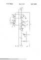
- the main amplifier 3has an inverting input 5, a non-inverting input 6 and an output 7. Output 7 is connected to a potential dividing network comprising series connected resistors r 1 and r 2 . The junction between resistors r 1 and r 2 is connected to the inverting input of the said amplifier.
- the non-inverting input 6 of the amplifier 3is connected to receive a signal from an attenuator circuit 8, the latter being in turn connected to receive from a switch circuit 9 either the video input from the pre-amplifier 2 or a 20 KHz reference signal from an input terminal 10.
- Switch circuit 9may comprise a standard gate driver integrated circuit such as that supplied by Siliconix Type No. DG188. Gate driver circuit 9 exhibits two stable conditions.
- a first conditionwhich corresponds to a first voltage level on gate input 11, results in the video signal from the detector being fed to the attenuator 8.
- the second conditionwhich corresponds to a second voltage level applied to gate 11 results in the 20 KHz reference signal being applied to the attenuator 8.
- the second voltage levelis provided in the form of a pulse at terminal 12 at the end of each scan.
- the attenuator 8comprises a two-stage setting device, there being a series connected resistor r 3 , r 4 and a shunt connected FET 13, 14 in each stage thereof.
- AGC circuit 4sets a d.c. voltage on each of the capacitors C 1 , C 2 which voltage is therefore always present on the respective gates of the FET's 13, 14.
- Each FETconstitutes variable resistance which shunts the input of the main amplifier.
- AGC circuit 4comprises a second amplifier 15 having a non-reversing input 16, a reversing input 17 and an output 18.
- the output 18is connected to the capacitors C 1 , C 2 via respective resistances r 5 , r 6 and to the gates of the said FET's 13, 14. It is also connected to the non-inverting input 16 of the second amplifier 15 via an integrating capacitor C 3 .
- the inverting input 17 of the amplifier 15is connected to a d.c. reference signal provided on terminal 19.
- the non-inverting input 16 of the second amplifier 15also receives a signal from the output of the main amplifier 3 via an a.c. coupling circuit 20, a switch 21 and a negative peak voltage detecting circuit 22 of conventional form.
- Switch 21constitutes a second gate driver similar to the first and may be such as that supplied by Siliconex Type DG181. This switch is normally open circuited during the normal scan period and is closed during the period that the 20 KHz reference signal is connected onto the attenuator 8, being connected to receive the control signal on terminal 12.
- a third switch 23is connected between the junction of the a.c. coupling circuit 20 and the main amplifier 3 output on the one hand and the output terminal 24 on the other. This switch is closed during the normal scan period and is open circuited during the period that the 20 KHz reference signal is connected onto the attenuator 8, being connected to receive the control signal on terminal 12.
- Switch 23constitutes a third gate driver and may be such as that supplied by Siliconex Type No. DG184.
- the circuitoperates in the following manner.
- the respective amplifier 3receives a video signal from its respective pre-amplifier via a presetting potentiometer 25, switch 9 and attenuator 8 and it supplies an output signal to terminal 24 via switch 23.
- switch 21is open circuited and switch 23 is closed.
- all three switches 9, 21 and 23are responsive to a pulse on terminal 12 such that the 20 KHz reference signal is now connected to the attenuator 8, switch 21 is closed thus coupling amplifier 15 to the rectified output of amplifier 3, and switch 23 is open circuited. Any difference between the d.c.
- the detectorsmay be chosen for sensitivity to any part of the electro-magnetic spectrum.
Landscapes
- Engineering & Computer Science (AREA)
- Multimedia (AREA)
- Signal Processing (AREA)
- Transforming Light Signals Into Electric Signals (AREA)
- Photometry And Measurement Of Optical Pulse Characteristics (AREA)
- Picture Signal Circuits (AREA)
- Measurement Of Radiation (AREA)
- Amplifiers (AREA)
- Closed-Circuit Television Systems (AREA)
Abstract
Description
Claims (7)
Applications Claiming Priority (2)
| Application Number | Priority Date | Filing Date | Title |
|---|---|---|---|
| UK26234/74 | 1974-06-13 | ||
| GB26234/74AGB1511234A (en) | 1975-05-23 | 1975-05-23 | Electronic amplification |
Publications (1)
| Publication Number | Publication Date |
|---|---|
| US4013889Atrue US4013889A (en) | 1977-03-22 |
Family
ID=10240446
Family Applications (1)
| Application Number | Title | Priority Date | Filing Date |
|---|---|---|---|
| US05/584,854Expired - LifetimeUS4013889A (en) | 1974-06-13 | 1975-06-09 | Electronic amplification |
Country Status (5)
| Country | Link |
|---|---|
| US (1) | US4013889A (en) |
| DE (1) | DE2526375C3 (en) |
| FR (1) | FR2275088A1 (en) |
| GB (1) | GB1511234A (en) |
| SE (1) | SE404120B (en) |
Cited By (2)
| Publication number | Priority date | Publication date | Assignee | Title |
|---|---|---|---|---|
| US4276474A (en)* | 1979-10-22 | 1981-06-30 | Hughes Aircraft Company | Infrared focal plane with automatic responsivity control using photodetector bias modulation |
| US4712010A (en)* | 1986-01-30 | 1987-12-08 | Hughes Aircraft Company | Radiator scanning with image enhancement and noise reduction |
Families Citing this family (1)
| Publication number | Priority date | Publication date | Assignee | Title |
|---|---|---|---|---|
| JPS57116477A (en)* | 1981-01-09 | 1982-07-20 | Fuji Xerox Co Ltd | Scanning type document reader |
Citations (2)
| Publication number | Priority date | Publication date | Assignee | Title |
|---|---|---|---|---|
| US3597617A (en)* | 1969-07-30 | 1971-08-03 | Barnes Eng Co | Infrared thermograph having an automatic brightness control |
| US3808435A (en)* | 1973-05-29 | 1974-04-30 | Texas Instruments Inc | Infra-red quantum differential detector system |
- 1975
- 1975-05-23GBGB26234/74Apatent/GB1511234A/ennot_activeExpired
- 1975-06-06SESE7506495Apatent/SE404120B/enunknown
- 1975-06-09USUS05/584,854patent/US4013889A/ennot_activeExpired - Lifetime
- 1975-06-11FRFR7518242Apatent/FR2275088A1/enactiveGranted
- 1975-06-12DEDE2526375Apatent/DE2526375C3/ennot_activeExpired
Patent Citations (2)
| Publication number | Priority date | Publication date | Assignee | Title |
|---|---|---|---|---|
| US3597617A (en)* | 1969-07-30 | 1971-08-03 | Barnes Eng Co | Infrared thermograph having an automatic brightness control |
| US3808435A (en)* | 1973-05-29 | 1974-04-30 | Texas Instruments Inc | Infra-red quantum differential detector system |
Cited By (2)
| Publication number | Priority date | Publication date | Assignee | Title |
|---|---|---|---|---|
| US4276474A (en)* | 1979-10-22 | 1981-06-30 | Hughes Aircraft Company | Infrared focal plane with automatic responsivity control using photodetector bias modulation |
| US4712010A (en)* | 1986-01-30 | 1987-12-08 | Hughes Aircraft Company | Radiator scanning with image enhancement and noise reduction |
Also Published As
| Publication number | Publication date |
|---|---|
| DE2526375B2 (en) | 1980-02-28 |
| FR2275088A1 (en) | 1976-01-09 |
| SE7506495L (en) | 1975-12-15 |
| DE2526375A1 (en) | 1976-01-22 |
| DE2526375C3 (en) | 1980-10-23 |
| FR2275088B1 (en) | 1979-10-19 |
| GB1511234A (en) | 1978-05-17 |
| SE404120B (en) | 1978-09-18 |
Similar Documents
| Publication | Publication Date | Title |
|---|---|---|
| US3147341A (en) | Automatic brightness-contrast control using photoresistive element to control brightness and agc voltages in response to ambinent light | |
| US3970777A (en) | Apparatus for adjusting video pedestal and peak white level | |
| US4013889A (en) | Electronic amplification | |
| DE3621162C2 (en) | ||
| EP0809396A2 (en) | Automatic beam current limit apparatus and methods of the same | |
| US4551755A (en) | Television bandwidth correcting system | |
| US3389221A (en) | Television brightness compensation system | |
| US4598322A (en) | Video level control for CCD camera | |
| US3578908A (en) | Automatic peak video control system | |
| US4318129A (en) | Automatic level and gain control system | |
| US2834877A (en) | Automatic gain control circuits | |
| US3445590A (en) | Coordinated sensitivity and amplification control system | |
| US4229767A (en) | Beam control circuit for diode-gun type camera tubes | |
| US4000366A (en) | Adaptive gray scale control circuit for television video signals | |
| US4069505A (en) | Automatic peaking control circuitry for a video processing system | |
| US4947242A (en) | White balance control with adjusting means responsive to image brightness change | |
| US4237490A (en) | Signal overload prevention circuit | |
| CA2084728A1 (en) | Signal processing apparatus | |
| DE2742937C3 (en) | Video output amplifiers, in particular for color television signals | |
| EP0327229B1 (en) | Signal processing circuit and method | |
| US3518371A (en) | Preset sensitivity and amplification control system | |
| US4546291A (en) | Focus circuit for multi-tube image pick-up apparatus | |
| GB1585063A (en) | Display systems | |
| US2260963A (en) | Selecting circuit | |
| EP0217443B1 (en) | Picture signal processing circuit |
Legal Events
| Date | Code | Title | Description |
|---|---|---|---|
| AS | Assignment | Owner name:BRITISH AEROSPACE PUBLIC LIMITED COMPANY Free format text:CHANGE OF NAME;ASSIGNOR:BRITISH AEROSPACE LIMITED;REEL/FRAME:004080/0820 Effective date:19820106 Owner name:BRITISH AEROSPACE PUBLIC LIMITED COMPANY, DISTRICT Free format text:CHANGE OF NAME;ASSIGNOR:BRITISH AEROSPACE LIMITED;REEL/FRAME:004080/0820 Effective date:19820106 | |
| AS | Assignment | Owner name:BRITISH AEROSPACE, BROOKLANDS RD., WEYBRIDGE SURRE Free format text:ASSIGNOR HEREBY ASSIGNS NUNC PRO TUNC AS OF NOV. 22, 1978, THE ENTIRE INTEREST TO SAID ASSIGNEE TO SAID ASSIGNEE IN SAID PATENTS AND PATENT APPLICATIONS;ASSIGNOR:HAWKER SIDDELEY DYNAMICS LIMITED;REEL/FRAME:003949/0771 Effective date:19811218 Owner name:BRITISH AEROSPACE, ENGLAND Free format text:ASSIGNOR HEREBY ASSIGNS NUNC PRO TUNC AS OF NOV. 22, 1978, THE ENTIRE INTEREST TO SAID ASSIGNEE TO SAID ASSIGNEE IN SAID PATENTS AND PATENT APPLICATIONS;ASSIGNOR:HAWKER SIDDELEY DYNAMICS LIMITED;REEL/FRAME:003949/0771 Effective date:19811218 |