US3993909A - Substrate holder for etching thin films - Google Patents
Substrate holder for etching thin filmsDownload PDFInfo
- Publication number
- US3993909A US3993909AUS05/644,069US64406975AUS3993909AUS 3993909 AUS3993909 AUS 3993909AUS 64406975 AUS64406975 AUS 64406975AUS 3993909 AUS3993909 AUS 3993909A
- Authority
- US
- United States
- Prior art keywords
- turntable
- support
- substrate
- ion beam
- rotation
- Prior art date
- Legal status (The legal status is an assumption and is not a legal conclusion. Google has not performed a legal analysis and makes no representation as to the accuracy of the status listed.)
- Expired - Lifetime
Links
Images
Classifications
- H—ELECTRICITY
- H01—ELECTRIC ELEMENTS
- H01L—SEMICONDUCTOR DEVICES NOT COVERED BY CLASS H10
- H01L21/00—Processes or apparatus adapted for the manufacture or treatment of semiconductor or solid state devices or of parts thereof
- H01L21/67—Apparatus specially adapted for handling semiconductor or electric solid state devices during manufacture or treatment thereof; Apparatus specially adapted for handling wafers during manufacture or treatment of semiconductor or electric solid state devices or components ; Apparatus not specifically provided for elsewhere
- H01L21/683—Apparatus specially adapted for handling semiconductor or electric solid state devices during manufacture or treatment thereof; Apparatus specially adapted for handling wafers during manufacture or treatment of semiconductor or electric solid state devices or components ; Apparatus not specifically provided for elsewhere for supporting or gripping
- H01L21/687—Apparatus specially adapted for handling semiconductor or electric solid state devices during manufacture or treatment thereof; Apparatus specially adapted for handling wafers during manufacture or treatment of semiconductor or electric solid state devices or components ; Apparatus not specifically provided for elsewhere for supporting or gripping using mechanical means, e.g. chucks, clamps or pinches
- H01L21/68714—Apparatus specially adapted for handling semiconductor or electric solid state devices during manufacture or treatment thereof; Apparatus specially adapted for handling wafers during manufacture or treatment of semiconductor or electric solid state devices or components ; Apparatus not specifically provided for elsewhere for supporting or gripping using mechanical means, e.g. chucks, clamps or pinches the wafers being placed on a susceptor, stage or support
- H01L21/68764—Apparatus specially adapted for handling semiconductor or electric solid state devices during manufacture or treatment thereof; Apparatus specially adapted for handling wafers during manufacture or treatment of semiconductor or electric solid state devices or components ; Apparatus not specifically provided for elsewhere for supporting or gripping using mechanical means, e.g. chucks, clamps or pinches the wafers being placed on a susceptor, stage or support characterised by a movable susceptor, stage or support, others than those only rotating on their own vertical axis, e.g. susceptors on a rotating caroussel
- H—ELECTRICITY
- H01—ELECTRIC ELEMENTS
- H01L—SEMICONDUCTOR DEVICES NOT COVERED BY CLASS H10
- H01L21/00—Processes or apparatus adapted for the manufacture or treatment of semiconductor or solid state devices or of parts thereof
- H01L21/67—Apparatus specially adapted for handling semiconductor or electric solid state devices during manufacture or treatment thereof; Apparatus specially adapted for handling wafers during manufacture or treatment of semiconductor or electric solid state devices or components ; Apparatus not specifically provided for elsewhere
- H01L21/67005—Apparatus not specifically provided for elsewhere
- H01L21/67011—Apparatus for manufacture or treatment
- H01L21/67017—Apparatus for fluid treatment
- H01L21/67063—Apparatus for fluid treatment for etching
- H01L21/67069—Apparatus for fluid treatment for etching for drying etching
- H—ELECTRICITY
- H01—ELECTRIC ELEMENTS
- H01L—SEMICONDUCTOR DEVICES NOT COVERED BY CLASS H10
- H01L21/00—Processes or apparatus adapted for the manufacture or treatment of semiconductor or solid state devices or of parts thereof
- H01L21/67—Apparatus specially adapted for handling semiconductor or electric solid state devices during manufacture or treatment thereof; Apparatus specially adapted for handling wafers during manufacture or treatment of semiconductor or electric solid state devices or components ; Apparatus not specifically provided for elsewhere
- H01L21/683—Apparatus specially adapted for handling semiconductor or electric solid state devices during manufacture or treatment thereof; Apparatus specially adapted for handling wafers during manufacture or treatment of semiconductor or electric solid state devices or components ; Apparatus not specifically provided for elsewhere for supporting or gripping
- H01L21/687—Apparatus specially adapted for handling semiconductor or electric solid state devices during manufacture or treatment thereof; Apparatus specially adapted for handling wafers during manufacture or treatment of semiconductor or electric solid state devices or components ; Apparatus not specifically provided for elsewhere for supporting or gripping using mechanical means, e.g. chucks, clamps or pinches
- H01L21/68714—Apparatus specially adapted for handling semiconductor or electric solid state devices during manufacture or treatment thereof; Apparatus specially adapted for handling wafers during manufacture or treatment of semiconductor or electric solid state devices or components ; Apparatus not specifically provided for elsewhere for supporting or gripping using mechanical means, e.g. chucks, clamps or pinches the wafers being placed on a susceptor, stage or support
- H01L21/68771—Apparatus specially adapted for handling semiconductor or electric solid state devices during manufacture or treatment thereof; Apparatus specially adapted for handling wafers during manufacture or treatment of semiconductor or electric solid state devices or components ; Apparatus not specifically provided for elsewhere for supporting or gripping using mechanical means, e.g. chucks, clamps or pinches the wafers being placed on a susceptor, stage or support characterised by supporting more than one semiconductor substrate
Definitions
- the inventionrelates to a substrate holder for etching thin films by means of an ion beam, which holder is provided with a driving device adapted to move a substrate placed on a turntable with respect to the ion beam.
- Ion etching of surface structures in layers locally covered by masks between two electrodesyield etched structures having edges lacking in steepness.
- etching by means of a beam of collimated ionsprovides steep edges and permits etching geometries of a few microns with structure depths of several microns (see E. G. Spencer and P. H. Schmidt, Journal of Vacuum Science Technology 8, page 52 (1971)).
- the conventional ion beam gunsemit ion beams of less than 2 mm in diameter, a film having transverse dimensions exceeding those of the beam are to be moved to enable their surfaces to be uniformly etched.
- Substrate holderscapable of translatory and rotary motions are known.
- the apparatusgenerally referred to as "Schuur's Pendulum" which is marketed by the firm of Balzers of Liechtenstein, however, does not produce plane surfaces, because the two motions are independent of one another.
- a substrate holder according to the inventionis characterized by a friction disk which is adapted to rotate in rolling contact with a face of the turntable or of a driving disk carrying the turntable and which is spaced from the shaft of the driving disk by a radial distance equal to the radial distance by which the point of impact of the ion beam on the substrate is spaced therefrom.
- the feed of the substrate and the time of action of the ion beamalways are in the same ratio. This means that the ion beam always acts on each area of the substrate in the same manner, irrespective of whether this area of the substrate is near the driving disk shaft or remote therefrom. This ensures uniform etching.
- the shaft of the driving diskis supported for rotation in a nut which is displaceable by means of a lead screw which extends at right angles to the shaft and is rotatable by means of the shaft via a drive, the nut being displaced in the direction of length of the lead screw.
- the rotating driving diskis displaced in a vertical direction at right angles to the shaft. This dispenses with the need for an additional drive.
- the known apparatusfurthermore lacks a capability of motion which is of importance for ion etching of structures with the aid of masks.
- This motionis a rotation of the substrate about a second axis parallel to the first mentioned axis.
- the turntablecarries supports for the substrates, each support being intermittently rotatable about its axis, which extends parallel to the driving shaft, by means of a sprocket wheel during rotation of the driving disk.
- the supports carrying the substratespreferably are evenly distributed on the turntable at equal distances from the turntable axis.
- a pawlmay be made to engage with the sprocket wheels of the supports.
- the angle of incidence of the ion beam with respect to the normal to the film to be etchedis different from zero.
- the ion beamis required to successively pass through all directions on the curved surface of a cone having a vertical angle equal to the angle of incidence in order to avoid "shadow action" of the edges of the film structure.
- the turntable together with the driving disk and at least part of the driving deviceis rotatable about an axis that coincides with the vertical passing through the center of the turntable.
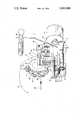
- a frame 1on which is mounted a motor 3 which drives a shaft 7 via a gearing 5.
- the shaft 7, which also is journalled in the frame 1,carries a bevel gearwheel 9 which meshes with a second bevel gearwheel 11 on a transmission shaft 13.
- the shaft 13drives a shaft 17 on which is mounted a friction disk 19.
- the shaft 17is journalled in a casing 21 which is pivotable through at least 90° about the axis 23 of the shaft 13.
- a ring 25 of the casing 21rests on a shoulder 27 of the frame 1.
- the casinghas a guide 29 in which a lead screw 31 is mounted for rotation.
- the lead screw 31carries a nut 33 in which a shaft 35 is journalled to which are secured, in spaced parallel relationship, a driving disk 37 and a turntable 39 for substrate supports.
- the friction disk 19runs on a face 41 of the driving disk 37.
- the friction disk 19rotates the disk 37 and hence the turntable 39 and the shaft 35.
- Rotation of the shaft 35causes a worm 43 to drive a wormwheel 45 which rotates the lead screw 31.
- the shaft 35 together with the disk 37 and the turntable 39are raised and lowered in the directions indicated by a double-headed arrow 46.
- the turntable 39carries supports 47 for substrates.
- the supports 47are evenly distributed on the turntable 39 at equal radial distances from the shaft 35.
- an ion beam 49is directed onto the substrates.
- the ion beam 49extends in the plane of the friction disk 19 so as to impinge on the substrates mounted on the supports 47.
- the supports 47due to the raising and lowering of the shaft 35 the material of the substrates is evenly removed.
- sprocket wheels 51are secured to the supports 47.
- the sprocket wheels 51may intermittently be rotated by means of a pawl 53 which may be caused at will to engage these wheels.
- the pawl 53may be moved into, or retracted from, the path of a sprocket wheel 51 at will by means of a control device 55.
- a double-headed arrow 57indicates a further capability of motion of the substrates.
- the casing 21can perform the aforementioned pivotal movement about the axis 23. This axis is in line with the vertical 59 passing through the centre of the turntable 39.
- the dwell time of the ion beam at each location of a substrateis equal, which means uniform etching.
- the casing 21is pivoted about the axis 23 through an angle such that the surface of the substrate contains the axis 23.
- the apparatusmay be extended in that, in addition to the coupled motions, the translation and rotation of the turntable and the substrate support may also be separately controlled so as to enable the substrates to be etched via motor pulses only.
- the inventionWhen combined with an ion beam source and a photolithographic masking technique the invention enables manufacture of plane surfaces having groove structures of high edge steepness (equal to or greater than 80°), high lateral resolution (more than 700 lines/mm) and large groove depth (more than 3 microns). In addition, in principle plane-parallel films are obtainable with a thickness tolerance of less than 0.1 micron.
Landscapes
- Engineering & Computer Science (AREA)
- Physics & Mathematics (AREA)
- Condensed Matter Physics & Semiconductors (AREA)
- General Physics & Mathematics (AREA)
- Manufacturing & Machinery (AREA)
- Computer Hardware Design (AREA)
- Microelectronics & Electronic Packaging (AREA)
- Power Engineering (AREA)
- ing And Chemical Polishing (AREA)
Abstract
Description
This is a continuation of application Ser. No. 450,742, filed Mar. 13, 1974 abandoned.
The invention relates to a substrate holder for etching thin films by means of an ion beam, which holder is provided with a driving device adapted to move a substrate placed on a turntable with respect to the ion beam.
Ion etching of surface structures in layers locally covered by masks between two electrodes (back-sputtering or sputter-etching) yield etched structures having edges lacking in steepness. By contrast, etching by means of a beam of collimated ions provides steep edges and permits etching geometries of a few microns with structure depths of several microns (see E. G. Spencer and P. H. Schmidt, Journal of Vacuum Science Technology 8, page 52 (1971)). Because the conventional ion beam guns emit ion beams of less than 2 mm in diameter, a film having transverse dimensions exceeding those of the beam are to be moved to enable their surfaces to be uniformly etched.
Substrate holders capable of translatory and rotary motions are known. The apparatus generally referred to as "Schuur's Pendulum" which is marketed by the firm of Balzers of Liechtenstein, however, does not produce plane surfaces, because the two motions are independent of one another.
In the "Reciprocating Specimen Holder" marketed by Commonwealth Scientific, Virginia, USA, the two motions are made dependent upon one another by a disk cam control system, although the drives are separate. However, this apparatus also does not enable the film thickness to be maintained within the tolerances of ± 0.1 micron required for some uses.
It is an object of the present invention to provide a substrate holder which enables the film thickness to be maintained within the narrow permissible tolerances.
For this purpose a substrate holder according to the invention is characterized by a friction disk which is adapted to rotate in rolling contact with a face of the turntable or of a driving disk carrying the turntable and which is spaced from the shaft of the driving disk by a radial distance equal to the radial distance by which the point of impact of the ion beam on the substrate is spaced therefrom.
When the ion beam always impinges on the substrate at the location at which the friction disk runs on the driving disk, the feed of the substrate and the time of action of the ion beam always are in the same ratio. This means that the ion beam always acts on each area of the substrate in the same manner, irrespective of whether this area of the substrate is near the driving disk shaft or remote therefrom. This ensures uniform etching.
In another embodiment of the invention the shaft of the driving disk is supported for rotation in a nut which is displaceable by means of a lead screw which extends at right angles to the shaft and is rotatable by means of the shaft via a drive, the nut being displaced in the direction of length of the lead screw. Thus the rotating driving disk is displaced in a vertical direction at right angles to the shaft. This dispenses with the need for an additional drive.
The known apparatus furthermore lacks a capability of motion which is of importance for ion etching of structures with the aid of masks. This motion is a rotation of the substrate about a second axis parallel to the first mentioned axis. Hence in a further embodiment of the invention the turntable carries supports for the substrates, each support being intermittently rotatable about its axis, which extends parallel to the driving shaft, by means of a sprocket wheel during rotation of the driving disk. The supports carrying the substrates preferably are evenly distributed on the turntable at equal distances from the turntable axis. Preferably a pawl may be made to engage with the sprocket wheels of the supports.
To achieve steep edges it further is important that the angle of incidence of the ion beam with respect to the normal to the film to be etched is different from zero. Thus the ion beam is required to successively pass through all directions on the curved surface of a cone having a vertical angle equal to the angle of incidence in order to avoid "shadow action" of the edges of the film structure. For this purpose in a further embodiment of the invention the turntable together with the driving disk and at least part of the driving device is rotatable about an axis that coincides with the vertical passing through the center of the turntable.
An embodiment of the invention will now be described, by way of example, with reference to the accompanying diagrammatic drawing.
Referring now to the single FIGURE of the drawing, there is shown a frame 1 on which is mounted amotor 3 which drives a shaft 7 via agearing 5. The shaft 7, which also is journalled in the frame 1, carries abevel gearwheel 9 which meshes with asecond bevel gearwheel 11 on a transmission shaft 13. Via agearing 15 the shaft 13 drives ashaft 17 on which is mounted afriction disk 19. Theshaft 17 is journalled in acasing 21 which is pivotable through at least 90° about theaxis 23 of the shaft 13. For this purpose a ring 25 of thecasing 21 rests on a shoulder 27 of the frame 1.
The casing has aguide 29 in which alead screw 31 is mounted for rotation. Thelead screw 31 carries anut 33 in which ashaft 35 is journalled to which are secured, in spaced parallel relationship, adriving disk 37 and aturntable 39 for substrate supports. Thefriction disk 19 runs on aface 41 of thedriving disk 37. Thus thefriction disk 19 rotates thedisk 37 and hence theturntable 39 and theshaft 35. Rotation of theshaft 35 causes aworm 43 to drive awormwheel 45 which rotates thelead screw 31. Thus theshaft 35 together with thedisk 37 and theturntable 39 are raised and lowered in the directions indicated by a double-headed arrow 46.
Theturntable 39 carriessupports 47 for substrates. Thesupports 47 are evenly distributed on theturntable 39 at equal radial distances from theshaft 35.
To remove material from the substrates anion beam 49 is directed onto the substrates. Theion beam 49 extends in the plane of thefriction disk 19 so as to impinge on the substrates mounted on thesupports 47. During the vertical reciprocating movements of thesupports 47 due to the raising and lowering of theshaft 35 the material of the substrates is evenly removed.
A further capability of motion is given in thatsprocket wheels 51 are secured to thesupports 47. When thedisk 37 and theturntable 39 rotate thesprocket wheels 51 may intermittently be rotated by means of apawl 53 which may be caused at will to engage these wheels. Thepawl 53 may be moved into, or retracted from, the path of asprocket wheel 51 at will by means of acontrol device 55.
A double-headed arrow 57 indicates a further capability of motion of the substrates. By means of a device, not shown, thecasing 21 can perform the aforementioned pivotal movement about theaxis 23. This axis is in line with the vertical 59 passing through the centre of theturntable 39.
In the substrate holder according to the invention the dwell time of the ion beam at each location of a substrate is equal, which means uniform etching. To find the best angle of incidence of the ion beam on the substrates thecasing 21 is pivoted about theaxis 23 through an angle such that the surface of the substrate contains theaxis 23.
The apparatus may be extended in that, in addition to the coupled motions, the translation and rotation of the turntable and the substrate support may also be separately controlled so as to enable the substrates to be etched via motor pulses only.
When combined with an ion beam source and a photolithographic masking technique the invention enables manufacture of plane surfaces having groove structures of high edge steepness (equal to or greater than 80°), high lateral resolution (more than 700 lines/mm) and large groove depth (more than 3 microns). In addition, in principle plane-parallel films are obtainable with a thickness tolerance of less than 0.1 micron.
Claims (3)
1. In a substrate holder of the type wherein a rotating turntable is adapted for carrying a plurality of substrates past an etching ion beam, the ion beam impacting the substrate surfaces at a gradually varying radius from the rotation axis of the turntable, the rotation speed of the turntable being proportional to the gradually varying radius, the improvement comprising:
a rotatable support for each substrate journalled in the turntable so that the surface of the substrate to be etched may be rotated within its own plane, the rotation axis of each support being parallel to the rotation axis of the turntable; and
means for rotating each support by a fixed amount during each rotation of the turntable.
2. The improvement of claim 1 wherein the rotation axis of each support is placed from the rotation axis of the turntable by the same distance.
3. The improvement of claim 2 further characterized by a sprocket wheel coaxially attached to each support for rotating said support, said means for rotating each support by a fixed amount during each rotation of the turntable comprising a pawl adapted for contact with successive sprocket wheels during rotation of the turntable so that each sprocket wheel and the support carried thereby rotates by a fixed amount when said sprocket wheel passes said pawl.
Priority Applications (1)
| Application Number | Priority Date | Filing Date | Title |
|---|---|---|---|
| US05/644,069US3993909A (en) | 1973-03-16 | 1975-12-24 | Substrate holder for etching thin films |
Applications Claiming Priority (4)
| Application Number | Priority Date | Filing Date | Title |
|---|---|---|---|
| DT2313096 | 1973-03-16 | ||
| DE19732313096DE2313096A1 (en) | 1973-03-16 | 1973-03-16 | SAMPLE HOLDER FOR ETCHING THIN LAYERS |
| US45074274A | 1974-03-13 | 1974-03-13 | |
| US05/644,069US3993909A (en) | 1973-03-16 | 1975-12-24 | Substrate holder for etching thin films |
Related Parent Applications (1)
| Application Number | Title | Priority Date | Filing Date |
|---|---|---|---|
| US45074274AContinuation | 1973-03-16 | 1974-03-13 |
Publications (1)
| Publication Number | Publication Date |
|---|---|
| US3993909Atrue US3993909A (en) | 1976-11-23 |
Family
ID=27185140
Family Applications (1)
| Application Number | Title | Priority Date | Filing Date |
|---|---|---|---|
| US05/644,069Expired - LifetimeUS3993909A (en) | 1973-03-16 | 1975-12-24 | Substrate holder for etching thin films |
Country Status (1)
| Country | Link |
|---|---|
| US (1) | US3993909A (en) |
Cited By (41)
| Publication number | Priority date | Publication date | Assignee | Title |
|---|---|---|---|---|
| EP0017143A1 (en)* | 1979-04-06 | 1980-10-15 | Hitachi, Ltd. | Microwave plasma etching apparatus |
| FR2529383A1 (en)* | 1982-06-24 | 1983-12-30 | Commissariat Energie Atomique | MECHANICAL SCANNING TARGET HOLDER USABLE IN PARTICULAR FOR THE IMPLANTATION OF IORIS |
| US4877962A (en)* | 1987-04-30 | 1989-10-31 | Mitsubishi Denki Kabushiki Kaisha | Ion implantation method |
| US4909695A (en)* | 1986-04-04 | 1990-03-20 | Materials Research Corporation | Method and apparatus for handling and processing wafer-like materials |
| EP0579380A1 (en)* | 1992-06-16 | 1994-01-19 | Hughes Aircraft Company | Apparatus and method for scanning a two-dimensional surface of one or more objects |
| EP0692815A3 (en)* | 1994-07-11 | 1996-03-20 | Applied Materials Inc | Method and device for etching films in layers on wide substrates |
| US5895549A (en)* | 1994-07-11 | 1999-04-20 | Applied Komatsu Technology, Inc. | Method and apparatus for etching film layers on large substrates |
| US5985742A (en)* | 1997-05-12 | 1999-11-16 | Silicon Genesis Corporation | Controlled cleavage process and device for patterned films |
| US6027988A (en)* | 1997-05-28 | 2000-02-22 | The Regents Of The University Of California | Method of separating films from bulk substrates by plasma immersion ion implantation |
| US6221740B1 (en) | 1999-08-10 | 2001-04-24 | Silicon Genesis Corporation | Substrate cleaving tool and method |
| US6263941B1 (en) | 1999-08-10 | 2001-07-24 | Silicon Genesis Corporation | Nozzle for cleaving substrates |
| US6284631B1 (en) | 1997-05-12 | 2001-09-04 | Silicon Genesis Corporation | Method and device for controlled cleaving process |
| US6291326B1 (en) | 1998-06-23 | 2001-09-18 | Silicon Genesis Corporation | Pre-semiconductor process implant and post-process film separation |
| US6291313B1 (en) | 1997-05-12 | 2001-09-18 | Silicon Genesis Corporation | Method and device for controlled cleaving process |
| US6500732B1 (en) | 1999-08-10 | 2002-12-31 | Silicon Genesis Corporation | Cleaving process to fabricate multilayered substrates using low implantation doses |
| US6548382B1 (en) | 1997-07-18 | 2003-04-15 | Silicon Genesis Corporation | Gettering technique for wafers made using a controlled cleaving process |
| US7056808B2 (en) | 1999-08-10 | 2006-06-06 | Silicon Genesis Corporation | Cleaving process to fabricate multilayered substrates using low implantation doses |
| USRE39484E1 (en) | 1991-09-18 | 2007-02-06 | Commissariat A L'energie Atomique | Process for the production of thin semiconductor material films |
| US20090130392A1 (en)* | 1996-05-15 | 2009-05-21 | Commissariat A L'energie Atomique (Cea) | Method of producing a thin layer of semiconductor material |
| US20090277314A1 (en)* | 2008-05-07 | 2009-11-12 | Silicon Genesis Corporation | Layer transfer of films utilizing controlled shear region |
| US7776717B2 (en) | 1997-05-12 | 2010-08-17 | Silicon Genesis Corporation | Controlled process and resulting device |
| US7811900B2 (en) | 2006-09-08 | 2010-10-12 | Silicon Genesis Corporation | Method and structure for fabricating solar cells using a thick layer transfer process |
| US7902038B2 (en) | 2001-04-13 | 2011-03-08 | Commissariat A L'energie Atomique | Detachable substrate with controlled mechanical strength and method of producing same |
| US7960248B2 (en) | 2007-12-17 | 2011-06-14 | Commissariat A L'energie Atomique | Method for transfer of a thin layer |
| US8048766B2 (en) | 2003-06-24 | 2011-11-01 | Commissariat A L'energie Atomique | Integrated circuit on high performance chip |
| US8142593B2 (en) | 2005-08-16 | 2012-03-27 | Commissariat A L'energie Atomique | Method of transferring a thin film onto a support |
| US8187377B2 (en) | 2002-10-04 | 2012-05-29 | Silicon Genesis Corporation | Non-contact etch annealing of strained layers |
| US8193069B2 (en) | 2003-07-21 | 2012-06-05 | Commissariat A L'energie Atomique | Stacked structure and production method thereof |
| US8252663B2 (en) | 2009-06-18 | 2012-08-28 | Commissariat A L'energie Atomique Et Aux Energies Alternatives | Method of transferring a thin layer onto a target substrate having a coefficient of thermal expansion different from that of the thin layer |
| US8293619B2 (en) | 2008-08-28 | 2012-10-23 | Silicon Genesis Corporation | Layer transfer of films utilizing controlled propagation |
| US8309431B2 (en) | 2003-10-28 | 2012-11-13 | Commissariat A L'energie Atomique | Method for self-supported transfer of a fine layer by pulsation after implantation or co-implantation |
| US8330126B2 (en) | 2008-08-25 | 2012-12-11 | Silicon Genesis Corporation | Race track configuration and method for wafering silicon solar substrates |
| US8329557B2 (en) | 2009-05-13 | 2012-12-11 | Silicon Genesis Corporation | Techniques for forming thin films by implantation with reduced channeling |
| US8389379B2 (en) | 2002-12-09 | 2013-03-05 | Commissariat A L'energie Atomique | Method for making a stressed structure designed to be dissociated |
| US8471223B2 (en) | 2011-02-09 | 2013-06-25 | Leica Mikrosysteme Gmbh | Apparatus and method for sample preparation |
| US8470712B2 (en) | 1997-12-30 | 2013-06-25 | Commissariat A L'energie Atomique | Process for the transfer of a thin film comprising an inclusion creation step |
| US8778775B2 (en) | 2006-12-19 | 2014-07-15 | Commissariat A L'energie Atomique | Method for preparing thin GaN layers by implantation and recycling of a starting substrate |
| CN104233305A (en)* | 2014-09-10 | 2014-12-24 | 中国电子科技集团公司第四十八研究所 | Ion beam etching workpiece table |
| US8993410B2 (en) | 2006-09-08 | 2015-03-31 | Silicon Genesis Corporation | Substrate cleaving under controlled stress conditions |
| CN104532204A (en)* | 2015-01-13 | 2015-04-22 | 中国科学院光电技术研究所 | A vertical coating fixture |
| US20230287561A1 (en)* | 2022-03-14 | 2023-09-14 | Applied Materials, Inc. | Variable Rotation Rate Batch Implanter |
Citations (8)
| Publication number | Priority date | Publication date | Assignee | Title |
|---|---|---|---|---|
| GB1104106A (en) | 1965-10-29 | 1968-02-21 | Mullard Ltd | Mass spectrographic analysis of solid bodies |
| US3388099A (en)* | 1965-05-14 | 1968-06-11 | Monsanto Co | Terpolyamides |
| US3496029A (en)* | 1966-10-12 | 1970-02-17 | Ion Physics Corp | Process of doping semiconductor with analyzing magnet |
| US3497689A (en)* | 1966-07-12 | 1970-02-24 | Siemens Ag | Corpuscular ray device having a shiftable specimen stage |
| US3629577A (en)* | 1968-09-23 | 1971-12-21 | Siemens Ag | Method and apparatus for producing a stereo image by electron microscopy |
| US3648048A (en)* | 1969-10-15 | 1972-03-07 | Thomson Houston Comp Francaise | System and method for positioning a wafer coated with photoresist and for controlling the displacements of said wafer in a scanning electron apparatus |
| US3689766A (en)* | 1969-09-05 | 1972-09-05 | Atomic Energy Authority Uk | Apparatus for bombarding a target with ions |
| US3778626A (en)* | 1972-07-28 | 1973-12-11 | Western Electric Co | Mechanical scan system for ion implantation |
- 1975
- 1975-12-24USUS05/644,069patent/US3993909A/ennot_activeExpired - Lifetime
Patent Citations (8)
| Publication number | Priority date | Publication date | Assignee | Title |
|---|---|---|---|---|
| US3388099A (en)* | 1965-05-14 | 1968-06-11 | Monsanto Co | Terpolyamides |
| GB1104106A (en) | 1965-10-29 | 1968-02-21 | Mullard Ltd | Mass spectrographic analysis of solid bodies |
| US3497689A (en)* | 1966-07-12 | 1970-02-24 | Siemens Ag | Corpuscular ray device having a shiftable specimen stage |
| US3496029A (en)* | 1966-10-12 | 1970-02-17 | Ion Physics Corp | Process of doping semiconductor with analyzing magnet |
| US3629577A (en)* | 1968-09-23 | 1971-12-21 | Siemens Ag | Method and apparatus for producing a stereo image by electron microscopy |
| US3689766A (en)* | 1969-09-05 | 1972-09-05 | Atomic Energy Authority Uk | Apparatus for bombarding a target with ions |
| US3648048A (en)* | 1969-10-15 | 1972-03-07 | Thomson Houston Comp Francaise | System and method for positioning a wafer coated with photoresist and for controlling the displacements of said wafer in a scanning electron apparatus |
| US3778626A (en)* | 1972-07-28 | 1973-12-11 | Western Electric Co | Mechanical scan system for ion implantation |
Cited By (82)
| Publication number | Priority date | Publication date | Assignee | Title |
|---|---|---|---|---|
| EP0017143A1 (en)* | 1979-04-06 | 1980-10-15 | Hitachi, Ltd. | Microwave plasma etching apparatus |
| FR2529383A1 (en)* | 1982-06-24 | 1983-12-30 | Commissariat Energie Atomique | MECHANICAL SCANNING TARGET HOLDER USABLE IN PARTICULAR FOR THE IMPLANTATION OF IORIS |
| EP0099778A1 (en)* | 1982-06-24 | 1984-02-01 | Commissariat à l'Energie Atomique | Mechanically scanned target holder |
| US4508056A (en)* | 1982-06-24 | 1985-04-02 | Commissariat A L'energie Atomique | Target holder with mechanical scanning |
| US4909695A (en)* | 1986-04-04 | 1990-03-20 | Materials Research Corporation | Method and apparatus for handling and processing wafer-like materials |
| US4877962A (en)* | 1987-04-30 | 1989-10-31 | Mitsubishi Denki Kabushiki Kaisha | Ion implantation method |
| USRE39484E1 (en) | 1991-09-18 | 2007-02-06 | Commissariat A L'energie Atomique | Process for the production of thin semiconductor material films |
| EP0579380A1 (en)* | 1992-06-16 | 1994-01-19 | Hughes Aircraft Company | Apparatus and method for scanning a two-dimensional surface of one or more objects |
| US5312510A (en)* | 1992-06-16 | 1994-05-17 | Hughes Aircraft Company | Apparatus for optimally scanning a two-dimensional surface of one or more objects |
| EP0692815A3 (en)* | 1994-07-11 | 1996-03-20 | Applied Materials Inc | Method and device for etching films in layers on wide substrates |
| US5753133A (en)* | 1994-07-11 | 1998-05-19 | Applied Komatsu Technology, Inc. | Method and apparatus for etching film layers on large substrates |
| US5895549A (en)* | 1994-07-11 | 1999-04-20 | Applied Komatsu Technology, Inc. | Method and apparatus for etching film layers on large substrates |
| US8101503B2 (en) | 1996-05-15 | 2012-01-24 | Commissariat A L'energie Atomique | Method of producing a thin layer of semiconductor material |
| US20090130392A1 (en)* | 1996-05-15 | 2009-05-21 | Commissariat A L'energie Atomique (Cea) | Method of producing a thin layer of semiconductor material |
| US6632724B2 (en) | 1997-05-12 | 2003-10-14 | Silicon Genesis Corporation | Controlled cleaving process |
| US7348258B2 (en) | 1997-05-12 | 2008-03-25 | Silicon Genesis Corporation | Method and device for controlled cleaving process |
| US6048411A (en)* | 1997-05-12 | 2000-04-11 | Silicon Genesis Corporation | Silicon-on-silicon hybrid wafer assembly |
| US6146979A (en)* | 1997-05-12 | 2000-11-14 | Silicon Genesis Corporation | Pressurized microbubble thin film separation process using a reusable substrate |
| US6155909A (en)* | 1997-05-12 | 2000-12-05 | Silicon Genesis Corporation | Controlled cleavage system using pressurized fluid |
| US6159824A (en)* | 1997-05-12 | 2000-12-12 | Silicon Genesis Corporation | Silicon-on-silicon wafer bonding process using a thin film blister-separation method |
| US6159825A (en)* | 1997-05-12 | 2000-12-12 | Silicon Genesis Corporation | Controlled cleavage thin film separation process using a reusable substrate |
| US6162705A (en)* | 1997-05-12 | 2000-12-19 | Silicon Genesis Corporation | Controlled cleavage process and resulting device using beta annealing |
| US6187110B1 (en) | 1997-05-12 | 2001-02-13 | Silicon Genesis Corporation | Device for patterned films |
| US5985742A (en)* | 1997-05-12 | 1999-11-16 | Silicon Genesis Corporation | Controlled cleavage process and device for patterned films |
| US6245161B1 (en) | 1997-05-12 | 2001-06-12 | Silicon Genesis Corporation | Economical silicon-on-silicon hybrid wafer assembly |
| US7846818B2 (en) | 1997-05-12 | 2010-12-07 | Silicon Genesis Corporation | Controlled process and resulting device |
| US6284631B1 (en) | 1997-05-12 | 2001-09-04 | Silicon Genesis Corporation | Method and device for controlled cleaving process |
| US7776717B2 (en) | 1997-05-12 | 2010-08-17 | Silicon Genesis Corporation | Controlled process and resulting device |
| US6291313B1 (en) | 1997-05-12 | 2001-09-18 | Silicon Genesis Corporation | Method and device for controlled cleaving process |
| US6290804B1 (en) | 1997-05-12 | 2001-09-18 | Silicon Genesis Corporation | Controlled cleavage process using patterning |
| US6294814B1 (en) | 1997-05-12 | 2001-09-25 | Silicon Genesis Corporation | Cleaved silicon thin film with rough surface |
| US6391740B1 (en) | 1997-05-12 | 2002-05-21 | Silicon Genesis Corporation | Generic layer transfer methodology by controlled cleavage process |
| US6458672B1 (en) | 1997-05-12 | 2002-10-01 | Silicon Genesis Corporation | Controlled cleavage process and resulting device using beta annealing |
| US6486041B2 (en) | 1997-05-12 | 2002-11-26 | Silicon Genesis Corporation | Method and device for controlled cleaving process |
| US7759217B2 (en) | 1997-05-12 | 2010-07-20 | Silicon Genesis Corporation | Controlled process and resulting device |
| US6511899B1 (en) | 1997-05-12 | 2003-01-28 | Silicon Genesis Corporation | Controlled cleavage process using pressurized fluid |
| US5994207A (en)* | 1997-05-12 | 1999-11-30 | Silicon Genesis Corporation | Controlled cleavage process using pressurized fluid |
| US6528391B1 (en) | 1997-05-12 | 2003-03-04 | Silicon Genesis, Corporation | Controlled cleavage process and device for patterned films |
| US7410887B2 (en) | 1997-05-12 | 2008-08-12 | Silicon Genesis Corporation | Controlled process and resulting device |
| US7371660B2 (en) | 1997-05-12 | 2008-05-13 | Silicon Genesis Corporation | Controlled cleaving process |
| US6558802B1 (en) | 1997-05-12 | 2003-05-06 | Silicon Genesis Corporation | Silicon-on-silicon hybrid wafer assembly |
| US6013563A (en)* | 1997-05-12 | 2000-01-11 | Silicon Genesis Corporation | Controlled cleaning process |
| US6790747B2 (en) | 1997-05-12 | 2004-09-14 | Silicon Genesis Corporation | Method and device for controlled cleaving process |
| US6010579A (en)* | 1997-05-12 | 2000-01-04 | Silicon Genesis Corporation | Reusable substrate for thin film separation |
| US7160790B2 (en) | 1997-05-12 | 2007-01-09 | Silicon Genesis Corporation | Controlled cleaving process |
| US6027988A (en)* | 1997-05-28 | 2000-02-22 | The Regents Of The University Of California | Method of separating films from bulk substrates by plasma immersion ion implantation |
| US6890838B2 (en) | 1997-07-18 | 2005-05-10 | Silicon Genesis Corporation | Gettering technique for wafers made using a controlled cleaving process |
| US6548382B1 (en) | 1997-07-18 | 2003-04-15 | Silicon Genesis Corporation | Gettering technique for wafers made using a controlled cleaving process |
| US8609514B2 (en) | 1997-12-10 | 2013-12-17 | Commissariat A L'energie Atomique | Process for the transfer of a thin film comprising an inclusion creation step |
| US8470712B2 (en) | 1997-12-30 | 2013-06-25 | Commissariat A L'energie Atomique | Process for the transfer of a thin film comprising an inclusion creation step |
| US6291326B1 (en) | 1998-06-23 | 2001-09-18 | Silicon Genesis Corporation | Pre-semiconductor process implant and post-process film separation |
| US6263941B1 (en) | 1999-08-10 | 2001-07-24 | Silicon Genesis Corporation | Nozzle for cleaving substrates |
| US6221740B1 (en) | 1999-08-10 | 2001-04-24 | Silicon Genesis Corporation | Substrate cleaving tool and method |
| US6554046B1 (en) | 1999-08-10 | 2003-04-29 | Silicon Genesis Corporation | Substrate cleaving tool and method |
| US6513564B2 (en) | 1999-08-10 | 2003-02-04 | Silicon Genesis Corporation | Nozzle for cleaving substrates |
| US7056808B2 (en) | 1999-08-10 | 2006-06-06 | Silicon Genesis Corporation | Cleaving process to fabricate multilayered substrates using low implantation doses |
| US6500732B1 (en) | 1999-08-10 | 2002-12-31 | Silicon Genesis Corporation | Cleaving process to fabricate multilayered substrates using low implantation doses |
| US7902038B2 (en) | 2001-04-13 | 2011-03-08 | Commissariat A L'energie Atomique | Detachable substrate with controlled mechanical strength and method of producing same |
| US8187377B2 (en) | 2002-10-04 | 2012-05-29 | Silicon Genesis Corporation | Non-contact etch annealing of strained layers |
| US8389379B2 (en) | 2002-12-09 | 2013-03-05 | Commissariat A L'energie Atomique | Method for making a stressed structure designed to be dissociated |
| US8048766B2 (en) | 2003-06-24 | 2011-11-01 | Commissariat A L'energie Atomique | Integrated circuit on high performance chip |
| US8193069B2 (en) | 2003-07-21 | 2012-06-05 | Commissariat A L'energie Atomique | Stacked structure and production method thereof |
| US8309431B2 (en) | 2003-10-28 | 2012-11-13 | Commissariat A L'energie Atomique | Method for self-supported transfer of a fine layer by pulsation after implantation or co-implantation |
| US8142593B2 (en) | 2005-08-16 | 2012-03-27 | Commissariat A L'energie Atomique | Method of transferring a thin film onto a support |
| US9356181B2 (en) | 2006-09-08 | 2016-05-31 | Silicon Genesis Corporation | Substrate cleaving under controlled stress conditions |
| US8993410B2 (en) | 2006-09-08 | 2015-03-31 | Silicon Genesis Corporation | Substrate cleaving under controlled stress conditions |
| US7811900B2 (en) | 2006-09-08 | 2010-10-12 | Silicon Genesis Corporation | Method and structure for fabricating solar cells using a thick layer transfer process |
| US9640711B2 (en) | 2006-09-08 | 2017-05-02 | Silicon Genesis Corporation | Substrate cleaving under controlled stress conditions |
| US8778775B2 (en) | 2006-12-19 | 2014-07-15 | Commissariat A L'energie Atomique | Method for preparing thin GaN layers by implantation and recycling of a starting substrate |
| US7960248B2 (en) | 2007-12-17 | 2011-06-14 | Commissariat A L'energie Atomique | Method for transfer of a thin layer |
| US11444221B2 (en) | 2008-05-07 | 2022-09-13 | Silicon Genesis Corporation | Layer transfer of films utilizing controlled shear region |
| US20090277314A1 (en)* | 2008-05-07 | 2009-11-12 | Silicon Genesis Corporation | Layer transfer of films utilizing controlled shear region |
| US9362439B2 (en) | 2008-05-07 | 2016-06-07 | Silicon Genesis Corporation | Layer transfer of films utilizing controlled shear region |
| US8330126B2 (en) | 2008-08-25 | 2012-12-11 | Silicon Genesis Corporation | Race track configuration and method for wafering silicon solar substrates |
| US8293619B2 (en) | 2008-08-28 | 2012-10-23 | Silicon Genesis Corporation | Layer transfer of films utilizing controlled propagation |
| US8329557B2 (en) | 2009-05-13 | 2012-12-11 | Silicon Genesis Corporation | Techniques for forming thin films by implantation with reduced channeling |
| US8252663B2 (en) | 2009-06-18 | 2012-08-28 | Commissariat A L'energie Atomique Et Aux Energies Alternatives | Method of transferring a thin layer onto a target substrate having a coefficient of thermal expansion different from that of the thin layer |
| US8471223B2 (en) | 2011-02-09 | 2013-06-25 | Leica Mikrosysteme Gmbh | Apparatus and method for sample preparation |
| CN104233305B (en)* | 2014-09-10 | 2016-05-18 | 中国电子科技集团公司第四十八研究所 | A kind of ion beam etching work stage |
| CN104233305A (en)* | 2014-09-10 | 2014-12-24 | 中国电子科技集团公司第四十八研究所 | Ion beam etching workpiece table |
| CN104532204A (en)* | 2015-01-13 | 2015-04-22 | 中国科学院光电技术研究所 | A vertical coating fixture |
| US20230287561A1 (en)* | 2022-03-14 | 2023-09-14 | Applied Materials, Inc. | Variable Rotation Rate Batch Implanter |
Similar Documents
| Publication | Publication Date | Title |
|---|---|---|
| US3993909A (en) | Substrate holder for etching thin films | |
| US4128765A (en) | Ion beam machining techniques and apparatus | |
| JPH031378B2 (en) | ||
| CA2059345A1 (en) | Method and apparatus for fabrication of micro-structures using non-planar, exposure beam lithography | |
| JPH0355550B2 (en) | ||
| JPH06220635A (en) | Method and device for attaching different materials to substrate | |
| US4010710A (en) | Apparatus for coating substrates | |
| US6338775B1 (en) | Apparatus and method for uniformly depositing thin films over substrates | |
| JPH08264511A (en) | Method and device for fine machining | |
| US3543717A (en) | Means to adjust collimator and crucible location in a vapor deposition apparatus | |
| GB1215400A (en) | Apparatus for continuously welding an optical element to an end face of a tube | |
| US5074246A (en) | Device to cover a flat surface with a layer of uniform thickness | |
| US3656453A (en) | Specimen positioning | |
| US3523517A (en) | Rotating workpiece holder | |
| KR960003733B1 (en) | Laser sputtering | |
| CN110408904A (en) | A sputtering film forming device | |
| GB2117300A (en) | Method and apparatus for producing aspherical surfaces | |
| DE2313096A1 (en) | SAMPLE HOLDER FOR ETCHING THIN LAYERS | |
| JP2756309B2 (en) | Laser PVD equipment | |
| JP2715775B2 (en) | Semiconductor manufacturing equipment | |
| JP3076681B2 (en) | Method for preparing sample for transmission electron microscope observation | |
| JPH02219213A (en) | Resist coating equipment | |
| JPH0348200A (en) | Synchrotron synchrotron radiation utilization device and method | |
| JPH0688227A (en) | Film forming equipment | |
| JPS62112779A (en) | Ion beam sputter surface treatment equipment |