US3973994A - Solar cell with grooved surface - Google Patents
Solar cell with grooved surfaceDownload PDFInfo
- Publication number
- US3973994A US3973994AUS05/450,000US45000074AUS3973994AUS 3973994 AUS3973994 AUS 3973994AUS 45000074 AUS45000074 AUS 45000074AUS 3973994 AUS3973994 AUS 3973994A
- Authority
- US
- United States
- Prior art keywords
- solar cell
- active layer
- substrate
- layer
- angle
- Prior art date
- Legal status (The legal status is an assumption and is not a legal conclusion. Google has not performed a legal analysis and makes no representation as to the accuracy of the status listed.)
- Expired - Lifetime
Links
- 239000000758substrateSubstances0.000claimsabstractdescription36
- 239000000463materialSubstances0.000claimsabstractdescription26
- 239000004065semiconductorSubstances0.000claimsabstractdescription9
- 230000008021depositionEffects0.000claimsdescription11
- 239000011521glassSubstances0.000claimsdescription11
- 229910052594sapphireInorganic materials0.000claimsdescription10
- 239000010980sapphireSubstances0.000claimsdescription10
- XUIMIQQOPSSXEZ-UHFFFAOYSA-NSiliconChemical compound[Si]XUIMIQQOPSSXEZ-UHFFFAOYSA-N0.000claimsdescription8
- 239000010453quartzSubstances0.000claimsdescription8
- 229910052710siliconInorganic materials0.000claimsdescription8
- 239000010703siliconSubstances0.000claimsdescription8
- VYPSYNLAJGMNEJ-UHFFFAOYSA-Nsilicon dioxideInorganic materialsO=[Si]=OVYPSYNLAJGMNEJ-UHFFFAOYSA-N0.000claimsdescription8
- 239000004033plasticSubstances0.000claimsdescription6
- 229920003023plasticPolymers0.000claimsdescription6
- 239000011029spinelSubstances0.000claimsdescription6
- 229910052596spinelInorganic materials0.000claimsdescription6
- 239000012780transparent materialSubstances0.000claimsdescription4
- 239000011149active materialSubstances0.000description21
- 238000000151depositionMethods0.000description9
- 238000010521absorption reactionMethods0.000description7
- 239000000969carrierSubstances0.000description5
- 238000009792diffusion processMethods0.000description5
- 238000000034methodMethods0.000description5
- 230000031700light absorptionEffects0.000description4
- 229910021420polycrystalline siliconInorganic materials0.000description3
- 230000005855radiationEffects0.000description3
- 239000007769metal materialSubstances0.000description2
- 238000001228spectrumMethods0.000description2
- 239000003086colorantSubstances0.000description1
- 229910021419crystalline siliconInorganic materials0.000description1
- 230000001419dependent effectEffects0.000description1
- 239000012535impuritySubstances0.000description1
- 238000005468ion implantationMethods0.000description1
- 230000006911nucleationEffects0.000description1
- 238000010899nucleationMethods0.000description1
- 238000005498polishingMethods0.000description1
- 238000007517polishing processMethods0.000description1
Images
Classifications
- H—ELECTRICITY
- H10—SEMICONDUCTOR DEVICES; ELECTRIC SOLID-STATE DEVICES NOT OTHERWISE PROVIDED FOR
- H10F—INORGANIC SEMICONDUCTOR DEVICES SENSITIVE TO INFRARED RADIATION, LIGHT, ELECTROMAGNETIC RADIATION OF SHORTER WAVELENGTH OR CORPUSCULAR RADIATION
- H10F77/00—Constructional details of devices covered by this subclass
- H10F77/40—Optical elements or arrangements
- H10F77/42—Optical elements or arrangements directly associated or integrated with photovoltaic cells, e.g. light-reflecting means or light-concentrating means
- H10F77/48—Back surface reflectors [BSR]
- Y—GENERAL TAGGING OF NEW TECHNOLOGICAL DEVELOPMENTS; GENERAL TAGGING OF CROSS-SECTIONAL TECHNOLOGIES SPANNING OVER SEVERAL SECTIONS OF THE IPC; TECHNICAL SUBJECTS COVERED BY FORMER USPC CROSS-REFERENCE ART COLLECTIONS [XRACs] AND DIGESTS
- Y02—TECHNOLOGIES OR APPLICATIONS FOR MITIGATION OR ADAPTATION AGAINST CLIMATE CHANGE
- Y02E—REDUCTION OF GREENHOUSE GAS [GHG] EMISSIONS, RELATED TO ENERGY GENERATION, TRANSMISSION OR DISTRIBUTION
- Y02E10/00—Energy generation through renewable energy sources
- Y02E10/50—Photovoltaic [PV] energy
- Y02E10/52—PV systems with concentrators
Definitions
- the present inventionrelates to solar cells. More specifically, the present invention relates to solar cells with a very thin layer of active material on a surface of a transparent substrate whose opposite surface is grooved at a certain angle, and on which is a layer of reflective material.
- the loss of light absorptionis due to the fact that for the active material, typically silicon, the longer the wavelength of the incident light, the weaker the active material's light absorption. If absorption is weak, the incident light will penetrate through the active material and not be absorbed. To assure absorption of that portion of the solar spectrum consisting of long wavelength radiation, a thick layer of active material was needed. Once the light has been absorbed in the active material, an electron-hole pair is generated. To assure that the lifetime of the generated minority carrier, be it a hole or an electron, was sufficient for the generation of current, the active material had to be of a high quality. In other words, the lifetime of the generated carrier is a dominant factor in determining the diffusion length of carriers generated in the active material.
- Diffusion lengthis the average distance a carrier can travel before it recombines. Since a thick layer of active material was required for absorption, a diffusion length at least as great as the active layer thickness was needed to assure current generation by the carriers formed deep in the active layer. Therefore, in the past, a solar cell consisted of a thick layer of highly pure active material.
- a thinner layer of active materialcould be used, a lower-cost solar cell would result for two reasons.
- a thin layer of active materialwould greatly reduce the required amount of active material, which is costly.
- a thin layer of active materialwould require a proportionally shorter diffusion length for optically generated electrons and holes. The ability to use shorter diffusion lengths would allow the use of active material of lower quality, an additional cost saving. Therefore, a much desired need is a solar cell with a thin layer of moderate purity active material with little loss in solar light absorption.
- a solar cellincluding a transparent substrate having a pair of opposed surfaces.
- An active layer of semiconductor material having a surface of incidenceis on one surface of the substrate.
- Groovesare in the other surface of the substrate and a reflective layer is on the surface of the grooves.
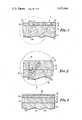
- FIG. 1is a cross-sectional view of a form of the low-cost solar cell of the present invention.
- FIG. 2is an enlarged view of the encircled portion of FIG. 1.
- FIG. 3is another form of the low-cost solar cell of the present invention.
- the solar cell 10includes a thin layer of active material 12 on a substrate 14.
- the active layer 12is a semiconductor material, such as silicon, with a light incidence surface 27, an N-type region 16, a P-type region 18, and a P-N junction 20 therebetween. Region 16 can as well be of P-type and region 18 can be of N-type with no essential change in results.
- the substrate 14is of any material which is transparent to light.
- the substrate 14can be of sapphire, spinel, high temperature glass or quartz. If the substrate 14 is of sapphire of spinel, it has the advantage of permitting the epitaxial growth of the active layer 12 thereon.
- Substrate 14has two opposing surfaces, which are the flat surface 22 and the grooved surface 24.
- the active layer 12is on the flat surface 22.
- the grooved surface 24is in the form of a polished sawtooth pattern with the surface of each sawtooth at an angle ⁇ .
- On the grooved surface 24is a reflective layer 26.
- the reflective layer 26is typically of a metallic material with good light reflection characteristics.
- the solar light ray 28, falling on the active layer 12 at incident surface 27optically generates electrons and holes in the active layer 12, at the points where the light ray 28 is absorbed.
- a characteristic of silicon, which is typically of what the active layer 12 comprises,is a weak absorption for low frequency radiation.
- the spectrum of solar lightcomprises colors of varying frequencies, many of which are of a sufficiently low frequency that their radiation will penetrate deeply into an active layer of such a solar cell before it will be absorbed.
- a thick active layeris needed to assure total absorption of solar light.
- the typical solar cellhas an active layer thickness on the order of 250 microns, but in the present invention the active layer 12 is 2.5 microns or less in thickness.
- the ability to use this reduction in active layer thicknessis the result of the grooved surface 24 and reflective layer 26.
- portions of the light ray 28 having low frequencieswill tend to penetrate active layer 12 without being absorbed. However, they will not penetrate reflective layer 26 and are reflected back into the active layer 12 of the solar cell 10.
- the reflected ray 28(a)can be made to undergo total internal reflection upon reaching the incident surface 27. This retains the reflected ray 28(a) within the solar cell 10, giving it multiple opportunities to be absorbed by the active layer 12.
- the ray 28(a)must fall on incident surface 27 at an angle of incidence greater than the critical angle ⁇ c .
- the critical angleis calculated by the following formula:
- n 1is the absolute index of refraction for the first medium through which the light passes
- n ois the absolute index of refraction of the second medium to which the light, if totally internally reflected, will not pass. Therefore, if the active layer 12 comprises the material silicon, whose index of refraction n 1 is 3.5, and the second medium is air, whose index of refraction n 0 is 1, the critical angle is approximately 17°. Any reflected light ray emerging toward incident surface 27 at an angle greater than 17° will be totally internally reflected back into the solar cell 10.
- achieving total internal reflection of the reflected light ray 28(a)is dependent, in the present invention, on the angle ⁇ of the reflective layer 26.
- the surface of the sawteeth forming the grooved surface 24are at an angle ⁇ and, therefore, the reflective layer 26 on the grooved surface 24 will be at an angle ⁇ with respect to light ray 28.
- the light ray 28reflects off the layer 26, its direction changes by an angle twice the value of angle ⁇ .
- a perpendicular line 30 drawn to the reflective layer 26illustrates that the light ray 28 falls on the reflective surface at an angle of incidence, i 1 , equal to ⁇ and is reflected from the reflective layer 26 by an angle of reflection, r 1 , also equal to ⁇ , thus, the total angle at which the light ray 28 has been reflected is 2 ⁇ .
- the reflected light ray 28(a)will strike the flat surface 22 at an angle of incidence i 2 equal to 2 ⁇ .
- the angle of refractiondesignated r 2
- i 2is the angle of incidence of the reflected ray 28(a) and is equal to 2 ⁇ in the present invention
- r 2is the angle of refraction of the reflected ray 28(a)
- n ACTIVEis the index of refraction of the active layer 12
- n SUBis the index of refraction of the substrate 14.
- the angle of refraction, r 2is the angle at which the reflected light ray 28(a) will strike the incident surface 27, and if this angle is greater than the critical angle ⁇ c , calculated by formula 1, total internal reflection will occur. Therefore, by properly selecting the angle ⁇ of the grooved surface 24 and reflecting layer 26, total internal reflection of light is possible.
- the reflected ray 28(a)After the reflected ray 28(a) has been reflected back from the incident surface 27, it will continue being reflected through the solar cell 10 for a finite number of times. Each time it is reflected off of the incident surface 27 it causes two more traversals of the active layer 12, thus increasing the opportunity for absorption.
- the finite number of passes which the light ray makes through the solar devicesimulates the absorption of a light ray travelling through a solar cell with a much thicker active layer.
- the active layer 12is very thin. This makes it possible for minority carriers with a short lifetime to diffuse to the junction 20. A lifetime as much as 1000 times lower than that of conventional solar cells can be tolerated in the present invention. Since a short minority carrier lifetime is tolerable, the active layer can be composed of a material of lower quality, possibly even polycrystalline silicon, instead of the higher quality single crystalline silicon. Therefore, the cost of the present invention is lower than the cost of conventional silicon solar cells, because only a thin active layer is needed, saving substantially on the quantity of the active layer, and because the active semiconductor material composing the active layer can be of a lower quality than is normally required.
- the substrateis noncrystalline, such as a high-temperature glass or quartz.
- a glass or quartz substratewill tend to be less costly than a substrate of sapphire, although the active layer 12 can be epitaxially grown onto a sapphire substrate.
- An important advantage that results from the use of a very thin layer of active material in the present inventionis that low cost substrate material, such as glass or quartz, can have a thin layer of active material of adequate quality deposited on it, but a thick layer of active material deposited on a low cost substrate will be of unacceptable quality.
- a single crystalline active layer 12can be deposited on the flat surface 22 of a sapphire or spinel substrate 14 by a variety of well known deposition means such as described in U.S. Pat. No. 3,658,586, issued Apr. 25, 1972 to C. C. Wang.
- a thin layer of polycrystalline siliconcan be deposited on a low cost substrate material by a process such as described in the article, "Low Temperature Growth and Properties of Polycrystalline Silicon,” by Y. S. Chiang, SEMICONDUCTOR SILICON 1973, edited by H. R. Huff and R. R. Burgess, Electrochemical Society (Princeton, N.J. 1973), pages 285-291.
- a P-N junctionis formed in the active layer 12 by using any of a variety of junction-forming processes such as ion implantation for the introduction of doping impurities to form region 16.
- the forming of grooved surface 24 in the substrate 14is accomplished by standard polishing techniques, if the substrate 14 is sapphire. If the substrate 14 is a high-temperature glass or quartz, the grooved surface 24 may be molded into the substrate 14. After the grooved surface 24 is formed, a metallic material is deposited on the grooved surface 24 to form the reflective layer 26.
- a second embodiment of the solar cell of the present invention shown thereinis designated as 110.
- the solar cell 110is similar in structure to the prior embodiment of the solar cell designated as 10 and shown in FIG. 1.
- the solar cell 110includes a thin active layer 112 and a substrate 114.
- Active layer 112is the same as active layer 12.
- Active layer 112includes an N-type region 116 and a P-type region 118 which are the same as regions 16 and 18 respectively of solar cell 10.
- the substrate 114has two transparent regions. One region is a deposition region 132.
- the active layer 112is on the deposition region 132 at a flat surface 122.
- the flat surface 122is the same as flat surface 22.
- the reflector region 134In contact with the deposition region 132 is the reflector region 134, forming a boundary 136 therebetween.
- Opposite boundary 136is a grooved surface 124 upon which is the reflective layer 126. Grooved surface 124 and reflective layer 126 are the same as grooved surface 24 and reflective layer 26, respectively.
- the deposition region 132is of a transparent material, which is compatible with nucleation of the growth of the active layer 112 on the deposition region 132 at the flat surface 122.
- the deposition region 132can be of high-temperature glass, quartz, sapphire or spinel.
- the reflector region 134is of a glass or plastic material.
- the deposition region 132may be bonded to the reflector region 134, at the boundary 136, with a bonding material transparent to light.
- the substrate 14could be a plastic. This was because most processes for depositing the active layer semiconductor material on the substrate require heat that would distort plastic.
- the reflector region 136can be plastic since little or no heat is needed in the bonding process.
- the active layer 112is deposited on the substrate 114, but a cost savings results from the use of a smaller amount of nucleating material which is generally more expensive than the materials comprising the reflector region 136.
- An additional cost savingsresults since grooves are easily molded into a glass or plastic reflector region 136. For other materials such as sapphire, grooves can only be formed in the material by a more expensive polishing process.
- the second embodimentis lower in cost since only a small amount of low quality semiconductor material is needed for the active region 112.
- the present inventionprovides a lowcost solar cell because a lesser amount of the active layer material is needed, it can be of a lower quality, and the substrate is of a lesser amount of expensive nucleating material.
Landscapes
- Photovoltaic Devices (AREA)
Abstract
Description
The present invention relates to solar cells. More specifically, the present invention relates to solar cells with a very thin layer of active material on a surface of a transparent substrate whose opposite surface is grooved at a certain angle, and on which is a layer of reflective material.
In the past it was not the practice in making solar cells of materials like silicon to use thin layers of active material because it resulted in a severe loss in solar cell light absorption.
The loss of light absorption is due to the fact that for the active material, typically silicon, the longer the wavelength of the incident light, the weaker the active material's light absorption. If absorption is weak, the incident light will penetrate through the active material and not be absorbed. To assure absorption of that portion of the solar spectrum consisting of long wavelength radiation, a thick layer of active material was needed. Once the light has been absorbed in the active material, an electron-hole pair is generated. To assure that the lifetime of the generated minority carrier, be it a hole or an electron, was sufficient for the generation of current, the active material had to be of a high quality. In other words, the lifetime of the generated carrier is a dominant factor in determining the diffusion length of carriers generated in the active material. Diffusion length is the average distance a carrier can travel before it recombines. Since a thick layer of active material was required for absorption, a diffusion length at least as great as the active layer thickness was needed to assure current generation by the carriers formed deep in the active layer. Therefore, in the past, a solar cell consisted of a thick layer of highly pure active material.
If a thinner layer of active material could be used, a lower-cost solar cell would result for two reasons. First, a thin layer of active material would greatly reduce the required amount of active material, which is costly. Secondly, a thin layer of active material would require a proportionally shorter diffusion length for optically generated electrons and holes. The ability to use shorter diffusion lengths would allow the use of active material of lower quality, an additional cost saving. Therefore, a much desired need is a solar cell with a thin layer of moderate purity active material with little loss in solar light absorption.
A solar cell including a transparent substrate having a pair of opposed surfaces. An active layer of semiconductor material having a surface of incidence is on one surface of the substrate. Grooves are in the other surface of the substrate and a reflective layer is on the surface of the grooves.
FIG. 1 is a cross-sectional view of a form of the low-cost solar cell of the present invention.
FIG. 2 is an enlarged view of the encircled portion of FIG. 1.
FIG. 3 is another form of the low-cost solar cell of the present invention.
Referring to FIG. 1, a form of the low-cost solar cell is designated at 10. Thesolar cell 10 includes a thin layer ofactive material 12 on asubstrate 14.
Theactive layer 12 is a semiconductor material, such as silicon, with alight incidence surface 27, an N-type region 16, a P-type region 18, and aP-N junction 20 therebetween.Region 16 can as well be of P-type andregion 18 can be of N-type with no essential change in results.
Thesubstrate 14 is of any material which is transparent to light. For example, thesubstrate 14 can be of sapphire, spinel, high temperature glass or quartz. If thesubstrate 14 is of sapphire of spinel, it has the advantage of permitting the epitaxial growth of theactive layer 12 thereon.
Thesolar light ray 28, falling on theactive layer 12 atincident surface 27 optically generates electrons and holes in theactive layer 12, at the points where thelight ray 28 is absorbed. A characteristic of silicon, which is typically of what theactive layer 12 comprises, is a weak absorption for low frequency radiation. The spectrum of solar light comprises colors of varying frequencies, many of which are of a sufficiently low frequency that their radiation will penetrate deeply into an active layer of such a solar cell before it will be absorbed. A thick active layer is needed to assure total absorption of solar light.
The typical solar cell has an active layer thickness on the order of 250 microns, but in the present invention theactive layer 12 is 2.5 microns or less in thickness. The ability to use this reduction in active layer thickness is the result of thegrooved surface 24 andreflective layer 26.
In the present invention, portions of thelight ray 28 having low frequencies will tend to penetrateactive layer 12 without being absorbed. However, they will not penetratereflective layer 26 and are reflected back into theactive layer 12 of thesolar cell 10. By the proper choice of the angle α, the reflected ray 28(a) can be made to undergo total internal reflection upon reaching theincident surface 27. This retains the reflected ray 28(a) within thesolar cell 10, giving it multiple opportunities to be absorbed by theactive layer 12.
According to Snell's Law, which is well known in the art, to achieve total internal reflection of the ray 28(a), the ray 28(a) must fall onincident surface 27 at an angle of incidence greater than the critical angle θc. The critical angle is calculated by the following formula:
1. sin θ.sub.c = n.sub.0 /n.sub.1
where n1 is the absolute index of refraction for the first medium through which the light passes, and no is the absolute index of refraction of the second medium to which the light, if totally internally reflected, will not pass. Therefore, if theactive layer 12 comprises the material silicon, whose index of refraction n1 is 3.5, and the second medium is air, whose index of refraction n0 is 1, the critical angle is approximately 17°. Any reflected light ray emerging towardincident surface 27 at an angle greater than 17° will be totally internally reflected back into thesolar cell 10.
Referring to FIG. 2, achieving total internal reflection of the reflected light ray 28(a) is dependent, in the present invention, on the angle α of thereflective layer 26. The surface of the sawteeth forming thegrooved surface 24 are at an angle α and, therefore, thereflective layer 26 on thegrooved surface 24 will be at an angle α with respect tolight ray 28. It is a principle of light reflection, well known in the art, that a ray of light reflected by a reflective surface will have an angle of incidence equal to the angle of reflection. When thelight ray 28 reflects off thelayer 26, its direction changes by an angle twice the value of angle α. Aperpendicular line 30 drawn to thereflective layer 26 illustrates that thelight ray 28 falls on the reflective surface at an angle of incidence, i1, equal to α and is reflected from thereflective layer 26 by an angle of reflection, r1, also equal to α, thus, the total angle at which thelight ray 28 has been reflected is 2 α.
According to the basic principles of geometry, the reflected light ray 28(a) will strike theflat surface 22 at an angle of incidence i2 equal to 2 α. By then utilizing Snell's Law the angle of refraction, designated r2, as the reflected ray 28(a) passes from thesubstrate 14 to theactive layer 12 can be calculated. The formula used to make this calculation is as follows: ##EQU1## wherein i2 is the angle of incidence of the reflected ray 28(a) and is equal to 2 α in the present invention, r2 is the angle of refraction of the reflected ray 28(a), nACTIVE is the index of refraction of theactive layer 12 and nSUB is the index of refraction of thesubstrate 14. Again, according to basic principles of geometry, the angle of refraction, r2, is the angle at which the reflected light ray 28(a) will strike theincident surface 27, and if this angle is greater than the critical angle θc, calculated by formula 1, total internal reflection will occur. Therefore, by properly selecting the angle α of thegrooved surface 24 and reflectinglayer 26, total internal reflection of light is possible.
After the reflected ray 28(a) has been reflected back from theincident surface 27, it will continue being reflected through thesolar cell 10 for a finite number of times. Each time it is reflected off of theincident surface 27 it causes two more traversals of theactive layer 12, thus increasing the opportunity for absorption. The finite number of passes which the light ray makes through the solar device simulates the absorption of a light ray travelling through a solar cell with a much thicker active layer.
Once the light has been absorbed in the active layer 12 a hole-electron pair is generated. The minority carriers optically generated in both the P-type region 18 and the N-type region 16 diffuse toward theP-N junction 20. Current is generated by thesolar cell 10 only when the minority carriers, with sufficiently long lifetimes, diffuse to thejunction 20. The lifetime of a minority carrier is the mean time it can travel in a majority region and remain a free charge. A long minority carrier lifetime requires the material composing the active layer to be very pure.
In the present invention theactive layer 12 is very thin. This makes it possible for minority carriers with a short lifetime to diffuse to thejunction 20. A lifetime as much as 1000 times lower than that of conventional solar cells can be tolerated in the present invention. Since a short minority carrier lifetime is tolerable, the active layer can be composed of a material of lower quality, possibly even polycrystalline silicon, instead of the higher quality single crystalline silicon. Therefore, the cost of the present invention is lower than the cost of conventional silicon solar cells, because only a thin active layer is needed, saving substantially on the quantity of the active layer, and because the active semiconductor material composing the active layer can be of a lower quality than is normally required.
An additional cost saving will result if the substrate is noncrystalline, such as a high-temperature glass or quartz. A glass or quartz substrate will tend to be less costly than a substrate of sapphire, although theactive layer 12 can be epitaxially grown onto a sapphire substrate. An important advantage that results from the use of a very thin layer of active material in the present invention is that low cost substrate material, such as glass or quartz, can have a thin layer of active material of adequate quality deposited on it, but a thick layer of active material deposited on a low cost substrate will be of unacceptable quality.
In the first embodiment of the present invention shown in FIG. 1, a single crystallineactive layer 12 can be deposited on theflat surface 22 of a sapphire orspinel substrate 14 by a variety of well known deposition means such as described in U.S. Pat. No. 3,658,586, issued Apr. 25, 1972 to C. C. Wang. A thin layer of polycrystalline silicon can be deposited on a low cost substrate material by a process such as described in the article, "Low Temperature Growth and Properties of Polycrystalline Silicon," by Y. S. Chiang, SEMICONDUCTOR SILICON 1973, edited by H. R. Huff and R. R. Burgess, Electrochemical Society (Princeton, N.J. 1973), pages 285-291. A P-N junction is formed in theactive layer 12 by using any of a variety of junction-forming processes such as ion implantation for the introduction of doping impurities to formregion 16. The forming of groovedsurface 24 in thesubstrate 14 is accomplished by standard polishing techniques, if thesubstrate 14 is sapphire. If thesubstrate 14 is a high-temperature glass or quartz, thegrooved surface 24 may be molded into thesubstrate 14. After thegrooved surface 24 is formed, a metallic material is deposited on thegrooved surface 24 to form thereflective layer 26.
Referring to FIG. 3, a second embodiment of the solar cell of the present invention shown therein is designated as 110. Thesolar cell 110 is similar in structure to the prior embodiment of the solar cell designated as 10 and shown in FIG. 1. Thesolar cell 110 includes a thinactive layer 112 and asubstrate 114.Active layer 112 is the same asactive layer 12.Active layer 112 includes an N-type region 116 and a P-type region 118 which are the same asregions solar cell 10.
In this embodiment thesubstrate 114 has two transparent regions. One region is adeposition region 132. Theactive layer 112 is on thedeposition region 132 at aflat surface 122. Theflat surface 122 is the same asflat surface 22. In contact with thedeposition region 132 is thereflector region 134, forming aboundary 136 therebetween. Oppositeboundary 136 is agrooved surface 124 upon which is thereflective layer 126.Grooved surface 124 andreflective layer 126 are the same as groovedsurface 24 andreflective layer 26, respectively.
Thedeposition region 132 is of a transparent material, which is compatible with nucleation of the growth of theactive layer 112 on thedeposition region 132 at theflat surface 122. Thedeposition region 132 can be of high-temperature glass, quartz, sapphire or spinel. Thereflector region 134 is of a glass or plastic material.
Thedeposition region 132 may be bonded to thereflector region 134, at theboundary 136, with a bonding material transparent to light.
In the prior embodiment of the present invention there was no suggestion that thesubstrate 14 could be a plastic. This was because most processes for depositing the active layer semiconductor material on the substrate require heat that would distort plastic. In the second embodiment of thesolar cell 110, thereflector region 136 can be plastic since little or no heat is needed in the bonding process.
In the second embodiment of the present invention, theactive layer 112 is deposited on thesubstrate 114, but a cost savings results from the use of a smaller amount of nucleating material which is generally more expensive than the materials comprising thereflector region 136. An additional cost savings results since grooves are easily molded into a glass orplastic reflector region 136. For other materials such as sapphire, grooves can only be formed in the material by a more expensive polishing process. As in the first embodiment of the solar cell, the second embodiment is lower in cost since only a small amount of low quality semiconductor material is needed for theactive region 112.
Therefore, the present invention provides a lowcost solar cell because a lesser amount of the active layer material is needed, it can be of a lower quality, and the substrate is of a lesser amount of expensive nucleating material.
Claims (9)
1. A solar cell comprising a substrate transparent to solar light having a pair of opposed surfaces, an active layer of silicon semiconductor material on one surface of said substrate, said active layer having a surface of incidence, grooves in the other surface of said substrate, means for reflecting solar light at the surface of the grooves, said active layer being no greater than about 2.5 microns in thickness.
2. The solar cell in accordance with claim 1 in which said grooves are in the form of a sawtooth pattern.
3. The solar cell in accordance with claim 2 in which said surface of the grooves are at an angle such that light reflected from said reflective means will strike said incident surface at such an angle as to be totally internally reflected.
4. The solar cell in accordance with claim 1 in which said active layer has an N-type and a P-type conductivity region and a P-N junction therebetween.
5. The solar cell in accordance with claim 1 in which said substrate is of a transparent material selected from the group consisting of high-temperature glass, quartz, sapphire and spinel.
6. The solar cell in accordance with claim 1 in which said substrate has a deposition region contiguous to said active layer, which is of a material that will nucleate the growth of said active layer, and a reflector region in contact with said deposition region.
7. The solar cell in accordance with claim 6 in which said deposition region is of a transparent material selected from the group consisting of high-temperature glass, quartz, sapphire and spinel.
8. The solar cell in accordance with claim 6 in which said reflector region is of a transparent material selected from the group consisting of plastics and glass.
9. The solar cell in accordance with claim 3 in which said reflective means is a reflective layer on the surface of said grooves.
Priority Applications (8)
| Application Number | Priority Date | Filing Date | Title |
|---|---|---|---|
| US05/450,000US3973994A (en) | 1974-03-11 | 1974-03-11 | Solar cell with grooved surface |
| CA220,006ACA1021445A (en) | 1974-03-11 | 1975-02-13 | Low-cost solar cell device |
| AU78802/75AAU488420B2 (en) | 1974-03-11 | 1975-03-05 | Low-cost solar cell device |
| GB9150/75AGB1489318A (en) | 1974-03-11 | 1975-03-05 | Low-cost solar cell device |
| DE19752509533DE2509533A1 (en) | 1974-03-11 | 1975-03-05 | SUN CELL |
| FR7507166AFR2264399B1 (en) | 1974-03-11 | 1975-03-07 | |
| JP50029455AJPS50123286A (en) | 1974-03-11 | 1975-03-10 | |
| JP1977072473UJPS52159173U (en) | 1974-03-11 | 1977-06-02 |
Applications Claiming Priority (1)
| Application Number | Priority Date | Filing Date | Title |
|---|---|---|---|
| US05/450,000US3973994A (en) | 1974-03-11 | 1974-03-11 | Solar cell with grooved surface |
Publications (1)
| Publication Number | Publication Date |
|---|---|
| US3973994Atrue US3973994A (en) | 1976-08-10 |
Family
ID=23786349
Family Applications (1)
| Application Number | Title | Priority Date | Filing Date |
|---|---|---|---|
| US05/450,000Expired - LifetimeUS3973994A (en) | 1974-03-11 | 1974-03-11 | Solar cell with grooved surface |
Country Status (6)
| Country | Link |
|---|---|
| US (1) | US3973994A (en) |
| JP (2) | JPS50123286A (en) |
| CA (1) | CA1021445A (en) |
| DE (1) | DE2509533A1 (en) |
| FR (1) | FR2264399B1 (en) |
| GB (1) | GB1489318A (en) |
Cited By (85)
| Publication number | Priority date | Publication date | Assignee | Title |
|---|---|---|---|---|
| US4116718A (en)* | 1978-03-09 | 1978-09-26 | Atlantic Richfield Company | Photovoltaic array including light diffuser |
| US4143234A (en)* | 1976-11-08 | 1979-03-06 | Monsanto Company | Solar collector using total internal reflectance |
| US4162928A (en)* | 1978-09-29 | 1979-07-31 | Nasa | Solar cell module |
| US4166919A (en)* | 1978-09-25 | 1979-09-04 | Rca Corporation | Amorphous silicon solar cell allowing infrared transmission |
| US4235643A (en)* | 1978-06-30 | 1980-11-25 | Exxon Research & Engineering Co. | Solar cell module |
| US4253882A (en)* | 1980-02-15 | 1981-03-03 | University Of Delaware | Multiple gap photovoltaic device |
| EP0029721A1 (en)* | 1979-11-26 | 1981-06-03 | Exxon Research And Engineering Company | Solar cell modules |
| EP0042458A1 (en)* | 1980-05-20 | 1981-12-30 | Solarex Corporation | Solar cell module and method of increasing the output current of said module |
| US4313023A (en)* | 1979-02-28 | 1982-01-26 | Exxon Research & Engineering Co. | Solar cell module |
| US4321417A (en)* | 1978-06-30 | 1982-03-23 | Exxon Research & Engineering Co. | Solar cell modules |
| US4360701A (en)* | 1981-05-15 | 1982-11-23 | The United States Of America As Represented By The Administrator Of The National Aeronautics And Space Administration | Heat transparent high intensity high efficiency solar cell |
| US4377723A (en)* | 1980-05-02 | 1983-03-22 | The University Of Delaware | High efficiency thin-film multiple-gap photovoltaic device |
| US4398056A (en)* | 1981-07-23 | 1983-08-09 | Exxon Research And Engineering Co. | Solar cell with reflecting grating substrate |
| FR2522880A1 (en)* | 1982-03-03 | 1983-09-09 | Energy Conversion Devices Inc | PHOTOVOLTAIC DEVICE COMPRISING MEANS FOR DIRECTING INCIDENT RADIATION FOR TOTAL INTERNAL REFLECTION |
| EP0102204A1 (en)* | 1982-08-04 | 1984-03-07 | Exxon Research And Engineering Company | An optically enhanced photovoltaic device |
| US4497974A (en)* | 1982-11-22 | 1985-02-05 | Exxon Research & Engineering Co. | Realization of a thin film solar cell with a detached reflector |
| EP0106540A3 (en)* | 1982-09-17 | 1985-06-05 | Exxon Research And Engineering Company | Thin film semi-conductor device with enhanced optical absorption properties, and method of making same |
| US4571448A (en)* | 1981-11-16 | 1986-02-18 | University Of Delaware | Thin film photovoltaic solar cell and method of making the same |
| EP0117061A3 (en)* | 1983-01-18 | 1986-07-23 | Exxon Research And Engineering Company | Improved solar cell |
| US4674244A (en)* | 1986-07-17 | 1987-06-23 | Single-Ply Institute Of America, Inc. | Roof construction having insulation structure, membrane and photovoltaic cells |
| US4818337A (en)* | 1986-04-11 | 1989-04-04 | University Of Delaware | Thin active-layer solar cell with multiple internal reflections |
| DE4124795A1 (en)* | 1990-07-27 | 1992-02-20 | Fraunhofer Ges Forschung | Solar panel with prismatic glass ridges - uses triangular surfaces at optimum angle for internal reflection |
| US5228926A (en)* | 1990-09-20 | 1993-07-20 | United Solar Systems Corporation | Photovoltaic device with increased light absorption and method for its manufacture |
| US5232519A (en)* | 1990-09-20 | 1993-08-03 | United Solar Systems Corporation | Wireless monolithic photovoltaic module |
| US5261970A (en)* | 1992-04-08 | 1993-11-16 | Sverdrup Technology, Inc. | Optoelectronic and photovoltaic devices with low-reflectance surfaces |
| US6008449A (en)* | 1997-08-19 | 1999-12-28 | Cole; Eric D. | Reflective concentrating solar cell assembly |
| EP1043779A3 (en)* | 1999-04-05 | 2001-05-02 | Sony Corporation | Thin film solar battery and method of manufacturing the same |
| WO2001039280A1 (en)* | 1999-11-26 | 2001-05-31 | The Trustees Of Princeton University | Highly efficient multiple reflection photosensitive optoelectronic device with optical concentrator |
| US20020119297A1 (en)* | 1998-08-19 | 2002-08-29 | Forrest Stephen R. | Organic photosensitive optoelectronic devices with transparent electrodes |
| US20040035460A1 (en)* | 2002-06-12 | 2004-02-26 | Gonsiorawski Ronald C. | Photovoltaic module with light reflecting backskin |
| US6738139B1 (en) | 2002-08-26 | 2004-05-18 | J.A. Woollam Co., Inc. | Method of determining bulk refractive indicies of fluids from thin films thereof |
| US20040151887A1 (en)* | 1998-08-19 | 2004-08-05 | Forrest Stephen R. | Method of fabricating an organic photosensitive optoelectronic device with an exciton blocking layer |
| US20060231133A1 (en)* | 2005-04-19 | 2006-10-19 | Palo Alto Research Center Incorporated | Concentrating solar collector with solid optical element |
| US20070016963A1 (en)* | 2005-07-14 | 2007-01-18 | Xac Automation Corp. | PIN entry terminal having security system |
| US20070108229A1 (en)* | 2005-11-17 | 2007-05-17 | Palo Alto Research Center Incorporated | Extrusion/dispensing systems and methods |
| US20070110836A1 (en)* | 2005-11-17 | 2007-05-17 | Palo Alto Research Center Incorporated | Extrusion/dispensing systems and methods |
| US20070169806A1 (en)* | 2006-01-20 | 2007-07-26 | Palo Alto Research Center Incorporated | Solar cell production using non-contact patterning and direct-write metallization |
| US20070251568A1 (en)* | 2006-04-26 | 2007-11-01 | Palo Alto Research Center Incorporated | Beam Integration For Concentrating Solar Collector |
| US20070256726A1 (en)* | 2006-05-05 | 2007-11-08 | Palo Alto Research Center Incorporated | Laminated Solar Concentrating Photovoltaic Device |
| US20070256724A1 (en)* | 2006-05-05 | 2007-11-08 | Palo Alto Research Center Incorporated | Passively Cooled Solar Concentrating Photovoltaic Device |
| US20080099952A1 (en)* | 2006-11-01 | 2008-05-01 | Palo Alto Research Center Incorporated | Extrusion Head With Planarized Edge Surface |
| US20080102558A1 (en)* | 2006-11-01 | 2008-05-01 | Palo Alto Research Center Incorporated | Closely Spaced, High-Aspect Extruded Gridlines |
| US20080099953A1 (en)* | 2006-11-01 | 2008-05-01 | Palo Alto Research Center Incorporated | Extruded Structure With Equilibrium Shape |
| US20080116182A1 (en)* | 2006-11-21 | 2008-05-22 | Palo Alto Research Center Incorporated | Multiple Station Scan Displacement Invariant Laser Ablation Apparatus |
| US20080116183A1 (en)* | 2006-11-21 | 2008-05-22 | Palo Alto Research Center Incorporated | Light Scanning Mechanism For Scan Displacement Invariant Laser Ablation Apparatus |
| US20080138999A1 (en)* | 2006-12-12 | 2008-06-12 | Palo Alto Research Center Incorporated | Solar Cell Fabrication Using Extrusion Mask |
| US20080186593A1 (en)* | 2007-02-02 | 2008-08-07 | Sol Focus, Inc. | Metal trace fabrication for optical element |
| US20080277885A1 (en)* | 2007-05-08 | 2008-11-13 | Palo Alto Research Center Incorporated | Wiring-Free, Plumbing-Free, Cooled, Vacuum Chuck |
| US20090101201A1 (en)* | 2007-10-22 | 2009-04-23 | White John M | Nip-nip thin-film photovoltaic structure |
| US20090266399A1 (en)* | 2008-04-28 | 2009-10-29 | Basol Bulent M | Metallic foil substrate and packaging technique for thin film solar cells and modules |
| US20090269877A1 (en)* | 2008-04-28 | 2009-10-29 | Mustafa Pinarbasi | Method and apparatus for achieving low resistance contact to a metal based thin film solar cell |
| US20090266398A1 (en)* | 2008-04-28 | 2009-10-29 | Burak Metin | Method and Apparatus to Form Back Contacts to Flexible CIGS Solar Cells |
| US20100059109A1 (en)* | 2008-09-09 | 2010-03-11 | Palo Alto Research Center Incorporated | Interdigitated Back Contact Silicon Solar Cells With Laser Ablated Grooves |
| US20100117254A1 (en)* | 2008-11-07 | 2010-05-13 | Palo Alto Research Center Incorporated | Micro-Extrusion System With Airjet Assisted Bead Deflection |
| US20100118081A1 (en)* | 2008-11-07 | 2010-05-13 | Palo Alto Research Center Incorporated | Dead Volume Removal From An Extrusion Printhead |
| US20100124619A1 (en)* | 2008-11-14 | 2010-05-20 | Palo Alto Research Center Incorporated | Solar cell metallization using inline electroless plating |
| US20100278480A1 (en)* | 2009-04-21 | 2010-11-04 | Vasylyev Sergiy V | Light collection and illumination systems employing planar waveguide |
| US20100313933A1 (en)* | 2008-02-21 | 2010-12-16 | Jianguo Xu | Reflector-solar receiver assembly and solar module |
| US20100330726A1 (en)* | 2003-06-10 | 2010-12-30 | Gonsiorawski Ronald C | Photovoltaic module with light reflecting backskin |
| US20110083728A1 (en)* | 2009-10-14 | 2011-04-14 | Palo Alto Research Center Incorporated | Disordered Nanowire Solar Cell |
| US7928015B2 (en) | 2006-12-12 | 2011-04-19 | Palo Alto Research Center Incorporated | Solar cell fabrication using extruded dopant-bearing materials |
| US20110100419A1 (en)* | 2009-11-03 | 2011-05-05 | Palo Alto Research Center Incorporated | Linear Concentrating Solar Collector With Decentered Trough-Type Relectors |
| US20110100418A1 (en)* | 2009-11-03 | 2011-05-05 | Palo Alto Research Center Incorporated | Solid Linear Solar Concentrator Optical System With Micro-Faceted Mirror Array |
| WO2011065571A1 (en)* | 2009-11-30 | 2011-06-03 | 京セラ株式会社 | Photoelectric conversion module, method for manufacturing same, and power generation device |
| US20110216401A1 (en)* | 2010-03-03 | 2011-09-08 | Palo Alto Research Center Incorporated | Scanning System With Orbiting Objective |
| US8080729B2 (en) | 2008-11-24 | 2011-12-20 | Palo Alto Research Center Incorporated | Melt planarization of solar cell bus bars |
| US8117983B2 (en) | 2008-11-07 | 2012-02-21 | Solarworld Innovations Gmbh | Directional extruded bead control |
| US8226391B2 (en) | 2006-11-01 | 2012-07-24 | Solarworld Innovations Gmbh | Micro-extrusion printhead nozzle with tapered cross-section |
| US8399283B2 (en) | 2005-11-17 | 2013-03-19 | Solarworld Innovations Gmbh | Bifacial cell with extruded gridline metallization |
| US20140197509A1 (en)* | 2009-09-17 | 2014-07-17 | Sionyx, Inc. | Photosensitive imaging devices and associated methods |
| US8846431B2 (en) | 2011-03-03 | 2014-09-30 | Palo Alto Research Center Incorporated | N-type silicon solar cell with contact/protection structures |
| US8960120B2 (en) | 2008-12-09 | 2015-02-24 | Palo Alto Research Center Incorporated | Micro-extrusion printhead with nozzle valves |
| US9496308B2 (en) | 2011-06-09 | 2016-11-15 | Sionyx, Llc | Process module for increasing the response of backside illuminated photosensitive imagers and associated methods |
| US9673250B2 (en) | 2013-06-29 | 2017-06-06 | Sionyx, Llc | Shallow trench textured regions and associated methods |
| US9741761B2 (en) | 2010-04-21 | 2017-08-22 | Sionyx, Llc | Photosensitive imaging devices and associated methods |
| US9762830B2 (en) | 2013-02-15 | 2017-09-12 | Sionyx, Llc | High dynamic range CMOS image sensor having anti-blooming properties and associated methods |
| US9761739B2 (en) | 2010-06-18 | 2017-09-12 | Sionyx, Llc | High speed photosensitive devices and associated methods |
| US9905599B2 (en) | 2012-03-22 | 2018-02-27 | Sionyx, Llc | Pixel isolation elements, devices and associated methods |
| US9911781B2 (en) | 2009-09-17 | 2018-03-06 | Sionyx, Llc | Photosensitive imaging devices and associated methods |
| US9939251B2 (en) | 2013-03-15 | 2018-04-10 | Sionyx, Llc | Three dimensional imaging utilizing stacked imager devices and associated methods |
| US10244188B2 (en) | 2011-07-13 | 2019-03-26 | Sionyx, Llc | Biometric imaging devices and associated methods |
| US10361083B2 (en) | 2004-09-24 | 2019-07-23 | President And Fellows Of Harvard College | Femtosecond laser-induced formation of submicrometer spikes on a semiconductor substrate |
| US10374109B2 (en) | 2001-05-25 | 2019-08-06 | President And Fellows Of Harvard College | Silicon-based visible and near-infrared optoelectric devices |
| US20190273098A1 (en)* | 2018-03-02 | 2019-09-05 | Boe Technology Group Co., Ltd. | Anti-reflective substrate and method for preparing the same, array substrate and display device |
| CN119916610A (en)* | 2025-04-03 | 2025-05-02 | 惠科股份有限公司 | Display panel and display device |
Families Citing this family (11)
| Publication number | Priority date | Publication date | Assignee | Title |
|---|---|---|---|---|
| EG13199A (en)* | 1977-03-28 | 1981-06-30 | Rca Corp | A photo volataic device having increased absorption efficiency |
| DE2715471A1 (en)* | 1977-04-06 | 1978-10-19 | Siemens Ag | Solar cell with semiconductor layer - vacuum deposited on a reflecting substrate |
| JPS56152276A (en)* | 1980-04-25 | 1981-11-25 | Teijin Ltd | Solar cell made of amorphous silicon thin film |
| JPS57192085A (en)* | 1981-05-21 | 1982-11-26 | Toshiba Corp | Solar cell and manufacture thereof |
| IL67926A (en)* | 1982-03-18 | 1986-04-29 | Energy Conversion Devices Inc | Photo-voltaic device with radiation reflector means |
| JPS5994475A (en)* | 1982-11-20 | 1984-05-31 | Semiconductor Energy Lab Co Ltd | Photoelectric conversion semiconductor device |
| JPH0680837B2 (en)* | 1983-08-29 | 1994-10-12 | 通商産業省工業技術院長 | Photoelectric conversion element with extended optical path |
| JP2706113B2 (en)* | 1988-11-25 | 1998-01-28 | 工業技術院長 | Photoelectric conversion element |
| GB2451108A (en)* | 2007-07-18 | 2009-01-21 | Robert Michael Brady | Photovoltaic Device |
| US20100108133A1 (en)* | 2008-11-03 | 2010-05-06 | Venkata Adiseshaiah Bhagavatula | Thin Film Semiconductor Photovoltaic Device |
| GB2476300B (en)* | 2009-12-18 | 2012-11-07 | Eastman Kodak Co | Luminescent solar concentrator |
Citations (6)
| Publication number | Priority date | Publication date | Assignee | Title |
|---|---|---|---|---|
| US2320185A (en)* | 1942-04-03 | 1943-05-25 | Weston Electrical Instr Corp | Photoelectric cell |
| US2884508A (en)* | 1956-10-01 | 1959-04-28 | Dresser Ind | Thin metal films and method of making same |
| US2915578A (en)* | 1957-07-29 | 1959-12-01 | Rca Corp | Photovoltaic device |
| US3104188A (en)* | 1961-01-09 | 1963-09-17 | Giannini Controls Corp | Solid state solar generator |
| GB1028417A (en)* | 1962-06-08 | 1966-05-04 | Europ Des Semi Conducteurs Soc | Photovoltaic cell with high output |
| US3460240A (en)* | 1965-08-24 | 1969-08-12 | Westinghouse Electric Corp | Manufacture of semiconductor solar cells |
- 1974
- 1974-03-11USUS05/450,000patent/US3973994A/ennot_activeExpired - Lifetime
- 1975
- 1975-02-13CACA220,006Apatent/CA1021445A/ennot_activeExpired
- 1975-03-05DEDE19752509533patent/DE2509533A1/ennot_activeWithdrawn
- 1975-03-05GBGB9150/75Apatent/GB1489318A/ennot_activeExpired
- 1975-03-07FRFR7507166Apatent/FR2264399B1/frnot_activeExpired
- 1975-03-10JPJP50029455Apatent/JPS50123286A/jaactivePending
- 1977
- 1977-06-02JPJP1977072473Upatent/JPS52159173U/jaactivePending
Patent Citations (6)
| Publication number | Priority date | Publication date | Assignee | Title |
|---|---|---|---|---|
| US2320185A (en)* | 1942-04-03 | 1943-05-25 | Weston Electrical Instr Corp | Photoelectric cell |
| US2884508A (en)* | 1956-10-01 | 1959-04-28 | Dresser Ind | Thin metal films and method of making same |
| US2915578A (en)* | 1957-07-29 | 1959-12-01 | Rca Corp | Photovoltaic device |
| US3104188A (en)* | 1961-01-09 | 1963-09-17 | Giannini Controls Corp | Solid state solar generator |
| GB1028417A (en)* | 1962-06-08 | 1966-05-04 | Europ Des Semi Conducteurs Soc | Photovoltaic cell with high output |
| US3460240A (en)* | 1965-08-24 | 1969-08-12 | Westinghouse Electric Corp | Manufacture of semiconductor solar cells |
Non-Patent Citations (1)
| Title |
|---|
| Rahilly, "Hardened Solar Cells", in Conf. Record of the 7th Photovoltaic Conf., Pasadena, Calif., 19-21, Nov. 1968, pp. 82-84.* |
Cited By (137)
| Publication number | Priority date | Publication date | Assignee | Title |
|---|---|---|---|---|
| US4143234A (en)* | 1976-11-08 | 1979-03-06 | Monsanto Company | Solar collector using total internal reflectance |
| US4116718A (en)* | 1978-03-09 | 1978-09-26 | Atlantic Richfield Company | Photovoltaic array including light diffuser |
| US4235643A (en)* | 1978-06-30 | 1980-11-25 | Exxon Research & Engineering Co. | Solar cell module |
| US4321417A (en)* | 1978-06-30 | 1982-03-23 | Exxon Research & Engineering Co. | Solar cell modules |
| US4166919A (en)* | 1978-09-25 | 1979-09-04 | Rca Corporation | Amorphous silicon solar cell allowing infrared transmission |
| US4162928A (en)* | 1978-09-29 | 1979-07-31 | Nasa | Solar cell module |
| US4313023A (en)* | 1979-02-28 | 1982-01-26 | Exxon Research & Engineering Co. | Solar cell module |
| EP0029721A1 (en)* | 1979-11-26 | 1981-06-03 | Exxon Research And Engineering Company | Solar cell modules |
| US4253882A (en)* | 1980-02-15 | 1981-03-03 | University Of Delaware | Multiple gap photovoltaic device |
| US4377723A (en)* | 1980-05-02 | 1983-03-22 | The University Of Delaware | High efficiency thin-film multiple-gap photovoltaic device |
| EP0042458A1 (en)* | 1980-05-20 | 1981-12-30 | Solarex Corporation | Solar cell module and method of increasing the output current of said module |
| US4360701A (en)* | 1981-05-15 | 1982-11-23 | The United States Of America As Represented By The Administrator Of The National Aeronautics And Space Administration | Heat transparent high intensity high efficiency solar cell |
| US4398056A (en)* | 1981-07-23 | 1983-08-09 | Exxon Research And Engineering Co. | Solar cell with reflecting grating substrate |
| US4571448A (en)* | 1981-11-16 | 1986-02-18 | University Of Delaware | Thin film photovoltaic solar cell and method of making the same |
| FR2522880A1 (en)* | 1982-03-03 | 1983-09-09 | Energy Conversion Devices Inc | PHOTOVOLTAIC DEVICE COMPRISING MEANS FOR DIRECTING INCIDENT RADIATION FOR TOTAL INTERNAL REFLECTION |
| US4419533A (en)* | 1982-03-03 | 1983-12-06 | Energy Conversion Devices, Inc. | Photovoltaic device having incident radiation directing means for total internal reflection |
| EP0102204A1 (en)* | 1982-08-04 | 1984-03-07 | Exxon Research And Engineering Company | An optically enhanced photovoltaic device |
| EP0106540A3 (en)* | 1982-09-17 | 1985-06-05 | Exxon Research And Engineering Company | Thin film semi-conductor device with enhanced optical absorption properties, and method of making same |
| US4497974A (en)* | 1982-11-22 | 1985-02-05 | Exxon Research & Engineering Co. | Realization of a thin film solar cell with a detached reflector |
| EP0117061A3 (en)* | 1983-01-18 | 1986-07-23 | Exxon Research And Engineering Company | Improved solar cell |
| US4818337A (en)* | 1986-04-11 | 1989-04-04 | University Of Delaware | Thin active-layer solar cell with multiple internal reflections |
| US4674244A (en)* | 1986-07-17 | 1987-06-23 | Single-Ply Institute Of America, Inc. | Roof construction having insulation structure, membrane and photovoltaic cells |
| DE4124795A1 (en)* | 1990-07-27 | 1992-02-20 | Fraunhofer Ges Forschung | Solar panel with prismatic glass ridges - uses triangular surfaces at optimum angle for internal reflection |
| US5228926A (en)* | 1990-09-20 | 1993-07-20 | United Solar Systems Corporation | Photovoltaic device with increased light absorption and method for its manufacture |
| US5232519A (en)* | 1990-09-20 | 1993-08-03 | United Solar Systems Corporation | Wireless monolithic photovoltaic module |
| US5261970A (en)* | 1992-04-08 | 1993-11-16 | Sverdrup Technology, Inc. | Optoelectronic and photovoltaic devices with low-reflectance surfaces |
| US6008449A (en)* | 1997-08-19 | 1999-12-28 | Cole; Eric D. | Reflective concentrating solar cell assembly |
| US20050136232A1 (en)* | 1998-08-19 | 2005-06-23 | Forrest Stephen R. | Organic photosensitive optoelectronic device with an exciton blocking layer |
| US20040151887A1 (en)* | 1998-08-19 | 2004-08-05 | Forrest Stephen R. | Method of fabricating an organic photosensitive optoelectronic device with an exciton blocking layer |
| US20070044836A1 (en)* | 1998-08-19 | 2007-03-01 | Forrest Stephen R | Organic Photosensitive Optoelectronic Devices With Transparent Electrodes |
| US7026041B2 (en) | 1998-08-19 | 2006-04-11 | The Trustees Of Princeton University | Organic photosensitive optoelectronic device with an exciton blocking layer |
| US20020119297A1 (en)* | 1998-08-19 | 2002-08-29 | Forrest Stephen R. | Organic photosensitive optoelectronic devices with transparent electrodes |
| US8519258B2 (en) | 1998-08-19 | 2013-08-27 | The Trustees Of Princeton University | Organic photosensitive optoelectronic devices with transparent electrodes |
| US20080176098A1 (en)* | 1998-08-19 | 2008-07-24 | Forrest Stephen R | Organic photosensitive optoelectronic device with an exciton blocking layer |
| US20070045661A1 (en)* | 1998-08-19 | 2007-03-01 | Forrest Stephen R | Organic photosensitive optoelectronic device with an exciton blocking layer |
| US7151217B2 (en) | 1998-08-19 | 2006-12-19 | The Trustees Of Princeton University | Organic photosensitive optoelectronic devices with transparent electrodes |
| US7205585B2 (en) | 1998-08-19 | 2007-04-17 | The Trustees Of Princeton University | Organic photosensitive optoelectronic device with an exciton blocking layer |
| US6350945B1 (en) | 1999-04-05 | 2002-02-26 | Sony Corporation | Thin film semiconductor device and method of manufacturing the same |
| EP1043779A3 (en)* | 1999-04-05 | 2001-05-02 | Sony Corporation | Thin film solar battery and method of manufacturing the same |
| WO2001039280A1 (en)* | 1999-11-26 | 2001-05-31 | The Trustees Of Princeton University | Highly efficient multiple reflection photosensitive optoelectronic device with optical concentrator |
| US6333458B1 (en)* | 1999-11-26 | 2001-12-25 | The Trustees Of Princeton University | Highly efficient multiple reflection photosensitive optoelectronic device with optical concentrator |
| US10374109B2 (en) | 2001-05-25 | 2019-08-06 | President And Fellows Of Harvard College | Silicon-based visible and near-infrared optoelectric devices |
| US7238878B2 (en) | 2002-06-12 | 2007-07-03 | Gonsiorawski Ronald C | Photovoltaic module with light reflecting backskin |
| US20040035460A1 (en)* | 2002-06-12 | 2004-02-26 | Gonsiorawski Ronald C. | Photovoltaic module with light reflecting backskin |
| US7187443B1 (en) | 2002-08-26 | 2007-03-06 | J.A. Woollam Co., Inc. | Method of determining bulk refractive indicies of liquids from thin films thereof |
| US6738139B1 (en) | 2002-08-26 | 2004-05-18 | J.A. Woollam Co., Inc. | Method of determining bulk refractive indicies of fluids from thin films thereof |
| US20100330726A1 (en)* | 2003-06-10 | 2010-12-30 | Gonsiorawski Ronald C | Photovoltaic module with light reflecting backskin |
| US10361083B2 (en) | 2004-09-24 | 2019-07-23 | President And Fellows Of Harvard College | Femtosecond laser-induced formation of submicrometer spikes on a semiconductor substrate |
| US10741399B2 (en) | 2004-09-24 | 2020-08-11 | President And Fellows Of Harvard College | Femtosecond laser-induced formation of submicrometer spikes on a semiconductor substrate |
| US7906722B2 (en) | 2005-04-19 | 2011-03-15 | Palo Alto Research Center Incorporated | Concentrating solar collector with solid optical element |
| US20060231133A1 (en)* | 2005-04-19 | 2006-10-19 | Palo Alto Research Center Incorporated | Concentrating solar collector with solid optical element |
| US20070016963A1 (en)* | 2005-07-14 | 2007-01-18 | Xac Automation Corp. | PIN entry terminal having security system |
| US20070108229A1 (en)* | 2005-11-17 | 2007-05-17 | Palo Alto Research Center Incorporated | Extrusion/dispensing systems and methods |
| US8399283B2 (en) | 2005-11-17 | 2013-03-19 | Solarworld Innovations Gmbh | Bifacial cell with extruded gridline metallization |
| US7765949B2 (en) | 2005-11-17 | 2010-08-03 | Palo Alto Research Center Incorporated | Extrusion/dispensing systems and methods |
| US20070110836A1 (en)* | 2005-11-17 | 2007-05-17 | Palo Alto Research Center Incorporated | Extrusion/dispensing systems and methods |
| US7799371B2 (en) | 2005-11-17 | 2010-09-21 | Palo Alto Research Center Incorporated | Extruding/dispensing multiple materials to form high-aspect ratio extruded structures |
| US20070169806A1 (en)* | 2006-01-20 | 2007-07-26 | Palo Alto Research Center Incorporated | Solar cell production using non-contact patterning and direct-write metallization |
| US20070251568A1 (en)* | 2006-04-26 | 2007-11-01 | Palo Alto Research Center Incorporated | Beam Integration For Concentrating Solar Collector |
| US7855335B2 (en) | 2006-04-26 | 2010-12-21 | Palo Alto Research Center Incorporated | Beam integration for concentrating solar collector |
| US20070256724A1 (en)* | 2006-05-05 | 2007-11-08 | Palo Alto Research Center Incorporated | Passively Cooled Solar Concentrating Photovoltaic Device |
| US7851693B2 (en) | 2006-05-05 | 2010-12-14 | Palo Alto Research Center Incorporated | Passively cooled solar concentrating photovoltaic device |
| US7638708B2 (en) | 2006-05-05 | 2009-12-29 | Palo Alto Research Center Incorporated | Laminated solar concentrating photovoltaic device |
| US20070256726A1 (en)* | 2006-05-05 | 2007-11-08 | Palo Alto Research Center Incorporated | Laminated Solar Concentrating Photovoltaic Device |
| US8226391B2 (en) | 2006-11-01 | 2012-07-24 | Solarworld Innovations Gmbh | Micro-extrusion printhead nozzle with tapered cross-section |
| US7922471B2 (en) | 2006-11-01 | 2011-04-12 | Palo Alto Research Center Incorporated | Extruded structure with equilibrium shape |
| US8322025B2 (en) | 2006-11-01 | 2012-12-04 | Solarworld Innovations Gmbh | Apparatus for forming a plurality of high-aspect ratio gridline structures |
| US20080099953A1 (en)* | 2006-11-01 | 2008-05-01 | Palo Alto Research Center Incorporated | Extruded Structure With Equilibrium Shape |
| US20080099952A1 (en)* | 2006-11-01 | 2008-05-01 | Palo Alto Research Center Incorporated | Extrusion Head With Planarized Edge Surface |
| US20080102558A1 (en)* | 2006-11-01 | 2008-05-01 | Palo Alto Research Center Incorporated | Closely Spaced, High-Aspect Extruded Gridlines |
| US7780812B2 (en) | 2006-11-01 | 2010-08-24 | Palo Alto Research Center Incorporated | Extrusion head with planarized edge surface |
| US20080116183A1 (en)* | 2006-11-21 | 2008-05-22 | Palo Alto Research Center Incorporated | Light Scanning Mechanism For Scan Displacement Invariant Laser Ablation Apparatus |
| US20080116182A1 (en)* | 2006-11-21 | 2008-05-22 | Palo Alto Research Center Incorporated | Multiple Station Scan Displacement Invariant Laser Ablation Apparatus |
| US20110111076A1 (en)* | 2006-12-12 | 2011-05-12 | Palo Alto Research Center Incorporated | Solar Cell Fabrication Using Extruded Dopant-Bearing Materials |
| US7807544B2 (en) | 2006-12-12 | 2010-10-05 | Palo Alto Research Center Incorporated | Solar cell fabrication using extrusion mask |
| US7638438B2 (en) | 2006-12-12 | 2009-12-29 | Palo Alto Research Center Incorporated | Solar cell fabrication using extrusion mask |
| US7928015B2 (en) | 2006-12-12 | 2011-04-19 | Palo Alto Research Center Incorporated | Solar cell fabrication using extruded dopant-bearing materials |
| US8168545B2 (en) | 2006-12-12 | 2012-05-01 | Solarworld Innovations Gmbh | Solar cell fabrication using extruded dopant-bearing materials |
| US20080138999A1 (en)* | 2006-12-12 | 2008-06-12 | Palo Alto Research Center Incorporated | Solar Cell Fabrication Using Extrusion Mask |
| US20080186593A1 (en)* | 2007-02-02 | 2008-08-07 | Sol Focus, Inc. | Metal trace fabrication for optical element |
| US7954449B2 (en) | 2007-05-08 | 2011-06-07 | Palo Alto Research Center Incorporated | Wiring-free, plumbing-free, cooled, vacuum chuck |
| US20080277885A1 (en)* | 2007-05-08 | 2008-11-13 | Palo Alto Research Center Incorporated | Wiring-Free, Plumbing-Free, Cooled, Vacuum Chuck |
| US20090101201A1 (en)* | 2007-10-22 | 2009-04-23 | White John M | Nip-nip thin-film photovoltaic structure |
| US20100313933A1 (en)* | 2008-02-21 | 2010-12-16 | Jianguo Xu | Reflector-solar receiver assembly and solar module |
| WO2009134799A1 (en)* | 2008-04-28 | 2009-11-05 | Solopower, Inc. | Metallic foil substrate and packaging technique for thin film solar cells and modules |
| US20090266398A1 (en)* | 2008-04-28 | 2009-10-29 | Burak Metin | Method and Apparatus to Form Back Contacts to Flexible CIGS Solar Cells |
| US20090269877A1 (en)* | 2008-04-28 | 2009-10-29 | Mustafa Pinarbasi | Method and apparatus for achieving low resistance contact to a metal based thin film solar cell |
| US20090266399A1 (en)* | 2008-04-28 | 2009-10-29 | Basol Bulent M | Metallic foil substrate and packaging technique for thin film solar cells and modules |
| US8207012B2 (en) | 2008-04-28 | 2012-06-26 | Solopower, Inc. | Method and apparatus for achieving low resistance contact to a metal based thin film solar cell |
| US8426724B2 (en) | 2008-09-09 | 2013-04-23 | Palo Alto Research Center Incorporated | Interdigitated back contact silicon solar cells with separating grooves |
| US20110070681A1 (en)* | 2008-09-09 | 2011-03-24 | Palo Alto Research Center Incorporated | Interdigitated Back Contact Silicon Solar Cells With Separating Grooves |
| US7999175B2 (en) | 2008-09-09 | 2011-08-16 | Palo Alto Research Center Incorporated | Interdigitated back contact silicon solar cells with laser ablated grooves |
| US20100059109A1 (en)* | 2008-09-09 | 2010-03-11 | Palo Alto Research Center Incorporated | Interdigitated Back Contact Silicon Solar Cells With Laser Ablated Grooves |
| US9054237B2 (en) | 2008-09-09 | 2015-06-09 | Palo Alto Research Center Incorporated | Interdigitated back contact silicon solar cells fabrication using diffusion barriers |
| US20110070676A1 (en)* | 2008-09-09 | 2011-03-24 | Palo Alto Research Center Incorporated | Interdigitated Back Contact Silicon Solar Cells Fabrication Using Diffusion Barriers |
| US20100118081A1 (en)* | 2008-11-07 | 2010-05-13 | Palo Alto Research Center Incorporated | Dead Volume Removal From An Extrusion Printhead |
| US20100117254A1 (en)* | 2008-11-07 | 2010-05-13 | Palo Alto Research Center Incorporated | Micro-Extrusion System With Airjet Assisted Bead Deflection |
| US8117983B2 (en) | 2008-11-07 | 2012-02-21 | Solarworld Innovations Gmbh | Directional extruded bead control |
| US9150966B2 (en) | 2008-11-14 | 2015-10-06 | Palo Alto Research Center Incorporated | Solar cell metallization using inline electroless plating |
| US20100124619A1 (en)* | 2008-11-14 | 2010-05-20 | Palo Alto Research Center Incorporated | Solar cell metallization using inline electroless plating |
| US8080729B2 (en) | 2008-11-24 | 2011-12-20 | Palo Alto Research Center Incorporated | Melt planarization of solar cell bus bars |
| US8960120B2 (en) | 2008-12-09 | 2015-02-24 | Palo Alto Research Center Incorporated | Micro-extrusion printhead with nozzle valves |
| US9880342B2 (en) | 2009-04-21 | 2018-01-30 | Svv Technology Innovations, Inc. | Collimating illumination systems employing planar waveguide |
| US9256007B2 (en) | 2009-04-21 | 2016-02-09 | Svv Technology Innovations, Inc. | Light collection and illumination systems employing planar waveguide |
| US10627562B2 (en) | 2009-04-21 | 2020-04-21 | Svv Technology Innovations, Inc. | Illumination system using edge-lit waveguide and microstructured surfaces |
| US20100278480A1 (en)* | 2009-04-21 | 2010-11-04 | Vasylyev Sergiy V | Light collection and illumination systems employing planar waveguide |
| US10838135B2 (en) | 2009-04-21 | 2020-11-17 | Svv Technology Innovations, Inc. | Edge-lit waveguide illumination systems employing planar arrays of linear cylindrical lenses |
| US10361232B2 (en) | 2009-09-17 | 2019-07-23 | Sionyx, Llc | Photosensitive imaging devices and associated methods |
| US9911781B2 (en) | 2009-09-17 | 2018-03-06 | Sionyx, Llc | Photosensitive imaging devices and associated methods |
| US9673243B2 (en)* | 2009-09-17 | 2017-06-06 | Sionyx, Llc | Photosensitive imaging devices and associated methods |
| US20140197509A1 (en)* | 2009-09-17 | 2014-07-17 | Sionyx, Inc. | Photosensitive imaging devices and associated methods |
| US20110083728A1 (en)* | 2009-10-14 | 2011-04-14 | Palo Alto Research Center Incorporated | Disordered Nanowire Solar Cell |
| US20110100419A1 (en)* | 2009-11-03 | 2011-05-05 | Palo Alto Research Center Incorporated | Linear Concentrating Solar Collector With Decentered Trough-Type Relectors |
| US20110100418A1 (en)* | 2009-11-03 | 2011-05-05 | Palo Alto Research Center Incorporated | Solid Linear Solar Concentrator Optical System With Micro-Faceted Mirror Array |
| WO2011065571A1 (en)* | 2009-11-30 | 2011-06-03 | 京セラ株式会社 | Photoelectric conversion module, method for manufacturing same, and power generation device |
| CN102725868A (en)* | 2009-11-30 | 2012-10-10 | 京瓷株式会社 | Photoelectric conversion module, method for manufacturing same, and power generation device |
| US20110216401A1 (en)* | 2010-03-03 | 2011-09-08 | Palo Alto Research Center Incorporated | Scanning System With Orbiting Objective |
| US10229951B2 (en) | 2010-04-21 | 2019-03-12 | Sionyx, Llc | Photosensitive imaging devices and associated methods |
| US9741761B2 (en) | 2010-04-21 | 2017-08-22 | Sionyx, Llc | Photosensitive imaging devices and associated methods |
| US10505054B2 (en) | 2010-06-18 | 2019-12-10 | Sionyx, Llc | High speed photosensitive devices and associated methods |
| US9761739B2 (en) | 2010-06-18 | 2017-09-12 | Sionyx, Llc | High speed photosensitive devices and associated methods |
| US8846431B2 (en) | 2011-03-03 | 2014-09-30 | Palo Alto Research Center Incorporated | N-type silicon solar cell with contact/protection structures |
| US8962424B2 (en) | 2011-03-03 | 2015-02-24 | Palo Alto Research Center Incorporated | N-type silicon solar cell with contact/protection structures |
| US9666636B2 (en) | 2011-06-09 | 2017-05-30 | Sionyx, Llc | Process module for increasing the response of backside illuminated photosensitive imagers and associated methods |
| US10269861B2 (en) | 2011-06-09 | 2019-04-23 | Sionyx, Llc | Process module for increasing the response of backside illuminated photosensitive imagers and associated methods |
| US9496308B2 (en) | 2011-06-09 | 2016-11-15 | Sionyx, Llc | Process module for increasing the response of backside illuminated photosensitive imagers and associated methods |
| US10244188B2 (en) | 2011-07-13 | 2019-03-26 | Sionyx, Llc | Biometric imaging devices and associated methods |
| US10224359B2 (en) | 2012-03-22 | 2019-03-05 | Sionyx, Llc | Pixel isolation elements, devices and associated methods |
| US9905599B2 (en) | 2012-03-22 | 2018-02-27 | Sionyx, Llc | Pixel isolation elements, devices and associated methods |
| US9762830B2 (en) | 2013-02-15 | 2017-09-12 | Sionyx, Llc | High dynamic range CMOS image sensor having anti-blooming properties and associated methods |
| US9939251B2 (en) | 2013-03-15 | 2018-04-10 | Sionyx, Llc | Three dimensional imaging utilizing stacked imager devices and associated methods |
| US10347682B2 (en) | 2013-06-29 | 2019-07-09 | Sionyx, Llc | Shallow trench textured regions and associated methods |
| US9673250B2 (en) | 2013-06-29 | 2017-06-06 | Sionyx, Llc | Shallow trench textured regions and associated methods |
| US11069737B2 (en) | 2013-06-29 | 2021-07-20 | Sionyx, Llc | Shallow trench textured regions and associated methods |
| US20190273098A1 (en)* | 2018-03-02 | 2019-09-05 | Boe Technology Group Co., Ltd. | Anti-reflective substrate and method for preparing the same, array substrate and display device |
| US10818695B2 (en)* | 2018-03-02 | 2020-10-27 | Boe Technology Group Co., Ltd. | Anti-reflective substrate and method for preparing the same, array substrate and display device |
| CN119916610A (en)* | 2025-04-03 | 2025-05-02 | 惠科股份有限公司 | Display panel and display device |
Also Published As
| Publication number | Publication date |
|---|---|
| FR2264399B1 (en) | 1980-11-14 |
| DE2509533A1 (en) | 1975-09-18 |
| FR2264399A1 (en) | 1975-10-10 |
| JPS52159173U (en) | 1977-12-02 |
| JPS50123286A (en) | 1975-09-27 |
| CA1021445A (en) | 1977-11-22 |
| GB1489318A (en) | 1977-10-19 |
| AU7880275A (en) | 1976-09-09 |
Similar Documents
| Publication | Publication Date | Title |
|---|---|---|
| US3973994A (en) | Solar cell with grooved surface | |
| EP0747972B1 (en) | Solar cell and manufacturing method thereof | |
| US3981023A (en) | Integral lens light emitting diode | |
| US4829013A (en) | Semiconductor photoelectric conversion device, light-transparent substrate therefor and their manufacturing methods | |
| US4433202A (en) | Thin film solar cell | |
| US5066340A (en) | Photovoltaic device | |
| US4818337A (en) | Thin active-layer solar cell with multiple internal reflections | |
| CA1045235A (en) | Semiconductor device having an antireflective coating | |
| US4571448A (en) | Thin film photovoltaic solar cell and method of making the same | |
| US4663188A (en) | Method for making a photodetector with enhanced light absorption | |
| US4056404A (en) | Flat tubular solar cells and method of producing same | |
| US5179430A (en) | Planar type heterojunction avalanche photodiode | |
| US20130183790A1 (en) | Asymmetric surface texturing for use in a photovoltaic cell and method of making | |
| US4745451A (en) | Photodetector array and a method of making same | |
| US4358676A (en) | High speed edge illumination photodetector | |
| CN110931575B (en) | Waveguide photodetector monolithically integrated with DBR cladding and mirror | |
| KR840004986A (en) | Semiconductor photoelectric conversion device and manufacturing method thereof | |
| US4376228A (en) | Solar cells having ultrathin active layers | |
| US5456764A (en) | Solar cell and a method for the manufacture thereof | |
| US3952323A (en) | Semiconductor photoelectric device | |
| JP2614561B2 (en) | Photovoltaic element | |
| US3821616A (en) | Monolithic semiconductor display devices | |
| US4525593A (en) | Inverted, optically enhanced solar cell | |
| Lockwood et al. | Two-color detector arrays by PbTe/Pb0. 8Sn0. 2Te liquid phase epitaxy | |
| US3846193A (en) | Minimizing cross-talk in l.e.d.arrays |