US3969612A - Bar code reader enhancement - Google Patents
Bar code reader enhancementDownload PDFInfo
- Publication number
- US3969612A US3969612AUS05/478,238US47823874AUS3969612AUS 3969612 AUS3969612 AUS 3969612AUS 47823874 AUS47823874 AUS 47823874AUS 3969612 AUS3969612 AUS 3969612A
- Authority
- US
- United States
- Prior art keywords
- signal
- output
- amplifier
- set forth
- processing
- Prior art date
- Legal status (The legal status is an assumption and is not a legal conclusion. Google has not performed a legal analysis and makes no representation as to the accuracy of the status listed.)
- Expired - Lifetime
Links
Images

Classifications
- G—PHYSICS
- G06—COMPUTING OR CALCULATING; COUNTING
- G06K—GRAPHICAL DATA READING; PRESENTATION OF DATA; RECORD CARRIERS; HANDLING RECORD CARRIERS
- G06K7/00—Methods or arrangements for sensing record carriers, e.g. for reading patterns
- G06K7/10—Methods or arrangements for sensing record carriers, e.g. for reading patterns by electromagnetic radiation, e.g. optical sensing; by corpuscular radiation
- G06K7/10544—Methods or arrangements for sensing record carriers, e.g. for reading patterns by electromagnetic radiation, e.g. optical sensing; by corpuscular radiation by scanning of the records by radiation in the optical part of the electromagnetic spectrum
- G06K7/10821—Methods or arrangements for sensing record carriers, e.g. for reading patterns by electromagnetic radiation, e.g. optical sensing; by corpuscular radiation by scanning of the records by radiation in the optical part of the electromagnetic spectrum further details of bar or optical code scanning devices
- G06K7/10851—Circuits for pulse shaping, amplifying, eliminating noise signals, checking the function of the sensing device
Definitions
- This inventionrelates to bar code readers and more particularly to a method and system for treating signals from a bar code read head to eliminate extraneous features and to permit bar signals to be read in the presence of otherwise obliterating noise.
- the present inventionis directed to an improvement wherein not only level, but also frequency characteristics of the output of a reader are employed to increase accuracy.
- the inventioninvolves treating the video data to eliminate ambiguities therein, and to permit bars to be read in the presence of noise and significant changes in background.
- signalsare produced by reading documents having bars encoded at uniform spacings and driven at uniform speed, a dynamic range of at least 8:1 is achieved as compared to the 3:1 dynamic range of prior systems. In such cases, frequency may be utilized in signal enhancement.
- a video output signal from a bar code sensoris utilized to produce a video stream of pulses of uniform pulse height above a stabilized base line. Further, a square wave pulse train is generated having transitions synchronous with changes in the sign of the slope of the video stream.
- an integration outputis produced which is responsive to the train and synchronized with the bar bit rate.
- a binary output voltagehaving a logical state depending upon whether the integration output exceeds a preset reference level, is produced to indicate the presence or absence of bars.
- video signals derived from bar coded documents of varying reflectance, and having noise components in addition to signal componentsare applied to a system in which a gain control means and a base line control means are utilized to produce a stream of pulses wherein the nominal bar height above a uniform base line is constant. Means are provided to transform the stream into pulses uniformly truncated in amplitude and having transitions only at points corresponding to changes in sign of the slope in the video stream. A bit synchronized means is then utilized to set an output state device depending upon whether the time integral of any of the truncated pulses exceeds a reference level.
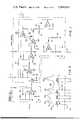
- FIGS. 1 and 2illustrate a preferred embodiment of the present invention is schematic form
- FIG. 3illustrates wave forms involved in the operation of the system of FIGS. 1 and 2.
- the output signal from a photomultiplier tube in an optical bar code readeris applied to an amplifier 20. Bars normally are printed at uniform spacing. The documents preferably are moved at uniform speed so that the frequency character of the output signal may have significance.
- the amplifierserves to convert the current output from the photomultiplier tube to a voltage. This voltage is then applied by way of an FET 21 to an amplifier 22 the operation of which is controlled through two feed back loops.
- the output of amplifier 22is connected to an input of an amplifier 23, the output of which is connected through a resistor 24 to an input of a differential amplifier 25.
- the second input of amplifier 25is supplied with a reference voltage (+5 volts) at terminal 26.
- the output of the amplifier 25is then connected by way of resistors 27 and 28 to the gate of FET 21.
- the gate-source voltage of FET 21is then varied to effectively control the gain of amplifier 22.
- a second loopis a base line loop. It is operated to maintain the lower level of the output of amplifier 22 at ground potential. This is done by connecting the output of amplifier 23 to one input of a differential amplifier 30. The second input of amplifier 30 is connected by way of resistor 31 to ground. A diode 32 is connected across amplifier 30 so that the amplifier 30 is responsive only to the negative excursions of the input voltage from amplifier 23 to produce through diode 33 a charge on capacitor 34. The charge on capacitor 34 is maintained until a new correction to the base line is to be made. The voltage across capacitor 34 is applied by way of amplifier 35 and resistor 36 to bias the input terminal of amplifier 22. It will be noted that negative bias voltage (-15 volts) is applied to amplifier 22 from terminal 37. This voltage normally maintains the output of amplifier 22 below ground potential. A positive voltage from capacitor 34 applied by way of resistor 36 serves to raise the level of the output of amplifier 22 back to ground level and maintain it at ground level.
- Bar coded signals read at a very high rateappear as a video signal to amplifier 22.
- Such signalsare illustrated by waveform 45 of FIG. 3.
- Output signals from the readervary in response to the presence and absence of bars. Peaks 45a, 45b, 45c and 45d are produced in response to sensing of bars. Signals vary with respect to the base line 45e depending upon whether or not there is a series of bar codes adjacent one another, whether there are gaps as in the zone 45f or the nature of the background of the document.
- the second loopserves to minimize changes in the base line offset. The system operates such that for a variation in amplitude of the signal over a range of 7 to 1 at the output of amplifier 20, the signal at the output of the final amplifier 40 will remain constant.
- the output of amplifier 40is then applied to the input of a nonlinear voltage divider comprising the parallel resistor diode circuit 41 and resistor 42.
- the signalis then applied to a limiter circuit comprising capacitor 43 and the oppositely polled parallel connected diodes 44.
- the limiter circuit 43, 44serves to clip the input voltage at the levels determined by the diodes 44 and causes a voltage transition at the output thereof at the instant of the change in slope of the input voltage.
- the outputis represented by the waveform 46.
- the signal represented by the waveform 46appears at the input of amplifier 50 which is a half wave rectifying amplifier.
- Amplifier 50then produces an output such as represented by the waveform 47 of FIG. 3.
- the latter signalis then applied from the output of amplifier 50, through diodes 51, 52 and 53 to the input of an active filter.
- the active filtercomprises three amplifiers 54-56 connected in tandem.
- the output of amplifier 56is connected by way of series resistors 57, 58 to the input of amplifier 54 so that the filter will ring at the bar rate to serve as a bit synchronizer.
- Line 59is connected to one input of a comparator 60.
- the second input of amplifier 60is connected to ground.
- the output of amplifier 60will be representative of any filter output voltage from line 59 above or below ground potential.
- Amplifier 60is a comparator that has a 0-5 volt output.
- the ringing signal from the active filteris squared at the output of amplifier 60, and is then applied to a shift register 61 to introduce a fixed time delay.
- the time delay involvedis a fraction of a bit time and is used to compensate for phase delay introduced in the bit synchronizer.
- a first output of the shift register 61is connected by way of line 62 to a clock input terminal of an output flip-flop 63, and through diode 64 to the dump input terminal of an integrate and dump filter which is built around a differential amplifier 65.
- the integrate and dump filteris involved in the operation of amplifier 65. It serves as a low pass filter.
- the integrator circuitincludes a capacitor 66 connected across the amplifier 65 and an input resistor 67. Capacitor 66 and resistor 67 determine the time constant of the integrator.
- the output of the integrator-dump unitis applied by way of resistor 68 to the input of a comparator involving amplifier 69 which serves as a level detector. If the voltage from resistor 68 is above a given level, then the output causes the flip-flop 70 to be set. If the signal from resistor 68 is below a given level, then the flip-flop 70 will not be set.
- the output control signalis applied from amplifier 69 to flip-flop 70 by way of an inverter 71.
- flip-flop 70is closed into flip-flop 63, then flip-flop 70 is reset by a signal from inverter 72.
- an output line 73extends from register 61 to provide a strobe signal.
- the output of flip-flop 63is connected by way of line 74 to the signal input of an output shift register 75.
- Line 73is connected to the clock input of shift register 75.
- Shift register 75thereby is provided a serial data stream fully representative of the information sensed by the photomultiplier system. Further, signal distortions caused by variations in the video background and by other noise sources are substantially reduced.
- Voltage sources B, K, J and Care isolated -15 volt sources.
- Voltage sources E, F, G and Hare isolated +15 volt sources.
- the inventionmodifies a video signal which is applied to the input to amplifier 20, and which possesses noise components in addition to signal components.
- the signalis applied to the circuit including units 22, 23, 30, 35 and 40 to produce a signal at the output of amplifier 40 having a uniform pulse height above a linear base.
- the limiter 44 and the rectifier including amplifier 50transform the stream of pulses from amplifier 40 into uniformly truncated pulses, the transitions of which are synchronous with the changes in the sign of the slope of the amplifier 40 video stream.
- the active filter circuit including amplifiers 54, 55 and 56is then caused to ring at the bit rate to synchronize the operation of the integrator involving amplifier 65 and a comparator involving amplifier 69.
- the output from the phase delay circuit of shift register 61dumps the contents of the integrator including amplifier 65 at the bit rate.
- the comparatorcauses the output flip-flops to be set depending upon whether amplitude of the integral of any of the truncated pulses applied to the integrator of circuit 65 exceeds the reference level at the time of the dump signal from the register 61.
Landscapes
- Physics & Mathematics (AREA)
- Electromagnetism (AREA)
- Engineering & Computer Science (AREA)
- Health & Medical Sciences (AREA)
- General Health & Medical Sciences (AREA)
- Toxicology (AREA)
- Artificial Intelligence (AREA)
- Computer Vision & Pattern Recognition (AREA)
- General Physics & Mathematics (AREA)
- Theoretical Computer Science (AREA)
- Facsimile Image Signal Circuits (AREA)
Abstract
Description
20, 54, 55 type 207 (National Semiconductor, Inc.) ______________________________________ amplifiers 22, 23, 30 25, 30, 40, 50, 55, 56 type 1458 (Motorola, Inc.) amplifiers 60, 69 type 311 (National Semiconductor, Inc.) amplifier inverter 71 type 74H04 (Texas Instruments, Inc.) flip-70, 63 type 7474 (Texas Instruments, Inc.) flops shift register 61 type 74163 (Texas Instruments, Inc.)resistor 27 type 3.3k ohms resistor 28 type10k ohms capacitors 19, 34 1microfarad resistor 33 3.3k ohms resistor 33a 1meg ohm resistor 36 6.8kohms resistor 37 12kohms circuit 41 1.5k ohms and1N915 diode resistor 42 820 ohms diodes 1N914capacitor 66 110picofarads resistor 67 10kohms resistor 58 12k ohms ______________________________________
Claims (12)
Priority Applications (1)
| Application Number | Priority Date | Filing Date | Title |
|---|---|---|---|
| US05/478,238US3969612A (en) | 1974-06-11 | 1974-06-11 | Bar code reader enhancement |
Applications Claiming Priority (1)
| Application Number | Priority Date | Filing Date | Title |
|---|---|---|---|
| US05/478,238US3969612A (en) | 1974-06-11 | 1974-06-11 | Bar code reader enhancement |
Publications (1)
| Publication Number | Publication Date |
|---|---|
| US3969612Atrue US3969612A (en) | 1976-07-13 |
Family
ID=23899103
Family Applications (1)
| Application Number | Title | Priority Date | Filing Date |
|---|---|---|---|
| US05/478,238Expired - LifetimeUS3969612A (en) | 1974-06-11 | 1974-06-11 | Bar code reader enhancement |
Country Status (1)
| Country | Link |
|---|---|
| US (1) | US3969612A (en) |
Cited By (11)
| Publication number | Priority date | Publication date | Assignee | Title |
|---|---|---|---|---|
| US4192452A (en)* | 1976-02-20 | 1980-03-11 | Mitsubishi Denki Kabushiki Kaisha | Information reading system |
| US4264808A (en)* | 1978-10-06 | 1981-04-28 | Ncr Corporation | Method and apparatus for electronic image processing of documents for accounting purposes |
| US4528444A (en)* | 1981-10-30 | 1985-07-09 | Nippondenso Co., Ltd. | Optical reading apparatus with automatic gain control circuit |
| US4540595A (en)* | 1982-02-01 | 1985-09-10 | International Business Machines Corporation | Article identification material and method and apparatus for using it |
| US5103080A (en)* | 1990-12-10 | 1992-04-07 | Symbol Technologies, Inc. | Digitizer signal processing circuit for a bar code |
| US5168148A (en)* | 1990-12-28 | 1992-12-01 | Symbol Technologies, Inc. | Automatic gain control circuit |
| US5380992A (en)* | 1989-07-10 | 1995-01-10 | Koninklijke Ptt Nederland B.V. | Bar code detection using background-correlated bar criterion for ascertaining the presence of a bar |
| US5410139A (en)* | 1990-08-03 | 1995-04-25 | Symbol Technologies, Inc. | Peak detecting bar code reader |
| US5461223A (en)* | 1992-10-09 | 1995-10-24 | Eastman Kodak Company | Bar code detecting circuitry |
| US8270303B2 (en) | 2007-12-21 | 2012-09-18 | Hand Held Products, Inc. | Using metadata tags in video recordings produced by portable encoded information reading terminals |
| US10942964B2 (en) | 2009-02-02 | 2021-03-09 | Hand Held Products, Inc. | Apparatus and method of embedding meta-data in a captured image |
Citations (4)
| Publication number | Priority date | Publication date | Assignee | Title |
|---|---|---|---|---|
| US3538444A (en)* | 1967-05-04 | 1970-11-03 | Mechanical Products Inc | Analog to digital signal converting system having a hysteresis creating feedback loop |
| US3631263A (en)* | 1970-01-09 | 1971-12-28 | Ibm | Signal detection circuit |
| US3654562A (en)* | 1970-07-29 | 1972-04-04 | Itt | Selectively sampling received signals |
| US3860794A (en)* | 1971-12-13 | 1975-01-14 | Bendix Corp | System for converting modulated signals to squarewave outputs |
- 1974
- 1974-06-11USUS05/478,238patent/US3969612A/ennot_activeExpired - Lifetime
Patent Citations (4)
| Publication number | Priority date | Publication date | Assignee | Title |
|---|---|---|---|---|
| US3538444A (en)* | 1967-05-04 | 1970-11-03 | Mechanical Products Inc | Analog to digital signal converting system having a hysteresis creating feedback loop |
| US3631263A (en)* | 1970-01-09 | 1971-12-28 | Ibm | Signal detection circuit |
| US3654562A (en)* | 1970-07-29 | 1972-04-04 | Itt | Selectively sampling received signals |
| US3860794A (en)* | 1971-12-13 | 1975-01-14 | Bendix Corp | System for converting modulated signals to squarewave outputs |
Cited By (14)
| Publication number | Priority date | Publication date | Assignee | Title |
|---|---|---|---|---|
| US4192452A (en)* | 1976-02-20 | 1980-03-11 | Mitsubishi Denki Kabushiki Kaisha | Information reading system |
| US4264808A (en)* | 1978-10-06 | 1981-04-28 | Ncr Corporation | Method and apparatus for electronic image processing of documents for accounting purposes |
| US4528444A (en)* | 1981-10-30 | 1985-07-09 | Nippondenso Co., Ltd. | Optical reading apparatus with automatic gain control circuit |
| US4540595A (en)* | 1982-02-01 | 1985-09-10 | International Business Machines Corporation | Article identification material and method and apparatus for using it |
| US5380992A (en)* | 1989-07-10 | 1995-01-10 | Koninklijke Ptt Nederland B.V. | Bar code detection using background-correlated bar criterion for ascertaining the presence of a bar |
| US5410139A (en)* | 1990-08-03 | 1995-04-25 | Symbol Technologies, Inc. | Peak detecting bar code reader |
| US5557094A (en)* | 1990-08-03 | 1996-09-17 | Symbol Technologies Inc | False-transition inhibitor circuit for a bar code reader |
| US5103080A (en)* | 1990-12-10 | 1992-04-07 | Symbol Technologies, Inc. | Digitizer signal processing circuit for a bar code |
| US5168148A (en)* | 1990-12-28 | 1992-12-01 | Symbol Technologies, Inc. | Automatic gain control circuit |
| US5461223A (en)* | 1992-10-09 | 1995-10-24 | Eastman Kodak Company | Bar code detecting circuitry |
| US5536929A (en)* | 1992-10-09 | 1996-07-16 | Johnson & Johnson Clinical Diagnostics, Inc. | Bar code detecting circuitry |
| US5536927A (en)* | 1992-10-09 | 1996-07-16 | Johnson & Johnson Clinical Diagnostics, Inc. | Bar code detecting circuitry |
| US8270303B2 (en) | 2007-12-21 | 2012-09-18 | Hand Held Products, Inc. | Using metadata tags in video recordings produced by portable encoded information reading terminals |
| US10942964B2 (en) | 2009-02-02 | 2021-03-09 | Hand Held Products, Inc. | Apparatus and method of embedding meta-data in a captured image |
Similar Documents
| Publication | Publication Date | Title |
|---|---|---|
| US3969612A (en) | Bar code reader enhancement | |
| US4807287A (en) | Document authentication method | |
| CA1119725A (en) | Magnetic ink character recognition waveform analyzer | |
| US4143355A (en) | Character recognition system | |
| US3000000A (en) | Automatic reading system | |
| EP0036950A1 (en) | Dynamic threshold detector | |
| DE68927148T2 (en) | Digital phase locked loop | |
| US4184179A (en) | Reproduction of binary signals from a recording medium that may be read at varying speeds | |
| US3701886A (en) | Method of representing data codes with equal width bar and device for reading same | |
| JPS63158678A (en) | Inter-word space detection method | |
| CA1037607A (en) | Retrospective pulse modulation and apparatus therefor | |
| US5274681A (en) | Clock recovery circuit with memory storage level comparison with high, medium and low thresholds | |
| EP0380601A1 (en) | Magnetic character reading apparatus. | |
| US5736722A (en) | Dual sensor decoder | |
| US4080528A (en) | Data interlacing system | |
| CA1059238A (en) | Code converter | |
| US4058706A (en) | MICR data lift system | |
| US3805175A (en) | Retrospective pulse modulation decoding method and apparatus | |
| US3641525A (en) | Self-clocking five bit record-playback system | |
| EP0464090A1 (en) | Method for modulating binary data | |
| KR870000857B1 (en) | FM code signal signal adjusting method and device | |
| JPS6230672B2 (en) | ||
| EP0344301A1 (en) | Method and apparatus for reading characters. | |
| GB1085962A (en) | System for reading and writing binary digital data on magnetic cards | |
| GB1380664A (en) | Decoder of retrospective pulse modulated information |
Legal Events
| Date | Code | Title | Description |
|---|---|---|---|
| AS | Assignment | Owner name:CHEMICAL BANK, A NY BANKING CORP. Free format text:SECURITY INTEREST;ASSIGNORS:RECOGNITION EQUIPMENT INCORPORATED;PLEXUS SOFTWARE, INC.;REEL/FRAME:005323/0509 Effective date:19891119 | |
| AS | Assignment | Owner name:RECOGNITION EQUIPMENT INCORPORATED ("REI") 2701 EA Free format text:RELEASED BY SECURED PARTY;ASSIGNOR:CHEMICAL BANK, A NY. BANKING CORP.;REEL/FRAME:005439/0823 Effective date:19900731 | |
| AS | Assignment | Owner name:FIRST NATIONAL BANK OF BOSTON, THE, AS AGENT, MASS Free format text:SECURITY INTEREST;ASSIGNORS:RECOGNITION EQUIPMENT INC.;HYBRID SYSTEMS, INC.;RECOGNITION EQUIPMENT (JAPAN), INC.;REEL/FRAME:006344/0298 Effective date:19920326 | |
| AS | Assignment | Owner name:RECOGNITION INTERNATIONAL INC., TEXAS Free format text:CHANGE OF NAME;ASSIGNOR:RECOGNITION EQUIPMENT INCORPORATED;REEL/FRAME:006462/0646 Effective date:19930312 |