US3956593A - Time space time (TST) switch with combined and distributed state store and control store - Google Patents
Time space time (TST) switch with combined and distributed state store and control storeDownload PDFInfo
- Publication number
- US3956593A US3956593AUS05/514,828US51482874AUS3956593AUS 3956593 AUS3956593 AUS 3956593AUS 51482874 AUS51482874 AUS 51482874AUS 3956593 AUS3956593 AUS 3956593A
- Authority
- US
- United States
- Prior art keywords
- switch
- time
- control
- space
- signal input
- Prior art date
- Legal status (The legal status is an assumption and is not a legal conclusion. Google has not performed a legal analysis and makes no representation as to the accuracy of the status listed.)
- Expired - Lifetime
Links
Images


Classifications
- H—ELECTRICITY
- H04—ELECTRIC COMMUNICATION TECHNIQUE
- H04Q—SELECTING
- H04Q11/00—Selecting arrangements for multiplex systems
- H04Q11/04—Selecting arrangements for multiplex systems for time-division multiplexing
- H04Q11/06—Time-space-time switching
Definitions
- This inventionrelates in general to time space time (TST) telecommunication system switches, and, in particular, to TST switches for interconnecting digital Time Division Multiplex (TDM) communication lines, using two basic modules, a plurality of time switching modules and a plurality of space switching modules.
- TSTtime space time
- TDMTime Division Multiplex
- Time Space Time (TST) switchesare a particularly useful configuration of switching elements providing both time and space translation between channels of Time Division Multiplexed (TDM) telecommunications transmission lines.
- a TST switchinterconnects digital bi-directional TDM communication lines with TDM communication involving the sharing of single transmission paths, individually, in time to provide multiple channels in a single transmission medium.
- TSTtime space time
- Another objectis to provide such a TST switch system wherein the two basic modules may be interconnected to realize virtually any size and configuration of a time division switch.
- a further objectis to achieve improved reliability and lessened maintenance requirements through use of such TST switch systems using two basic modules.
- a TST switchwith combined and distributed state and control stores
- the three circuit typesinclude the time switch module control portion, the time switch module memory portion, and the space switch module.
- the two basic modulesare interconnectable to realize virtually any size and configuration of a time division switch having distributed operation particularly with the control stores associated with the switching elements incorporated into the time switch and space switch modules.
- the space switchis integrated with the space control circuitry into a single LSI circuit. Multiple LSI circuits are configured as basic functional units providing desired flexibility in switch size and maintainability.
- the TST switch systemprovides for storage of the status of each interstage link as a distinct code in the control store associated with the output connected to each link.
- FIG. 1represents a graphic showing of a format for time division multiplexing (TDM) of digital data
- FIG. 2a combination graphic and schematic block showing of a TDM input-output time and space switch unit
- FIG. 3a block schematic showing of a basic TST switch configuration with a control source also indicated;
- FIG. 4a block schematic showing of a basic TST switch, such as shown in FIG. 3, with TDM channel content indicated for an input location and an output location;
- FIG. 5a block schematic and graphic showing of a time division space switch element
- FIG. 6a block schematic and grapic showing of a time division space switch implemented using a plurality of the space switch elements of FIG. 5;
- FIG. 7a block schematic and graphic showing of a three stage 256 ⁇ 256 time division space switch
- FIG. 8a block schematic and graphic showing of a time switch element
- FIGS. 9A and 9Bswitch inlet memory and outlet memory, respectively, timing waveforms
- FIG. 10a block schematic and graphic showing of a 16 ⁇ 16 TST switch unit such as the unit of FIG. 3, with control interconnect detail added;
- FIG. 11a block schematic and graphic showing of a 256 ⁇ 256 TST switch unit incorporating a 256 ⁇ 256 three stage time division space switch.
- TST switchesare designed to interconnect a number of digital Time Division Multiplex (TDM) communication lines with TDM involving the sharing of individual single transmission paths in time. This is with c communication channels established by dividing time into c slots.
- TDMTime Division Multiplex
- each set of c time slotsconstitutes a frame during which each communication is allowed to send a single word of b bits.
- 8-bit wordsare generated at an 8 KHz rate and, thereby, a pair of 1.536 mbps transmission links are capable of carrying 24 separate conversations.
- an 8.192 mbps linkcould accommodate 128 64 kbps channels.
- TDM inputs (1) and (15), of a plurality of input linesare shown to feed time and space switch 20 with TDM outputs (1) and (15), of a plurality of output lines emanating therefrom.
- Channel 2 of the TDM input line (1)is connected to channel 17 of the TDM output line (15), and with full duplex communication requiring a two-way circuit, a second connection path is established, as indicated by the dotted line, transferring channel 17 of TDM input line (15) to channel 2 of TDM output line (1).
- a basic TST switch configuration 21is shown in FIG. 3, with the first stage T1 of the switch being N inlet memories (actually 0 through N-1) 22(0), 22(1) . . . 22(N-1), one for each of the O through N-1 TDM inputs, respectively.
- the c channel words from each inputare stored in c successive addresses of the respective inlet memories, with these words then held in the memories until they are transferred through the space switch 23 to the outlet memories 24(0), 24(1) . . . 24(N-1) in the third stage T2, space switch 23 actually being the second stage, where the words are held in outlet memories until they are released on respective 0 through N-1 output TDM lines.
- the first stagerepresents a time switch in that data occurring in the input channels is translated in time to a time slot during which the space switch 23 transfer takes place.
- the T2 outlet memories 24(0), 24(1) . . . 24(N-1)receive data words from space switch 23 and store them in addresses corresponding to the desired output channel with the time division outputs 0 through N-1 then obtaining their data by addressing successive locations of respective outlet memories.
- a control memoryAssociated with each inlet memory, space switch stage output, and outlet memory, is a control memory that contains l words corresponding to the l time slots during which data is transferred through the space stage 23.
- the individual control storesmay be separate with individual memories, or collected together in a single control store, subject to control from control source 25 for the T1 inlet memories, the space switch 23 outputs, and the T2 outlet memories, respectively.
- This system with control source 25specifies which space switch crosspoints are selected and which inlet and outlet memory locations are accessed during each switch time slot, with the control memories being accessed in cyclic fashion so that each connection is repeated, at the same time, during every frame.
- the pathfinding operation in a TST switchinvolves a time search as well as a space search.
- the space switch connectionsare time division multiplexed with l time slots per frame, and when l is greater than c, the switch is said to be operating with time expansion. The larger l is, the more transfer opportunities there are through the space switch 23.
- greater time expansionsimply lower blocking probabilities, and for a non-blocking space switch 23, when l is increased to 2c -1 the TST blocking probability is reduced to zero.
- the control source 25sets up and takes down connections in response to requests and disconnects, acting through the control memories.
- the control source 25accesses the stored status of switching elements to determine idle switching paths and available time slots. Then, when an idle path is found, the corresponding status bits are set to "busy" and the appropriate information is loaded into the control memories. When discontinuing a connection, the control memories are accessed to determine which status bits must be set to idle.
- Master clockis distributed to all switching elements, as indicated by the plurality of arrowed leads from master clock source 26, to synchronize the operation thereof.
- the NXN space switch 23that, in FIG. 3, is a square switch with an equal number of inputs and outputs, is operated in time divided fashion in synchronism with the time stages.
- a space switchis dependent on the number of inputs and outputs it services.
- a single stage square space switchsuch as the NXN space switch 23 of FIG. 3, is generally most attractive for small switches. Large switches, however, are more attractively implemented with multiple stages.
- the TST switch 27shows a space switch 28 transfer made, such as shown in FIG. 2, for a connection between channel 2 of line 1 and channel 17 of line 15.
- switching time slot 22has been selected for the transfer from inlet 1 to outlet 15.
- the T1 inlet memories 29(1), 29(2), . . . 29(15)are like the T1 memories 22 of FIG. 3, and the T 2 outlet memories 30(1), 30(2), . . . 30(15) are like the T2 memories 24 of FIG. 3.
- the various elements of TST switch 27are controlled by cyclicly retrieving control information from a set of memories, just as with the embodiment of FIG. 3.
- New connectionsare set up and existing connections taken down by updating the information stored in the control memories, one of which is associatied with each inlet memory, space stage output, and outlet memory.
- the control memoriescontain one word for each time slot, with the information stored in the words specifying which connections are established during the respective time slots.
- control storescan be implemented using ramdom access memories and a counter to effect cyclic retrieval. The counter would operate in a modulo L (144) fashion. Thus, addresses 0 through 143 would be accessed sequentially with word 0 being addressed after word 143.
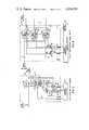
- the time division switch element circuit 31 of FIG. 5includes a switching mechanism with a 16 to 1 selector 32 controlled by the output of a 144 ⁇ 5 end around shift register 33 to selectively connect one of 0 through 15 TDM inputs to the single TDM output line 34.
- the 144 ⁇ 5 end around shift register circuit 33 constituting a control storehas a five-line output 35 connected to the 16 to 1 selector 32, and also through recirculation loop 36 to gates 37 and 38, and through gate 37 to the bottom of the shift register 33.
- the recirculation loop 36is also connected through gate 38 to a control data link 39 interconnecting control circuitry 40 and an additional gate 41.
- Gate 41has an output line link 42 connection to line link 43 interconnecting gate 37 and the bottom of shift register 33.
- Read signalsare fed from control circuitry 40 through read line 44 to control gate 38.
- Write signalsare fed from control circuitry 40 through write line 45 directly to gate 41 and also through inverter amplifier 46 to gate 37 for control of both gates 37 and 41.
- Clock line 47feeds time slot clock from control circuitry 40 to the end around shift register circuit 33.
- This same procedureis also used to take down a connection by writing an idle code into the appropriate time slot.
- the control word in current usecan be gated onto the control data bus 39 through gate 38 by setting the READ input to a " ONE".
- connectionscan be traced and status of a particular element determined.
- the implementation of FIG. 5uses 4 bits of a control word to specify one of 16 connections and 1 bit to designate busy/idle status of the respective time slot. If an idle output is designated by a distinct 5-bit code, one of 31 inputs could be selected by the remaining codes, alternately, a 4-bit control word can control 15 inputs and leave a distinct code to designate an idle output.
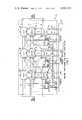
- FIG. 6A complete switching array implemented through interconnecting a plurality of the time division switch element circuits 31 of FIG. 5 is shown in FIG. 6 as a 16 ⁇ 16 time division space switch 48. Sixteen 16 ⁇ 1 element circuits 31 are used, with each 16 to 1 matrix selector 32 input connected to a corresponding input of every element, and the sixteen distinct outputs 0 through 15 are individually controlled by their respective control stores.
- READ line 44' from control circuitry 40'is fanned out selectively to sixteen READ lines 44 for individual switch element circuits 31 through the switching mechanism of 1 to 16 selector 49
- WRITE line 45' from control circuitry 40'is fanned out selectively to sixteen WRITE lines 45 for individual switch element circuits 31 through the switching mechanism of 1 to 16 selector 50.
- the 1 to 16 selectors 49 and 50are controlled by control inputs from control circuitry 40' passed through control address bus 51 to the selectors 49 and 50.
- Time slot clock 47is connected from control circuitry 40' to the switch element circuits 31.
- sixteen of the 16 ⁇ 16 time division space switches 48are used in each of the three stages, forty-eight in all. Sixteen TDM inputs are fed individually to each of the space switches 48 in the first stage S 1 , thereby providing for 256 data inputs to the time divided space switch 52. Sixteen outputs of each first stage S 1 space switch 48 are individually cross-connected to inputs of space switches 48 of the second stage S 2 that are, in like manner, cross-connected to inputs of space switches 48 of the third stage S 3 , from each of which sixteen TDM outputs are provided to total 256 data outputs, in all, from space switch 52.
- READ line 44" from control circuitry 40"is fanned out selectively to sixteen READ lines 44' for individual space switches 48 of a switch stage through the switching mechanism of 1 to 16 selectors 49', in parallel, for the three stages S 1 , S 2 , and S 3 .
- WRITE line 45" from control circuitry 40”is fanned out selectively to sixteen WRITE lines 45', for individual space switches 48 of a switch stage through the switching mechanism of 1 to 16 selectors 50', in parallel, for the three stages S 1 , S 2 , and S 3 .
- the 1 to 16 selectors 49' and 50'are controlled by address inputs from control circuitry 40", passed through control address buses 53, one for each of the three stages S 1 , S 2 , and S 3 , to the selectors 49' and 50'.
- control circuitry 40passed through control address buses 53, one for each of the three stages S 1 , S 2 , and S 3 , to the selectors 49' and 50'.
- the number of individual lines in respective busessuch as 39 and 36 in FIG. 5, and 39' and 51 and FIG. 6, and elsewhere, are indicated by a number at a slant line through each respective bus.
- a three-stage 256 ⁇ 256 time division space switchis provided with each stage consisting of sixteen 16 ⁇ 16 switching matrices with the entire switch requiring 768 individual 16 ⁇ 1 space switch elements 31. Individual elements are addressed to set up or take down connections by loading the appropriate information on the control store data and address buses, and with separate buses being used as set forth for each stage, the stages are addressable simultaneously thereby allowing a complete path to be set up or taken down in one operation.
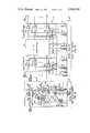
- the time switch element 54includes a data memory 55 with the data input fed through a series to parallel shift register conversion unit 56.
- the data outputis fed through parallel to series shift register conversion unit 57 as stepped along with unit 56 by bit clock applied through line 58 from control circuitry 40'".
- the data memory 55 addressesare obtained from the seven line output 59 of 144 ⁇ 7 end around shift register 60, as passed by gate 61 and seven line bus 62, or by the seven line output 63 of counter 64, as passed by gate 65 and bus 62.
- Read/write (R/W) controlis obtained through line 66 form control circuitry 40'".
- the 144 ⁇ 7 end around shift register circuit 60 constituting a control storehas the seven line output 59 also connected through recirculation loop 67 to gates 68 and 69, and through gate 68 to the bottom of the shift register 60.
- the recirculation loop 67is also connected through gate 69 to a control data link 70 interconnecting control circuitry 40'" and an additional gate 71.
- Gate 71is output joined together with gate 68 via bus system 72 as the seven line input to the bottom of shift register 60.
- Read signalsare fed from control circuitry 40'" through read line 73 to control gate 69.
- Write signalsare fed from control circuitry 40'" through write line 74 directly to gate 71 and also through inverter amplifier 75 to gate 68 for control of both gates 68 and 71.
- data memory 55 address selection signalsare fed from control circuitry 40'" through CTR/CS line 76 directly to counter gate 65 and also through inverter amplifier 77 to gate 61 for control of both gates 61 and 65, with only one gate being open, at a time, for signal flow.
- memory addressesare obtained from either of two sources; from counter 64, when CTR/CS is "ONE", or from the control store shift register when CTR/CS is "ZERO".
- Bit clock line 58feeds bit clock from control circuitry 40'" to the series to parallel (S/P) conversion unit 56, and to the parallel to series (P/S) conversion unit 57.
- Reset signals from control circuitry 40'"are fed to counter 64 through reset line 78, with reset being used to initialize the counter circuit when power is first applied in a power on, clear, action.
- the time switch element circuit 54 of FIG. 8is usable as either an output oriented time switch or as an input oriented time switch.
- incoming datais stored in sequential memory locations, but random access is employed for output data.
- memory addressesare obtained by selecting counter outputs during data memory writes, and the control store outputs are obtained during data memory reads.
- Output oriented time switchesare used as inlet memory stages with the TST switches set forth herein. Input oriented time switches, conversely, write randomly, but read sequentially, with the counter output selected during data memory reads and the control store output selected during data memory writes.
- input oriented time switchesare used as outlet memory stages with the TST switches of this case.
- FIGS. 9A and 9Bare waveforms for the basic time switch element circuit 54 used in the two modes of operation. This difference in operation is determined merely by the sense of the CTR/CS input with respect to the R/W input.
- the CTR/CS inputis inverted with respect to the R/W waveform, while for inlet memory use, the CTR/CS is the same as, and can be obtained driectly from, the R/W source.
- the R/W inputserves not only to control the data memory operation, but serves also to increment the counter and to shift control words in the control store.
- the control storeoperates as a recirculating shift register. However, whenever the "WRITE" input is active, the recirculation is blocked by gate 68, and new data is inserted into the control store by passing data from control bus 70 through gate 71 to the shift register 60.
- a data memory with 128 wordsrequires 7 bits of address.
- the control storeis 7 bits wide, with 144 words, for a switch with 144 internal time slots.
- An idle time slotis encoded as one particular 7-bit code. Thus, only 127 memory locations are actually available for message data.
- a time expansion of 144/1281.125 is realized by operating the memory R/W cycle at 868 ns. intervals. As 144 opportunities exist to write into an inlet memory, 16 inlet memory write accesses are unused. Similarly, 16 outlet memory read accesses are unused.
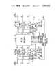
- Time switching stages of a TST switchare implemented using a plurality of time switch elements 54 such as shown in the 16 ⁇ 16 TST switch 79 of FIG. 10 with 16 time switch elements used of the T 1 inlet stage 80, and 16 time switch elements used for the T 2 outlet stage 81.
- the 16 ⁇ 16 space switch 48is implemented using 16 of the space switch elements 31 of FIG. 5, as shown in FIG. 6.
- the 1 ⁇ 16 selector read and write circuits 82 and 83operated by control addresses through four line buses 84 from control circuitry 40'", are used to address individual switch elements when reading from or writing into the selected control stores.
- Control circuitry 40'"is the initiating source for the necessary control signals and feeds the address and data buses to set up and take down connections.
- T 1 and T 2 stage control datais fed through seven line buses 70' that branch into buses 70 for the respective time switch elements 54.
- the T 1 and T 2 stage address buses 84control the 1 ⁇ 16 selector circuits 82 and 83, to distribute read and write control signals from control circuitry 40'" passed through read line 73' and write line 74' to the plurality of read lines 73 and the plurality of write lines 74 in both the T 1 inlet stage 80 and T 2 outlet stage 81.
- the 256 ⁇ 256 TST switch 85 of FIG. 11is much like the TST switch 79 of FIG. 10; the major difference being that of capacity, in having sixteen times the line capability of TST switch 79.
- the 256 ⁇ 256 3-stage time divided space switch 52 of the TST switch 79is the same as that of FIG. 7, indicated in greatly simplified, single block form, with some control inputs and outputs interconnected to the expanded control circuitry 40"E.
- the T 1 and T 2 data buses 70"connect to a plurality of sixteen time switch element 54 unit sections 80 and 81 in the memory stages.
- the T 1 and T 2 address buses 84'are shown as 8-line buses extending from control circuitry 40"E, splitting into two 4-line bus branches; branch 84, connected to selectors 82 and 83, with each of the plurality of unit sections 80 and 81, and a branch 84S extended to 1 ⁇ 116 read selectors 86 and 1 ⁇ 16 write selectors 87 that are connected to read line 44" and write line 45", respectively, for addressing control to unit sections 80 and 81.
- a higher capacity TST switchis implemented, using 256 time switch elements in the inlet stage T 1 , 256 time switch elements in the outlet stage T 2 , and 256 space switch elements in each of three space stages S 1 , S 2 , and S 3 .
- control circuitry 40"Egenerates the necessary control signals and operates to feed address and data buses to set up or take down connections.
Landscapes
- Engineering & Computer Science (AREA)
- Computer Networks & Wireless Communication (AREA)
- Use Of Switch Circuits For Exchanges And Methods Of Control Of Multiplex Exchanges (AREA)
Abstract
Description
Claims (33)
Priority Applications (1)
| Application Number | Priority Date | Filing Date | Title |
|---|---|---|---|
| US05514828US3956593B2 (en) | 1974-10-15 | 1974-10-15 | Time space time(tst)switch with combined and distributed state store and control store |
Applications Claiming Priority (1)
| Application Number | Priority Date | Filing Date | Title |
|---|---|---|---|
| US05514828US3956593B2 (en) | 1974-10-15 | 1974-10-15 | Time space time(tst)switch with combined and distributed state store and control store |
Publications (3)
| Publication Number | Publication Date |
|---|---|
| US3956593Atrue US3956593A (en) | 1976-05-11 |
| US3956593B1 US3956593B1 (en) | 1990-04-17 |
| US3956593B2 US3956593B2 (en) | 1993-05-25 |
Family
ID=24048858
Family Applications (1)
| Application Number | Title | Priority Date | Filing Date |
|---|---|---|---|
| US05514828Expired - LifetimeUS3956593B2 (en) | 1974-10-15 | 1974-10-15 | Time space time(tst)switch with combined and distributed state store and control store |
Country Status (1)
| Country | Link |
|---|---|
| US (1) | US3956593B2 (en) |
Cited By (42)
| Publication number | Priority date | Publication date | Assignee | Title |
|---|---|---|---|---|
| US4032719A (en)* | 1975-06-26 | 1977-06-28 | International Business Machines Corporation | Modular slot interchange digital exchange |
| US4064360A (en)* | 1976-07-06 | 1977-12-20 | The United States Of America As Represented By The Secretary Of The Navy | High speed digital switch |
| US4075608A (en)* | 1976-01-19 | 1978-02-21 | The United States Of America As Represented By The Secretary Of The Navy | Multiple-channel data switch |
| US4081611A (en)* | 1975-04-14 | 1978-03-28 | Societa Italiana Telecomunicazioni Siemens S.P.A. | Coupling network for time-division telecommunication system |
| US4092497A (en)* | 1976-01-20 | 1978-05-30 | Jeumont-Schneider | Connection network for PCM TDM automatic telephone exchange equipment |
| US4093827A (en)* | 1976-02-17 | 1978-06-06 | Thomson-Csf | Symmetrical time division matrix and a network equipped with this kind of matrix |
| FR2371845A1 (en)* | 1976-11-20 | 1978-06-16 | Int Standard Electric Corp | MULTI-STAGE SWITCHING NETWORK FOR TIME-DIVIDED MULTIPLEXING |
| US4097693A (en)* | 1975-06-16 | 1978-06-27 | U.S. Philips Corporation | Switching system for an automatic telecommunication exchange with a plurality of intermediate lines that are grounded when not in use |
| US4101737A (en)* | 1975-06-26 | 1978-07-18 | Plessey Handel Und Investments Ag | Control arrangement in a time-space-time (t-s-t) time division multiple (t.d.m.) telecommunication switching system |
| FR2390878A1 (en)* | 1977-05-12 | 1978-12-08 | Ibm | MODULAR SWITCHING SYSTEM |
| FR2408267A1 (en)* | 1977-11-07 | 1979-06-01 | Post Office | IMPROVEMENTS TO DIGITAL SIGNAL SWITCHING DEVICES |
| US4186277A (en)* | 1976-01-23 | 1980-01-29 | Siemens Aktiengesellschaft | Time division multiplex telecommunications switching network |
| WO1980000289A1 (en)* | 1978-07-21 | 1980-02-21 | Stromberg Carlson Corp | Selectively controlled digital pad |
| DE2942235A1 (en)* | 1978-10-19 | 1980-04-30 | Nippon Telegraph & Telephone | TIME MULTIPLEX CIRCUIT |
| US4218588A (en)* | 1977-09-30 | 1980-08-19 | Le Materiel Telephonique | Digital signal switching system |
| US4254498A (en)* | 1978-02-01 | 1981-03-03 | Nippon Telegraph And Telephone Public Corporation | Time division telephone switching systems |
| US4268722A (en)* | 1978-02-13 | 1981-05-19 | Motorola, Inc. | Radiotelephone communications system |
| US4298977A (en)* | 1979-09-10 | 1981-11-03 | Bell Telephone Laboratories, Incorporated | Broadcast and alternate message time slot interchanger |
| US4322843A (en)* | 1979-12-26 | 1982-03-30 | Bell Telephone Laboratories, Incorporated | Control information communication arrangement for a time division switching system |
| FR2507372A1 (en)* | 1981-06-09 | 1982-12-10 | Nippon Telegraph & Telephone | MEMORY DEVICE OF THE SEQUENTIAL AND SELECTIVE WRITE-READ TYPE FROM ADDRESS INFORMATION |
| US4392223A (en)* | 1980-12-23 | 1983-07-05 | Gte Automatic Electric Laboratories, Inc. | Dual rail time and control unit for a T-S-T-digital switching system |
| US4399533A (en)* | 1980-12-23 | 1983-08-16 | Gte Automatic Electric Labs Inc. | Dual rail time and control unit for a T-S-T-digital switching system |
| US4399534A (en)* | 1980-12-23 | 1983-08-16 | Gte Automatic Electric Labs Inc. | Dual rail time and control unit for a duplex T-S-T-digital switching system |
| US4399369A (en)* | 1980-12-23 | 1983-08-16 | Gte Automatic Electric Labs Inc. | Dual rail time and control unit for a duplex T-S-T-digital switching system |
| EP0086634A1 (en)* | 1982-02-10 | 1983-08-24 | Nippon Telegraph And Telephone Corporation | Memory circuitry for use in a digital time division switching system |
| US4402077A (en)* | 1980-12-23 | 1983-08-30 | Gte Automatic Electric Labs Inc. | Dual rail time and control unit for a duplex T-S-T-digital switching system |
| US4406005A (en)* | 1980-12-23 | 1983-09-20 | Gte Automatic Electric Labs Inc. | Dual rail time control unit for a T-S-T-digital switching system |
| US4524442A (en)* | 1983-06-22 | 1985-06-18 | Gte Automatic Electric Inc. | Modularly expandable space stage for a T-S-T digital switching system |
| US4564937A (en)* | 1983-12-22 | 1986-01-14 | Gte Automatic Electric Incorporated | Remote data link address sequencer and a memory arrangement for accessing and storing digital data |
| US4701907A (en)* | 1986-02-03 | 1987-10-20 | Arthur A. Collins, Inc. | Dynamically reconfigurable time-space-time digital switch and network |
| USRE32900E (en)* | 1983-12-06 | 1989-04-04 | American Telephone And Telegraph Company, At&T Bell Laboratories | Fast circuit switching system |
| US4905219A (en)* | 1983-09-22 | 1990-02-27 | Aetna Life Insurance Company | Three level distributed control for networking I/O devices |
| US5016247A (en)* | 1989-08-07 | 1991-05-14 | Ibm Corporation | Multihop time assigned speech interpolation (TASI) system for telecommunication networks |
| US5115428A (en)* | 1989-09-05 | 1992-05-19 | The University Of Colorado Foundation, Inc. | Serial array time-slot interchangers |
| US5381406A (en)* | 1991-08-30 | 1995-01-10 | Nec Corporation | Time switching circuit |
| US5430716A (en)* | 1993-01-15 | 1995-07-04 | At&T Corp. | Path hunt for efficient broadcast and multicast connections in multi-stage switching fabrics |
| US5434857A (en)* | 1993-08-25 | 1995-07-18 | Fujitsu Limited | Circuit for confirming a connection route of address control memory |
| US20020091865A1 (en)* | 1997-06-27 | 2002-07-11 | Sun Microsystems, Inc. | Electro-optically connected multiprocessor configuration |
| US20030021267A1 (en)* | 2001-07-12 | 2003-01-30 | Velio Communications, Inc. | Non-blocking grooming switch |
| US6590900B1 (en) | 1998-12-16 | 2003-07-08 | Pmc-Sierra Ltd. | Time and space sliced non-blocking network switching fabric |
| US20040062228A1 (en)* | 2002-09-27 | 2004-04-01 | Velio Communications, Inc. | Digital cross-connect |
| US7680033B1 (en)* | 2003-10-20 | 2010-03-16 | Ciena Corporation | Network manager circuit rediscovery and repair |
Citations (3)
| Publication number | Priority date | Publication date | Assignee | Title |
|---|---|---|---|---|
| US3715505A (en)* | 1971-03-29 | 1973-02-06 | Bell Telephone Labor Inc | Time-division switch providing time and space switching |
| US3740480A (en)* | 1971-12-27 | 1973-06-19 | Bell Telephone Labor Inc | Time division multiplex switching system utilizing all time division techniques |
| US3796835A (en)* | 1970-09-30 | 1974-03-12 | Ibm | Switching system for tdm data which induces an asynchronous submultiplex channel |
- 1974
- 1974-10-15USUS05514828patent/US3956593B2/ennot_activeExpired - Lifetime
Patent Citations (3)
| Publication number | Priority date | Publication date | Assignee | Title |
|---|---|---|---|---|
| US3796835A (en)* | 1970-09-30 | 1974-03-12 | Ibm | Switching system for tdm data which induces an asynchronous submultiplex channel |
| US3715505A (en)* | 1971-03-29 | 1973-02-06 | Bell Telephone Labor Inc | Time-division switch providing time and space switching |
| US3740480A (en)* | 1971-12-27 | 1973-06-19 | Bell Telephone Labor Inc | Time division multiplex switching system utilizing all time division techniques |
Cited By (52)
| Publication number | Priority date | Publication date | Assignee | Title |
|---|---|---|---|---|
| US4081611A (en)* | 1975-04-14 | 1978-03-28 | Societa Italiana Telecomunicazioni Siemens S.P.A. | Coupling network for time-division telecommunication system |
| US4097693A (en)* | 1975-06-16 | 1978-06-27 | U.S. Philips Corporation | Switching system for an automatic telecommunication exchange with a plurality of intermediate lines that are grounded when not in use |
| US4101737A (en)* | 1975-06-26 | 1978-07-18 | Plessey Handel Und Investments Ag | Control arrangement in a time-space-time (t-s-t) time division multiple (t.d.m.) telecommunication switching system |
| US4032719A (en)* | 1975-06-26 | 1977-06-28 | International Business Machines Corporation | Modular slot interchange digital exchange |
| US4075608A (en)* | 1976-01-19 | 1978-02-21 | The United States Of America As Represented By The Secretary Of The Navy | Multiple-channel data switch |
| US4092497A (en)* | 1976-01-20 | 1978-05-30 | Jeumont-Schneider | Connection network for PCM TDM automatic telephone exchange equipment |
| US4186277A (en)* | 1976-01-23 | 1980-01-29 | Siemens Aktiengesellschaft | Time division multiplex telecommunications switching network |
| US4093827A (en)* | 1976-02-17 | 1978-06-06 | Thomson-Csf | Symmetrical time division matrix and a network equipped with this kind of matrix |
| US4064360A (en)* | 1976-07-06 | 1977-12-20 | The United States Of America As Represented By The Secretary Of The Navy | High speed digital switch |
| FR2371845A1 (en)* | 1976-11-20 | 1978-06-16 | Int Standard Electric Corp | MULTI-STAGE SWITCHING NETWORK FOR TIME-DIVIDED MULTIPLEXING |
| FR2390878A1 (en)* | 1977-05-12 | 1978-12-08 | Ibm | MODULAR SWITCHING SYSTEM |
| US4218588A (en)* | 1977-09-30 | 1980-08-19 | Le Materiel Telephonique | Digital signal switching system |
| FR2408267A1 (en)* | 1977-11-07 | 1979-06-01 | Post Office | IMPROVEMENTS TO DIGITAL SIGNAL SWITCHING DEVICES |
| FR2408265A1 (en)* | 1977-11-07 | 1979-06-01 | Post Office | TELEPHONE SWITCHING DEVICE |
| FR2408266A1 (en)* | 1977-11-07 | 1979-06-01 | Post Office | SWITCHING DEVICE FOR DIGITAL SIGNALS |
| US4306303A (en)* | 1977-11-07 | 1981-12-15 | The Post Office | Switching of digital signals |
| US4254498A (en)* | 1978-02-01 | 1981-03-03 | Nippon Telegraph And Telephone Public Corporation | Time division telephone switching systems |
| US4268722A (en)* | 1978-02-13 | 1981-05-19 | Motorola, Inc. | Radiotelephone communications system |
| WO1980000289A1 (en)* | 1978-07-21 | 1980-02-21 | Stromberg Carlson Corp | Selectively controlled digital pad |
| US4220823A (en)* | 1978-07-21 | 1980-09-02 | Stromberg-Carlson Corporation | Selectively controlled digital pad |
| DE2942235A1 (en)* | 1978-10-19 | 1980-04-30 | Nippon Telegraph & Telephone | TIME MULTIPLEX CIRCUIT |
| US4298977A (en)* | 1979-09-10 | 1981-11-03 | Bell Telephone Laboratories, Incorporated | Broadcast and alternate message time slot interchanger |
| US4322843A (en)* | 1979-12-26 | 1982-03-30 | Bell Telephone Laboratories, Incorporated | Control information communication arrangement for a time division switching system |
| US4399534A (en)* | 1980-12-23 | 1983-08-16 | Gte Automatic Electric Labs Inc. | Dual rail time and control unit for a duplex T-S-T-digital switching system |
| US4406005A (en)* | 1980-12-23 | 1983-09-20 | Gte Automatic Electric Labs Inc. | Dual rail time control unit for a T-S-T-digital switching system |
| US4399533A (en)* | 1980-12-23 | 1983-08-16 | Gte Automatic Electric Labs Inc. | Dual rail time and control unit for a T-S-T-digital switching system |
| US4392223A (en)* | 1980-12-23 | 1983-07-05 | Gte Automatic Electric Laboratories, Inc. | Dual rail time and control unit for a T-S-T-digital switching system |
| US4399369A (en)* | 1980-12-23 | 1983-08-16 | Gte Automatic Electric Labs Inc. | Dual rail time and control unit for a duplex T-S-T-digital switching system |
| US4402077A (en)* | 1980-12-23 | 1983-08-30 | Gte Automatic Electric Labs Inc. | Dual rail time and control unit for a duplex T-S-T-digital switching system |
| FR2507372A1 (en)* | 1981-06-09 | 1982-12-10 | Nippon Telegraph & Telephone | MEMORY DEVICE OF THE SEQUENTIAL AND SELECTIVE WRITE-READ TYPE FROM ADDRESS INFORMATION |
| EP0086634A1 (en)* | 1982-02-10 | 1983-08-24 | Nippon Telegraph And Telephone Corporation | Memory circuitry for use in a digital time division switching system |
| US4512012A (en)* | 1982-02-10 | 1985-04-16 | Fujitsu Limited | Time-switch circuit |
| US4524442A (en)* | 1983-06-22 | 1985-06-18 | Gte Automatic Electric Inc. | Modularly expandable space stage for a T-S-T digital switching system |
| US4905219A (en)* | 1983-09-22 | 1990-02-27 | Aetna Life Insurance Company | Three level distributed control for networking I/O devices |
| USRE32900E (en)* | 1983-12-06 | 1989-04-04 | American Telephone And Telegraph Company, At&T Bell Laboratories | Fast circuit switching system |
| US4564937A (en)* | 1983-12-22 | 1986-01-14 | Gte Automatic Electric Incorporated | Remote data link address sequencer and a memory arrangement for accessing and storing digital data |
| US4701907A (en)* | 1986-02-03 | 1987-10-20 | Arthur A. Collins, Inc. | Dynamically reconfigurable time-space-time digital switch and network |
| US4797589A (en)* | 1986-02-03 | 1989-01-10 | Arthur A. Collins, Inc. | Dynamically reconfigurable time-space-time digital switch and network |
| US5016247A (en)* | 1989-08-07 | 1991-05-14 | Ibm Corporation | Multihop time assigned speech interpolation (TASI) system for telecommunication networks |
| US5115428A (en)* | 1989-09-05 | 1992-05-19 | The University Of Colorado Foundation, Inc. | Serial array time-slot interchangers |
| WO1991004642A3 (en)* | 1989-09-05 | 1992-11-26 | Univ Colorado Foundation | Serial array time-slot interchangers |
| US5381406A (en)* | 1991-08-30 | 1995-01-10 | Nec Corporation | Time switching circuit |
| US5430716A (en)* | 1993-01-15 | 1995-07-04 | At&T Corp. | Path hunt for efficient broadcast and multicast connections in multi-stage switching fabrics |
| US5434857A (en)* | 1993-08-25 | 1995-07-18 | Fujitsu Limited | Circuit for confirming a connection route of address control memory |
| US6859844B2 (en)* | 1997-06-27 | 2005-02-22 | Sun Microsystems, Inc. | Electro-optically connected multiprocessor configuration including a ring structured shift-register |
| US20020091865A1 (en)* | 1997-06-27 | 2002-07-11 | Sun Microsystems, Inc. | Electro-optically connected multiprocessor configuration |
| US6590900B1 (en) | 1998-12-16 | 2003-07-08 | Pmc-Sierra Ltd. | Time and space sliced non-blocking network switching fabric |
| US20030021267A1 (en)* | 2001-07-12 | 2003-01-30 | Velio Communications, Inc. | Non-blocking grooming switch |
| US7154887B2 (en) | 2001-07-12 | 2006-12-26 | Lsi Logic Corporation | Non-blocking grooming switch |
| US20040062228A1 (en)* | 2002-09-27 | 2004-04-01 | Velio Communications, Inc. | Digital cross-connect |
| US7349387B2 (en) | 2002-09-27 | 2008-03-25 | Wu Ephrem C | Digital cross-connect |
| US7680033B1 (en)* | 2003-10-20 | 2010-03-16 | Ciena Corporation | Network manager circuit rediscovery and repair |
Also Published As
| Publication number | Publication date |
|---|---|
| US3956593B2 (en) | 1993-05-25 |
| US3956593B1 (en) | 1990-04-17 |
Similar Documents
| Publication | Publication Date | Title |
|---|---|---|
| US3956593A (en) | Time space time (TST) switch with combined and distributed state store and control store | |
| US4005272A (en) | Time folded TST (time space time) switch | |
| US4173713A (en) | Continuously expandable switching network | |
| US4038497A (en) | Hardwired marker for time folded tst switch with distributed control logic and automatic path finding, set up and release | |
| US4771420A (en) | Time slot interchange digital switched matrix | |
| US4123624A (en) | Switching network for a PCM TDM system | |
| US3927267A (en) | Time division switching system of the {37 time-space-time{38 {0 type | |
| US5014268A (en) | Parallel time slot interchanger matrix and switch block module for use therewith | |
| US3851105A (en) | Time division switching network employing space division stages | |
| US4293946A (en) | Trilateral duplex path conferencing system with broadcast capability | |
| EP0039948B1 (en) | Pcm switching element | |
| US4272844A (en) | Multiplex time division switching network unit of the time-time type | |
| US4873682A (en) | Digital key telephone system | |
| US4025725A (en) | Telecommunication switching network having a multistage reversed trunking scheme and switching on a four wire basis | |
| US3991276A (en) | Time-space-time division switching network | |
| US3705266A (en) | Telephone switching systems | |
| US4494229A (en) | Interconnecting apparatus for a distributed switching telephone system | |
| GB1398519A (en) | Time division multiplex telecommunications systems | |
| US3881064A (en) | Pulse code modulation time division switching system | |
| US5042030A (en) | Apparatus for rearranging signal channels of a multi-loop time-division multiplexed transmission system | |
| US3812294A (en) | Bilateral time division multiplex switching system | |
| GB1470701A (en) | Digital switching system | |
| US3632884A (en) | Time division communication system | |
| GB1560192A (en) | Continuously expandable switching network | |
| US4186277A (en) | Time division multiplex telecommunications switching network |
Legal Events
| Date | Code | Title | Description |
|---|---|---|---|
| STCF | Information on status: patent grant | Free format text:PATENTED FILE - (OLD CASE ADDED FOR FILE TRACKING PURPOSES) | |
| AS | Assignment | Owner name:ARTHUR A. COLLINS INC., P.O. BOX 792308, 13616 NEU Free format text:ASSIGNMENT OF ASSIGNORS INTEREST.;ASSIGNOR:ARTHUR A. COLLINS, INC., 13601 PRESTON ROAD, SUITE 509W DALLAS, TX., 75240;REEL/FRAME:004450/0188 | |
| AS | Assignment | Owner name:SEVIN ROSEN BAYLESS BOROVOY, 2 GALLERIA TOWER, 134 Free format text:ASSIGNMENT OF ASSIGNORS INTEREST.;ASSIGNOR:ARTHUR A COLLINS INC.;REEL/FRAME:004688/0114 Effective date:19860414 Owner name:SEVIN ROSEN BAYLESS BOROVOY,TEXAS Free format text:ASSIGNMENT OF ASSIGNORS INTEREST;ASSIGNOR:ARTHUR A COLLINS INC.;REEL/FRAME:004688/0114 Effective date:19860414 | |
| RR | Request for reexamination filed | Effective date:19890621 | |
| B1 | Reexamination certificate first reexamination | ||
| AS | Assignment | Owner name:COLLINS LICENSING L.P. A TX LIMITED PARTNERSHIP, Free format text:ASSIGNMENT OF ASSIGNORS INTEREST.;ASSIGNOR:SEVIN ROSEN BAYLESS BOROVOY, A LIMITED PARTNERSHIP OF TX;REEL/FRAME:005719/0600 Effective date:19901201 | |
| RR | Request for reexamination filed | Effective date:19910604 | |
| RR | Request for reexamination filed | Effective date:19910604 | |
| RR | Request for reexamination filed | Effective date:19911217 | |
| RR | Request for reexamination filed | Effective date:19920715 |