US3631298A - Woven interconnection structure - Google Patents
Woven interconnection structureDownload PDFInfo
- Publication number
- US3631298A US3631298AUS869029AUS3631298DAUS3631298AUS 3631298 AUS3631298 AUS 3631298AUS 869029 AUS869029 AUS 869029AUS 3631298D AUS3631298D AUS 3631298DAUS 3631298 AUS3631298 AUS 3631298A
- Authority
- US
- United States
- Prior art keywords
- filaments
- circuit
- terminals
- fabric
- woven
- Prior art date
- Legal status (The legal status is an assumption and is not a legal conclusion. Google has not performed a legal analysis and makes no representation as to the accuracy of the status listed.)
- Expired - Lifetime
Links
Images


Classifications
- D—TEXTILES; PAPER
- D03—WEAVING
- D03D—WOVEN FABRICS; METHODS OF WEAVING; LOOMS
- D03D11/00—Double or multi-ply fabrics not otherwise provided for
- D—TEXTILES; PAPER
- D03—WEAVING
- D03D—WOVEN FABRICS; METHODS OF WEAVING; LOOMS
- D03D1/00—Woven fabrics designed to make specified articles
- D03D1/0088—Fabrics having an electronic function
- H—ELECTRICITY
- H05—ELECTRIC TECHNIQUES NOT OTHERWISE PROVIDED FOR
- H05K—PRINTED CIRCUITS; CASINGS OR CONSTRUCTIONAL DETAILS OF ELECTRIC APPARATUS; MANUFACTURE OF ASSEMBLAGES OF ELECTRICAL COMPONENTS
- H05K1/00—Printed circuits
- H05K1/02—Details
- H05K1/0277—Bendability or stretchability details
- H05K1/0283—Stretchable printed circuits
- H—ELECTRICITY
- H05—ELECTRIC TECHNIQUES NOT OTHERWISE PROVIDED FOR
- H05K—PRINTED CIRCUITS; CASINGS OR CONSTRUCTIONAL DETAILS OF ELECTRIC APPARATUS; MANUFACTURE OF ASSEMBLAGES OF ELECTRICAL COMPONENTS
- H05K1/00—Printed circuits
- H05K1/02—Details
- H05K1/03—Use of materials for the substrate
- H05K1/038—Textiles
- H—ELECTRICITY
- H05—ELECTRIC TECHNIQUES NOT OTHERWISE PROVIDED FOR
- H05K—PRINTED CIRCUITS; CASINGS OR CONSTRUCTIONAL DETAILS OF ELECTRIC APPARATUS; MANUFACTURE OF ASSEMBLAGES OF ELECTRICAL COMPONENTS
- H05K1/00—Printed circuits
- H05K1/18—Printed circuits structurally associated with non-printed electric components
- H05K1/189—Printed circuits structurally associated with non-printed electric components characterised by the use of a flexible or folded printed circuit
- H—ELECTRICITY
- H05—ELECTRIC TECHNIQUES NOT OTHERWISE PROVIDED FOR
- H05K—PRINTED CIRCUITS; CASINGS OR CONSTRUCTIONAL DETAILS OF ELECTRIC APPARATUS; MANUFACTURE OF ASSEMBLAGES OF ELECTRICAL COMPONENTS
- H05K7/00—Constructional details common to different types of electric apparatus
- H05K7/02—Arrangements of circuit components or wiring on supporting structure
- H05K7/10—Plug-in assemblages of components, e.g. IC sockets
- H05K7/1015—Plug-in assemblages of components, e.g. IC sockets having exterior leads
- H05K7/103—Plug-in assemblages of components, e.g. IC sockets having exterior leads co-operating by sliding, e.g. DIP carriers
- D—TEXTILES; PAPER
- D10—INDEXING SCHEME ASSOCIATED WITH SUBLASSES OF SECTION D, RELATING TO TEXTILES
- D10B—INDEXING SCHEME ASSOCIATED WITH SUBLASSES OF SECTION D, RELATING TO TEXTILES
- D10B2401/00—Physical properties
- D10B2401/16—Physical properties antistatic; conductive
Definitions
- This inventionrelates to electrical interconnecting circuitry, and more particularly to a plurality of conductors and insulating filaments interwoven to form a circuit-connecting structure.
- woven interconnecting circuitryalthough inherently offering a number of apparent advantages with respect to fabrication cost, reliability, adaptability to automation, speed of fabrication, and capability of providing interconnecting circuitry for a large number of module terminals with high stack density have not been realized because of the problem just mentioned.
- such woven matricesmay be fabricated with a width of from 40 to l feet. Continuous lengths as long as several thousand feet can be woven, depending upon the particular device for which the circuit is being fabricated. For example, for use in a computer, the width may vary from a practical standpoint with the number of bits in the word length.
- the length of the matrixwill depend upon the logic content of a functional element and upon the complexity of the circuit modules which are to be connected into the matrix.
- Arrangements in accordance with the inventionare ideally suited for interconnecting in-line printed circuit modules, commonly known as flat packs.
- an individual conducting element interwoven in the circuit structureis shared by a number of circuit modules. This achieves high circuit density, approximately one flat pack per square inch.
- the individual wires which are shared among a plurality of flat packsmay be severed from one module position to the next; thus the sharing does not mean that the connections are made in parallel to all of the circuit modules.
- certain of the woven conductorsmay be in the form of hollow tubes.
- the inside diameter of each tubeis slightly larger than the maximum diameter of the module terminal pins.
- the tubesare cut and bent at right angles to the matrix by a special angle tool.
- 14 pinsare involved and the tool is designed to hold 14 bent tubes in place so that the in-line pack may be inserted.
- the 14 tubesare then crimped onto the flat pack pins after the pins are inserted therein.
- a tubefor example, could be a helical spring.
- the woven circuit configurationmay comprise a plurality of wires which are cut and bent in the manner just described for the matrix tubes, and individual connecting tubes in the form of sleeves may be placed in position on the flat pack terminal pins and slipped onto the matrix wires to which they are to be connected. Integrity of the connection is assured by crimping the tubes or sleeves onto the pins and the matrix wires.
- the flat pack circuit module terminalsmay be formed to provide a U-shaped or circular cross section.
- the wires of the woven matrix structureare cut and bent upwards as before and the shaped module terminals are placed thereon and crimped to complete the permanent circuit connection.
- conducting wires which are interwoven in the circuitare pretinned.
- the need for crimping the tubes at the various individual connectionsis eliminated by virtue of the fact that the interconnections in the matrix and the connections from the flat packs to the tubes can be made at one time by a dip solder step, by immersion in a hot fat dip, or by induction heating all at one time for a very brief interval.
- One particular advantage which may be realized in circuit variations in accordance with the inventionis the control of the parameters of the individual wires.
- the parameters of the individual wiresIn a woven matrix, the
- signal wiresmay be woven in parallel (signal and return) so that the inductance of such wires may be held constant in terms of design characteristics.
- signal linesmay be treated as transmission lines with a controlled characteristic impedance.
- the repair of breaks in a woven circuit configuration in accordance with the present inventionmay be easily made by simply cutting the damaged wires and inserting a soldered tube splice.
- Circuit modulescan be removed from the woven matrix with almost the same technique by which they are presently removed from printed circuit boards. Spacing of the individual wires can be easily controlled and changed during fabrication if desired, merely by changing the gears on the loom on which the woven interconnection circuitry is fabricated.
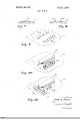
- FIG. 1is a schematic representation of one particular arrangement in accordance with the invention.
- FIG. 2is an enlarged view of a portion of the arrangement shown in FIG. 1;
- FIG. 3is a cross-sectional diagram illustrating the manner of interconnection of conductors in arrangements in accordance with the invention
- FIG. 4is another cross-sectional diagram illustrating a woven circuit arrangement in accordance with the invention having a multiplicity of layers of conductors woven within the fabric;
- FIG. 5is a schematic representation of an arrangement of woven conductors in accordance with the invention.
- FIG. 6is a diagram of an enlarged portion of FIG. 1 showing the juxtaposition of conductors arranged in particular cutting areas;
- FIG. 7is a diagram showing a portion of the arrangement of FIG. 6 prior to severance of the conductor
- FIG. 8is a diagram of the same portion of FIG. 6 showing the conductor after severance
- FIG. 9illustrates a portion of the section shown in FIG. 6 with the conducting tubes bent in position to receive a flat pack circuit module
- FIG. 10is a similar view showing an alternative arrangement of coupling the flat pack circuit module to corresponding conductors in woven circuit arrangements in accordance with the invention.
- FIG. 11shows still another arrangement for connecting woven circuit conductors to a flat pack circuit module
- FIG. 12is an enlarged view of a cutting area, also shown in FIG. 6, showing a number of conductors severed by burning;
- FIG. 13is a perspective view of another particular woven circuit arrangement in accordance with the invention including 8+ and ground busses;
- FIG. 14shows one particular arrangement for effecting splices of wire conductors in woven circuit arrangements of the invention
- FIG. 15shows an alternative arrangement for developing splices between woven tubes conductors in arrangements of the invention.
- FIG. 16illustrates still another arrangement for providing splices between woven wire conductors in arrangements with the invention.
- a particular woven circuit structure 10 in accordance with the inventioncomprises a frame 12 extending generally about a fabric portion 14 on which a plurality of circuit modules are arrayed.
- the circuit modules 16may be in the form of so-called flat packs.
- Such integrated circuit modulesmay comprise one or more semiconductor units together with the interconnecting leads and associated circuit components required to make up a particular module. These modules are available in various pack dimensions and configurations, but a typical IC module may be one-quarter inch by one-quarter inch, not including the space occupied by the leads extending from the package.
- woven circuit fabrics in accordance with the inventioncomprise a plurality of warp and shoot conductors interwoven with fibers of suitable insulating material also extending in orthogonal directions.
- a typical material employed for the insulating fibersis glass. It is not essential that the respective filaments, both insulating and conducting, extend orthogonally to each other. They may be woven in any manner and with any juxtaposition which develops substantial crossovers between conductors of one set and conductors of another set. This permits the weave pattern to be developed so that selected conductors of the two sets can be brought into contact with each other as desired to develop the conductor interconnections.
- the interwoven insulating fibersare so fabricated with the respective conducting filaments as to provide insulation and/or isolation between adjacent conductors except at the points where crossover interconnections are intended.
- FIG. 2which is an enlarged portion of woven fabric 14
- sectionsare shown on both the right-hand and lefthand sides of the figure in which horizontally extending conductors 20 are floated" to lie on top of the interwoven fabric.
- the shoot or fill conductors 20are interwoven in the fabric which also contains the warp conductors that are lifted over the shoot conductors 20 at nodal points such as 22 to provide contact between particular pairs of warp and shoot conductors, thus establishing electrical connection at the respective nodal points 22.
- FIG. 3is looking end on at filaments 20 extending in the fill direction and shows a warp conductor 24 extending upwardly from its normal plane to pass around a fill conductor 20' at a nodal point 22 to establish a desired electrical connection between the two conductors 24 and 20 at that point.
- a suitable spacingis maintained between the till conductors and the plane of the warp conductors with both warp and fill insulating fibers 26 and 28 respectively interwoven between the two planes to maintain the desired insulation therebetween.
- Similar spacing and separationis provided between adjacent pairs of fill wires and also between adjacent pairs of warp conductors.
- the entire fabricis tied together by fill binder insulating fibers such as 30.
- FIG. 4A similar woven circuit pattern is depicted in FIG. 4, differing from FIG. 3 in that a multiple layer arrangement having a plurality of layers of the fill conductors 20 and 21 is provided. Individual warp conductors 24 are taken out of the warp conductor plane in either direction to establish nodal connection points such as 22 and 23 at selected upper and lower fill conductors 20 and 21 respectively. Additional layers of conductors and associated insulating fibers may be woven in a single direction in a unitary fabric as needed to accommodate the desired density of associated circuit modules or other components.
- one of the fill conductor planesmay comprise an interwoven ground plane to which connections from the warp conductor plane may be established or omitted as desired. Such an arrangement may provide improved shielding, for example, in particular applications.
- FIG. 5The details of a particular woven circuit configuration are represented schematically in FIG. 5 in which the insulating filler fibers have been omitted for better clarity.
- a plurality of small hollow tubes 32are shown running in the fill direction, interwoven with solid conducting wires 34 extending in the warp direction. Additional fill wires 36 are interspersed between adjacent tubes 32.
- a connectioncan be established between any warp conductor 34 and fill conductor, either a wire 36 or a tube 32, by establishing a nodal point where the selected conductors cross.
- a connectioncan be established between any pair of conductors extending in the fill direction or extending in the warp direction by developing two suitably placed nodal points which serve to connect the two selected conductors to a single conductor extending in the orthogonal direction.
- the tubes 32are provided to permit ready connection to associated circuit components having external pins.
- the respective solid wires 36are interspersed between the tubes for providing additional facility in circuit connections.
- the solid wires 34 and 36are of copper and may vary from 0.001 to 0.050 inch in diameter.
- the warp and fill conductorsare typically spaced 0.1 inch on centers.
- the inside diameter of the tubes 32is chosen to fit the outside diameter of the component leads to which connection is to be established.
- FIG. 6shows a typical float pattern in the vicinity of a single circuit module.
- FIG. 6represents an enlarged pattern corresponding to that shown in FIG. 5.
- Floated fill wires 36 in the central region of FIG. 6are cut prior to module insertion.
- Selected warp wires 34are floated in the periphery of the module to permit cutting as desired.
- the two tubes 32are floated also along the periphery of the module for cutting in that region.
- the respective connecting wires 34 and 36are cut and interconnected with each other and with tubes 32 on a selective basis to develop the desired external connections from one circuit module to the next without establishing short circuits along wires which are not to be repeated from one module to the next.
- FIG. 7is an enlarged view of one particular tube 32 floated above the associated fabric 14.
- FIG. 8shows the same floated tube 32 after the cutting step which severs the tube 32 and develops a spacing between the severed ends 320 and 32b.
- Floated solid wiressuch as 34 and 36 may also be severed in similar fashion.
- FIG. 9shows a plurality of tubes 32 after the cutting process to form the severed ends 32a and 32b which are bent upward from the fabric 14 in position to receive the leads of a typical circuit module of the dual-in-line type having solid terminal leads with suitable dimensions for insertion into the tubes 320 or 32b.
- final electrical and mechanical connectionmay be made by crimping the respective tubes onto the module leads inserted therein or by known dip-soldering methods.
- Circuit 10depicts a dual-in-line package 42 having such leads 44.
- Conductors 46 for connection to the leads 44are shown positioned in alignment therewith.
- the connectors 46may in this instance be either tubes or solid wires, generally extending in the fill direction of the woven fabric 14.
- the module 42is moved downwardly toward the fabric 14 so that the leads 44 encompass corresponding ends of conductors 46.
- the terminals 44may be crimped with the final electrical and mechanical connection or such connection may be established with a soldering step.
- FIG. 11shows still another interconnecting arrangement.
- a module 42is shown positioned for a connection tors 56in a manner to make contact therewith. Thereafter, the entire structure is dip soldered to complete the electrical and mechanical connection step.
- FIG. 12depicts an enlarged view of a portion of a woven circuit fabric in accordance with the invention showing the floated conductors after they have been severed.
- the severed ends 32a and 32b of the floated conductors of FIG. 12have been severed by burning. This can be accomplished effectively by a high-temperature gas torch, for example, which effectively cuts through and melts back a portion of the floated wires without affecting the woven fabric 14 which itself is composed mainly of a high-temperature melting material such as glass fibers.
- the severed ends 324 and 32b of FIG. 12are now ready for attachment to particular circuit module in the manner shown in FIG. 10, for example.
- the conductors to be severedcomprise the tubes such as 32a and 32b of FIG. 9, the desired severance and separation are readily accomplished by the use of a grinder at sufficiently high speed and of the proper material such that the tubes are severed without filling or otherwise varying the hole within the center of the tube.
- FIG. 13illustrates another particular arrangement in accordance with the invention similar to that shown in FIG. 1 except that the frame of the woven circuit configuration is comprised of heavy conductors which may be used as busses.
- a fabric I4is woven between a pair of heavy conductors 58 and 59.
- the conductors 59may advantageously be of approximately 0.1 inch diameter copper wire as compared with the fill wires such as 36 of only a few thousands of an inch in diameter.
- the larger copper wires such as 58 and 59serve to provide some rigidity and strength to the structure of the woven circuit, but also advantageously have the capacity to carry the current which is necessary to operate effectively the many circuit modules coupled into the woven circuit conductors of the fabric 14.
- a typical circuit moduleutilizes approximately 20 milliamperes of current for normal operation.
- a woven circuit structureof any substantial dimension, particularly one where the length may run to several feet, a significant current is required to be brought to and from an associated power supply in order to operate all of the various individual circuit components.
- Thisis effectively realized by a structure such as that shown in FIG. 13in which the conductor 58 may serve as a 8+ buss and the conductor 59 may be connected as the ground return or B- buss.
- the fill wires such as 36are interwoven with the conductors 58 and 59 and the remainder of the woven fabric 14 by weaving back and forth in the normal manner. Thereafter, isolation between the bus conductors 58 and 59 is effected by cutting all of the till wires at one or more points so as to eliminate the short circuit between the conductors 58 and 59.
- FIGS. l4, l5, and 16show alternative arrangements for effecting splices in circuit arrangements in accordance with the invention.
- FIG. 14shows a tube 60 which may be used to patch together a pair of wires 62. As is indicated, the inside diameter of the hollow tube 60 is slightly greater than the outside diameter of the wires 62. The tube 60 is slipped over one of the wires 62 and the other wire 62 is inserted from the opposite end. The circuit elements 60 and 62 may be fastened together by crimping or soldering as desired.
- FIG. 15shows a corresponding arrangement for effecting a splice between a pair of hollow conducting tubes 64.
- a splicemay be effected by inserting a pin 66 within the adjacent ends of the two tubes 64, after which the tubes may be crimped to provide a good mechanical and electrical junction with the pin 66, or the connection may be completed by soldering.
- FIG. 16shows a variation of the arrangement of FIG. 14 wherein a hollow cylinder 68 is fabricated with a spring 69 contained therein.
- the cylinder 68is provided with openings at its opposite ends of a dimension such as to accommodate the insertion of a pair of wires 62.
- the loosely coiled spring 69 and the manner of its confinement within the cylinder 68permit ready insertion of the wires 62 but effectively grip the wires 62 and provide the desired electrical connection while preventing withdrawal of the wire 62 from the cylinder 68.
- Woven circuit arrangementssuch as those which have been described hereinabove may be effectively fabricated on a loom with a Jacquard head.
- Such loomsare well known, having changed very little in their structure and mode of operation in the 150 years which they have been in use.
- the Jacquard headis card controlled and may be programmed to develop any desired pattern for the woven circuit, thus establishing any interconnections between warp and fill conductors as desired.
- a typical woven circuit having a planar configuration of approximately 20 inches on a sidecan be woven on such a loom in approximately 4 minutes.
- Such a woven circuit planecan be fabricated with 0.01 inch diameter wire conductors, the wires being 0.025 inch on centers.
- the cost of weaving such a circuit planeis approximately $5.00 and the cost of all the materials (wires, tubes and insulated filaments) is approximately $25.00. This compares with the cost of comparable circuitry prepared by conventional techniques of approximately 20 times the cost of the woven circuit.
- An additional advantageis the possibility of weaving the frame to hold the woven circuit at the same time that the circuit is fabricated.
- the conductors employedmay be bare copper or they may be pretinned. In the latter case, the interconnections in the woven circuit and the connections from the circuit module terminals to the woven circuit tubes can be completed in one step by a dip-solder, hot fat dip, or induction heating bake in approximately 20 seconds.
- the respective signal conductorsmay be woven in parallel for signal and return.
- inductance of the signal wireswill be constant in terms of characteristics so that the signal lines may be treated as transmission lines.
- a woven circuit configurationincluding a plurality of circuit modules having perpendicularly depending terminals comprising:
- first and second pluralities of electrical conducting filamentsinterwoven in a fabric with a plurality of insulating fibers, the insulating fibers being situated so as to separate and insulate each filament from the rest;
- each of the filaments of a float patternhaving severed and bent free ends extending at a substantial angle to said fabric and aligned with the perpendicularly depending temtinals of the respective associated circuit module connected thereto, each of the aligned terminals and filaments engaging the other in a mating relationship, at least some of the filaments of said first plurality comprising small hollow con ducting tubes, the free ends of which receive the respective terminals of a circuit module connected thereto.
- Apparatus in accordance with claim 1further including at least a pair of conductors of substantially greater diameter than the diameter of the filaments of said first and second pluralities interwoven with filaments of one plurality along corresponding sides of the fabric so as to provide a supporting frame therefor and for carrying current to and from the woven circuit structure.
- a woven circuit configuration including a plurality of circuit components having perpendicularly depending leadscomprising:
- connection meansestablishing connections between selected ones of said filaments and said circuit components including predetermined loop patterns of said selected filaments which are cut and bent and extend at a substantial angle relative to said fabric and mate with respective ones of the perpendicularly depending leads of components, the filaments mating with the component leads comprising hollow tubular members open at the ends thereof and receiving said component leads therein.
- Apparatus in accordance with claim 6further including a third layer of conducting filaments interwoven with the insulating fibers in said fabric so as to be electrically isolated from each other and extending generally parallel to the filaments of said first layer.
- Apparatus in accordance with claim 7further including means selectively establishing connections between filaments of said third and second layers at points of crossing thereof.
- a woven circuit configuration including a plurality of circuit components having perpendicularly depending leadscomprising:
- connection meansestablishing connections between selected ones of said filaments and said circuit components including predetermined loop patterns of said selected filaments which are cut and bent and extend at a substantial angle relative to said fabric and mate with respective ones of the perpendicularly depending leads of said components;
- said configurationfurther including means electrically and mechanically joining severed filaments comprising a member mating with the respective severed ends of the filaments, said severed filaments comprising hollow tubes and said member comprising a pin extending into the ends of a pair of tubes.
- a woven circuit configurationincluding a plurality of circuit modules having depending terminals comprising:
- first and second pluralities of electrical conducting filamentsinterwoven in a fabric with a plurality of insulating fibers, the insulating fibers being situated so as to separate and insulate each filament from the rest;
Landscapes
- Engineering & Computer Science (AREA)
- Microelectronics & Electronic Packaging (AREA)
- Textile Engineering (AREA)
- Woven Fabrics (AREA)
Abstract
Description
Claims (11)
Applications Claiming Priority (1)
| Application Number | Priority Date | Filing Date | Title |
|---|---|---|---|
| US86902969A | 1969-10-24 | 1969-10-24 |
Publications (1)
| Publication Number | Publication Date |
|---|---|
| US3631298Atrue US3631298A (en) | 1971-12-28 |
Family
ID=25352805
Family Applications (1)
| Application Number | Title | Priority Date | Filing Date |
|---|---|---|---|
| US869029AExpired - LifetimeUS3631298A (en) | 1969-10-24 | 1969-10-24 | Woven interconnection structure |
Country Status (1)
| Country | Link |
|---|---|
| US (1) | US3631298A (en) |
Cited By (51)
| Publication number | Priority date | Publication date | Assignee | Title |
|---|---|---|---|---|
| US3780430A (en)* | 1972-09-25 | 1973-12-25 | Bowmar Ali Inc | Process for mounting electro-luminescent displays |
| DE2717254A1 (en)* | 1976-04-19 | 1977-11-10 | Danilin | ELECTRIC FABRIC CONTROL MATRIX |
| US4350580A (en)* | 1980-04-25 | 1982-09-21 | Olin Corporation | Current distributors for reticulate electrodes |
| US4518661A (en)* | 1982-09-28 | 1985-05-21 | Rippere Ralph E | Consolidation of wires by chemical deposition and products resulting therefrom |
| US4606968A (en)* | 1983-07-25 | 1986-08-19 | Stern And Stern Textiles, Inc. | Electrostatic dissipating fabric |
| US4971564A (en)* | 1988-04-15 | 1990-11-20 | Ferdie Meyer | Method and article used for connecting electronic components |
| US6210771B1 (en)* | 1997-09-24 | 2001-04-03 | Massachusetts Institute Of Technology | Electrically active textiles and articles made therefrom |
| US6209776B1 (en)* | 1992-08-26 | 2001-04-03 | Sanyo Electric Co., Ltd. | Flyback transformer device and process for preparing same |
| WO2001030123A1 (en)* | 1999-10-18 | 2001-04-26 | Massachusetts Institute Of Technology | Flexible electronic circuitry and method of making same |
| WO2002032665A1 (en)* | 2000-10-16 | 2002-04-25 | Foster-Miller, Inc. | A method of manufacturing a fabric article to include electronic circuitry and an electrically active textile article |
| US20030081394A1 (en)* | 2001-10-31 | 2003-05-01 | Noritsugu Enomoto | Electronic-part mounting structure and mounting method therefor |
| US20030134525A1 (en)* | 2002-01-15 | 2003-07-17 | Matthew Sweetland | Woven multiple-contact connector |
| WO2003059101A1 (en)* | 2002-01-21 | 2003-07-24 | Infineon Technologies Ag | Method and device for integrating electronics in textiles |
| US6599561B2 (en)* | 2001-11-30 | 2003-07-29 | Kulicke & Soffa Investments, Inc. | Method for manufacturing a printed circuit board substrate |
| US20030211797A1 (en)* | 2002-05-10 | 2003-11-13 | Hill Ian Gregory | Plural layer woven electronic textile, article and method |
| US20040005793A1 (en)* | 2002-01-15 | 2004-01-08 | Tribotek, Inc. | Multiple-contact woven power connectors |
| US20040009729A1 (en)* | 2002-05-10 | 2004-01-15 | Hill Ian Gregory | Woven electronic textile, yarn and article |
| US20040009693A1 (en)* | 2002-01-15 | 2004-01-15 | Tribotek, Inc. | Multiple-contact cable connector assemblies |
| US20040012937A1 (en)* | 2002-07-18 | 2004-01-22 | Kulicke & Soffa Investments, Inc. | Method for manufacturing a printed circuit board substrate with passive electrical components |
| US20040048500A1 (en)* | 2002-01-15 | 2004-03-11 | Tribotek, Inc. | Woven multiple-contact connectors |
| WO2004076731A1 (en)* | 2003-02-21 | 2004-09-10 | Infineon Technologies Ag | Textile fabric structure, surface covering structure and method for determining the interspacing of microelectronic elements of the textile fabric structure with respect to at least one reference position |
| US20040214454A1 (en)* | 2002-01-15 | 2004-10-28 | Tribotek, Inc. | Method and apparatus for manufacturing woven connectors |
| US20040259391A1 (en)* | 2001-12-14 | 2004-12-23 | Infineon Technologies Ag | Construction and connection technique in textile structures |
| US20050014421A1 (en)* | 2003-07-14 | 2005-01-20 | Tribotek, Inc. | System and methods for connecting electrical components |
| US20050045461A1 (en)* | 2003-07-11 | 2005-03-03 | Tribotek, Inc. | Multiple-contact woven electrical switches |
| WO2005031550A1 (en)* | 2003-09-24 | 2005-04-07 | Infineon Technologies Ag | Processor array, fabric structure, surface-covering structure, and method for transmitting electricity among a plurality of adjacent processor elements |
| US20050073473A1 (en)* | 2003-09-16 | 2005-04-07 | Carpinelli Joseph M. | Segmented character display |
| US20050159028A1 (en)* | 2002-01-15 | 2005-07-21 | Tribotek, Inc. | Contact woven connectors |
| US20050202695A1 (en)* | 2002-01-15 | 2005-09-15 | Tribotek, Inc. | Electrical connector |
| US20060211295A1 (en)* | 2005-03-15 | 2006-09-21 | Tribotek, Inc. | Electrical connector having one or more electrical contact points |
| US20070015387A1 (en)* | 2005-07-18 | 2007-01-18 | Tribotek, Inc. | Electrical connector |
| WO2006129272A3 (en)* | 2005-05-31 | 2007-02-08 | Koninkl Philips Electronics Nv | A fully textile electrode lay-out allowing passive and active matrix addressing |
| US20080205020A1 (en)* | 2007-02-26 | 2008-08-28 | Siemens Vdo Automotive Corporation | Connection of wire to a lead frame |
| WO2009050629A1 (en)* | 2007-10-16 | 2009-04-23 | Koninklijke Philips Electronics N.V. | Multi-layer woven fabric display |
| WO2009053872A1 (en)* | 2007-10-26 | 2009-04-30 | Koninklijke Philips Electronics N.V. | Robust connections in a multi-layer woven fabric |
| US7559902B2 (en) | 2003-08-22 | 2009-07-14 | Foster-Miller, Inc. | Physiological monitoring garment |
| US20100071205A1 (en)* | 2008-09-22 | 2010-03-25 | David Graumann | Method and apparatus for attaching chip to a textile |
| EP2206813A1 (en)* | 2009-01-09 | 2010-07-14 | Strähle + Hess GmbH | Conductive textile and interior component for motor vehicles with a conductive textile |
| US20110036448A1 (en)* | 2008-04-29 | 2011-02-17 | Koninklijke Philips Electronics N.V. | Electronic textile |
| US20110122591A1 (en)* | 2008-07-08 | 2011-05-26 | Martyn John Hucker | Hybrid fabric materials, and structural components incorporating same |
| CN102181987A (en)* | 2011-04-07 | 2011-09-14 | 东华大学 | Novel fabric display |
| WO2012145865A1 (en)* | 2011-04-29 | 2012-11-01 | Yang Chang-Ming | Method for electronizing cloth and its product |
| US8585606B2 (en) | 2010-09-23 | 2013-11-19 | QinetiQ North America, Inc. | Physiological status monitoring system |
| US20150077910A1 (en)* | 2013-09-13 | 2015-03-19 | Lenovo (Beijing) Limited | Manufacturing method of housing and electronic device |
| US9028404B2 (en) | 2010-07-28 | 2015-05-12 | Foster-Miller, Inc. | Physiological status monitoring system |
| US9119916B2 (en) | 2010-03-23 | 2015-09-01 | Fresenius Medical Care Deutschland Gmbh | Device for detecting moisture for use with a device for monitoring an access to a patient, in particular for monitoring the vascular access in an extracorporeal blood treatment |
| US9211085B2 (en) | 2010-05-03 | 2015-12-15 | Foster-Miller, Inc. | Respiration sensing system |
| US9782096B2 (en) | 2011-01-31 | 2017-10-10 | Clothing Plus Mbu Oy | Textile substrate for measuring physical quantity |
| US10886680B2 (en) | 2014-12-19 | 2021-01-05 | Intel Corporation | Snap button fastener providing electrical connection |
| US11291409B2 (en) | 2014-12-03 | 2022-04-05 | Clothing Plus Mbu Oy | Device for determining effects of aging of a wearable device |
| US11436900B2 (en) | 2014-09-23 | 2022-09-06 | Intel Corporation | Apparatus and methods for haptic covert communication |
Citations (7)
| Publication number | Priority date | Publication date | Assignee | Title |
|---|---|---|---|---|
| DE1082641B (en)* | 1959-03-11 | 1960-06-02 | Standard Elektrik Lorenz Ag | Woven electrical ribbon cable, especially for multiple wiring |
| DE1085207B (en)* | 1959-08-28 | 1960-07-14 | Siemens Ag | Carrier for electrical components to be wired |
| DE1175761B (en)* | 1962-02-05 | 1964-08-13 | Dr Eberhard Tebbenhoff | Electrical circuit in the form of a fabric |
| US3160790A (en)* | 1962-04-06 | 1964-12-08 | Mittler Sheldon | Tubular electric circuits and component mounted thereon |
| US3371250A (en)* | 1966-03-09 | 1968-02-27 | Southern Weaving Co | Woven circuit device |
| US3447120A (en)* | 1967-06-05 | 1969-05-27 | Southern Weaving Co | Woven high-frequency transmission line |
| US3479565A (en)* | 1967-09-06 | 1969-11-18 | Southern Weaving Co | Woven circuit device |
- 1969
- 1969-10-24USUS869029Apatent/US3631298A/ennot_activeExpired - Lifetime
Patent Citations (7)
| Publication number | Priority date | Publication date | Assignee | Title |
|---|---|---|---|---|
| DE1082641B (en)* | 1959-03-11 | 1960-06-02 | Standard Elektrik Lorenz Ag | Woven electrical ribbon cable, especially for multiple wiring |
| DE1085207B (en)* | 1959-08-28 | 1960-07-14 | Siemens Ag | Carrier for electrical components to be wired |
| DE1175761B (en)* | 1962-02-05 | 1964-08-13 | Dr Eberhard Tebbenhoff | Electrical circuit in the form of a fabric |
| US3160790A (en)* | 1962-04-06 | 1964-12-08 | Mittler Sheldon | Tubular electric circuits and component mounted thereon |
| US3371250A (en)* | 1966-03-09 | 1968-02-27 | Southern Weaving Co | Woven circuit device |
| US3447120A (en)* | 1967-06-05 | 1969-05-27 | Southern Weaving Co | Woven high-frequency transmission line |
| US3479565A (en)* | 1967-09-06 | 1969-11-18 | Southern Weaving Co | Woven circuit device |
Cited By (104)
| Publication number | Priority date | Publication date | Assignee | Title |
|---|---|---|---|---|
| US3780430A (en)* | 1972-09-25 | 1973-12-25 | Bowmar Ali Inc | Process for mounting electro-luminescent displays |
| DE2717254A1 (en)* | 1976-04-19 | 1977-11-10 | Danilin | ELECTRIC FABRIC CONTROL MATRIX |
| US4158103A (en)* | 1976-04-19 | 1979-06-12 | Danilin Jurij Ivanovic | Electric woven switching matrix |
| US4350580A (en)* | 1980-04-25 | 1982-09-21 | Olin Corporation | Current distributors for reticulate electrodes |
| US4518661A (en)* | 1982-09-28 | 1985-05-21 | Rippere Ralph E | Consolidation of wires by chemical deposition and products resulting therefrom |
| US4606968A (en)* | 1983-07-25 | 1986-08-19 | Stern And Stern Textiles, Inc. | Electrostatic dissipating fabric |
| US4971564A (en)* | 1988-04-15 | 1990-11-20 | Ferdie Meyer | Method and article used for connecting electronic components |
| US6209776B1 (en)* | 1992-08-26 | 2001-04-03 | Sanyo Electric Co., Ltd. | Flyback transformer device and process for preparing same |
| US6210771B1 (en)* | 1997-09-24 | 2001-04-03 | Massachusetts Institute Of Technology | Electrically active textiles and articles made therefrom |
| US6493933B1 (en) | 1999-10-18 | 2002-12-17 | Massachusetts Institute Of Technology | Method of making flexible electronic circuitry |
| WO2001030123A1 (en)* | 1999-10-18 | 2001-04-26 | Massachusetts Institute Of Technology | Flexible electronic circuitry and method of making same |
| WO2002032665A1 (en)* | 2000-10-16 | 2002-04-25 | Foster-Miller, Inc. | A method of manufacturing a fabric article to include electronic circuitry and an electrically active textile article |
| JP2004513247A (en)* | 2000-10-16 | 2004-04-30 | フォスター−ミラー・インク | Method for producing a textile product with electronic circuitry and an electrically active textile product |
| US6729025B2 (en) | 2000-10-16 | 2004-05-04 | Foster-Miller, Inc. | Method of manufacturing a fabric article to include electronic circuitry and an electrically active textile article |
| US20030081394A1 (en)* | 2001-10-31 | 2003-05-01 | Noritsugu Enomoto | Electronic-part mounting structure and mounting method therefor |
| US6599561B2 (en)* | 2001-11-30 | 2003-07-29 | Kulicke & Soffa Investments, Inc. | Method for manufacturing a printed circuit board substrate |
| US7022917B2 (en)* | 2001-12-14 | 2006-04-04 | Infineon Technologies Ag | Construction and electrical connection technique in textile structures |
| US20040259391A1 (en)* | 2001-12-14 | 2004-12-23 | Infineon Technologies Ag | Construction and connection technique in textile structures |
| US20040214454A1 (en)* | 2002-01-15 | 2004-10-28 | Tribotek, Inc. | Method and apparatus for manufacturing woven connectors |
| US20060063413A1 (en)* | 2002-01-15 | 2006-03-23 | Tribotek, Inc. | Electrical connector |
| US6951465B2 (en) | 2002-01-15 | 2005-10-04 | Tribotek, Inc. | Multiple-contact woven power connectors |
| US20040048500A1 (en)* | 2002-01-15 | 2004-03-11 | Tribotek, Inc. | Woven multiple-contact connectors |
| US7101194B2 (en) | 2002-01-15 | 2006-09-05 | Tribotek, Inc. | Woven multiple-contact connector |
| US20040005793A1 (en)* | 2002-01-15 | 2004-01-08 | Tribotek, Inc. | Multiple-contact woven power connectors |
| US20040171284A1 (en)* | 2002-01-15 | 2004-09-02 | Tribotek, Inc. | Woven multiple-contact connector |
| US7083427B2 (en) | 2002-01-15 | 2006-08-01 | Tribotek, Inc. | Woven multiple-contact connectors |
| US7223111B2 (en) | 2002-01-15 | 2007-05-29 | Tribotek, Inc. | Electrical connector |
| US6945790B2 (en) | 2002-01-15 | 2005-09-20 | Tribotek, Inc. | Multiple-contact cable connector assemblies |
| US7077662B2 (en) | 2002-01-15 | 2006-07-18 | Tribotek, Inc. | Contact woven connectors |
| US20050202695A1 (en)* | 2002-01-15 | 2005-09-15 | Tribotek, Inc. | Electrical connector |
| US20060134943A1 (en)* | 2002-01-15 | 2006-06-22 | Tribotek, Inc. | Contact woven connectors |
| US7056139B2 (en) | 2002-01-15 | 2006-06-06 | Tribotek, Inc. | Electrical connector |
| US20030134525A1 (en)* | 2002-01-15 | 2003-07-17 | Matthew Sweetland | Woven multiple-contact connector |
| US7021957B2 (en) | 2002-01-15 | 2006-04-04 | Tribotek, Inc. | Woven multiple-contact connector |
| US20040009693A1 (en)* | 2002-01-15 | 2004-01-15 | Tribotek, Inc. | Multiple-contact cable connector assemblies |
| US6942496B2 (en) | 2002-01-15 | 2005-09-13 | Tribotek, Inc. | Woven multiple-contact connector |
| US20050130486A1 (en)* | 2002-01-15 | 2005-06-16 | Tribotek, Inc. | Woven multiple-contact connector |
| US20050159028A1 (en)* | 2002-01-15 | 2005-07-21 | Tribotek, Inc. | Contact woven connectors |
| JP2005514537A (en)* | 2002-01-21 | 2005-05-19 | インフィネオン テクノロジーズ アクチエンゲゼルシャフト | Method and apparatus for electrical integration in textiles |
| US20050029680A1 (en)* | 2002-01-21 | 2005-02-10 | Infineon Technologies Ag | Method and apparatus for the integration of electronics in textiles |
| WO2003059101A1 (en)* | 2002-01-21 | 2003-07-24 | Infineon Technologies Ag | Method and device for integrating electronics in textiles |
| EP1507906A4 (en)* | 2002-05-10 | 2006-08-23 | Sarnoff Corp | MULTILAYER WOVEN TEXTILE PRODUCT WITH WOVEN ELECTRONIC CIRCUIT, AND CORRESPONDING METHOD |
| US20050081944A1 (en)* | 2002-05-10 | 2005-04-21 | Carpinelli Joseph M. | Display having addressable characters |
| US20030211797A1 (en)* | 2002-05-10 | 2003-11-13 | Hill Ian Gregory | Plural layer woven electronic textile, article and method |
| US7144830B2 (en) | 2002-05-10 | 2006-12-05 | Sarnoff Corporation | Plural layer woven electronic textile, article and method |
| US7592276B2 (en) | 2002-05-10 | 2009-09-22 | Sarnoff Corporation | Woven electronic textile, yarn and article |
| US20090253325A1 (en)* | 2002-05-10 | 2009-10-08 | Philadelphia Univesrsity | Plural layer woven electronic textile, article and method |
| US20040009729A1 (en)* | 2002-05-10 | 2004-01-15 | Hill Ian Gregory | Woven electronic textile, yarn and article |
| US20040012937A1 (en)* | 2002-07-18 | 2004-01-22 | Kulicke & Soffa Investments, Inc. | Method for manufacturing a printed circuit board substrate with passive electrical components |
| US20060035554A1 (en)* | 2003-02-21 | 2006-02-16 | Infineon Technologies Ag | Textile fabric structure |
| WO2004076731A1 (en)* | 2003-02-21 | 2004-09-10 | Infineon Technologies Ag | Textile fabric structure, surface covering structure and method for determining the interspacing of microelectronic elements of the textile fabric structure with respect to at least one reference position |
| US20050045461A1 (en)* | 2003-07-11 | 2005-03-03 | Tribotek, Inc. | Multiple-contact woven electrical switches |
| US7094064B2 (en) | 2003-07-11 | 2006-08-22 | Tribotek, Inc. | Multiple-contact woven electrical switches |
| GB2419477A (en)* | 2003-07-14 | 2006-04-26 | Tribotek Inc | Systems and methods for connecting electrical components |
| US7097495B2 (en) | 2003-07-14 | 2006-08-29 | Tribotek, Inc. | System and methods for connecting electrical components |
| US20050014421A1 (en)* | 2003-07-14 | 2005-01-20 | Tribotek, Inc. | System and methods for connecting electrical components |
| WO2005009096A3 (en)* | 2003-07-14 | 2005-02-24 | Tribotek Inc | Systems and methods for connecting electrical components |
| US7125281B2 (en) | 2003-07-14 | 2006-10-24 | Tribotek, Inc. | Systems and methods for connecting electrical components |
| GB2419477B (en)* | 2003-07-14 | 2007-05-09 | Tribotek Inc | Systems and methods for connecting electrical components |
| CN100573159C (en)* | 2003-07-14 | 2009-12-23 | 迈索德电子公司 | System and method for connecting electrical components |
| US20050239329A1 (en)* | 2003-07-14 | 2005-10-27 | Tribotek, Inc. | Systems and methods for connecting electrical components |
| US7559902B2 (en) | 2003-08-22 | 2009-07-14 | Foster-Miller, Inc. | Physiological monitoring garment |
| US7324071B2 (en) | 2003-09-16 | 2008-01-29 | Sarnoff Corporation | Segmented character display |
| US20050073473A1 (en)* | 2003-09-16 | 2005-04-07 | Carpinelli Joseph M. | Segmented character display |
| US20070192647A1 (en)* | 2003-09-24 | 2007-08-16 | Rupert Glaser | Process array, fabric structure, surface-covering structure and method of transmitting electricity |
| US7941676B2 (en) | 2003-09-24 | 2011-05-10 | Infineon Technologies Ag | Processor array having a multiplicity of processor elements and method of transmitting electricity between processor elements |
| WO2005031550A1 (en)* | 2003-09-24 | 2005-04-07 | Infineon Technologies Ag | Processor array, fabric structure, surface-covering structure, and method for transmitting electricity among a plurality of adjacent processor elements |
| US7140916B2 (en) | 2005-03-15 | 2006-11-28 | Tribotek, Inc. | Electrical connector having one or more electrical contact points |
| US20060211295A1 (en)* | 2005-03-15 | 2006-09-21 | Tribotek, Inc. | Electrical connector having one or more electrical contact points |
| WO2006129272A3 (en)* | 2005-05-31 | 2007-02-08 | Koninkl Philips Electronics Nv | A fully textile electrode lay-out allowing passive and active matrix addressing |
| US20080196783A1 (en)* | 2005-05-31 | 2008-08-21 | Koninklijke Philips Electronics, N.V. | Fully Textile Electrode Lay-Out Allowing Passive and Active Matrix Addressing |
| US7214106B2 (en) | 2005-07-18 | 2007-05-08 | Tribotek, Inc. | Electrical connector |
| US7458827B2 (en) | 2005-07-18 | 2008-12-02 | Methode Electronics, Inc. | Electrical connector |
| US20070015419A1 (en)* | 2005-07-18 | 2007-01-18 | Tribotek, Inc. | Electrical connector |
| US20070015387A1 (en)* | 2005-07-18 | 2007-01-18 | Tribotek, Inc. | Electrical connector |
| US7837494B2 (en)* | 2007-02-26 | 2010-11-23 | Continental Automotive Systems Us, Inc. | Connection of wire to a lead frame |
| US20080205020A1 (en)* | 2007-02-26 | 2008-08-28 | Siemens Vdo Automotive Corporation | Connection of wire to a lead frame |
| WO2009050629A1 (en)* | 2007-10-16 | 2009-04-23 | Koninklijke Philips Electronics N.V. | Multi-layer woven fabric display |
| US20100208445A1 (en)* | 2007-10-16 | 2010-08-19 | Koninklijke Philips Electronics N.V. | Multi-layer woven fabric display |
| WO2009053872A1 (en)* | 2007-10-26 | 2009-04-30 | Koninklijke Philips Electronics N.V. | Robust connections in a multi-layer woven fabric |
| US20110036448A1 (en)* | 2008-04-29 | 2011-02-17 | Koninklijke Philips Electronics N.V. | Electronic textile |
| AU2009269881B2 (en)* | 2008-07-08 | 2014-09-11 | Bae Systems Plc | Hybrid fabric materials. and structural components incorporating same |
| US20110122591A1 (en)* | 2008-07-08 | 2011-05-26 | Martyn John Hucker | Hybrid fabric materials, and structural components incorporating same |
| AU2009269881B9 (en)* | 2008-07-08 | 2014-10-30 | Bae Systems Plc | Hybrid fabric materials. and structural components incorporating same |
| US20100071205A1 (en)* | 2008-09-22 | 2010-03-25 | David Graumann | Method and apparatus for attaching chip to a textile |
| US20180187347A1 (en)* | 2008-09-22 | 2018-07-05 | Intel Corporation | Method and apparatus for attaching chip to a textile |
| US9758907B2 (en)* | 2008-09-22 | 2017-09-12 | Intel Corporation | Method and apparatus for attaching chip to a textile |
| EP2206813A1 (en)* | 2009-01-09 | 2010-07-14 | Strähle + Hess GmbH | Conductive textile and interior component for motor vehicles with a conductive textile |
| US9867934B2 (en) | 2010-03-23 | 2018-01-16 | Fresenius Medical Care Deutschland Gmbh | Device for detecting moisture for use with a device for monitoring an access to a patient, in particular for monitoring the vascular access in an extracorporeal blood treatment |
| US9119916B2 (en) | 2010-03-23 | 2015-09-01 | Fresenius Medical Care Deutschland Gmbh | Device for detecting moisture for use with a device for monitoring an access to a patient, in particular for monitoring the vascular access in an extracorporeal blood treatment |
| US9211085B2 (en) | 2010-05-03 | 2015-12-15 | Foster-Miller, Inc. | Respiration sensing system |
| US9028404B2 (en) | 2010-07-28 | 2015-05-12 | Foster-Miller, Inc. | Physiological status monitoring system |
| US8585606B2 (en) | 2010-09-23 | 2013-11-19 | QinetiQ North America, Inc. | Physiological status monitoring system |
| US9782096B2 (en) | 2011-01-31 | 2017-10-10 | Clothing Plus Mbu Oy | Textile substrate for measuring physical quantity |
| US10610118B2 (en) | 2011-01-31 | 2020-04-07 | Clothing Plus Mbu Oy | Textile substrate for measuring physical quantity |
| CN102181987A (en)* | 2011-04-07 | 2011-09-14 | 东华大学 | Novel fabric display |
| WO2012145865A1 (en)* | 2011-04-29 | 2012-11-01 | Yang Chang-Ming | Method for electronizing cloth and its product |
| US20150077910A1 (en)* | 2013-09-13 | 2015-03-19 | Lenovo (Beijing) Limited | Manufacturing method of housing and electronic device |
| US9844903B2 (en)* | 2013-09-13 | 2017-12-19 | Lenovo (Beijing) Limited | Manufacturing method of housing and electronic device |
| US11436900B2 (en) | 2014-09-23 | 2022-09-06 | Intel Corporation | Apparatus and methods for haptic covert communication |
| US11291409B2 (en) | 2014-12-03 | 2022-04-05 | Clothing Plus Mbu Oy | Device for determining effects of aging of a wearable device |
| US10886680B2 (en) | 2014-12-19 | 2021-01-05 | Intel Corporation | Snap button fastener providing electrical connection |
| US11342720B2 (en) | 2014-12-19 | 2022-05-24 | Intel Corporation | Snap button fastener providing electrical connection |
| US11804683B2 (en) | 2014-12-19 | 2023-10-31 | Intel Corporation | Snap button fastener providing electrical connection |
Similar Documents
| Publication | Publication Date | Title |
|---|---|---|
| US3631298A (en) | Woven interconnection structure | |
| US3891898A (en) | Panel board mounting and interconnection system for electronic logic circuitry | |
| US3751801A (en) | Method and apparatus for terminating electrical ribbon cable | |
| US4489364A (en) | Chip carrier with embedded engineering change lines with severable periodically spaced bridging connectors on the chip supporting surface | |
| US6018866A (en) | Apparatus and method for printed circuit board repair | |
| US3378920A (en) | Method for producing an interconnection matrix | |
| CA1167976A (en) | Circuit board having encapsulatd wiring on component side | |
| US2951184A (en) | Printed wiring assembly | |
| US3643133A (en) | Wire-routing system | |
| US3824433A (en) | Universal circuit board | |
| US3591922A (en) | Fabrication of electrical solder joints using electrodeposited solder | |
| US3083261A (en) | Electrical connector for closely spaced terminals | |
| JPH03183106A (en) | Printed wiring board | |
| US3293502A (en) | Miniature dry reed relay crosspoint matrix package | |
| US3842190A (en) | Wire routing system | |
| US3470612A (en) | Method of making multilayer circuit boards | |
| US3193731A (en) | Printed matrix board assembly | |
| US3676923A (en) | Methods of producing solenoid array memories | |
| US3753046A (en) | Multi-layer printed circuit board | |
| US3631300A (en) | Circuit distribution board with wire receiving channel | |
| US3478425A (en) | Method of making an electrical assembly | |
| US3944719A (en) | Wire routing apparatus | |
| US3242384A (en) | Circuit module | |
| US3260982A (en) | Flat cable strain relief | |
| US3491197A (en) | Universal printed circuit board |
Legal Events
| Date | Code | Title | Description |
|---|---|---|---|
| AS | Assignment | Owner name:ALLIED CORPORATION COLUMBIA ROAD AND PARK AVENUE, Free format text:ASSIGNMENT OF ASSIGNORS INTEREST.;ASSIGNOR:BUNKER RAMO CORPORATION A CORP. OF DE;REEL/FRAME:004149/0365 Effective date:19820922 | |
| AS | Assignment | Owner name:EATON CORPORATION AN OH CORP Free format text:ASSIGNMENT OF ASSIGNORS INTEREST.;ASSIGNOR:ALLIED CORPORATION A NY CORP;REEL/FRAME:004261/0983 Effective date:19840426 | |
| AS | Assignment | Owner name:CONTEL FEDERAL SYSTEMS, INC., A DE CORP.,VIRGINIA Free format text:ASSIGNMENT OF ASSIGNORS INTEREST;ASSIGNOR:EATON CORPORATION, A OH CORP.;REEL/FRAME:004941/0693 Effective date:19880831 Owner name:CONTEL FEDERAL SYSTEMS, INC., CONTEL PLAZA BUILDIN Free format text:ASSIGNMENT OF ASSIGNORS INTEREST.;ASSIGNOR:EATON CORPORATION, A OH CORP.;REEL/FRAME:004941/0693 Effective date:19880831 |