US20230342897A1 - Method to detect camera blemishes - Google Patents
Method to detect camera blemishesDownload PDFInfo
- Publication number
- US20230342897A1 US20230342897A1US17/660,768US202217660768AUS2023342897A1US 20230342897 A1US20230342897 A1US 20230342897A1US 202217660768 AUS202217660768 AUS 202217660768AUS 2023342897 A1US2023342897 A1US 2023342897A1
- Authority
- US
- United States
- Prior art keywords
- data blocks
- data
- potentially bad
- digital
- data block
- Prior art date
- Legal status (The legal status is an assumption and is not a legal conclusion. Google has not performed a legal analysis and makes no representation as to the accuracy of the status listed.)
- Granted
Links
Images


Classifications
- G—PHYSICS
- G06—COMPUTING OR CALCULATING; COUNTING
- G06T—IMAGE DATA PROCESSING OR GENERATION, IN GENERAL
- G06T7/00—Image analysis
- G06T7/0002—Inspection of images, e.g. flaw detection
- G06T7/0004—Industrial image inspection
- G—PHYSICS
- G06—COMPUTING OR CALCULATING; COUNTING
- G06T—IMAGE DATA PROCESSING OR GENERATION, IN GENERAL
- G06T7/00—Image analysis
- G06T7/0002—Inspection of images, e.g. flaw detection
- G—PHYSICS
- G06—COMPUTING OR CALCULATING; COUNTING
- G06T—IMAGE DATA PROCESSING OR GENERATION, IN GENERAL
- G06T3/00—Geometric image transformations in the plane of the image
- G06T3/40—Scaling of whole images or parts thereof, e.g. expanding or contracting
- H—ELECTRICITY
- H04—ELECTRIC COMMUNICATION TECHNIQUE
- H04N—PICTORIAL COMMUNICATION, e.g. TELEVISION
- H04N17/00—Diagnosis, testing or measuring for television systems or their details
- H04N17/002—Diagnosis, testing or measuring for television systems or their details for television cameras
- G—PHYSICS
- G06—COMPUTING OR CALCULATING; COUNTING
- G06T—IMAGE DATA PROCESSING OR GENERATION, IN GENERAL
- G06T2207/00—Indexing scheme for image analysis or image enhancement
- G06T2207/10—Image acquisition modality
- G06T2207/10024—Color image
- G—PHYSICS
- G06—COMPUTING OR CALCULATING; COUNTING
- G06T—IMAGE DATA PROCESSING OR GENERATION, IN GENERAL
- G06T2207/00—Indexing scheme for image analysis or image enhancement
- G06T2207/20—Special algorithmic details
- G06T2207/20212—Image combination
- G06T2207/20216—Image averaging
- G—PHYSICS
- G06—COMPUTING OR CALCULATING; COUNTING
- G06T—IMAGE DATA PROCESSING OR GENERATION, IN GENERAL
- G06T2207/00—Indexing scheme for image analysis or image enhancement
- G06T2207/20—Special algorithmic details
- G06T2207/20212—Image combination
- G06T2207/20224—Image subtraction
Definitions
- the present disclosurerelates to camera testing. More specifically, the present invention relates to a method to detect camera blemishes in a digital camera under test, for example a camera in a mobile device such as a smart phone or tablet.
- the present disclosureprovides a test procedure that is fully automated such that a digital picture is taken of a white background by a camera under test and an algorithm is applied to determine if there are blemish defects in the camera.
- the procedure describedignores small particles in the test image to not cause false test failures.
- the disclosed methodcan detect the dust and ignore it, where other tests would detect even the smallest dust particles and return a camera failure.
- the disclosed camera blemish testadds reliability. Operators can rely on the test to determine blemishes in the device camera lens and/or camera sensor without considering small dust particles. This speeds up testing as there is no need for retesting. Also, as small particles are ignored, there is no need to remove the finest dust particles from the light used for the test image prior to each test to ensure there are no particles.
- a method of detecting a blemish in a digital cameraincludes capturing a digital image of a white area by the digital camera; reducing resolution of the digital image by grouping pixels of the digital data into a matrix of a plurality of data blocks; and comparing a luminance value of each of the plurality of data blocks to an average luminance value of other data blocks of the plurality of data blocks within a predetermined region to determine if each of the plurality of data blocks is a potentially bad data block.
- the methodcan further include determining a total number of potentially bad data blocks within a predetermined region centered around each of the potentially bad data blocks; identifying the potentially bad data block as a blemish if the total number of potentially bad data blocks around the potentially bad data block exceeds a threshold; and identifying the potentially bad data block as not a blemish if the total number of potentially bad data blocks around the potentially bad data block does not exceed the threshold.
- the pixels of the digital dataare grouped into a matrix of data blocks.
- the luminance value of each of the data blocksis calculated by averaging respective color values for red, green, and blue of all of the pixels within each data block and then using the resulting average red, average green, and average blue color values in a luminance conversion formula.
- a difference between the luminance value of each of the plurality of data blocks to the average luminance value of other data blocks of the plurality of data blocksmust exceed a predetermined value to determine if each of the plurality of data blocks is a potentially bad data block.
- a method of detecting a blemish in a digital cameraincludes capturing a digital image of a white area by the digital camera; comparing each of a plurality of data blocks that include all of the digital data of the digital image to determine if a difference in luminance values of other of the plurality of data blocks exceeds a predetermined threshold, the threshold indicating a possible blemish.
- the methodcan further include reducing the resolution of the digital image prior to the step of comparing.
- the methodcan further include identifying each of the plurality of data blocks with a luminance value that exceeds the threshold as a potentially bad data block; and totaling the number of potentially bad data blocks within a predetermined region of each potentially data block.
- FIG. 1shows a test set-up according to an embodiment of the current disclosure.
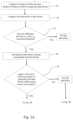
- FIG. 2 Ais a flowchart of steps according to a method of the current disclosure.
- FIG. 2 Bis a continuation of FIG. 2 A .
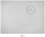
- FIG. 3is a representative test image taken of a uniformly lit white test area that includes a camera blemish.
- FIG. 4is an image showing identified potentially bad data blocks.
- FIG. 5is an image showing identified bad data blocks.
- the purpose of the disclosed method to detect camera blemishesis to be able to identify problem areas in images from digital cameras that appear as blemishes, smears, non-uniformities, or shadows in a test image taken by a digital camera. These blemishes are not smudges or other debris over camera lens, but are defects with the camera itself including the lens or the image sensor.
- the method to detect camera blemishesis designed to ignore smudges or other small defects that can be removed by cleaning the lens.
- the methodrequires taking a digital image of a uniform white test area.
- the luminance of the test areais set to an appropriate level for detecting blemishes.
- FIG. 1is a block diagram of a test apparatus used to detect blemishes of a digital camera 10 under test.
- FIG. 1shows that the digital camera 10 under test is driven by test electronics 20 to operate the camera 10 and receive and analyze a test image taken by the camera 10 .
- the test electronics 20can include a processor, memory, circuitry, and wiring to interface with the camera and a user.
- the camera 10is driven by the test electronics 20 to capture a digital test image of a uniformly lit white test area 30 .
- the white test area 30can be a diffuser panel that is backlit by a light source 40 .
- the white test area 30can be a reflective sheet that is front lit and reflects uniformly.
- the disclosed test methodis described with respect to the flowchart provided in FIG. 2 A and continued in FIG. 2 B .
- step S 1the test electronics 20 controls the digital camera 10 to take a test image of the white test area 30 and the digital data representing the test image is transmitted to the test electronics 20 .
- FIG. 3is a representative test image taken of the uniformly lit white test area 30 that includes a camera blemish shown has a non-uniform area within the overlaid dotted circle.
- the test electronicsreduces the native resolution of the test image data by reformatting the test image data into blocks of pixels where each pixel includes a red, a green, and a blue sub-pixel. Other dimensions of a data matrix are possible, but a size of 16 ⁇ 16 has been found to provide suitable blemish detection while minimizing false results caused by noise or dust particles and speeds processing.
- the data matrixis created by combining the pixels of the test image data into, for example, 16 ⁇ 16 data blocks.
- the luminance value L of each data blockis calculated by averaging the red, green, and blue color values of all of the pixels within each data block and converting the average color values into the luminance value L.
- the representative luminance value L of each data blockis calculated using a conversion formula. For example, the luminance L can equal (0.2126*R)+(0.7152*G)+(0.0722*B), where R, G, and B are the average red, green, and blue color values for the digital image pixels within the corresponding data block.
- the new lower resolution data matrixcan now contain 256 data blocks (DB1 to DB256) or regions to analyze.
- Averaging the luminance values of each 16 ⁇ 16 pixel blocknormalizes the test data and helps to sort out false failures caused by small specks of dust.
- the brightness of light reflected by small specks of dust or other contamination with the test areacan be different than the light in nearby areas causing the brightness of the dust to stand out.
- step S 2the luminance value L of each data block is compared to luminance values L of surrounding data blocks.
- the luminance values L of three consecutive data blocks some distance away from the test data block being analyzedare averaged as L avg .
- Those average luminance values L avgare compared to the luminance value of the test data block, L test .
- a data block that represents the upper left-most pixels of the test image datais being analyzed (i.e., DB1)
- its luminance value as L testcan be compared to the average luminance value L avg of data blocks that have a gap from DB1 in a horizontal right direction or vertical down direction.
- the gap between the test data block being analyzed and the data blocks averagedcan be predetermined based on the location of the data blocks in the matrix and how well the respective distances and locations of the data blocks reveal blemish defects.
- the gapcan be ten data blocks or some other number.
- the surrounding data blocks used to compare to the test data blockcan be located in the horizontal, vertical, diagonal directions, or combinations thereof.
- the luminance of a test data block that is not near the edge of the data matrixcan be compared to average luminance values of six pixels blocks on either side of the test data block.
- the first three pixel blockscan be in the same column as each other and located after the gap such that one of the pixel blocks is in the same row of the data matrix to the right of the test data block, one pixel block is in the row above, and one pixel block is in the row below.
- the luminance of these three pixelscan be averaged.
- the second three pixel blockscan be in the same column as each other and located after the gap such that one of the pixel blocks is in the same row of the data matrix to the left of the test data block, one pixel block is in the row above, and one pixel block is in the row below.
- the luminance of these three pixelscan be averaged.
- Test data blocks located near the edge of the data matrixcan be compared to average luminance values of pixels blocks to only one side of the test data block.
- step S 3a determination is made if the difference between the L test and the L avg is over a predetermined threshold. If the threshold is met, the test data block being analyzed is added to a group of potentially bad data blocks in step S 4 . If the threshold is not met, the test data block is determined not to contain a blemish.
- the threshold differenceis determined empirically by experimentation of test samples with known blemishes.
- FIG. 4is an image showing identified potentially bad data blocks 400 and 410 , marked as darker areas, overlaid on the test image shown in FIG. 3 .
- FIG. 4shows clusters of potentially bad data blocks 400 in an area with the blemish encircled in FIG. 3 .
- the potentially bad data block 410is in a location away from the blemish.
- a function named ‘clear noise’is applied to identify bad data blocks and eliminate potentially bad data blocks that have dust and other image noise that are not considered to be bad data block or blemishes. Regions around each of the potentially bad data blocks are analyzed using the ‘clear noise’ function. In order for a potentially bad data block to be considered a bad data block, it must be within a cluster of a number of other potentially bad data blocks over a predetermined number of ‘Max Defects’. For example, a group of 20 ⁇ 20 data blocks (400 total) around a potentially bad data block can be analyzed to determine how many other potentially bad data blocks are within the group.
- the potentially bad data blockis determined to be a bad data block (i.e., a blemish) and identified as such in step S 6 , and the camera fails the test. If the total number of potentially bad data blocks within the group does not meet Max Defects, then the potentially bad data block is determined not to be a bad data block.
- Max Defectsa threshold number
- FIG. 5is an image showing identified bad data blocks 500 , marked as darker areas, overlaid on the test image shown in FIG. 3 .
- the potentially bad data block 410 of FIG. 4was determined not to be a bad data block.
- FIG. 5shows five bad data blocks 500 in the area where clusters of potentially bad data blocks 400 were shown in FIG. 4 .
- the camerafails the test because bad data blocks 500 have been identified.
- step S 7a check is performed of the total overall image as a whole in step S 7 . If no blemishes are detected due to the lack of proximity of potentially bad data blocks to each other of the previously detected possible bad data blocks, but the total count of potentially bad data blocks is over a predefined number, the camera under test fails. This is in the event that too much debris or other errors occurred taking the image for a proper analysis to be performed.
- step S 8the results are reported to an inspector or test technician and recorded in a database. If any blemishes are detected during analysis, the camera is reported as a failure. Otherwise, the camera is reported to pass the blemish test.
- the above-described embodiments of the present inventioncan be implemented in any of numerous ways.
- the embodimentsmay be implemented using hardware, software or a combination thereof.
- the software codecan be executed on any suitable processor or collection of processors, whether provided in a single computer or distributed among multiple computers.
- processorsmay be implemented as integrated circuits, with one or more processors in an integrated circuit component.
- a processormay be implemented using circuitry in any suitable format.
- the above-described embodimentscan be implemented as a non-transitory computer readable storage medium embodied thereon a program executable by a processor for performing a method of various embodiments.
Landscapes
- Engineering & Computer Science (AREA)
- Physics & Mathematics (AREA)
- General Physics & Mathematics (AREA)
- Theoretical Computer Science (AREA)
- Quality & Reliability (AREA)
- Computer Vision & Pattern Recognition (AREA)
- Biomedical Technology (AREA)
- General Health & Medical Sciences (AREA)
- Multimedia (AREA)
- Signal Processing (AREA)
- Health & Medical Sciences (AREA)
- Image Analysis (AREA)
- Testing, Inspecting, Measuring Of Stereoscopic Televisions And Televisions (AREA)
Abstract
Description
- The present disclosure relates to camera testing. More specifically, the present invention relates to a method to detect camera blemishes in a digital camera under test, for example a camera in a mobile device such as a smart phone or tablet.
- During testing, operators manually check a camera picture of a digital camera under test to determine if there are any blemish defects in the lens or the image sensor. This is a very labor-intensive manual process. Automating this process would save time, reduce cost, and increase accuracy.
- To overcome the problems described above, the present disclosure provides a test procedure that is fully automated such that a digital picture is taken of a white background by a camera under test and an algorithm is applied to determine if there are blemish defects in the camera. The procedure described ignores small particles in the test image to not cause false test failures. The disclosed method can detect the dust and ignore it, where other tests would detect even the smallest dust particles and return a camera failure.
- The disclosed camera blemish test adds reliability. Operators can rely on the test to determine blemishes in the device camera lens and/or camera sensor without considering small dust particles. This speeds up testing as there is no need for retesting. Also, as small particles are ignored, there is no need to remove the finest dust particles from the light used for the test image prior to each test to ensure there are no particles.
- A method of detecting a blemish in a digital camera, according to an embodiment, includes capturing a digital image of a white area by the digital camera; reducing resolution of the digital image by grouping pixels of the digital data into a matrix of a plurality of data blocks; and comparing a luminance value of each of the plurality of data blocks to an average luminance value of other data blocks of the plurality of data blocks within a predetermined region to determine if each of the plurality of data blocks is a potentially bad data block.
- The method can further include determining a total number of potentially bad data blocks within a predetermined region centered around each of the potentially bad data blocks; identifying the potentially bad data block as a blemish if the total number of potentially bad data blocks around the potentially bad data block exceeds a threshold; and identifying the potentially bad data block as not a blemish if the total number of potentially bad data blocks around the potentially bad data block does not exceed the threshold.
- In the method, the pixels of the digital data are grouped into a matrix of data blocks.
- In the method, the luminance value of each of the data blocks is calculated by averaging respective color values for red, green, and blue of all of the pixels within each data block and then using the resulting average red, average green, and average blue color values in a luminance conversion formula.
- In the method, a difference between the luminance value of each of the plurality of data blocks to the average luminance value of other data blocks of the plurality of data blocks must exceed a predetermined value to determine if each of the plurality of data blocks is a potentially bad data block.
- A method of detecting a blemish in a digital camera, according to another embodiment, includes capturing a digital image of a white area by the digital camera; comparing each of a plurality of data blocks that include all of the digital data of the digital image to determine if a difference in luminance values of other of the plurality of data blocks exceeds a predetermined threshold, the threshold indicating a possible blemish.
- The method can further include reducing the resolution of the digital image prior to the step of comparing.
- The method can further include identifying each of the plurality of data blocks with a luminance value that exceeds the threshold as a potentially bad data block; and totaling the number of potentially bad data blocks within a predetermined region of each potentially data block.
- The above and other features, elements, characteristics, steps, and advantages of the present invention will become more apparent from the following detailed description of preferred embodiments of the present invention with reference to the attached drawings.
FIG.1 shows a test set-up according to an embodiment of the current disclosure.FIG.2A is a flowchart of steps according to a method of the current disclosure.FIG.2B is a continuation ofFIG.2A .FIG.3 is a representative test image taken of a uniformly lit white test area that includes a camera blemish.FIG.4 is an image showing identified potentially bad data blocks.FIG.5 is an image showing identified bad data blocks.- The purpose of the disclosed method to detect camera blemishes is to be able to identify problem areas in images from digital cameras that appear as blemishes, smears, non-uniformities, or shadows in a test image taken by a digital camera. These blemishes are not smudges or other debris over camera lens, but are defects with the camera itself including the lens or the image sensor. The method to detect camera blemishes is designed to ignore smudges or other small defects that can be removed by cleaning the lens.
- The method requires taking a digital image of a uniform white test area. The luminance of the test area is set to an appropriate level for detecting blemishes.
- Although not required, preferably a camera under test is mounted in an automated test apparatus. Optionally, testing can be performed manually or semi-automatically.
FIG.1 is a block diagram of a test apparatus used to detect blemishes of adigital camera 10 under test.FIG.1 shows that thedigital camera 10 under test is driven bytest electronics 20 to operate thecamera 10 and receive and analyze a test image taken by thecamera 10. Thetest electronics 20 can include a processor, memory, circuitry, and wiring to interface with the camera and a user. Thecamera 10 is driven by thetest electronics 20 to capture a digital test image of a uniformly litwhite test area 30. As shown inFIG.1 , thewhite test area 30 can be a diffuser panel that is backlit by alight source 40. Optionally, thewhite test area 30 can be a reflective sheet that is front lit and reflects uniformly. - The disclosed test method is described with respect to the flowchart provided in
FIG.2A and continued inFIG.2B . - In step S1, the
test electronics 20 controls thedigital camera 10 to take a test image of thewhite test area 30 and the digital data representing the test image is transmitted to thetest electronics 20.FIG.3 is a representative test image taken of the uniformly litwhite test area 30 that includes a camera blemish shown has a non-uniform area within the overlaid dotted circle. The test electronics reduces the native resolution of the test image data by reformatting the test image data into blocks of pixels where each pixel includes a red, a green, and a blue sub-pixel. Other dimensions of a data matrix are possible, but a size of 16×16 has been found to provide suitable blemish detection while minimizing false results caused by noise or dust particles and speeds processing. The data matrix is created by combining the pixels of the test image data into, for example, 16×16 data blocks. The luminance value L of each data block is calculated by averaging the red, green, and blue color values of all of the pixels within each data block and converting the average color values into the luminance value L. The representative luminance value L of each data block is calculated using a conversion formula. For example, the luminance L can equal (0.2126*R)+(0.7152*G)+(0.0722*B), where R, G, and B are the average red, green, and blue color values for the digital image pixels within the corresponding data block. The new lower resolution data matrix can now contain 256 data blocks (DB1 to DB256) or regions to analyze. Averaging the luminance values of each 16×16 pixel block normalizes the test data and helps to sort out false failures caused by small specks of dust. The brightness of light reflected by small specks of dust or other contamination with the test area can be different than the light in nearby areas causing the brightness of the dust to stand out. - In step S2, the luminance value L of each data block is compared to luminance values L of surrounding data blocks. In the comparison, the luminance values L of three consecutive data blocks some distance away from the test data block being analyzed are averaged as Lavg. Those average luminance values Lavgare compared to the luminance value of the test data block, Ltest.
- For example, when a data block that represents the upper left-most pixels of the test image data is being analyzed (i.e., DB1), its luminance value as Ltestcan be compared to the average luminance value Lavgof data blocks that have a gap from DB1 in a horizontal right direction or vertical down direction. The gap between the test data block being analyzed and the data blocks averaged can be predetermined based on the location of the data blocks in the matrix and how well the respective distances and locations of the data blocks reveal blemish defects. The gap can be ten data blocks or some other number. The surrounding data blocks used to compare to the test data block can be located in the horizontal, vertical, diagonal directions, or combinations thereof.
- For example, the luminance of a test data block that is not near the edge of the data matrix can be compared to average luminance values of six pixels blocks on either side of the test data block. The first three pixel blocks can be in the same column as each other and located after the gap such that one of the pixel blocks is in the same row of the data matrix to the right of the test data block, one pixel block is in the row above, and one pixel block is in the row below. The luminance of these three pixels can be averaged. The second three pixel blocks can be in the same column as each other and located after the gap such that one of the pixel blocks is in the same row of the data matrix to the left of the test data block, one pixel block is in the row above, and one pixel block is in the row below. The luminance of these three pixels can be averaged.
- Test data blocks located near the edge of the data matrix can be compared to average luminance values of pixels blocks to only one side of the test data block.
- In step S3, a determination is made if the difference between the Ltestand the Lavgis over a predetermined threshold. If the threshold is met, the test data block being analyzed is added to a group of potentially bad data blocks in step S4. If the threshold is not met, the test data block is determined not to contain a blemish. The threshold difference is determined empirically by experimentation of test samples with known blemishes.
FIG.4 is an image showing identified potentially bad data blocks400 and410, marked as darker areas, overlaid on the test image shown inFIG.3 .FIG.4 shows clusters of potentially bad data blocks400 in an area with the blemish encircled inFIG.3 . The potentially bad data block410 is in a location away from the blemish.- In step S5, a function named ‘clear noise’ is applied to identify bad data blocks and eliminate potentially bad data blocks that have dust and other image noise that are not considered to be bad data block or blemishes. Regions around each of the potentially bad data blocks are analyzed using the ‘clear noise’ function. In order for a potentially bad data block to be considered a bad data block, it must be within a cluster of a number of other potentially bad data blocks over a predetermined number of ‘Max Defects’. For example, a group of 20×20 data blocks (400 total) around a potentially bad data block can be analyzed to determine how many other potentially bad data blocks are within the group.
- If the total number of potentially bad data blocks within the group meet a threshold number (Max Defects), for example 25, then the potentially bad data block is determined to be a bad data block (i.e., a blemish) and identified as such in step S6, and the camera fails the test. If the total number of potentially bad data blocks within the group does not meet Max Defects, then the potentially bad data block is determined not to be a bad data block.
FIG.5 is an image showing identified bad data blocks500, marked as darker areas, overlaid on the test image shown inFIG.3 . The potentially bad data block410 ofFIG.4 was determined not to be a bad data block.FIG.5 shows fivebad data blocks 500 in the area where clusters of potentially bad data blocks400 were shown inFIG.4 . The camera fails the test because bad data blocks500 have been identified.- If no potentially bad data blocks are determined to be a blemish in S6, a check is performed of the total overall image as a whole in step S7. If no blemishes are detected due to the lack of proximity of potentially bad data blocks to each other of the previously detected possible bad data blocks, but the total count of potentially bad data blocks is over a predefined number, the camera under test fails. This is in the event that too much debris or other errors occurred taking the image for a proper analysis to be performed.
- In step S8, the results are reported to an inspector or test technician and recorded in a database. If any blemishes are detected during analysis, the camera is reported as a failure. Otherwise, the camera is reported to pass the blemish test.
- The above-described embodiments of the present invention can be implemented in any of numerous ways. For example, the embodiments may be implemented using hardware, software or a combination thereof. When implemented in software, the software code can be executed on any suitable processor or collection of processors, whether provided in a single computer or distributed among multiple computers. Such processors may be implemented as integrated circuits, with one or more processors in an integrated circuit component. Though, a processor may be implemented using circuitry in any suitable format.
- Additionally, or alternatively, the above-described embodiments can be implemented as a non-transitory computer readable storage medium embodied thereon a program executable by a processor for performing a method of various embodiments.
- It should be understood that the foregoing description is only illustrative of the present invention. Various alternatives and modifications can be devised by those skilled in the art without departing from the present invention. Accordingly, the present invention is intended to embrace all such alternatives, modifications, and variances that fall within the scope of the appended claims.
Claims (9)
Priority Applications (3)
| Application Number | Priority Date | Filing Date | Title |
|---|---|---|---|
| US17/660,768US12260534B2 (en) | 2022-04-26 | 2022-04-26 | Method to detect camera blemishes |
| PCT/US2023/019617WO2023211835A1 (en) | 2022-04-26 | 2023-04-24 | Method to detect camera blemishes |
| US19/056,259US20250191162A1 (en) | 2022-04-26 | 2025-02-18 | Method to detect camera blemishes |
Applications Claiming Priority (1)
| Application Number | Priority Date | Filing Date | Title |
|---|---|---|---|
| US17/660,768US12260534B2 (en) | 2022-04-26 | 2022-04-26 | Method to detect camera blemishes |
Related Child Applications (1)
| Application Number | Title | Priority Date | Filing Date |
|---|---|---|---|
| US19/056,259ContinuationUS20250191162A1 (en) | 2022-04-26 | 2025-02-18 | Method to detect camera blemishes |
Publications (2)
| Publication Number | Publication Date |
|---|---|
| US20230342897A1true US20230342897A1 (en) | 2023-10-26 |
| US12260534B2 US12260534B2 (en) | 2025-03-25 |
Family
ID=88415537
Family Applications (2)
| Application Number | Title | Priority Date | Filing Date |
|---|---|---|---|
| US17/660,768Active2043-03-23US12260534B2 (en) | 2022-04-26 | 2022-04-26 | Method to detect camera blemishes |
| US19/056,259PendingUS20250191162A1 (en) | 2022-04-26 | 2025-02-18 | Method to detect camera blemishes |
Family Applications After (1)
| Application Number | Title | Priority Date | Filing Date |
|---|---|---|---|
| US19/056,259PendingUS20250191162A1 (en) | 2022-04-26 | 2025-02-18 | Method to detect camera blemishes |
Country Status (2)
| Country | Link |
|---|---|
| US (2) | US12260534B2 (en) |
| WO (1) | WO2023211835A1 (en) |
Citations (2)
| Publication number | Priority date | Publication date | Assignee | Title |
|---|---|---|---|---|
| US20030179418A1 (en)* | 2002-03-19 | 2003-09-25 | Eastman Kodak Company | Producing a defective pixel map from defective cluster pixels in an area array image sensor |
| US20200244950A1 (en)* | 2017-06-28 | 2020-07-30 | Gopro, Inc. | Image Sensor Blemish Detection |
Family Cites Families (52)
| Publication number | Priority date | Publication date | Assignee | Title |
|---|---|---|---|---|
| DE29521937U1 (en) | 1995-05-10 | 1998-12-03 | Legler Industria Tèssile S.p.A., Ponte San Pietro, Bergamo | Test system for moving material |
| JP2002290994A (en) | 2001-03-26 | 2002-10-04 | Sharp Corp | Foreign object inspection method for small camera module and foreign object inspection device |
| CN1732682B (en) | 2002-12-27 | 2010-04-21 | 株式会社尼康 | Image processing apparatus |
| FI116246B (en) | 2003-06-30 | 2005-10-14 | Nokia Corp | Method and system for adjusting the exposure in digital imaging and the like |
| IES20040604A2 (en) | 2003-09-30 | 2005-06-15 | Fotonation Vision Ltd | Statistical self-calibrating detection and removal of blemishes in digital images based on multiple occurrences of dust in images |
| US8369650B2 (en) | 2003-09-30 | 2013-02-05 | DigitalOptics Corporation Europe Limited | Image defect map creation using batches of digital images |
| US7295233B2 (en) | 2003-09-30 | 2007-11-13 | Fotonation Vision Limited | Detection and removal of blemishes in digital images utilizing original images of defocused scenes |
| US7340109B2 (en) | 2003-09-30 | 2008-03-04 | Fotonation Vision Limited | Automated statistical self-calibrating detection and removal of blemishes in digital images dependent upon changes in extracted parameter values |
| EP1772007A1 (en) | 2004-06-07 | 2007-04-11 | Nokia Corporation | Method, apparatus, imaging module and program for improving image quality in a digital imaging device |
| US20060114920A1 (en) | 2004-12-01 | 2006-06-01 | Jung Edward K | Status indicator for communication systems |
| CN101095078B (en) | 2004-12-29 | 2010-04-28 | 诺基亚公司 | Digital Imaging Exposure |
| US8045047B2 (en) | 2005-06-23 | 2011-10-25 | Nokia Corporation | Method and apparatus for digital image processing of an image having different scaling rates |
| US8106956B2 (en) | 2005-06-27 | 2012-01-31 | Nokia Corporation | Digital camera devices and methods for implementing digital zoom in digital camera devices and corresponding program products |
| US20070047803A1 (en) | 2005-08-30 | 2007-03-01 | Nokia Corporation | Image processing device with automatic white balance |
| KR101338576B1 (en) | 2005-12-26 | 2013-12-06 | 가부시키가이샤 니콘 | Defect inspection device for inspecting defect by image analysis |
| US7627240B2 (en) | 2006-03-27 | 2009-12-01 | Nokia Corporation | Optical device with improved autofocus performance and method related thereto |
| US7889266B2 (en) | 2006-11-10 | 2011-02-15 | Nokia Corporation | Image capture in auto-focus digital cameras |
| US7949802B2 (en) | 2006-12-08 | 2011-05-24 | Nokia Corporation | Enhanced communication via a serial interface |
| JP5489392B2 (en) | 2007-05-09 | 2014-05-14 | オリンパス株式会社 | Optical system evaluation apparatus, optical system evaluation method, and optical system evaluation program |
| US7733391B2 (en) | 2007-05-29 | 2010-06-08 | Nokia Corporation | Method and system for black-level correction on digital image data |
| CN101329281B (en) | 2007-06-20 | 2011-08-10 | 佛山普立华科技有限公司 | Image sensing wafer stain detection system and detection method thereof |
| US8103121B2 (en) | 2007-08-31 | 2012-01-24 | Adobe Systems Incorporated | Systems and methods for determination of a camera imperfection for an image |
| US20100271489A1 (en) | 2009-04-23 | 2010-10-28 | Nokia Corporation | Imaging unit, apparatus comprising an imaging unit, a system, and methods for calibrating an imaging apparatus |
| JP5697353B2 (en) | 2010-03-26 | 2015-04-08 | キヤノン株式会社 | Image processing apparatus, image processing apparatus control method, and program |
| JP5587137B2 (en) | 2010-10-29 | 2014-09-10 | キヤノン株式会社 | Measuring apparatus and measuring method |
| US8797429B2 (en) | 2012-03-05 | 2014-08-05 | Apple Inc. | Camera blemish defects detection |
| WO2013153252A1 (en) | 2012-04-13 | 2013-10-17 | Nokia Corporation | Method and apparatus for producing special effects in digital photography |
| JP2014022801A (en) | 2012-07-13 | 2014-02-03 | Sony Corp | Image processing apparatus, information processing method, information processing program |
| JP5825278B2 (en) | 2013-02-21 | 2015-12-02 | オムロン株式会社 | Defect inspection apparatus and defect inspection method |
| CN104247541B (en) | 2013-03-12 | 2018-04-20 | 华为技术有限公司 | Transmission data processing method and device |
| EP2981935A4 (en) | 2013-04-03 | 2016-12-07 | Nokia Technologies Oy | An apparatus and associated methods |
| WO2014198623A1 (en) | 2013-06-13 | 2014-12-18 | Basf Se | Detector for optically detecting at least one object |
| WO2015030705A1 (en) | 2013-08-26 | 2015-03-05 | Intel Corporation | Automatic white balancing with skin tone correction for image processing |
| US9361537B2 (en) | 2013-11-27 | 2016-06-07 | Intel Corporation | Techniques to reduce color artifacts in a digital image |
| US9294687B2 (en) | 2013-12-06 | 2016-03-22 | Intel Corporation | Robust automatic exposure control using embedded data |
| US9386289B2 (en) | 2014-04-29 | 2016-07-05 | Intel Corporation | Automatic white balancing with chromaticity measure of raw image data |
| US9367916B1 (en) | 2014-12-10 | 2016-06-14 | Intel Corporation | Method and system of run-time self-calibrating lens shading correction |
| US9826149B2 (en) | 2015-03-27 | 2017-11-21 | Intel Corporation | Machine learning of real-time image capture parameters |
| US9848118B2 (en) | 2016-03-11 | 2017-12-19 | Intel Corporation | Phase detection autofocus using opposing filter masks |
| US10070042B2 (en) | 2016-12-19 | 2018-09-04 | Intel Corporation | Method and system of self-calibration for phase detection autofocus |
| US10616511B2 (en) | 2017-06-08 | 2020-04-07 | Intel Corporation | Method and system of camera control and image processing with a multi-frame-based window for image data statistics |
| US10477177B2 (en) | 2017-12-15 | 2019-11-12 | Intel Corporation | Color parameter adjustment based on the state of scene content and global illumination changes |
| US10630954B2 (en) | 2017-12-28 | 2020-04-21 | Intel Corporation | Estimation of illumination chromaticity in automatic white balancing |
| CN108548654A (en) | 2018-02-07 | 2018-09-18 | 深圳市锐光科技有限公司 | Camera defect inspection method based on machine vision |
| US10896494B1 (en) | 2018-09-27 | 2021-01-19 | Snap Inc. | Dirty lens image correction |
| US10791310B2 (en) | 2018-10-02 | 2020-09-29 | Intel Corporation | Method and system of deep learning-based automatic white balancing |
| US10916036B2 (en) | 2018-12-28 | 2021-02-09 | Intel Corporation | Method and system of generating multi-exposure camera statistics for image processing |
| WO2020223519A1 (en) | 2019-04-30 | 2020-11-05 | Axon Enterprise, Inc. | License plate reading system with enhancements |
| CN110868586A (en) | 2019-11-08 | 2020-03-06 | 北京转转精神科技有限责任公司 | Automatic detection method for defects of camera |
| CN111541891B (en) | 2020-04-20 | 2022-08-09 | 江苏唯侓机器人科技有限公司 | Method for determining defects of camera based on image |
| EP3936917B1 (en) | 2020-07-09 | 2024-05-01 | Beijing Xiaomi Mobile Software Co., Ltd. | A digital image acquisition apparatus and an autofocus method |
| US11978260B2 (en) | 2020-08-25 | 2024-05-07 | Axon Enterprise, Inc. | Systems and methods for rapid license plate reading |
- 2022
- 2022-04-26USUS17/660,768patent/US12260534B2/enactiveActive
- 2023
- 2023-04-24WOPCT/US2023/019617patent/WO2023211835A1/ennot_activeCeased
- 2025
- 2025-02-18USUS19/056,259patent/US20250191162A1/enactivePending
Patent Citations (2)
| Publication number | Priority date | Publication date | Assignee | Title |
|---|---|---|---|---|
| US20030179418A1 (en)* | 2002-03-19 | 2003-09-25 | Eastman Kodak Company | Producing a defective pixel map from defective cluster pixels in an area array image sensor |
| US20200244950A1 (en)* | 2017-06-28 | 2020-07-30 | Gopro, Inc. | Image Sensor Blemish Detection |
Non-Patent Citations (2)
| Title |
|---|
| Imatest. (2020). Using blemish detect. Imatest | Image Quality Testing Software & Test Charts. https://www.imatest.com/support/docs/2020-1/blemish/ (Year: 2020)* |
| Relative luminance. (2020, December 15). Wikipedia, the free encyclopedia. Retrieved September 27, 2024, from https://en.wikipedia.org/w/index.php?title=Relative_luminance&oldid=994452122 (Year: 2020)* |
Also Published As
| Publication number | Publication date |
|---|---|
| US12260534B2 (en) | 2025-03-25 |
| US20250191162A1 (en) | 2025-06-12 |
| WO2023211835A1 (en) | 2023-11-02 |
Similar Documents
| Publication | Publication Date | Title |
|---|---|---|
| CN108827970B (en) | AOI system-based method and system for automatically judging defects of different panels | |
| CN110044405B (en) | An automatic detection device and method for automobile instrumentation based on machine vision | |
| KR20140091916A (en) | Inspection Method For Display Panel | |
| US12067710B2 (en) | Method and apparatus for spot-checking visual inspection system | |
| KR102286470B1 (en) | LED Digital Signage Defect Detection system through Similarity Analysis of Original Image Information and Displayed Image Information | |
| CN117589770A (en) | PCB patch board detection method, device, equipment and medium | |
| JP2004212311A (en) | Mura defect detection method and apparatus | |
| US12260534B2 (en) | Method to detect camera blemishes | |
| JP6623545B2 (en) | Inspection system, inspection method, program, and storage medium | |
| CN118111997A (en) | LED large screen quality inspection method and equipment based on computer vision | |
| CN116993654B (en) | Camera module defect detection method, device, equipment, storage medium and product | |
| CN100538347C (en) | The automatic optical detecting system of membrane type or belt printed circuit board and disposal route | |
| KR101993654B1 (en) | Inspecting apparatus mura of display panel and method thereof | |
| CN115546140A (en) | Display panel detection method and system and electronic device | |
| JP7300155B2 (en) | Teaching device in solid preparation appearance inspection, and teaching method in solid preparation appearance inspection | |
| KR100591853B1 (en) | LC module test method and device | |
| KR100554578B1 (en) | Method for Detecting Shaped Spots in Light-Related Plate Elements for Flat Panels | |
| CN109060831B (en) | Automatic dirt detection method based on bottom plate fitting | |
| JP2004286708A (en) | Defect detection apparatus, method, and program | |
| KR100484675B1 (en) | Plasma display panel test system and test method thereof | |
| CN115409889B (en) | Outdoor large screen position detection method based on image difference | |
| CN115393332A (en) | Light leakage detection method, device and equipment | |
| CN116071356B (en) | Intelligent inspection platform and inspection method for defects of design drawing of design enterprise | |
| JPH03160309A (en) | Image quality testing apparatus | |
| JP3308888B2 (en) | Surface defect inspection method and surface defect inspection device |
Legal Events
| Date | Code | Title | Description |
|---|---|---|---|
| AS | Assignment | Owner name:COMMUNICATIONS TEST DESIGN, INC, PENNSYLVANIA Free format text:ASSIGNMENT OF ASSIGNORS INTEREST;ASSIGNORS:DAVIS, NIDHIN;HOPFER, TIMOTHY;PARSONS, MARK;REEL/FRAME:059737/0158 Effective date:20220421 | |
| FEPP | Fee payment procedure | Free format text:ENTITY STATUS SET TO UNDISCOUNTED (ORIGINAL EVENT CODE: BIG.); ENTITY STATUS OF PATENT OWNER: LARGE ENTITY | |
| STPP | Information on status: patent application and granting procedure in general | Free format text:DOCKETED NEW CASE - READY FOR EXAMINATION | |
| STPP | Information on status: patent application and granting procedure in general | Free format text:NON FINAL ACTION MAILED | |
| AS | Assignment | Owner name:CITIZENS BANK, N.A., MASSACHUSETTS Free format text:SECURITY INTEREST;ASSIGNOR:COMMUNICATIONS TEST DESIGN, INC. (ALSO KNOWN AS COMMUNICATIONS TEST DESIGN, INC, AKA CTDI AND COMMUNICATIONS TEST DESIGN, INC. DBA NETWORK EXPANSION SOLUTIONS);REEL/FRAME:067565/0608 Effective date:20240515 | |
| STPP | Information on status: patent application and granting procedure in general | Free format text:RESPONSE TO NON-FINAL OFFICE ACTION ENTERED AND FORWARDED TO EXAMINER | |
| STPP | Information on status: patent application and granting procedure in general | Free format text:FINAL REJECTION MAILED | |
| STPP | Information on status: patent application and granting procedure in general | Free format text:ADVISORY ACTION MAILED | |
| STPP | Information on status: patent application and granting procedure in general | Free format text:RESPONSE AFTER FINAL ACTION FORWARDED TO EXAMINER | |
| STPP | Information on status: patent application and granting procedure in general | Free format text:NOTICE OF ALLOWANCE MAILED -- APPLICATION RECEIVED IN OFFICE OF PUBLICATIONS | |
| STPP | Information on status: patent application and granting procedure in general | Free format text:PUBLICATIONS -- ISSUE FEE PAYMENT VERIFIED | |
| STCF | Information on status: patent grant | Free format text:PATENTED CASE |