US20230084970A1 - Tunneling magnetoresistive (tmr) device with improved seed layer - Google Patents
Tunneling magnetoresistive (tmr) device with improved seed layerDownload PDFInfo
- Publication number
- US20230084970A1 US20230084970A1US17/472,019US202117472019AUS2023084970A1US 20230084970 A1US20230084970 A1US 20230084970A1US 202117472019 AUS202117472019 AUS 202117472019AUS 2023084970 A1US2023084970 A1US 2023084970A1
- Authority
- US
- United States
- Prior art keywords
- layer
- alloy
- tmr
- ferromagnetic
- seed layer
- Prior art date
- Legal status (The legal status is an assumption and is not a legal conclusion. Google has not performed a legal analysis and makes no representation as to the accuracy of the status listed.)
- Granted
Links
Images


Classifications
- H01L43/08—
- H—ELECTRICITY
- H10—SEMICONDUCTOR DEVICES; ELECTRIC SOLID-STATE DEVICES NOT OTHERWISE PROVIDED FOR
- H10N—ELECTRIC SOLID-STATE DEVICES NOT OTHERWISE PROVIDED FOR
- H10N50/00—Galvanomagnetic devices
- H10N50/10—Magnetoresistive devices
- H01L27/226—
- H01L43/02—
- H01L43/10—
- H—ELECTRICITY
- H10—SEMICONDUCTOR DEVICES; ELECTRIC SOLID-STATE DEVICES NOT OTHERWISE PROVIDED FOR
- H10B—ELECTRONIC MEMORY DEVICES
- H10B61/00—Magnetic memory devices, e.g. magnetoresistive RAM [MRAM] devices
- H10B61/20—Magnetic memory devices, e.g. magnetoresistive RAM [MRAM] devices comprising components having three or more electrodes, e.g. transistors
- H—ELECTRICITY
- H10—SEMICONDUCTOR DEVICES; ELECTRIC SOLID-STATE DEVICES NOT OTHERWISE PROVIDED FOR
- H10N—ELECTRIC SOLID-STATE DEVICES NOT OTHERWISE PROVIDED FOR
- H10N50/00—Galvanomagnetic devices
- H10N50/80—Constructional details
- H—ELECTRICITY
- H10—SEMICONDUCTOR DEVICES; ELECTRIC SOLID-STATE DEVICES NOT OTHERWISE PROVIDED FOR
- H10N—ELECTRIC SOLID-STATE DEVICES NOT OTHERWISE PROVIDED FOR
- H10N50/00—Galvanomagnetic devices
- H10N50/80—Constructional details
- H10N50/85—Materials of the active region
Definitions
- the inventionrelates generally to tunneling magnetoresistance (TMR) devices, and more particularly to a TMR device with a seed layer that improves formation of the tunneling barrier layer and performance of the TMR device.
- TMRtunneling magnetoresistance
- a tunneling magnetoresistance (TMR) devicealso called a magnetic tunneling junction (MTJ) device, is comprised of two ferromagnetic layers separated by a thin insulating tunneling barrier layer.
- the barrier layeris typically made of a metallic oxide that is so sufficiently thin that quantum-mechanical tunneling of charge carriers occurs between the two ferromagnetic layers. While various metallic oxides, such as ZnO, MnO, CoO, TiO and VO, have been proposed as the tunneling barrier material, the most common material is crystalline magnesium oxide (MgO).
- the quantum-mechanical tunneling processis electron spin dependent, which means that an electrical resistance measured when applying a sense current across the junction depends on the spin-dependent electronic properties of the ferromagnetic and barrier layers and is a function of the relative orientation of the magnetizations of the two ferromagnetic layers.
- a pinned-type TMR deviceIn one type of TMR or MTJ device, called a pinned-type, the magnetization of one of the ferromagnetic layers, called the reference layer, is fixed or pinned, while the magnetization of the other ferromagnetic layer, called the free layer, is free to rotate in response to external magnetic fields.
- Pinned-type TMR devicesare usable in magnetic recording read heads, where the free ferromagnetic layer's magnetization rotates relative to the reference ferromagnetic layer's magnetization in the presence of a magnetic field from the recorded magnetic media.
- Pinned-type TMR devicesare also usable in magnetic random access memory (MRAM) (e.g., spin transfer torque MRAM (STT-MRAM) and spin orbit torque MRAM (SOT-MRAM)) devices that use MTJs as memory storage bits or cells, where the magnetization of the free layer relative to the reference layer in the MTJ is changed directly with an electrical current.
- MRAMmagnetic random access memory
- STT-MRAMspin transfer torque MRAM
- SOT-MRAMspin orbit torque MRAM
- a TMR devicecan also be used as part of a magnetic sensor device usable in a variety of applications (e.g., industrial, automotive, medical).
- DFLdual free layer
- TMR devices with MgO tunneling barrier layerslike CoFe/MgO/CoFe tunnel junctions, exhibit a very large tunneling magnetoresistance (TMR) due to coherent tunneling of the electrons of certain symmetry.
- TMRtunneling magnetoresistance
- the ferromagnetic layers and MgO barrier layerare required to have perfect crystallinity to achieve the high TMR.
- the ferromagnetic layers and MgO barrier layerare typically formed by sputter deposition and subsequent annealing, which forms the crystalline structure.
- CoFe/MgO/CoFe tunnel junctions that exhibit the required low resistance-area product (RA)do not exhibit high TMR, likely due to inferior crystallinity of the MgO barrier layer.
- boron (B)is used in one or more of the ferromagnetic layers, such as using a thin amorphous CoFeB or CoFeBTa layer in a multilayer structure, higher TMR is observed after annealing.
- the amorphous CoFeB layerpromotes better growth of the MgO with (001) texture (the surface plane parallel to the surface of the substrate), and thus higher TMR.
- Advanced TMR devices with even higher TMRwill require a reduction in the resistance-area product (RA), which means that the MgO barrier layers will need to be made thinner.
- RAresistance-area product
- the breakdown voltage and TMRalso decrease, which is believed due, in part, to diffusion of boron into the MgO barrier layer. What is needed is a TMR device with a thin MgO barrier layer and thus reduced RA, but with high TMR.
- Embodiments of this inventionrelate to a TMR device with an improved seed layer for the lower or first ferromagnetic layer that eliminates the need for boron in the ferromagnetic layers.
- the seed layerfor example a RuAl alloy, has a B2 crystalline structure (also called a CsCl crystalline structure) with (001) texture, meaning that the (001) plane is parallel to the surface of the TMR device substrate.
- the subsequently deposited first ferromagnetic layerlike a CoFe alloy, and the tunneling barrier layer, typically MgO, also inherit the (001) texture of the seed layer.
- the crystallization of the ferromagnetic layers and tunnel barrier layeris improved, due to the absence of diffused boron and the larger grain size of the boron-free ferromagnetic layers, which reduces defects at the grain boundaries.
- the resulting TMR devicehas reduced RA and increased TMR over the prior art boron-containing TMR device.
- FIG. 1is a cross-sectional view illustrating the structure of two types of conventional tunneling magnetoresistance (TMR) devices.
- TMRtunneling magnetoresistance
- FIG. 2is perspective view of a magnetic tunnel junction (MTJ) as a memory cell in a spin transfer torque magnetic random access memory (STT-MRAM) device.
- MTJmagnetic tunnel junction
- STT-MRAMspin transfer torque magnetic random access memory
- FIG. 3is a cross-sectional view illustrating the detailed structure of a prior-art pinned-type TMR read head.
- FIG. 4is a schematic illustrating a typical FM1-layer/MgO/FM2-layer structure with boron present in both ferromagnetic (FM) layers.
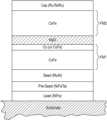
- FIG. 5is a schematic cross-sectional view of a FM1-layer/MgO/FM2-layer structure according to an embodiment of the invention with an improved seed layer and boron-free FM1 and FM2 layers.
- FIG. 6 Ais a schematic of a side view showing the growth of the FM1 and tunneling barrier layer with (001) texture on the B2 structure seed layer.
- FIG. 6 Bis a schematic top view of the (001) planes of the RuAl (seed), CoFe (FM1) and MgO (tunneling barrier) layers and shows the NaCl structure of the MgO layer with its (001) plane grown at a 45 degree angle on the CoFe layer.
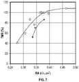
- FIG. 7is a graph of measured TMR vs. resistance-area product (RA) for a prior art dual free layer (DFL) device and a DFL device according to an embodiment of the invention.
- FIG. 1illustrates a cross-sectional view of two types of TMR read head 10 .
- the TMR read headincludes a bottom ferromagnetic (FM1) layer 18 , an insulating tunneling barrier layer 20 , and a top ferromagnetic (FM2) layer 32 .
- the TMR read headhas bottom and top nonmagnetic electrodes or leads 12 , 14 , respectively, with the bottom nonmagnetic electrode 12 being formed on a suitable substrate.
- a seed layer(not shown) can be located between the bottom lead and FM1, and a cap layer (not shown) can be located between FM2 and the top lead).
- both FM1 and FM2are “free” ferromagnetic layers because their magnetizations are free to rotate relative to one another with a scissoring effect in the presence of an external magnetic field from the recorded magnetic media.
- a pinned-type TMR deviceeither FM1 or FM2 has its magnetization fixed or pinned while the other ferromagnetic layer has its magnetization free to rotate in the presence of an external magnetic field.
- the pinned ferromagnetic layeris called the reference layer because its magnetization is prevented from rotation.
- the magnetization of the reference layercan be fixed or pinned by being formed of a high-coercivity film or by being exchange-coupled to an antiferromagnetic (AF) “pinning” layer.
- the pinned-type TMR devicecan be used as memory cells in a STT-MRAM device, as shown in FIG. 2 . A single MTJ is depicted in the STT-MRAM device.
- the orientation of the magnetization of the free ferromagnetic layercan be modified using a spin-polarized current to have an orientation either parallel or antiparallel to the fixed magnetization of the reference layer, thereby generating two resistance levels representing a 1 (parallel) or 0 (antiparallel) as a bit in the MTJ cell.
- the MTJcan similarly be used in an SOT-MRAM device, which primarily differs from the STT-MRAM in how writing is achieved through the SOT effect instead of the STT effect.
- a TMR devicecan also be part of a sensor device.
- the pinned-type TMR devicemay also be used as a read head in magnetic recording devices, like a hard disk drive, as shown in more detail in FIG. 3 .
- FIG. 3is a cross-sectional highly schematic view illustrating the structure of a prior-art pinned-type TMR read head like that used in a magnetic recording hard disk drive. This cross-sectional view is a view of what is commonly referred to as the gas-bearing surface (GBS) of the TMR read head.
- the TMR read headincludes a sensor stack of layers formed between two ferromagnetic shield layers S 1 , S 2 that are typically made of electroplated NiFe alloy films.
- the sensor stackincludes a ferromagnetic reference layer 120 having a pinned magnetization 121 oriented transversely (away from the page), a ferromagnetic free layer 110 having a magnetization 111 that can rotate in the plane of layer 110 in response to transverse external magnetic fields from a recording disk, and an electrically insulating tunneling barrier layer 130 , typically magnesium oxide (MgO), between the ferromagnetic reference layer 120 and ferromagnetic free layer 110 .
- MgOmagnesium oxide
- the reference layer 120may be a conventional “simple” or single pinned layer that has its magnetization direction 121 pinned or fixed, typically by being exchange coupled to an antiferromagnetic layer.
- the reference layer 120is part of the well-known antiparallel (AP) pinned or flux-closure structure, also called a “laminated” pinned layer, as described in U.S. Pat. No. 5,465,185.
- the AP-pinned structureminimizes magnetostatic coupling of the reference layer 120 with the free layer 110 .
- the AP-pinned structureincludes the reference ferromagnetic (AP2) layer 120 and a lower pinned ferromagnetic (AP1) layer 122 that are antiferromagnetically coupled across an AP coupling (APC) layer 123 , such as Ru, Ir, Rh, or Cr, or alloys thereof. Due to the antiparallel coupling across the APC layer 123 , the reference (AP2) and pinned (AP1) ferromagnetic layers 120 , 122 have their respective magnetizations 121 , 127 oriented antiparallel to each other.
- APIAP coupling
- the net magnetization of the AP2 and AP1 ferromagnetic layers 120 , 122is so small that a demagnetizing field induced by the flux closure structure in the ferromagnetic free layer 110 is substantially minimized, and thus it becomes feasible for the TMR read head to operate optimally.
- AFantiferromagnetic
- the seed layer 125facilitates the AF pinning layer 124 to grow a microstructure with a strong crystalline texture and thus develop strong antiferromagnetism.
- the AF pinning layer 124thus strongly exchange-couples to the ferromagnetic pinned layer 122 , and thereby rigidly pins the magnetization 127 of the ferromagnetic pinned layer 122 in a direction perpendicular to and away from the GBS.
- the antiparallel coupling across the APC layer 123then subsequently rigidly pins the magnetization 121 of the ferromagnetic reference layer 120 in a direction perpendicular to and towards the ABS, and antiparallel to magnetization 127 .
- the net magnetization of the ferromagnetic AP2 and AP1 layers 120 , 122is rigidly pinned, and thus the optimal operation of the TMR read head is ensured.
- a layer 112Located between the ferromagnetic free layer 110 and the upper shield layer S 2 is a layer 112 , sometimes called a capping or cap layer.
- the layer 112protects the ferromagnetic free layer 110 from chemical and mechanical damages during processing, so that ferromagnetic free layer 110 maintains good ferromagnetic properties.
- the magnetization 111 of the ferromagnetic free layer 110will rotate in responses to the magnetic fields.
- a sense current Isflows from the upper shield layer S 2 perpendicularly through the sensor stack to the lower shield layer S 1 , the magnetization rotation of the ferromagnetic free layer 111 will lead to the variation of the angle between the magnetizations of the ferromagnetic reference layer 120 and the ferromagnetic free layer 110 , which is detectable as the change in electrical resistance.
- the TMR read headis a current-perpendicular-to-the-plane (CPP) read head.
- CPPcurrent-perpendicular-to-the-plane
- FIG. 3also shows optional separate electrical leads 126 , 113 between shields S 1 , S 2 , respectively, and the sensor stack.
- the leadsare optional and may be used to adjust the shield-to-shield spacing. If the leads 126 and 113 are not present, the bottom and top shields S 1 and S 2 are used as electrical leads.
- the TMR read head shown in FIG. 3is a “bottom-pinned” read head because the AP-pinned structure is below the free layer 110 , the free layer 110 can be located below the AP-pinned structure. In such an arrangement the layers of the AP-pinned structure are reversed, with the AP2 layer 120 on top of and in contact with the barrier layer 130 .
- MgO tunnel junctionsare required to have (001) texture and perfect crystallinity.
- the MgO barrier layeris typically deposited as a NaCl (rock salt) crystalline structure with (001) texture on an amorphous layer by sputter deposition, and the subsequent annealing improves the crystalline structure by removing strain. It has been found that the use of a thin amorphous CoFeB or CoFeBTa layer in one or both ferromagnetic layers results in higher TMR or TMR ratio ( ⁇ R/R).
- the as-deposited amorphous CoFeB layeris known to promote the (001) textured MgO and higher TMR with CoFeB crystallization to (001) texture after annealing.
- FIG. 4is a schematic cross-sectional view of a typical FM1-layer/MgO/FM2-layer structure with boron present in both ferromagnetic layers.
- FM1 and FM2can both be free layers in a DFL device or one of FM1 and FM2 can be a reference layer in a pinned-type device.
- Each of the reference and free ferromagnetic layersis depicted as a thin (e.g., between about 1-4 ⁇ thick) CoFe “nanolayer” adjacent the MgO barrier layer, a CoFe layer and a CoFeB (and in some instances CoHf, CoFeBTa, or other amorphous insertion layer) layer between the nanolayer and the CoFe layer.
- the CoFeB layerhas a typical composition of (Co x Fe (100-x) ) (100-y) B y , where the subscripts represent atomic percent, x is between about 40 and 100, and y is between about 10 and 20.
- the total thickness of each of the FM1 and FM2 ferromagnetic layersis typically between about 20 and 80 ⁇ .
- Other materialsare well known for use in the ferromagnetic layers, such as Co or Fe nanolayers, NiFe alloys and Heusler alloys.
- FIG. 5is a schematic cross-sectional view of a FM1-layer/MgO/FM2-layer structure according to an embodiment of the invention with boron-free ferromagnetic layers and an improved seed layer.
- Each of the FM1 and FM2 layersmay be single layer or a multilayer.
- FM1is shown with an optional Co (or CoFe) nanolayer adjacent the MgO interface.
- An electrically conductive amorphous pre-seed layeris deposited directly on a lead layer formed on a suitable substrate.
- the pre-seed layermay be layer or multilayer comprising a material selected from a NiFeTa alloy, a CoFeTa alloy, a CoFeB alloy, a CoFeBTa alloy and Ta, with a total thickness in the range of about 5 to 50 ⁇ .
- the electrically conductive seed layerwhich is preferably a RuAl alloy (or alternatively a CrMo alloy) is deposited directly on the pre-seed layer and forms either as a B2 crystalline structure (also called a CsCl structure) in the case of RuAl or a BCC phase in the case of CrMo (Mo between about 30-50 atomic percent) with (001) texture, i.e., the (001) plane is parallel to the surfaces of the pre-seed layer and the substrate.
- the RuAl seed layerhas a thickness in the range of about 5 to 50 ⁇ and a preferred composition of Ru x Al (100-x) , where x is in atomic percent and is greater than or equal to 45 and less than or equal to 60.
- the boron-free FM1 layerwhich is preferably a CoFe alloy, is deposited on the seed layer, grows in the ⁇ 001> direction and inherits the (001) texture.
- An optional BCC sublayer(not shown in FIG. 5 ), like Cr, can be deposited on the seed layer prior to the deposition of the FM1 layer, in which case the FM1 layer is deposited directly on the sublayer.
- the phrase “on a layer”means there can be an intermediate layer or layers between an upper and lower layer, while the phrase “directly on a layer” means the upper layer is directly on and in contact with the lower layer).
- the boron-free FM1 layerhas a typical thickness in the range of 20 to 80 ⁇ and can also be a multilayer, as shown in FIG. 5 . While a CoFe alloy is the preferred material for FM1, other suitable materials with BCC structures that can inherit the (001) texture of the seed layer include a CoFeNi-based alloy, Heusler alloys like Co 2 MnSi, Co 2 MnAl, Co 2 MnGe, Co 2 FeSi and Co 2 FeAl, and half-Heusler alloys like NiMnSb.
- the MgO barrier layeris then deposited directly on the CoFe layer, or alternatively directly on the optional Co nanolayer (2 to 20 ⁇ ), to a thickness in the range of about 4 to 20 ⁇ .
- the MgO barrier layergrows epitaxially with the 001 texture on the FM1 layer. While MgO is preferred, other materials that can function as tunneling barrier layers and inherit the (001) texture of the FM1 layer include ZnO, MnO, CoO, TiO and VO, as well as spinel materials like MgAl 2 O 4 and MgGa 2 O 4 .
- FIG. 6 Ais a schematic of a side view showing the ⁇ 001> growth direction of the FM1 and tunneling barrier layer with (001) texture on RuAl seed layer.
- 6 Bis a schematic top view of the (001) planes of the RuAl (seed), CoFe (FM1) and MgO (tunneling barrier) layers and shows that the (001) plane of the NaCl structure of the MgO layer is at a 45 degree angle on the CoFe layer.
- the FM2 layeris then deposited on the MgO barrier layer. While the FM2 layer is also preferably a boron-free layer and preferably a CoFe alloy, it may contain B for soft magnetic properties or for lower magnetostriction.
- the FM2 layercan be a BCC structure or a multilayer that includes amorphous or FCC layers, provided the layer at the MgO interface has a BCC structure.
- the stackis annealed, preferably at about 180 to 280° C. for 2 to 5 hours. This improves the crystallinity of the FM1 and FM2 layers and the barrier layer by reducing strain. Unlike the prior art there is no boron diffusion into the barrier layer.
- a non-magnetic cap layerlike a Ru/Ta/Ru multilayer, may be formed on FM2.
- FIG. 7is a graph of measured TMR vs. RA for a prior art DFL wafer (like in FIG. 4 ) and a DFL wafer according to an embodiment of the invention (like in FIG. 5 ).
- the prior art DFL wafer whose data is shown by the lower curvehad a FM1 of a CoHf(20 ⁇ )/CoFeB(50 ⁇ )/Co(4 ⁇ ) multilayer and a FM2 of a CoFe(4 ⁇ )/CoFeB(50 ⁇ )/CoHf(20 ⁇ ) multilayer.
- the embodiment of the invention whose data is shown by the upper curvehad a RuAl seed layer, a FM1 of a CoFe(50 ⁇ )/Co(5 ⁇ ) multilayer and a FM2 of a CoFe(50 ⁇ ) layer.
- the embodiment of the inventionFor an RA range of about 0.34 to 0.38 (Ohm-micron 2 ) the embodiment of the invention has higher TMR between about 80-100%, compared to the prior art that has a range between about 50-85%. Similarly, for a TMR range of about 50-85%, the embodiment of the invention has lower RA between about 0.28 to 0.34 (Ohm-micron 2 ), compared to the prior art that has a range of about 0.34 to 0.38 (Ohm-micron 2 ).
Landscapes
- Hall/Mr Elements (AREA)
- Thin Magnetic Films (AREA)
- Mram Or Spin Memory Techniques (AREA)
Abstract
Description
- The invention relates generally to tunneling magnetoresistance (TMR) devices, and more particularly to a TMR device with a seed layer that improves formation of the tunneling barrier layer and performance of the TMR device.
- A tunneling magnetoresistance (TMR) device, also called a magnetic tunneling junction (MTJ) device, is comprised of two ferromagnetic layers separated by a thin insulating tunneling barrier layer. The barrier layer is typically made of a metallic oxide that is so sufficiently thin that quantum-mechanical tunneling of charge carriers occurs between the two ferromagnetic layers. While various metallic oxides, such as ZnO, MnO, CoO, TiO and VO, have been proposed as the tunneling barrier material, the most common material is crystalline magnesium oxide (MgO). The quantum-mechanical tunneling process is electron spin dependent, which means that an electrical resistance measured when applying a sense current across the junction depends on the spin-dependent electronic properties of the ferromagnetic and barrier layers and is a function of the relative orientation of the magnetizations of the two ferromagnetic layers.
- In one type of TMR or MTJ device, called a pinned-type, the magnetization of one of the ferromagnetic layers, called the reference layer, is fixed or pinned, while the magnetization of the other ferromagnetic layer, called the free layer, is free to rotate in response to external magnetic fields. Pinned-type TMR devices are usable in magnetic recording read heads, where the free ferromagnetic layer's magnetization rotates relative to the reference ferromagnetic layer's magnetization in the presence of a magnetic field from the recorded magnetic media. Pinned-type TMR devices are also usable in magnetic random access memory (MRAM) (e.g., spin transfer torque MRAM (STT-MRAM) and spin orbit torque MRAM (SOT-MRAM)) devices that use MTJs as memory storage bits or cells, where the magnetization of the free layer relative to the reference layer in the MTJ is changed directly with an electrical current. A TMR device can also be used as part of a magnetic sensor device usable in a variety of applications (e.g., industrial, automotive, medical).
- In another type of TMR device, called a dual free layer (DFL) type, there are two free ferromagnetic layers in which the magnetizations of both ferromagnetic layers are free to rotate relative to one another in a “scissoring” effect in response to an external magnetic field. DFL read heads for magnetic recording devices are described in U.S. Pat. No. 7,035,062 B2 and U.S. Pat. No. 8,670,217 B1.
- TMR devices with MgO tunneling barrier layers, like CoFe/MgO/CoFe tunnel junctions, exhibit a very large tunneling magnetoresistance (TMR) due to coherent tunneling of the electrons of certain symmetry. However, the ferromagnetic layers and MgO barrier layer are required to have perfect crystallinity to achieve the high TMR. The ferromagnetic layers and MgO barrier layer are typically formed by sputter deposition and subsequent annealing, which forms the crystalline structure. CoFe/MgO/CoFe tunnel junctions that exhibit the required low resistance-area product (RA) do not exhibit high TMR, likely due to inferior crystallinity of the MgO barrier layer. However, it has been found that when boron (B) is used in one or more of the ferromagnetic layers, such as using a thin amorphous CoFeB or CoFeBTa layer in a multilayer structure, higher TMR is observed after annealing. The amorphous CoFeB layer promotes better growth of the MgO with (001) texture (the surface plane parallel to the surface of the substrate), and thus higher TMR.
- Advanced TMR devices with even higher TMR will require a reduction in the resistance-area product (RA), which means that the MgO barrier layers will need to be made thinner. However, as the MgO thickness decreases the breakdown voltage and TMR also decrease, which is believed due, in part, to diffusion of boron into the MgO barrier layer. What is needed is a TMR device with a thin MgO barrier layer and thus reduced RA, but with high TMR.
- Embodiments of this invention relate to a TMR device with an improved seed layer for the lower or first ferromagnetic layer that eliminates the need for boron in the ferromagnetic layers. The seed layer, for example a RuAl alloy, has a B2 crystalline structure (also called a CsCl crystalline structure) with (001) texture, meaning that the (001) plane is parallel to the surface of the TMR device substrate. The subsequently deposited first ferromagnetic layer, like a CoFe alloy, and the tunneling barrier layer, typically MgO, also inherit the (001) texture of the seed layer. After deposition of the second ferromagnetic layer and annealing, the crystallization of the ferromagnetic layers and tunnel barrier layer is improved, due to the absence of diffused boron and the larger grain size of the boron-free ferromagnetic layers, which reduces defects at the grain boundaries. The resulting TMR device has reduced RA and increased TMR over the prior art boron-containing TMR device.
- For a fuller understanding of the nature and advantages of the present invention, reference should be made to the following detailed description taken together with the accompanying figures.
FIG.1 is a cross-sectional view illustrating the structure of two types of conventional tunneling magnetoresistance (TMR) devices.FIG.2 is perspective view of a magnetic tunnel junction (MTJ) as a memory cell in a spin transfer torque magnetic random access memory (STT-MRAM) device.FIG.3 is a cross-sectional view illustrating the detailed structure of a prior-art pinned-type TMR read head.FIG.4 is a schematic illustrating a typical FM1-layer/MgO/FM2-layer structure with boron present in both ferromagnetic (FM) layers.FIG.5 is a schematic cross-sectional view of a FM1-layer/MgO/FM2-layer structure according to an embodiment of the invention with an improved seed layer and boron-free FM1 and FM2 layers.FIG.6A is a schematic of a side view showing the growth of the FM1 and tunneling barrier layer with (001) texture on the B2 structure seed layer.FIG.6B is a schematic top view of the (001) planes of the RuAl (seed), CoFe (FM1) and MgO (tunneling barrier) layers and shows the NaCl structure of the MgO layer with its (001) plane grown at a 45 degree angle on the CoFe layer.FIG.7 is a graph of measured TMR vs. resistance-area product (RA) for a prior art dual free layer (DFL) device and a DFL device according to an embodiment of the invention.FIG.1 illustrates a cross-sectional view of two types of TMR read head10. The TMR read head includes a bottom ferromagnetic (FM1)layer 18, an insulatingtunneling barrier layer 20, and a top ferromagnetic (FM2)layer 32. The TMR read head has bottom and top nonmagnetic electrodes or leads12,14, respectively, with the bottomnonmagnetic electrode 12 being formed on a suitable substrate. A seed layer (not shown) can be located between the bottom lead and FM1, and a cap layer (not shown) can be located between FM2 and the top lead). In a DFL read head, both FM1 and FM2 are “free” ferromagnetic layers because their magnetizations are free to rotate relative to one another with a scissoring effect in the presence of an external magnetic field from the recorded magnetic media.- In a pinned-type TMR device either FM1 or FM2 has its magnetization fixed or pinned while the other ferromagnetic layer has its magnetization free to rotate in the presence of an external magnetic field. The pinned ferromagnetic layer is called the reference layer because its magnetization is prevented from rotation. The magnetization of the reference layer can be fixed or pinned by being formed of a high-coercivity film or by being exchange-coupled to an antiferromagnetic (AF) “pinning” layer. The pinned-type TMR device can be used as memory cells in a STT-MRAM device, as shown in
FIG.2 . A single MTJ is depicted in the STT-MRAM device. The orientation of the magnetization of the free ferromagnetic layer can be modified using a spin-polarized current to have an orientation either parallel or antiparallel to the fixed magnetization of the reference layer, thereby generating two resistance levels representing a 1 (parallel) or 0 (antiparallel) as a bit in the MTJ cell. The MTJ can similarly be used in an SOT-MRAM device, which primarily differs from the STT-MRAM in how writing is achieved through the SOT effect instead of the STT effect. As noted above, besides read head and magnetic memory applications, a TMR device can also be part of a sensor device. - The pinned-type TMR device may also be used as a read head in magnetic recording devices, like a hard disk drive, as shown in more detail in
FIG.3 .FIG.3 is a cross-sectional highly schematic view illustrating the structure of a prior-art pinned-type TMR read head like that used in a magnetic recording hard disk drive. This cross-sectional view is a view of what is commonly referred to as the gas-bearing surface (GBS) of the TMR read head. The TMR read head includes a sensor stack of layers formed between two ferromagnetic shield layers S1, S2 that are typically made of electroplated NiFe alloy films. The sensor stack includes aferromagnetic reference layer 120 having apinned magnetization 121 oriented transversely (away from the page), a ferromagneticfree layer 110 having a magnetization111 that can rotate in the plane oflayer 110 in response to transverse external magnetic fields from a recording disk, and an electrically insulatingtunneling barrier layer 130, typically magnesium oxide (MgO), between theferromagnetic reference layer 120 and ferromagneticfree layer 110. - The
reference layer 120 may be a conventional “simple” or single pinned layer that has itsmagnetization direction 121 pinned or fixed, typically by being exchange coupled to an antiferromagnetic layer. However, in the example ofFIG.3 , thereference layer 120 is part of the well-known antiparallel (AP) pinned or flux-closure structure, also called a “laminated” pinned layer, as described in U.S. Pat. No. 5,465,185. The AP-pinned structure minimizes magnetostatic coupling of thereference layer 120 with thefree layer 110. The AP-pinned structure includes the reference ferromagnetic (AP2)layer 120 and a lower pinned ferromagnetic (AP1)layer 122 that are antiferromagnetically coupled across an AP coupling (APC)layer 123, such as Ru, Ir, Rh, or Cr, or alloys thereof. Due to the antiparallel coupling across theAPC layer 123, the reference (AP2) and pinned (AP1)ferromagnetic layers respective magnetizations ferromagnetic layers free layer 110 is substantially minimized, and thus it becomes feasible for the TMR read head to operate optimally. - Located between the substrate, lower shield layer S1, and the AP-pinned structure are
seed layer 125 and an antiferromagnetic (AF) pinninglayer 124. Theseed layer 125 facilitates theAF pinning layer 124 to grow a microstructure with a strong crystalline texture and thus develop strong antiferromagnetism. TheAF pinning layer 124 thus strongly exchange-couples to the ferromagnetic pinnedlayer 122, and thereby rigidly pins themagnetization 127 of the ferromagnetic pinnedlayer 122 in a direction perpendicular to and away from the GBS. The antiparallel coupling across theAPC layer 123 then subsequently rigidly pins themagnetization 121 of theferromagnetic reference layer 120 in a direction perpendicular to and towards the ABS, and antiparallel tomagnetization 127. As a result, the net magnetization of the ferromagnetic AP2 andAP1 layers - Located between the ferromagnetic
free layer 110 and the upper shield layer S2 is alayer 112, sometimes called a capping or cap layer. Thelayer 112 protects the ferromagneticfree layer 110 from chemical and mechanical damages during processing, so that ferromagneticfree layer 110 maintains good ferromagnetic properties. - In the presence of external magnetic fields in the range of interest, i.e., magnetic fields from written data on the recording disk, while the net magnetization of the
ferromagnetic layers free layer 110 will rotate in responses to the magnetic fields. Thus, when a sense current Is flows from the upper shield layer S2 perpendicularly through the sensor stack to the lower shield layer S1, the magnetization rotation of the ferromagnetic free layer111 will lead to the variation of the angle between the magnetizations of theferromagnetic reference layer 120 and the ferromagneticfree layer 110, which is detectable as the change in electrical resistance. Because the sense current is directed perpendicularly through the stack of layers between the two shields S1 and S2, the TMR read head is a current-perpendicular-to-the-plane (CPP) read head. FIG.3 also shows optional separateelectrical leads FIG.3 is a “bottom-pinned” read head because the AP-pinned structure is below thefree layer 110, thefree layer 110 can be located below the AP-pinned structure. In such an arrangement the layers of the AP-pinned structure are reversed, with theAP2 layer 120 on top of and in contact with thebarrier layer 130.- MgO tunnel junctions are required to have (001) texture and perfect crystallinity. The MgO barrier layer is typically deposited as a NaCl (rock salt) crystalline structure with (001) texture on an amorphous layer by sputter deposition, and the subsequent annealing improves the crystalline structure by removing strain. It has been found that the use of a thin amorphous CoFeB or CoFeBTa layer in one or both ferromagnetic layers results in higher TMR or TMR ratio (ΔR/R). The as-deposited amorphous CoFeB layer is known to promote the (001) textured MgO and higher TMR with CoFeB crystallization to (001) texture after annealing.
FIG.4 is a schematic cross-sectional view of a typical FM1-layer/MgO/FM2-layer structure with boron present in both ferromagnetic layers. FM1 and FM2 can both be free layers in a DFL device or one of FM1 and FM2 can be a reference layer in a pinned-type device. Each of the reference and free ferromagnetic layers is depicted as a thin (e.g., between about 1-4 Å thick) CoFe “nanolayer” adjacent the MgO barrier layer, a CoFe layer and a CoFeB (and in some instances CoHf, CoFeBTa, or other amorphous insertion layer) layer between the nanolayer and the CoFe layer. The CoFeB layer has a typical composition of (CoxFe(100-x))(100-y)By, where the subscripts represent atomic percent, x is between about 40 and 100, and y is between about 10 and 20. The total thickness of each of the FM1 and FM2 ferromagnetic layers is typically between about 20 and 80 Å. Other materials are well known for use in the ferromagnetic layers, such as Co or Fe nanolayers, NiFe alloys and Heusler alloys.- However, it has been discovered that in the prior art TMR device of
FIG.4 boron diffuses into the MgO barrier layer during annealing, which decreases the breakdown voltage and TMR. Also, for advanced TMR devices the MgO needs to be made thinner to reduce the resistance-area product (RA). Thinner MgO barrier layers would be even more susceptible to boron diffusion. Also, the smaller grains of the MgO deposited on the CoFeB means that there can be more defects in the MgO grain boundaries after annealing. FIG.5 is a schematic cross-sectional view of a FM1-layer/MgO/FM2-layer structure according to an embodiment of the invention with boron-free ferromagnetic layers and an improved seed layer. Each of the FM1 and FM2 layers may be single layer or a multilayer. FM1 is shown with an optional Co (or CoFe) nanolayer adjacent the MgO interface. An electrically conductive amorphous pre-seed layer is deposited directly on a lead layer formed on a suitable substrate. The pre-seed layer may be layer or multilayer comprising a material selected from a NiFeTa alloy, a CoFeTa alloy, a CoFeB alloy, a CoFeBTa alloy and Ta, with a total thickness in the range of about 5 to 50 Å. The electrically conductive seed layer, which is preferably a RuAl alloy (or alternatively a CrMo alloy) is deposited directly on the pre-seed layer and forms either as a B2 crystalline structure (also called a CsCl structure) in the case of RuAl or a BCC phase in the case of CrMo (Mo between about 30-50 atomic percent) with (001) texture, i.e., the (001) plane is parallel to the surfaces of the pre-seed layer and the substrate. The RuAl seed layer has a thickness in the range of about 5 to 50 Å and a preferred composition of RuxAl(100-x), where x is in atomic percent and is greater than or equal to 45 and less than or equal to 60. The boron-free FM1 layer, which is preferably a CoFe alloy, is deposited on the seed layer, grows in the <001> direction and inherits the (001) texture. An optional BCC sublayer (not shown inFIG.5 ), like Cr, can be deposited on the seed layer prior to the deposition of the FM1 layer, in which case the FM1 layer is deposited directly on the sublayer. (As used herein, the phrase “on a layer” means there can be an intermediate layer or layers between an upper and lower layer, while the phrase “directly on a layer” means the upper layer is directly on and in contact with the lower layer). The boron-free FM1 layer has a typical thickness in the range of 20 to 80 Å and can also be a multilayer, as shown inFIG.5 . While a CoFe alloy is the preferred material for FM1, other suitable materials with BCC structures that can inherit the (001) texture of the seed layer include a CoFeNi-based alloy, Heusler alloys like Co2MnSi, Co2MnAl, Co2MnGe, Co2FeSi and Co2FeAl, and half-Heusler alloys like NiMnSb. The MgO barrier layer is then deposited directly on the CoFe layer, or alternatively directly on the optional Co nanolayer (2 to 20 Å), to a thickness in the range of about 4 to 20 Å. The MgO barrier layer grows epitaxially with the 001 texture on the FM1 layer. While MgO is preferred, other materials that can function as tunneling barrier layers and inherit the (001) texture of the FM1 layer include ZnO, MnO, CoO, TiO and VO, as well as spinel materials like MgAl2O4and MgGa2O4.FIG.6A is a schematic of a side view showing the <001> growth direction of the FM1 and tunneling barrier layer with (001) texture on RuAl seed layer.FIG.6B is a schematic top view of the (001) planes of the RuAl (seed), CoFe (FM1) and MgO (tunneling barrier) layers and shows that the (001) plane of the NaCl structure of the MgO layer is at a 45 degree angle on the CoFe layer.- The FM2 layer is then deposited on the MgO barrier layer. While the FM2 layer is also preferably a boron-free layer and preferably a CoFe alloy, it may contain B for soft magnetic properties or for lower magnetostriction. The FM2 layer can be a BCC structure or a multilayer that includes amorphous or FCC layers, provided the layer at the MgO interface has a BCC structure. After deposition of the layers in the stack, the stack is annealed, preferably at about 180 to 280° C. for 2 to 5 hours. This improves the crystallinity of the FM1 and FM2 layers and the barrier layer by reducing strain. Unlike the prior art there is no boron diffusion into the barrier layer. Also, defects in the crystalline structure of the barrier layer, which is typically MgO, are at the grain boundaries, but because the grains in the barrier layer in various embodiments of this invention are larger than the grains of the barrier layer formed on the CoFeB layer of the prior art, there are fewer defects in the barrier layer after annealing. A non-magnetic cap layer, like a Ru/Ta/Ru multilayer, may be formed on FM2.
FIG.7 is a graph of measured TMR vs. RA for a prior art DFL wafer (like inFIG.4 ) and a DFL wafer according to an embodiment of the invention (like inFIG.5 ). The TMR ratio is given by ΔR/R=(RAP−RP)/RP, where RPand RAPrepresent the resistance measured for parallel and antiparallel configurations of the ferromagnetic layer magnetizations. The prior art DFL wafer whose data is shown by the lower curve had a FM1 of a CoHf(20 Å)/CoFeB(50 Å)/Co(4 Å) multilayer and a FM2 of a CoFe(4 Å)/CoFeB(50 Å)/CoHf(20 Å) multilayer. The embodiment of the invention whose data is shown by the upper curve had a RuAl seed layer, a FM1 of a CoFe(50 Å)/Co(5 Å) multilayer and a FM2 of a CoFe(50 Å) layer. For an RA range of about 0.34 to 0.38 (Ohm-micron2) the embodiment of the invention has higher TMR between about 80-100%, compared to the prior art that has a range between about 50-85%. Similarly, for a TMR range of about 50-85%, the embodiment of the invention has lower RA between about 0.28 to 0.34 (Ohm-micron2), compared to the prior art that has a range of about 0.34 to 0.38 (Ohm-micron2).- While the present invention has been particularly shown and described with reference to the preferred embodiments, it will be understood by those skilled in the art that various changes in form and detail may be made without departing from the spirit and scope of the invention. Accordingly, the disclosed invention is to be considered merely as illustrative and limited in scope only as specified in the appended claims.
Claims (25)
Priority Applications (4)
| Application Number | Priority Date | Filing Date | Title |
|---|---|---|---|
| US17/472,019US12035634B2 (en) | 2021-09-10 | 2021-09-10 | Tunneling magnetoresistive (TMR) device with improved seed layer |
| CN202280049425.4ACN117730640A (en) | 2021-09-10 | 2022-05-08 | Tunneling magneto-resistance (TMR) device with improved seed layer |
| JP2024502156AJP7731495B2 (en) | 2021-09-10 | 2022-05-08 | Tunneling magnetoresistance (TMR) device with improved seed layer |
| PCT/US2022/028238WO2023038680A1 (en) | 2021-09-10 | 2022-05-08 | Tunneling magnetoresistive (tmr) device with improved seed layer |
Applications Claiming Priority (1)
| Application Number | Priority Date | Filing Date | Title |
|---|---|---|---|
| US17/472,019US12035634B2 (en) | 2021-09-10 | 2021-09-10 | Tunneling magnetoresistive (TMR) device with improved seed layer |
Publications (2)
| Publication Number | Publication Date |
|---|---|
| US20230084970A1true US20230084970A1 (en) | 2023-03-16 |
| US12035634B2 US12035634B2 (en) | 2024-07-09 |
Family
ID=85478752
Family Applications (1)
| Application Number | Title | Priority Date | Filing Date |
|---|---|---|---|
| US17/472,019Active2042-10-21US12035634B2 (en) | 2021-09-10 | 2021-09-10 | Tunneling magnetoresistive (TMR) device with improved seed layer |
Country Status (4)
| Country | Link |
|---|---|
| US (1) | US12035634B2 (en) |
| JP (1) | JP7731495B2 (en) |
| CN (1) | CN117730640A (en) |
| WO (1) | WO2023038680A1 (en) |
Cited By (2)
| Publication number | Priority date | Publication date | Assignee | Title |
|---|---|---|---|---|
| US20240107893A1 (en)* | 2022-09-23 | 2024-03-28 | Western Digital Technologies, Inc. | Magnetoresistive Devices Comprising A Synthetic Antiferromagnetic Coupling Layer Of RuAl Having a (110) Texture |
| US12040114B2 (en) | 2022-09-14 | 2024-07-16 | Western Digital Technologies, Inc. | Magnetoresistive device comprising a synthetic antiferromagnetic coupling layer of RuAl having a (001) texture |
Citations (8)
| Publication number | Priority date | Publication date | Assignee | Title |
|---|---|---|---|---|
| US20060218773A1 (en)* | 2005-03-31 | 2006-10-05 | Hitachi Global Storage Technologies | Method for manufacturing a magnetic read sensor employing oblique etched underlayers for inducing uniaxial magnetic anisotropy in a hard magnetic in-stack bias layer |
| US20070015293A1 (en)* | 2005-07-14 | 2007-01-18 | Headway Technologies, Inc. | TMR device with surfactant layer on top of CoFexBy/CoFez inner pinned layer |
| US20070111332A1 (en)* | 2005-11-16 | 2007-05-17 | Headway Technologies, Inc. | Low resistance tunneling magnetoresistive sensor with natural oxidized double MgO barrier |
| US20090257151A1 (en)* | 2008-03-27 | 2009-10-15 | Tdk Corporation & Kabushiki Kaisha Toshiba | Thin seeded Co/Ni multilayer film with perpendicular anisotropy for spintronic device applications |
| US20130015539A1 (en)* | 2011-07-13 | 2013-01-17 | Won Joon Choi | Magnetic memory device having increased margin in thickness of magnetic layers |
| US20130107616A1 (en)* | 2010-07-09 | 2013-05-02 | Hideo Ohno | Magnetoresistive effect element and random access memory using same |
| US9099124B1 (en)* | 2014-09-28 | 2015-08-04 | HGST Netherlands B.V. | Tunneling magnetoresistive (TMR) device with MgO tunneling barrier layer and nitrogen-containing layer for minimization of boron diffusion |
| US20170213957A1 (en)* | 2014-05-27 | 2017-07-27 | Industry-University Cooperation Foundation Hanyang University | Magnetic tunnel junction element and manufacturing method therefor |
Family Cites Families (13)
| Publication number | Priority date | Publication date | Assignee | Title |
|---|---|---|---|---|
| US6846543B2 (en) | 1999-04-20 | 2005-01-25 | Hitachi Global Storage Technologies Netherlands, B.V. | Thin film magnetic recording disk with ruthenium-aluminum layer |
| US7035062B1 (en) | 2001-11-29 | 2006-04-25 | Seagate Technology Llc | Structure to achieve sensitivity and linear density in tunneling GMR heads using orthogonal magnetic alignments |
| US6872478B2 (en) | 2003-06-26 | 2005-03-29 | Hitachi Global Storage Technologies Netherlands, B.V. | Magnetic thin film media with a pre-seed layer of CrTiAl |
| EP1737055B1 (en) | 2004-03-12 | 2012-01-11 | Japan Science and Technology Agency | Magnetoresistive element and its manufacturing method |
| US7859034B2 (en) | 2005-09-20 | 2010-12-28 | Grandis Inc. | Magnetic devices having oxide antiferromagnetic layer next to free ferromagnetic layer |
| JP2010212631A (en)* | 2009-03-12 | 2010-09-24 | Fujitsu Ltd | Magnetoresistance effect element, and magnetic memory device |
| JP2011108320A (en)* | 2009-11-17 | 2011-06-02 | Hitachi Global Storage Technologies Netherlands Bv | Magnetic head and method for manufacturing the same |
| US8564080B2 (en)* | 2010-07-16 | 2013-10-22 | Qualcomm Incorporated | Magnetic storage element utilizing improved pinned layer stack |
| US20120299132A1 (en) | 2011-05-27 | 2012-11-29 | Hitachi Global Storage Technologies Netherlands B.V. | Tunneling magnetoresistance (tmr) read sensor with low-contact-resistance interfaces |
| US20130001717A1 (en)* | 2011-07-01 | 2013-01-03 | Yuchen Zhou | Perpendicular mram with mtj including laminated magnetic layers |
| US8670217B1 (en) | 2013-02-11 | 2014-03-11 | HGST Netherlands B.V. | Scissoring-type current-perpendicular-to-the-plane (CPP) magnetoresistive sensor with free layers having shape anisotropy |
| JP6411186B2 (en)* | 2014-11-19 | 2018-10-24 | 株式会社東芝 | Magnetoresistive element and magnetic memory |
| KR102397904B1 (en) | 2015-09-17 | 2022-05-13 | 삼성전자주식회사 | Free Layer Having a Low Boron Concentration Region and a High Boron Concentration Region, Magneto-resistive Cell, and Magneto-resistive Random Access Memory Device Having the Same, and Methods of Fabricating the Same |
- 2021
- 2021-09-10USUS17/472,019patent/US12035634B2/enactiveActive
- 2022
- 2022-05-08WOPCT/US2022/028238patent/WO2023038680A1/ennot_activeCeased
- 2022-05-08CNCN202280049425.4Apatent/CN117730640A/enactivePending
- 2022-05-08JPJP2024502156Apatent/JP7731495B2/enactiveActive
Patent Citations (8)
| Publication number | Priority date | Publication date | Assignee | Title |
|---|---|---|---|---|
| US20060218773A1 (en)* | 2005-03-31 | 2006-10-05 | Hitachi Global Storage Technologies | Method for manufacturing a magnetic read sensor employing oblique etched underlayers for inducing uniaxial magnetic anisotropy in a hard magnetic in-stack bias layer |
| US20070015293A1 (en)* | 2005-07-14 | 2007-01-18 | Headway Technologies, Inc. | TMR device with surfactant layer on top of CoFexBy/CoFez inner pinned layer |
| US20070111332A1 (en)* | 2005-11-16 | 2007-05-17 | Headway Technologies, Inc. | Low resistance tunneling magnetoresistive sensor with natural oxidized double MgO barrier |
| US20090257151A1 (en)* | 2008-03-27 | 2009-10-15 | Tdk Corporation & Kabushiki Kaisha Toshiba | Thin seeded Co/Ni multilayer film with perpendicular anisotropy for spintronic device applications |
| US20130107616A1 (en)* | 2010-07-09 | 2013-05-02 | Hideo Ohno | Magnetoresistive effect element and random access memory using same |
| US20130015539A1 (en)* | 2011-07-13 | 2013-01-17 | Won Joon Choi | Magnetic memory device having increased margin in thickness of magnetic layers |
| US20170213957A1 (en)* | 2014-05-27 | 2017-07-27 | Industry-University Cooperation Foundation Hanyang University | Magnetic tunnel junction element and manufacturing method therefor |
| US9099124B1 (en)* | 2014-09-28 | 2015-08-04 | HGST Netherlands B.V. | Tunneling magnetoresistive (TMR) device with MgO tunneling barrier layer and nitrogen-containing layer for minimization of boron diffusion |
Cited By (3)
| Publication number | Priority date | Publication date | Assignee | Title |
|---|---|---|---|---|
| US12040114B2 (en) | 2022-09-14 | 2024-07-16 | Western Digital Technologies, Inc. | Magnetoresistive device comprising a synthetic antiferromagnetic coupling layer of RuAl having a (001) texture |
| US20240107893A1 (en)* | 2022-09-23 | 2024-03-28 | Western Digital Technologies, Inc. | Magnetoresistive Devices Comprising A Synthetic Antiferromagnetic Coupling Layer Of RuAl Having a (110) Texture |
| US12207563B2 (en)* | 2022-09-23 | 2025-01-21 | Western Digital Technologies, Inc. | Magnetoresistive devices comprising a synthetic antiferromagnetic coupling layer of RuAl having a (110) texture |
Also Published As
| Publication number | Publication date |
|---|---|
| CN117730640A (en) | 2024-03-19 |
| US12035634B2 (en) | 2024-07-09 |
| JP2024526786A (en) | 2024-07-19 |
| JP7731495B2 (en) | 2025-08-29 |
| WO2023038680A1 (en) | 2023-03-16 |
Similar Documents
| Publication | Publication Date | Title |
|---|---|---|
| US9099124B1 (en) | Tunneling magnetoresistive (TMR) device with MgO tunneling barrier layer and nitrogen-containing layer for minimization of boron diffusion | |
| US9177573B1 (en) | Tunneling magnetoresistive (TMR) device with magnesium oxide tunneling barrier layer and free layer having insertion layer | |
| US7443639B2 (en) | Magnetic tunnel junctions including crystalline and amorphous tunnel barrier materials | |
| US6977801B2 (en) | Magnetoresistive device with exchange-coupled structure having half-metallic ferromagnetic Heusler alloy in the pinned layer | |
| US8385026B2 (en) | Tunneling magnetoresistive (TMR) read head with low magnetic noise | |
| US7300711B2 (en) | Magnetic tunnel junctions with high tunneling magnetoresistance using non-bcc magnetic materials | |
| US7357995B2 (en) | Magnetic tunnel barriers and associated magnetic tunnel junctions with high tunneling magnetoresistance | |
| US7098495B2 (en) | Magnetic tunnel junction element structures and methods for fabricating the same | |
| US7349187B2 (en) | Tunnel barriers based on alkaline earth oxides | |
| US8154829B2 (en) | Tunneling magnetoresistive (TMR) device with improved ferromagnetic underlayer for MgO tunneling barrier layer | |
| US20070063237A1 (en) | Magnetic device having multilayered free ferromagnetic layer | |
| US20100244163A1 (en) | Magnetoresistive element and magnetic memory | |
| US20080198514A1 (en) | Magnetoresistive device, magnetic head, magnetic storage apparatus, and magnetic memory | |
| KR101584747B1 (en) | Magnetic memory element | |
| US20060012926A1 (en) | Magnetic tunnel barriers and associated magnetic tunnel junctions with high tunneling magnetoresistance | |
| US12035634B2 (en) | Tunneling magnetoresistive (TMR) device with improved seed layer | |
| US20080241596A1 (en) | Magnetoresistive Multilayer Film | |
| US8091209B1 (en) | Magnetic sensing device including a sense enhancing layer | |
| US20230276714A1 (en) | Semiconductor device and method of making the same | |
| US20210318394A1 (en) | Magnetoresistance effect element |
Legal Events
| Date | Code | Title | Description |
|---|---|---|---|
| AS | Assignment | Owner name:WESTERN DIGITAL TECHNOLOGIES, INC., UNITED STATES Free format text:ASSIGNMENT OF ASSIGNORS INTEREST;ASSIGNORS:OKAMURA, SUSUMU;KAISER, CHRISTIAN;YORK, BRIAN R;SIGNING DATES FROM 20210908 TO 20210910;REEL/FRAME:057449/0926 | |
| FEPP | Fee payment procedure | Free format text:ENTITY STATUS SET TO UNDISCOUNTED (ORIGINAL EVENT CODE: BIG.); ENTITY STATUS OF PATENT OWNER: LARGE ENTITY | |
| STPP | Information on status: patent application and granting procedure in general | Free format text:DOCKETED NEW CASE - READY FOR EXAMINATION | |
| AS | Assignment | Owner name:JPMORGAN CHASE BANK, N.A., AS AGENT, ILLINOIS Free format text:SECURITY INTEREST;ASSIGNOR:WESTERN DIGITAL TECHNOLOGIES, INC.;REEL/FRAME:058426/0815 Effective date:20211104 | |
| AS | Assignment | Owner name:WESTERN DIGITAL TECHNOLOGIES, INC., CALIFORNIA Free format text:RELEASE OF SECURITY INTEREST AT REEL 058426 FRAME 0815;ASSIGNOR:JPMORGAN CHASE BANK, N.A.;REEL/FRAME:058965/0679 Effective date:20220203 | |
| AS | Assignment | Owner name:JPMORGAN CHASE BANK, N.A., ILLINOIS Free format text:PATENT COLLATERAL AGREEMENT - A&R LOAN AGREEMENT;ASSIGNOR:WESTERN DIGITAL TECHNOLOGIES, INC.;REEL/FRAME:064715/0001 Effective date:20230818 Owner name:JPMORGAN CHASE BANK, N.A., ILLINOIS Free format text:PATENT COLLATERAL AGREEMENT - DDTL LOAN AGREEMENT;ASSIGNOR:WESTERN DIGITAL TECHNOLOGIES, INC.;REEL/FRAME:067045/0156 Effective date:20230818 | |
| STPP | Information on status: patent application and granting procedure in general | Free format text:NON FINAL ACTION MAILED | |
| STPP | Information on status: patent application and granting procedure in general | Free format text:RESPONSE TO NON-FINAL OFFICE ACTION ENTERED AND FORWARDED TO EXAMINER | |
| STPP | Information on status: patent application and granting procedure in general | Free format text:NOTICE OF ALLOWANCE MAILED -- APPLICATION RECEIVED IN OFFICE OF PUBLICATIONS | |
| STPP | Information on status: patent application and granting procedure in general | Free format text:PUBLICATIONS -- ISSUE FEE PAYMENT VERIFIED | |
| STCF | Information on status: patent grant | Free format text:PATENTED CASE |