US20230070943A1 - Beam Deflector Metasurface - Google Patents
Beam Deflector MetasurfaceDownload PDFInfo
- Publication number
- US20230070943A1 US20230070943A1US17/466,813US202117466813AUS2023070943A1US 20230070943 A1US20230070943 A1US 20230070943A1US 202117466813 AUS202117466813 AUS 202117466813AUS 2023070943 A1US2023070943 A1US 2023070943A1
- Authority
- US
- United States
- Prior art keywords
- pillars
- metasurface
- beam deflector
- deflectors
- concentric
- Prior art date
- Legal status (The legal status is an assumption and is not a legal conclusion. Google has not performed a legal analysis and makes no representation as to the accuracy of the status listed.)
- Granted
Links
- 230000010287polarizationEffects0.000claimsabstractdescription7
- 230000035945sensitivityEffects0.000claimsabstractdescription3
- 238000000034methodMethods0.000claimsdescription20
- 239000000758substrateSubstances0.000claimsdescription19
- 238000006880cross-coupling reactionMethods0.000abstractdescription5
- 238000003384imaging methodMethods0.000abstractdescription5
- 230000008901benefitEffects0.000abstractdescription3
- 238000012545processingMethods0.000abstractdescription2
- 230000006866deteriorationEffects0.000abstract1
- 238000000059patterningMethods0.000abstract1
- 230000003287optical effectEffects0.000description19
- 239000011295pitchSubstances0.000description11
- 238000013461designMethods0.000description8
- 230000008569processEffects0.000description6
- 239000002086nanomaterialSubstances0.000description5
- 230000008859changeEffects0.000description4
- 230000004048modificationEffects0.000description4
- 238000012986modificationMethods0.000description4
- 238000009826distributionMethods0.000description3
- 239000000463materialSubstances0.000description3
- 230000000737periodic effectEffects0.000description3
- 230000002542deteriorative effectEffects0.000description2
- 230000010363phase shiftEffects0.000description2
- 230000004044responseEffects0.000description2
- 238000009827uniform distributionMethods0.000description2
- 238000013316zoningMethods0.000description2
- 230000003667anti-reflective effectEffects0.000description1
- 230000009286beneficial effectEffects0.000description1
- 230000001419dependent effectEffects0.000description1
- 238000001514detection methodMethods0.000description1
- 238000005516engineering processMethods0.000description1
- 230000007717exclusionEffects0.000description1
- 230000010354integrationEffects0.000description1
- 239000007788liquidSubstances0.000description1
- 238000004519manufacturing processMethods0.000description1
- 239000000178monomerSubstances0.000description1
- 239000002105nanoparticleSubstances0.000description1
- 238000009828non-uniform distributionMethods0.000description1
- 230000000704physical effectEffects0.000description1
- 230000001902propagating effectEffects0.000description1
- 238000000926separation methodMethods0.000description1
- 238000007493shaping processMethods0.000description1
- 230000008685targetingEffects0.000description1
- 238000012546transferMethods0.000description1
Images


Classifications
- G—PHYSICS
- G02—OPTICS
- G02B—OPTICAL ELEMENTS, SYSTEMS OR APPARATUS
- G02B1/00—Optical elements characterised by the material of which they are made; Optical coatings for optical elements
- G02B1/002—Optical elements characterised by the material of which they are made; Optical coatings for optical elements made of materials engineered to provide properties not available in nature, e.g. metamaterials
- G—PHYSICS
- G02—OPTICS
- G02B—OPTICAL ELEMENTS, SYSTEMS OR APPARATUS
- G02B3/00—Simple or compound lenses
- G02B3/0006—Arrays
- G02B3/0037—Arrays characterized by the distribution or form of lenses
- G02B3/0043—Inhomogeneous or irregular arrays, e.g. varying shape, size, height
- G—PHYSICS
- G02—OPTICS
- G02B—OPTICAL ELEMENTS, SYSTEMS OR APPARATUS
- G02B3/00—Simple or compound lenses
- G02B3/02—Simple or compound lenses with non-spherical faces
- G—PHYSICS
- G02—OPTICS
- G02B—OPTICAL ELEMENTS, SYSTEMS OR APPARATUS
- G02B3/00—Simple or compound lenses
- G02B3/02—Simple or compound lenses with non-spherical faces
- G02B3/08—Simple or compound lenses with non-spherical faces with discontinuous faces, e.g. Fresnel lens
- G—PHYSICS
- G02—OPTICS
- G02B—OPTICAL ELEMENTS, SYSTEMS OR APPARATUS
- G02B5/00—Optical elements other than lenses
- G02B5/18—Diffraction gratings
- G02B5/1809—Diffraction gratings with pitch less than or comparable to the wavelength
- G—PHYSICS
- G02—OPTICS
- G02B—OPTICAL ELEMENTS, SYSTEMS OR APPARATUS
- G02B2207/00—Coding scheme for general features or characteristics of optical elements and systems of subclass G02B, but not including elements and systems which would be classified in G02B6/00 and subgroups
- G02B2207/101—Nanooptics
Definitions
- This disclosurerelates generally to an optical device for improving stray light control and focal efficiency at non-normal angles. More particularly, embodiments herein relate to an optical device with radially arranged beam deflectors used for non-imaging applications.
- optical systemsare used in various devices from mobile electronic devices to display technologies. Recently, there has been a trend toward reducing the form factor of some electronic devices by making them thinner and/or smaller. This poses a challenge for any electronic device that uses classical optics such as lenses and mirrors, which tend to be bulky optical elements. Although thinner optics have been developed as an alternative to bulky classical optics, some undesirable issues exist such as resulting hot spots. Additionally, the performance of these alternative optics degrade at non-normal angles of incidence, thus making an optical component with high efficiency at non-normal angles of incidence and a small form factor desirable.
- Embodiments of the systems, devices, methods, and apparatuses described in the present disclosureare directed to an optical element with highly efficient performance for high numerical aperture applications and non-normal angles of incidence. Also described are systems, devices, methods, and apparatuses directed to increased beam steering capabilities using beam deflector metasurfaces.
- the optical elementmay include beam deflectors arranged in a radial coordinate system.
- the beam deflectorsmay be radially arranged insofar as all of the beam deflectors may have the same pillar arrangement and may be repeated in a radial pattern.
- the arrangement of the beam deflectors in the radial patternmay depend at least in part on a desired or predetermined output angle.
- the light passing through the beam deflector metasurfacemay be steered at predetermined output angles and the corresponding beam deflector arrangement controls the direction in which the light is steered.
- the optical elementmay have concentric zones so that the first set of beam deflectors that are the same may be used in a first concentric zone, and a second set of beam deflectors that are the same to one another, but different than the first set of beam deflectors, may be used in a second concentric zone, where the concentric zones may be similar to concentric circles. Although two concentric zones may be discussed, any number of concentric zones may be used.
- the optical elementmay be divided into angular zones where one or more of the angular zones may have a different set of beam deflectors than other angular zones.
- angular zonesmay be desirable for use in addressing atypical input irradiance patterns, achieving complex far field patterns, achieving uniform far field patterns, any combination thereof and so forth.
- the present disclosuredescribes a beam deflector metasurface.
- the beam deflector metasurfacemay include a substrate, a first set of beam deflectors arranged on the substrate in a first concentric zone, and a second set of beam deflectors arranged on the substrate in a second concentric zone.
- the first set of beam deflectorsmay direct light passing through the beam deflector metasurface at a first angle
- the second set of beam deflectorsmay direct light passing through the beam deflector metasurface at a second angle
- the second concentric zonemay be smaller in radius than the first concentric zone
- the first and second concentric zonesmay be arranged in concentric rings
- the present disclosuredescribes a beam deflector metasurface.
- the beam deflector metasurfacemay include a first concentric zone, where the first concentric zone includes a first set of first beam deflectors arranged in a repeating pattern in the first concentric zone.
- the beam deflector metasurfacemay include a second concentric zone adjacent to the first concentric zone, where the second concentric zone may include a second set of second beam deflectors arranged in a repeating pattern in the second concentric zone.
- the first concentric zonemay direct light passing through the beam deflector metasurface at a first angle via a first set of pillars and the second concentric zone may direct light passing through the beam deflector metasurface at a second angle via a second set of pillars, where the second angle is different than the first angle.
- the present disclosuredescribes a method for directing light.
- the methodmay include receiving the light at a beam deflector metasurface with an inner concentric zone and an outer concentric zone, directing the light at a first angle from a first zone using a first set of beam deflectors arranged in a repeating pattern, and directing the light at a second angle from a second zone using a second set of beam deflectors arranged in a repeating pattern.
- the first set of beam deflectorsinclude a first set of pillars and each set of pillars in the first set of pillars are positioned in a first arrangement
- the second set of beam deflectorscomprise a second set of pillars and each set of pillars in the second set of pillars are positioned in a second arrangement.
- FIG. 1 Aillustrates an example cross section of a beam deflector metasurface.
- FIG. 1 Billustrates an example top view of a beam deflector metasurface.
- FIG. 1 Cillustrates an example top view of a non-symmetric beam deflector metasurface.
- FIG. 2illustrates an example top view of a partial concentric zone of a beam deflector metasurface.
- FIG. 3illustrates an example beam deflector with pillars.
- FIG. 4 Aillustrates a top view of an example beam deflector metasurface.
- FIG. 4 Billustrates a side view of a representative beam deflector in an outer concentric zone of the beam deflector metasurface of FIG. 4 A .
- FIG. 4 Cillustrates a side view of a representative beam deflector in an inner concentric zone of the beam deflector metasurface of FIG. 4 A .
- FIG. 4 Dillustrates a cross section of the beam deflector metasurface of FIG. 4 A directing light.
- FIG. 5 Aillustrates a side view of an optical system with light passing through and being directed by part of a beam deflector metasurface.
- FIG. 5 Billustrates a partial cross section of the beam deflector metasurface of FIG. 5 A .
- cross-hatching or shading in the accompanying figuresis generally provided to clarify the boundaries between adjacent elements and also to facilitate legibility of the figures. Accordingly, neither the presence nor the absence of cross-hatching or shading conveys or indicates any preference or requirement for particular materials, material properties, element proportions, element dimensions, commonalities of similarly illustrated elements, or any other characteristic, attribute, or property for any element illustrated in the accompanying figures.
- the term “abutting”means that two elements share a common boundary or otherwise contact one another, while the term “adjacent” means that two elements are near one another and may (or may not) contact one another. Thus, elements that are abutting are also adjacent, although the reverse is not necessarily true.
- Two elements that are “coupled to” one anothermay be permanently or removably physically coupled to one another and/or operationally or functionally coupled to one another. Additionally, two elements that are “optically coupled” to one another may allow light to pass from one element to the other element.
- a reference number without an alpha character following the reference numbercan refer to one or more of the corresponding references, the group of all references, or some of the references.
- “305”can refer to one or more of the beam deflectors 305 (e.g., beam deflector 305a, beam deflector 305b, etc.), can refer to all of the beam deflectors 305, or can refer to some of the beam deflectors 305 (e.g., beam deflector 305a) depending on the context in which it is used.
- Conventional metalensesmay include nanostructures on a substrate and the phase of the exiting light may depend largely on the overall response of the nanostructures or “pillars” on the substrate to light.
- the pillars on a conventional metalensmay be arranged over the surface of the substrate in a pattern, so that the overall metalens structure may direct light according to the aggregate response of the pillars.
- the term “pillar”may be used herein and refers to the nanostructures on a substrate.
- conventional metalensesare typically designed for imaging applications where the light is directed by the conventional metalenses at a normal incidence relative to the conventional metalens substrate and used for small numerical aperture lens and short lens diameter applications. Because the pillars are arranged in the aggregate over the substrate to achieve a phase function for directing light at normal incidences, performance may degrade for non-normal angles of incidence and at high numerical apertures and large areas.
- the beam deflector metasurfacemay include numerous sets of beam deflectors positioned in a repeating arrangement, such as a lattice. Additionally, each beam deflector may include multiple pillars (e.g., 4 pillars, 6 pillars, 8 pillars, 13 pillars, or any other appropriate number). The pillars included in each beam deflector may vary in width, shape, height, have variable spacing, any combination thereof, and so forth within the structure of the beam deflector. In some embodiments, the lattice may be circular and the lattice shape may be based at least in part on a predetermined phase function.
- the phase functionmay give a predetermined or desired angular distribution of light intensity scattered by the beam deflectors.
- the distribution of the light intensitymay be a uniform distribution, a partially uniform distribution, or a non-uniform distribution.
- the beam deflector metasurfacemay function as a spatial transfer layer between the input and output angles of incidence of light.
- metalensesmay be flatter or planar and ultra-thin and offer advantages over classical optics.
- Metalensesmay use the phase change that can be induced locally on a light wave by a small nano-sized feature such as the pillars or nanostructures discussed herein. These nanostructures or pillars may induce a phase change to light that passes through the metalens and the induced phase change may depend at least in part on the size, geometry, and arrangement of the pillars.
- the wavefront of an incoming light-wavecan be shaped to almost any desired form. In this way, the light propagating through and away from the metasurface can be accurately controlled.
- the beam deflectorsinclude multiple sets of pillars that may be the same or different sizes and heights.
- the beam deflectorsare arranged in a radial coordinate system.
- the beam deflectorsmay be radially arranged insofar as beam deflectors that all have the same pillar arrangement may be repeated in an overall radial and concentric pattern.
- the beam deflectorsmay be arranged in a repeating pattern that may not be radial and/or concentric.
- beam deflector structureis used herein to refer to a beam deflector with a specific pillar arrangement.
- the pillars within the beam deflector structuremay all have a specific spacing, width, shape, height, and the same beam deflector structure indicates that each of the beam deflector structures have that particular pillar arrangement.
- the arrangement of the beam deflectorse.g., the radial and/or concentric pattern
- changes a phase functione.g., output angle
- the light passing through the beam deflector metasurfacemay be steered at predetermined output angles that depend on a corresponding beam deflector structure and arrangement through which the light passes.
- the beam deflector metasurfacemay have one or more concentric rings within a concentric zone.
- the one or more concentric rings within one concentric zonemay have all the same beam deflector structure. That is, all the beam deflector structures (e.g., pillar arrangements of the beam deflector) may all be the same in a concentric ring, and all the beam deflector structures may be the same in the concentric zone.
- One or more concentric ringsform a concentric zone.
- the beam deflectorsmay be radially arranged from the inner diameter to the outer diameter of the beam deflector metasurface and within a concentric zone.
- the last pillar of a first beam deflectormay be radially positioned and align with the first pillar of the second beam deflector, where the first beam deflector is closer to the center of the beam deflector metasurface than the second beam deflector.
- the first and last pillars of each beam deflector in a concentric ringare radially aligned with the first and last pillars of each adjacent first and last pillars of the adjacent concentric rings, thus they may “radiate” from the inner diameter to the outer diameter within the concentric zone.
- the beam deflectorsmay have the same pillar arrangements and be radially arranged within a concentric zone so that when the beam deflector structure radially changes, so does the concentric zone.
- the beam deflectorsradiate and are aligned from the inner diameter to the outer diameter of the beam deflector metasurface, when the beam deflector structures are the same, they are in the same concentric zone, when the beam deflector structure changes to a different structure, that is a different concentric zone.
- first and second concentric zonesso that a first set of identical first beam deflectors may be used in a first concentric zone and a second set of identical second beam deflectors to each other, but the first and second beam deflectors of the first and second sets may be different from one another.
- the second concentric zonesmay be concentric about the first concentric zone and the first and second sets of beam deflectors have different physical properties. Further, the first concentric zone and the second concentric zone may be adjacent to one another. In other examples, the first concentric zone and the second concentric zone may be abutted to one another.
- a beam deflectormay include pillars that function similar to diffractive gratings and that cross-couple with one another to direct the light.
- the pillarsmay be the same or different widths, may be the same or different heights, may have a pitch between the pillars that is the same or varies, and may be circular, square, rectangular, or any other appropriate shape.
- a beam deflector metasurfacemay include multiple concentric zones. Each concentric zone may include one or more concentric rings and the concentric rings include a repeating lattice of beam deflectors. That is, a first beam deflector structure may be radially arranged in each of the concentric rings.
- concentric ringsthere may be ten, fifteen, twenty, fewer, or more concentric rings within a concentric zone and the concentric rings may include a first type of beam deflector structure.
- Different concentric zonesmay include different beam deflector structures and may include a different or the same number of concentric rings as other concentric zones. Further, the concentric zones may be the same or different widths.
- the beam deflector metasurfacemay be divided into angular zones (e.g., quadrants, octants, and so forth) where one or more of the angular zones may have a different set of beam deflectors than other angular zones.
- one quadrant of a circular beam deflector metasurfacemay have a different phase function than the other
- a beam deflector metasurface with such angular zonesmay be useful in addressing atypical input irradiance patterns, achieving complex far field patterns, achieving uniform far field patterns, any combination thereof, and so forth.
- the beam deflector metasurfacemay be a large area, high numerical aperture metasurface optic that may be configured to direct light towards a target with high efficiency across non-normal angles of incidence.
- the target phase function that may be used to design the beam deflectorsmay have a zero to two pi phase shift over a distance that may be mapped to a range of target detection angles.
- the beam deflector metasurfacemay be capable of achieving the zero to two pi phase shift over the same distance.
- FIGS. 1 A- 5 BThese and other embodiments are discussed below with reference to FIGS. 1 A- 5 B . However, those skilled in the art will readily appreciate that the detailed description given herein with respect to these Figures is for explanatory purposes only and should not be construed as limiting.
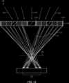
- FIG. 1 Aillustrates an example a cross section of a beam deflector metasurface 110 .
- the optical system 100may receive light 105 by the beam deflector metasurface 110 and direct the received light to a target area 103 .
- the beam deflector metasurface 110may include a unit cell, where the unit cell may be referred to herein as a “beam deflector” (the individual beam deflectors not specifically illustrated in FIG. 1 A ). It may be understood that the term “beam deflector metasurface” includes multiple beam deflectors arranged in concentric zones as well as the substrate upon which the beam deflectors are arranged. The beam deflectors may be arranged in a repeating pattern in a radial arrangement. The concentric zones are illustrated as a cross section in FIG. 1 A . The properties and features of the beam deflectors and beam deflector metasurfaces will be described herein with reference to FIGS. 1 A- 5 B .
- the beam deflector metasurface 110may direct the light to the target area 103 .
- the target area 103may not be the narrowest area or focal plane of the light.
- the target area 103may have a larger beam diameter than the beam diameter at the focal plane 104 , which is the narrowest intersection of the light after passing through the beam deflector metasurface 110 .
- the beam deflector metasurface 110functions as a non-focusing optic that may have improved efficiency at the far edges or the inside concentric zone 115 a and the outside concentric zone 115 b of the beam deflector metasurface 110 over using a conventional optical element.
- the angle at which the light may be directedmay be a higher angle than the light that passes through the beam inside concentric zone 115 a . Because of the concentric zone arrangement of the beam deflector metasurface 110 , light may be directed differently in each of the concentric zones 115 .
- a beam deflector metasurface 110may achieve higher efficiency with applications that use lenses with a large numerical aperture and long lens diameter (e.g., greater than approximately one mm diameter). Additionally, the beam deflector metasurface 110 may achieve improved performance over conventional optics and conventional metalenses for applications that employ non-normal angles of incidence.
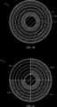
- FIG. 1 Billustrates an example top view of a beam deflector metasurface 110 .
- the beam deflector metasurfaceincludes concentric zones 115 .
- the inner concentric zone 115 a and the outer concentric zone 115 bmay direct light at different angles according to a predetermined or desired phase function.
- the phase functionmay repeat more often with large lens diameters and also may be periodic.
- the phase functionmay become closer and closer to periodic as the diameter of the angles increases.
- the beam deflector metasurface 110may have a lattice structure that matches the periodicity of the phase function, thus becoming a higher efficiency lens.
- the beam deflector metasurface 110exhibits symmetry both radially and angularly. Put another way, the radial function is the same regardless of the angular position sampled on the circular lattice.
- the circular lattice of the beam deflector metasurfacemay be radially and angularly symmetric.
- the beam deflector metasurface 110includes multiple concentric zones 115 , each of which may be capable of directing light at a different angle.
- Each of the concentric zonesmay be adjacent to one another and in some embodiments may be abutted to one another.
- the middle concentric zonessuch as concentric zone 115 c are illustrated as the same width, they may be the same width or varying widths depending on the predetermined phase function.
- the outer concentric zone 115 bmay direct light at a greater angle than the inner concentric zone 115 a .
- the circular latticeis illustrated, any shape lattice may be used such as square, hexagonal, octagonal, and so forth depending on the predetermined or desired phase function.
- the similar beam deflectorsmay be positioned in each of the hexagonal zones.
- the increased symmetry of the repeated beam deflector structures within the latticemay allow modeling of a large area metasurface (e.g., greater than approximately 500 microns).
- Each of the concentric zones 115may include multiple radially concentric layers of beam deflectors (not illustrated in FIG. 1 B ). Each beam deflector within a concentric ring may be identical to each other as well as the beam deflectors in each of the concentric rings that together form a concentric zone 115 . Similar to the concentric zones, as the concentric rings expand out in the radial pattern, the concentric rings may be adjacent to each other and may also be abutted to each other. As illustrated in FIG. 1 B , the beam deflector metasurface 110 may have concentric zones 115 that may be configured to direct light at any desired angle.
- the concentric zones 115may be designed so that the light passing through the concentric zone may be outputted to match the predetermined phase function of the target area.
- Each of the concentric zones 115 of the beam deflector metasurface 110may have different beam deflectors 120 . That is, the beam deflectors in a first concentric zone 115 may have a different number of pillars than the beam deflectors in a second concentric zone 115 . In another embodiment, the beam deflectors in a first concentric zone 115 may have the same number of pillars, but the size differential of the pillars may be different than the size differential of the pillars in a second concentric zone 115 .
- FIG. 1 Bis circular, any other shape may be used, such as an oval or racetrack shape, an asymmetric shape, or a configuration of beam deflectors as described with reference to FIG. 1 C and so forth.
- the concentric zone 115 bmay include a first set of beam deflectors arranged in a repeating pattern.
- the concentric zone 115 cmay be adjacent to concentric zone 115 b and may include a second set of beam deflectors arranged in a repeating pattern.
- the repeating pattern of the first set of beam deflectorsmay be the same as the repeating pattern of the second set of beam deflectors, while in other embodiments, the patterns in the first and second set of beam deflectors may not be the same as each other.
- FIG. 1 Cillustrates an example top view of a non-symmetric beam deflector metasurface 110 .
- the top left quadrant 160 amay achieve a different phase function than the other quadrants 160 b , 160 c , 160 d . That is, the top left quadrant 160 a may direct light to different angles than the other quadrants 160 b , 160 c , 160 d due to the positioning and size of the pillars in the beam deflectors.
- the top left quadrant 160 amay have different beam deflector structures than the beam deflectors of the other quadrants 160 b , 160 c , 160 d .
- the modularity of the beam deflector metasurface 110is advantageous as it may be specifically designed to address focal hot spots and beam detector over shoot and under shoot. In designing to reduce a focal hot spot, the beam deflector metasurface 110 may spread out the light in a particular area, direct light to a particular area and away from another area, and so forth. In other embodiments, each of the quadrants may differ from one another, two of the quadrants may be different from each other and from all of the other quadrants, and so forth.
- FIG. 2illustrates an example of a partial concentric zone 215 of a beam deflector metasurface.
- the partial concentric zone 215includes multiple repeating beam deflectors 205 .
- the beam deflectorshave four pillars 225 , but may include any number of pillars as appropriate for the desired phase function.
- the pillars 225may be spaced apart by a similar pitch, in other embodiments, the pitch may vary.
- the pillars 225may function as resonators and the cross-coupling between the pillars 225 may control the direction of the light passing through the beam deflector metasurface.
- the partial concentric zone 215includes two concentric rings 230 a , 230 b of beam deflectors 220 radially arranged. That is, the complete concentric zone (complete concentric zone is not illustrated in FIG. 2 ) includes multiple concentric rings 230 that form a ring so that the lattice of the complete beam deflector metasurface may be an r-theta type lattice.
- the beam deflectors 220may each have a first end near the smaller pillar and a second end near the larger pillar. As shown, the beam deflectors may be placed end to end, with a first end of one beam deflector near to, abutting, or adjacent to the second end of another beam deflector.
- each concentric ring 230 of the concentric zone 215may include the same pillar arrangement. Further, each concentric zone 215 may include beam deflectors with different pillar arrangements in each of the concentric zone 215 depending on the phase function.
- the arrangement of the beam deflectors 220may be similar to a lattice structure.
- the lattice structuremay be an r-theta lattice in that the beam deflector metasurface includes repeating structures in a radial pattern (e.g., each ring or concentric zone may include the same repeating beam deflectors) and also angularly in that a first quadrant (e.g., similar to the shape of a slice of pie) may include the same repeating structures as a second quadrant of the beam deflector metasurface.
- an r-theta lattice(e.g., a circular lattice) of the beam deflector metasurface may be radially and angularly symmetric.
- the use of the r-theta latticemay resolve a general mismatch between the phase function and other lattice shapes such as square or hexagonal.
- the lattice structuredepends largely on the predetermined phase function and may be any appropriate lattice such as square, hexagonal, octagonal, and so forth.
- the phase functionmay repeat periodically with large lens diameters so each of the concentric zones 215 may direct light to a specific angle.
- the lattice and the phase functionmay be “matched” in that the repeating phase function may be produced with the repeating lattice structure of each of the concentric zones of beam deflectors.
- each beam deflector 220is depicted as round, but may be a different shape.
- the shape, pitch, width, height, any combination thereof, and so forthmay affect the cross coupling between the pillars, thus affecting the angle at which the light passing through may be directed.
- the beam deflectors 220may each be rectangular because the beam deflector includes a one by four cell of pillars 225 .
- the beam deflectorsmay be other shapes that maintain periodicity when arranged in an r-theta lattice. As illustrated, the rectangular shape of the beam deflectors may result in a “fanning out” as the beam deflectors are arranged in larger concentric rings. Put another way, space between the beam deflectors (e.g., pitch error) may be introduced the further out radially the beam deflectors are positioned.
- the designmay maintain a periodic arrangement that reduces this pitch error until it reaches a critical point and then the pitch may be reset.
- FIG. 3illustrates an example of a side view of a beam deflector 320 with pillars 325 .
- the beam deflector 320may be a unit cell that is repeatedly arranged in the concentric zones of the beam deflector metasurface as described with reference to FIG. 1 A .
- the pillars 325may be different widths and the same height. It may be understood that although the pillars may be described as the “same height,” and the beam deflectors may be described herein as “identical” or “the same,” these elements may be as similar as may be achieved through the processing operations of fabricating the elements. That is, although the intent may be to manufacture identical or similar elements, there may be process fluctuations that introduce some variations in the elements. Although four pillars are illustrated in FIG. 3 , this is for discussion purposes only, as any appropriate number of pillars may be used in the beam deflectors.
- the beam deflector 320is a unit cell that includes one or more pillars 325 arranged on a substrate 326 .
- the pillars 325are arranged in a unit cell (e.g., a 1xn group of pillars), where the unit cell may be referred to herein as a “beam deflector.”
- beam deflector metasurfaceincludes multiple beam deflectors arranged in concentric zones as well as the substrate upon which the beam deflectors are arranged. This “chain” of pillars 325 of the beam deflector 320 may be arranged to target specific output angles to achieve a predetermined or desired phase function.
- the etch loadingmay be easier to model and/or predict due to the repeated pattern and the zoning of the beam deflector metasurface.
- the pillars and beam deflectorsmay be processed through the enabling of self-assembled metasurfaces or nano-imprints.
- the beam deflector metasurface structuremay allow for backfill material (e.g., liquid crystalline monomer) that may enable dynamic behavior, such as becoming electro-optically sensitive.
- the design of the pillars and the placement of the pillars and location and design of the beam deflector structuresmay be based on some other factor aside from achieving a predetermined phase function, such as the zoning of other shaped or asymmetric beam deflector metasurfaces. Further, by tuning the height of the pillars, the beam deflectors may be sensitive to wavelength and designed accordingly.
- the set of beam deflectorsmay include a set of pillars, where the height of the pillars may determines a wavelength sensitivity of the set of beam deflectors.
- the beam deflector 320may be repeatedly arranged in a radial pattern to direct light and achieve the predetermined phase function.
- the beam deflectors 320may be also used for typical lensing functions, but may achieve a more uniform output than phase functions produced by conventional metalenses. Put another way, the beam deflectors 320 may direct light in a way that reduces hot spots commonly produced when using conventional metalenses and classical optics. Due to the use of the radially arranged beam deflectors 320 , the far inner and outer concentric zones of the beam deflector metasurface may be designed to achieve high angle beam steering compared to that which is produced with known optics.
- the beam deflectors 320may be sensitive to polarization.
- the light passing through the beam deflector metasurfacemay be polarized along the direction of the arranged pillars as opposed to the orthogonal direction and the light may be affected differently. Because of this, the beam deflectors may be positioned to pass and block different polarizations of light.
- a set of beam deflectorsmay include a set of pillars that may allow light of a first polarization to pass in a first direction and attenuate light of a second polarization passing in a second direction. In this embodiment, the first direction may be orthogonal to the second direction.
- FIG. 4 Aillustrates a top view of an example beam deflector metasurface 410 .
- FIGS. 4 A and 4 Bwhich respectively illustrate a side view of a representative beam deflector in an outer concentric zone of the beam deflector metasurface of FIG. 4 A , and a side view of a representative beam deflector in an inner concentric zone of the beam deflector metasurface of FIG. 4 B .
- the inner and outer concentric zones 415 a and 415 bmay be narrower than the other concentric zones.
- the beam deflector metasurface 410may have radial and angular symmetry even though the inner and outer concentric zones 415 a , 415 b are narrower.
- the different widths of the concentric zones 415may be designed to achieve the predetermined or desired phase function.
- Each of the concentric zones 415may direct light at a different angle, or two of the concentric zones may direct light at the same angle, there may be a gradual or an abrupt angle change from concentric zone to concentric zone, and so forth.
- the seven concentric zones 415 shown in FIG. 4 Ainclude two different widths.
- the inner concentric zone 415 a and the outer concentric zone 415 bmay be the same width as one another and the other five concentric zones 415 may be the same width as one another.
- each of the concentric zonesmay be different widths from one another, three of the concentric zones may be the same width and the other concentric zones may be different widths, and so forth.
- the outer concentric zone 415 bmay direct the light at a steeper angle than the inner concentric zone 415 a .
- the concentric zones 415may direct light accordingly as will be described herein with reference to FIGS. 4 B and 4 C .
- the non-imaging application of FIG. 4 Amay receive light and direct the light to a defined range of angles of incidence.
- the lightmay be directed to a detector with an area on the order of around 100 microns.
- the outer concentric zone 415 bmay direct light at approximately 45 degrees with a short grating chain of four pillars and the inner concentric zone 415 a may direct the light at approximately 20 degrees with a longer grating chain of eight pillars. Due to the cross-coupling of the pillars, the performance and efficiency of the beam deflector metasurface may improve over the entire range of angles of incidence.
- the detector planemay be approximately 1.5 mm.
- Beam deflector metasurfacesare generally “flat” when compared to conventional optical elements and this “flat optic” structure may allow for multiple beneficial uses.
- One such usemay be the integration of the beam deflector metasurface with filters (e.g., anti-reflective filters, band pass filters, angular filters, and so forth).
- filterse.g., anti-reflective filters, band pass filters, angular filters, and so forth.
- an optical stack including a beam deflector metasurfacemay allow increased performance with a targeted diffractive order in addition to targeting the predetermined phase function alone.
- Another “flat optic” benefit of a beam deflector metasurfaceis the avoidance of shadowing due to the uniform height of the structure across the beam deflector metasurface.
- a beam deflector metasurfacemay be the ability to pattern the beam deflector metasurface onto other active devices (e.g., light sources such as vertical cavity surface emitting lasers, detectors, and so forth) and the ability to pattern active devices onto the beam deflector metasurface (e.g., failsafe traces).
- active devicese.g., light sources such as vertical cavity surface emitting lasers, detectors, and so forth
- the beam deflectorsmay be arranged in any type of repeating pattern, which may not be a radial and/or a concentric repeating pattern.
- FIG. 4 Bshows a beam deflector 410 a of the outer concentric zone 415 b of FIG. 4 A
- FIG. 4 Cshows a beam deflector 410 b of the inner concentric zone 415 a of FIG. 4 A
- the beam deflector 410 ahas four pillars 425 arranged on a substrate 462 a , where each pillar 425 is a different size from each other.
- the beam deflector 410 amay be positioned in a repeated, radial pattern as shown in FIG. 2 .
- Ten, twenty, hundreds, more or less than ten, and so forth of the beam deflectorsmay be positioned in a repeated, radial pattern in inner concentric zones 415 a .
- FIG. 4 Bshows a beam deflector 410 a of the outer concentric zone 415 b of FIG. 4 A
- FIG. 4 Cshows a beam deflector 410 b of the inner concentric zone 415 a of FIG. 4 A .
- the beam deflector 410 amay function as a four pillar grating that deflects light at an approximately 45 degree angle 414 a .
- the beam deflector 410 bhas eight pillars 425 arranged on a substrate 462 b that function as an eight pillar grating that directs light at an approximately 20 degree angle 414 b .
- the cross-coupling between the pillars or resonatorsmay improve efficiency over a wide range of angles.
- the beam deflector metasurfacemay function as a high numerical aperture, large diameter lens (e.g., approximately one mm).
- the beam deflector metasurfacesare useful for deteriorating focus, which may eliminate hot spots and spread the received light over the target area, such as a detector.
- the described beam deflector metasurfacesmay have improved efficiency at the edges due to the ability to direct light at a steeper angle and because of the radial design.
- the beam deflectorsmay be arranged in a repeated radial pattern, but it is to be understood that the beam deflectors may be arranged in any type of repeating pattern, which may not be radial and/or concentric.
- the pillars 425may all be different sizes, one pillar may be a different size from the other pillars, two pillars may be the same size and the other two may be different sizes, and so forth as may be dependent on the number of pillars.
- the pitchesmay be the same or varied as with the pillars. That is, the pitch between all of the pillars may be the same, one of the pitches may be different, two of the pitches between the pillars may be different, and so forth depending on the number of pillars.
- FIG. 4 Dillustrates a cross section of the beam deflector metasurface of FIG. 4 A directing light. Similar to FIG. 1 A , the beam deflector metasurface may direct light 423 to a target area 403 with a width that is less than the focal plane 404 of the direct light 423 . As previously described, the beam deflector metasurface 410 of FIGS. 4 A- 4 D may be designed for a deteriorating focus or non-imaging application. Also illustrated in FIG. 4 D , the outer concentric zone 415 b directs light at a sharper angle than the inner concentric zone 415 a .
- the light 423 passing through the beam deflector metasurface 410is shown as distinct beams, it may be understood that this is for illustrative and discussion purposes only and that the light may pass through the entire surface of the beam deflector metasurface and light may be directed by the entire surface of the beam deflector metasurface.
- FIG. 5 Aillustrates a side view of an optical system 500 with light passing through and being directed by a cross section of a beam deflector metasurface with zones 515 .
- the optical system 500may include a light source 540 that emits light toward a beam deflector metasurface 510 .
- the beam deflector metasurface 510includes multiple zones 515 .
- the beam deflector metasurface 510directs the light so that light may pass through the apertures 542 as opposed to being partially blocked by the areas 543 defining the apertures.
- Each of the zonesmay be designed with a repeating structure of beam deflectors to direct the light at the appropriate angle so that the light may pass through the apertures as will be described with reference to FIG. 5 B .
- the zonesmay be concentric zones as described herein.
- FIG. 5 Billustrates a partial cross section 501 of the zones 515 of the beam deflector metasurface 510 of FIG. 5 A .
- each of the zonesmay include three beam deflector zones. That is, a first beam deflector zone may include a first repeating beam deflector structure, a second beam deflector zone may include a second repeating beam deflector structure, and the third beam deflector zone may include a third repeating beam deflector structure.
- the three beam deflector zonesmay all be included in one zone of the beam deflector metasurface 510 .
- Each of the beam deflector zonesmay include multiple rings of the repeating, radially arranged beam deflectors, where the beam deflectors may be the same within the beam deflector zone.
- the rings of the beam deflectorsmay be concentric rings as described herein.
- the first beam deflector zone 550 amay include multiple rings of the same first beam deflector structure.
- the first beam deflector zone 550 amay include a first beam deflector structure with eight pillars of varying sizes.
- the first beam deflector structure with eight pillarsmay be repeatedly, radially arranged within the beam deflector zone 550 a .
- the second beam deflector zone 550 bmay include multiple rings of the same second beam deflector structure.
- the second beam deflector zone 550 bmay include a second beam deflector structure with six pillars of varying sizes, which may be repeated, radially arranged within the second beam deflector zone 550 b .
- the third beam deflector zone 550 cmay include a third beam deflector structure with four pillars of varying sizes, which may be repeatedly, radially arranged within the third beam deflector zone 550 c .
- the first, second, and third beam deflector zones 550 a , 550 b , 550 cmay be configured to direct light 523 at three different angles, where the third beam deflector zone 550 c may direct light 523 at a steeper angle than the first beam deflector zone 550 a .
- the design of the beam deflector zonesmay control the size of the focal spot width where the directed light may pass through the beam deflector zones 550 . This design may avoid hot spots and improve far field uniformity. This beam deflector geometry may improve the directed light paths to reduce stray light and improve the flexibility of the far field beam shaping.
- the first beam deflector zone 550 amay direct light at approximately an 18 degree angle
- the second beam deflector zone 550 bmay direct light at approximately a 27 degree angle
- the third beam deflector zone 550 cmay direct light at approximately a 36 degree angle, when the light received by the zone is in the range of 30-35 degrees.
- the lightmay be directed at less steep or steeper angles than the example depicted in FIG. 5 B .
- any sequence or order of steps that can be described in the disclosuredoes not, in and of itself, indicate a requirement that the steps be performed in that order. Further, some steps may be performed simultaneously despite being described or implied as occurring non-simultaneously (e.g., because one step is described after the other step).
- the illustration of a process by its description in a drawingdoes not imply that the illustrated process is exclusive of other variations and modification thereto, does not imply that the illustrated process or any of its steps are necessary to one or more of the examples, and does not imply that the illustrated process is preferred.
Landscapes
- Physics & Mathematics (AREA)
- General Physics & Mathematics (AREA)
- Optics & Photonics (AREA)
- Optical Elements Other Than Lenses (AREA)
- Diffracting Gratings Or Hologram Optical Elements (AREA)
Abstract
Description
- This disclosure relates generally to an optical device for improving stray light control and focal efficiency at non-normal angles. More particularly, embodiments herein relate to an optical device with radially arranged beam deflectors used for non-imaging applications.
- Generally, optical systems are used in various devices from mobile electronic devices to display technologies. Recently, there has been a trend toward reducing the form factor of some electronic devices by making them thinner and/or smaller. This poses a challenge for any electronic device that uses classical optics such as lenses and mirrors, which tend to be bulky optical elements. Although thinner optics have been developed as an alternative to bulky classical optics, some undesirable issues exist such as resulting hot spots. Additionally, the performance of these alternative optics degrade at non-normal angles of incidence, thus making an optical component with high efficiency at non-normal angles of incidence and a small form factor desirable.
- Embodiments of the systems, devices, methods, and apparatuses described in the present disclosure are directed to an optical element with highly efficient performance for high numerical aperture applications and non-normal angles of incidence. Also described are systems, devices, methods, and apparatuses directed to increased beam steering capabilities using beam deflector metasurfaces. In some examples, the optical element may include beam deflectors arranged in a radial coordinate system. The beam deflectors may be radially arranged insofar as all of the beam deflectors may have the same pillar arrangement and may be repeated in a radial pattern. The arrangement of the beam deflectors in the radial pattern may depend at least in part on a desired or predetermined output angle. Put another way, the light passing through the beam deflector metasurface may be steered at predetermined output angles and the corresponding beam deflector arrangement controls the direction in which the light is steered. The optical element may have concentric zones so that the first set of beam deflectors that are the same may be used in a first concentric zone, and a second set of beam deflectors that are the same to one another, but different than the first set of beam deflectors, may be used in a second concentric zone, where the concentric zones may be similar to concentric circles. Although two concentric zones may be discussed, any number of concentric zones may be used. Additionally, the optical element may be divided into angular zones where one or more of the angular zones may have a different set of beam deflectors than other angular zones. Using angular zones may be desirable for use in addressing atypical input irradiance patterns, achieving complex far field patterns, achieving uniform far field patterns, any combination thereof and so forth.
- In some examples, the present disclosure describes a beam deflector metasurface. The beam deflector metasurface may include a substrate, a first set of beam deflectors arranged on the substrate in a first concentric zone, and a second set of beam deflectors arranged on the substrate in a second concentric zone. The first set of beam deflectors may direct light passing through the beam deflector metasurface at a first angle, the second set of beam deflectors may direct light passing through the beam deflector metasurface at a second angle, the second concentric zone may be smaller in radius than the first concentric zone, and the first and second concentric zones may be arranged in concentric rings
- In some examples, the present disclosure describes a beam deflector metasurface. The beam deflector metasurface may include a first concentric zone, where the first concentric zone includes a first set of first beam deflectors arranged in a repeating pattern in the first concentric zone. The beam deflector metasurface may include a second concentric zone adjacent to the first concentric zone, where the second concentric zone may include a second set of second beam deflectors arranged in a repeating pattern in the second concentric zone. The first concentric zone may direct light passing through the beam deflector metasurface at a first angle via a first set of pillars and the second concentric zone may direct light passing through the beam deflector metasurface at a second angle via a second set of pillars, where the second angle is different than the first angle.
- In some examples, the present disclosure describes a method for directing light. The method may include receiving the light at a beam deflector metasurface with an inner concentric zone and an outer concentric zone, directing the light at a first angle from a first zone using a first set of beam deflectors arranged in a repeating pattern, and directing the light at a second angle from a second zone using a second set of beam deflectors arranged in a repeating pattern. In some embodiments, the first set of beam deflectors include a first set of pillars and each set of pillars in the first set of pillars are positioned in a first arrangement, and the second set of beam deflectors comprise a second set of pillars and each set of pillars in the second set of pillars are positioned in a second arrangement.
- In addition to the example aspects and embodiments described above, further aspects and embodiments will become apparent by reference to the drawings and by study of the following description.
FIG.1A illustrates an example cross section of a beam deflector metasurface.FIG.1B illustrates an example top view of a beam deflector metasurface.FIG.1C illustrates an example top view of a non-symmetric beam deflector metasurface.FIG.2 illustrates an example top view of a partial concentric zone of a beam deflector metasurface.FIG.3 illustrates an example beam deflector with pillars.FIG.4A illustrates a top view of an example beam deflector metasurface.FIG.4B illustrates a side view of a representative beam deflector in an outer concentric zone of the beam deflector metasurface ofFIG.4A .FIG.4C illustrates a side view of a representative beam deflector in an inner concentric zone of the beam deflector metasurface ofFIG.4A .FIG.4D illustrates a cross section of the beam deflector metasurface ofFIG.4A directing light.FIG.5A illustrates a side view of an optical system with light passing through and being directed by part of a beam deflector metasurface.FIG.5B illustrates a partial cross section of the beam deflector metasurface ofFIG.5A .- The use of cross-hatching or shading in the accompanying figures is generally provided to clarify the boundaries between adjacent elements and also to facilitate legibility of the figures. Accordingly, neither the presence nor the absence of cross-hatching or shading conveys or indicates any preference or requirement for particular materials, material properties, element proportions, element dimensions, commonalities of similarly illustrated elements, or any other characteristic, attribute, or property for any element illustrated in the accompanying figures.
- It should be understood that the proportions and dimensions (either relative or absolute) of the various features and elements (and collections and groupings thereof) and the boundaries, separations, and positional relationships presented between them, are provided in the accompanying figures merely to facilitate an understanding of the various embodiments described herein and, accordingly, may not necessarily be presented or illustrated to scale, and are not intended to indicate any preference or requirement for an illustrated embodiment to the exclusion of embodiments described with reference thereto.
- Reference will now be made in detail to representative embodiments illustrated in the accompanying drawings. It should be understood that the following description is not intended to limit the embodiments to one preferred embodiment. To the contrary, it is intended to cover alternatives, modifications, and equivalents as can be included within the spirit and scope of the described embodiments as defined by the appended claims.
- As used herein, the term “abutting” means that two elements share a common boundary or otherwise contact one another, while the term “adjacent” means that two elements are near one another and may (or may not) contact one another. Thus, elements that are abutting are also adjacent, although the reverse is not necessarily true. Two elements that are “coupled to” one another may be permanently or removably physically coupled to one another and/or operationally or functionally coupled to one another. Additionally, two elements that are “optically coupled” to one another may allow light to pass from one element to the other element.
- As used throughout this specification, a reference number without an alpha character following the reference number can refer to one or more of the corresponding references, the group of all references, or some of the references. For example, “305” can refer to one or more of the beam deflectors 305 (e.g., beam deflector 305a, beam deflector 305b, etc.), can refer to all of the beam deflectors 305, or can refer to some of the beam deflectors 305 (e.g., beam deflector 305a) depending on the context in which it is used.
- In the following description of examples, reference is made to the accompanying drawings in which it is shown by way of illustration specific examples that can be practiced. It is to be understood that other examples can be used and structural changes can be made without departing from the scope of the various examples.
- Conventional metalenses may include nanostructures on a substrate and the phase of the exiting light may depend largely on the overall response of the nanostructures or “pillars” on the substrate to light. The pillars on a conventional metalens may be arranged over the surface of the substrate in a pattern, so that the overall metalens structure may direct light according to the aggregate response of the pillars. The term “pillar” may be used herein and refers to the nanostructures on a substrate. For some optical systems, conventional metalenses are typically designed for imaging applications where the light is directed by the conventional metalenses at a normal incidence relative to the conventional metalens substrate and used for small numerical aperture lens and short lens diameter applications. Because the pillars are arranged in the aggregate over the substrate to achieve a phase function for directing light at normal incidences, performance may degrade for non-normal angles of incidence and at high numerical apertures and large areas.
- Disclosed herein is a beam deflector metasurface for directing light. The beam deflector metasurface may include numerous sets of beam deflectors positioned in a repeating arrangement, such as a lattice. Additionally, each beam deflector may include multiple pillars (e.g., 4 pillars, 6 pillars, 8 pillars, 13 pillars, or any other appropriate number). The pillars included in each beam deflector may vary in width, shape, height, have variable spacing, any combination thereof, and so forth within the structure of the beam deflector. In some embodiments, the lattice may be circular and the lattice shape may be based at least in part on a predetermined phase function. The phase function may give a predetermined or desired angular distribution of light intensity scattered by the beam deflectors. In some embodiments, the distribution of the light intensity may be a uniform distribution, a partially uniform distribution, or a non-uniform distribution. The beam deflector metasurface may function as a spatial transfer layer between the input and output angles of incidence of light.
- Generally metalenses may be flatter or planar and ultra-thin and offer advantages over classical optics. Metalenses may use the phase change that can be induced locally on a light wave by a small nano-sized feature such as the pillars or nanostructures discussed herein. These nanostructures or pillars may induce a phase change to light that passes through the metalens and the induced phase change may depend at least in part on the size, geometry, and arrangement of the pillars. Depending on the arrangement of the pillars or the distribution of the pillars on the substrate of the metasurface, the wavefront of an incoming light-wave can be shaped to almost any desired form. In this way, the light propagating through and away from the metasurface can be accurately controlled.
- The beam deflectors include multiple sets of pillars that may be the same or different sizes and heights. In an embodiment, the beam deflectors are arranged in a radial coordinate system. The beam deflectors may be radially arranged insofar as beam deflectors that all have the same pillar arrangement may be repeated in an overall radial and concentric pattern. In some embodiments, the beam deflectors may be arranged in a repeating pattern that may not be radial and/or concentric. The term “beam deflector structure” is used herein to refer to a beam deflector with a specific pillar arrangement. That is, the pillars within the beam deflector structure may all have a specific spacing, width, shape, height, and the same beam deflector structure indicates that each of the beam deflector structures have that particular pillar arrangement. The arrangement of the beam deflectors (e.g., the radial and/or concentric pattern) changes a phase function (e.g., output angle) of light passing through the beam deflector metasurface. Put another way, the light passing through the beam deflector metasurface may be steered at predetermined output angles that depend on a corresponding beam deflector structure and arrangement through which the light passes.
- The beam deflector metasurface may have one or more concentric rings within a concentric zone. In some embodiments, the one or more concentric rings within one concentric zone may have all the same beam deflector structure. That is, all the beam deflector structures (e.g., pillar arrangements of the beam deflector) may all be the same in a concentric ring, and all the beam deflector structures may be the same in the concentric zone. One or more concentric rings form a concentric zone. The beam deflectors may be radially arranged from the inner diameter to the outer diameter of the beam deflector metasurface and within a concentric zone. Put another way, the last pillar of a first beam deflector may be radially positioned and align with the first pillar of the second beam deflector, where the first beam deflector is closer to the center of the beam deflector metasurface than the second beam deflector. Generally, the first and last pillars of each beam deflector in a concentric ring are radially aligned with the first and last pillars of each adjacent first and last pillars of the adjacent concentric rings, thus they may “radiate” from the inner diameter to the outer diameter within the concentric zone. Further, the beam deflectors may have the same pillar arrangements and be radially arranged within a concentric zone so that when the beam deflector structure radially changes, so does the concentric zone. By way of explanation, in some embodiments, as the beam deflectors radiate and are aligned from the inner diameter to the outer diameter of the beam deflector metasurface, when the beam deflector structures are the same, they are in the same concentric zone, when the beam deflector structure changes to a different structure, that is a different concentric zone.
- In some embodiments, radial zones so that a first set of identical first beam deflectors may be used in a first concentric zone and a second set of identical second beam deflectors to each other, but the first and second beam deflectors of the first and second sets may be different from one another. Additionally, the second concentric zones may be concentric about the first concentric zone and the first and second sets of beam deflectors have different physical properties. Further, the first concentric zone and the second concentric zone may be adjacent to one another. In other examples, the first concentric zone and the second concentric zone may be abutted to one another. Although first and second concentric zones may be described herein, any number of concentric zones may be used.
- A beam deflector may include pillars that function similar to diffractive gratings and that cross-couple with one another to direct the light. The pillars may be the same or different widths, may be the same or different heights, may have a pitch between the pillars that is the same or varies, and may be circular, square, rectangular, or any other appropriate shape. In some embodiments, a beam deflector metasurface may include multiple concentric zones. Each concentric zone may include one or more concentric rings and the concentric rings include a repeating lattice of beam deflectors. That is, a first beam deflector structure may be radially arranged in each of the concentric rings. There may be ten, fifteen, twenty, fewer, or more concentric rings within a concentric zone and the concentric rings may include a first type of beam deflector structure. Different concentric zones may include different beam deflector structures and may include a different or the same number of concentric rings as other concentric zones. Further, the concentric zones may be the same or different widths.
- Additionally, the beam deflector metasurface may be divided into angular zones (e.g., quadrants, octants, and so forth) where one or more of the angular zones may have a different set of beam deflectors than other angular zones. Put another way, one quadrant of a circular beam deflector metasurface may have a different phase function than the other A beam deflector metasurface with such angular zones may be useful in addressing atypical input irradiance patterns, achieving complex far field patterns, achieving uniform far field patterns, any combination thereof, and so forth.
- The beam deflector metasurface may be a large area, high numerical aperture metasurface optic that may be configured to direct light towards a target with high efficiency across non-normal angles of incidence. In an example, the target phase function that may be used to design the beam deflectors may have a zero to two pi phase shift over a distance that may be mapped to a range of target detection angles. The beam deflector metasurface may be capable of achieving the zero to two pi phase shift over the same distance.
- These and other embodiments are discussed below with reference to
FIGS.1A-5B . However, those skilled in the art will readily appreciate that the detailed description given herein with respect to these Figures is for explanatory purposes only and should not be construed as limiting. FIG.1A illustrates an example a cross section of abeam deflector metasurface 110. Theoptical system 100 may receive light105 by thebeam deflector metasurface 110 and direct the received light to atarget area 103. Thebeam deflector metasurface 110 may include a unit cell, where the unit cell may be referred to herein as a “beam deflector” (the individual beam deflectors not specifically illustrated inFIG.1A ). It may be understood that the term “beam deflector metasurface” includes multiple beam deflectors arranged in concentric zones as well as the substrate upon which the beam deflectors are arranged. The beam deflectors may be arranged in a repeating pattern in a radial arrangement. The concentric zones are illustrated as a cross section inFIG.1A . The properties and features of the beam deflectors and beam deflector metasurfaces will be described herein with reference toFIGS.1A-5B .- In the optical system of
FIG.1A , thebeam deflector metasurface 110 may direct the light to thetarget area 103. As shown, thetarget area 103 may not be the narrowest area or focal plane of the light. Put another way, thetarget area 103 may have a larger beam diameter than the beam diameter at thefocal plane 104, which is the narrowest intersection of the light after passing through thebeam deflector metasurface 110. In the example ofFIG.1A , thebeam deflector metasurface 110 functions as a non-focusing optic that may have improved efficiency at the far edges or the insideconcentric zone 115a and the outsideconcentric zone 115b of thebeam deflector metasurface 110 over using a conventional optical element. As shown by the light passing through the outsideconcentric zone 115b of thebeam deflector metasurface 110, the angle at which the light may be directed may be a higher angle than the light that passes through the beam insideconcentric zone 115a. Because of the concentric zone arrangement of thebeam deflector metasurface 110, light may be directed differently in each of the concentric zones115. - Additionally, the use of a
beam deflector metasurface 110 may achieve higher efficiency with applications that use lenses with a large numerical aperture and long lens diameter (e.g., greater than approximately one mm diameter). Additionally, thebeam deflector metasurface 110 may achieve improved performance over conventional optics and conventional metalenses for applications that employ non-normal angles of incidence. FIG.1B illustrates an example top view of abeam deflector metasurface 110. The beam deflector metasurface includes concentric zones115. The innerconcentric zone 115a and the outerconcentric zone 115b may direct light at different angles according to a predetermined or desired phase function. In some embodiments, the phase function may repeat more often with large lens diameters and also may be periodic. The phase function may become closer and closer to periodic as the diameter of the angles increases. Thebeam deflector metasurface 110 may have a lattice structure that matches the periodicity of the phase function, thus becoming a higher efficiency lens. Thebeam deflector metasurface 110 exhibits symmetry both radially and angularly. Put another way, the radial function is the same regardless of the angular position sampled on the circular lattice. In some embodiments, the circular lattice of the beam deflector metasurface may be radially and angularly symmetric.- As shown, the
beam deflector metasurface 110 includes multiple concentric zones115, each of which may be capable of directing light at a different angle. Each of the concentric zones may be adjacent to one another and in some embodiments may be abutted to one another. Although the middle concentric zones such asconcentric zone 115c are illustrated as the same width, they may be the same width or varying widths depending on the predetermined phase function. In an example, the outerconcentric zone 115b may direct light at a greater angle than the innerconcentric zone 115a. Although the circular lattice is illustrated, any shape lattice may be used such as square, hexagonal, octagonal, and so forth depending on the predetermined or desired phase function. In an example, if a hexagonal lattice is employed, the similar beam deflectors may be positioned in each of the hexagonal zones. The increased symmetry of the repeated beam deflector structures within the lattice may allow modeling of a large area metasurface (e.g., greater than approximately 500 microns). - Each of the concentric zones115 may include multiple radially concentric layers of beam deflectors (not illustrated in
FIG.1B ). Each beam deflector within a concentric ring may be identical to each other as well as the beam deflectors in each of the concentric rings that together form a concentric zone115. Similar to the concentric zones, as the concentric rings expand out in the radial pattern, the concentric rings may be adjacent to each other and may also be abutted to each other. As illustrated inFIG.1B , thebeam deflector metasurface 110 may have concentric zones115 that may be configured to direct light at any desired angle. Further, the concentric zones115 may be designed so that the light passing through the concentric zone may be outputted to match the predetermined phase function of the target area. Each of the concentric zones115 of thebeam deflector metasurface 110 may have different beam deflectors120. That is, the beam deflectors in a first concentric zone115 may have a different number of pillars than the beam deflectors in a second concentric zone115. In another embodiment, the beam deflectors in a first concentric zone115 may have the same number of pillars, but the size differential of the pillars may be different than the size differential of the pillars in a second concentric zone115. Although the embodiment ofFIG.1B is circular, any other shape may be used, such as an oval or racetrack shape, an asymmetric shape, or a configuration of beam deflectors as described with reference toFIG.1C and so forth. - As shown in
FIG.1B , theconcentric zone 115b may include a first set of beam deflectors arranged in a repeating pattern. Theconcentric zone 115c may be adjacent toconcentric zone 115b and may include a second set of beam deflectors arranged in a repeating pattern. In some embodiments the repeating pattern of the first set of beam deflectors may be the same as the repeating pattern of the second set of beam deflectors, while in other embodiments, the patterns in the first and second set of beam deflectors may not be the same as each other. FIG.1C illustrates an example top view of a non-symmetricbeam deflector metasurface 110. Comparing thebeam deflector metasurface 110 ofFIG.1C with that ofFIG.1B , the topleft quadrant 160a may achieve a different phase function than theother quadrants left quadrant 160a may direct light to different angles than theother quadrants - In this example, the top
left quadrant 160a may have different beam deflector structures than the beam deflectors of theother quadrants beam deflector metasurface 110 is advantageous as it may be specifically designed to address focal hot spots and beam detector over shoot and under shoot. In designing to reduce a focal hot spot, thebeam deflector metasurface 110 may spread out the light in a particular area, direct light to a particular area and away from another area, and so forth. In other embodiments, each of the quadrants may differ from one another, two of the quadrants may be different from each other and from all of the other quadrants, and so forth. FIG.2 illustrates an example of a partialconcentric zone 215 of a beam deflector metasurface. The partialconcentric zone 215 includes multiple repeatingbeam deflectors 205. As illustrated, the beam deflectors have fourpillars 225, but may include any number of pillars as appropriate for the desired phase function. Additionally, although thepillars 225 may be spaced apart by a similar pitch, in other embodiments, the pitch may vary. Thepillars 225 may function as resonators and the cross-coupling between thepillars 225 may control the direction of the light passing through the beam deflector metasurface.- The partial
concentric zone 215 includes twoconcentric rings FIG.2 ) includes multiple concentric rings230 that form a ring so that the lattice of the complete beam deflector metasurface may be an r-theta type lattice. The beam deflectors220 may each have a first end near the smaller pillar and a second end near the larger pillar. As shown, the beam deflectors may be placed end to end, with a first end of one beam deflector near to, abutting, or adjacent to the second end of another beam deflector. The beam deflectors in each concentric ring230 of theconcentric zone 215 may include the same pillar arrangement. Further, eachconcentric zone 215 may include beam deflectors with different pillar arrangements in each of theconcentric zone 215 depending on the phase function. - Although only two concentric rings of partial
concentric zones 215 are illustrated inFIG.2 , there may be many more layers of beam deflectors220 that are in aconcentric zone 215. The arrangement of the beam deflectors220 may be similar to a lattice structure. The lattice structure may be an r-theta lattice in that the beam deflector metasurface includes repeating structures in a radial pattern (e.g., each ring or concentric zone may include the same repeating beam deflectors) and also angularly in that a first quadrant (e.g., similar to the shape of a slice of pie) may include the same repeating structures as a second quadrant of the beam deflector metasurface. In some embodiments, an r-theta lattice (e.g., a circular lattice) of the beam deflector metasurface may be radially and angularly symmetric. The use of the r-theta lattice may resolve a general mismatch between the phase function and other lattice shapes such as square or hexagonal. With that said, the lattice structure depends largely on the predetermined phase function and may be any appropriate lattice such as square, hexagonal, octagonal, and so forth. In an example, the phase function may repeat periodically with large lens diameters so each of theconcentric zones 215 may direct light to a specific angle. In other words, the lattice and the phase function may be “matched” in that the repeating phase function may be produced with the repeating lattice structure of each of the concentric zones of beam deflectors. - The
pillars 225 of each beam deflector220 are depicted as round, but may be a different shape. The shape, pitch, width, height, any combination thereof, and so forth may affect the cross coupling between the pillars, thus affecting the angle at which the light passing through may be directed. - Further, the beam deflectors220 may each be rectangular because the beam deflector includes a one by four cell of
pillars 225. The beam deflectors may be other shapes that maintain periodicity when arranged in an r-theta lattice. As illustrated, the rectangular shape of the beam deflectors may result in a “fanning out” as the beam deflectors are arranged in larger concentric rings. Put another way, space between the beam deflectors (e.g., pitch error) may be introduced the further out radially the beam deflectors are positioned. In an example, the design may maintain a periodic arrangement that reduces this pitch error until it reaches a critical point and then the pitch may be reset. FIG.3 illustrates an example of a side view of abeam deflector 320 withpillars 325. Thebeam deflector 320 may be a unit cell that is repeatedly arranged in the concentric zones of the beam deflector metasurface as described with reference toFIG.1A . As shown in the embodiment ofFIG.3 , thepillars 325 may be different widths and the same height. It may be understood that although the pillars may be described as the “same height,” and the beam deflectors may be described herein as “identical” or “the same,” these elements may be as similar as may be achieved through the processing operations of fabricating the elements. That is, although the intent may be to manufacture identical or similar elements, there may be process fluctuations that introduce some variations in the elements. Although four pillars are illustrated inFIG.3 , this is for discussion purposes only, as any appropriate number of pillars may be used in the beam deflectors.- The
beam deflector 320 is a unit cell that includes one ormore pillars 325 arranged on asubstrate 326. Thepillars 325 are arranged in a unit cell (e.g., a 1xn group of pillars), where the unit cell may be referred to herein as a “beam deflector.” It may be understood that the term “beam deflector metasurface” includes multiple beam deflectors arranged in concentric zones as well as the substrate upon which the beam deflectors are arranged. This “chain” ofpillars 325 of thebeam deflector 320 may be arranged to target specific output angles to achieve a predetermined or desired phase function. - By employing repeated unit cell beam deflector structures, the etch loading may be easier to model and/or predict due to the repeated pattern and the zoning of the beam deflector metasurface. In other embodiments, the pillars and beam deflectors may be processed through the enabling of self-assembled metasurfaces or nano-imprints. Furthermore, the beam deflector metasurface structure may allow for backfill material (e.g., liquid crystalline monomer) that may enable dynamic behavior, such as becoming electro-optically sensitive.
- Additionally, the design of the pillars and the placement of the pillars and location and design of the beam deflector structures may be based on some other factor aside from achieving a predetermined phase function, such as the zoning of other shaped or asymmetric beam deflector metasurfaces. Further, by tuning the height of the pillars, the beam deflectors may be sensitive to wavelength and designed accordingly. In some embodiments, the set of beam deflectors may include a set of pillars, where the height of the pillars may determines a wavelength sensitivity of the set of beam deflectors.
- The
beam deflector 320 may be repeatedly arranged in a radial pattern to direct light and achieve the predetermined phase function. The beam deflectors320 may be also used for typical lensing functions, but may achieve a more uniform output than phase functions produced by conventional metalenses. Put another way, thebeam deflectors 320 may direct light in a way that reduces hot spots commonly produced when using conventional metalenses and classical optics. Due to the use of the radially arrangedbeam deflectors 320, the far inner and outer concentric zones of the beam deflector metasurface may be designed to achieve high angle beam steering compared to that which is produced with known optics. - Additionally, the
beam deflectors 320 may be sensitive to polarization. The light passing through the beam deflector metasurface may be polarized along the direction of the arranged pillars as opposed to the orthogonal direction and the light may be affected differently. Because of this, the beam deflectors may be positioned to pass and block different polarizations of light. In some embodiments, a set of beam deflectors may include a set of pillars that may allow light of a first polarization to pass in a first direction and attenuate light of a second polarization passing in a second direction. In this embodiment, the first direction may be orthogonal to the second direction. FIG.4A illustrates a top view of an examplebeam deflector metasurface 410. Also shown areFIGS.4A and4B , which respectively illustrate a side view of a representative beam deflector in an outer concentric zone of the beam deflector metasurface ofFIG.4A , and a side view of a representative beam deflector in an inner concentric zone of the beam deflector metasurface ofFIG.4B . The inner and outerconcentric zones beam deflector metasurface 410 may have radial and angular symmetry even though the inner and outerconcentric zones FIG.4A include two different widths. The innerconcentric zone 415a and the outerconcentric zone 415b may be the same width as one another and the other five concentric zones415 may be the same width as one another. In other embodiments, each of the concentric zones may be different widths from one another, three of the concentric zones may be the same width and the other concentric zones may be different widths, and so forth. Additionally, there may be fewer or more concentric zones depending on the predetermined phase function to be achieved and the size of the target area. In the embodiment ofFIG.4A , the outerconcentric zone 415b may direct the light at a steeper angle than the innerconcentric zone 415a. Depending on the predetermined phase function, the concentric zones415 may direct light accordingly as will be described herein with reference toFIGS.4B and4C .- The non-imaging application of
FIG.4A , may receive light and direct the light to a defined range of angles of incidence. In an example, the light may be directed to a detector with an area on the order of around 100 microns. Thus, in the example ofFIG.4A , the outerconcentric zone 415b may direct light at approximately 45 degrees with a short grating chain of four pillars and the innerconcentric zone 415a may direct the light at approximately 20 degrees with a longer grating chain of eight pillars. Due to the cross-coupling of the pillars, the performance and efficiency of the beam deflector metasurface may improve over the entire range of angles of incidence. In other embodiments, the detector plane may be approximately 1.5 mm. - One of the desirable qualities of beam deflector metasurfaces is the optical performance that may be achieved without the penalty of thick conventional optics. Beam deflector metasurfaces are generally “flat” when compared to conventional optical elements and this “flat optic” structure may allow for multiple beneficial uses. One such use may be the integration of the beam deflector metasurface with filters (e.g., anti-reflective filters, band pass filters, angular filters, and so forth). In an embodiment, an optical stack including a beam deflector metasurface may allow increased performance with a targeted diffractive order in addition to targeting the predetermined phase function alone. Another “flat optic” benefit of a beam deflector metasurface is the avoidance of shadowing due to the uniform height of the structure across the beam deflector metasurface. Additionally, another advantageous use of a beam deflector metasurface may be the ability to pattern the beam deflector metasurface onto other active devices (e.g., light sources such as vertical cavity surface emitting lasers, detectors, and so forth) and the ability to pattern active devices onto the beam deflector metasurface (e.g., failsafe traces). It should be understood that the beam deflectors may be arranged in any type of repeating pattern, which may not be a radial and/or a concentric repeating pattern.
FIG.4B shows abeam deflector 410a of the outerconcentric zone 415b ofFIG.4A andFIG.4C shows abeam deflector 410b of the innerconcentric zone 415a ofFIG.4A . Thebeam deflector 410a has fourpillars 425 arranged on asubstrate 462a, where eachpillar 425 is a different size from each other. Thebeam deflector 410a may be positioned in a repeated, radial pattern as shown inFIG.2 . Ten, twenty, hundreds, more or less than ten, and so forth of the beam deflectors may be positioned in a repeated, radial pattern in innerconcentric zones 415a. In the example ofFIG.4B , thebeam deflector 410a may function as a four pillar grating that deflects light at an approximately 45degree angle 414a. InFIG.4C , thebeam deflector 410b has eightpillars 425 arranged on asubstrate 462b that function as an eight pillar grating that directs light at an approximately 20degree angle 414b.- As previously described, the cross-coupling between the pillars or resonators may improve efficiency over a wide range of angles. By arranging these beam deflectors in a repeated radial pattern, the beam deflector metasurface may function as a high numerical aperture, large diameter lens (e.g., approximately one mm). Further, the beam deflector metasurfaces are useful for deteriorating focus, which may eliminate hot spots and spread the received light over the target area, such as a detector. Additionally, the described beam deflector metasurfaces may have improved efficiency at the edges due to the ability to direct light at a steeper angle and because of the radial design. As described herein, the beam deflectors may be arranged in a repeated radial pattern, but it is to be understood that the beam deflectors may be arranged in any type of repeating pattern, which may not be radial and/or concentric.
- In other embodiments, the
pillars 425 may all be different sizes, one pillar may be a different size from the other pillars, two pillars may be the same size and the other two may be different sizes, and so forth as may be dependent on the number of pillars. Similarly, the pitches may be the same or varied as with the pillars. That is, the pitch between all of the pillars may be the same, one of the pitches may be different, two of the pitches between the pillars may be different, and so forth depending on the number of pillars. FIG.4D illustrates a cross section of the beam deflector metasurface ofFIG.4A directing light. Similar toFIG.1A , the beam deflector metasurface may direct light423 to atarget area 403 with a width that is less than thefocal plane 404 of thedirect light 423. As previously described, thebeam deflector metasurface 410 ofFIGS.4A-4D may be designed for a deteriorating focus or non-imaging application. Also illustrated inFIG.4D , the outerconcentric zone 415b directs light at a sharper angle than the innerconcentric zone 415a. Although the light423 passing through thebeam deflector metasurface 410 is shown as distinct beams, it may be understood that this is for illustrative and discussion purposes only and that the light may pass through the entire surface of the beam deflector metasurface and light may be directed by the entire surface of the beam deflector metasurface.FIG.5A illustrates a side view of anoptical system 500 with light passing through and being directed by a cross section of a beam deflector metasurface withzones 515. Theoptical system 500 may include alight source 540 that emits light toward abeam deflector metasurface 510. Thebeam deflector metasurface 510 includesmultiple zones 515. Thebeam deflector metasurface 510 directs the light so that light may pass through theapertures 542 as opposed to being partially blocked by theareas 543 defining the apertures. Each of the zones may be designed with a repeating structure of beam deflectors to direct the light at the appropriate angle so that the light may pass through the apertures as will be described with reference toFIG.5B . In some embodiments, the zones may be concentric zones as described herein.FIG.5B illustrates apartial cross section 501 of thezones 515 of thebeam deflector metasurface 510 ofFIG.5A . As shown inFIG.5B , each of the zones may include three beam deflector zones. That is, a first beam deflector zone may include a first repeating beam deflector structure, a second beam deflector zone may include a second repeating beam deflector structure, and the third beam deflector zone may include a third repeating beam deflector structure. The three beam deflector zones may all be included in one zone of thebeam deflector metasurface 510. Each of the beam deflector zones may include multiple rings of the repeating, radially arranged beam deflectors, where the beam deflectors may be the same within the beam deflector zone. In some embodiments, the rings of the beam deflectors may be concentric rings as described herein.- In
FIG.5B , the firstbeam deflector zone 550a may include multiple rings of the same first beam deflector structure. Put another way, the firstbeam deflector zone 550a may include a first beam deflector structure with eight pillars of varying sizes. The first beam deflector structure with eight pillars may be repeatedly, radially arranged within thebeam deflector zone 550a. The secondbeam deflector zone 550b may include multiple rings of the same second beam deflector structure. The secondbeam deflector zone 550b may include a second beam deflector structure with six pillars of varying sizes, which may be repeated, radially arranged within the secondbeam deflector zone 550b. The thirdbeam deflector zone 550c may include a third beam deflector structure with four pillars of varying sizes, which may be repeatedly, radially arranged within the thirdbeam deflector zone 550c. The first, second, and thirdbeam deflector zones beam deflector zone 550c may direct light523 at a steeper angle than the firstbeam deflector zone 550a. The design of the beam deflector zones may control the size of the focal spot width where the directed light may pass through the beam deflector zones550. This design may avoid hot spots and improve far field uniformity. This beam deflector geometry may improve the directed light paths to reduce stray light and improve the flexibility of the far field beam shaping. - In the embodiment of
FIG.5B , the firstbeam deflector zone 550a may direct light at approximately an 18 degree angle, the secondbeam deflector zone 550b may direct light at approximately a 27 degree angle, and the thirdbeam deflector zone 550c may direct light at approximately a 36 degree angle, when the light received by the zone is in the range of 30-35 degrees. Depending on the design of the beam deflector structures and the configuration of the beam deflector structures within the zones, the light may be directed at less steep or steeper angles than the example depicted inFIG.5B . - Further, although process steps or method steps can be described in a sequential order, such processes and methods can be configured to work in any suitable order. In other words, any sequence or order of steps that can be described in the disclosure does not, in and of itself, indicate a requirement that the steps be performed in that order. Further, some steps may be performed simultaneously despite being described or implied as occurring non-simultaneously (e.g., because one step is described after the other step). Moreover, the illustration of a process by its description in a drawing does not imply that the illustrated process is exclusive of other variations and modification thereto, does not imply that the illustrated process or any of its steps are necessary to one or more of the examples, and does not imply that the illustrated process is preferred.
- Representative applications of methods and apparatuses according to the present disclosure are described in this section. These examples are being provided solely to add context and aid in the understanding of the described examples. It will thus be apparent to one skilled in the art that the described examples may be practiced without some or all of the specific details. Other applications are possible, such that the following examples should not be taken as limiting.
- Although the disclosed examples have been fully described with reference to the accompanying drawings, it is to be noted that various changes and modifications will become apparent to those skilled in the art. Such changes and modifications are to be understood as being included within the scope of the disclosed examples as defined by the appended claims.
Claims (20)
Priority Applications (4)
| Application Number | Priority Date | Filing Date | Title |
|---|---|---|---|
| US17/466,813US12124002B2 (en) | 2021-09-03 | 2021-09-03 | Beam deflector metasurface |
| JP2022120661AJP7611192B2 (en) | 2021-09-03 | 2022-07-28 | Beam deflector metasurface |
| EP22189269.8AEP4145188A1 (en) | 2021-09-03 | 2022-08-08 | Beam deflector metasurface |
| KR1020220106014AKR20230034890A (en) | 2021-09-03 | 2022-08-24 | Beam deflector metasurface |
Applications Claiming Priority (1)
| Application Number | Priority Date | Filing Date | Title |
|---|---|---|---|
| US17/466,813US12124002B2 (en) | 2021-09-03 | 2021-09-03 | Beam deflector metasurface |
Publications (2)
| Publication Number | Publication Date |
|---|---|
| US20230070943A1true US20230070943A1 (en) | 2023-03-09 |
| US12124002B2 US12124002B2 (en) | 2024-10-22 |
Family
ID=82850294
Family Applications (1)
| Application Number | Title | Priority Date | Filing Date |
|---|---|---|---|
| US17/466,813Active2041-11-22US12124002B2 (en) | 2021-09-03 | 2021-09-03 | Beam deflector metasurface |
Country Status (4)
| Country | Link |
|---|---|
| US (1) | US12124002B2 (en) |
| EP (1) | EP4145188A1 (en) |
| JP (1) | JP7611192B2 (en) |
| KR (1) | KR20230034890A (en) |
Cited By (4)
| Publication number | Priority date | Publication date | Assignee | Title |
|---|---|---|---|---|
| US11839133B2 (en) | 2021-03-12 | 2023-12-05 | Apple Inc. | Organic photodetectors for in-cell optical sensing |
| US12016237B2 (en) | 2019-09-24 | 2024-06-18 | Apple Inc. | Display stack with integrated photodetectors |
| WO2025050849A1 (en)* | 2023-09-05 | 2025-03-13 | 苏州山河光电科技有限公司 | Tof emission module and tof system having same |
| WO2025056319A1 (en)* | 2023-09-14 | 2025-03-20 | Safran Electronics & Defense | Helical-phase optronic angle error measurement device |
Citations (7)
| Publication number | Priority date | Publication date | Assignee | Title |
|---|---|---|---|---|
| US20140044392A1 (en)* | 2011-04-20 | 2014-02-13 | David A Fattal | Sub-wavelength grating-based optical elements |
| US20160299337A1 (en)* | 2015-04-08 | 2016-10-13 | Samsung Electronics Co., Ltd. | Focusing device, and beam scanner and scope device including the focusing device |
| US20160353039A1 (en)* | 2015-05-27 | 2016-12-01 | Verily Life Sciences Llc | Nanophotonic Hyperspectral/Lightfield Superpixel Imager |
| US20190154877A1 (en)* | 2016-04-05 | 2019-05-23 | President And Fellows Of Harvard College | Meta-lenses for sub-wavelength resolution imaging |
| US20210103075A1 (en)* | 2019-10-08 | 2021-04-08 | Samsung Electronics Co., Ltd. | Meta lens and optical apparatus including the same |
| US20210149081A1 (en)* | 2017-05-04 | 2021-05-20 | President And Fellows Of Harvard College | Meta-lens doublet for aberration correction |
| US20210337140A1 (en)* | 2020-04-27 | 2021-10-28 | Samsung Electronics Co., Ltd. | Optical device for a thermal sensor and a hybrid thermal sensor |
Family Cites Families (157)
| Publication number | Priority date | Publication date | Assignee | Title |
|---|---|---|---|---|
| US5231689A (en) | 1983-10-04 | 1993-07-27 | Tru-Lyte Systems, Inc. | Wide angle viewing illuminated information display assembly and process for manufacturing same |
| JPS6127447U (en) | 1984-07-24 | 1986-02-19 | 富士電機株式会社 | Squirrel cage rotor with air duct |
| US5194986A (en) | 1992-03-23 | 1993-03-16 | Hughes Aircraft Company | Objective lens assembly for a portable missile launcher |
| JPH09152840A (en) | 1995-11-29 | 1997-06-10 | Sanesu:Kk | Illuminator for display part of sign, symbol, picture, and the like |
| JP2001021992A (en) | 1999-07-09 | 2001-01-26 | C Media:Kk | Mobile terminal, mobile terminal system and mobile phone |
| US6349159B1 (en) | 1999-09-02 | 2002-02-19 | Agilent Technologies, Inc. | Lenses that launch high bandwidth modes into a fiber optic cable while eliminating feedback to a laser |
| US6780661B1 (en) | 2000-04-12 | 2004-08-24 | Finisar Corporation | Integration of top-emitting and top-illuminated optoelectronic devices with micro-optic and electronic integrated circuits |
| DE10033485C2 (en) | 2000-07-10 | 2003-10-23 | Infineon Technologies Ag | Coupling glass fiber for optically coupling a light radiation source to a multimode optical waveguide, optoelectronic light transmission component for multimode optical waveguide and manufacturing process for coupling glass windows |
| US6677709B1 (en) | 2000-07-18 | 2004-01-13 | General Electric Company | Micro electromechanical system controlled organic led and pixel arrays and method of using and of manufacturing same |
| US6946647B1 (en) | 2000-08-10 | 2005-09-20 | Raytheon Company | Multicolor staring missile sensor system |
| US6556349B2 (en) | 2000-12-27 | 2003-04-29 | Honeywell International Inc. | Variable focal length micro lens array field curvature corrector |
| US6910812B2 (en) | 2001-05-15 | 2005-06-28 | Peregrine Semiconductor Corporation | Small-scale optoelectronic package |
| DK2461156T3 (en) | 2001-06-29 | 2020-08-03 | Meso Scale Technologies Llc | Device for luminescence test measurements |
| US7071615B2 (en) | 2001-08-20 | 2006-07-04 | Universal Display Corporation | Transparent electrodes |
| US6921920B2 (en) | 2001-08-31 | 2005-07-26 | Smith & Nephew, Inc. | Solid-state light source |
| CN1620626A (en) | 2002-01-21 | 2005-05-25 | 松下电器产业株式会社 | Optical switch, manufacturing method thereof, and information transmission device using same |
| US20030148391A1 (en) | 2002-01-24 | 2003-08-07 | Salafsky Joshua S. | Method using a nonlinear optical technique for detection of interactions involving a conformational change |
| US7021833B2 (en) | 2002-03-22 | 2006-04-04 | Ban-Poh Loh | Waveguide based optical coupling of a fiber optic cable and an optoelectronic device |
| US20040067324A1 (en) | 2002-09-13 | 2004-04-08 | Lazarev Pavel I | Organic photosensitive optoelectronic device |
| KR200312616Y1 (en) | 2003-02-21 | 2003-05-12 | 변진성 | Lighting apparatus of camera to take photograph of the uterine cervical region |
| US20040209116A1 (en) | 2003-04-21 | 2004-10-21 | Xiaofan Ren | Organic light emitting devices with wide gap host materials |
| US6919681B2 (en) | 2003-04-30 | 2005-07-19 | Eastman Kodak Company | Color OLED display with improved power efficiency |
| JP3729353B2 (en) | 2003-06-18 | 2005-12-21 | 松下電器産業株式会社 | Solid-state imaging device and manufacturing method thereof |
| JP2005049830A (en) | 2003-07-14 | 2005-02-24 | Fuji Photo Film Co Ltd | Optical signal transmission system |
| US6948820B2 (en) | 2003-08-28 | 2005-09-27 | Scram Technologies, Inc. | Interactive display system having an optical channeling element |
| KR100582504B1 (en) | 2003-08-29 | 2006-05-23 | 이동미 | Device for guiding camera flash light |
| US7495272B2 (en) | 2003-10-06 | 2009-02-24 | Semiconductor Energy Labortaory Co., Ltd. | Semiconductor device having photo sensor element and amplifier circuit |
| CA2990275C (en) | 2003-11-21 | 2023-01-03 | Visual Physics, Llc | Micro-optic security and image presentation system |
| DE202004002512U1 (en) | 2004-02-13 | 2005-03-10 | Meschke, Holger | Fiber-optic lamp for illuminating objects being photographed, has light emitting ends of optical fibers arranged in ring, e.g. around lens |
| GB0406107D0 (en) | 2004-03-17 | 2004-04-21 | Koninkl Philips Electronics Nv | Electroluminescent display devices |
| JP3984639B2 (en) | 2005-03-30 | 2007-10-03 | 松下電器産業株式会社 | Transmission line |
| JP2009500662A (en) | 2005-06-29 | 2009-01-08 | リフレキサイト・コーポレーション | Collimating microlens array |
| US7712906B1 (en) | 2006-07-06 | 2010-05-11 | Roy Larimer | Macro flash adapter |
| JP4582166B2 (en) | 2008-03-19 | 2010-11-17 | ソニー株式会社 | Display device |
| JP5624987B2 (en) | 2008-09-09 | 2014-11-12 | テクニオン リサーチ アンド ディベロップメント ファウンデーションリミテッド | Derivatized fullerene-based dopants for organic semiconductors |
| US8441007B2 (en) | 2008-12-25 | 2013-05-14 | Semiconductor Energy Laboratory Co., Ltd. | Display device and manufacturing method thereof |
| JP2010231937A (en) | 2009-03-26 | 2010-10-14 | Kyocera Corp | Portable electronic devices |
| US8603642B2 (en) | 2009-05-13 | 2013-12-10 | Global Oled Technology Llc | Internal connector for organic electronic devices |
| US8624853B2 (en) | 2009-06-01 | 2014-01-07 | Perceptive Pixel Inc. | Structure-augmented touch sensing with frustated total internal reflection |
| US8749528B2 (en) | 2009-06-25 | 2014-06-10 | Sharp Kabushiki Kaisha | Display device |
| TWI523240B (en) | 2009-08-24 | 2016-02-21 | 半導體能源研究所股份有限公司 | Photodetector and display device |
| US20120113357A1 (en) | 2009-11-06 | 2012-05-10 | Chimei Innolux Corp. | Transmissive Liquid Crystal Display with Reflective Mode |
| JP5028501B2 (en) | 2010-01-20 | 2012-09-19 | 株式会社ジャパンディスプレイイースト | Liquid crystal display |
| KR101108167B1 (en) | 2010-02-12 | 2012-02-06 | 삼성모바일디스플레이주식회사 | Organic light emitting display device |
| EP2463927B1 (en) | 2010-12-08 | 2013-08-21 | Novaled AG | Material for organic electronic device and organic electronic device |
| US8743027B2 (en) | 2011-08-30 | 2014-06-03 | E Ink Holdings Inc. | OLED driving circuit and method of the same used in display panel |
| KR20130050605A (en) | 2011-11-08 | 2013-05-16 | 삼성전자주식회사 | Display panel and portable device |
| US9342181B2 (en) | 2012-01-09 | 2016-05-17 | Nvidia Corporation | Touch-screen input/output device touch sensing techniques |
| US9064451B2 (en) | 2012-02-01 | 2015-06-23 | Apple Inc. | Organic light emitting diode display having photodiodes |
| US9183779B2 (en) | 2012-02-23 | 2015-11-10 | Broadcom Corporation | AMOLED light sensing |
| US9633247B2 (en) | 2012-03-01 | 2017-04-25 | Apple Inc. | Electronic device with shared near field communications and sensor structures |
| US9431621B2 (en) | 2012-03-13 | 2016-08-30 | The Regents Of The University Of Michigan | Metal oxide charge transport material doped with organic molecules |
| US9235057B2 (en) | 2012-05-18 | 2016-01-12 | Reald Inc. | Polarization recovery in a directional display device |
| US8780065B2 (en) | 2012-07-19 | 2014-07-15 | Cypress Semiconductor Corporation | Interface and synchronization method between touch controller and display driver for operation with touch integrated displays |
| JP6127447B2 (en) | 2012-10-29 | 2017-05-17 | 大日本印刷株式会社 | OPTICAL LAMINATE, DISPLAY DEVICE FRONT PLATE, DISPLAY DEVICE, RESISTANCE FILM TYPE TOUCH AND CAPACITANCE TYPE TOUCH |
| US9279947B2 (en) | 2012-11-15 | 2016-03-08 | 4233999 Canada Inc. | Methods and apparatus for high speed short distance optical communications using micro light emitting diodes |
| US9070648B2 (en) | 2012-11-27 | 2015-06-30 | Apple Inc. | Electronic devices with display-integrated light sensors |
| TWI547834B (en) | 2012-11-29 | 2016-09-01 | 鴻海精密工業股份有限公司 | Writing apparatus and light-emitting diode display panel and emitting device thereof |
| US9530381B1 (en) | 2012-12-20 | 2016-12-27 | Amazon Technologies, Inc. | Display with light sensor feedback |
| US9310843B2 (en) | 2013-01-02 | 2016-04-12 | Apple Inc. | Electronic devices with light sensors and displays |
| JP6300442B2 (en) | 2013-01-18 | 2018-03-28 | オリンパス株式会社 | Optical transmission module and imaging device |
| TWI549322B (en) | 2013-04-10 | 2016-09-11 | 映瑞光電科技(上海)有限公司 | Integrated LED component combined with epitaxial structure and package substrate and manufacturing method thereof |
| KR101883541B1 (en) | 2013-06-17 | 2018-07-30 | 도판 인사츠 가부시키가이샤 | Substrate for display device, and display device using same |
| EP3022633A4 (en) | 2013-07-19 | 2017-04-12 | Hewlett-Packard Development Company, L.P. | Light guide panel including diffraction gratings |
| JP6116005B2 (en) | 2013-08-27 | 2017-04-19 | 国立大学法人東京工業大学 | Method for producing metamaterial |
| JP6192465B2 (en) | 2013-09-27 | 2017-09-06 | ホシデン株式会社 | Touch panel and display device |
| JP6639416B2 (en) | 2014-02-07 | 2020-02-05 | セーエヌアーエム‐コンセルバトワール、ナショナル、デ、ザール、エ、メティエCnam−Conservatoire National Des Arts Et Metiers | Method for manufacturing a vertical optical coupling structure |
| WO2015130226A1 (en) | 2014-02-25 | 2015-09-03 | Heptagon Micro Optics Pte. Ltd. | Image sensor modules including primary high-resolution imagers and secondary imagers |
| TWI518434B (en) | 2014-04-25 | 2016-01-21 | 元太科技工業股份有限公司 | Display device |
| US9836165B2 (en) | 2014-05-16 | 2017-12-05 | Apple Inc. | Integrated silicon-OLED display and touch sensor panel |
| US9741286B2 (en) | 2014-06-03 | 2017-08-22 | Apple Inc. | Interactive display panel with emitting and sensing diodes |
| US9570002B2 (en) | 2014-06-17 | 2017-02-14 | Apple Inc. | Interactive display panel with IR diodes |
| KR102260600B1 (en) | 2014-12-31 | 2021-06-04 | 엘지디스플레이 주식회사 | Touch screen device |
| US9614168B2 (en) | 2015-01-12 | 2017-04-04 | Apple Inc. | Flexible display panel with bent substrate |
| US10565734B2 (en) | 2015-04-15 | 2020-02-18 | Google Llc | Video capture, processing, calibration, computational fiber artifact removal, and light-field pipeline |
| US10410037B2 (en) | 2015-06-18 | 2019-09-10 | Shenzhen GOODIX Technology Co., Ltd. | Under-screen optical sensor module for on-screen fingerprint sensing implementing imaging lens, extra illumination or optical collimator array |
| CN107004130B (en) | 2015-06-18 | 2020-08-28 | 深圳市汇顶科技股份有限公司 | Optical sensor module under screen for sensing fingerprint on screen |
| HK1251716A1 (en) | 2015-06-19 | 2019-02-01 | 德累斯顿工业技术大学 | Organic photodetectors and production method thereof |
| US10670790B2 (en) | 2015-08-11 | 2020-06-02 | Michael Braithwaite | System and method for illuminating and identifying an object |
| TWI575808B (en) | 2015-08-24 | 2017-03-21 | 吳家和 | Isolation structure of microstrip for reducing crosstalk |
| US10345905B2 (en) | 2015-09-08 | 2019-07-09 | Apple Inc. | Electronic devices with deformable displays |
| EP3353578B1 (en) | 2015-09-23 | 2021-01-20 | OSRAM Opto Semiconductors GmbH | Collimating metalenses and technologies incorporating the same |
| US9934418B2 (en) | 2015-12-03 | 2018-04-03 | Synaptics Incorporated | Display integrated optical fingerprint sensor with angle limiting reflector |
| US10115000B2 (en) | 2015-12-11 | 2018-10-30 | Synaptics Incorporated | Method and system for optical imaging using patterned illumination |
| TW201800459A (en) | 2015-12-18 | 2018-01-01 | 富士軟片股份有限公司 | Near-infrared absorption composition, near-infrared cut filter, near-infrared cut filter manufacturing method, solid-state imaging device, camera module, and image display device |
| CN108700797B (en) | 2016-01-12 | 2020-12-08 | 株式会社可乐丽 | Head-up display and method of making the same |
| CN115458571A (en) | 2016-01-21 | 2022-12-09 | 苹果公司 | Power and data routing structure for organic light emitting diode display |
| CN107145253B (en) | 2016-02-19 | 2020-06-09 | 苹果公司 | Force Sensing Architecture |
| US10289891B2 (en) | 2016-03-31 | 2019-05-14 | Synaptics Incorpated | Optical biometric sensor having diffractive optical elements |
| CN107292215A (en) | 2016-03-31 | 2017-10-24 | 上海箩箕技术有限公司 | Optical fingerprint sensor module |
| US10108841B2 (en) | 2016-03-31 | 2018-10-23 | Synaptics Incorporated | Biometric sensor with diverging optical element |
| JP6792960B2 (en) | 2016-05-16 | 2020-12-02 | 株式会社ジャパンディスプレイ | Display device |
| US10713458B2 (en) | 2016-05-23 | 2020-07-14 | InSyte Systems | Integrated light emitting display and sensors for detecting biologic characteristics |
| CN109074475B (en) | 2016-05-23 | 2022-03-01 | 苹果公司 | Electronic device including pinhole array mask and related methods |
| CN105867696B (en) | 2016-06-03 | 2020-11-17 | 京东方科技集团股份有限公司 | Touch display panel, flexible display panel and display device |
| GB201609877D0 (en) | 2016-06-06 | 2016-07-20 | Microsoft Technology Licensing Llc | An autonomous pixel with multiple different sensors |
| US9909862B2 (en) | 2016-06-13 | 2018-03-06 | Google Llc | Curved array of light-emitting elements for sweeping out an angular range |
| WO2018002784A1 (en) | 2016-06-29 | 2018-01-04 | Semiconductor Energy Laboratory Co., Ltd. | Electronic device, operation method of the electronic device, and moving vehicle |
| WO2018002774A1 (en) | 2016-06-29 | 2018-01-04 | Semiconductor Energy Laboratory Co., Ltd. | Electronic device, operation method of the electronic device, and moving vehicle |
| US20180032778A1 (en) | 2016-07-29 | 2018-02-01 | Microsoft Technology Licensing, Llc | Display with a touch sensor |
| KR102576813B1 (en) | 2016-10-07 | 2023-09-11 | 삼성전자주식회사 | Touch screen display and electronic device including the same |
| WO2018072176A1 (en) | 2016-10-20 | 2018-04-26 | 3M Innovative Properties Company | Device optical window camouflage |
| US10474286B2 (en) | 2016-10-25 | 2019-11-12 | Lg Display Co., Ltd. | Touch display device, active pen, touch system, touch circuit, and pen recognition method |
| US20210319197A1 (en) | 2016-11-15 | 2021-10-14 | Bidirectional Display Inc. | Apparatus and method for optically capturing fingerprint or other images on display screen |
| CN106886767B (en) | 2017-02-23 | 2019-07-05 | 京东方科技集团股份有限公司 | A kind of optical fingerprint identification device and display panel |
| CN109791325B (en) | 2017-03-07 | 2022-02-08 | 深圳市汇顶科技股份有限公司 | Device with peripheral taskbar display and LCD underscreen optical sensor module for on-screen fingerprint sensing |
| CN107068716B (en) | 2017-03-31 | 2020-04-07 | 京东方科技集团股份有限公司 | Integrated display panel, manufacturing method and display device |
| KR102330096B1 (en) | 2017-04-06 | 2021-11-23 | 삼성전자 주식회사 | A method and an electronic device for acquiring biometric information during a period when video data is not transmitted to a display |
| US20180323243A1 (en) | 2017-05-02 | 2018-11-08 | Boe Technology Group Co., Ltd. | Array substrate, image collection method and display device |
| DE202018006696U1 (en) | 2017-05-15 | 2022-04-01 | Ouster, Inc. | Optical image transmitter with brightness improvement |
| WO2018210317A1 (en) | 2017-05-17 | 2018-11-22 | Shenzhen GOODIX Technology Co., Ltd. | Optical fingerprint sensor with non-touch imaging capability |
| US10614279B2 (en) | 2017-06-02 | 2020-04-07 | Samsung Electronics Co., Ltd. | Apparatus and method for driving fingerprint sensing array provided in touchscreen, and driver integrated circuit for driving the touchscreen including the fingerprint sensing array |
| US10664676B2 (en) | 2017-06-12 | 2020-05-26 | Will Semiconductor (Shanghai) Co. Ltd. | Systems and methods for reducing unwanted reflections in display systems incorporating an under display biometric sensor |
| CN109216421B (en) | 2017-07-04 | 2023-10-24 | 三星电子株式会社 | Organic light emitting diode panel and display device including the same |
| US10331939B2 (en) | 2017-07-06 | 2019-06-25 | Shenzhen GOODIX Technology Co., Ltd. | Multi-layer optical designs of under-screen optical sensor module having spaced optical collimator array and optical sensor array for on-screen fingerprint sensing |
| KR102441588B1 (en) | 2017-07-10 | 2022-09-07 | 삼성전자주식회사 | Beam scanning device and optical device including same |
| CN107180853B (en) | 2017-07-10 | 2020-05-12 | 京东方科技集团股份有限公司 | An OLED display panel, control method thereof, and display device |
| KR102449825B1 (en) | 2017-07-31 | 2022-10-04 | 삼성전자주식회사 | Display for fingerprint recognition and electronic apparatus |
| KR101835819B1 (en) | 2017-08-11 | 2018-03-08 | 주식회사 에이엘테크 | Light emitting sign apparatus using optical fiber |
| KR102486389B1 (en) | 2017-08-14 | 2023-01-09 | 삼성전자주식회사 | nanostructured optical element comprising, depth sensor and electronic device |
| CN107330426B (en) | 2017-08-28 | 2024-03-29 | 京东方科技集团股份有限公司 | Fingerprint identification device, display panel and fingerprint identification method |
| CN107515435B (en) | 2017-09-11 | 2020-12-29 | 京东方科技集团股份有限公司 | Display panels and display devices |
| KR102510916B1 (en) | 2017-11-02 | 2023-03-17 | 삼성디스플레이 주식회사 | Display device and method of driving the display device |
| JP7013216B2 (en) | 2017-11-28 | 2022-01-31 | 株式会社ジャパンディスプレイ | Display device |
| US10809853B2 (en) | 2017-12-11 | 2020-10-20 | Will Semiconductor (Shanghai) Co. Ltd. | Optical sensor having apertures |
| CN108648691B (en) | 2018-05-14 | 2020-03-20 | 上海天马有机发光显示技术有限公司 | Display panel, driving method thereof and display device |
| CN110488315B (en) | 2018-05-14 | 2023-09-12 | Sos实验株式会社 | Laser output device and lidar device |
| KR102590315B1 (en) | 2018-05-28 | 2023-10-16 | 삼성전자주식회사 | Organic photoelectric device and image sensor including the same |
| US10411797B1 (en) | 2018-06-08 | 2019-09-10 | SA Photonics, Inc. | Free space optical node with fiber bundle |
| KR102508792B1 (en) | 2018-08-07 | 2023-03-13 | 엘지디스플레이 주식회사 | Display device |
| CN108922918B (en) | 2018-09-10 | 2021-01-26 | 京东方科技集团股份有限公司 | An OLED display panel and its manufacturing method, and an OLED display device |
| US10840320B2 (en) | 2018-09-28 | 2020-11-17 | Apple Inc. | Ambient light sensing display assemblies |
| EP3637472B1 (en) | 2018-10-08 | 2025-07-02 | Samsung Electronics Co., Ltd. | Organic light emitting diode display panels and display devices including the same |
| US11815703B2 (en) | 2018-12-03 | 2023-11-14 | Samsung Electronics Co., Ltd. | Meta-lens and optical apparatus including the same |
| US11067884B2 (en) | 2018-12-26 | 2021-07-20 | Apple Inc. | Through-display optical transmission, reception, or sensing through micro-optic elements |
| EP3686630A1 (en) | 2019-01-25 | 2020-07-29 | IDT Inc. | Proximity sensor, particularly for mobile devices like smartphones, tablets or the like |
| CN109983471B (en) | 2019-02-02 | 2020-09-18 | 深圳市汇顶科技股份有限公司 | Fingerprint identification devices and electronic equipment |
| EP3888204B1 (en) | 2019-02-04 | 2022-12-14 | Apple Inc. | Vertical emitters with integral microlenses |
| US11301665B2 (en) | 2019-02-20 | 2022-04-12 | Novatek Microelectronics Corp. | Fingerprint and proximity sensing apparatus and sensing process thereof |
| WO2020178923A1 (en) | 2019-03-01 | 2020-09-10 | シャープ株式会社 | Display device |
| US10838556B2 (en) | 2019-04-05 | 2020-11-17 | Apple Inc. | Sensing system for detection of light incident to a light emitting layer of an electronic device display |
| US11659758B2 (en) | 2019-07-05 | 2023-05-23 | Semiconductor Energy Laboratory Co., Ltd. | Display unit, display module, and electronic device |
| US20210050385A1 (en) | 2019-08-13 | 2021-02-18 | Apple Inc. | Photodetectors Integrated into Thin-Film Transistor Backplanes |
| US11394014B2 (en) | 2019-08-29 | 2022-07-19 | Semiconductor Energy Laboratory Co., Ltd. | Display unit, display module, and electronic device |
| US20210089741A1 (en) | 2019-09-23 | 2021-03-25 | Apple Inc. | Thin-Film Transistor Optical Imaging System with Integrated Optics for Through-Display Biometric Imaging |
| US11611058B2 (en) | 2019-09-24 | 2023-03-21 | Apple Inc. | Devices and systems for under display image sensor |
| US11527582B1 (en) | 2019-09-24 | 2022-12-13 | Apple Inc. | Display stack with integrated photodetectors |
| KR20210064483A (en) | 2019-11-25 | 2021-06-03 | 삼성디스플레이 주식회사 | Display panel having input sensing function and display device |
| US12072511B2 (en) | 2020-02-07 | 2024-08-27 | Samsung Electronics Co., Ltd. | Meta-lens, image capturing lens including the meta-lens, image capturing device including the image capturing lens, and electronic apparatus including the image capturing device |
| US11592873B2 (en) | 2020-02-14 | 2023-02-28 | Apple Inc. | Display stack topologies for under-display optical transceivers |
| US11295664B2 (en) | 2020-03-11 | 2022-04-05 | Apple Inc. | Display-synchronized optical emitters and transceivers |
| US11327237B2 (en) | 2020-06-18 | 2022-05-10 | Apple Inc. | Display-adjacent optical emission or reception using optical fibers |
| US11487859B2 (en) | 2020-07-31 | 2022-11-01 | Apple Inc. | Behind display polarized optical transceiver |
| KR20220030004A (en) | 2020-09-02 | 2022-03-10 | 엘지디스플레이 주식회사 | Display panel and display device using the same |
| CN112505808B (en) | 2020-12-09 | 2021-10-08 | 华中科技大学 | A long-wave infrared broadband achromatic metasurface lens |
| US11839133B2 (en) | 2021-03-12 | 2023-12-05 | Apple Inc. | Organic photodetectors for in-cell optical sensing |
| US20230034270A1 (en) | 2021-07-28 | 2023-02-02 | Apple Inc. | Optical Fiber Illumination by a Set of Light Emitters |
- 2021
- 2021-09-03USUS17/466,813patent/US12124002B2/enactiveActive
- 2022
- 2022-07-28JPJP2022120661Apatent/JP7611192B2/enactiveActive
- 2022-08-08EPEP22189269.8Apatent/EP4145188A1/enactivePending
- 2022-08-24KRKR1020220106014Apatent/KR20230034890A/enactivePending
Patent Citations (7)
| Publication number | Priority date | Publication date | Assignee | Title |
|---|---|---|---|---|
| US20140044392A1 (en)* | 2011-04-20 | 2014-02-13 | David A Fattal | Sub-wavelength grating-based optical elements |
| US20160299337A1 (en)* | 2015-04-08 | 2016-10-13 | Samsung Electronics Co., Ltd. | Focusing device, and beam scanner and scope device including the focusing device |
| US20160353039A1 (en)* | 2015-05-27 | 2016-12-01 | Verily Life Sciences Llc | Nanophotonic Hyperspectral/Lightfield Superpixel Imager |
| US20190154877A1 (en)* | 2016-04-05 | 2019-05-23 | President And Fellows Of Harvard College | Meta-lenses for sub-wavelength resolution imaging |
| US20210149081A1 (en)* | 2017-05-04 | 2021-05-20 | President And Fellows Of Harvard College | Meta-lens doublet for aberration correction |
| US20210103075A1 (en)* | 2019-10-08 | 2021-04-08 | Samsung Electronics Co., Ltd. | Meta lens and optical apparatus including the same |
| US20210337140A1 (en)* | 2020-04-27 | 2021-10-28 | Samsung Electronics Co., Ltd. | Optical device for a thermal sensor and a hybrid thermal sensor |
Cited By (5)
| Publication number | Priority date | Publication date | Assignee | Title |
|---|---|---|---|---|
| US12016237B2 (en) | 2019-09-24 | 2024-06-18 | Apple Inc. | Display stack with integrated photodetectors |
| US11839133B2 (en) | 2021-03-12 | 2023-12-05 | Apple Inc. | Organic photodetectors for in-cell optical sensing |
| WO2025050849A1 (en)* | 2023-09-05 | 2025-03-13 | 苏州山河光电科技有限公司 | Tof emission module and tof system having same |
| WO2025056319A1 (en)* | 2023-09-14 | 2025-03-20 | Safran Electronics & Defense | Helical-phase optronic angle error measurement device |
| FR3153161A1 (en)* | 2023-09-14 | 2025-03-21 | Safran Electronics & Defense | Optronic helical phase deviation measurement device. |
Also Published As
| Publication number | Publication date |
|---|---|
| EP4145188A1 (en) | 2023-03-08 |
| JP7611192B2 (en) | 2025-01-09 |
| JP2023037577A (en) | 2023-03-15 |
| KR20230034890A (en) | 2023-03-10 |
| US12124002B2 (en) | 2024-10-22 |
Similar Documents
| Publication | Publication Date | Title |
|---|---|---|
| US12124002B2 (en) | Beam deflector metasurface | |
| CN107703579B (en) | Metasurface lens for realizing lateral multifocal focusing and its realization method | |
| JP7248662B2 (en) | optical beamformer | |
| US12092791B2 (en) | Optical metalens systems | |
| US20180154482A1 (en) | Laser processing apparatus | |
| JP7601815B2 (en) | Meta-optical devices, optical systems, and methods for aberration correction | |
| KR20200129034A (en) | Meta lens and optical apparatus including the same | |
| US10481328B1 (en) | Optical phased array with integrated secondary optics | |
| US20220342118A1 (en) | Acoustic luneburg meta lens and design method thereof | |
| CN113330339A (en) | Diffractive optical element, and projection apparatus and measurement apparatus using the same | |
| WO2011143015A1 (en) | Optical beam shaping devices using microfacets | |
| KR20070018918A (en) | Device and method for optical beam homogenization | |
| US11874476B1 (en) | Metalens collimators and condensers | |
| US12306424B2 (en) | Metasurface-based imaging system, design method, and detector | |
| CN103048716A (en) | Single stage focusing wave zone plate and manufacturing method thereof | |
| US20250015474A1 (en) | Metalens | |
| CN103293677B (en) | Light homogenizer and manufacturing method thereof | |
| US20170080607A1 (en) | Angled light source with uniform broad area illumination | |
| US7672050B2 (en) | Refractive index controlled diffractive optical element and its manufacturing method | |
| CN114442439A (en) | An integrated ultraviolet all-dielectric metalens group for lithography machine | |
| US20150168612A1 (en) | Substrate for display device, method for fabricating the same, and display device including the same | |
| JP4380590B2 (en) | Multi-stage diffractive optical element | |
| CN119301475A (en) | Measuring device, irradiation device and bandpass filter | |
| TWI716216B (en) | Bessel beam homogenization module | |
| CN114706151A (en) | A polarization-maintaining broad-spectrum focusing mid-infrared metalens based on a biomimetic moth-eye structure |
Legal Events
| Date | Code | Title | Description |
|---|---|---|---|
| AS | Assignment | Owner name:APPLE INC., CALIFORNIA Free format text:ASSIGNMENT OF ASSIGNORS INTEREST;ASSIGNORS:GE, ZHENBIN;ZHANG, RUNYU;SIGNING DATES FROM 20210830 TO 20210903;REEL/FRAME:057386/0263 Owner name:APPLE INC., CALIFORNIA Free format text:ASSIGNMENT OF ASSIGNORS INTEREST;ASSIGNORS:VULIS, DARYL I.;HUI, BRANDON J.;OCIER, CHRISTIAN;AND OTHERS;SIGNING DATES FROM 20210824 TO 20210831;REEL/FRAME:057386/0092 | |
| FEPP | Fee payment procedure | Free format text:ENTITY STATUS SET TO UNDISCOUNTED (ORIGINAL EVENT CODE: BIG.); ENTITY STATUS OF PATENT OWNER: LARGE ENTITY | |
| STPP | Information on status: patent application and granting procedure in general | Free format text:FINAL REJECTION MAILED | |
| STPP | Information on status: patent application and granting procedure in general | Free format text:RESPONSE AFTER FINAL ACTION FORWARDED TO EXAMINER | |
| STPP | Information on status: patent application and granting procedure in general | Free format text:ADVISORY ACTION MAILED | |
| STPP | Information on status: patent application and granting procedure in general | Free format text:DOCKETED NEW CASE - READY FOR EXAMINATION | |
| STPP | Information on status: patent application and granting procedure in general | Free format text:NON FINAL ACTION MAILED | |
| STPP | Information on status: patent application and granting procedure in general | Free format text:RESPONSE TO NON-FINAL OFFICE ACTION ENTERED AND FORWARDED TO EXAMINER | |
| STPP | Information on status: patent application and granting procedure in general | Free format text:FINAL REJECTION MAILED | |
| STPP | Information on status: patent application and granting procedure in general | Free format text:DOCKETED NEW CASE - READY FOR EXAMINATION | |
| STPP | Information on status: patent application and granting procedure in general | Free format text:NOTICE OF ALLOWANCE MAILED -- APPLICATION RECEIVED IN OFFICE OF PUBLICATIONS | |
| ZAAB | Notice of allowance mailed | Free format text:ORIGINAL CODE: MN/=. | |
| STPP | Information on status: patent application and granting procedure in general | Free format text:NOTICE OF ALLOWANCE MAILED -- APPLICATION RECEIVED IN OFFICE OF PUBLICATIONS | |
| STPP | Information on status: patent application and granting procedure in general | Free format text:PUBLICATIONS -- ISSUE FEE PAYMENT VERIFIED | |
| STCF | Information on status: patent grant | Free format text:PATENTED CASE |