US20220399206A1 - Method for building conductive through-hole vias in glass substrates - Google Patents
Method for building conductive through-hole vias in glass substratesDownload PDFInfo
- Publication number
- US20220399206A1 US20220399206A1US17/724,317US202217724317AUS2022399206A1US 20220399206 A1US20220399206 A1US 20220399206A1US 202217724317 AUS202217724317 AUS 202217724317AUS 2022399206 A1US2022399206 A1US 2022399206A1
- Authority
- US
- United States
- Prior art keywords
- circuitry
- conductor
- coating
- applying
- glass substrate
- Prior art date
- Legal status (The legal status is an assumption and is not a legal conclusion. Google has not performed a legal analysis and makes no representation as to the accuracy of the status listed.)
- Abandoned
Links
Images


Classifications
- H—ELECTRICITY
- H01—ELECTRIC ELEMENTS
- H01L—SEMICONDUCTOR DEVICES NOT COVERED BY CLASS H10
- H01L21/00—Processes or apparatus adapted for the manufacture or treatment of semiconductor or solid state devices or of parts thereof
- H01L21/02—Manufacture or treatment of semiconductor devices or of parts thereof
- H01L21/04—Manufacture or treatment of semiconductor devices or of parts thereof the devices having potential barriers, e.g. a PN junction, depletion layer or carrier concentration layer
- H01L21/48—Manufacture or treatment of parts, e.g. containers, prior to assembly of the devices, using processes not provided for in a single one of the groups H01L21/18 - H01L21/326 or H10D48/04 - H10D48/07
- H01L21/4814—Conductive parts
- H01L21/4846—Leads on or in insulating or insulated substrates, e.g. metallisation
- H01L21/486—Via connections through the substrate with or without pins
- H—ELECTRICITY
- H01—ELECTRIC ELEMENTS
- H01L—SEMICONDUCTOR DEVICES NOT COVERED BY CLASS H10
- H01L21/00—Processes or apparatus adapted for the manufacture or treatment of semiconductor or solid state devices or of parts thereof
- H01L21/02—Manufacture or treatment of semiconductor devices or of parts thereof
- H01L21/04—Manufacture or treatment of semiconductor devices or of parts thereof the devices having potential barriers, e.g. a PN junction, depletion layer or carrier concentration layer
- H01L21/18—Manufacture or treatment of semiconductor devices or of parts thereof the devices having potential barriers, e.g. a PN junction, depletion layer or carrier concentration layer the devices having semiconductor bodies comprising elements of Group IV of the Periodic Table or AIIIBV compounds with or without impurities, e.g. doping materials
- H01L21/30—Treatment of semiconductor bodies using processes or apparatus not provided for in groups H01L21/20 - H01L21/26
- H01L21/31—Treatment of semiconductor bodies using processes or apparatus not provided for in groups H01L21/20 - H01L21/26 to form insulating layers thereon, e.g. for masking or by using photolithographic techniques; After treatment of these layers; Selection of materials for these layers
- H01L21/3105—After-treatment
- H01L21/311—Etching the insulating layers by chemical or physical means
- H01L21/31105—Etching inorganic layers
- H01L21/31111—Etching inorganic layers by chemical means
- H—ELECTRICITY
- H01—ELECTRIC ELEMENTS
- H01L—SEMICONDUCTOR DEVICES NOT COVERED BY CLASS H10
- H01L21/00—Processes or apparatus adapted for the manufacture or treatment of semiconductor or solid state devices or of parts thereof
- H01L21/02—Manufacture or treatment of semiconductor devices or of parts thereof
- H01L21/027—Making masks on semiconductor bodies for further photolithographic processing not provided for in group H01L21/18 or H01L21/34
- H01L21/0271—Making masks on semiconductor bodies for further photolithographic processing not provided for in group H01L21/18 or H01L21/34 comprising organic layers
- H01L21/0273—Making masks on semiconductor bodies for further photolithographic processing not provided for in group H01L21/18 or H01L21/34 comprising organic layers characterised by the treatment of photoresist layers
- H01L21/0274—Photolithographic processes
- H01L21/0275—Photolithographic processes using lasers
- H—ELECTRICITY
- H01—ELECTRIC ELEMENTS
- H01L—SEMICONDUCTOR DEVICES NOT COVERED BY CLASS H10
- H01L23/00—Details of semiconductor or other solid state devices
- H01L23/12—Mountings, e.g. non-detachable insulating substrates
- H01L23/14—Mountings, e.g. non-detachable insulating substrates characterised by the material or its electrical properties
- H01L23/15—Ceramic or glass substrates
- H—ELECTRICITY
- H01—ELECTRIC ELEMENTS
- H01L—SEMICONDUCTOR DEVICES NOT COVERED BY CLASS H10
- H01L23/00—Details of semiconductor or other solid state devices
- H01L23/48—Arrangements for conducting electric current to or from the solid state body in operation, e.g. leads, terminal arrangements ; Selection of materials therefor
- H01L23/481—Internal lead connections, e.g. via connections, feedthrough structures
- H—ELECTRICITY
- H01—ELECTRIC ELEMENTS
- H01L—SEMICONDUCTOR DEVICES NOT COVERED BY CLASS H10
- H01L23/00—Details of semiconductor or other solid state devices
- H01L23/48—Arrangements for conducting electric current to or from the solid state body in operation, e.g. leads, terminal arrangements ; Selection of materials therefor
- H01L23/488—Arrangements for conducting electric current to or from the solid state body in operation, e.g. leads, terminal arrangements ; Selection of materials therefor consisting of soldered or bonded constructions
- H01L23/498—Leads, i.e. metallisations or lead-frames on insulating substrates, e.g. chip carriers
- H01L23/49827—Via connections through the substrates, e.g. pins going through the substrate, coaxial cables
Definitions
- This disclosurerelated to vias and more particularly, but not exclusively, to building conductive vias in through glass substrates.
- Prefabricated vias on glass substratemay cause glass breakage or contamination to the tools used for the fabrication process.
- glass with a Through-Hole Viamay have residual stress that could lead to glass breakage during the mechanical transfer at or between process steps; metal in the conductive material used to fill the THV can be a source of contamination to the polysilicon (Low Temperature Polycrystal Silicon (LTPS)) or amorphous silicon Thin Film Transistor (TFT) during the deposition of these materials.
- LTPSLow Temperature Polycrystal Silicon
- TFTThin Film Transistor
- a method for forming a conductive through-hole-via in a glass substratecomprises: placing circuitry on a first surface of the glass substrate such that a section of the glass substrate on the first surface is exposed; applying a coating to the first surface covering both the circuitry and the exposed section of the first surface; removing the coating over the exposed section; inducing structural damage to at least a portion of the exposed section with laser radiation; and wet etching away the at least a portion of the exposed section to form a via.
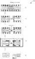
- FIG. 1illustrates a method of building conductive Through-Hole-Vias in glass substrates in accordance with an example.
- FIG. 2illustrates a method of building a Through-Hole-Via in glass substrates in accordance with an example.
- FIG. 3illustrates a method of building a Through-Hole-Via in glass substrates in accordance with an example.
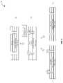
- FIG. 4illustrates a method of adding a conductor to a Through-Hole-Via in glass substrates in accordance with an example.
- FIG. 5illustrates a method of adding a conductor to a Through-Hole-Via in glass substrates in accordance with an example.
- FIG. 6illustrates a method of adding a conductor to a Through-Hole-Via in glass substrates in accordance with an example.
- an example embodimentforms THV or conductive THV after the circuitry has been placed onto the glass substrate.
- FIG. 1illustrates a method 100 of building conductive Through-Hole-Vias in glass substrates in accordance with an example.
- circuit layoutis designed with identified THV locations over glass substrate.
- protective film/coatingis applied over circuitry.
- an opening in film/covering over THV locations with circuitry enclosed by the film/coatingis formed.
- the THV locationis designed to avoid any effect on Thin Film Transistor (TFT) circuitry during the THV formation process.
- TFTThin Film Transistor
- the THV locationcan have no circuitry and is in a safe distance from the circuitry.
- the THV formation processmay have heat generated that could affect the performance of the circuitry.
- THV in the substrate at the locationsis formed.
- conductive materials in the THVsare formed.
- the THV and circuitryare electrically connected with conductive material between THV and designated circuit contact point.
- the substratecan be used to form LED or OLED over the circuitry (e.g., active matrix), and form driver circuitry and/or flexible printed circuits (FPCs) over the back of the substrate for a display module.
- the substratecan also be used as glass interposer and for 3D packaging where multiple devices such as semiconductor chips can be mounted on both top and bottom sides of the substrate and electrically connected by the THV.
- FIG. 2illustrates a method 200 of building a Through-Hole-Via in glass substrates in accordance with an example.
- protective film/coatingis applied over both circuitry and glass substrate.
- the protective coatingcan be photoresist that can be patterned by photolithographic method or can be an acid-resist film patterned by laser drill holes in the film.
- holes in protective coatingare opened at the designated TGV location. This can be done by photolithography or by laser beam irradiation.
- the film openingis laser irradiated (e.g., via laser induced deep etching (LIDE)) to induce structural damage in glass at the designated locations.
- LIDElaser induced deep etching
- etching solutioncan be hydrofluoric acid (HF)-based for example.
- Protective coatingcan resist etching solution such that the etching rate of un-damaged glass area is much slower than damaged area.
- the protective filmis removed and the TGV substrate is ready for conductive material fill process as shown and described below in conjunction with FIG. 4 .
- FIG. 3illustrates a method 300 of building a Through-Hole-Via in glass substrates in accordance with an example.
- circuitryis located on first and second opposing sides of a glass substrate.
- protective film/coatingis applied on both sides of circuit and glass substrate.
- Protective coatingcan be photoresist that can be patterned by photolithographic method or can be an acid-resist film patterned by laser drill holes in the film.
- holesare opened in protective coating at the designated TGV location. This can be done by photolithography or by laser beam irradiation.
- laser radiationis radiated onto the film opening and induce structural damage in glass at the designated locations (e.g., via LIDE).
- etching solutioncan be HF-based.
- Protective coatingcan be resistant to etching solution such that the etching rate of undamaged glass area is slower than damaged area.
- protective filmis removed and the TGV substrate is ready for conductive material fill process, e.g., FIG. 4 , etc.
- FIG. 4illustrates a method 400 of adding a conductor to a Through-Hole-Via in glass substrates in accordance with an example.
- filler stopis applied over all the TGV on circuit side.
- Filler stopcan a temporary layer of solid film such as polyimide (PI).
- PIpolyimide
- conductive paste/inkis filled in the via under vacuum.
- the fill methodcan be screen printing or inject printing, etc. Vacuum prevents air in the via that could prevent the filler material from going into the via.
- the amount and shape of the excess paste/inksometimes is not easy to control. It maybe necessary to have the excess removed and use the well defined solder paste screen printing process to create well defined connection to the circuitry.
- solder stopis removed.
- Solderis screen printed and reflowed to electrically connect the filled TGV to the circuitry (e.g., TFT circuitry such as active matrix or passive matrix for displays).
- Conductive paste/ink materialcan be epoxy based Cu or Ag paste; or solder paste such as SnAg. When epoxy based is used, the paste/ink usually require oven bake to cure. If solder paste is used, a high temperature re-flow (200-400 degrees C.) is required to form joints.
- FIG. 5illustrates a method 500 of adding a conductor to a Through-Hole-Via in glass substrates in accordance with an example.
- filler stopis applied on one side of the glass substrate and masking the other side over the circuitry with openings larger than the TGV to expose the circuit contact points that need to be connected to the TGV.
- conductive paste/inkis vacuum screen printed so that it covers the exposed circuit contact points.
- C and Dafter paste/ink is cured the mask is removed. Note the paste print over the mask could break off as shown in C, or can break off at the substrate surface level as shown in D.
- FIG. 6illustrates a method 600 of adding a conductor to a Through-Hole-Via in glass substrates in accordance with an example.
- a protective coatingis formed on both sides of the circuit-glass substrate with TGV.
- openingsare formed over the TGV area to expose part of the circuitry to be connected.
- conductive coatingis formed to electrically connect circuitry on both sides of the glass substrate.
- the protective coatingis removed.
- the conductive materialcan be metal, Indium tin oxide (ITO), conductive paste/ink.
- Metal coatingcan be formed by electroplating or electroless plating. Conductive paste/ink can be applied by screen printing such that the TGV can be completely filled or partially filled.
- a method for forming a conductive through-hole-via in a glass substratecomprising:
- circuitryon a first surface of the glass substrate such that a section of the glass substrate on the first surface is exposed; applying a coating to the first surface covering both the circuitry and the exposed section of the first surface; removing the coating over the exposed section; inducing structural damage to at least a portion of the exposed section with laser radiation; and wet etching away the at least a portion of the exposed section to form a via.
- filler stopon the first surface; in a vacuum, filling the via with a conductor; and curing the conductor.
- filler stopon the first surface; in a vacuum, filling the via with a conductor; curing the conductor; removing the filler stop; and electrically connecting the cured conductor in the via with the circuitry.
- applying the coatingincludes applying photoresist via photolithography.
- applying the coatingincludes applying an acid-resist film patterned by laser drill holes.
- circuitryincludes active matrix display circuitry.
- circuitryincludes passive matrix display circuitry.
- filler stopon a second surface of the substrate opposing the first surface; applying a mask over the circuitry leaving an exposed section of mask having a width greater than a width of the via; in a vacuum, filling the via with a conductor; vacuum screen printing the conductor over exposed circuit contact points of the circuitry; curing the conductor; and removing the filler stop.
- a glass substratecomprising:
Landscapes
- Engineering & Computer Science (AREA)
- Physics & Mathematics (AREA)
- Condensed Matter Physics & Semiconductors (AREA)
- General Physics & Mathematics (AREA)
- Computer Hardware Design (AREA)
- Microelectronics & Electronic Packaging (AREA)
- Power Engineering (AREA)
- Manufacturing & Machinery (AREA)
- Ceramic Engineering (AREA)
- Chemical & Material Sciences (AREA)
- Optics & Photonics (AREA)
- General Chemical & Material Sciences (AREA)
- Inorganic Chemistry (AREA)
- Chemical Kinetics & Catalysis (AREA)
- Printing Elements For Providing Electric Connections Between Printed Circuits (AREA)
- Manufacturing Of Printed Circuit Boards (AREA)
Abstract
Description
- This application claims priority to and incorporates by reference U.S. Provisional Patent Application No. 63/209,902 filed Jun. 11, 2021.
- This disclosure related to vias and more particularly, but not exclusively, to building conductive vias in through glass substrates.
- Prefabricated vias on glass substrate (before placement of circuitry) may cause glass breakage or contamination to the tools used for the fabrication process. For example, glass with a Through-Hole Via (THV) may have residual stress that could lead to glass breakage during the mechanical transfer at or between process steps; metal in the conductive material used to fill the THV can be a source of contamination to the polysilicon (Low Temperature Polycrystal Silicon (LTPS)) or amorphous silicon Thin Film Transistor (TFT) during the deposition of these materials.
- A method for forming a conductive through-hole-via in a glass substrate comprises: placing circuitry on a first surface of the glass substrate such that a section of the glass substrate on the first surface is exposed; applying a coating to the first surface covering both the circuitry and the exposed section of the first surface; removing the coating over the exposed section; inducing structural damage to at least a portion of the exposed section with laser radiation; and wet etching away the at least a portion of the exposed section to form a via.
- To easily identify the discussion of any particular element or act, the most significant digit or digits in a reference number refer to the figure number in which that element is first introduced.
FIG.1 illustrates a method of building conductive Through-Hole-Vias in glass substrates in accordance with an example.FIG.2 illustrates a method of building a Through-Hole-Via in glass substrates in accordance with an example.FIG.3 illustrates a method of building a Through-Hole-Via in glass substrates in accordance with an example.FIG.4 illustrates a method of adding a conductor to a Through-Hole-Via in glass substrates in accordance with an example.FIG.5 illustrates a method of adding a conductor to a Through-Hole-Via in glass substrates in accordance with an example.FIG.6 illustrates a method of adding a conductor to a Through-Hole-Via in glass substrates in accordance with an example.- In order to mitigate manufacturing issues in glass substrates, an example embodiment forms THV or conductive THV after the circuitry has been placed onto the glass substrate.
FIG.1 illustrates amethod 100 of building conductive Through-Hole-Vias in glass substrates in accordance with an example. Inblock 102, circuit layout is designed with identified THV locations over glass substrate. Inblock 104, protective film/coating is applied over circuitry. Inblock 106, an opening in film/covering over THV locations with circuitry enclosed by the film/coating is formed. The THV location is designed to avoid any effect on Thin Film Transistor (TFT) circuitry during the THV formation process. For example, the THV location can have no circuitry and is in a safe distance from the circuitry. The THV formation process may have heat generated that could affect the performance of the circuitry. Inblock 108, THV in the substrate at the locations is formed. Inblock 110, conductive materials in the THVs are formed. Inblock 112, the THV and circuitry are electrically connected with conductive material between THV and designated circuit contact point.- The substrate can be used to form LED or OLED over the circuitry (e.g., active matrix), and form driver circuitry and/or flexible printed circuits (FPCs) over the back of the substrate for a display module. The substrate can also be used as glass interposer and for 3D packaging where multiple devices such as semiconductor chips can be mounted on both top and bottom sides of the substrate and electrically connected by the THV.
FIG.2 illustrates amethod 200 of building a Through-Hole-Via in glass substrates in accordance with an example. At A, protective film/coating is applied over both circuitry and glass substrate. The protective coating can be photoresist that can be patterned by photolithographic method or can be an acid-resist film patterned by laser drill holes in the film. Next, at B, holes in protective coating are opened at the designated TGV location. This can be done by photolithography or by laser beam irradiation. Next, at C, the film opening is laser irradiated (e.g., via laser induced deep etching (LIDE)) to induce structural damage in glass at the designated locations. At D, the damaged glass area is wet etched away in etching solution (can be hydrofluoric acid (HF)-based for example). Protective coating can resist etching solution such that the etching rate of un-damaged glass area is much slower than damaged area. At E, the protective film is removed and the TGV substrate is ready for conductive material fill process as shown and described below in conjunction withFIG.4 .FIG.3 illustrates amethod 300 of building a Through-Hole-Via in glass substrates in accordance with an example. In this example, circuitry is located on first and second opposing sides of a glass substrate. At A, protective film/coating is applied on both sides of circuit and glass substrate. Protective coating can be photoresist that can be patterned by photolithographic method or can be an acid-resist film patterned by laser drill holes in the film. At B, holes are opened in protective coating at the designated TGV location. This can be done by photolithography or by laser beam irradiation. Next, at C, laser radiation is radiated onto the film opening and induce structural damage in glass at the designated locations (e.g., via LIDE). Next, at D, damaged glass area is wet etched away in etching solution (can be HF-based). Protective coating can be resistant to etching solution such that the etching rate of undamaged glass area is slower than damaged area. At E, protective film is removed and the TGV substrate is ready for conductive material fill process, e.g.,FIG.4 , etc.FIG.4 illustrates amethod 400 of adding a conductor to a Through-Hole-Via in glass substrates in accordance with an example. Continuing from themethod 200, at A, filler stop is applied over all the TGV on circuit side. Filler stop can a temporary layer of solid film such as polyimide (PI). Next, at B, conductive paste/ink is filled in the via under vacuum. The fill method can be screen printing or inject printing, etc. Vacuum prevents air in the via that could prevent the filler material from going into the via. Optionally, at C, the amount and shape of the excess paste/ink sometimes is not easy to control. It maybe necessary to have the excess removed and use the well defined solder paste screen printing process to create well defined connection to the circuitry. Accordingly, after curing the paste/ink, excessive paste/ink extruding the substrate can be removed. At D, filler stop is removed. Solder is screen printed and reflowed to electrically connect the filled TGV to the circuitry (e.g., TFT circuitry such as active matrix or passive matrix for displays).- Conductive paste/ink material can be epoxy based Cu or Ag paste; or solder paste such as SnAg. When epoxy based is used, the paste/ink usually require oven bake to cure. If solder paste is used, a high temperature re-flow (200-400 degrees C.) is required to form joints.
FIG.5 illustrates amethod 500 of adding a conductor to a Through-Hole-Via in glass substrates in accordance with an example. Continuing from themethod 200, at A, filler stop is applied on one side of the glass substrate and masking the other side over the circuitry with openings larger than the TGV to expose the circuit contact points that need to be connected to the TGV. At B, conductive paste/ink is vacuum screen printed so that it covers the exposed circuit contact points. At C and D, after paste/ink is cured the mask is removed. Note the paste print over the mask could break off as shown in C, or can break off at the substrate surface level as shown in D.FIG.6 illustrates amethod 600 of adding a conductor to a Through-Hole-Via in glass substrates in accordance with an example. Continuing from themethod 300, at A, a protective coating is formed on both sides of the circuit-glass substrate with TGV. Next, at B, openings are formed over the TGV area to expose part of the circuitry to be connected. At C, conductive coating is formed to electrically connect circuitry on both sides of the glass substrate. At D, the protective coating is removed. The conductive material can be metal, Indium tin oxide (ITO), conductive paste/ink. Metal coating can be formed by electroplating or electroless plating. Conductive paste/ink can be applied by screen printing such that the TGV can be completely filled or partially filled.- In view of the disclosure above, various examples are set forth below. It should be noted that one or more features of an example, taken in isolation or combination, should be considered within the disclosure of this application.
- 1. A method for forming a conductive through-hole-via in a glass substrate, comprising:
- placing circuitry on a first surface of the glass substrate such that a section of the glass substrate on the first surface is exposed;
applying a coating to the first surface covering both the circuitry and the exposed section of the first surface;
removing the coating over the exposed section;
inducing structural damage to at least a portion of the exposed section with laser radiation; and wet etching away the at least a portion of the exposed section to form a via. - 2. The method of example 1, wherein the removing the coating over the exposed section is performed with photolithography or laser beam irradiation.
- 3. The method of any of the preceding examples, further comprising:
- placing second circuitry on a second surface of the glass substrate such that a second section of the glass substrate on the second surface is exposed, the second surface opposing the first surface; and
applying coating to the second surface covering both the second circuitry and the second exposed section of the second surface. - 4. The method of any of the preceding examples, further comprising:
- placing filler stop on the first surface;
in a vacuum, filling the via with a conductor; and
curing the conductor. - 5. The method of any of the preceding examples, wherein the conductive coating includes a metal plating and the applying the conductive coating includes electroplating or electroless plating.
- 6. The method of any of the preceding examples, wherein the conductive coating includes indium tin oxide.
- 7. The method of any of the preceding examples, wherein the conductive coating includes an epoxy based paste and the applying the conductive coating include vacuum screen printing.
- 8. The method of any of the preceding examples, further comprising;
- applying a second coating to the first and second surfaces;
forming openings in the via area exposing a portion of the first and second circuitry to be connected;
forming conductive coating to electrically connect first and second circuitries. - 9. The method of any of the preceding examples, further comprising:
- placing filler stop on the first surface;
in a vacuum, filling the via with a conductor;
curing the conductor;
removing the filler stop; and
electrically connecting the cured conductor in the via with the circuitry. - 10. The method any of the preceding examples, further comprising removing excess conductor that extends out of the substrate.
- 11. The method of any of the preceding examples, wherein the conductor includes an epoxy-based paste.
- 12. The method of any of the preceding examples, wherein the conductor includes a solder paste.
- 13. The method of any of the preceding examples, wherein the applying the coating includes applying photoresist via photolithography.
- 14. The method of any of the preceding examples, wherein the applying the coating includes applying an acid-resist film patterned by laser drill holes.
- 15. The method of any of the preceding examples, wherein the wet etching uses hydrofluoric acid and the coating is resistant to the acid.
- 16. The method of any of the preceding examples, wherein the circuitry includes active matrix display circuitry.
- 17. The method of any of the preceding examples, wherein the circuitry includes passive matrix display circuitry.
- 18. The method any of the preceding examples, further comprising:
- placing filler stop on a second surface of the substrate opposing the first surface;
applying a mask over the circuitry leaving an exposed section of mask having a width greater than a width of the via;
in a vacuum, filling the via with a conductor;
vacuum screen printing the conductor over exposed circuit contact points of the circuitry;
curing the conductor; and
removing the filler stop. - 19. The method of any of the preceding examples, further comprising removing any remaining coating.
- 20. A glass substrate, comprising:
- a first circuitry on a first surface and a second circuitry on a second surface;
the second surface opposing the first surface;
at least one through-glass-via electrically connecting the first and second circuitry;
wherein the at least one through-glass-via is made after the circuitries are made over the glass substrate per any of the preceding examples.
Claims (20)
Priority Applications (1)
| Application Number | Priority Date | Filing Date | Title |
|---|---|---|---|
| US17/724,317US20220399206A1 (en) | 2021-06-11 | 2022-04-19 | Method for building conductive through-hole vias in glass substrates |
Applications Claiming Priority (2)
| Application Number | Priority Date | Filing Date | Title |
|---|---|---|---|
| US202163209902P | 2021-06-11 | 2021-06-11 | |
| US17/724,317US20220399206A1 (en) | 2021-06-11 | 2022-04-19 | Method for building conductive through-hole vias in glass substrates |
Publications (1)
| Publication Number | Publication Date |
|---|---|
| US20220399206A1true US20220399206A1 (en) | 2022-12-15 |
Family
ID=83160512
Family Applications (1)
| Application Number | Title | Priority Date | Filing Date |
|---|---|---|---|
| US17/724,317AbandonedUS20220399206A1 (en) | 2021-06-11 | 2022-04-19 | Method for building conductive through-hole vias in glass substrates |
Country Status (3)
| Country | Link |
|---|---|
| US (1) | US20220399206A1 (en) |
| CN (1) | CN115050652A (en) |
| TW (1) | TWI845961B (en) |
Cited By (1)
| Publication number | Priority date | Publication date | Assignee | Title |
|---|---|---|---|---|
| RU2803557C1 (en)* | 2023-05-05 | 2023-09-15 | Федеральное государственное унитарное предприятие "Центральный научно-исследовательский институт химии и механики" (ФГУП "ЦНИИХМ") | Method for forming through holes in glass plates |
Families Citing this family (2)
| Publication number | Priority date | Publication date | Assignee | Title |
|---|---|---|---|---|
| CN116209161A (en)* | 2023-03-14 | 2023-06-02 | 深圳市纽菲斯新材料科技有限公司 | Glass-based circuit component and preparation method and application thereof |
| CN119581412A (en)* | 2024-12-06 | 2025-03-07 | 苏州森丸电子技术有限公司 | TGV processing filling method |
Citations (5)
| Publication number | Priority date | Publication date | Assignee | Title |
|---|---|---|---|---|
| US5367764A (en)* | 1991-12-31 | 1994-11-29 | Tessera, Inc. | Method of making a multi-layer circuit assembly |
| US20070019141A1 (en)* | 2004-12-28 | 2007-01-25 | Yuko Kizu | Liquid crystal display |
| US20070281247A1 (en)* | 2006-05-30 | 2007-12-06 | Phillips Scott E | Laser ablation resist |
| US20180324958A1 (en)* | 2015-11-06 | 2018-11-08 | Richview Electronics Co., Ltd. | Single-layer circuit board, multi-layer circuit board, and manufacturing methods therefor |
| US20200321301A1 (en)* | 2017-10-11 | 2020-10-08 | Sony Semiconductor Solutions Corporation | Semiconductor device and method of manufacturing the same |
Family Cites Families (6)
| Publication number | Priority date | Publication date | Assignee | Title |
|---|---|---|---|---|
| JP4702794B2 (en)* | 2003-10-06 | 2011-06-15 | Hoya株式会社 | Method for forming through hole in photosensitive glass substrate |
| TWI528880B (en)* | 2012-06-27 | 2016-04-01 | 欣興電子股份有限公司 | Method for forming conductive through via at glass substrate |
| WO2017034969A1 (en)* | 2015-08-21 | 2017-03-02 | Corning Incorporated | Methods of continuous fabrication of features in flexible substrate webs and products relating to the same |
| TW202224211A (en)* | 2016-03-31 | 2022-06-16 | 美商伊雷克托科學工業股份有限公司 | Methods of laser-seeding for electro-conductive plating |
| US20200294728A1 (en)* | 2017-10-04 | 2020-09-17 | Alliance For Sustainable Energy, Llc | Perovskite devices and methods of making the same |
| US11654657B2 (en)* | 2017-10-27 | 2023-05-23 | Corning Incorporated | Through glass via fabrication using a protective material |
- 2022
- 2022-04-19USUS17/724,317patent/US20220399206A1/ennot_activeAbandoned
- 2022-06-08TWTW111121238Apatent/TWI845961B/enactive
- 2022-06-09CNCN202210643955.3Apatent/CN115050652A/enactivePending
Patent Citations (5)
| Publication number | Priority date | Publication date | Assignee | Title |
|---|---|---|---|---|
| US5367764A (en)* | 1991-12-31 | 1994-11-29 | Tessera, Inc. | Method of making a multi-layer circuit assembly |
| US20070019141A1 (en)* | 2004-12-28 | 2007-01-25 | Yuko Kizu | Liquid crystal display |
| US20070281247A1 (en)* | 2006-05-30 | 2007-12-06 | Phillips Scott E | Laser ablation resist |
| US20180324958A1 (en)* | 2015-11-06 | 2018-11-08 | Richview Electronics Co., Ltd. | Single-layer circuit board, multi-layer circuit board, and manufacturing methods therefor |
| US20200321301A1 (en)* | 2017-10-11 | 2020-10-08 | Sony Semiconductor Solutions Corporation | Semiconductor device and method of manufacturing the same |
Cited By (1)
| Publication number | Priority date | Publication date | Assignee | Title |
|---|---|---|---|---|
| RU2803557C1 (en)* | 2023-05-05 | 2023-09-15 | Федеральное государственное унитарное предприятие "Центральный научно-исследовательский институт химии и механики" (ФГУП "ЦНИИХМ") | Method for forming through holes in glass plates |
Also Published As
| Publication number | Publication date |
|---|---|
| CN115050652A (en) | 2022-09-13 |
| TW202249545A (en) | 2022-12-16 |
| TWI845961B (en) | 2024-06-21 |
Similar Documents
| Publication | Publication Date | Title |
|---|---|---|
| US10418331B2 (en) | Interconnection structures and methods for transfer-printed integrated circuit elements with improved interconnection alignment tolerance | |
| US10085347B2 (en) | Manufacture of a circuit board and circuit board containing a component | |
| US20220399206A1 (en) | Method for building conductive through-hole vias in glass substrates | |
| US7198989B2 (en) | Method of producing a COF flexible printed wiring board | |
| CN104428892B (en) | Method and apparatus for substrate core layer | |
| US20160322290A1 (en) | Substrate for integrated circuit devices including multi-layer glass core and methods of making the same | |
| KR20110002426A (en) | Manufacturing Method of Semiconductor Device | |
| US11483937B2 (en) | Methods of making printed structures | |
| JP5903920B2 (en) | Semiconductor device manufacturing method and electronic device manufacturing method | |
| CN109509727B (en) | Semiconductor chip packaging method and packaging structure | |
| US11916179B2 (en) | Structures and methods for electrically connecting printed horizontal components | |
| EP3975241B1 (en) | Method of producing circuit boards | |
| US20160143139A1 (en) | Electronic component device and method for manufacturing the same | |
| CN111584507A (en) | Display panel, manufacturing method thereof and display terminal | |
| US20250316639A1 (en) | Semiconductor chip package having underfill material surrounding a fan-out package and contacting a stress buffer structure sidewall | |
| US20200077515A1 (en) | Printed circuit board | |
| US6808643B2 (en) | Hybrid interconnect substrate and method of manufacture thereof | |
| TWI643532B (en) | Circuit board structure and method for fabricating the same | |
| US20050205972A1 (en) | COF flexible printed wiring board and semiconductor device | |
| CN1180461C (en) | Composite high-density packaging substrate and forming method thereof | |
| CN112243317B (en) | Circuit board structure and manufacturing method thereof | |
| JP7226973B2 (en) | Substrate for forming via wiring, method for manufacturing substrate for forming via wiring, and method for mounting semiconductor chip | |
| CN120021014A (en) | A packaging structure and a method for preparing the same | |
| JP2025035919A (en) | Method for manufacturing conductive laminated glass composite | |
| CN2550902Y (en) | Packaging modules for semiconductor components |
Legal Events
| Date | Code | Title | Description |
|---|---|---|---|
| AS | Assignment | Owner name:V-FINITY INC., CALIFORNIA Free format text:ASSIGNMENT OF ASSIGNORS INTEREST;ASSIGNOR:LIU, HENG;REEL/FRAME:059642/0063 Effective date:20220419 | |
| STPP | Information on status: patent application and granting procedure in general | Free format text:DOCKETED NEW CASE - READY FOR EXAMINATION | |
| AS | Assignment | Owner name:V-FINITY INC., CALIFORNIA Free format text:ASSIGNMENT OF ASSIGNORS INTEREST;ASSIGNOR:V-FINITY INTERNATIONAL;REEL/FRAME:060102/0130 Effective date:20220517 | |
| AS | Assignment | Owner name:V-FINITY, INC., CALIFORNIA Free format text:CORRECTIVE ASSIGNMENT TO CORRECT THE APPLICATION NUMBER 60901144 PREVIOUSLY RECORDED AT REEL: 060102 FRAME: 0130. ASSIGNOR(S) HEREBY CONFIRMS THE ASSIGNMENT;ASSIGNOR:V-FINITY INTERNATIONAL;REEL/FRAME:060455/0629 Effective date:20220517 | |
| STPP | Information on status: patent application and granting procedure in general | Free format text:NON FINAL ACTION MAILED | |
| STPP | Information on status: patent application and granting procedure in general | Free format text:RESPONSE TO NON-FINAL OFFICE ACTION ENTERED AND FORWARDED TO EXAMINER | |
| STPP | Information on status: patent application and granting procedure in general | Free format text:NON FINAL ACTION MAILED | |
| STCB | Information on status: application discontinuation | Free format text:ABANDONED -- FAILURE TO RESPOND TO AN OFFICE ACTION |