US20220208590A1 - Semiconductor processing apparatus and method - Google Patents
Semiconductor processing apparatus and methodDownload PDFInfo
- Publication number
- US20220208590A1 US20220208590A1US17/520,052US202117520052AUS2022208590A1US 20220208590 A1US20220208590 A1US 20220208590A1US 202117520052 AUS202117520052 AUS 202117520052AUS 2022208590 A1US2022208590 A1US 2022208590A1
- Authority
- US
- United States
- Prior art keywords
- processing apparatus
- semiconductor processing
- wafer
- radio frequency
- pass filter
- Prior art date
- Legal status (The legal status is an assumption and is not a legal conclusion. Google has not performed a legal analysis and makes no representation as to the accuracy of the status listed.)
- Granted
Links
Images


Classifications
- H—ELECTRICITY
- H01—ELECTRIC ELEMENTS
- H01J—ELECTRIC DISCHARGE TUBES OR DISCHARGE LAMPS
- H01J37/00—Discharge tubes with provision for introducing objects or material to be exposed to the discharge, e.g. for the purpose of examination or processing thereof
- H01J37/32—Gas-filled discharge tubes
- H01J37/32431—Constructional details of the reactor
- H01J37/32532—Electrodes
- H01J37/32568—Relative arrangement or disposition of electrodes; moving means
- H—ELECTRICITY
- H01—ELECTRIC ELEMENTS
- H01J—ELECTRIC DISCHARGE TUBES OR DISCHARGE LAMPS
- H01J37/00—Discharge tubes with provision for introducing objects or material to be exposed to the discharge, e.g. for the purpose of examination or processing thereof
- H01J37/32—Gas-filled discharge tubes
- H01J37/32431—Constructional details of the reactor
- H01J37/32715—Workpiece holder
- H—ELECTRICITY
- H01—ELECTRIC ELEMENTS
- H01J—ELECTRIC DISCHARGE TUBES OR DISCHARGE LAMPS
- H01J37/00—Discharge tubes with provision for introducing objects or material to be exposed to the discharge, e.g. for the purpose of examination or processing thereof
- H01J37/32—Gas-filled discharge tubes
- H01J37/32009—Arrangements for generation of plasma specially adapted for examination or treatment of objects, e.g. plasma sources
- H01J37/32082—Radio frequency generated discharge
- H01J37/32174—Circuits specially adapted for controlling the RF discharge
- H01J37/32183—Matching circuits
- H—ELECTRICITY
- H01—ELECTRIC ELEMENTS
- H01L—SEMICONDUCTOR DEVICES NOT COVERED BY CLASS H10
- H01L21/00—Processes or apparatus adapted for the manufacture or treatment of semiconductor or solid state devices or of parts thereof
- H01L21/67—Apparatus specially adapted for handling semiconductor or electric solid state devices during manufacture or treatment thereof; Apparatus specially adapted for handling wafers during manufacture or treatment of semiconductor or electric solid state devices or components ; Apparatus not specifically provided for elsewhere
- H01L21/683—Apparatus specially adapted for handling semiconductor or electric solid state devices during manufacture or treatment thereof; Apparatus specially adapted for handling wafers during manufacture or treatment of semiconductor or electric solid state devices or components ; Apparatus not specifically provided for elsewhere for supporting or gripping
- H01L21/6831—Apparatus specially adapted for handling semiconductor or electric solid state devices during manufacture or treatment thereof; Apparatus specially adapted for handling wafers during manufacture or treatment of semiconductor or electric solid state devices or components ; Apparatus not specifically provided for elsewhere for supporting or gripping using electrostatic chucks
- H01L21/6833—Details of electrostatic chucks
- H—ELECTRICITY
- H01—ELECTRIC ELEMENTS
- H01J—ELECTRIC DISCHARGE TUBES OR DISCHARGE LAMPS
- H01J2237/00—Discharge tubes exposing object to beam, e.g. for analysis treatment, etching, imaging
- H01J2237/20—Positioning, supporting, modifying or maintaining the physical state of objects being observed or treated
- H01J2237/2007—Holding mechanisms
- H—ELECTRICITY
- H01—ELECTRIC ELEMENTS
- H01J—ELECTRIC DISCHARGE TUBES OR DISCHARGE LAMPS
- H01J2237/00—Discharge tubes exposing object to beam, e.g. for analysis treatment, etching, imaging
- H01J2237/32—Processing objects by plasma generation
- H01J2237/33—Processing objects by plasma generation characterised by the type of processing
- H01J2237/332—Coating
- H01J2237/3321—CVD [Chemical Vapor Deposition]
Definitions
- This applicationgenerally relates to the field of semiconductor manufacturing apparatuses, and more specifically, to a semiconductor processing apparatus and method.
- a semiconductor processing apparatusgenerally includes an electrostatic chuck.
- the electrostatic chuckis an ultra-clean wafer carrier applicable to vacuum and plasma operating conditions, and is used for clamping a wafer in a smooth and uniform manner by using an electrostatic adsorption principle.
- the electrostatic chuckis often used for maintaining the temperature and warpage of the wafer, and is a core component of semiconductor processing apparatuses such as a plasma-enhanced chemical vapor deposition apparatus and an ion implantation apparatus.
- a direct currentneeds to pass through a direct-current power supply, a surface of a wafer pocket, plasma, and a ground to form a direct current loop.
- a material commonly used for side walls of a process chamber in contact with the plasmais ceramic, which is adverse to free conduction of charges in the plasma, and thus a stable and effective direct current channel from the plasma to the ground cannot be provided.
- an upper electrode in contact with the plasmais usually used as an electrode to which radio frequency is applied, and is coupled with a matching circuit.
- Solutions of this applicationcan provide an effective direct current loop to an electrostatic chuck in a semiconductor processing apparatus, to enhance stability of a direct current, improve electrostatic absorption and release functions, and improve process stability and production efficiency of the semiconductor processing apparatus.
- this applicationprovides a semiconductor processing apparatus, including: a wafer pocket provided with a lower electrode, where the lower electrode is coupled to a direct-current power supply; and an upper electrode disposed opposite to the wafer pocket, where the upper electrode is coupled to a radio frequency generator through a matching circuit, and is grounded through a low-pass filter.
- the low-pass filtermay include a resistor and an inductor.
- a resistance value of the resistoris fixed or adjustable.
- the resistance value or a resistance value range of the resistoris selected based on requirements of a leakage current on a surface of the wafer pocket.
- the low-pass filtermay be connected to a radio frequency feed conductor between the upper electrode and the matching circuit.
- the low-pass filtermay be grounded through a shielding cover plate.
- the low-pass filtermay be disposed in the matching circuit.
- the low-pass filtermay include a direct-current leakage current channel in the matching circuit.
- the low-pass filtermay include a metal-doped ceramic chip capacitor in the matching circuit.
- the wafer pocketmay be made of an insulating material.
- the wafer pocketincludes a J-R type electrostatic chuck.
- the semiconductor processing apparatusmay include a plasma-enhanced chemical vapor deposition apparatus.
- this applicationfurther provides a method of using the semiconductor processing apparatus described in any embodiment of this application, including: placing a wafer on the wafer pocket; and applying a voltage to the lower electrode in the wafer pocket by the direct-current power supply, to absorb the wafer on a surface of the wafer pocket.
- the methodmay further include: applying, during a period in which the voltage is applied to the lower electrode, a radio frequency power to the upper electrode by the radio frequency generator, to generate plasma between the upper electrode and the wafer.
- the methodmay further include: stopping applying the voltage to the lower electrode, to release the wafer from the surface of the wafer pocket.
- the methodmay further include: applying, during a period in which no voltage is applied to the lower electrode, a radio frequency power to the upper electrode by the radio frequency generator, to generate plasma between the upper electrode and the wafer.
- FIG. 1is a schematic structural diagram of a semiconductor processing apparatus according to some embodiments of this application.
- FIG. 2is a schematic structural diagram of another semiconductor processing apparatus according to some embodiments of this application.
- FIG. 3is a schematic structural diagram of another semiconductor processing apparatus according to some embodiments of this application.
- connectionshould be construed as including “direct connection” and “connection through one or more intermediate components.”
- the names of the various components used in this specificationare only for illustrative purposes, but are not limitative. Different manufacturers may use different names to refer to components with the same function.
- FIG. 1is a schematic structural diagram of a semiconductor processing apparatus 10 according to some embodiments of this application.
- the semiconductor processing apparatus 10includes a plasma-enhanced chemical vapor deposition apparatus.
- the semiconductor processing apparatus 10may include a wafer pocket 101 , a lower electrode 102 , an upper electrode 103 , a low-pass filter 104 , a matching circuit 105 , a radio frequency generator 106 and a direct-current power supply 107 .
- the wafer pocket 101is disposed in a process chamber defined by side walls 111 , and is fixed on a supporter 109 .
- the lower electrode 102is disposed in the wafer pocket 101 , and is coupled to the direct-current power supply 107 .
- a filter 108is disposed between the direct-current power supply 107 and the lower electrode 102 .
- a direct currentmay flow to the lower electrode 102 through the filter 108
- a radio frequency currentmay flow to a ground through the filter 108 .
- the upper electrode 103is disposed above the wafer pocket 101 and is opposite to the wafer pocket 101 .
- the upper electrode 103is coupled to the radio frequency generator 106 through the matching circuit 105 .
- the radio frequency generator 106may provide a radio frequency power to the upper electrode 103 .
- Process gas in the process chambergenerates glow discharge under an action of a radio frequency electric field of the upper electrode 103 , to form plasma 113 , and is finally deposited on a surface of a wafer 112 placed on the wafer pocket 101 to form a solid film. As shown by the dashed-line arrows in FIG.
- the radio frequency currentmay flow from the radio frequency generator 106 , and finally flow to the ground through the matching circuit 105 , the upper electrode 103 , the plasma 113 , the wafer 112 , the wafer pocket 101 , the lower electrode 102 and the filter 108 , to form a radio frequency loop 114 .
- the upper electrode 103is further grounded through the low-pass filter 104 .
- the low-pass filter 104may include elements such as a resistor and an inductor.
- the direct currentmay flow to the ground through the low-pass filter 104 , and the low-pass filter 104 has high impedance against the radio frequency current.
- the direct-current power supply 107may apply a voltage to the lower electrode 102 , so that the lower electrode 102 is electrically biased with respect to the wafer pocket 101 , and polarized charges (and free charges) are generated on the surface of the wafer pocket 101 .
- the charges accumulated on the surface of the wafer pocket 101may further affect the wafer 112 , so that polarized charges are generated on a surface of the wafer 112 .
- the direct currentmay flow from the direct-current power supply 107 , and finally flow to the ground through the filter 108 , the lower electrode 102 , the wafer pocket 101 , the wafer 112 , the plasma 113 , the upper electrode 103 and the low-pass filter 104 , to form a direct current loop 115 .
- the direct current loop 115may provide a stable direct current, thereby improving stability of the electrostatic adsorption and electrostatic force.
- the direct current in the direct current loop 115is usually in a range of dozens of milliamperes (mA), and the radio frequency current in the radio frequency loop 114 is in a range of several amperes (A) to dozens of amperes (A). Therefore, the direct current has little effect on the plasma and can isolate the radio frequency.
- the direct-current power supply 107stops applying the voltage to the lower electrode 102 , there are residual charges on the surfaces of the wafer pocket 101 and the wafer 112 .
- the residual chargesmay be led out through the low-pass filter 104 , to release the wafer 112 from the surface of the wafer pocket 101 .
- the radio frequency generator 106may continue to apply the radio frequency power to the upper electrode 103 to generate the plasma 113 between the upper electrode 103 and the wafer 112 , but the process gas is removed and deposition is stopped.
- the radio frequency generator 106is turned off after the process is completed, and then the radio frequency generator 106 is turned on again, or the radio frequency generator 106 is not turned off after the process is completed.
- the radio frequency power provided during this periodmay be lower than that during a normal process, to prevent the plasma at relatively high self-bias from affecting the removal of charges.
- the low-pass filter 104provides a stable and good direct current loop, thereby improving repeatability and stability of the release.
- the wafer pocket 101may be a J-R type electrostatic chuck.
- the J-R type electrostatic chuckhas a larger adsorption force (which, for example, may be several orders of magnitude greater than an adsorption force of the Coulomb electrostatic chuck), so that the electrostatic adsorption effect is better.
- the wafer pocket 101may be made of an insulating material.
- the insulating materialincludes a ceramic material.
- the wafer pocket 101may further include a heater for performing thermal treatment on the wafer 112 .
- the lower electrode 102is sintered in the wafer pocket 101 .
- the radio frequency current generated by the radio frequency generator 106is a low frequency current, for example, a current with a frequency of 400 kHz. In some embodiments, the radio frequency current generated by the radio frequency generator 106 is a high frequency current, for example, a current with a frequency of 13.56 MHz. In some embodiments, the radio frequency current generated by the radio frequency generator 106 is a current with another frequency. In some embodiments, the radio frequency generator 106 may simultaneously provide both a low frequency current and a high frequency current. The low-pass filter 104 has high impedance against the radio frequency currents.
- the matching circuit 105may include an inductor and a capacitor. In some embodiments, the matching circuit 105 may include an inductor and two capacitors, where one of the capacitors is grounded. In some embodiments, the matching circuit 105 may include a ceramic chip capacitor.
- a resistance value of a resistor in the low-pass filter 104is fixed. In some other embodiments, a resistance value of a resistor in the low-pass filter 104 is adjustable, that is, the resistor has a specific resistance value range.
- the resistance value or resistance value range of the resistor in the low-pass filter 104is selected based on requirements of a leakage current on the surface of the wafer pocket 101 , to provide a suitable direct current to control a value and stability of the electrostatic adsorption force. For example, when the temperature of the process chamber is about 400° C., the leakage current on the surface of the wafer pocket 101 is less than 1 mA. Therefore, a current channel of 1 mA level may ensure stable operation of the electrostatic chuck.
- An electrostatic currentmay be limited by increasing the resistance value of the resistor in the low-pass filter 104 .
- FIG. 2is a schematic structural diagram of another semiconductor processing apparatus 20 according to some embodiments of this application.
- the semiconductor processing apparatus 20may include a radio frequency generator 206 , a matching circuit 205 , an upper electrode 203 and a wafer pocket 201 .
- a shielding cover plate 218is covered above the upper electrode 203 , to provide a ground for the semiconductor processing apparatus 20 .
- the matching circuit 205is connected to the upper electrode 203 through a radio frequency feed conductor 217 , and provides a matched radio frequency signal for the upper electrode 203 .
- the radio frequency feed conductor 217includes a copper tape or a copper pillar.
- the low-pass filter 204is connected to the radio frequency feed conductor 217 , and is grounded through the shielding cover plate 218 , thereby providing a stable direct current loop for electrostatic absorption and release.
- the low-pass filter 204is exemplarily shown as a resistor 2041 and an inductor 2042 connected in series.
- the low-pass filter 204may alternatively be implemented in other forms.
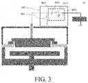
- FIG. 3is a schematic structural diagram of another semiconductor processing apparatus 30 according to some embodiments of this application.
- a structure of the semiconductor processing apparatus 30 and that of the semiconductor processing apparatus 20are basically the same, except that a low-pass filter 304 in the semiconductor processing apparatus 30 is disposed in a matching circuit 305 .
- Structures of the low-pass filter 304 and the matching circuit 305 shown in FIG. 3are only for illustrative purposes, and it should be understood that other circuit structures with similar functions do not depart from the spirit and scope of this application.
- the low-pass filter 304may be an additional low-pass filter circuit added to the matching circuit 305 .
- the low-pass filter 304may be an additional low-pass filter circuit, which is added outside a matching network 3051 , in the matching circuit 305 .
- the matching network 3051may include a network formed by a capacitor 3052 , a capacitor 3054 and an inductor 3053 .
- the low-pass filter circuitmay include a resistor and an inductor connected in series.
- the low-pass filter 304may include a direct-current leakage current channel in the matching circuit 305 .
- a matching network component in the matching circuit 305may include a ceramic chip capacitor.
- a milliampere-level leakage currentmay be formed, thereby forming the direct-current leakage current channel, and providing the direct current loop for electrostatic absorption and release.
- the milliampere-level leakage current in the matching circuit 305does not affect radio frequency applications and process performance of the matching circuit.
- a method of using the semiconductor processing apparatusmay include: placing a wafer on the wafer pocket; and applying a voltage to the lower electrode through the direct-current power supply, so that the wafer is absorbed to the surface of the wafer pocket.
- the methodmay further include: applying, during a period in which the voltage is applied to the lower electrode, a radio frequency power to the upper electrode by the radio frequency generator, to generate plasma between the upper electrode and the wafer.
- the methodmay further include: stopping applying the voltage to the lower electrode, to release the wafer from the surface of the wafer pocket.
- the methodmay further include: applying, during a period in which no voltage is applied to the lower electrode, a radio frequency power to the upper electrode by the radio frequency generator, to generate plasma between the upper electrode and the wafer.
- the semiconductor processing apparatusmay form a stable direct current loop through a grounded low-pass filter, resolving a technical problem that a stable direct current loop cannot be formed in the conventional semiconductor processing apparatus because electric charges cannot be led out from ceramic side walls, thereby increasing stability of the direct current loop in a process chamber, improving electrostatic absorption and release functions, and improving stability and efficiency of a deposition process.
Landscapes
- Engineering & Computer Science (AREA)
- Physics & Mathematics (AREA)
- Plasma & Fusion (AREA)
- Chemical & Material Sciences (AREA)
- Analytical Chemistry (AREA)
- General Physics & Mathematics (AREA)
- Condensed Matter Physics & Semiconductors (AREA)
- Manufacturing & Machinery (AREA)
- Computer Hardware Design (AREA)
- Microelectronics & Electronic Packaging (AREA)
- Power Engineering (AREA)
- Container, Conveyance, Adherence, Positioning, Of Wafer (AREA)
- Drying Of Semiconductors (AREA)
- Plasma Technology (AREA)
Abstract
Description
- This application claims priority to Chinese Patent Application No. 202011642968.6 filed on Dec. 31, 2020, and all the benefits accruing therefrom under 35 U.S.C. § 119, the contents of which in its entirety are herein incorporated by reference.
- This application generally relates to the field of semiconductor manufacturing apparatuses, and more specifically, to a semiconductor processing apparatus and method.
- A semiconductor processing apparatus generally includes an electrostatic chuck. The electrostatic chuck is an ultra-clean wafer carrier applicable to vacuum and plasma operating conditions, and is used for clamping a wafer in a smooth and uniform manner by using an electrostatic adsorption principle. In a semiconductor manufacturing process, the electrostatic chuck is often used for maintaining the temperature and warpage of the wafer, and is a core component of semiconductor processing apparatuses such as a plasma-enhanced chemical vapor deposition apparatus and an ion implantation apparatus.
- For a unipolar electrostatic chuck, during absorption and release, a direct current needs to pass through a direct-current power supply, a surface of a wafer pocket, plasma, and a ground to form a direct current loop. However, because a material commonly used for side walls of a process chamber in contact with the plasma is ceramic, which is adverse to free conduction of charges in the plasma, and thus a stable and effective direct current channel from the plasma to the ground cannot be provided. Moreover, an upper electrode in contact with the plasma is usually used as an electrode to which radio frequency is applied, and is coupled with a matching circuit. Because capacitance isolation exists between the upper electrode and the ground, a current in the direct current loop is blocked, which affects stability of the direct current, thus affecting an electrostatic absorption and release effect. The electrostatic absorption and release effect of the electrostatic chuck further affects process stability and production efficiency of the semiconductor processing apparatus.
- Solutions of this application can provide an effective direct current loop to an electrostatic chuck in a semiconductor processing apparatus, to enhance stability of a direct current, improve electrostatic absorption and release functions, and improve process stability and production efficiency of the semiconductor processing apparatus.
- In an aspect, this application provides a semiconductor processing apparatus, including: a wafer pocket provided with a lower electrode, where the lower electrode is coupled to a direct-current power supply; and an upper electrode disposed opposite to the wafer pocket, where the upper electrode is coupled to a radio frequency generator through a matching circuit, and is grounded through a low-pass filter.
- According to an embodiment of this application, the low-pass filter may include a resistor and an inductor.
- According to an embodiment of this application, a resistance value of the resistor is fixed or adjustable.
- According to an embodiment of this application, the resistance value or a resistance value range of the resistor is selected based on requirements of a leakage current on a surface of the wafer pocket.
- According to an embodiment of this application, the low-pass filter may be connected to a radio frequency feed conductor between the upper electrode and the matching circuit.
- According to an embodiment of this application, the low-pass filter may be grounded through a shielding cover plate.
- According to an embodiment of this application, the low-pass filter may be disposed in the matching circuit.
- According to an embodiment of this application, the low-pass filter may include a direct-current leakage current channel in the matching circuit.
- According to an embodiment of this application, the low-pass filter may include a metal-doped ceramic chip capacitor in the matching circuit.
- According to an embodiment of this application, the wafer pocket may be made of an insulating material.
- According to an embodiment of this application, the wafer pocket includes a J-R type electrostatic chuck.
- According to an embodiment of this application, the semiconductor processing apparatus may include a plasma-enhanced chemical vapor deposition apparatus.
- In another aspect, this application further provides a method of using the semiconductor processing apparatus described in any embodiment of this application, including: placing a wafer on the wafer pocket; and applying a voltage to the lower electrode in the wafer pocket by the direct-current power supply, to absorb the wafer on a surface of the wafer pocket.
- According to an embodiment of this application, the method may further include: applying, during a period in which the voltage is applied to the lower electrode, a radio frequency power to the upper electrode by the radio frequency generator, to generate plasma between the upper electrode and the wafer.
- According to an embodiment of this application, the method may further include: stopping applying the voltage to the lower electrode, to release the wafer from the surface of the wafer pocket.
- According to an embodiment of this application, the method may further include: applying, during a period in which no voltage is applied to the lower electrode, a radio frequency power to the upper electrode by the radio frequency generator, to generate plasma between the upper electrode and the wafer.
- Details of one or more examples of this application are set forth in the following drawings and description. Other features, objectives and advantages are apparent according to the description, drawings and claims.
- Disclosure in this specification provides and includes the following figures:
FIG. 1 is a schematic structural diagram of a semiconductor processing apparatus according to some embodiments of this application;FIG. 2 is a schematic structural diagram of another semiconductor processing apparatus according to some embodiments of this application; andFIG. 3 is a schematic structural diagram of another semiconductor processing apparatus according to some embodiments of this application.- According to conventions, various features illustrated in the drawings may not be drawn to scale. Therefore, for clarity, sizes of the various features may be increased or reduced arbitrarily. Shapes of components illustrated in the figures are only exemplary shapes, and do not limit actual shapes of the components. In addition, for clarity, the embodiments illustrated in the drawings may be simplified. Therefore, the drawings may not illustrate all the components of a given device or apparatus. Finally, the same reference numbers may be used throughout this specification and drawings to indicate the same features.
- To better understand the spirit of this application, this application is described in detail below with reference to some embodiments of this application.
- The term “in an embodiment” or “according to an embodiment” used in this specification does not necessarily refer to the same specific embodiment, and the term “in (some) other embodiments” or “according to (some) other embodiments” used in this specification does not necessarily refer to different specific embodiments. The objective is, for example, that a claimed subject matter may include any combination of all or part of exemplary embodiments. The meaning of “upper” and “lower” herein is not limited to the relationship directly presented by the drawings, but should include descriptions with clear relative relations, for example, “left” and “right,” or the opposite of “upper” and “lower.” The term “connection” used herein should be construed as including “direct connection” and “connection through one or more intermediate components.” The names of the various components used in this specification are only for illustrative purposes, but are not limitative. Different manufacturers may use different names to refer to components with the same function.
- Various embodiments of this application are discussed in detail below. Although specific implementations are discussed, it should be understood that the implementations are only for illustrative purposes only. A person skilled in the art knows that other components and configurations may be used without departing from the spirit and the scope of this application. The implementation of this application may not necessarily include all the components or steps in the embodiments described in this specification, or the execution sequence of the steps may be adjusted according to actual applications.
FIG. 1 is a schematic structural diagram of asemiconductor processing apparatus 10 according to some embodiments of this application. In some embodiments, thesemiconductor processing apparatus 10 includes a plasma-enhanced chemical vapor deposition apparatus. Thesemiconductor processing apparatus 10 may include awafer pocket 101, alower electrode 102, anupper electrode 103, a low-pass filter 104, amatching circuit 105, aradio frequency generator 106 and a direct-current power supply 107.- The
wafer pocket 101 is disposed in a process chamber defined byside walls 111, and is fixed on asupporter 109. Thelower electrode 102 is disposed in thewafer pocket 101, and is coupled to the direct-current power supply 107. In some embodiments, afilter 108 is disposed between the direct-current power supply 107 and thelower electrode 102. A direct current may flow to thelower electrode 102 through thefilter 108, and a radio frequency current may flow to a ground through thefilter 108. - The
upper electrode 103 is disposed above thewafer pocket 101 and is opposite to thewafer pocket 101. Theupper electrode 103 is coupled to theradio frequency generator 106 through thematching circuit 105. Theradio frequency generator 106 may provide a radio frequency power to theupper electrode 103. Process gas in the process chamber generates glow discharge under an action of a radio frequency electric field of theupper electrode 103, to formplasma 113, and is finally deposited on a surface of awafer 112 placed on thewafer pocket 101 to form a solid film. As shown by the dashed-line arrows inFIG. 1 , the radio frequency current may flow from theradio frequency generator 106, and finally flow to the ground through thematching circuit 105, theupper electrode 103, theplasma 113, thewafer 112, thewafer pocket 101, thelower electrode 102 and thefilter 108, to form aradio frequency loop 114. - The
upper electrode 103 is further grounded through the low-pass filter 104. In some embodiments, the low-pass filter 104 may include elements such as a resistor and an inductor. The direct current may flow to the ground through the low-pass filter 104, and the low-pass filter 104 has high impedance against the radio frequency current. - After the
wafer 112 is transferred to the process chamber through a transfer device (not shown) and disposed on thewafer pocket 101, the direct-current power supply 107 may apply a voltage to thelower electrode 102, so that thelower electrode 102 is electrically biased with respect to thewafer pocket 101, and polarized charges (and free charges) are generated on the surface of thewafer pocket 101. The charges accumulated on the surface of thewafer pocket 101 may further affect thewafer 112, so that polarized charges are generated on a surface of thewafer 112. Because a polarity of the charges on the surface of thewafer pocket 101 is opposite to a polarity of charges on a lower surface of thewafer 112, an electrostatic adsorption force is generated between thewafer pocket 101 and thewafer 112, so that thewafer 112 is absorbed to the surface of thewafer pocket 101. InFIG. 1 , to show the polarities of the charges on surfaces of thewafer pocket 101 and thewafer 112, thewafer 112 is shown as being spaced apart from thewafer pocket 101. A person skilled in the art should understand that thewafer 112 may be substantially in contact with thewafer pocket 101. As shown by the solid-line arrows inFIG. 1 , the direct current may flow from the direct-current power supply 107, and finally flow to the ground through thefilter 108, thelower electrode 102, thewafer pocket 101, thewafer 112, theplasma 113, theupper electrode 103 and the low-pass filter 104, to form a directcurrent loop 115. The directcurrent loop 115 may provide a stable direct current, thereby improving stability of the electrostatic adsorption and electrostatic force. - It should be noted that, the direct current in the direct
current loop 115 is usually in a range of dozens of milliamperes (mA), and the radio frequency current in theradio frequency loop 114 is in a range of several amperes (A) to dozens of amperes (A). Therefore, the direct current has little effect on the plasma and can isolate the radio frequency. - After the direct-
current power supply 107 stops applying the voltage to thelower electrode 102, there are residual charges on the surfaces of thewafer pocket 101 and thewafer 112. The residual charges may be led out through the low-pass filter 104, to release thewafer 112 from the surface of thewafer pocket 101. During a period in which no voltage is applied to thelower electrode 102, to form a complete direct current loop to lead out the residual charges, theradio frequency generator 106 may continue to apply the radio frequency power to theupper electrode 103 to generate theplasma 113 between theupper electrode 103 and thewafer 112, but the process gas is removed and deposition is stopped. For example, theradio frequency generator 106 is turned off after the process is completed, and then theradio frequency generator 106 is turned on again, or theradio frequency generator 106 is not turned off after the process is completed. The radio frequency power provided during this period may be lower than that during a normal process, to prevent the plasma at relatively high self-bias from affecting the removal of charges. In a release process, the low-pass filter 104 provides a stable and good direct current loop, thereby improving repeatability and stability of the release. - In some embodiments, the
wafer pocket 101 may be a J-R type electrostatic chuck. During a period in which the voltage is applied by the direct-current power supply 107 to thelower electrode 102, polarized charges and free charges are generated on the surface of thewafer pocket 101. Compared with a Coulomb type electrostatic chuck, the J-R type electrostatic chuck has a larger adsorption force (which, for example, may be several orders of magnitude greater than an adsorption force of the Coulomb electrostatic chuck), so that the electrostatic adsorption effect is better. - In some embodiments, the
wafer pocket 101 may be made of an insulating material. In some embodiments, the insulating material includes a ceramic material. - In some embodiments, the
wafer pocket 101 may further include a heater for performing thermal treatment on thewafer 112. - In some embodiments, the
lower electrode 102 is sintered in thewafer pocket 101. - In some embodiments, the radio frequency current generated by the
radio frequency generator 106 is a low frequency current, for example, a current with a frequency of 400 kHz. In some embodiments, the radio frequency current generated by theradio frequency generator 106 is a high frequency current, for example, a current with a frequency of 13.56 MHz. In some embodiments, the radio frequency current generated by theradio frequency generator 106 is a current with another frequency. In some embodiments, theradio frequency generator 106 may simultaneously provide both a low frequency current and a high frequency current. The low-pass filter 104 has high impedance against the radio frequency currents. - In some embodiments, the
matching circuit 105 may include an inductor and a capacitor. In some embodiments, thematching circuit 105 may include an inductor and two capacitors, where one of the capacitors is grounded. In some embodiments, thematching circuit 105 may include a ceramic chip capacitor. - In some embodiments, a resistance value of a resistor in the low-
pass filter 104 is fixed. In some other embodiments, a resistance value of a resistor in the low-pass filter 104 is adjustable, that is, the resistor has a specific resistance value range. - In some embodiments, the resistance value or resistance value range of the resistor in the low-
pass filter 104 is selected based on requirements of a leakage current on the surface of thewafer pocket 101, to provide a suitable direct current to control a value and stability of the electrostatic adsorption force. For example, when the temperature of the process chamber is about 400° C., the leakage current on the surface of thewafer pocket 101 is less than 1 mA. Therefore, a current channel of 1 mA level may ensure stable operation of the electrostatic chuck. According to a direct current voltage provided by the direct-current power supply 107 and a current that needs to be provided, a total resistance value required by the directcurrent loop 115 may be calculated by using a formula R (resistance)=U (voltage)/I (current), and the resistance value of the resistor in the low-pass filter 104 may be estimated. An electrostatic current may be limited by increasing the resistance value of the resistor in the low-pass filter 104. FIG. 2 is a schematic structural diagram of anothersemiconductor processing apparatus 20 according to some embodiments of this application. Thesemiconductor processing apparatus 20 may include a radio frequency generator206, amatching circuit 205, anupper electrode 203 and awafer pocket 201. As shown inFIG. 2 , a shieldingcover plate 218 is covered above theupper electrode 203, to provide a ground for thesemiconductor processing apparatus 20. Thematching circuit 205 is connected to theupper electrode 203 through a radiofrequency feed conductor 217, and provides a matched radio frequency signal for theupper electrode 203. In some embodiments, the radiofrequency feed conductor 217 includes a copper tape or a copper pillar. The low-pass filter 204 is connected to the radiofrequency feed conductor 217, and is grounded through the shieldingcover plate 218, thereby providing a stable direct current loop for electrostatic absorption and release. InFIG. 2 , the low-pass filter 204 is exemplarily shown as aresistor 2041 and an inductor2042 connected in series. A person skilled in the art should understand that the low-pass filter 204 may alternatively be implemented in other forms.FIG. 3 is a schematic structural diagram of anothersemiconductor processing apparatus 30 according to some embodiments of this application. A structure of thesemiconductor processing apparatus 30 and that of thesemiconductor processing apparatus 20 are basically the same, except that a low-pass filter 304 in thesemiconductor processing apparatus 30 is disposed in amatching circuit 305. Structures of the low-pass filter 304 and thematching circuit 305 shown inFIG. 3 are only for illustrative purposes, and it should be understood that other circuit structures with similar functions do not depart from the spirit and scope of this application.- In some embodiments, the low-
pass filter 304 may be an additional low-pass filter circuit added to thematching circuit 305. As shown inFIG. 3 , the low-pass filter 304 may be an additional low-pass filter circuit, which is added outside amatching network 3051, in thematching circuit 305. Thematching network 3051 may include a network formed by acapacitor 3052, acapacitor 3054 and aninductor 3053. The low-pass filter circuit may include a resistor and an inductor connected in series. In some other embodiments, the low-pass filter 304 may include a direct-current leakage current channel in thematching circuit 305. For example, a matching network component in thematching circuit 305 may include a ceramic chip capacitor. By doping the ceramic chip capacitor with metal, a milliampere-level leakage current may be formed, thereby forming the direct-current leakage current channel, and providing the direct current loop for electrostatic absorption and release. The milliampere-level leakage current in thematching circuit 305 does not affect radio frequency applications and process performance of the matching circuit. - In some embodiments, a method of using the semiconductor processing apparatus (for example, the
semiconductor processing apparatus - In some embodiments, the method may further include: applying, during a period in which the voltage is applied to the lower electrode, a radio frequency power to the upper electrode by the radio frequency generator, to generate plasma between the upper electrode and the wafer.
- In some embodiments, the method may further include: stopping applying the voltage to the lower electrode, to release the wafer from the surface of the wafer pocket.
- In some embodiments, the method may further include: applying, during a period in which no voltage is applied to the lower electrode, a radio frequency power to the upper electrode by the radio frequency generator, to generate plasma between the upper electrode and the wafer.
- Compared with the existing semiconductor processing apparatus, the semiconductor processing apparatus according to this application may form a stable direct current loop through a grounded low-pass filter, resolving a technical problem that a stable direct current loop cannot be formed in the conventional semiconductor processing apparatus because electric charges cannot be led out from ceramic side walls, thereby increasing stability of the direct current loop in a process chamber, improving electrostatic absorption and release functions, and improving stability and efficiency of a deposition process.
- The description herein is provided to enable a person skilled in the art to implement or use this application. Various modifications to this application are readily apparent to a person skilled in the art, and general principles defined herein may be applied to other variations without departing from the spirit or scope of this application. Therefore, this application is not limited to the examples and designs described herein, but is granted the broadest scope consistent with the principles and novel features disclosed herein.
Claims (16)
1. A semiconductor processing apparatus, comprising:
a wafer pocket provided with a lower electrode, wherein the lower electrode is coupled to a direct-current power supply; and
an upper electrode disposed opposite to the wafer pocket, wherein the upper electrode is coupled to a radio frequency generator through a matching circuit, and is grounded through a low-pass filter.
2. The semiconductor processing apparatus according toclaim 1 , wherein the low-pass filter comprises a resistor and an inductor.
3. The semiconductor processing apparatus according toclaim 2 , wherein a resistance value of the resistor is fixed or adjustable.
4. The semiconductor processing apparatus according toclaim 3 , wherein the resistance value or a resistance value range of the resistor is selected based on requirements of a leakage current on a surface of the wafer pocket.
5. The semiconductor processing apparatus according toclaim 1 , wherein the low-pass filter is connected to a radio frequency feed conductor between the upper electrode and the matching circuit.
6. The semiconductor processing apparatus according toclaim 1 , wherein the low-pass filter is grounded through a shielding cover plate.
7. The semiconductor processing apparatus according toclaim 1 , wherein the low-pass filter is disposed in the matching circuit.
8. The semiconductor processing apparatus according toclaim 7 , wherein the low-pass filter comprises a direct-current leakage current channel in the matching circuit.
9. The semiconductor processing apparatus according toclaim 8 , wherein the low-pass filter comprises a metal-doped ceramic chip capacitor in the matching circuit.
10. The semiconductor processing apparatus according toclaim 1 , wherein the wafer pocket is made of an insulating material.
11. The semiconductor processing apparatus according toclaim 1 , wherein the wafer pocket comprises a J-R type electrostatic chuck.
12. The semiconductor processing apparatus according toclaim 1 , wherein the semiconductor processing apparatus comprises a plasma-enhanced chemical vapor deposition apparatus.
13. A method of using the semiconductor processing apparatus according toclaim 1 , comprising:
placing a wafer on the wafer pocket; and
applying a voltage to the lower electrode by the direct-current power supply, to absorb the wafer on a surface of the wafer pocket.
14. The method according toclaim 13 , further comprising: applying, during a period in which the voltage is applied to the lower electrode, a radio frequency power to the upper electrode by the radio frequency generator, to generate plasma between the upper electrode and the wafer.
15. The method according toclaim 13 , further comprising: stopping applying the voltage to the lower electrode, to release the wafer from the surface of the wafer pocket.
16. The method according toclaim 15 , further comprising: applying, during a period in which no voltage is applied to the lower electrode, a radio frequency power to the upper electrode by the radio frequency generator, to generate plasma between the upper electrode and the wafer.
Applications Claiming Priority (2)
| Application Number | Priority Date | Filing Date | Title |
|---|---|---|---|
| CN202011642968.6ACN114695051B (en) | 2020-12-31 | 2020-12-31 | Semiconductor processing equipment and method |
| CN202011642968.6 | 2020-12-31 |
Publications (2)
| Publication Number | Publication Date |
|---|---|
| US20220208590A1true US20220208590A1 (en) | 2022-06-30 |
| US12327748B2 US12327748B2 (en) | 2025-06-10 |
Family
ID=82119137
Family Applications (1)
| Application Number | Title | Priority Date | Filing Date |
|---|---|---|---|
| US17/520,052Active2044-02-03US12327748B2 (en) | 2020-12-31 | 2021-11-05 | Semiconductor processing apparatus and method |
Country Status (3)
| Country | Link |
|---|---|
| US (1) | US12327748B2 (en) |
| CN (1) | CN114695051B (en) |
| TW (1) | TWI793776B (en) |
Families Citing this family (2)
| Publication number | Priority date | Publication date | Assignee | Title |
|---|---|---|---|---|
| CN118737783A (en)* | 2023-03-28 | 2024-10-01 | 北京北方华创微电子装备有限公司 | Semiconductor process equipment |
| CN117352430B (en)* | 2023-10-10 | 2024-09-06 | 拓荆科技股份有限公司 | Semiconductor processing equipment |
Citations (34)
| Publication number | Priority date | Publication date | Assignee | Title |
|---|---|---|---|---|
| US3226643A (en)* | 1962-01-08 | 1965-12-28 | Avco Corp | Command communication system of the rectangular wave type |
| US3517120A (en)* | 1966-08-26 | 1970-06-23 | Earl L Bunting | Nurse call system including a coaxial conductor only connecting a plurality of signals |
| US4122415A (en)* | 1977-03-21 | 1978-10-24 | Rca Corporation | AM transmitter with an offset voltage to the RF stage to compensate for switching time of the modulators |
| US4776036A (en)* | 1986-02-25 | 1988-10-04 | Varian Associates, Inc. | RF-AM transmitter with pulse width modulator |
| US5350479A (en)* | 1992-12-02 | 1994-09-27 | Applied Materials, Inc. | Electrostatic chuck for high power plasma processing |
| US5491603A (en)* | 1994-04-28 | 1996-02-13 | Applied Materials, Inc. | Method of determining a dechucking voltage which nullifies a residual electrostatic force between an electrostatic chuck and a wafer |
| US5535507A (en)* | 1993-12-20 | 1996-07-16 | International Business Machines Corporation | Method of making electrostatic chuck with oxide insulator |
| US5748434A (en)* | 1996-06-14 | 1998-05-05 | Applied Materials, Inc. | Shield for an electrostatic chuck |
| US5761023A (en)* | 1996-04-25 | 1998-06-02 | Applied Materials, Inc. | Substrate support with pressure zones having reduced contact area and temperature feedback |
| US5790365A (en)* | 1996-07-31 | 1998-08-04 | Applied Materials, Inc. | Method and apparatus for releasing a workpiece from and electrostatic chuck |
| US5900062A (en)* | 1995-12-28 | 1999-05-04 | Applied Materials, Inc. | Lift pin for dechucking substrates |
| US5916689A (en)* | 1995-01-12 | 1999-06-29 | Applied Materials, Inc. | Electrostatic chuck with an impregnated, porous layer that exhibits the Johnson-Rahbeck effect |
| US6136386A (en)* | 1996-06-27 | 2000-10-24 | Nissin Electric Co., Ltd. | Method of coating polymer or glass objects with carbon films |
| US6465057B1 (en)* | 1995-09-13 | 2002-10-15 | Nissin Electric Co., Ltd. | Plasma CVD method and apparatus |
| US6830650B2 (en)* | 2002-07-12 | 2004-12-14 | Advanced Energy Industries, Inc. | Wafer probe for measuring plasma and surface characteristics in plasma processing environments |
| US20060037704A1 (en)* | 2004-07-30 | 2006-02-23 | Tokyo Electron Limited | Plasma Processing apparatus and method |
| US20080236492A1 (en)* | 2007-03-27 | 2008-10-02 | Tokyo Electron Limited | Plasma processing apparatus |
| US7993489B2 (en)* | 2005-03-31 | 2011-08-09 | Tokyo Electron Limited | Capacitive coupling plasma processing apparatus and method for using the same |
| US8070911B2 (en)* | 2005-03-31 | 2011-12-06 | Tokyo Electron Limited | Capacitive coupling plasma processing apparatus |
| US8852385B2 (en)* | 2006-10-06 | 2014-10-07 | Tokyo Electron Limited | Plasma etching apparatus and method |
| US9591739B2 (en)* | 2014-05-02 | 2017-03-07 | Reno Technologies, Inc. | Multi-stage heterodyne control circuit |
| US9593421B2 (en)* | 2013-11-06 | 2017-03-14 | Applied Materials, Inc. | Particle generation suppressor by DC bias modulation |
| US20170170047A1 (en)* | 2014-01-22 | 2017-06-15 | Ulvac, Inc. | Plasma treatment device and wafer transfer tray |
| US9805919B1 (en)* | 2017-01-13 | 2017-10-31 | Lam Research Corporation | RF detector with double balanced linear mixer and corresponding method of operation |
| US9824941B2 (en)* | 2015-11-17 | 2017-11-21 | Lam Research Corporation | Systems and methods for detection of plasma instability by electrical measurement |
| US10109478B2 (en)* | 2016-09-09 | 2018-10-23 | Lam Research Corporation | Systems and methods for UV-based suppression of plasma instability |
| US11081318B2 (en)* | 2017-12-16 | 2021-08-03 | Applied Materials, Inc. | Geometrically selective deposition of dielectric films utilizing low frequency bias |
| US11398371B2 (en)* | 2018-03-26 | 2022-07-26 | Hitachi High-Tech Corporation | Plasma processing apparatus |
| US11424105B2 (en)* | 2019-08-05 | 2022-08-23 | Hitachi High-Tech Corporation | Plasma processing apparatus |
| US11501976B2 (en)* | 2020-02-20 | 2022-11-15 | Tokyo Electron Limited | Substrate processing method and substrate processing apparatus |
| US20230170192A1 (en)* | 2021-11-29 | 2023-06-01 | Applied Materials, Inc. | Method and apparatus for realtime wafer potential measurement in a plasma processing chamber |
| US11694876B2 (en)* | 2021-12-08 | 2023-07-04 | Applied Materials, Inc. | Apparatus and method for delivering a plurality of waveform signals during plasma processing |
| US20240120182A1 (en)* | 2022-10-11 | 2024-04-11 | Tokyo Electron Limited | Placing table and substrate processing apparatus |
| US20240194447A1 (en)* | 2022-12-07 | 2024-06-13 | Applied Materials, Inc. | Learning based tuning in a radio frequency plasma processing chamber |
Family Cites Families (10)
| Publication number | Priority date | Publication date | Assignee | Title |
|---|---|---|---|---|
| JP3447647B2 (en)* | 2000-02-25 | 2003-09-16 | 株式会社日立製作所 | Sample etching method |
| TW498426B (en)* | 2001-08-09 | 2002-08-11 | Taiwan Semiconductor Mfg | Dry development method |
| DE10296932T5 (en)* | 2001-08-27 | 2004-10-14 | Matsushita Electric Industrial Co. Limited, Kadoma | Plasma treatment device and plasma treatment method |
| JP4753276B2 (en) | 2002-11-26 | 2011-08-24 | 東京エレクトロン株式会社 | Plasma processing method and plasma processing apparatus |
| JP4704087B2 (en)* | 2005-03-31 | 2011-06-15 | 東京エレクトロン株式会社 | Plasma processing apparatus and plasma processing method |
| US7884025B2 (en)* | 2007-01-30 | 2011-02-08 | Applied Materials, Inc. | Plasma process uniformity across a wafer by apportioning ground return path impedances among plural VHF sources |
| US20090236214A1 (en)* | 2008-03-20 | 2009-09-24 | Karthik Janakiraman | Tunable ground planes in plasma chambers |
| KR102269344B1 (en)* | 2017-07-25 | 2021-06-28 | 주식회사 원익아이피에스 | Apparatus for processing substrate |
| JP7408570B2 (en)* | 2018-05-03 | 2024-01-05 | アプライド マテリアルズ インコーポレイテッド | RF grounding configuration for pedestal |
| CN110416052B (en)* | 2019-07-24 | 2022-06-17 | 拓荆科技股份有限公司 | Wafer Holder with Resonant Circuit |
- 2020
- 2020-12-31CNCN202011642968.6Apatent/CN114695051B/enactiveActive
- 2021
- 2021-09-27TWTW110135912Apatent/TWI793776B/enactive
- 2021-11-05USUS17/520,052patent/US12327748B2/enactiveActive
Patent Citations (53)
| Publication number | Priority date | Publication date | Assignee | Title |
|---|---|---|---|---|
| US3226643A (en)* | 1962-01-08 | 1965-12-28 | Avco Corp | Command communication system of the rectangular wave type |
| US3517120A (en)* | 1966-08-26 | 1970-06-23 | Earl L Bunting | Nurse call system including a coaxial conductor only connecting a plurality of signals |
| US4122415A (en)* | 1977-03-21 | 1978-10-24 | Rca Corporation | AM transmitter with an offset voltage to the RF stage to compensate for switching time of the modulators |
| US4776036A (en)* | 1986-02-25 | 1988-10-04 | Varian Associates, Inc. | RF-AM transmitter with pulse width modulator |
| US5350479A (en)* | 1992-12-02 | 1994-09-27 | Applied Materials, Inc. | Electrostatic chuck for high power plasma processing |
| US5535507A (en)* | 1993-12-20 | 1996-07-16 | International Business Machines Corporation | Method of making electrostatic chuck with oxide insulator |
| US5491603A (en)* | 1994-04-28 | 1996-02-13 | Applied Materials, Inc. | Method of determining a dechucking voltage which nullifies a residual electrostatic force between an electrostatic chuck and a wafer |
| US5916689A (en)* | 1995-01-12 | 1999-06-29 | Applied Materials, Inc. | Electrostatic chuck with an impregnated, porous layer that exhibits the Johnson-Rahbeck effect |
| US6465057B1 (en)* | 1995-09-13 | 2002-10-15 | Nissin Electric Co., Ltd. | Plasma CVD method and apparatus |
| US6564744B2 (en)* | 1995-09-13 | 2003-05-20 | Nissin Electric Co., Ltd. | Plasma CVD method and apparatus |
| US5900062A (en)* | 1995-12-28 | 1999-05-04 | Applied Materials, Inc. | Lift pin for dechucking substrates |
| US5761023A (en)* | 1996-04-25 | 1998-06-02 | Applied Materials, Inc. | Substrate support with pressure zones having reduced contact area and temperature feedback |
| US5748434A (en)* | 1996-06-14 | 1998-05-05 | Applied Materials, Inc. | Shield for an electrostatic chuck |
| US6136386A (en)* | 1996-06-27 | 2000-10-24 | Nissin Electric Co., Ltd. | Method of coating polymer or glass objects with carbon films |
| US5790365A (en)* | 1996-07-31 | 1998-08-04 | Applied Materials, Inc. | Method and apparatus for releasing a workpiece from and electrostatic chuck |
| US7192505B2 (en)* | 2002-07-12 | 2007-03-20 | Advanced Plasma, Inc. | Wafer probe for measuring plasma and surface characteristics in plasma processing environments |
| US6830650B2 (en)* | 2002-07-12 | 2004-12-14 | Advanced Energy Industries, Inc. | Wafer probe for measuring plasma and surface characteristics in plasma processing environments |
| US20050039852A1 (en)* | 2002-07-12 | 2005-02-24 | Advanced Energy Industries, Inc. | Wafer probe for measuring plasma and surface characteristics in plasma processing enviroments |
| US8431035B2 (en)* | 2004-07-30 | 2013-04-30 | Tokyo Electron Limited | Plasma processing apparatus and method |
| US20060037704A1 (en)* | 2004-07-30 | 2006-02-23 | Tokyo Electron Limited | Plasma Processing apparatus and method |
| US7993489B2 (en)* | 2005-03-31 | 2011-08-09 | Tokyo Electron Limited | Capacitive coupling plasma processing apparatus and method for using the same |
| US8070911B2 (en)* | 2005-03-31 | 2011-12-06 | Tokyo Electron Limited | Capacitive coupling plasma processing apparatus |
| US9038566B2 (en)* | 2005-03-31 | 2015-05-26 | Tokyo Electron Limited | Capacitive coupling plasma processing apparatus |
| US9412562B2 (en)* | 2005-03-31 | 2016-08-09 | Tokyo Electron Limited | Capacitive coupling plasma processing apparatus |
| US8852385B2 (en)* | 2006-10-06 | 2014-10-07 | Tokyo Electron Limited | Plasma etching apparatus and method |
| US10861678B2 (en)* | 2006-10-06 | 2020-12-08 | Tokyo Electron Limited | Plasma etching apparatus and method |
| US10229815B2 (en)* | 2006-10-06 | 2019-03-12 | Tokyo Electron Limited | Plasma etching apparatus and method |
| US20080236492A1 (en)* | 2007-03-27 | 2008-10-02 | Tokyo Electron Limited | Plasma processing apparatus |
| US9593421B2 (en)* | 2013-11-06 | 2017-03-14 | Applied Materials, Inc. | Particle generation suppressor by DC bias modulation |
| US9892888B2 (en)* | 2013-11-06 | 2018-02-13 | Applied Materials, Inc. | Particle generation suppresor by DC bias modulation |
| US10504697B2 (en)* | 2013-11-06 | 2019-12-10 | Applied Materials, Inc. | Particle generation suppresor by DC bias modulation |
| US20170170047A1 (en)* | 2014-01-22 | 2017-06-15 | Ulvac, Inc. | Plasma treatment device and wafer transfer tray |
| US9591739B2 (en)* | 2014-05-02 | 2017-03-07 | Reno Technologies, Inc. | Multi-stage heterodyne control circuit |
| US10128160B2 (en)* | 2015-11-17 | 2018-11-13 | Lam Research Corporation | Systems and methods for detection of plasma instability by electrical measurement |
| US10121708B2 (en)* | 2015-11-17 | 2018-11-06 | Lam Research Corporation | Systems and methods for detection of plasma instability by optical diagnosis |
| US11393729B2 (en)* | 2015-11-17 | 2022-07-19 | Lam Research Corporation | Systems and methods for controlling plasma instability in semiconductor fabrication |
| US9997422B2 (en)* | 2015-11-17 | 2018-06-12 | Lam Research Corporation | Systems and methods for frequency modulation of radiofrequency power supply for controlling plasma instability |
| US10510625B2 (en)* | 2015-11-17 | 2019-12-17 | Lam Research Corporation | Systems and methods for controlling plasma instability in semiconductor fabrication |
| US9824941B2 (en)* | 2015-11-17 | 2017-11-21 | Lam Research Corporation | Systems and methods for detection of plasma instability by electrical measurement |
| US10109478B2 (en)* | 2016-09-09 | 2018-10-23 | Lam Research Corporation | Systems and methods for UV-based suppression of plasma instability |
| US10529557B2 (en)* | 2016-09-09 | 2020-01-07 | Lam Research Corporation | Systems and methods for UV-based suppression of plasma instability |
| US9805919B1 (en)* | 2017-01-13 | 2017-10-31 | Lam Research Corporation | RF detector with double balanced linear mixer and corresponding method of operation |
| US11081318B2 (en)* | 2017-12-16 | 2021-08-03 | Applied Materials, Inc. | Geometrically selective deposition of dielectric films utilizing low frequency bias |
| US11398371B2 (en)* | 2018-03-26 | 2022-07-26 | Hitachi High-Tech Corporation | Plasma processing apparatus |
| US11424105B2 (en)* | 2019-08-05 | 2022-08-23 | Hitachi High-Tech Corporation | Plasma processing apparatus |
| US11978612B2 (en)* | 2019-08-05 | 2024-05-07 | Hitachi High-Tech Corporation | Plasma processing apparatus |
| US20240331974A1 (en)* | 2019-08-05 | 2024-10-03 | Hitachi High-Tech Corporation | Plasma processing apparatus |
| US11501976B2 (en)* | 2020-02-20 | 2022-11-15 | Tokyo Electron Limited | Substrate processing method and substrate processing apparatus |
| US20230170192A1 (en)* | 2021-11-29 | 2023-06-01 | Applied Materials, Inc. | Method and apparatus for realtime wafer potential measurement in a plasma processing chamber |
| US11694876B2 (en)* | 2021-12-08 | 2023-07-04 | Applied Materials, Inc. | Apparatus and method for delivering a plurality of waveform signals during plasma processing |
| US20230298856A1 (en)* | 2021-12-08 | 2023-09-21 | Applied Materials, Inc. | Apparatus and method for delivering a plurality of waveform signals during plasma processing |
| US20240120182A1 (en)* | 2022-10-11 | 2024-04-11 | Tokyo Electron Limited | Placing table and substrate processing apparatus |
| US20240194447A1 (en)* | 2022-12-07 | 2024-06-13 | Applied Materials, Inc. | Learning based tuning in a radio frequency plasma processing chamber |
Also Published As
| Publication number | Publication date |
|---|---|
| US12327748B2 (en) | 2025-06-10 |
| CN114695051A (en) | 2022-07-01 |
| CN114695051B (en) | 2025-02-21 |
| TWI793776B (en) | 2023-02-21 |
| TW202228232A (en) | 2022-07-16 |
Similar Documents
| Publication | Publication Date | Title |
|---|---|---|
| TWI729042B (en) | Method and apparatus for clamping and declamping substrates using electrostatic chucks | |
| JP4454718B2 (en) | Plasma processing apparatus and electrodes used therefor | |
| US5880924A (en) | Electrostatic chuck capable of rapidly dechucking a substrate | |
| US12327748B2 (en) | Semiconductor processing apparatus and method | |
| US10264662B2 (en) | Plasma processing apparatus | |
| JP3292270B2 (en) | Electrostatic suction device | |
| CN112259491B (en) | Semiconductor process equipment and impedance adjusting method thereof | |
| JP2019216164A5 (en) | ||
| US20070235426A1 (en) | Plasma processing apparatus and plasma processing method | |
| US11984306B2 (en) | Plasma chamber and chamber component cleaning methods | |
| KR20090031624A (en) | Hybrid RF Capacitance and Inductively Coupled Plasma Source Using Multi-frequency RF Power and Its Use Method | |
| JP2006518930A (en) | Substrate processing equipment | |
| CN103594315B (en) | A kind of plasma processing device | |
| JP3182615B2 (en) | Plasma processing method and apparatus | |
| US20090242128A1 (en) | Plasma processing apparatus and method | |
| TW200428516A (en) | Plasma processing apparatus and its control method | |
| JP2685610B2 (en) | Plasma processing equipment | |
| JPH10154745A (en) | Electrostatic suction device | |
| CN112992635B (en) | Wafer fixing device, forming method thereof and plasma processing equipment | |
| JPH1027780A (en) | Plasma treating method | |
| US20030053282A1 (en) | Unipolar electro-static chuck | |
| WO2019182709A1 (en) | Isolated backside helium delivery system | |
| JP3218717B2 (en) | Electrostatic chuck | |
| CN111952231A (en) | Charge transfer device and related plasma system | |
| US20240194446A1 (en) | Chamber impedance management in a processing chamber |
Legal Events
| Date | Code | Title | Description |
|---|---|---|---|
| AS | Assignment | Owner name:PIOTECH INC., CHINA Free format text:ASSIGNMENT OF ASSIGNORS INTEREST;ASSIGNORS:WANG, ZHUO;ZHANG, SAIQIAN;REEL/FRAME:058035/0751 Effective date:20211102 | |
| FEPP | Fee payment procedure | Free format text:ENTITY STATUS SET TO UNDISCOUNTED (ORIGINAL EVENT CODE: BIG.); ENTITY STATUS OF PATENT OWNER: SMALL ENTITY | |
| FEPP | Fee payment procedure | Free format text:ENTITY STATUS SET TO SMALL (ORIGINAL EVENT CODE: SMAL); ENTITY STATUS OF PATENT OWNER: SMALL ENTITY | |
| STPP | Information on status: patent application and granting procedure in general | Free format text:DOCKETED NEW CASE - READY FOR EXAMINATION | |
| STPP | Information on status: patent application and granting procedure in general | Free format text:NON FINAL ACTION MAILED | |
| STPP | Information on status: patent application and granting procedure in general | Free format text:NON FINAL ACTION MAILED | |
| STPP | Information on status: patent application and granting procedure in general | Free format text:RESPONSE TO NON-FINAL OFFICE ACTION ENTERED AND FORWARDED TO EXAMINER | |
| STPP | Information on status: patent application and granting procedure in general | Free format text:NOTICE OF ALLOWANCE MAILED -- APPLICATION RECEIVED IN OFFICE OF PUBLICATIONS | |
| STCF | Information on status: patent grant | Free format text:PATENTED CASE |