US20220199369A1 - Plasma processing method and plasma processing device - Google Patents
Plasma processing method and plasma processing deviceDownload PDFInfo
- Publication number
- US20220199369A1 US20220199369A1US17/599,912US202017599912AUS2022199369A1US 20220199369 A1US20220199369 A1US 20220199369A1US 202017599912 AUS202017599912 AUS 202017599912AUS 2022199369 A1US2022199369 A1US 2022199369A1
- Authority
- US
- United States
- Prior art keywords
- plasma processing
- dielectric window
- radiating devices
- electromagnetic wave
- stage
- Prior art date
- Legal status (The legal status is an assumption and is not a legal conclusion. Google has not performed a legal analysis and makes no representation as to the accuracy of the status listed.)
- Granted
Links
Images


Classifications
- H—ELECTRICITY
- H01—ELECTRIC ELEMENTS
- H01J—ELECTRIC DISCHARGE TUBES OR DISCHARGE LAMPS
- H01J37/00—Discharge tubes with provision for introducing objects or material to be exposed to the discharge, e.g. for the purpose of examination or processing thereof
- H01J37/32—Gas-filled discharge tubes
- H01J37/32009—Arrangements for generation of plasma specially adapted for examination or treatment of objects, e.g. plasma sources
- H01J37/32192—Microwave generated discharge
- H01J37/32311—Circuits specially adapted for controlling the microwave discharge
- H—ELECTRICITY
- H01—ELECTRIC ELEMENTS
- H01J—ELECTRIC DISCHARGE TUBES OR DISCHARGE LAMPS
- H01J37/00—Discharge tubes with provision for introducing objects or material to be exposed to the discharge, e.g. for the purpose of examination or processing thereof
- H01J37/32—Gas-filled discharge tubes
- H01J37/32009—Arrangements for generation of plasma specially adapted for examination or treatment of objects, e.g. plasma sources
- H01J37/32192—Microwave generated discharge
- H01J37/32211—Means for coupling power to the plasma
- H01J37/3222—Antennas
- H—ELECTRICITY
- H01—ELECTRIC ELEMENTS
- H01J—ELECTRIC DISCHARGE TUBES OR DISCHARGE LAMPS
- H01J37/00—Discharge tubes with provision for introducing objects or material to be exposed to the discharge, e.g. for the purpose of examination or processing thereof
- H01J37/32—Gas-filled discharge tubes
- H01J37/32009—Arrangements for generation of plasma specially adapted for examination or treatment of objects, e.g. plasma sources
- H01J37/32192—Microwave generated discharge
- H01J37/32211—Means for coupling power to the plasma
- H01J37/32238—Windows
- H—ELECTRICITY
- H01—ELECTRIC ELEMENTS
- H01L—SEMICONDUCTOR DEVICES NOT COVERED BY CLASS H10
- H01L21/00—Processes or apparatus adapted for the manufacture or treatment of semiconductor or solid state devices or of parts thereof
- H01L21/02—Manufacture or treatment of semiconductor devices or of parts thereof
- H01L21/04—Manufacture or treatment of semiconductor devices or of parts thereof the devices having potential barriers, e.g. a PN junction, depletion layer or carrier concentration layer
- H01L21/18—Manufacture or treatment of semiconductor devices or of parts thereof the devices having potential barriers, e.g. a PN junction, depletion layer or carrier concentration layer the devices having semiconductor bodies comprising elements of Group IV of the Periodic Table or AIIIBV compounds with or without impurities, e.g. doping materials
- H01L21/30—Treatment of semiconductor bodies using processes or apparatus not provided for in groups H01L21/20 - H01L21/26
- H01L21/302—Treatment of semiconductor bodies using processes or apparatus not provided for in groups H01L21/20 - H01L21/26 to change their surface-physical characteristics or shape, e.g. etching, polishing, cutting
- H01L21/306—Chemical or electrical treatment, e.g. electrolytic etching
- H01L21/3065—Plasma etching; Reactive-ion etching
- H—ELECTRICITY
- H05—ELECTRIC TECHNIQUES NOT OTHERWISE PROVIDED FOR
- H05H—PLASMA TECHNIQUE; PRODUCTION OF ACCELERATED ELECTRICALLY-CHARGED PARTICLES OR OF NEUTRONS; PRODUCTION OR ACCELERATION OF NEUTRAL MOLECULAR OR ATOMIC BEAMS
- H05H1/00—Generating plasma; Handling plasma
- H05H1/24—Generating plasma
- H05H1/46—Generating plasma using applied electromagnetic fields, e.g. high frequency or microwave energy
- H—ELECTRICITY
- H01—ELECTRIC ELEMENTS
- H01J—ELECTRIC DISCHARGE TUBES OR DISCHARGE LAMPS
- H01J2237/00—Discharge tubes exposing object to beam, e.g. for analysis treatment, etching, imaging
- H01J2237/32—Processing objects by plasma generation
- H01J2237/33—Processing objects by plasma generation characterised by the type of processing
- H01J2237/332—Coating
- H01J2237/3321—CVD [Chemical Vapor Deposition]
- H—ELECTRICITY
- H01—ELECTRIC ELEMENTS
- H01J—ELECTRIC DISCHARGE TUBES OR DISCHARGE LAMPS
- H01J2237/00—Discharge tubes exposing object to beam, e.g. for analysis treatment, etching, imaging
- H01J2237/32—Processing objects by plasma generation
- H01J2237/33—Processing objects by plasma generation characterised by the type of processing
- H01J2237/334—Etching
Definitions
- the present disclosurerelates to a plasma processing method and a plasma processing apparatus.
- Patent Document 1discloses a plasma processing apparatus including a processing chamber for forming plasma, a vacuum window forming a part of a wall of the processing chamber, induction antennas disposed outside a dielectric of the vacuum window and including at least two systems for forming plasma in the processing chamber, radio frequency power supplies for making currents flow in the induction antennas independently, and a control unit including phase circuits, a controller, or the like for controlling phases of the currents or current values of the radio frequency power supplies of the respective systems over time.
- the control unit of Patent Document 1continuously performs time modulation of a phase difference between the currents flowing in the systems or the current values within a sample processing period and moves a plasma generation position to make an incident angle of ions on a wafer uniform in a wafer plane.
- Patent Document 2suggests a method for modifying a reaction rate on a semiconductor substrate in a processing chamber using a phased-array microwave antenna. This method includes: exciting plasma in the processing chamber; emitting microwave radiation beam from the phased-array microwave antenna; and directing the beam to the plasma to change the reaction rate on a surface of the semiconductor substrate in the processing chamber.
- Patent Document 3suggests an apparatus for radiating microwaves outputted from a microwave output unit into a chamber from an antenna and generating an electric field for generating surface wave plasma in a dielectric member that transmits the microwaves radiated from the antenna.
- at least one of the power and the phase of the microwaves radiated to a microwave radiation mechanismis controlled based on an electron temperature Te of the plasma and an electron density Ne of the plasma.
- the present disclosureprovides a plasma processing method and a plasma processing apparatus capable of changing electric field distribution in a dielectric window regardless of arrangement of a plurality of electromagnetic wave radiating devices.
- a plasma processing method in a plasma processing apparatusincluding a chamber, a stage on which a substrate is placed in the chamber, a plurality of radiating devices configured to radiate a plurality of electromagnetic waves, and a dielectric window disposed between the plurality of radiating devices and the stage.
- the methodcomprises preparing the substrate on the stage, controlling a phase of at least one of the plurality of electromagnetic waves radiated from the plurality of radiating devices, radiating the plurality of electromagnetic waves into the chamber from the plurality of radiating devices, and processing the substrate using localized plasma generated from a gas supplied between the dielectric window and the stage.
- FIG. 1Ais a schematic cross-sectional view showing an example of a plasma processing apparatus according to a comparative example.
- FIG. 1Bis a schematic cross-sectional view showing an example of a plasma processing apparatus according to an embodiment.
- FIG. 2shows an example of an electromagnetic wave radiating device according to an embodiment.
- FIG. 3explains phase control according to an embodiment.
- FIG. 4shows an example of phase control performed by a controller according to an embodiment.
- FIG. 5is a flowchart showing an example of a plasma processing method according to an embodiment.
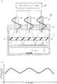
- FIG. 1Ais a schematic cross-sectional view showing an example of a plasma processing apparatus 20 according to a comparative example
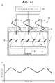
- FIG. 1Bis a schematic cross-sectional view showing an example of the plasma processing apparatus 10 according to an embodiment.
- a microwave plasma processing apparatuswill be described as an example of the plasma processing apparatuses 10 and 20 .
- the plasma processing apparatus 20 according to the comparative example shown in part (a) of FIG. 1Adoes not include a phase shifter.
- the plasma processing apparatus 10includes a chamber 1 accommodating a wafer W.
- the plasma processing apparatus 10performs predetermined plasma processing such as film formation, etching, or the like on the wafer W using surface wave plasma generated by microwaves.
- the chamber 1is a substantially cylindrical processing container and is grounded.
- the inside of the chamber 1can be maintained in an airtight state by closing an upper opening formed at a ceiling portion of the chamber 1 with a ceiling plate 9 .
- the chamber 1 and the ceiling plate 9are made of a metal material such as aluminum, stainless steel, or the like.
- a stage 3 on which the wafer W is placedis supported at a bottom center of the chamber 1 by a cylindrical support member 4 extending upward through an insulating member.
- the stage 3may be made of, e.g., a metal such as aluminum having an alumite-treated (anodically oxidized) surface, or may be made of an insulating member (ceramic or the like) having therein a radio frequency electrode.
- the stage 3may be provided with an electrostatic chuck for attracting and holding the wafer W, a temperature control mechanism, a gas flow path for supplying a heat transfer gas to the backside of the wafer W, and the like.
- a radio frequency bias power supplymay be electrically connected to the stage 3 through a matcher. By supplying a radio frequency power from the radio frequency bias power supply to the stage 3 , ions in the plasma are attracted toward the wafer W.
- the radio frequency bias power supplymay not be provided depending on characteristics of plasma processing.
- An exhaust lineis connected to the bottom portion of the chamber 1 .
- An exhaust including a vacuum pumpis connected to the exhaust line. When the exhaust is driven, a gas in the chamber 1 is exhausted and a pressure in the chamber is reduced to a predetermined degree of vacuum.
- a loading/unloading port for loading and unloading the wafer W and a gate valve for opening and closing the loading/unloading portare disposed on a sidewall of the chamber 1 .
- the ceiling plate 9is provided with seven electromagnetic wave radiating devices 2 for radiating microwaves into the chamber 1 (only three electromagnetic wave radiating devices 2 are shown in part (a) of FIG. 1B ).
- FIG. 2shows an example of the electromagnetic wave radiating device 2 .
- the electromagnetic wave radiating device 2has a coaxial cable shape, and includes an inner conductor 121 , an outer conductor 122 disposed on an outer side of the inner conductor 121 , and a dielectric 123 such as Teflon (Registered Trademark) or the like disposed between the inner conductor 121 and the outer conductor 122 .
- a tip end of the electromagnetic wave radiating device 2constitutes a monopole antenna 11 formed of the inner conductor 121 projecting by a length D.
- the monopole antenna 11constitutes a radiating device 125 by exposing the inner conductor 121 from the end surface of the dielectric 123 at the same height as that of a back surface 9 a of the ceiling plate 9 of the chamber 1 into the inner space of the chamber 1 , so that the microwaves are radiated from the radiating device 125 into the chamber 1 .
- the length D of the radiating device 125varies depending on the frequency of the electromagnetic wave. For example, when the frequency of the microwave is 300 MHz to 3 GHz, the length D is several tens of mm to several hundreds of mm. However, the inner conductor 121 may not project from the dielectric 123 .
- a notch portion in which the outer conductor 122 is not disposedis formed at the tip end of the electromagnetic wave radiating device 2 , and the microwaves are radiated into the chamber 1 from a radiation port at the tip end of the inner conductor 121 through the notch portion.
- the electromagnetic wave radiating devices 2are arranged at approximately equal intervals such that a distance E between centers of two adjacent electromagnetic wave radiating devices 2 becomes smaller than 1 ⁇ 2 of a wavelength A of the microwave.
- a dielectric window 5is disposed so as to be separated from a plurality of radiating devices 125 and the stage 3 .
- the dielectric window 5is a partition plate that divides the inside of the chamber 1 into a space V above the dielectric window 5 and a space U below the dielectric window 5 .
- the dielectric window 5is made of, e.g., ceramics such as quartz and alumina (Al 2 O 3 ), a fluorine-based resin such as polytetrafluoroethylene or the like, or a polyimide-based resin.
- a free space of about several tens of mm to several hundreds of mmexists in the space V below the electromagnetic wave radiating device 2 , and plasma is generated in the space U through the dielectric window 5 disposed below the free space.
- a vertical distance H between the back surface 9 a of the ceiling plate 9 and the upper surface of the dielectric window 5is greater than ⁇ /4 with respect to the wavelength A of the microwave.
- a plurality of microwaves radiated from the seven electromagnetic wave radiating devices 2propagate in the space V.
- the space Vis an atmospheric space
- the space Uis a vacuum space.
- the plasma processing apparatus 10includes the controller 8 .
- the controller 8may be a computer including a processor, a storage such as a memory or the like, an input device, a display device, a signal input/output interface, and the like.
- the controller 8controls individual components of the plasma processing apparatus 10 .
- an operatorcan input a command to manage the plasma processing apparatus 10 using the input device.
- an operation status of the plasma processing apparatus 10can be visualized and displayed by the display device.
- a control program and recipe dataare stored in the storage.
- the control programis executed by the processor to execute various processes in the plasma processing apparatus 10 .
- the processorexecutes the control program and controls the individual components of the plasma processing apparatus 10 based on the recipe data.
- the processor of the controller 8controls the phase shifter 7 provided for each electromagnetic wave radiating device 2 and controls the phases of the microwaves radiated from the radiating device 125 .
- the wafer W held on a transfer armis loaded into the chamber 1 from an open gate valve through the loading/unloading port.
- the gate valveis closed after the wafer W is loaded.
- the wafer Wis delivered from the transfer arm to a pusher pin, and is placed on the stage 3 by lowering the pusher pin.
- the pressure in the chamber 1is maintained at a predetermined degree of vacuum by the exhaust.
- a predetermined gasis introduced into the space U below the dielectric window 5 .
- the phase-controlled microwavesare radiated from the seven electromagnetic wave radiating devices 2 (the monopole antennas 11 ). Accordingly, the electric field becomes strong at a predetermined position of the dielectric window 5 , and the distribution of the plasma of the gas can be controlled.
- Predetermined plasma processingis performed on the wafer W by the generated plasma.
- the phases of the microwaves radiated from the seven electromagnetic wave radiating devices 2are the same, as indicated by thick curved lines in the electromagnetic wave radiating devices 2 . Therefore, in the plasma processing apparatus 20 according to the comparative example, when the plasma is generated below the dielectric window 5 by the microwave electric field, the electric field distribution is affected by the arrangement pattern of the seven electromagnetic wave radiating devices 2 . As a result, as shown in part (b) of FIG. 1A , the plasma distribution varies depending on the arrangement pattern of the electromagnetic wave radiating devices 2 . In other words, the plasma processing on the wafer W tends to be non-uniform due to the influence of the arrangement pattern of the electromagnetic wave radiating devices 2 .
- the plasma processing apparatus 10 and the plasma processing method of the present embodimentcan control the plasma distribution by changing the electric field distribution in the dielectric window 5 regardless of the arrangement of the electromagnetic wave radiating devices 2 .
- the phases of the microwaves radiated from the seven electromagnetic wave radiating devices 2are controlled using the phase shifters 7 under the control of the controller 8 . Accordingly, the microwaves inputted from the seven electromagnetic wave radiating devices 2 interfere, and the electric field can be strengthened at a certain position. Hence, the plasma distribution can be controlled with high accuracy by concentrating the plasma.
- the microwaves propagating in the space Vinterfere due to the phase control of the microwaves inputted from the seven electromagnetic wave radiating devices 2 , so that the strength of the microwave electric field becomes strong on a left side of the dielectric window 5 .
- FIGS. 3A to 3Cexplain the phase control using the phase shifter 7 performed by the controller 8 of the plasma processing apparatus 10 according to one embodiment.
- FIG. 3Ashows the relationship between the microwaves radiated from one of the electromagnetic wave radiating devices 2 (an electromagnetic wave radiating device 2 a in this example) and a focal position O at which the electric field should be concentrated in the dielectric window 5 .
- (1)is satisfied when the position on the back surface of the ceiling plate 9 perpendicular to the focal position O is set to O′; the distance from the focal position O to the position O′ on the back surface of the ceiling plate 9 is set to z; and the radiation position of the microwaves radiated from the electromagnetic wave radiating device 2 a is set to x.
- ⁇ (x)indicates the phase of the electromagnetic wave (microwave in the present embodiment) radiated from the radiation position x.
- Eq. (2) for obtaining the phase ⁇ (x) of the electromagnetic waveis obtained by transforming Eq. (1).
- the phase ⁇ (x) of the electromagnetic wave radiated from the radiation position xis calculated from the wave number k of the electromagnetic wave, the distance z from the position O on the dielectric window 5 to the position O′ on the back surface of the ceiling plate 9 , and the radiation position x.
- Eq. (2)is expressed by the curve of FIG. 3B .
- the conditions for strengthening the phases of the microwaves radiated from two or more electromagnetic wave radiating devices 2 at the focal position Owill be described with reference to FIG. 3C .
- the seven electromagnetic wave radiating devices 2include electromagnetic wave radiating devices 2 a , 2 b , 2 c , 2 d , 2 e , 2 f , and 2 g .
- FIG. 3Cfor convenience of description, they are arranged horizontally while being spaced apart from each other unlike the actual positional relationship of the electromagnetic wave radiating devices 2 .
- the controller 8controls phases ⁇ (x a ) to ⁇ (x g ) of the microwaves radiated from the electromagnetic wave radiating devices 2 a to 2 g to be matched at the focal position O in the respective distances from radiation positions x a to x g of the microwaves radiated from the electromagnetic wave radiating devices 2 a to 2 g to the focal position O.
- the phases ⁇ (x) of the microwaves radiated from the electromagnetic wave radiating devices 2 a to 2 gare different from each other at the focal position O if the phase control is not performed. Accordingly, even if any of the microwaves radiated from the electromagnetic wave radiating devices 2 a to 2 g is in a condition of strengthening the phases at the focal position O, any of the other microwaves is in a condition of weakening the phases at the focal position O.
- the phases of all the microwavescan be strengthened at the focal position O by controlling the phases ⁇ (x a ) to ⁇ (x g ) of the microwaves radiated from the electromagnetic wave radiating devices 2 a to 2 g , respectively.
- the phases of the microwaves radiated from the electromagnetic wave radiating devices 2 a , 2 b , and 2 c shown in FIG. 3Care in a condition of strengthening the phase of the microwave because antinodes coincide with each other, and nodes coincide with each other.
- the phase of at least one microwave radiated from the electromagnetic wave radiating devices 2 d to 2 gmay be weakened. In other words, all the phases of the seven microwaves may not be strengthened at the focal position O.
- the phases of the microwaves radiated from the electromagnetic wave radiating devices 2 d , 2 e , 2 f , and 2 gare also controlled under a condition of strengthening the microwaves. Accordingly, the phase of each microwave is controlled under a condition that the phases of the seven microwaves are strengthened at the focal position O on the dielectric window 5 , which makes it possible to control the microwave electric field to be concentrated at the focal position O.
- the control for strengthening the phases of the microwaves at the focal position Ois performed on two microwaves having the lowest phase outputted from the electromagnetic wave radiating devices 2 a to 2 g , and may not be performed on all the seven microwaves.
- the phases of the microwaves of one or more electromagnetic wave radiating devices 2may not be controlled.
- one focal position Oexists on the dielectric window 5 .
- the present disclosureis not limited thereto, and it is also possible to perform the control for strengthening the phases at two or more focal positions O on the dielectric window 5 at the same timing.
- the distance E from the center of one electromagnetic wave radiating device 2 to the center of an adjacent electromagnetic wave radiating device 2is smaller than ⁇ /2. If the distance E (interval) between the adjacent electromagnetic wave radiating devices 2 is greater than ⁇ /2, the microwaves cannot be concentrated at the focal position O on the dielectric window 5 , and it is not possible to perform the control of strengthening the phases of the microwaves at the focal position O.
- the concentration of microwaves by the phase control described abovedoes not require a mechanical operation, and thus can be controlled at a high speed.
- the phase control of the electromagnetic wave radiating devices 2can be performed at a high speed.
- plasmacan be uniformly formed in the space U below the dielectric window 5 by controlling the distribution of the microwave electric field in the dielectric window 5 at a high speed.
- FIG. 4shows an example of the phase control performed by the controller 8 according to an embodiment.
- the controller 8uses the phase shifters (only one is shown in FIG. 4 ) to control the phases ⁇ (x a ) to ⁇ (x g ) of the microwaves radiated from the seven electromagnetic wave radiating devices 2 a to 2 g to be strengthened at the focal position C.
- the microwave electric fieldis controlled to be strengthened at a focusing portion Ar centered on the focal position C.
- the controller 8uses the phase shifters 7 to control the microwave phases ⁇ (x a ) to ⁇ (x g ) at a high speed such that the focal position C scans the surface of the dielectric window 5 in a radial direction L 1 or in a circumferential direction L 2 . Accordingly, plasma can be uniformly formed in the space U below the dielectric window 5 by moving the focal position C and the focusing portion Ar at a high speed.
- the controller 8changes the moving speed of the focusing portion Ar by changing the speed of controlling the phases ⁇ (x a ) to ⁇ (x g ) of the microwaves using the phase shifters 7 . Accordingly, average electric field distribution per unit time can be freely controlled.
- the controller 8may change the speed of controlling the phases ⁇ (x a ) to ⁇ (x g ) of the microwaves such that the focusing portion Ar moves slowly on an outer peripheral side of the dielectric window 5 and moves faster on an inner peripheral side of the dielectric window 5 .
- the electric field strength on the outer peripheral side of the dielectric window 5can become stronger than that on the inner peripheral side of the dielectric window 5 .
- the plasma distributioncan be freely controlled such as controlling the plasma density on the outer peripheral side below the dielectric window 5 to be higher than the plasma density on the inner peripheral side.
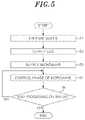
- FIG. 5is a flowchart showing an example of the plasma processing method according to an embodiment. This processing is controlled by the controller 8 .
- the controller 8prepares the wafer W by loading the wafer W into the chamber and placing it on the stage 3 (step S 1 ). Next, the controller 8 supplies a predetermined gas from a gas supply (step S 2 ). Next, the controller 8 outputs microwaves from the microwave output unit 6 (step S 3 ).
- the electromagnetic wave radiating devices 2 of the plasma processing apparatus 10 of the present disclosuremay radiate electromagnetic waves having a frequency of 100 MHz or higher, such as UHF or the like, other than microwaves. More preferably, the electromagnetic wave radiating devices 2 may radiate electromagnetic waves having a frequency within a range of 1 GHz to 3 GHz.
- the phase controlcan be performed at a higher speed as the frequency becomes higher.
- the space V above the dielectric window 5is set to an atmospheric space.
- the present disclosureis not limited thereto.
- the space V above the dielectric window 5may be filled with a dielectric made of material that is the same as or different from that of the dielectric window 5 .
- the wavelength of the microwaves propagating in the dielectriccan be shortened by filling the space V with the dielectric, which makes it possible to make the plasma processing apparatus 10 small.
- the space V above the dielectric window 5is set to an atmospheric space.
- the space Vmay be set to a vacuum space.
- the phase controlis performed in the vacuum space and, thus, plasma may be formed in the space V. Therefore, it is more preferable to set the space V above the dielectric window 5 to an atmospheric space.
Landscapes
- Physics & Mathematics (AREA)
- Engineering & Computer Science (AREA)
- Plasma & Fusion (AREA)
- Chemical & Material Sciences (AREA)
- Analytical Chemistry (AREA)
- Electromagnetism (AREA)
- Spectroscopy & Molecular Physics (AREA)
- Condensed Matter Physics & Semiconductors (AREA)
- General Physics & Mathematics (AREA)
- Manufacturing & Machinery (AREA)
- Computer Hardware Design (AREA)
- Microelectronics & Electronic Packaging (AREA)
- Power Engineering (AREA)
- Plasma Technology (AREA)
- Drying Of Semiconductors (AREA)
Abstract
Description
- The present disclosure relates to a plasma processing method and a plasma processing apparatus.
- There is known a plasma processing apparatus for forming plasma of a gas by a power of electromagnetic waves and performing plasma processing on a wafer. For example,
Patent Document 1 discloses a plasma processing apparatus including a processing chamber for forming plasma, a vacuum window forming a part of a wall of the processing chamber, induction antennas disposed outside a dielectric of the vacuum window and including at least two systems for forming plasma in the processing chamber, radio frequency power supplies for making currents flow in the induction antennas independently, and a control unit including phase circuits, a controller, or the like for controlling phases of the currents or current values of the radio frequency power supplies of the respective systems over time. The control unit ofPatent Document 1 continuously performs time modulation of a phase difference between the currents flowing in the systems or the current values within a sample processing period and moves a plasma generation position to make an incident angle of ions on a wafer uniform in a wafer plane. - For example,
Patent Document 2 suggests a method for modifying a reaction rate on a semiconductor substrate in a processing chamber using a phased-array microwave antenna. This method includes: exciting plasma in the processing chamber; emitting microwave radiation beam from the phased-array microwave antenna; and directing the beam to the plasma to change the reaction rate on a surface of the semiconductor substrate in the processing chamber. - For example,
Patent Document 3 suggests an apparatus for radiating microwaves outputted from a microwave output unit into a chamber from an antenna and generating an electric field for generating surface wave plasma in a dielectric member that transmits the microwaves radiated from the antenna. InPatent Document 3, at least one of the power and the phase of the microwaves radiated to a microwave radiation mechanism is controlled based on an electron temperature Te of the plasma and an electron density Ne of the plasma. - Patent Document 1: Japanese Patent Application Publication No. 2015-53172
- Patent Document 2: Japanese Patent Application Publication No. 2017-103454
- Patent Document 3: Japanese Patent Application Publication No. 2018-181634
- The present disclosure provides a plasma processing method and a plasma processing apparatus capable of changing electric field distribution in a dielectric window regardless of arrangement of a plurality of electromagnetic wave radiating devices.
- In accordance with one aspect of the present disclosure, there is provided a plasma processing method in a plasma processing apparatus including a chamber, a stage on which a substrate is placed in the chamber, a plurality of radiating devices configured to radiate a plurality of electromagnetic waves, and a dielectric window disposed between the plurality of radiating devices and the stage. The method comprises preparing the substrate on the stage, controlling a phase of at least one of the plurality of electromagnetic waves radiated from the plurality of radiating devices, radiating the plurality of electromagnetic waves into the chamber from the plurality of radiating devices, and processing the substrate using localized plasma generated from a gas supplied between the dielectric window and the stage.
- In accordance with one aspect, it is possible to change the electric field distribution in the dielectric window regardless of the arrangement of the electromagnetic wave radiating devices.
FIG. 1A is a schematic cross-sectional view showing an example of a plasma processing apparatus according to a comparative example.FIG. 1B is a schematic cross-sectional view showing an example of a plasma processing apparatus according to an embodiment.FIG. 2 shows an example of an electromagnetic wave radiating device according to an embodiment.FIG. 3 explains phase control according to an embodiment.FIG. 4 shows an example of phase control performed by a controller according to an embodiment.FIG. 5 is a flowchart showing an example of a plasma processing method according to an embodiment.FIGS. 6A to 6C show examples of electric field distribution in a dielectric window according to an embodiment.- Hereinafter, embodiments will be described in detail with reference to the accompanying drawings. Like reference numerals will be given to like parts throughout the drawings, and redundant description thereof may be omitted.
- (Plasma Processing Apparatus)
- A
plasma processing apparatus 10 according to the embodiment will be described with reference toFIGS. 1A and 1B .FIG. 1A is a schematic cross-sectional view showing an example of aplasma processing apparatus 20 according to a comparative example, andFIG. 1B is a schematic cross-sectional view showing an example of theplasma processing apparatus 10 according to an embodiment. A microwave plasma processing apparatus will be described as an example of theplasma processing apparatuses plasma processing apparatus 20 according to the comparative example shown in part (a) ofFIG. 1A does not include a phase shifter. - The
plasma processing apparatus 10 according to an embodiment shown in part (a) ofFIG. 1B includes achamber 1 accommodating a wafer W. Theplasma processing apparatus 10 performs predetermined plasma processing such as film formation, etching, or the like on the wafer W using surface wave plasma generated by microwaves. - The
chamber 1 is a substantially cylindrical processing container and is grounded. The inside of thechamber 1 can be maintained in an airtight state by closing an upper opening formed at a ceiling portion of thechamber 1 with a ceiling plate9. Thechamber 1 and the ceiling plate9 are made of a metal material such as aluminum, stainless steel, or the like. - A
stage 3 on which the wafer W is placed is supported at a bottom center of thechamber 1 by a cylindrical support member4 extending upward through an insulating member. Thestage 3 may be made of, e.g., a metal such as aluminum having an alumite-treated (anodically oxidized) surface, or may be made of an insulating member (ceramic or the like) having therein a radio frequency electrode. Thestage 3 may be provided with an electrostatic chuck for attracting and holding the wafer W, a temperature control mechanism, a gas flow path for supplying a heat transfer gas to the backside of the wafer W, and the like. - Further, a radio frequency bias power supply may be electrically connected to the
stage 3 through a matcher. By supplying a radio frequency power from the radio frequency bias power supply to thestage 3, ions in the plasma are attracted toward the wafer W. However, the radio frequency bias power supply may not be provided depending on characteristics of plasma processing. - An exhaust line is connected to the bottom portion of the
chamber 1. An exhaust including a vacuum pump is connected to the exhaust line. When the exhaust is driven, a gas in thechamber 1 is exhausted and a pressure in the chamber is reduced to a predetermined degree of vacuum. A loading/unloading port for loading and unloading the wafer W and a gate valve for opening and closing the loading/unloading port are disposed on a sidewall of thechamber 1. - The ceiling plate9 is provided with seven electromagnetic wave
radiating devices 2 for radiating microwaves into the chamber1 (only three electromagnetic waveradiating devices 2 are shown in part (a) ofFIG. 1B ). - (Monopole Antenna)
FIG. 2 shows an example of the electromagnetic waveradiating device 2. The electromagnetic waveradiating device 2 has a coaxial cable shape, and includes aninner conductor 121, anouter conductor 122 disposed on an outer side of theinner conductor 121, and a dielectric123 such as Teflon (Registered Trademark) or the like disposed between theinner conductor 121 and theouter conductor 122. A tip end of the electromagnetic waveradiating device 2 constitutes amonopole antenna 11 formed of theinner conductor 121 projecting by a length D.- The
monopole antenna 11 constitutes aradiating device 125 by exposing theinner conductor 121 from the end surface of the dielectric123 at the same height as that of aback surface 9aof the ceiling plate9 of thechamber 1 into the inner space of thechamber 1, so that the microwaves are radiated from theradiating device 125 into thechamber 1. The length D of theradiating device 125 varies depending on the frequency of the electromagnetic wave. For example, when the frequency of the microwave is 300 MHz to 3 GHz, the length D is several tens of mm to several hundreds of mm. However, theinner conductor 121 may not project from the dielectric123. In this case, a notch portion in which theouter conductor 122 is not disposed is formed at the tip end of the electromagneticwave radiating device 2, and the microwaves are radiated into thechamber 1 from a radiation port at the tip end of theinner conductor 121 through the notch portion. - With this configuration, the microwaves are outputted from a
microwave output unit 6 and radiated into thechamber 1 after the phases thereof are controlled by aphase shifter 7 under the control of acontroller 8. The number of the electromagneticwave radiating devices 2 is not limited to seven, and may be two or more, preferably three or more. - Referring back to part (a) of
FIG. 1B , the electromagneticwave radiating devices 2 are arranged at approximately equal intervals such that a distance E between centers of two adjacent electromagneticwave radiating devices 2 becomes smaller than ½ of a wavelength A of the microwave. Adielectric window 5 is disposed so as to be separated from a plurality of radiatingdevices 125 and thestage 3. Thedielectric window 5 is a partition plate that divides the inside of thechamber 1 into a space V above thedielectric window 5 and a space U below thedielectric window 5. Thedielectric window 5 is made of, e.g., ceramics such as quartz and alumina (Al2O3), a fluorine-based resin such as polytetrafluoroethylene or the like, or a polyimide-based resin. - A free space of about several tens of mm to several hundreds of mm exists in the space V below the electromagnetic
wave radiating device 2, and plasma is generated in the space U through thedielectric window 5 disposed below the free space. A vertical distance H between theback surface 9aof the ceiling plate9 and the upper surface of thedielectric window 5 is greater than λ/4 with respect to the wavelength A of the microwave. A plurality of microwaves radiated from the seven electromagneticwave radiating devices 2 propagate in the space V. The space V is an atmospheric space, and the space U is a vacuum space. - The
plasma processing apparatus 10 includes thecontroller 8. Thecontroller 8 may be a computer including a processor, a storage such as a memory or the like, an input device, a display device, a signal input/output interface, and the like. Thecontroller 8 controls individual components of theplasma processing apparatus 10. In thecontroller 8, an operator can input a command to manage theplasma processing apparatus 10 using the input device. Further, in thecontroller 8, an operation status of theplasma processing apparatus 10 can be visualized and displayed by the display device. Further, a control program and recipe data are stored in the storage. The control program is executed by the processor to execute various processes in theplasma processing apparatus 10. The processor executes the control program and controls the individual components of theplasma processing apparatus 10 based on the recipe data. Further, the processor of thecontroller 8 controls thephase shifter 7 provided for each electromagneticwave radiating device 2 and controls the phases of the microwaves radiated from the radiatingdevice 125. - In the case of performing plasma processing in the
plasma processing apparatus 10 configured as described above, first, the wafer W held on a transfer arm is loaded into thechamber 1 from an open gate valve through the loading/unloading port. - The gate valve is closed after the wafer W is loaded. When the wafer W is transferred to a position above the
stage 3, the wafer W is delivered from the transfer arm to a pusher pin, and is placed on thestage 3 by lowering the pusher pin. The pressure in thechamber 1 is maintained at a predetermined degree of vacuum by the exhaust. A predetermined gas is introduced into the space U below thedielectric window 5. The phase-controlled microwaves are radiated from the seven electromagnetic wave radiating devices2 (the monopole antennas11). Accordingly, the electric field becomes strong at a predetermined position of thedielectric window 5, and the distribution of the plasma of the gas can be controlled. Predetermined plasma processing is performed on the wafer W by the generated plasma. - In the
plasma processing apparatus 20 according to the comparative example shown in part (a) ofFIG. 1A , the phases of the microwaves radiated from the seven electromagneticwave radiating devices 2 are the same, as indicated by thick curved lines in the electromagneticwave radiating devices 2. Therefore, in theplasma processing apparatus 20 according to the comparative example, when the plasma is generated below thedielectric window 5 by the microwave electric field, the electric field distribution is affected by the arrangement pattern of the seven electromagneticwave radiating devices 2. As a result, as shown in part (b) ofFIG. 1A , the plasma distribution varies depending on the arrangement pattern of the electromagneticwave radiating devices 2. In other words, the plasma processing on the wafer W tends to be non-uniform due to the influence of the arrangement pattern of the electromagneticwave radiating devices 2. - However, it is difficult to change the arrangement pattern of the electromagnetic
wave radiating devices 2, which is the physical arrangement, from the preset arrangement. Therefore, theplasma processing apparatus 10 and the plasma processing method of the present embodiment can control the plasma distribution by changing the electric field distribution in thedielectric window 5 regardless of the arrangement of the electromagneticwave radiating devices 2. - In other words, in the
plasma processing apparatus 10 according to the present embodiment shown in part (a) ofFIG. 1B , the phases of the microwaves radiated from the seven electromagneticwave radiating devices 2 are controlled using thephase shifters 7 under the control of thecontroller 8. Accordingly, the microwaves inputted from the seven electromagneticwave radiating devices 2 interfere, and the electric field can be strengthened at a certain position. Hence, the plasma distribution can be controlled with high accuracy by concentrating the plasma. - For example, in part (a) of
FIG. 1B , the microwaves propagating in the space V interfere due to the phase control of the microwaves inputted from the seven electromagneticwave radiating devices 2, so that the strength of the microwave electric field becomes strong on a left side of thedielectric window 5. Thus, it is possible to concentrate plasma on a left side of the wafer W, as shown in part (b) ofFIG. 1B . - (Phase Control)
- Next, the microwave phase control will be described with reference to
FIGS. 3A to 3C .FIGS. 3A to 3C explain the phase control using thephase shifter 7 performed by thecontroller 8 of theplasma processing apparatus 10 according to one embodiment.FIG. 3A shows the relationship between the microwaves radiated from one of the electromagnetic wave radiating devices2 (an electromagneticwave radiating device 2ain this example) and a focal position O at which the electric field should be concentrated in thedielectric window 5. The following Eq. (1) is satisfied when the position on the back surface of the ceiling plate9 perpendicular to the focal position O is set to O′; the distance from the focal position O to the position O′ on the back surface of the ceiling plate9 is set to z; and the radiation position of the microwaves radiated from the electromagneticwave radiating device 2ais set to x.
[Eq. 1]
k√{square root over (x2+z2)}−δ(x)=kz (1)- K in Eq. (1) indicates a wave number of an electromagnetic wave and is represented by a reciprocal of the wavelength λ of the electromagnetic wave, i.e., k=1/λ. δ(x) indicates the phase of the electromagnetic wave (microwave in the present embodiment) radiated from the radiation position x.
- Eq. (2) for obtaining the phase δ(x) of the electromagnetic wave is obtained by transforming Eq. (1).
[Eq. 2]
δ(x)=k(√{square root over (x2+z2)}−z) (2)- Based on Eq. (2), the phase δ(x) of the electromagnetic wave radiated from the radiation position x is calculated from the wave number k of the electromagnetic wave, the distance z from the position O on the
dielectric window 5 to the position O′ on the back surface of the ceiling plate9, and the radiation position x. Eq. (2) is expressed by the curve ofFIG. 3B . - The conditions for strengthening the phases of the microwaves radiated from two or more electromagnetic
wave radiating devices 2 at the focal position O will be described with reference toFIG. 3C . The seven electromagneticwave radiating devices 2 include electromagneticwave radiating devices FIG. 3C , for convenience of description, they are arranged horizontally while being spaced apart from each other unlike the actual positional relationship of the electromagneticwave radiating devices 2. - In the case of controlling the electromagnetic
wave radiating devices 2ato2gaccording to the present embodiment, thecontroller 8 controls phases δ(xa) to δ(xg) of the microwaves radiated from the electromagneticwave radiating devices 2ato2gto be matched at the focal position O in the respective distances from radiation positions xato xgof the microwaves radiated from the electromagneticwave radiating devices 2ato2gto the focal position O. - Since the radiation positions x of the electromagnetic
wave radiating devices 2ato2gare different, as shown in Eq. (2), the phases δ(x) of the microwaves radiated from the electromagneticwave radiating devices 2ato2gare different from each other at the focal position O if the phase control is not performed. Accordingly, even if any of the microwaves radiated from the electromagneticwave radiating devices 2ato2gis in a condition of strengthening the phases at the focal position O, any of the other microwaves is in a condition of weakening the phases at the focal position O. On the other hand, in the present embodiment, the phases of all the microwaves can be strengthened at the focal position O by controlling the phases δ(xa) to δ(xg) of the microwaves radiated from the electromagneticwave radiating devices 2ato2g, respectively. For example, the phases of the microwaves radiated from the electromagneticwave radiating devices FIG. 3C are in a condition of strengthening the phase of the microwave because antinodes coincide with each other, and nodes coincide with each other. However, even if it is controlled to strengthen the phases of the microwaves radiated from the electromagneticwave radiating devices wave radiating devices 2dto2gmay be weakened. In other words, all the phases of the seven microwaves may not be strengthened at the focal position O. - On the other hand, in the present embodiment, the phases of the microwaves radiated from the electromagnetic
wave radiating devices dielectric window 5, which makes it possible to control the microwave electric field to be concentrated at the focal position O. - However, the control for strengthening the phases of the microwaves at the focal position O is performed on two microwaves having the lowest phase outputted from the electromagnetic
wave radiating devices 2ato2g, and may not be performed on all the seven microwaves. For example, the phases of the microwaves of one or more electromagneticwave radiating devices 2 may not be controlled. In the above description, one focal position O exists on thedielectric window 5. However, the present disclosure is not limited thereto, and it is also possible to perform the control for strengthening the phases at two or more focal positions O on thedielectric window 5 at the same timing. - As shown in part (a) of
FIG. 1B , the distance E from the center of one electromagneticwave radiating device 2 to the center of an adjacent electromagneticwave radiating device 2 is smaller than λ/2. If the distance E (interval) between the adjacent electromagneticwave radiating devices 2 is greater than λ/2, the microwaves cannot be concentrated at the focal position O on thedielectric window 5, and it is not possible to perform the control of strengthening the phases of the microwaves at the focal position O. - The concentration of microwaves by the phase control described above does not require a mechanical operation, and thus can be controlled at a high speed. In principle, it is possible to move the focal position O over time with high-speed control comparable to the microwave frequency. Accordingly, the phase control of the electromagnetic
wave radiating devices 2 can be performed at a high speed. As a result, plasma can be uniformly formed in the space U below thedielectric window 5 by controlling the distribution of the microwave electric field in thedielectric window 5 at a high speed. FIG. 4 shows an example of the phase control performed by thecontroller 8 according to an embodiment. In the example ofFIG. 4 , thecontroller 8 uses the phase shifters (only one is shown inFIG. 4 ) to control the phases δ(xa) to δ(xg) of the microwaves radiated from the seven electromagneticwave radiating devices 2ato2gto be strengthened at the focal position C. Thereby, it is schematically shown that the microwave electric field is controlled to be strengthened at a focusing portion Ar centered on the focal position C.- The
controller 8 uses thephase shifters 7 to control the microwave phases δ(xa) to δ(xg) at a high speed such that the focal position C scans the surface of thedielectric window 5 in a radial direction L1 or in a circumferential direction L2. Accordingly, plasma can be uniformly formed in the space U below thedielectric window 5 by moving the focal position C and the focusing portion Ar at a high speed. - Further, the
controller 8 changes the moving speed of the focusing portion Ar by changing the speed of controlling the phases δ(xa) to δ(xg) of the microwaves using thephase shifters 7. Accordingly, average electric field distribution per unit time can be freely controlled. For example, thecontroller 8 may change the speed of controlling the phases δ(xa) to δ(xg) of the microwaves such that the focusing portion Ar moves slowly on an outer peripheral side of thedielectric window 5 and moves faster on an inner peripheral side of thedielectric window 5. Hence, the electric field strength on the outer peripheral side of thedielectric window 5 can become stronger than that on the inner peripheral side of thedielectric window 5. As a result, the plasma distribution can be freely controlled such as controlling the plasma density on the outer peripheral side below thedielectric window 5 to be higher than the plasma density on the inner peripheral side. - (Plasma Processing Method)
- Next, an example of the plasma processing method performed by the
plasma processing apparatus 10 will be described with reference toFIG. 5 .FIG. 5 is a flowchart showing an example of the plasma processing method according to an embodiment. This processing is controlled by thecontroller 8. - When this processing is started, the
controller 8 prepares the wafer W by loading the wafer W into the chamber and placing it on the stage3 (step S1). Next, thecontroller 8 supplies a predetermined gas from a gas supply (step S2). Next, thecontroller 8 outputs microwaves from the microwave output unit6 (step S3). - Next, the
controller 8 uses thephase shifters 7 to control the phases of the microwaves radiated from the seven electromagneticwave radiating devices 2, and radiates the phase-controlled microwaves from the radiatingdevices 125 of the electromagneticwave radiating devices 2 into the chamber (step S4). Accordingly, the phase-controlled microwaves interfere with each other in the space V, and the microwaves can be concentrated at a predetermined position on thedielectric window 5. Hence, localized plasma is formed in the space U between thedielectric window 5 and thestage 3, and predetermined plasma processing is performed on the wafer W using the formed localized plasma. - Next, the
controller 8 determines whether to end the plasma processing on the wafer W (step S5). Thecontroller 8 controls the phases of the microwaves outputted from the seven electromagneticwave radiating devices 2 over time until it is determined to end the plasma processing on the wafer W based on the recipe (step S4). Thecontroller 8 ends this processing when it is determined to end the plasma processing on the wafer W based on the recipe. When this processing is ended, the microwave output is stopped, and the gas supply is stopped. - (Phase Control Simulation Result)
FIGS. 6B and 6C show examples of the simulation result of the electric field distribution in thedielectric window 5 according to an embodiment in the case where thecontroller 8 controls the phases of the microwaves outputted from nineteen electromagneticwave radiating devices 2 using thephase shifters 7 as shown inFIG. 6A .- This simulation was performed under the condition of radiating microwaves of the same power from the nineteen electromagnetic
wave radiating devices 2. InFIGS. 6A, 6B and6C, darker portions indicate higher electric field strength of microwaves. - In the case of controlling the phases δ(x) of the microwaves to be strengthened at a focal position C1 of the
dielectric window 5, the microwave electric field became strong at the focusing portion Ar centered on the focal position C1 as shown inFIG. 6B . - Then, the phases of the microwaves radiated from the nineteen electromagnetic
wave radiating devices 2 were controlled using thephase shifters 7 such that the focusing portion Ar where the microwave electric field is strong moves toward the center in the radial direction.FIG. 6C shows an example of the simulation result of the electric field distribution in thedielectric window 5 at this time. According to this, it was possible to move the portion where the microwave electric field is strong to the focusing portion Ar centered on a focal position C2. This simulation has confirmed that free focusing control can be performed by the phase control. - As described above, in accordance with the
plasma processing apparatus 10 of the present embodiment, the electric field distribution in thedielectric window 5 can be changed regardless of the arrangement of the electromagneticwave radiating devices 2. Accordingly, free focusing control can be performed by the phase control, and the plasma distribution can be freely controlled. - Although a plasma processing apparatus that radiates microwaves has been described as an example of the
plasma processing apparatus 10 of the present disclosure, the present disclosure is not limited thereto. The electromagneticwave radiating devices 2 of theplasma processing apparatus 10 of the present disclosure may radiate electromagnetic waves having a frequency of 100 MHz or higher, such as UHF or the like, other than microwaves. More preferably, the electromagneticwave radiating devices 2 may radiate electromagnetic waves having a frequency within a range of 1 GHz to 3 GHz. The phase control can be performed at a higher speed as the frequency becomes higher. - In the above-described embodiment, the space V above the
dielectric window 5 is set to an atmospheric space. However, the present disclosure is not limited thereto. For example, the space V above thedielectric window 5 may be filled with a dielectric made of material that is the same as or different from that of thedielectric window 5. The wavelength of the microwaves propagating in the dielectric can be shortened by filling the space V with the dielectric, which makes it possible to make theplasma processing apparatus 10 small. - In the above-described embodiment, the space V above the
dielectric window 5 is set to an atmospheric space. However, the space V may be set to a vacuum space. However, when the space V is set to a vacuum space, the phase control is performed in the vacuum space and, thus, plasma may be formed in the space V. Therefore, it is more preferable to set the space V above thedielectric window 5 to an atmospheric space. By setting the distance D between the radiatingdevice 125 and thedielectric window 5 to be greater than ¼ of the wavelength λ of the microwave, the microwaves can be sufficiently focused on thedielectric window 5. - While embodiments of the plasma processing method and the plasma processing apparatus of the present disclosure have been described, the present disclosure is not limited to the above-described embodiments. Various changes, modifications, substitutions, additions, omissions, and combinations can be made without departing from the scope of the claims, and it is to be understood that these are also included in the technical scope of the present disclosure.
- This application claims priority to Japanese Patent Application No. 2019-071541, filed on Apr. 3, 2019, the entire contents of which are incorporated herein by reference.
- 1: chamber
- 2: electromagnetic wave radiating device
- 3: stage
- 5: dielectric window
- 6: microwave output unit
- 7: phase shifter
- 8: controller
- 9: ceiling plate
- 10: plasma processing apparatus
- 11: monopole antenna
- 121: inner conductor
- 122: outer conductor
- 124: notch
- 125: radiating device
Claims (9)
Applications Claiming Priority (3)
| Application Number | Priority Date | Filing Date | Title |
|---|---|---|---|
| JP2019-071541 | 2019-04-03 | ||
| JP2019071541AJP7221115B2 (en) | 2019-04-03 | 2019-04-03 | Plasma processing method and plasma processing apparatus |
| PCT/JP2020/012686WO2020203406A1 (en) | 2019-04-03 | 2020-03-23 | Plasma processing method and plasma processing device |
Publications (2)
| Publication Number | Publication Date |
|---|---|
| US20220199369A1true US20220199369A1 (en) | 2022-06-23 |
| US12243718B2 US12243718B2 (en) | 2025-03-04 |
Family
ID=72667709
Family Applications (1)
| Application Number | Title | Priority Date | Filing Date |
|---|---|---|---|
| US17/599,912Active2041-02-24US12243718B2 (en) | 2019-04-03 | 2020-03-23 | Plasma processing method and plasma processing apparatus |
Country Status (5)
| Country | Link |
|---|---|
| US (1) | US12243718B2 (en) |
| JP (1) | JP7221115B2 (en) |
| KR (1) | KR102614242B1 (en) |
| CN (1) | CN113615322B (en) |
| WO (1) | WO2020203406A1 (en) |
Cited By (1)
| Publication number | Priority date | Publication date | Assignee | Title |
|---|---|---|---|---|
| US12243718B2 (en)* | 2019-04-03 | 2025-03-04 | Tokyo Electron Limited | Plasma processing method and plasma processing apparatus |
Families Citing this family (3)
| Publication number | Priority date | Publication date | Assignee | Title |
|---|---|---|---|---|
| JP7531349B2 (en)* | 2020-08-28 | 2024-08-09 | 東京エレクトロン株式会社 | Plasma processing apparatus and plasma processing method |
| US11574808B2 (en) | 2021-02-16 | 2023-02-07 | Tokyo Electron Limited | Plasma processing method and plasma processing apparatus |
| CN113851368B (en)* | 2021-09-22 | 2023-01-31 | 大连理工大学 | Method for enhancing discharge in radio frequency magnetization capacitive coupling discharge device |
Citations (40)
| Publication number | Priority date | Publication date | Assignee | Title |
|---|---|---|---|---|
| US5234526A (en)* | 1991-05-24 | 1993-08-10 | Lam Research Corporation | Window for microwave plasma processing device |
| US5803975A (en)* | 1996-03-01 | 1998-09-08 | Canon Kabushiki Kaisha | Microwave plasma processing apparatus and method therefor |
| US6140773A (en)* | 1996-09-10 | 2000-10-31 | The Regents Of The University Of California | Automated control of linear constricted plasma source array |
| US6313584B1 (en)* | 1998-09-17 | 2001-11-06 | Tokyo Electron Limited | Electrical impedance matching system and method |
| US6527908B2 (en)* | 2000-03-21 | 2003-03-04 | Sharp Kabushiki Kaisha | Plasma process apparatus |
| US20030052085A1 (en)* | 2000-03-28 | 2003-03-20 | Richard Parsons | Control of power delivered to a multiple segment inject electrode |
| US6780278B2 (en)* | 2000-06-28 | 2004-08-24 | Kabushiki Kaisha Toshiba | Plasma processing apparatus with reduced parasitic capacity and loss in RF power |
| US20080050292A1 (en)* | 2006-08-28 | 2008-02-28 | Valery Godyak | Plasma reactor with inductie excitation of plasma and efficient removal of heat from the excitation coil |
| US20100175833A1 (en)* | 2009-01-15 | 2010-07-15 | Hitachi High-Technologies Corporation. | Plasma processing apparatus and plasma generating apparatus |
| US20100175832A1 (en)* | 2009-01-15 | 2010-07-15 | Hitachi High-Technologies Corporation | Plasma processing apparatus and plasma generating apparatus |
| US20100230053A1 (en)* | 2009-01-15 | 2010-09-16 | Ryoji Nishio | Plasma processing apparatus |
| US20110061814A1 (en)* | 2008-03-14 | 2011-03-17 | Tokyo Electron Limited | Microwave introducing mechanism, microwave plasma source and microwave plasma processing apparatus |
| WO2011040328A1 (en)* | 2009-09-29 | 2011-04-07 | 東京エレクトロン株式会社 | Antenna for generating surface wave plasma, microwave introducing mechanism, and apparatus for processing surface wave plasma |
| US20110284167A1 (en)* | 2009-01-15 | 2011-11-24 | Ryoji Nishio | Plasma processing equipment and plasma generation equipment |
| WO2013102964A1 (en)* | 2012-01-05 | 2013-07-11 | パナソニック株式会社 | Quadrature hybrid coupler, amplifier, and wireless communication device |
| US8525412B2 (en)* | 2008-11-24 | 2013-09-03 | Topanga Technologies, Inc. | Method and system for selectively tuning the frequency of a resonator assembly for a plasma lamp |
| US8773018B2 (en)* | 2011-01-25 | 2014-07-08 | Paul F. Hensley | Tuning a dielectric barrier discharge cleaning system |
| US20150015139A1 (en)* | 2013-07-10 | 2015-01-15 | Tokyo Electron Limited | Microwave plasma processing apparatus and microwave supplying method |
| US20150013907A1 (en)* | 2013-07-10 | 2015-01-15 | Tokyo Electron Limited | Microwave plasma processing apparatus, slot antenna, and semiconductor device |
| US20150013911A1 (en)* | 2013-07-10 | 2015-01-15 | Tokyo Electron Limited | Microwave plasma processing apparatus, slot antenna, and semiconductor device |
| US8988012B2 (en)* | 2010-03-31 | 2015-03-24 | Tokyo Electron Limited | Dielectric window for plasma processing apparatus, plasma processing apparatus and method for mounting dielectric window for plasma processing apparatus |
| US20150194290A1 (en)* | 2012-07-25 | 2015-07-09 | Tokyo Electron Limited | Plasma processing apparatus |
| US20150214011A1 (en)* | 2012-08-09 | 2015-07-30 | Tokyo Electron Limited | Plasma processing apparatus and high frequency generator |
| US9159536B2 (en)* | 2013-07-19 | 2015-10-13 | Tokyo Electron Limited | Plasma processing apparatus, abnormal oscillation determination method and high-frequency generator |
| US9734990B2 (en)* | 2011-10-13 | 2017-08-15 | Korea Advanced Institute Of Science And Technology | Plasma apparatus and substrate-processing apparatus |
| US9767993B2 (en)* | 2011-10-07 | 2017-09-19 | Tokyo Electron Limited | Plasma processing apparatus |
| US20180179626A1 (en)* | 2011-12-16 | 2018-06-28 | Element Six Technologies Limited | Large area optical quality synthetic polycrystalline diamond window |
| US10074524B2 (en)* | 2012-03-26 | 2018-09-11 | Tokyo Electron Limited | Plasma processing apparatus and high frequency generator |
| US20190075644A1 (en)* | 2017-09-07 | 2019-03-07 | Tokyo Electron Limited | Plasma processing apparatus |
| US10529541B2 (en)* | 2010-05-14 | 2020-01-07 | Applied Materials, Inc. | Inductive plasma source with metallic shower head using B-field concentrator |
| US20200161099A1 (en)* | 2018-11-20 | 2020-05-21 | Samsung Electronics Co., Ltd. | Apparatus and method of attaching pad on edge ring |
| JP2021044201A (en)* | 2019-09-13 | 2021-03-18 | 東京エレクトロン株式会社 | Plasma processing apparatus and plasma processing method |
| US10957518B2 (en)* | 2015-09-28 | 2021-03-23 | Applied Materials, Inc. | Chamber with individually controllable plasma generation regions for a reactor for processing a workpiece |
| US20210125814A1 (en)* | 2019-10-28 | 2021-04-29 | Tokyo Electron Limited | Control method and plasma processing apparatus |
| US20210151326A1 (en)* | 2017-06-30 | 2021-05-20 | Tokyo Electron Limited | Etching Method and Etching Device |
| US20210225612A1 (en)* | 2020-01-16 | 2021-07-22 | Tokyo Electron Limited | Array antenna and plasma processing apparatus |
| US20210225623A1 (en)* | 2020-01-22 | 2021-07-22 | Tokyo Electron Limited | Plasma observation system and plasma observation method |
| US20210249240A1 (en)* | 2018-06-11 | 2021-08-12 | Tokyo Electron Limited | Cleaning method |
| US11694911B2 (en)* | 2016-12-20 | 2023-07-04 | Lam Research Corporation | Systems and methods for metastable activated radical selective strip and etch using dual plenum showerhead |
| US20230326716A1 (en)* | 2020-08-28 | 2023-10-12 | Tokyo Electron Limited | Plasma processing apparatus, plasma processing method, and dielectric window |
Family Cites Families (15)
| Publication number | Priority date | Publication date | Assignee | Title |
|---|---|---|---|---|
| US20030168012A1 (en)* | 2002-03-07 | 2003-09-11 | Hitoshi Tamura | Plasma processing device and plasma processing method |
| TW200420201A (en) | 2002-12-16 | 2004-10-01 | Japan Science & Tech Agency | Plasma generation device, plasma control method and substrate manufacturing method |
| JP3618333B2 (en)* | 2002-12-16 | 2005-02-09 | 独立行政法人科学技術振興機構 | Plasma generator |
| JP2010170974A (en) | 2008-12-22 | 2010-08-05 | Tokyo Electron Ltd | Plasma source and plasma treatment device |
| JP5231308B2 (en)* | 2009-03-31 | 2013-07-10 | 東京エレクトロン株式会社 | Plasma processing equipment |
| JP5878771B2 (en)* | 2012-02-07 | 2016-03-08 | 東京エレクトロン株式会社 | Inductively coupled plasma processing method and inductively coupled plasma processing apparatus |
| JP2014017129A (en)* | 2012-07-09 | 2014-01-30 | Tokyo Electron Ltd | Plasma processing apparatus |
| JP6240441B2 (en) | 2013-09-06 | 2017-11-29 | 株式会社日立ハイテクノロジーズ | Plasma processing equipment |
| KR20150053172A (en) | 2013-11-07 | 2015-05-15 | 삼성전자주식회사 | Wheel Circuit Using Electromagnetic Induction and Electronic Pen Including The Wheel |
| JP6433202B2 (en)* | 2014-08-29 | 2018-12-05 | 国立大学法人大阪大学 | Plasma processing apparatus and SOI wafer processing method using the apparatus |
| US20170133202A1 (en) | 2015-11-09 | 2017-05-11 | Lam Research Corporation | Computer addressable plasma density modification for etch and deposition processes |
| KR20170103454A (en) | 2016-03-04 | 2017-09-13 | 남동화학(주) | A Method of Electrodeposition of Zinc and Organic Polymer to Improve Corrosion Resistivity and Paintability, and Plating Solution to be Used for the Method |
| JP6700127B2 (en) | 2016-07-07 | 2020-05-27 | 東京エレクトロン株式会社 | Microwave plasma processing equipment |
| JP6890459B2 (en)* | 2017-04-14 | 2021-06-18 | 東京エレクトロン株式会社 | Plasma processing equipment and control method |
| JP7221115B2 (en)* | 2019-04-03 | 2023-02-13 | 東京エレクトロン株式会社 | Plasma processing method and plasma processing apparatus |
- 2019
- 2019-04-03JPJP2019071541Apatent/JP7221115B2/enactiveActive
- 2020
- 2020-03-23WOPCT/JP2020/012686patent/WO2020203406A1/ennot_activeCeased
- 2020-03-23KRKR1020217034295Apatent/KR102614242B1/enactiveActive
- 2020-03-23CNCN202080024028.2Apatent/CN113615322B/enactiveActive
- 2020-03-23USUS17/599,912patent/US12243718B2/enactiveActive
Patent Citations (42)
| Publication number | Priority date | Publication date | Assignee | Title |
|---|---|---|---|---|
| US5234526A (en)* | 1991-05-24 | 1993-08-10 | Lam Research Corporation | Window for microwave plasma processing device |
| US5803975A (en)* | 1996-03-01 | 1998-09-08 | Canon Kabushiki Kaisha | Microwave plasma processing apparatus and method therefor |
| US6140773A (en)* | 1996-09-10 | 2000-10-31 | The Regents Of The University Of California | Automated control of linear constricted plasma source array |
| US6313584B1 (en)* | 1998-09-17 | 2001-11-06 | Tokyo Electron Limited | Electrical impedance matching system and method |
| US6527908B2 (en)* | 2000-03-21 | 2003-03-04 | Sharp Kabushiki Kaisha | Plasma process apparatus |
| US20030052085A1 (en)* | 2000-03-28 | 2003-03-20 | Richard Parsons | Control of power delivered to a multiple segment inject electrode |
| US6780278B2 (en)* | 2000-06-28 | 2004-08-24 | Kabushiki Kaisha Toshiba | Plasma processing apparatus with reduced parasitic capacity and loss in RF power |
| US20080050292A1 (en)* | 2006-08-28 | 2008-02-28 | Valery Godyak | Plasma reactor with inductie excitation of plasma and efficient removal of heat from the excitation coil |
| US20110061814A1 (en)* | 2008-03-14 | 2011-03-17 | Tokyo Electron Limited | Microwave introducing mechanism, microwave plasma source and microwave plasma processing apparatus |
| US8525412B2 (en)* | 2008-11-24 | 2013-09-03 | Topanga Technologies, Inc. | Method and system for selectively tuning the frequency of a resonator assembly for a plasma lamp |
| US20100175833A1 (en)* | 2009-01-15 | 2010-07-15 | Hitachi High-Technologies Corporation. | Plasma processing apparatus and plasma generating apparatus |
| US20100230053A1 (en)* | 2009-01-15 | 2010-09-16 | Ryoji Nishio | Plasma processing apparatus |
| US20110284167A1 (en)* | 2009-01-15 | 2011-11-24 | Ryoji Nishio | Plasma processing equipment and plasma generation equipment |
| US20170110289A1 (en)* | 2009-01-15 | 2017-04-20 | Hitachi High-Technologies Corporation | Plasma processing equipment and plasma generation equipment |
| US20100175832A1 (en)* | 2009-01-15 | 2010-07-15 | Hitachi High-Technologies Corporation | Plasma processing apparatus and plasma generating apparatus |
| WO2011040328A1 (en)* | 2009-09-29 | 2011-04-07 | 東京エレクトロン株式会社 | Antenna for generating surface wave plasma, microwave introducing mechanism, and apparatus for processing surface wave plasma |
| US8988012B2 (en)* | 2010-03-31 | 2015-03-24 | Tokyo Electron Limited | Dielectric window for plasma processing apparatus, plasma processing apparatus and method for mounting dielectric window for plasma processing apparatus |
| US10529541B2 (en)* | 2010-05-14 | 2020-01-07 | Applied Materials, Inc. | Inductive plasma source with metallic shower head using B-field concentrator |
| US8773018B2 (en)* | 2011-01-25 | 2014-07-08 | Paul F. Hensley | Tuning a dielectric barrier discharge cleaning system |
| US9767993B2 (en)* | 2011-10-07 | 2017-09-19 | Tokyo Electron Limited | Plasma processing apparatus |
| US9734990B2 (en)* | 2011-10-13 | 2017-08-15 | Korea Advanced Institute Of Science And Technology | Plasma apparatus and substrate-processing apparatus |
| US20180179626A1 (en)* | 2011-12-16 | 2018-06-28 | Element Six Technologies Limited | Large area optical quality synthetic polycrystalline diamond window |
| WO2013102964A1 (en)* | 2012-01-05 | 2013-07-11 | パナソニック株式会社 | Quadrature hybrid coupler, amplifier, and wireless communication device |
| US10074524B2 (en)* | 2012-03-26 | 2018-09-11 | Tokyo Electron Limited | Plasma processing apparatus and high frequency generator |
| US20150194290A1 (en)* | 2012-07-25 | 2015-07-09 | Tokyo Electron Limited | Plasma processing apparatus |
| US20150214011A1 (en)* | 2012-08-09 | 2015-07-30 | Tokyo Electron Limited | Plasma processing apparatus and high frequency generator |
| US20150013911A1 (en)* | 2013-07-10 | 2015-01-15 | Tokyo Electron Limited | Microwave plasma processing apparatus, slot antenna, and semiconductor device |
| US20150013907A1 (en)* | 2013-07-10 | 2015-01-15 | Tokyo Electron Limited | Microwave plasma processing apparatus, slot antenna, and semiconductor device |
| US20150015139A1 (en)* | 2013-07-10 | 2015-01-15 | Tokyo Electron Limited | Microwave plasma processing apparatus and microwave supplying method |
| US9159536B2 (en)* | 2013-07-19 | 2015-10-13 | Tokyo Electron Limited | Plasma processing apparatus, abnormal oscillation determination method and high-frequency generator |
| US10957518B2 (en)* | 2015-09-28 | 2021-03-23 | Applied Materials, Inc. | Chamber with individually controllable plasma generation regions for a reactor for processing a workpiece |
| US11694911B2 (en)* | 2016-12-20 | 2023-07-04 | Lam Research Corporation | Systems and methods for metastable activated radical selective strip and etch using dual plenum showerhead |
| US20210151326A1 (en)* | 2017-06-30 | 2021-05-20 | Tokyo Electron Limited | Etching Method and Etching Device |
| US20190075644A1 (en)* | 2017-09-07 | 2019-03-07 | Tokyo Electron Limited | Plasma processing apparatus |
| US20210249240A1 (en)* | 2018-06-11 | 2021-08-12 | Tokyo Electron Limited | Cleaning method |
| US20200161099A1 (en)* | 2018-11-20 | 2020-05-21 | Samsung Electronics Co., Ltd. | Apparatus and method of attaching pad on edge ring |
| JP2021044201A (en)* | 2019-09-13 | 2021-03-18 | 東京エレクトロン株式会社 | Plasma processing apparatus and plasma processing method |
| US20210125814A1 (en)* | 2019-10-28 | 2021-04-29 | Tokyo Electron Limited | Control method and plasma processing apparatus |
| US20210225612A1 (en)* | 2020-01-16 | 2021-07-22 | Tokyo Electron Limited | Array antenna and plasma processing apparatus |
| US20210225623A1 (en)* | 2020-01-22 | 2021-07-22 | Tokyo Electron Limited | Plasma observation system and plasma observation method |
| US11749511B2 (en)* | 2020-01-22 | 2023-09-05 | Tokyo Electron Limited | Plasma observation system and plasma observation method |
| US20230326716A1 (en)* | 2020-08-28 | 2023-10-12 | Tokyo Electron Limited | Plasma processing apparatus, plasma processing method, and dielectric window |
Cited By (1)
| Publication number | Priority date | Publication date | Assignee | Title |
|---|---|---|---|---|
| US12243718B2 (en)* | 2019-04-03 | 2025-03-04 | Tokyo Electron Limited | Plasma processing method and plasma processing apparatus |
Also Published As
| Publication number | Publication date |
|---|---|
| JP2020170643A (en) | 2020-10-15 |
| KR20210141671A (en) | 2021-11-23 |
| WO2020203406A1 (en) | 2020-10-08 |
| KR102614242B1 (en) | 2023-12-14 |
| US12243718B2 (en) | 2025-03-04 |
| JP7221115B2 (en) | 2023-02-13 |
| CN113615322B (en) | 2024-08-02 |
| CN113615322A (en) | 2021-11-05 |
Similar Documents
| Publication | Publication Date | Title |
|---|---|---|
| US12243718B2 (en) | Plasma processing method and plasma processing apparatus | |
| US9543123B2 (en) | Plasma processing apparatus and plasma generation antenna | |
| US12046453B2 (en) | Plasma processing apparatus | |
| CN108735568B (en) | Plasma processing apparatus and control method | |
| KR100380513B1 (en) | Plasma processing apparatus | |
| KR20120112261A (en) | Plasma processing apparatus and plasma generation antenna | |
| US11114282B2 (en) | Phased array modular high-frequency source | |
| JP2018006718A (en) | Microwave plasma processing device | |
| JP2010170974A (en) | Plasma source and plasma treatment device | |
| CN106803475A (en) | A plasma processing device | |
| JP7531349B2 (en) | Plasma processing apparatus and plasma processing method | |
| US11967485B2 (en) | Plasma processing apparatus and plasma processing method | |
| CN113140910B (en) | Array antenna and plasma processing apparatus | |
| US20220223380A1 (en) | Microwave supply mechanism, plasma treatment apparatus, and plasma treatment method | |
| US11842886B2 (en) | Plasma processing method and plasma processing apparatus | |
| US20250201531A1 (en) | Heating device and substrate treating apparatus including the same | |
| CN114107950B (en) | Plasma processing device and plasma processing method | |
| US20250275024A1 (en) | Antenna unit and substrate processing apparatus | |
| JP2018006257A (en) | Microwave plasma processing device |
Legal Events
| Date | Code | Title | Description |
|---|---|---|---|
| AS | Assignment | Owner name:TOKYO ELECTRON LIMITED, JAPAN Free format text:ASSIGNMENT OF ASSIGNORS INTEREST;ASSIGNORS:KAMATA, EIKI;SATO, MIKIO;IKEDA, TARO;AND OTHERS;SIGNING DATES FROM 20210916 TO 20210924;REEL/FRAME:057646/0091 | |
| FEPP | Fee payment procedure | Free format text:ENTITY STATUS SET TO UNDISCOUNTED (ORIGINAL EVENT CODE: BIG.); ENTITY STATUS OF PATENT OWNER: LARGE ENTITY | |
| STPP | Information on status: patent application and granting procedure in general | Free format text:DOCKETED NEW CASE - READY FOR EXAMINATION | |
| STPP | Information on status: patent application and granting procedure in general | Free format text:NON FINAL ACTION MAILED | |
| STPP | Information on status: patent application and granting procedure in general | Free format text:RESPONSE TO NON-FINAL OFFICE ACTION ENTERED AND FORWARDED TO EXAMINER | |
| STPP | Information on status: patent application and granting procedure in general | Free format text:FINAL REJECTION MAILED | |
| STPP | Information on status: patent application and granting procedure in general | Free format text:DOCKETED NEW CASE - READY FOR EXAMINATION | |
| STPP | Information on status: patent application and granting procedure in general | Free format text:NON FINAL ACTION MAILED | |
| STPP | Information on status: patent application and granting procedure in general | Free format text:NOTICE OF ALLOWANCE MAILED -- APPLICATION RECEIVED IN OFFICE OF PUBLICATIONS | |
| STPP | Information on status: patent application and granting procedure in general | Free format text:PUBLICATIONS -- ISSUE FEE PAYMENT VERIFIED | |
| STCF | Information on status: patent grant | Free format text:PATENTED CASE |