US20220165692A1 - Low temperature bonded structures - Google Patents
Low temperature bonded structuresDownload PDFInfo
- Publication number
- US20220165692A1 US20220165692A1US17/559,485US202117559485AUS2022165692A1US 20220165692 A1US20220165692 A1US 20220165692A1US 202117559485 AUS202117559485 AUS 202117559485AUS 2022165692 A1US2022165692 A1US 2022165692A1
- Authority
- US
- United States
- Prior art keywords
- conductive
- conductive material
- substrate
- mass
- fill
- Prior art date
- Legal status (The legal status is an assumption and is not a legal conclusion. Google has not performed a legal analysis and makes no representation as to the accuracy of the status listed.)
- Granted
Links
Images


Classifications
- H—ELECTRICITY
- H01—ELECTRIC ELEMENTS
- H01L—SEMICONDUCTOR DEVICES NOT COVERED BY CLASS H10
- H01L24/00—Arrangements for connecting or disconnecting semiconductor or solid-state bodies; Methods or apparatus related thereto
- H01L24/01—Means for bonding being attached to, or being formed on, the surface to be connected, e.g. chip-to-package, die-attach, "first-level" interconnects; Manufacturing methods related thereto
- H01L24/02—Bonding areas ; Manufacturing methods related thereto
- H01L24/03—Manufacturing methods
- H—ELECTRICITY
- H01—ELECTRIC ELEMENTS
- H01L—SEMICONDUCTOR DEVICES NOT COVERED BY CLASS H10
- H01L24/00—Arrangements for connecting or disconnecting semiconductor or solid-state bodies; Methods or apparatus related thereto
- H01L24/01—Means for bonding being attached to, or being formed on, the surface to be connected, e.g. chip-to-package, die-attach, "first-level" interconnects; Manufacturing methods related thereto
- H01L24/02—Bonding areas ; Manufacturing methods related thereto
- H01L24/04—Structure, shape, material or disposition of the bonding areas prior to the connecting process
- H01L24/05—Structure, shape, material or disposition of the bonding areas prior to the connecting process of an individual bonding area
- H—ELECTRICITY
- H01—ELECTRIC ELEMENTS
- H01L—SEMICONDUCTOR DEVICES NOT COVERED BY CLASS H10
- H01L24/00—Arrangements for connecting or disconnecting semiconductor or solid-state bodies; Methods or apparatus related thereto
- H01L24/01—Means for bonding being attached to, or being formed on, the surface to be connected, e.g. chip-to-package, die-attach, "first-level" interconnects; Manufacturing methods related thereto
- H01L24/02—Bonding areas ; Manufacturing methods related thereto
- H01L24/07—Structure, shape, material or disposition of the bonding areas after the connecting process
- H01L24/08—Structure, shape, material or disposition of the bonding areas after the connecting process of an individual bonding area
- H—ELECTRICITY
- H01—ELECTRIC ELEMENTS
- H01L—SEMICONDUCTOR DEVICES NOT COVERED BY CLASS H10
- H01L24/00—Arrangements for connecting or disconnecting semiconductor or solid-state bodies; Methods or apparatus related thereto
- H01L24/80—Methods for connecting semiconductor or other solid state bodies using means for bonding being attached to, or being formed on, the surface to be connected
- H—ELECTRICITY
- H01—ELECTRIC ELEMENTS
- H01L—SEMICONDUCTOR DEVICES NOT COVERED BY CLASS H10
- H01L25/00—Assemblies consisting of a plurality of semiconductor or other solid state devices
- H01L25/03—Assemblies consisting of a plurality of semiconductor or other solid state devices all the devices being of a type provided for in a single subclass of subclasses H10B, H10D, H10F, H10H, H10K or H10N, e.g. assemblies of rectifier diodes
- H01L25/04—Assemblies consisting of a plurality of semiconductor or other solid state devices all the devices being of a type provided for in a single subclass of subclasses H10B, H10D, H10F, H10H, H10K or H10N, e.g. assemblies of rectifier diodes the devices not having separate containers
- H01L25/065—Assemblies consisting of a plurality of semiconductor or other solid state devices all the devices being of a type provided for in a single subclass of subclasses H10B, H10D, H10F, H10H, H10K or H10N, e.g. assemblies of rectifier diodes the devices not having separate containers the devices being of a type provided for in group H10D89/00
- H01L25/0657—Stacked arrangements of devices
- H—ELECTRICITY
- H01—ELECTRIC ELEMENTS
- H01L—SEMICONDUCTOR DEVICES NOT COVERED BY CLASS H10
- H01L25/00—Assemblies consisting of a plurality of semiconductor or other solid state devices
- H01L25/50—Multistep manufacturing processes of assemblies consisting of devices, the devices being individual devices of subclass H10D or integrated devices of class H10
- H—ELECTRICITY
- H01—ELECTRIC ELEMENTS
- H01L—SEMICONDUCTOR DEVICES NOT COVERED BY CLASS H10
- H01L2224/00—Indexing scheme for arrangements for connecting or disconnecting semiconductor or solid-state bodies and methods related thereto as covered by H01L24/00
- H01L2224/01—Means for bonding being attached to, or being formed on, the surface to be connected, e.g. chip-to-package, die-attach, "first-level" interconnects; Manufacturing methods related thereto
- H01L2224/02—Bonding areas; Manufacturing methods related thereto
- H01L2224/03—Manufacturing methods
- H01L2224/038—Post-treatment of the bonding area
- H01L2224/0382—Applying permanent coating, e.g. in-situ coating
- H01L2224/03825—Plating, e.g. electroplating, electroless plating
- H—ELECTRICITY
- H01—ELECTRIC ELEMENTS
- H01L—SEMICONDUCTOR DEVICES NOT COVERED BY CLASS H10
- H01L2224/00—Indexing scheme for arrangements for connecting or disconnecting semiconductor or solid-state bodies and methods related thereto as covered by H01L24/00
- H01L2224/01—Means for bonding being attached to, or being formed on, the surface to be connected, e.g. chip-to-package, die-attach, "first-level" interconnects; Manufacturing methods related thereto
- H01L2224/02—Bonding areas; Manufacturing methods related thereto
- H01L2224/03—Manufacturing methods
- H01L2224/038—Post-treatment of the bonding area
- H01L2224/0382—Applying permanent coating, e.g. in-situ coating
- H01L2224/03826—Physical vapour deposition [PVD], e.g. evaporation, or sputtering
- H—ELECTRICITY
- H01—ELECTRIC ELEMENTS
- H01L—SEMICONDUCTOR DEVICES NOT COVERED BY CLASS H10
- H01L2224/00—Indexing scheme for arrangements for connecting or disconnecting semiconductor or solid-state bodies and methods related thereto as covered by H01L24/00
- H01L2224/01—Means for bonding being attached to, or being formed on, the surface to be connected, e.g. chip-to-package, die-attach, "first-level" interconnects; Manufacturing methods related thereto
- H01L2224/02—Bonding areas; Manufacturing methods related thereto
- H01L2224/03—Manufacturing methods
- H01L2224/038—Post-treatment of the bonding area
- H01L2224/0383—Reworking, e.g. shaping
- H01L2224/03845—Chemical mechanical polishing [CMP]
- H—ELECTRICITY
- H01—ELECTRIC ELEMENTS
- H01L—SEMICONDUCTOR DEVICES NOT COVERED BY CLASS H10
- H01L2224/00—Indexing scheme for arrangements for connecting or disconnecting semiconductor or solid-state bodies and methods related thereto as covered by H01L24/00
- H01L2224/01—Means for bonding being attached to, or being formed on, the surface to be connected, e.g. chip-to-package, die-attach, "first-level" interconnects; Manufacturing methods related thereto
- H01L2224/02—Bonding areas; Manufacturing methods related thereto
- H01L2224/04—Structure, shape, material or disposition of the bonding areas prior to the connecting process
- H01L2224/05—Structure, shape, material or disposition of the bonding areas prior to the connecting process of an individual bonding area
- H01L2224/05001—Internal layers
- H01L2224/05099—Material
- H01L2224/051—Material with a principal constituent of the material being a metal or a metalloid, e.g. boron [B], silicon [Si], germanium [Ge], arsenic [As], antimony [Sb], tellurium [Te] and polonium [Po], and alloys thereof
- H01L2224/05138—Material with a principal constituent of the material being a metal or a metalloid, e.g. boron [B], silicon [Si], germanium [Ge], arsenic [As], antimony [Sb], tellurium [Te] and polonium [Po], and alloys thereof the principal constituent melting at a temperature of greater than or equal to 950°C and less than 1550°C
- H01L2224/05147—Copper [Cu] as principal constituent
- H—ELECTRICITY
- H01—ELECTRIC ELEMENTS
- H01L—SEMICONDUCTOR DEVICES NOT COVERED BY CLASS H10
- H01L2224/00—Indexing scheme for arrangements for connecting or disconnecting semiconductor or solid-state bodies and methods related thereto as covered by H01L24/00
- H01L2224/01—Means for bonding being attached to, or being formed on, the surface to be connected, e.g. chip-to-package, die-attach, "first-level" interconnects; Manufacturing methods related thereto
- H01L2224/02—Bonding areas; Manufacturing methods related thereto
- H01L2224/04—Structure, shape, material or disposition of the bonding areas prior to the connecting process
- H01L2224/05—Structure, shape, material or disposition of the bonding areas prior to the connecting process of an individual bonding area
- H01L2224/05001—Internal layers
- H01L2224/05099—Material
- H01L2224/051—Material with a principal constituent of the material being a metal or a metalloid, e.g. boron [B], silicon [Si], germanium [Ge], arsenic [As], antimony [Sb], tellurium [Te] and polonium [Po], and alloys thereof
- H01L2224/05138—Material with a principal constituent of the material being a metal or a metalloid, e.g. boron [B], silicon [Si], germanium [Ge], arsenic [As], antimony [Sb], tellurium [Te] and polonium [Po], and alloys thereof the principal constituent melting at a temperature of greater than or equal to 950°C and less than 1550°C
- H01L2224/05155—Nickel [Ni] as principal constituent
- H—ELECTRICITY
- H01—ELECTRIC ELEMENTS
- H01L—SEMICONDUCTOR DEVICES NOT COVERED BY CLASS H10
- H01L2224/00—Indexing scheme for arrangements for connecting or disconnecting semiconductor or solid-state bodies and methods related thereto as covered by H01L24/00
- H01L2224/01—Means for bonding being attached to, or being formed on, the surface to be connected, e.g. chip-to-package, die-attach, "first-level" interconnects; Manufacturing methods related thereto
- H01L2224/02—Bonding areas; Manufacturing methods related thereto
- H01L2224/04—Structure, shape, material or disposition of the bonding areas prior to the connecting process
- H01L2224/05—Structure, shape, material or disposition of the bonding areas prior to the connecting process of an individual bonding area
- H01L2224/0554—External layer
- H01L2224/0555—Shape
- H01L2224/05556—Shape in side view
- H01L2224/05557—Shape in side view comprising protrusions or indentations
- H—ELECTRICITY
- H01—ELECTRIC ELEMENTS
- H01L—SEMICONDUCTOR DEVICES NOT COVERED BY CLASS H10
- H01L2224/00—Indexing scheme for arrangements for connecting or disconnecting semiconductor or solid-state bodies and methods related thereto as covered by H01L24/00
- H01L2224/01—Means for bonding being attached to, or being formed on, the surface to be connected, e.g. chip-to-package, die-attach, "first-level" interconnects; Manufacturing methods related thereto
- H01L2224/02—Bonding areas; Manufacturing methods related thereto
- H01L2224/04—Structure, shape, material or disposition of the bonding areas prior to the connecting process
- H01L2224/05—Structure, shape, material or disposition of the bonding areas prior to the connecting process of an individual bonding area
- H01L2224/0554—External layer
- H01L2224/0556—Disposition
- H01L2224/05562—On the entire exposed surface of the internal layer
- H—ELECTRICITY
- H01—ELECTRIC ELEMENTS
- H01L—SEMICONDUCTOR DEVICES NOT COVERED BY CLASS H10
- H01L2224/00—Indexing scheme for arrangements for connecting or disconnecting semiconductor or solid-state bodies and methods related thereto as covered by H01L24/00
- H01L2224/01—Means for bonding being attached to, or being formed on, the surface to be connected, e.g. chip-to-package, die-attach, "first-level" interconnects; Manufacturing methods related thereto
- H01L2224/02—Bonding areas; Manufacturing methods related thereto
- H01L2224/04—Structure, shape, material or disposition of the bonding areas prior to the connecting process
- H01L2224/05—Structure, shape, material or disposition of the bonding areas prior to the connecting process of an individual bonding area
- H01L2224/0554—External layer
- H01L2224/05573—Single external layer
- H—ELECTRICITY
- H01—ELECTRIC ELEMENTS
- H01L—SEMICONDUCTOR DEVICES NOT COVERED BY CLASS H10
- H01L2224/00—Indexing scheme for arrangements for connecting or disconnecting semiconductor or solid-state bodies and methods related thereto as covered by H01L24/00
- H01L2224/01—Means for bonding being attached to, or being formed on, the surface to be connected, e.g. chip-to-package, die-attach, "first-level" interconnects; Manufacturing methods related thereto
- H01L2224/02—Bonding areas; Manufacturing methods related thereto
- H01L2224/04—Structure, shape, material or disposition of the bonding areas prior to the connecting process
- H01L2224/05—Structure, shape, material or disposition of the bonding areas prior to the connecting process of an individual bonding area
- H01L2224/0554—External layer
- H01L2224/05575—Plural external layers
- H01L2224/0558—Plural external layers being stacked
- H01L2224/05582—Two-layer coating
- H—ELECTRICITY
- H01—ELECTRIC ELEMENTS
- H01L—SEMICONDUCTOR DEVICES NOT COVERED BY CLASS H10
- H01L2224/00—Indexing scheme for arrangements for connecting or disconnecting semiconductor or solid-state bodies and methods related thereto as covered by H01L24/00
- H01L2224/01—Means for bonding being attached to, or being formed on, the surface to be connected, e.g. chip-to-package, die-attach, "first-level" interconnects; Manufacturing methods related thereto
- H01L2224/02—Bonding areas; Manufacturing methods related thereto
- H01L2224/04—Structure, shape, material or disposition of the bonding areas prior to the connecting process
- H01L2224/05—Structure, shape, material or disposition of the bonding areas prior to the connecting process of an individual bonding area
- H01L2224/0554—External layer
- H01L2224/05599—Material
- H01L2224/056—Material with a principal constituent of the material being a metal or a metalloid, e.g. boron [B], silicon [Si], germanium [Ge], arsenic [As], antimony [Sb], tellurium [Te] and polonium [Po], and alloys thereof
- H01L2224/05601—Material with a principal constituent of the material being a metal or a metalloid, e.g. boron [B], silicon [Si], germanium [Ge], arsenic [As], antimony [Sb], tellurium [Te] and polonium [Po], and alloys thereof the principal constituent melting at a temperature of less than 400°C
- H01L2224/05605—Gallium [Ga] as principal constituent
- H—ELECTRICITY
- H01—ELECTRIC ELEMENTS
- H01L—SEMICONDUCTOR DEVICES NOT COVERED BY CLASS H10
- H01L2224/00—Indexing scheme for arrangements for connecting or disconnecting semiconductor or solid-state bodies and methods related thereto as covered by H01L24/00
- H01L2224/01—Means for bonding being attached to, or being formed on, the surface to be connected, e.g. chip-to-package, die-attach, "first-level" interconnects; Manufacturing methods related thereto
- H01L2224/02—Bonding areas; Manufacturing methods related thereto
- H01L2224/04—Structure, shape, material or disposition of the bonding areas prior to the connecting process
- H01L2224/05—Structure, shape, material or disposition of the bonding areas prior to the connecting process of an individual bonding area
- H01L2224/0554—External layer
- H01L2224/05599—Material
- H01L2224/056—Material with a principal constituent of the material being a metal or a metalloid, e.g. boron [B], silicon [Si], germanium [Ge], arsenic [As], antimony [Sb], tellurium [Te] and polonium [Po], and alloys thereof
- H01L2224/05601—Material with a principal constituent of the material being a metal or a metalloid, e.g. boron [B], silicon [Si], germanium [Ge], arsenic [As], antimony [Sb], tellurium [Te] and polonium [Po], and alloys thereof the principal constituent melting at a temperature of less than 400°C
- H01L2224/05609—Indium [In] as principal constituent
- H—ELECTRICITY
- H01—ELECTRIC ELEMENTS
- H01L—SEMICONDUCTOR DEVICES NOT COVERED BY CLASS H10
- H01L2224/00—Indexing scheme for arrangements for connecting or disconnecting semiconductor or solid-state bodies and methods related thereto as covered by H01L24/00
- H01L2224/01—Means for bonding being attached to, or being formed on, the surface to be connected, e.g. chip-to-package, die-attach, "first-level" interconnects; Manufacturing methods related thereto
- H01L2224/02—Bonding areas; Manufacturing methods related thereto
- H01L2224/04—Structure, shape, material or disposition of the bonding areas prior to the connecting process
- H01L2224/05—Structure, shape, material or disposition of the bonding areas prior to the connecting process of an individual bonding area
- H01L2224/0554—External layer
- H01L2224/05599—Material
- H01L2224/056—Material with a principal constituent of the material being a metal or a metalloid, e.g. boron [B], silicon [Si], germanium [Ge], arsenic [As], antimony [Sb], tellurium [Te] and polonium [Po], and alloys thereof
- H01L2224/05601—Material with a principal constituent of the material being a metal or a metalloid, e.g. boron [B], silicon [Si], germanium [Ge], arsenic [As], antimony [Sb], tellurium [Te] and polonium [Po], and alloys thereof the principal constituent melting at a temperature of less than 400°C
- H01L2224/05611—Tin [Sn] as principal constituent
- H—ELECTRICITY
- H01—ELECTRIC ELEMENTS
- H01L—SEMICONDUCTOR DEVICES NOT COVERED BY CLASS H10
- H01L2224/00—Indexing scheme for arrangements for connecting or disconnecting semiconductor or solid-state bodies and methods related thereto as covered by H01L24/00
- H01L2224/01—Means for bonding being attached to, or being formed on, the surface to be connected, e.g. chip-to-package, die-attach, "first-level" interconnects; Manufacturing methods related thereto
- H01L2224/02—Bonding areas; Manufacturing methods related thereto
- H01L2224/04—Structure, shape, material or disposition of the bonding areas prior to the connecting process
- H01L2224/05—Structure, shape, material or disposition of the bonding areas prior to the connecting process of an individual bonding area
- H01L2224/0554—External layer
- H01L2224/05599—Material
- H01L2224/056—Material with a principal constituent of the material being a metal or a metalloid, e.g. boron [B], silicon [Si], germanium [Ge], arsenic [As], antimony [Sb], tellurium [Te] and polonium [Po], and alloys thereof
- H01L2224/05638—Material with a principal constituent of the material being a metal or a metalloid, e.g. boron [B], silicon [Si], germanium [Ge], arsenic [As], antimony [Sb], tellurium [Te] and polonium [Po], and alloys thereof the principal constituent melting at a temperature of greater than or equal to 950°C and less than 1550°C
- H01L2224/05639—Silver [Ag] as principal constituent
- H—ELECTRICITY
- H01—ELECTRIC ELEMENTS
- H01L—SEMICONDUCTOR DEVICES NOT COVERED BY CLASS H10
- H01L2224/00—Indexing scheme for arrangements for connecting or disconnecting semiconductor or solid-state bodies and methods related thereto as covered by H01L24/00
- H01L2224/01—Means for bonding being attached to, or being formed on, the surface to be connected, e.g. chip-to-package, die-attach, "first-level" interconnects; Manufacturing methods related thereto
- H01L2224/02—Bonding areas; Manufacturing methods related thereto
- H01L2224/04—Structure, shape, material or disposition of the bonding areas prior to the connecting process
- H01L2224/05—Structure, shape, material or disposition of the bonding areas prior to the connecting process of an individual bonding area
- H01L2224/0554—External layer
- H01L2224/05599—Material
- H01L2224/056—Material with a principal constituent of the material being a metal or a metalloid, e.g. boron [B], silicon [Si], germanium [Ge], arsenic [As], antimony [Sb], tellurium [Te] and polonium [Po], and alloys thereof
- H01L2224/05638—Material with a principal constituent of the material being a metal or a metalloid, e.g. boron [B], silicon [Si], germanium [Ge], arsenic [As], antimony [Sb], tellurium [Te] and polonium [Po], and alloys thereof the principal constituent melting at a temperature of greater than or equal to 950°C and less than 1550°C
- H01L2224/05644—Gold [Au] as principal constituent
- H—ELECTRICITY
- H01—ELECTRIC ELEMENTS
- H01L—SEMICONDUCTOR DEVICES NOT COVERED BY CLASS H10
- H01L2224/00—Indexing scheme for arrangements for connecting or disconnecting semiconductor or solid-state bodies and methods related thereto as covered by H01L24/00
- H01L2224/01—Means for bonding being attached to, or being formed on, the surface to be connected, e.g. chip-to-package, die-attach, "first-level" interconnects; Manufacturing methods related thereto
- H01L2224/02—Bonding areas; Manufacturing methods related thereto
- H01L2224/04—Structure, shape, material or disposition of the bonding areas prior to the connecting process
- H01L2224/05—Structure, shape, material or disposition of the bonding areas prior to the connecting process of an individual bonding area
- H01L2224/0554—External layer
- H01L2224/05599—Material
- H01L2224/056—Material with a principal constituent of the material being a metal or a metalloid, e.g. boron [B], silicon [Si], germanium [Ge], arsenic [As], antimony [Sb], tellurium [Te] and polonium [Po], and alloys thereof
- H01L2224/05638—Material with a principal constituent of the material being a metal or a metalloid, e.g. boron [B], silicon [Si], germanium [Ge], arsenic [As], antimony [Sb], tellurium [Te] and polonium [Po], and alloys thereof the principal constituent melting at a temperature of greater than or equal to 950°C and less than 1550°C
- H01L2224/05655—Nickel [Ni] as principal constituent
- H—ELECTRICITY
- H01—ELECTRIC ELEMENTS
- H01L—SEMICONDUCTOR DEVICES NOT COVERED BY CLASS H10
- H01L2224/00—Indexing scheme for arrangements for connecting or disconnecting semiconductor or solid-state bodies and methods related thereto as covered by H01L24/00
- H01L2224/01—Means for bonding being attached to, or being formed on, the surface to be connected, e.g. chip-to-package, die-attach, "first-level" interconnects; Manufacturing methods related thereto
- H01L2224/02—Bonding areas; Manufacturing methods related thereto
- H01L2224/04—Structure, shape, material or disposition of the bonding areas prior to the connecting process
- H01L2224/05—Structure, shape, material or disposition of the bonding areas prior to the connecting process of an individual bonding area
- H01L2224/0554—External layer
- H01L2224/05599—Material
- H01L2224/056—Material with a principal constituent of the material being a metal or a metalloid, e.g. boron [B], silicon [Si], germanium [Ge], arsenic [As], antimony [Sb], tellurium [Te] and polonium [Po], and alloys thereof
- H01L2224/05638—Material with a principal constituent of the material being a metal or a metalloid, e.g. boron [B], silicon [Si], germanium [Ge], arsenic [As], antimony [Sb], tellurium [Te] and polonium [Po], and alloys thereof the principal constituent melting at a temperature of greater than or equal to 950°C and less than 1550°C
- H01L2224/05657—Cobalt [Co] as principal constituent
- H—ELECTRICITY
- H01—ELECTRIC ELEMENTS
- H01L—SEMICONDUCTOR DEVICES NOT COVERED BY CLASS H10
- H01L2224/00—Indexing scheme for arrangements for connecting or disconnecting semiconductor or solid-state bodies and methods related thereto as covered by H01L24/00
- H01L2224/01—Means for bonding being attached to, or being formed on, the surface to be connected, e.g. chip-to-package, die-attach, "first-level" interconnects; Manufacturing methods related thereto
- H01L2224/02—Bonding areas; Manufacturing methods related thereto
- H01L2224/04—Structure, shape, material or disposition of the bonding areas prior to the connecting process
- H01L2224/05—Structure, shape, material or disposition of the bonding areas prior to the connecting process of an individual bonding area
- H01L2224/0554—External layer
- H01L2224/05599—Material
- H01L2224/056—Material with a principal constituent of the material being a metal or a metalloid, e.g. boron [B], silicon [Si], germanium [Ge], arsenic [As], antimony [Sb], tellurium [Te] and polonium [Po], and alloys thereof
- H01L2224/05663—Material with a principal constituent of the material being a metal or a metalloid, e.g. boron [B], silicon [Si], germanium [Ge], arsenic [As], antimony [Sb], tellurium [Te] and polonium [Po], and alloys thereof the principal constituent melting at a temperature of greater than 1550°C
- H01L2224/05664—Palladium [Pd] as principal constituent
- H—ELECTRICITY
- H01—ELECTRIC ELEMENTS
- H01L—SEMICONDUCTOR DEVICES NOT COVERED BY CLASS H10
- H01L2224/00—Indexing scheme for arrangements for connecting or disconnecting semiconductor or solid-state bodies and methods related thereto as covered by H01L24/00
- H01L2224/01—Means for bonding being attached to, or being formed on, the surface to be connected, e.g. chip-to-package, die-attach, "first-level" interconnects; Manufacturing methods related thereto
- H01L2224/02—Bonding areas; Manufacturing methods related thereto
- H01L2224/04—Structure, shape, material or disposition of the bonding areas prior to the connecting process
- H01L2224/06—Structure, shape, material or disposition of the bonding areas prior to the connecting process of a plurality of bonding areas
- H01L2224/0651—Function
- H01L2224/06515—Bonding areas having different functions
- H01L2224/06517—Bonding areas having different functions including bonding areas providing primarily mechanical bonding
- H—ELECTRICITY
- H01—ELECTRIC ELEMENTS
- H01L—SEMICONDUCTOR DEVICES NOT COVERED BY CLASS H10
- H01L2224/00—Indexing scheme for arrangements for connecting or disconnecting semiconductor or solid-state bodies and methods related thereto as covered by H01L24/00
- H01L2224/01—Means for bonding being attached to, or being formed on, the surface to be connected, e.g. chip-to-package, die-attach, "first-level" interconnects; Manufacturing methods related thereto
- H01L2224/02—Bonding areas; Manufacturing methods related thereto
- H01L2224/04—Structure, shape, material or disposition of the bonding areas prior to the connecting process
- H01L2224/06—Structure, shape, material or disposition of the bonding areas prior to the connecting process of a plurality of bonding areas
- H01L2224/0651—Function
- H01L2224/06515—Bonding areas having different functions
- H01L2224/06519—Bonding areas having different functions including bonding areas providing primarily thermal dissipation
- H—ELECTRICITY
- H01—ELECTRIC ELEMENTS
- H01L—SEMICONDUCTOR DEVICES NOT COVERED BY CLASS H10
- H01L2224/00—Indexing scheme for arrangements for connecting or disconnecting semiconductor or solid-state bodies and methods related thereto as covered by H01L24/00
- H01L2224/01—Means for bonding being attached to, or being formed on, the surface to be connected, e.g. chip-to-package, die-attach, "first-level" interconnects; Manufacturing methods related thereto
- H01L2224/02—Bonding areas; Manufacturing methods related thereto
- H01L2224/07—Structure, shape, material or disposition of the bonding areas after the connecting process
- H01L2224/08—Structure, shape, material or disposition of the bonding areas after the connecting process of an individual bonding area
- H01L2224/0805—Shape
- H01L2224/08057—Shape in side view
- H—ELECTRICITY
- H01—ELECTRIC ELEMENTS
- H01L—SEMICONDUCTOR DEVICES NOT COVERED BY CLASS H10
- H01L2224/00—Indexing scheme for arrangements for connecting or disconnecting semiconductor or solid-state bodies and methods related thereto as covered by H01L24/00
- H01L2224/01—Means for bonding being attached to, or being formed on, the surface to be connected, e.g. chip-to-package, die-attach, "first-level" interconnects; Manufacturing methods related thereto
- H01L2224/02—Bonding areas; Manufacturing methods related thereto
- H01L2224/07—Structure, shape, material or disposition of the bonding areas after the connecting process
- H01L2224/08—Structure, shape, material or disposition of the bonding areas after the connecting process of an individual bonding area
- H01L2224/0805—Shape
- H01L2224/0807—Shape of bonding interfaces, e.g. interlocking features
- H—ELECTRICITY
- H01—ELECTRIC ELEMENTS
- H01L—SEMICONDUCTOR DEVICES NOT COVERED BY CLASS H10
- H01L2224/00—Indexing scheme for arrangements for connecting or disconnecting semiconductor or solid-state bodies and methods related thereto as covered by H01L24/00
- H01L2224/01—Means for bonding being attached to, or being formed on, the surface to be connected, e.g. chip-to-package, die-attach, "first-level" interconnects; Manufacturing methods related thereto
- H01L2224/02—Bonding areas; Manufacturing methods related thereto
- H01L2224/07—Structure, shape, material or disposition of the bonding areas after the connecting process
- H01L2224/08—Structure, shape, material or disposition of the bonding areas after the connecting process of an individual bonding area
- H01L2224/081—Disposition
- H01L2224/0812—Disposition the bonding area connecting directly to another bonding area, i.e. connectorless bonding, e.g. bumpless bonding
- H01L2224/08135—Disposition the bonding area connecting directly to another bonding area, i.e. connectorless bonding, e.g. bumpless bonding the bonding area connecting between different semiconductor or solid-state bodies, i.e. chip-to-chip
- H01L2224/08145—Disposition the bonding area connecting directly to another bonding area, i.e. connectorless bonding, e.g. bumpless bonding the bonding area connecting between different semiconductor or solid-state bodies, i.e. chip-to-chip the bodies being stacked
- H01L2224/08147—Disposition the bonding area connecting directly to another bonding area, i.e. connectorless bonding, e.g. bumpless bonding the bonding area connecting between different semiconductor or solid-state bodies, i.e. chip-to-chip the bodies being stacked the bonding area connecting to a bonding area disposed in a recess of the surface of the body
- H—ELECTRICITY
- H01—ELECTRIC ELEMENTS
- H01L—SEMICONDUCTOR DEVICES NOT COVERED BY CLASS H10
- H01L2224/00—Indexing scheme for arrangements for connecting or disconnecting semiconductor or solid-state bodies and methods related thereto as covered by H01L24/00
- H01L2224/01—Means for bonding being attached to, or being formed on, the surface to be connected, e.g. chip-to-package, die-attach, "first-level" interconnects; Manufacturing methods related thereto
- H01L2224/02—Bonding areas; Manufacturing methods related thereto
- H01L2224/07—Structure, shape, material or disposition of the bonding areas after the connecting process
- H01L2224/08—Structure, shape, material or disposition of the bonding areas after the connecting process of an individual bonding area
- H01L2224/081—Disposition
- H01L2224/0812—Disposition the bonding area connecting directly to another bonding area, i.e. connectorless bonding, e.g. bumpless bonding
- H01L2224/08151—Disposition the bonding area connecting directly to another bonding area, i.e. connectorless bonding, e.g. bumpless bonding the bonding area connecting between a semiconductor or solid-state body and an item not being a semiconductor or solid-state body, e.g. chip-to-substrate, chip-to-passive
- H01L2224/08221—Disposition the bonding area connecting directly to another bonding area, i.e. connectorless bonding, e.g. bumpless bonding the bonding area connecting between a semiconductor or solid-state body and an item not being a semiconductor or solid-state body, e.g. chip-to-substrate, chip-to-passive the body and the item being stacked
- H01L2224/08225—Disposition the bonding area connecting directly to another bonding area, i.e. connectorless bonding, e.g. bumpless bonding the bonding area connecting between a semiconductor or solid-state body and an item not being a semiconductor or solid-state body, e.g. chip-to-substrate, chip-to-passive the body and the item being stacked the item being non-metallic, e.g. insulating substrate with or without metallisation
- H01L2224/08237—Disposition the bonding area connecting directly to another bonding area, i.e. connectorless bonding, e.g. bumpless bonding the bonding area connecting between a semiconductor or solid-state body and an item not being a semiconductor or solid-state body, e.g. chip-to-substrate, chip-to-passive the body and the item being stacked the item being non-metallic, e.g. insulating substrate with or without metallisation the bonding area connecting to a bonding area disposed in a recess of the surface of the item
- H—ELECTRICITY
- H01—ELECTRIC ELEMENTS
- H01L—SEMICONDUCTOR DEVICES NOT COVERED BY CLASS H10
- H01L2224/00—Indexing scheme for arrangements for connecting or disconnecting semiconductor or solid-state bodies and methods related thereto as covered by H01L24/00
- H01L2224/01—Means for bonding being attached to, or being formed on, the surface to be connected, e.g. chip-to-package, die-attach, "first-level" interconnects; Manufacturing methods related thereto
- H01L2224/02—Bonding areas; Manufacturing methods related thereto
- H01L2224/07—Structure, shape, material or disposition of the bonding areas after the connecting process
- H01L2224/08—Structure, shape, material or disposition of the bonding areas after the connecting process of an individual bonding area
- H01L2224/085—Material
- H01L2224/08501—Material at the bonding interface
- H01L2224/08502—Material at the bonding interface comprising an eutectic alloy
- H—ELECTRICITY
- H01—ELECTRIC ELEMENTS
- H01L—SEMICONDUCTOR DEVICES NOT COVERED BY CLASS H10
- H01L2224/00—Indexing scheme for arrangements for connecting or disconnecting semiconductor or solid-state bodies and methods related thereto as covered by H01L24/00
- H01L2224/80—Methods for connecting semiconductor or other solid state bodies using means for bonding being attached to, or being formed on, the surface to be connected
- H01L2224/80001—Methods for connecting semiconductor or other solid state bodies using means for bonding being attached to, or being formed on, the surface to be connected by connecting a bonding area directly to another bonding area, i.e. connectorless bonding, e.g. bumpless bonding
- H01L2224/80053—Bonding environment
- H01L2224/80095—Temperature settings
- H01L2224/80099—Ambient temperature
- H—ELECTRICITY
- H01—ELECTRIC ELEMENTS
- H01L—SEMICONDUCTOR DEVICES NOT COVERED BY CLASS H10
- H01L2224/00—Indexing scheme for arrangements for connecting or disconnecting semiconductor or solid-state bodies and methods related thereto as covered by H01L24/00
- H01L2224/80—Methods for connecting semiconductor or other solid state bodies using means for bonding being attached to, or being formed on, the surface to be connected
- H01L2224/80001—Methods for connecting semiconductor or other solid state bodies using means for bonding being attached to, or being formed on, the surface to be connected by connecting a bonding area directly to another bonding area, i.e. connectorless bonding, e.g. bumpless bonding
- H01L2224/802—Applying energy for connecting
- H01L2224/80201—Compression bonding
- H01L2224/80203—Thermocompression bonding, e.g. diffusion bonding, pressure joining, thermocompression welding or solid-state welding
- H01L2224/80204—Thermocompression bonding, e.g. diffusion bonding, pressure joining, thermocompression welding or solid-state welding with a graded temperature profile
- H—ELECTRICITY
- H01—ELECTRIC ELEMENTS
- H01L—SEMICONDUCTOR DEVICES NOT COVERED BY CLASS H10
- H01L2224/00—Indexing scheme for arrangements for connecting or disconnecting semiconductor or solid-state bodies and methods related thereto as covered by H01L24/00
- H01L2224/80—Methods for connecting semiconductor or other solid state bodies using means for bonding being attached to, or being formed on, the surface to be connected
- H01L2224/80001—Methods for connecting semiconductor or other solid state bodies using means for bonding being attached to, or being formed on, the surface to be connected by connecting a bonding area directly to another bonding area, i.e. connectorless bonding, e.g. bumpless bonding
- H01L2224/8034—Bonding interfaces of the bonding area
- H—ELECTRICITY
- H01—ELECTRIC ELEMENTS
- H01L—SEMICONDUCTOR DEVICES NOT COVERED BY CLASS H10
- H01L2224/00—Indexing scheme for arrangements for connecting or disconnecting semiconductor or solid-state bodies and methods related thereto as covered by H01L24/00
- H01L2224/80—Methods for connecting semiconductor or other solid state bodies using means for bonding being attached to, or being formed on, the surface to be connected
- H01L2224/80001—Methods for connecting semiconductor or other solid state bodies using means for bonding being attached to, or being formed on, the surface to be connected by connecting a bonding area directly to another bonding area, i.e. connectorless bonding, e.g. bumpless bonding
- H01L2224/808—Bonding techniques
- H01L2224/80801—Soldering or alloying
- H01L2224/80805—Soldering or alloying involving forming a eutectic alloy at the bonding interface
- H—ELECTRICITY
- H01—ELECTRIC ELEMENTS
- H01L—SEMICONDUCTOR DEVICES NOT COVERED BY CLASS H10
- H01L2224/00—Indexing scheme for arrangements for connecting or disconnecting semiconductor or solid-state bodies and methods related thereto as covered by H01L24/00
- H01L2224/80—Methods for connecting semiconductor or other solid state bodies using means for bonding being attached to, or being formed on, the surface to be connected
- H01L2224/80001—Methods for connecting semiconductor or other solid state bodies using means for bonding being attached to, or being formed on, the surface to be connected by connecting a bonding area directly to another bonding area, i.e. connectorless bonding, e.g. bumpless bonding
- H01L2224/808—Bonding techniques
- H01L2224/80801—Soldering or alloying
- H01L2224/8082—Diffusion bonding
- H—ELECTRICITY
- H01—ELECTRIC ELEMENTS
- H01L—SEMICONDUCTOR DEVICES NOT COVERED BY CLASS H10
- H01L2224/00—Indexing scheme for arrangements for connecting or disconnecting semiconductor or solid-state bodies and methods related thereto as covered by H01L24/00
- H01L2224/80—Methods for connecting semiconductor or other solid state bodies using means for bonding being attached to, or being formed on, the surface to be connected
- H01L2224/80001—Methods for connecting semiconductor or other solid state bodies using means for bonding being attached to, or being formed on, the surface to be connected by connecting a bonding area directly to another bonding area, i.e. connectorless bonding, e.g. bumpless bonding
- H01L2224/808—Bonding techniques
- H01L2224/80894—Direct bonding, i.e. joining surfaces by means of intermolecular attracting interactions at their interfaces, e.g. covalent bonds, van der Waals forces
- H01L2224/80895—Direct bonding, i.e. joining surfaces by means of intermolecular attracting interactions at their interfaces, e.g. covalent bonds, van der Waals forces between electrically conductive surfaces, e.g. copper-copper direct bonding, surface activated bonding
- H—ELECTRICITY
- H01—ELECTRIC ELEMENTS
- H01L—SEMICONDUCTOR DEVICES NOT COVERED BY CLASS H10
- H01L2224/00—Indexing scheme for arrangements for connecting or disconnecting semiconductor or solid-state bodies and methods related thereto as covered by H01L24/00
- H01L2224/80—Methods for connecting semiconductor or other solid state bodies using means for bonding being attached to, or being formed on, the surface to be connected
- H01L2224/80001—Methods for connecting semiconductor or other solid state bodies using means for bonding being attached to, or being formed on, the surface to be connected by connecting a bonding area directly to another bonding area, i.e. connectorless bonding, e.g. bumpless bonding
- H01L2224/808—Bonding techniques
- H01L2224/80894—Direct bonding, i.e. joining surfaces by means of intermolecular attracting interactions at their interfaces, e.g. covalent bonds, van der Waals forces
- H01L2224/80896—Direct bonding, i.e. joining surfaces by means of intermolecular attracting interactions at their interfaces, e.g. covalent bonds, van der Waals forces between electrically insulating surfaces, e.g. oxide or nitride layers
- H—ELECTRICITY
- H01—ELECTRIC ELEMENTS
- H01L—SEMICONDUCTOR DEVICES NOT COVERED BY CLASS H10
- H01L2224/00—Indexing scheme for arrangements for connecting or disconnecting semiconductor or solid-state bodies and methods related thereto as covered by H01L24/00
- H01L2224/80—Methods for connecting semiconductor or other solid state bodies using means for bonding being attached to, or being formed on, the surface to be connected
- H01L2224/80001—Methods for connecting semiconductor or other solid state bodies using means for bonding being attached to, or being formed on, the surface to be connected by connecting a bonding area directly to another bonding area, i.e. connectorless bonding, e.g. bumpless bonding
- H01L2224/80909—Post-treatment of the bonding area
- H01L2224/80948—Thermal treatments, e.g. annealing, controlled cooling
- H—ELECTRICITY
- H01—ELECTRIC ELEMENTS
- H01L—SEMICONDUCTOR DEVICES NOT COVERED BY CLASS H10
- H01L2224/00—Indexing scheme for arrangements for connecting or disconnecting semiconductor or solid-state bodies and methods related thereto as covered by H01L24/00
- H01L2224/80—Methods for connecting semiconductor or other solid state bodies using means for bonding being attached to, or being formed on, the surface to be connected
- H01L2224/80001—Methods for connecting semiconductor or other solid state bodies using means for bonding being attached to, or being formed on, the surface to be connected by connecting a bonding area directly to another bonding area, i.e. connectorless bonding, e.g. bumpless bonding
- H01L2224/80986—Specific sequence of steps, e.g. repetition of manufacturing steps, time sequence
- H—ELECTRICITY
- H01—ELECTRIC ELEMENTS
- H01L—SEMICONDUCTOR DEVICES NOT COVERED BY CLASS H10
- H01L2224/00—Indexing scheme for arrangements for connecting or disconnecting semiconductor or solid-state bodies and methods related thereto as covered by H01L24/00
- H01L2224/93—Batch processes
- H01L2224/94—Batch processes at wafer-level, i.e. with connecting carried out on a wafer comprising a plurality of undiced individual devices
- H—ELECTRICITY
- H01—ELECTRIC ELEMENTS
- H01L—SEMICONDUCTOR DEVICES NOT COVERED BY CLASS H10
- H01L2224/00—Indexing scheme for arrangements for connecting or disconnecting semiconductor or solid-state bodies and methods related thereto as covered by H01L24/00
- H01L2224/93—Batch processes
- H01L2224/95—Batch processes at chip-level, i.e. with connecting carried out on a plurality of singulated devices, i.e. on diced chips
- H01L2224/97—Batch processes at chip-level, i.e. with connecting carried out on a plurality of singulated devices, i.e. on diced chips the devices being connected to a common substrate, e.g. interposer, said common substrate being separable into individual assemblies after connecting
- H—ELECTRICITY
- H01—ELECTRIC ELEMENTS
- H01L—SEMICONDUCTOR DEVICES NOT COVERED BY CLASS H10
- H01L2225/00—Details relating to assemblies covered by the group H01L25/00 but not provided for in its subgroups
- H01L2225/03—All the devices being of a type provided for in the same main group of the same subclass of class H10, e.g. assemblies of rectifier diodes
- H01L2225/04—All the devices being of a type provided for in the same main group of the same subclass of class H10, e.g. assemblies of rectifier diodes the devices not having separate containers
- H01L2225/065—All the devices being of a type provided for in the same main group of the same subclass of class H10
- H01L2225/06503—Stacked arrangements of devices
- H01L2225/06513—Bump or bump-like direct electrical connections between devices, e.g. flip-chip connection, solder bumps
- H—ELECTRICITY
- H01—ELECTRIC ELEMENTS
- H01L—SEMICONDUCTOR DEVICES NOT COVERED BY CLASS H10
- H01L2225/00—Details relating to assemblies covered by the group H01L25/00 but not provided for in its subgroups
- H01L2225/03—All the devices being of a type provided for in the same main group of the same subclass of class H10, e.g. assemblies of rectifier diodes
- H01L2225/04—All the devices being of a type provided for in the same main group of the same subclass of class H10, e.g. assemblies of rectifier diodes the devices not having separate containers
- H01L2225/065—All the devices being of a type provided for in the same main group of the same subclass of class H10
- H01L2225/06503—Stacked arrangements of devices
- H01L2225/06524—Electrical connections formed on device or on substrate, e.g. a deposited or grown layer
Definitions
- the following descriptionrelates to integrated circuits (“ICs”). More particularly, the following description relates to manufacturing IC dies and wafers.
- Microelectronic elementsoften comprise a thin slab of a semiconductor material, such as silicon or gallium arsenide, commonly called a semiconductor wafer.
- a wafercan be formed to include multiple integrated chips or dies on a surface of the wafer and/or partly embedded within the wafer. Dies that are separated from a wafer are commonly provided as individual, prepackaged units. In some package designs, the die is mounted to a substrate or a chip carrier, which is in turn mounted on a circuit panel, such as a printed circuit board (PCB). For example, many dies are provided in packages suitable for surface mounting.
- PCBprinted circuit board
- Packaged semiconductor diescan also be provided in “stacked” arrangements, wherein one package is provided, for example, on a circuit board or other carrier, and another package is mounted on top of the first package. These arrangements can allow a number of different dies to be mounted within a single footprint on a circuit board and can further facilitate high-speed operation by providing a short interconnection between the packages. Often, this interconnect distance can be only slightly larger than the thickness of the die itself.
- interconnection structures for mechanical and electrical connectionmay be provided on both sides (e.g., faces) of each die package (except for the topmost package).
- dies or wafersmay be stacked in a three-dimensional arrangement as part of various microelectronic packaging schemes. This can include stacking a layer of one or more dies, devices, and/or wafers on a larger base die, device, wafer, substrate, or the like, stacking multiple dies or wafers in a vertical or horizontal arrangement, and various combinations of both. Dies or wafers may be bonded in a stacked arrangement using various bonding techniques, including direct dielectric bonding, non-adhesive techniques, such as ZiBond® or a hybrid bonding technique, such as DBI®, both available from Invensas Bonding Technologies, Inc. (formerly Ziptronix, Inc.), an Xperi company (see for example, U.S. Pat. Nos. 6,864,585 and 7,485,968, which are incorporated herein in their entirety).
- various bonding techniquesincluding direct dielectric bonding, non-adhesive techniques, such as ZiBond® or a hybrid bonding technique, such as DBI
- the surfaces of the dies to be bondedcan be extremely flat, smooth, and clean.
- the surfacesshould have a very low variance in surface topology (i.e., nanometer scale variance), so that the surfaces can be closely mated to form a lasting bond.
- CMPchemical-mechanical polishing
- the embedded metallic structures of adjacent stacked diescan be bonded using heated annealing techniques to form diffusion bonds.
- the temperatures used to perform the annealing techniquescan often be too great for some desirable packaging schemes or components or at least one or more materials in the package, thus limiting the types of schemes and components or combination of materials that may take advantage of these techniques.
- the devices and systems illustrated in the figuresare shown as having a multiplicity of components.
- Various implementations of devices and/or systems, as described herein,may include fewer components and remain within the scope of the disclosure.
- other implementations of devices and/or systemsmay include additional components, or various combinations of the described components, and remain within the scope of the disclosure.
- FIGS. 1A-1Ginclude a graphical flow diagram illustrating an example process for forming and bonding dies, according to an embodiment.
- FIGS. 2A-2Einclude a graphical flow diagram illustrating another example process for forming and bonding dies, according to an embodiment.
- FIGS. 3A-3Cinclude a graphical flow diagram illustrating an alternate example process for forming and bonding dies, according to an embodiment.
- FIGS. 4A-4Cinclude a graphical flow diagram illustrating another example process for forming and bonding dies, according to an embodiment.
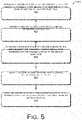
- FIG. 5is a flow diagram illustrating an example process for forming and bonding dies, according to an embodiment.
- first metallic interconnect structuresmay be bonded at ambient temperatures to second metallic interconnect structures using direct bonding techniques, which make use of the recesses in one or both of the first and second interconnect structures.
- the recessesmay be formed in the interconnect structures for this purpose, or recesses resulting from CMP (and the like) may be remedied with this innovative technique. Interconnect pads with larger surface areas and others with deeper dishing can particularly benefit.
- a method for forming a microelectronic assemblyincludes planarizing a bonding surface of a first substrate, where the first substrate includes a first metallic pad embedded into the bonding surface of the first substrate, and depositing a first material onto a surface of the first metallic pad. Also, planarizing a bonding surface of a second substrate, where the second substrate includes a second metallic pad embedded into the bonding surface of the second substrate, and depositing a second material onto a surface of the second metallic pad. Then, bonding the bonding surface of the second substrate to the bonding surface of the first substrate via direct bonding without adhesive.
- the methodincludes depositing the first material and/or the second material via immersion electroless metal deposition, or a like technique.
- the methodincludes forming a eutectic alloy mass between the first metallic pad and the second metallic pad, where the eutectic alloy mass or near eutectic composition alloy mass comprises an alloy of the first and second metallic materials.
- the methodmay include forming a first recessed portion in a surface of the first metallic pad and a second recessed portion in a surface of the second metallic pad, and at least partially filling the first recessed portion with the first material and at least partially filling the second recessed portion with the second material.
- the methodincludes depositing a conductive barrier layer onto the surface of the first metallic pad and/or the surface of the second metallic pad prior to depositing the first material or the second material, respectively.
- techniques and methodsinclude forming a microelectronic assembly, comprising a first substrate having a bonding surface with a planarized topography and a first plurality of metallic pads or traces or combinations of thereof at the bonding surface of the first substrate and a second substrate having a bonding surface with a planarized topography, which is bonded to the bonding surface of the first substrate.
- a second plurality of metallic pads at the bonding surface of the second substrateare bonded to the first plurality of metallic pads.
- the first plurality of metallic pads and/or the second plurality of metallic padsare comprised of two or more conductive materials.
- a first recessed portionis disposed in a surface of the first plurality of metallic pads that extends a preselected depth below the surface of the first plurality of metallic pads, or a preselected depth below the bonding surface of the first substrate.
- the first recessed portionis at least partially filled with a first conductive material different than a conductive material of the first plurality of metallic pads.
- a second recessed portionmay be disposed in a surface of the second plurality of metallic pads that extends a preselected depth below the surface of the second plurality of metallic pads, or a preselected depth below the bonding surface of the second substrate.
- the second recessed portionis at least partially filled with a second conductive material different than a conductive material of the second plurality of metallic pads.
- a barrier layeris disposed within the first recessed portion and/or the second recessed portion.
- the barrier layeris comprised of a third conductive material different from the first or second conductive materials and different than the conductive material of the first or second plurality of metallic pads.
- an alloy mass(e.g., a eutectic alloy mass) is disposed between the first plurality of metallic pads and the second plurality of metallic pads, where the alloy mass comprises an alloy of the first and second conductive materials.
- the region between the first plurality of metallic pads or the second plurality of metallic pads and the alloy massis non-linear.
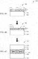
- FIGS. 1A-5illustrate representative devices, as well as processes 100 and 300 - 600 for forming and preparing various microelectronic components (such as dies 102 and assemblies 118 , for example) for bonding, such as for direct bonding without adhesive.
- the processes 100 and 300 - 600include providing a bonding surface (such as bonding surface 108 , for example) on the microelectronic components, or two bonding surfaces in some examples (not shown), providing conductive interconnect structures embedded into the bonding surfaces, repairing or mitigating erosion, dishing, and the like in the bonding surfaces due to processing or defects, forming microelectronic assemblies by directly bonding the microelectronic components at the bonding surfaces, and so forth.
- processes 100 and 300 - 600are described is not intended to be construed as limiting, and any number of the described process blocks in any of the processes 100 and 300 - 600 can be combined in any order to implement the processes or alternate processes. Additionally, individual blocks may be deleted from any of the processes without departing from the spirit and scope of the subject matter described herein. Furthermore, the processes 100 and 300 - 600 can be implemented in any suitable hardware, software, firmware, or a combination thereof, without departing from the scope of the subject matter described herein. In alternate implementations, other techniques may be included in the processes 100 and 300 - 600 in various combinations and remain within the scope of the disclosure.
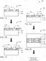
- a representative “die” 102may be formed using various techniques, to include a base substrate 104 and an insulating or dielectric layer 106 .
- the base substrate 104may be comprised of silicon, germanium, glass, quartz, a dielectric surface, direct or indirect gap semiconductor materials or layers or another suitable material.
- the insulating layer 106is deposited or formed over the substrate 104 , and may be comprised of an inorganic dielectric material layer such as oxide, nitride, oxynitride, oxycarbide, carbides, carbonitrides, diamond, diamond like materials, glasses, ceramics, glass-ceramics, and the like.
- a bonding surface 108 of the die 102can include conductive features 110 , such as conductive interconnect structures for example, embedded into the insulating layer 106 and arranged so that the conductive features 110 from respective bonding surfaces 108 can be mated and joined during bonding, if desired.
- the joined interconnect features 110can form continuous conductive interconnects (for signals, power, etc.) between stacked dies 102 .
- Damascene processesmay be used to form the embedded conductive features 110 in the insulating layer 106 .
- the conductive features 110may be comprised of metals (e.g., copper, etc.) or other conductive materials, or combinations of materials, and include structures, traces, pads, patterns, and so forth.
- the conductive features 110may be included in the insulating layer 106 to provide an electrical and/or thermal path or may instead be configured to balance out the metallization of the bonding surface 108 , through the use of additional pads or so-called dummy pads, traces, patterns or the like.
- the exposed surface of the die 102including the insulating layer 106 and the conductive features 110 can be planarized to form a flat bonding surface 108 .
- one or more bonding surfaces 108 of a die 102can be planarized (using chemical-mechanical polishing (CMP), or the like) to prepare the surface(s) 108 for bonding.
- CMPchemical-mechanical polishing
- Forming the bonding surface 108includes finishing the surface 108 to meet dielectric roughness specifications and metallic layer (e.g., copper, etc.) recess specifications, to prepare the surface 108 for direct bonding.
- the bonding surface 108is formed to be as flat and smooth as possible, with very minimal surface topology variance.
- Various conventional processes, such as chemical mechanical polishing (CMP)may be used to achieve the low surface roughness.
- This processprovides the flat, smooth surface 108 that results in a reliable bond between dies 102 .
- the exposed surface of the conductive features 110may be intentionally recessed, to allow for material expansion, particularly during heated annealing, if it is to be performed.
- the planarizingcan produce dielectric erosion (not shown) on the bonding surface 108 in areas with high metal pattern density, and dishing (i.e., recesses 112 ) in the exposed surface of metal features 110 .
- the dishing of the features 110can create a notable variance (having a depth (“d 1 ”), for example) in the overall surface topology of the die 102 .
- the topology variancemay be great enough to weaken a direct bond between dies 102 or reduce the reliability of the bond at the locations of the surface variance(s) (e.g., recesses 112 ).
- dishing or recesses 112 having a preselected depth (“d 1 ”)may be intentionally formed in the surface of a conductive feature 110 , to prepare the conductive feature 110 for low temperature (e.g., ambient, room temperature, less than 100° C.) bonding techniques, as disclosed herein.
- Intentional forming of recesses 112 at a preselected depth (“d 1 ”)may be accomplished while forming the conductive features 110 , or may be accomplished afterwards, with planarization, etching, or the like.
- the preselected depth (“d 1 ”) of the recess 112may be dependent on the surface area of the exposed portion of the conductive feature 110 .
- a conductive feature 110 with a larger surface area and/or thicker conductive layermay have or be provided with a deeper recess 112
- a conductive feature 110 with a smaller surface area and/or thinner conductive layermay have or be provided with a more shallow recess 112 .
- first metallic interconnect features 110 at a first die 102may be bonded at ambient temperatures (e.g., less than 100° C.) to second metallic interconnect features 110 at a second die 102 using direct bonding techniques, which make use of the recesses 112 in one or both of the first and second interconnect features 110 .
- the recesses 112may be formed in the interconnect features 110 for this purpose, or recesses 112 resulting from CMP (and the like) may be remedied with this innovative technique. Interconnect features 110 with larger surface areas and others with deeper dishing can particularly benefit.
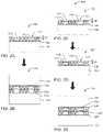
- the recess(es) 112 in the metallic interconnect features 110are filled with one or more fill layers 114 and/or one or more fill layers 116 that form a fill mass 202 (see FIGS. 1 F and 1 G) when the interconnect features 110 with the fill layers 114 , 116 are pressed together.
- the one or more fill layers 114 , 116 in each of the first and second interconnect features 110can fuse together upon intimate contact to form the fill mass 202 , which also fuses to the respective first and second interconnect features 110 , which form a unified low-temperature bonded conductive interconnect 204 .
- the fill mass 202may comprise a eutectic alloy mass or a composition close to a eutectic alloy mass.
- the one or more fill layers 114 and 116 at the respective first and second interconnect features 110fuse together to form the fill mass 202 at a comparatively lower temperature than needed to fuse the first and second interconnect features 110 (by annealing, etc.).
- the bonding temperature of the layers comprising the fill mass 202is lower than the bonding temperature of the opposing layers comprising the interconnect features 110 without the fill layers 114 or 116 .
- the melting point of the fill layer 114 and/or the fill layer 116may be lower than the melting point of the materials of one or both of the first and second interconnect features 110 .
- the materials of the one or more metal fill layers 114 , 116may be selected so that the combination of materials forms a composite or an alloy with a higher melting point than either of the fill layers 114 and 116 , and of the metal of the first and/or second interconnect features 110 .
- a first fill layer 114is formed, added, deposited, coated, or the like, on the exposed surface of the first interconnect features 110 of the first die 102 .
- the fill layer 114is formed at a preselected thickness to reduce the recess 112 from the greater depth (“d 1 ”) to a lesser depth (“d 2 ”).
- the depth (“d 2 ”)can be a desired or preselected depth, chosen for material expansion and to allow for a reliable direct bond.
- the depth (“d 2 ”)may be dependent on the materials of the first interconnect features 110 , the materials of the first fill layer 114 , the size or area of the first interconnect features 110 , the temperature and duration of the annealing process to take place, and the like.
- d 1depth
- d 2depth
- the one or more first fill layers 114may be deposited using various techniques, including spin coating, vapor coating, selective electroless plating, atomic layer deposition, or the like, onto the surface of the first interconnect features 110 .
- the first fill layer(s) 114may be continuous (as shown at FIG. 1C , at 114 ) or discontinuous (as shown at FIG. 1C at 114 ′).
- each of the multiple first fill layers 114may be discontinuous; the layers 114 may fully or partially overlap one another; or one or more of the multiple first fill layers 114 may be continuous, with other first fill layer(s) 114 being discontinuous.
- the first fill layer(s) 114may be comprised of indium, alloys of indium or a similar metal, polysilicon, or other materials.
- a discontinuous fill layer 114 ′is less likely to decrease the conductivity of the materials of a bonded structure including the fill layer 114 ,′ being a very thin layer, while still strengthening bonded material between interconnect structures 110 .
- a first fill layer 114 (continuous) or 114 ′ (discontinuous) comprised of polysiliconcan provide a harder bond surface that is less susceptible to recessing during ClVIP planarization, can have a coefficient of thermal expansion (CTE) that is similar to, and therefore more compatible to the insulating layer 106 , can be less selective to etching chemistry, and can provide a reliable direct bond, without substantially decreasing the conductivity of the conductive feature 110 or the interconnect structure 204 .
- CTEcoefficient of thermal expansion
- a second fill layer 116is formed, added, deposited, or the like, on the exposed surface of the second interconnect features 110 of the second die 102 .
- the fill layer 116can be formed at a preselected thickness to reduce the recess 112 to a desired depth (d 2 , or a depth d 2 ′ that is not necessarily identical to the depth “d 2 ” as shown at FIG. 1C ).
- the second fill layer 116may be deposited using various techniques, including spin coating, vapor coating, selective electroless plating, atomic layer deposition, or the like, onto the surface of the second interconnect features 110 .
- the second fill layer 116 on interconnect features 110 of the second die 102 or substratemay be continuous (as shown at FIG. 1D , at 116 ) or discontinuous (as shown at FIG. 1D at 116 ′).
- each of the multiple second fill layers 116may be discontinuous; the layers 116 may fully or partially overlap one another; or one or more of the multiple second fill layers 116 may be continuous, with other second fill layer(s) 116 being discontinuous.
- the second fill layer 116may be comprised of gallium, tin, their respective alloys, polysilicon, or similar materials.
- a second fill layer 116 (continuous) or 116 ′ (discontinuous) comprised of polysiliconcan provide a harder bond surface that is less susceptible to recessing during CMP planarization, can have a coefficient of thermal expansion (CTE) that is similar to, and therefore more compatible to the insulating layer 106 , can be less selective to etching chemistry, and can provide a reliable direct bond, without substantially decreasing the conductivity of the conductive feature 110 or the interconnect structure 204 .
- CTEcoefficient of thermal expansion
- first fill layer 114 and the second fill layer 116comprise different materials.
- first 114 and second 116 fill layerscomprise the same material(s).
- additional fill layersmay be added to the first 114 and/or the second 116 fill layers (either before or after deposition of the first 114 and/or second 116 fill layers).
- Either or both of fill layers 114 and 116may be a combination of two or more materials, including a combination of polysilicon and one or more metals or alloys, or the like.
- the first 114 and second 116 fill layersmay be deposited on the recessed interconnect features 110 by various means in different implementations.
- an electroless processsuch as a direct replacement reaction or an auto-catalytical metal deposition process is used to selectively deposit a metallic fill layer 114 , 116 over the recessed interconnect features 110 (e.g., copper) with precision control.
- an electroless immersion deposition processmay be used.
- such a processmay be used to deposit first 114 and second 116 fill layers of gold, silver, palladium, nickel, indium, gallium, cobalt, germanium, or any other metals, or combinations of the same, or the like.
- the processmaintains a low cost, since it uses no lithography, no vacuum, no heat, and no additional CMP is required after deposition.
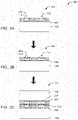
- an additional CMP stepmay be performed on one or both the dies 102 (or wafers). Since two or more recesses 112 are possible on the die 102 (or wafer) depending on the different diameters of the pads 110 , a polishing or CMP step may remove material from some pads 110 and not from others.
- the first and second dies 102are stacked and bonded using direct dielectric to dielectric bonding (without adhesive), at ambient temperature (e.g., below 100 degrees C.). This includes bringing the non-metallic regions of the prepared bonding surface 108 of each die 102 together so that the bonding surfaces 108 make contact, and bond to each other.
- the bonding of the first and second dies 102forms a microelectronic assembly 118 .
- the insulating layer 106 of a die 102is direct bonded to another insulating layer 106 of a same or similar material on another die 102 , or in some examples the other die 102 may not have a separate insulating layer 106 and the bonding happens between the insulating layer 106 of die 102 (e.g. silicon oxide) and a silicon layer, such as the base substrate 104 for example, on the other die 102 .
- the insulating layer 106 of 102e.g. silicon oxide
- a silicon layersuch as the base substrate 104 for example
- the first fill layer 114 and the second fill layer 116are pressed and bonded together, as the interconnect features 110 bond together into a solid interconnect structure 204 at a subsequent temperature, which may be lower than 200° C. and preferably lower than 170° C. or 100° C.
- the composition of the first fill layer 114 and/or the second fill layer 116is less than 25% and preferably less than 10% of the bonded conductive feature 204 .
- the intimate mating of the first fill layer 114 and the second fill layer 116may comprise thermal deformation of the fill layer 114 and/or the fill layer 116 .
- a composite comprising the materials of the interconnect features 110 and the materials of the fill layer 114 of the first die 102may bond with a composite comprising the materials of the interconnect features 110 and the materials of the fill layer 116 of the second die 102 by thermal deformation and grain boundaries diffusion processes.
- the first fill layer 114 and the second fill layer 116combine to form the fill mass 202 , which physically bonds and may also electrically bond the respective interconnect features 110 , which form the interconnect structure 204 .
- the fill mass 202comprises a region between the first and second interconnect features 110 (of the bonded interconnect 204 formed by bonding the first and second interconnect features 110 ) having a non-linear concentration of materials.
- the first fill layer 114 and the second fill layer 116combine to form the fill mass 202 , but the concentration of the first fill layer 114 to the second fill layer 116 may be non-linear throughout the fill mass 202 within the bonded interconnect structure 204 .
- the fill mass 202comprises an electrically conductive fill mass 202 joined to the first and second conductive interconnect features 110 , where the conductive fill mass 202 includes a first material comprising the material of the first interconnect feature 110 (of the first die 102 ), a second material comprising the material of the second interconnect feature 110 (of the second die 102 ), and at least a third material comprising the materials of either or both of the first fill 114 and the second fill 116 .
- the third materialcan be selected to increase the melting point of an alloy including the third material and at least one of the first material or the second material.
- the conductive fill mass 202includes a third material comprising at least the first fill 114 and a fourth material comprising at least the second fill 116 .
- the fill mass 202comprises an electrically conductive fill mass 202 joined to the first and second conductive interconnect features 110 , where the conductive fill mass 202 includes a first material comprising the material of the first fill 114 , a second material comprising the material of the second fill 116 , and at least a third material comprising an alloy or a compound of the materials of the first fill 114 and the second fill 116 .
- the third materialcan be selected by a selection of the first 114 and second 116 fills to increase the melting point of an alloy including the third material and at least one of the first material or the second material.
- the conductive fill mass 202includes one or more layers or materials (e.g., metals or other conductive materials) in addition to the materials of the first fill 114 and the second fill 116 .
- the fill mass 202comprises an electrically conductive fill mass 202 joined to the first and second conductive interconnect features 110 , where the conductive fill mass 202 includes a first material comprising a material of the first fill 114 and a second material comprising a material of the second fill 116 , where one or both of the first material and the second material comprise a polysilicon.
- the polysiliconmay be discontinuous to enhance the conductivity of the fill mass 202 , as well as the conductivity of the interconnect structure 204 .
- a concentration of the first materialcan vary from a relatively higher amount at a location disposed toward the first interconnect feature 110 (or the first die 102 ) to a relatively lower amount toward the second interconnect feature 110 (or the second die 102 ), and a concentration of the second material can vary in concentration from a relatively higher amount at a location disposed toward the second interconnect feature 110 (or the second die 102 ) to a relatively lower amount toward the first interconnect feature 110 (or the first die 102 ).
- the third material(if present) has a highest concentration at a location between a first highest concentration of the first material and a second highest concentration of the second material.
- the concentration of the first fill layer 114 or second fill layer 116 in the bonded conductive feature 204is less than 25% and preferably less than 10% of the bonded conductive feature 204 .
- materials of the first fill layer 114 or the second fill layer 116may diffuse and/or inter-diffuse into the first or second conductive features 110 during subsequent processing steps or during field use.
- the fill mass 202 formed by the first and second fill layers 114 , 116may comprise a distinct region in the bonded conductive features 204 .
- the first fill layer 114 or the second fill layer 116may diffuse into the first or second conductive features 110 , and their concentration can be more diffuse, where the local concentration of the first fill layer 114 or the second fill layer 116 is less than 5%, and preferably less than 1% of the surrounding conductive material (e.g., the material of interconnects 110 ).
- the fill mass 202is formed at low temperatures (e.g., ambient, room temperature, less than 100° C.) and provides a bond with reliable strength and conductivity without higher temperature annealing.
- the strength and reliability of the low temperature bond including the fill mass 202can be equivalent to or substantially similar to a bond formed through higher temperature annealing.
- interconnects 204 between the bonded dies 102may be formed using the low temperature fill mass 202
- at least one or more interconnects 204 between the bonded dies 102may be formed using a hybrid bonding of metal material (e.g. copper) from one interconnect 110 of a first die 102 , to metal material (e.g. copper) from another interconnect 110 of a second die 102 .
- metal materiale.g. copper
- the contact region between bonded interconnects 110may be partially formed of a combination of a fill mass 202 , a copper-to-copper bond, and even include one or more voids.
- the substrate 104 of the bottom die 102 and the substrate 104 of the top die 102may be similar or identical in geometric proportions. As shown at FIG. 1G , one or more of the substrates 104 of the bonded dies 102 (e.g., the microelectronic assembly 118 ) may be thinned as desired for further processing or packaging. In other applications, the bottom substrate 104 may be significantly larger than the top substrate 104 .
- the bottom substrate 104may be comprised of a 200 or 300 mm silicon wafer, or the like, while the top substrate 104 may be comprised of a die 102 that is significantly smaller than the bottom substrate 104 .
- Multiple dies 102may be bonded to the planarized bonding surface 108 of the bottom die 102 .
- the bonded dies 102may be processed for additional bonding operations, for example, stacking other cleaned dies 102 to the initially bonded dies 102 , and so forth.
- the bottom larger substrate 104may be further processed, for example, thinning or singulation operations or both, to separate the various bonded dies 102 for subsequent operations.
- the techniques described hereincan be used to remedy or mitigate the effects of unintentionally recessed interconnect structures in the surfaces of microelectronic components to be bonded.
- At least partially filling the excessive recesses 112 in the interconnect features 110 with the one or more additional fill layers ( 114 , 116 )provides for an improved bonding surface (e.g., less surface topology variance).
- an improved bonding surfacee.g., less surface topology variance.
- Direct and hybrid bonding with the improved surface flatnesscan result in improved and more reliable bonds between the microelectronic components (e.g., dies 102 ).
- improved bonds between the interconnect features 110 of the respective dies 102is achievable with lower temperatures due to the fill mass 202 formed at the bond joint.
- recesses 112may be intentionally formed in the exposed surfaces of one or more of the interconnect features 110 to be bonded, to apply the techniques described. For example, either of these scenarios can be illustrated with regard to the process 300 of FIGS. 2A-2E .
- the process 300includes forming the conductive features 110 in the insulating layer 106 using a damascene process, for instance.
- a recess 112 of predetermined size and shapee.g., area and depth “d 1 ”
- portions of conductive features 110may be selectively partially removed with respect to the bonding surface of dielectric 106 to a predetermined depth by etching methods, or the like.
- the recess 112can be intentionally created by patterning and etching the features 110 , for example.
- a photoresistcan be applied (not shown) to the feature 110 surface to pattern the feature 110 for predetermined recess 112 locations.
- the resistcan be exposed and then the surface of the feature 110 etched to form the desired recess(es) 112 .
- the predetermined recesses 112can have a depth “d 1 ” of tens of nanometers to hundreds of nanometers (e.g., 50 to 500 nm), or even deeper as desired.
- the recess 112can be created by CMP, or the like, for example when the recess 112 is formed on a large metallic feature 110 during planarization, as described above.
- the depth “d 1 ” of the recess 112can be greater than 15 nm.
- bonding the two dies 102 to form the microelectronic assembly 118 without mitigating the recesses 112can leave voids or gaps 302 between the features 110 .
- the gaps 302comprise massive defects in the bonds, and can prevent the interconnect structures 204 from being formed, or from being reliably formed from the respective features 110 .
- the massive defects from the gaps 302can result in premature failure or low device yield.
- the process 300includes adding one or more fill layers 114 , 116 , as described above to mitigate the recess(es) 112 and the gaps 302 .
- one or more first fill layers 114 or 114 ′are formed, added, deposited, coated, or the like, on the exposed surface of the first interconnect features 110 of the first die 102 , as described above.
- one or more second fill layers 116 or 116 ′are formed, added, deposited, or the like, on the exposed surface of the second interconnect features 110 of the second die 102 , as described above.
- the first and second dies 102are bonded using direct dielectric to dielectric bonding (without adhesive), at room temperature (e.g., below 100 degrees C.).
- the bonding of the first and second dies 102forms a microelectronic assembly 118 .
- the first fill layer(s) 114 and the second fill layer(s) 116are pressed and bonded together, and the interconnect features 110 are bonded into a solid interconnect structure 204 , with the first fill layers 114 and the second fill layers 116 combining to form an fill mass 202 , which physically bonds and may also electrically bond the respective interconnect features 110 , which form the interconnect structure 204 .
- the composition of the fill mass 202may comprise a eutectic alloy or a composition close to a eutectic alloy mass.
- a small gapmay remain within the fill mass 202 after bonding (not shown). If the gap is small, it may be inconsequential. However, if the gap is large, it may lead to failures. In that case, the thickness of one or both of the first 114 and/or second 116 fill layers can be increased prior to bonding. Alternately, one or more additional fill layers can be added (additional to the first 114 and second 116 fill layers) prior to bonding to reduce or eliminate the gap.
- the fill mass 202has a non-linear concentration of materials, as described above.
- a concentration of the material of the first fill 114can vary from a relatively higher amount at a location disposed toward the first interconnect feature 110 (or the first die 102 ) to a relatively lower amount toward the second interconnect feature 110 (or the second die 102 )
- a concentration of the material of the second fillcan vary in concentration from a relatively higher amount at a location disposed toward the second interconnect feature 110 (or the second die 102 ) to a relatively lower amount toward the first interconnect feature 110 (or the first die 102 ).
- a third materialcomprising an alloy or compound of the first 114 and second 116 materials has a highest concentration within the fill mass 202 at a location between a first highest concentration of the first material and a second highest concentration of the second material.
- the fill mass 202is formed at low temperatures (e.g., ambient, room temperature, less than 150° C.) and provides a bond with reliable strength and adequate conductivity.
- the strength of the low temperature bond including the fill mass 202is equivalent to or substantially similar to a bond formed through higher temperature annealing.
- FIGS. 3A-3Ca process 400 is shown as an alternate implementation of the process 300 .
- FIGS. 3A, 3B, and 3Cmay be inserted as additional or alternate process steps for the process 300 .
- barrier layers 402 and/or 404(such as nickel, nickel alloys or the like) are deposited onto the recess 112 of one or both dies 102 prior to the first 114 and/or second 116 fill layers.
- the first 114 and second 116 fill layersare mated intimately, and form the fill mass 202 as described above.
- the barrier layers 402 and/or 404may or may not combine with the fill layers 114 , 116 and/or feature 110 materials to become part of the fill mass 202 .
- FIGS. 4A-4Cshow a process 500 illustrating the use of electroless metal deposition, as a technique for forming the first fill layer 114 and/or the second fill layer 116 .
- the process 500may be particularly useful in cases where the recess 112 may be particularly deep (e.g., “d 1 ”>50 nm).
- FIG. 4Aillustrates a die 102 with an excessively deep recess 112 , either intentionally or unintentionally (e.g., CMP planarization).
- the excessively deep recess 112can be due to one of the dimensions of the recess 112 , for example (e.g., greater than 0.05 mm) or the large size of the surface area of the features 110 .
- an electroless processsuch as direct replacement reaction or auto-catalytical metal deposition, for instance, is used to selectively deposit the fill layer 114 onto the exposed surface of the conductive feature 110 with precision control.
- the fill layer 114is deposited at a preselected thickness to reduce the recess 112 to a predetermined depth (“d 2 ”) as desired, to meet direct bonding requirements.
- the electroless processcomprises an immersion silver, copper, or gold process.
- a seed deposition of palladiumfor example, is followed by a deposition of nickel, or the like.
- the nickel depositionmay be made by a hypophosphite-based immersion process, after depositing the seed layer.
- the reducing agent for the immersion processincludes one or more of sodium hypophosphite, sodium borohydride, dimethylamine borane, hydrazine, or the like.
- the electroless deposition techniquehas several advantages, including the lack of a need for lithography, no vacuum or heat is used, and no additional CMP is required after deposition. Other advantages will also be apparent to a person having skill in the art.
- a fill layer 114 of polysilicon, or a combination of polysilicon and another material, such as a metal,may be deposited within the recess 112 to reduce the depth of the recess 112 .
- two of the dies 102 with the fill layers 114are bonded together to form the microelectronic assembly 118 .
- the fill layers 114form a fill mass 202 , which bonds (at low temperatures) with the conductive features 110 to form a solid interconnect structure 204 .
- FIG. 5is a flow diagram illustrating an example process 600 for forming and bonding microelectronic components (such as dies 102 , for example), according to an embodiment.
- the processincludes planarizing a bonding surface (such as the bonding surface 108 , for example) of a first substrate (such as a first die 102 , for example).
- the first substrateincludes a first metallic pad (such as conductive feature 110 , for example) embedded into the bonding surface of the first substrate.
- the processincludes depositing one or more first materials (such as first fill layer(s) 114 , for example) onto a surface of the first metallic pad.
- the processincludes forming a first recessed portion (such as recess 112 , for example) in a surface of the first metallic pad and at least partially filling the first recessed portion with the first material(s).
- the recessis the product of one or more process steps, and may be intentional or unintentional.
- the processincludes depositing a conductive barrier layer (such as barrier 402 , for example) onto the surface of the first metallic pad prior to depositing the first material(s).
- a conductive barrier layersuch as barrier 402 , for example
- the processincludes depositing multiple fill layers, barrier layers, or combinations of the same.
- the processincludes planarizing a bonding surface of a second substrate (such as a second die 102 , for example).
- the second substrateincludes a second metallic pad embedded into the bonding surface of the second substrate.
- the processincludes depositing one or more second materials (such as second fill layer(s) 116 , for example) onto a surface of the second metallic pad.
- the processincludes forming a second recessed portion in a surface of the second metallic pad and at least partially filling the second recessed portion with the second material(s).
- the recessis the product of one or more process steps, and may be intentional or unintentional.
- the processincludes depositing a conductive barrier layer (such as barrier layer 404 , for example) onto the surface of the second metallic pad prior to depositing the second material(s).
- a conductive barrier layersuch as barrier layer 404 , for example
- the processincludes depositing multiple fill layers, barrier layers, or combinations of the same.
- the processincludes depositing the first material and/or the second material via immersion electroless metal deposition.
- the melting point of the first fill layer and/or the second fill layermay be higher than the melting point of the conductive features 110 .
- the first fill layer(s) and/or the second fill layer(s)may be comprised of a very thin layer of nickel, cobalt, or manganese, or their various alloys, while the conductive features may be comprised of copper or of copper alloys, for example.
- one or more of the first fill layer(s) and/or one or more of the second fill layer(s)may be comprised of polysilicon.
- the deposited first fill layer(s) and/or the second fill layer(s)may be continuous or discontinuous, and the thickness of the first fill layer(s) and/or the second fill layer(s) may range between 0.5 to 500 nm, and preferably between 1 to less than 50 nm.
- the first fill layer(s) and/or the second fill layer(s)may be comprised of an alloy of at least one higher-temperature melting point metal and at least one lower-temperature melting point metal, for example, a cobalt-tin or cobalt-indium alloy, or the like, or an element with a relatively low concentration of one or more impurities.
- the composition of the alloy or elementmay include a proportion of the fill material (or impurities) that is less than 2% of the total composition of the interconnect pads combined, or less than 5000 ppm, or less than 500 ppm.
- first fill layer(s) and/or the second fill layer(s)are thinner than the respective conductive feature. In one application, the first fill layer(s) and/or the second fill layer(s) are at least 5 times thinner than the thickness of the respective conductive feature.
- the processincludes bonding the bonding surface of the second substrate to the bonding surface of the first substrate via direct dielectric-to-dielectric bonding without adhesive.
- the processincludes pressing the first metallic pad to the second metallic pad during the bonding, and pressing the first fill layer to the second fill layer to form a fill mass (such as fill mass 204 , for example) between the first metallic pad and the second metallic pad.
- the fill masscan comprise an alloy of the first and second fill materials.
- the processincludes bonding the second metallic pad to the first metallic pad via the fill mass, to form a single solid interconnect structure (such as interconnect structure 204 , for example).
- a concentration of the first fill material and a concentration of the second fill material of the fill massis non-linear throughout the fill mass.
- the bonded substratecan include a portion having a conductive interconnect structure comprised of mostly copper, for example, and another portion having an interconnect structure including an fill mass (for example, a copper-cobalt alloy mass or a metal-polysilicon mass) comprised of the conductive feature (e.g., copper) and one or more fill layer (e.g., cobalt, polysilicon, etc.).
- an fill massfor example, a copper-cobalt alloy mass or a metal-polysilicon mass
- process stepsmay be modified or eliminated, in comparison to the process steps described herein.
Landscapes
- Engineering & Computer Science (AREA)
- Microelectronics & Electronic Packaging (AREA)
- Power Engineering (AREA)
- Computer Hardware Design (AREA)
- Manufacturing & Machinery (AREA)
- Physics & Mathematics (AREA)
- Condensed Matter Physics & Semiconductors (AREA)
- General Physics & Mathematics (AREA)
- Internal Circuitry In Semiconductor Integrated Circuit Devices (AREA)
Abstract
Description
- This application is a Continuation of U.S. patent application Ser. No. 16/655,002, filed Oct. 16, 2019, which is a Continuation-in-Part of U.S. patent application Ser. No. 16/363,894, filed Mar. 25, 2019, now U.S. Pat. No. 10,790,262, which claims the benefit under 35 U.S.C. § 119(e)(1) of U.S. Provisional Application No. 62/656,264, filed Apr. 11, 2018, all of which are hereby incorporated by reference in their entirety.
- The following description relates to integrated circuits (“ICs”). More particularly, the following description relates to manufacturing IC dies and wafers.
- Microelectronic elements often comprise a thin slab of a semiconductor material, such as silicon or gallium arsenide, commonly called a semiconductor wafer. A wafer can be formed to include multiple integrated chips or dies on a surface of the wafer and/or partly embedded within the wafer. Dies that are separated from a wafer are commonly provided as individual, prepackaged units. In some package designs, the die is mounted to a substrate or a chip carrier, which is in turn mounted on a circuit panel, such as a printed circuit board (PCB). For example, many dies are provided in packages suitable for surface mounting.
- Packaged semiconductor dies can also be provided in “stacked” arrangements, wherein one package is provided, for example, on a circuit board or other carrier, and another package is mounted on top of the first package. These arrangements can allow a number of different dies to be mounted within a single footprint on a circuit board and can further facilitate high-speed operation by providing a short interconnection between the packages. Often, this interconnect distance can be only slightly larger than the thickness of the die itself. For interconnection to be achieved within a stack of die packages, interconnection structures for mechanical and electrical connection may be provided on both sides (e.g., faces) of each die package (except for the topmost package).
- Additionally, dies or wafers may be stacked in a three-dimensional arrangement as part of various microelectronic packaging schemes. This can include stacking a layer of one or more dies, devices, and/or wafers on a larger base die, device, wafer, substrate, or the like, stacking multiple dies or wafers in a vertical or horizontal arrangement, and various combinations of both. Dies or wafers may be bonded in a stacked arrangement using various bonding techniques, including direct dielectric bonding, non-adhesive techniques, such as ZiBond® or a hybrid bonding technique, such as DBI®, both available from Invensas Bonding Technologies, Inc. (formerly Ziptronix, Inc.), an Xperi company (see for example, U.S. Pat. Nos. 6,864,585 and 7,485,968, which are incorporated herein in their entirety).
- There can be a variety of challenges to implementing stacked die and wafer arrangements. When bonding stacked dies using a direct bonding or hybrid bonding technique, it is usually desirable that the surfaces of the dies to be bonded be extremely flat, smooth, and clean. For instance, in general, the surfaces should have a very low variance in surface topology (i.e., nanometer scale variance), so that the surfaces can be closely mated to form a lasting bond.
- However, some processing techniques, such as chemical-mechanical polishing (CMP) and the like, which are used to prepare the bonding surfaces can also contribute to forming uneven bonding surfaces, particularly when the bonding surfaces include varying materials of varying densities. For instance, embedded metallic structures at the bonding surface can be excessively recessed during bonding surface polishing, and to a greater degree when the metallic structures have large exposed surface areas.
- Further, it can be desirable to bond the embedded metallic structures of adjacent stacked dies to form conductive interconnects between the dies. Generally, the metallic structures are bonded using heated annealing techniques to form diffusion bonds. However, the temperatures used to perform the annealing techniques can often be too great for some desirable packaging schemes or components or at least one or more materials in the package, thus limiting the types of schemes and components or combination of materials that may take advantage of these techniques.
- The detailed description is set forth with reference to the accompanying figures. In the figures, the left-most digit(s) of a reference number identifies the figure in which the reference number first appears. The use of the same reference numbers in different figures indicates similar or identical items.
- For this discussion, the devices and systems illustrated in the figures are shown as having a multiplicity of components. Various implementations of devices and/or systems, as described herein, may include fewer components and remain within the scope of the disclosure. Alternatively, other implementations of devices and/or systems may include additional components, or various combinations of the described components, and remain within the scope of the disclosure.
FIGS. 1A-1G include a graphical flow diagram illustrating an example process for forming and bonding dies, according to an embodiment.FIGS. 2A-2E include a graphical flow diagram illustrating another example process for forming and bonding dies, according to an embodiment.FIGS. 3A-3C include a graphical flow diagram illustrating an alternate example process for forming and bonding dies, according to an embodiment.FIGS. 4A-4C include a graphical flow diagram illustrating another example process for forming and bonding dies, according to an embodiment.FIG. 5 is a flow diagram illustrating an example process for forming and bonding dies, according to an embodiment.- Representative techniques and devices are disclosed, including process steps for making use of recesses in interconnect structures to form reliable low temperature conductive (e.g., hybrid) bonds. In various implementations, first metallic interconnect structures may be bonded at ambient temperatures to second metallic interconnect structures using direct bonding techniques, which make use of the recesses in one or both of the first and second interconnect structures. The recesses may be formed in the interconnect structures for this purpose, or recesses resulting from CMP (and the like) may be remedied with this innovative technique. Interconnect pads with larger surface areas and others with deeper dishing can particularly benefit.
- In various implementations, a method for forming a microelectronic assembly includes planarizing a bonding surface of a first substrate, where the first substrate includes a first metallic pad embedded into the bonding surface of the first substrate, and depositing a first material onto a surface of the first metallic pad. Also, planarizing a bonding surface of a second substrate, where the second substrate includes a second metallic pad embedded into the bonding surface of the second substrate, and depositing a second material onto a surface of the second metallic pad. Then, bonding the bonding surface of the second substrate to the bonding surface of the first substrate via direct bonding without adhesive.
- In an implementation, the method includes depositing the first material and/or the second material via immersion electroless metal deposition, or a like technique. In another implementation, the method includes forming a eutectic alloy mass between the first metallic pad and the second metallic pad, where the eutectic alloy mass or near eutectic composition alloy mass comprises an alloy of the first and second metallic materials.
- The method may include forming a first recessed portion in a surface of the first metallic pad and a second recessed portion in a surface of the second metallic pad, and at least partially filling the first recessed portion with the first material and at least partially filling the second recessed portion with the second material. In some embodiments, the method includes depositing a conductive barrier layer onto the surface of the first metallic pad and/or the surface of the second metallic pad prior to depositing the first material or the second material, respectively.
- In additional implementations, techniques and methods include forming a microelectronic assembly, comprising a first substrate having a bonding surface with a planarized topography and a first plurality of metallic pads or traces or combinations of thereof at the bonding surface of the first substrate and a second substrate having a bonding surface with a planarized topography, which is bonded to the bonding surface of the first substrate. A second plurality of metallic pads at the bonding surface of the second substrate are bonded to the first plurality of metallic pads. The first plurality of metallic pads and/or the second plurality of metallic pads are comprised of two or more conductive materials.
- In some implementations, a first recessed portion is disposed in a surface of the first plurality of metallic pads that extends a preselected depth below the surface of the first plurality of metallic pads, or a preselected depth below the bonding surface of the first substrate. The first recessed portion is at least partially filled with a first conductive material different than a conductive material of the first plurality of metallic pads. Further, a second recessed portion may be disposed in a surface of the second plurality of metallic pads that extends a preselected depth below the surface of the second plurality of metallic pads, or a preselected depth below the bonding surface of the second substrate. The second recessed portion is at least partially filled with a second conductive material different than a conductive material of the second plurality of metallic pads.
- In an alternate implementation, a barrier layer is disposed within the first recessed portion and/or the second recessed portion. The barrier layer is comprised of a third conductive material different from the first or second conductive materials and different than the conductive material of the first or second plurality of metallic pads.
- In some implementations, an alloy mass (e.g., a eutectic alloy mass) is disposed between the first plurality of metallic pads and the second plurality of metallic pads, where the alloy mass comprises an alloy of the first and second conductive materials. In some examples, the region between the first plurality of metallic pads or the second plurality of metallic pads and the alloy mass is non-linear.
- Various implementations and arrangements are discussed with reference to electrical and electronics components and varied carriers. While specific components (i.e., dies, wafers, integrated circuit (IC) chip dies, substrates, etc.) are mentioned, this is not intended to be limiting, and is for ease of discussion and illustrative convenience. The techniques and devices discussed with reference to a wafer, die, substrate, or the like, are applicable to any type or number of electrical components, circuits (e.g., integrated circuits (IC), mixed circuits, ASICS, memory devices, processors, etc.), groups of components, packaged components, structures (e.g., wafers, panels, boards, PCBs, etc.), and the like, that may be coupled to interface with each other, with external circuits, systems, carriers, and the like. Each of these different components, circuits, groups, packages, structures, and the like, can be generically referred to as a “microelectronic component.” For simplicity, unless otherwise specified, components being bonded to another component will be referred to herein as a “die.”
- This summary is not intended to give a full description. Implementations are explained in more detail below using a plurality of examples. Although various implementations and examples are discussed here and below, further implementations and examples may be possible by combining the features and elements of individual implementations and examples.
FIGS. 1A-5 illustrate representative devices, as well asprocesses 100 and300-600 for forming and preparing various microelectronic components (such as dies102 andassemblies 118, for example) for bonding, such as for direct bonding without adhesive. Theprocesses 100 and300-600 include providing a bonding surface (such asbonding surface 108, for example) on the microelectronic components, or two bonding surfaces in some examples (not shown), providing conductive interconnect structures embedded into the bonding surfaces, repairing or mitigating erosion, dishing, and the like in the bonding surfaces due to processing or defects, forming microelectronic assemblies by directly bonding the microelectronic components at the bonding surfaces, and so forth.- The order in which the
processes 100 and300-600 are described is not intended to be construed as limiting, and any number of the described process blocks in any of theprocesses 100 and300-600 can be combined in any order to implement the processes or alternate processes. Additionally, individual blocks may be deleted from any of the processes without departing from the spirit and scope of the subject matter described herein. Furthermore, theprocesses 100 and300-600 can be implemented in any suitable hardware, software, firmware, or a combination thereof, without departing from the scope of the subject matter described herein. In alternate implementations, other techniques may be included in theprocesses 100 and300-600 in various combinations and remain within the scope of the disclosure. - Referring to
FIG. 1A , a representative “die”102 may be formed using various techniques, to include abase substrate 104 and an insulating ordielectric layer 106. Thebase substrate 104 may be comprised of silicon, germanium, glass, quartz, a dielectric surface, direct or indirect gap semiconductor materials or layers or another suitable material. The insulatinglayer 106 is deposited or formed over thesubstrate 104, and may be comprised of an inorganic dielectric material layer such as oxide, nitride, oxynitride, oxycarbide, carbides, carbonitrides, diamond, diamond like materials, glasses, ceramics, glass-ceramics, and the like. - A
bonding surface 108 of thedie 102 can includeconductive features 110, such as conductive interconnect structures for example, embedded into the insulatinglayer 106 and arranged so that theconductive features 110 fromrespective bonding surfaces 108 can be mated and joined during bonding, if desired. The joined interconnect features110 can form continuous conductive interconnects (for signals, power, etc.) between stacked dies102. - Damascene processes (or the like) may be used to form the embedded
conductive features 110 in the insulatinglayer 106. The conductive features110 may be comprised of metals (e.g., copper, etc.) or other conductive materials, or combinations of materials, and include structures, traces, pads, patterns, and so forth. The conductive features110 may be included in the insulatinglayer 106 to provide an electrical and/or thermal path or may instead be configured to balance out the metallization of thebonding surface 108, through the use of additional pads or so-called dummy pads, traces, patterns or the like. After theconductive features 110 are formed, the exposed surface of thedie 102, including the insulatinglayer 106 and theconductive features 110 can be planarized to form aflat bonding surface 108. - As shown at
FIG. 1A , one ormore bonding surfaces 108 of adie 102, including embeddedinterconnect structures 110, can be planarized (using chemical-mechanical polishing (CMP), or the like) to prepare the surface(s)108 for bonding. Forming thebonding surface 108 includes finishing thesurface 108 to meet dielectric roughness specifications and metallic layer (e.g., copper, etc.) recess specifications, to prepare thesurface 108 for direct bonding. In other words, thebonding surface 108 is formed to be as flat and smooth as possible, with very minimal surface topology variance. Various conventional processes, such as chemical mechanical polishing (CMP) may be used to achieve the low surface roughness. This process provides the flat,smooth surface 108 that results in a reliable bond between dies102. In some cases, the exposed surface of theconductive features 110 may be intentionally recessed, to allow for material expansion, particularly during heated annealing, if it is to be performed. - As shown in
FIG. 1B , as a result of the discontinuity in the properties (difference in mechanical properties, polishing rates, etc.) of the material (e.g., metal, etc.) of the interconnect features110 and the dielectric material of the insulatinglayer 106, and their respective interactions with the polishing pad, its hardness, polishing slurry, and other process parameters, the planarizing can produce dielectric erosion (not shown) on thebonding surface 108 in areas with high metal pattern density, and dishing (i.e., recesses112) in the exposed surface of metal features110. In general, the higher the metal pattern density on thesurface 108, the greater the erosion, and similarly, the larger the area of the surface of the metal features110, the greater (i.e., deeper) therecesses 112. As shown atFIG. 1B , the dishing of thefeatures 110 can create a notable variance (having a depth (“d1”), for example) in the overall surface topology of thedie 102. In some cases, the topology variance may be great enough to weaken a direct bond between dies102 or reduce the reliability of the bond at the locations of the surface variance(s) (e.g., recesses112). - Among the consequences of
excessive recesses 112 on the exposed surface of interconnect features110 is poor flatness of the surface of the interconnect features110 and much higher temperatures typically needed to form continuous conductive interconnections between the metal features110 of the dies102 than the lower temperatures often desired. Withconductive features 110 having very large area pads, recesses112 can be too deep with respect to the opposing interconnect features to mate intimately without undesirable voiding defects, as the metal may not expand enough at annealing temperatures to form a bonded continuous conductive layer. Thus, the poor flatness on the surface of theconductive features 110 often produces defective bonds, when the surface is bonded or attached to other devices or substrates. - However, in various embodiments, dishing or
recesses 112 having a preselected depth (“d1”) may be intentionally formed in the surface of aconductive feature 110, to prepare theconductive feature 110 for low temperature (e.g., ambient, room temperature, less than 100° C.) bonding techniques, as disclosed herein. Intentional forming ofrecesses 112 at a preselected depth (“d1”) may be accomplished while forming theconductive features 110, or may be accomplished afterwards, with planarization, etching, or the like. In some embodiments, the preselected depth (“d1”) of therecess 112 may be dependent on the surface area of the exposed portion of theconductive feature 110. For instance, aconductive feature 110 with a larger surface area and/or thicker conductive layer may have or be provided with adeeper recess 112, and aconductive feature 110 with a smaller surface area and/or thinner conductive layer may have or be provided with a moreshallow recess 112. - Techniques and devices include process steps that make use of
recesses 112 in interconnect features110 to form reliable low temperature conductive bonds. In the implementations, first metallic interconnect features110 at afirst die 102 may be bonded at ambient temperatures (e.g., less than 100° C.) to second metallic interconnect features110 at asecond die 102 using direct bonding techniques, which make use of therecesses 112 in one or both of the first and second interconnect features110. Therecesses 112 may be formed in the interconnect features110 for this purpose, or recesses112 resulting from CMP (and the like) may be remedied with this innovative technique. Interconnect features110 with larger surface areas and others with deeper dishing can particularly benefit. - Referring to
FIGS. 1C and 1D , in an implementation, the recess(es)112 in the metallic interconnect features110 are filled with one ormore fill layers 114 and/or one ormore fill layers 116 that form a fill mass202 (see FIGS.1F and1G) when the interconnect features110 with the fill layers114,116 are pressed together. In other words, in some embodiments, the one or more fill layers114,116 in each of the first and second interconnect features110 can fuse together upon intimate contact to form thefill mass 202, which also fuses to the respective first and second interconnect features110, which form a unified low-temperature bondedconductive interconnect 204. In some embodiments, thefill mass 202 may comprise a eutectic alloy mass or a composition close to a eutectic alloy mass. - In an embodiment, the one or
more fill layers fill mass 202 at a comparatively lower temperature than needed to fuse the first and second interconnect features110 (by annealing, etc.). The bonding temperature of the layers comprising the fill mass202 (including fill layers114 and116) is lower than the bonding temperature of the opposing layers comprising the interconnect features110 without the fill layers114 or116. In some embodiments, the melting point of thefill layer 114 and/or thefill layer 116 may be lower than the melting point of the materials of one or both of the first and second interconnect features110. In other embodiments, the materials of the one or more metal filllayers - For instance, as shown at
FIG. 1C , afirst fill layer 114 is formed, added, deposited, coated, or the like, on the exposed surface of the first interconnect features110 of thefirst die 102. Thefill layer 114 is formed at a preselected thickness to reduce therecess 112 from the greater depth (“d1”) to a lesser depth (“d2”). For example, the depth (“d2”) can be a desired or preselected depth, chosen for material expansion and to allow for a reliable direct bond. In various embodiments, the depth (“d2”) may be dependent on the materials of the first interconnect features110, the materials of thefirst fill layer 114, the size or area of the first interconnect features110, the temperature and duration of the annealing process to take place, and the like. - Although only one depth (“d1”) is shown at
FIG. 1B , indicating only one recess depth, two or more such depths are also possible on thesame die 102 depending on the size of the pads of the first interconnect features110, or other reasons as mentioned earlier. Adding the fill layers114 and116 can also form two or more corresponding depths (“d2”) at thesame die 102 as well. - In various implementations, the one or more first fill layers114 may be deposited using various techniques, including spin coating, vapor coating, selective electroless plating, atomic layer deposition, or the like, onto the surface of the first interconnect features110. Also, the first fill layer(s)114 may be continuous (as shown at
FIG. 1C , at114) or discontinuous (as shown atFIG. 1C at114′). In the case of multiple first fill layers114: each of the multiple first fill layers114 may be discontinuous; thelayers 114 may fully or partially overlap one another; or one or more of the multiple first fill layers114 may be continuous, with other first fill layer(s)114 being discontinuous. - In various embodiments, the first fill layer(s)114 may be comprised of indium, alloys of indium or a similar metal, polysilicon, or other materials. A
discontinuous fill layer 114′ is less likely to decrease the conductivity of the materials of a bonded structure including thefill layer 114,′ being a very thin layer, while still strengthening bonded material betweeninterconnect structures 110. Additionally, a first fill layer114 (continuous) or114′ (discontinuous) comprised of polysilicon can provide a harder bond surface that is less susceptible to recessing during ClVIP planarization, can have a coefficient of thermal expansion (CTE) that is similar to, and therefore more compatible to the insulatinglayer 106, can be less selective to etching chemistry, and can provide a reliable direct bond, without substantially decreasing the conductivity of theconductive feature 110 or theinterconnect structure 204. - As shown at
FIG. 1D , asecond fill layer 116 is formed, added, deposited, or the like, on the exposed surface of the second interconnect features110 of thesecond die 102. As previously, thefill layer 116 can be formed at a preselected thickness to reduce therecess 112 to a desired depth (d2, or a depth d2′ that is not necessarily identical to the depth “d2” as shown atFIG. 1C ). In an embodiment, thesecond fill layer 116 may be deposited using various techniques, including spin coating, vapor coating, selective electroless plating, atomic layer deposition, or the like, onto the surface of the second interconnect features110. Also similarly, thesecond fill layer 116 on interconnect features110 of thesecond die 102 or substrate may be continuous (as shown atFIG. 1D , at116) or discontinuous (as shown atFIG. 1D at116′). In the case of multiple second fill layers116: each of the multiple second fill layers116 may be discontinuous; thelayers 116 may fully or partially overlap one another; or one or more of the multiple second fill layers116 may be continuous, with other second fill layer(s)116 being discontinuous. - In various embodiments, the
second fill layer 116 may be comprised of gallium, tin, their respective alloys, polysilicon, or similar materials. Similarly to above, a second fill layer116 (continuous) or116′ (discontinuous) comprised of polysilicon can provide a harder bond surface that is less susceptible to recessing during CMP planarization, can have a coefficient of thermal expansion (CTE) that is similar to, and therefore more compatible to the insulatinglayer 106, can be less selective to etching chemistry, and can provide a reliable direct bond, without substantially decreasing the conductivity of theconductive feature 110 or theinterconnect structure 204. - In some embodiments, the
first fill layer 114 and thesecond fill layer 116 comprise different materials. However, in an alternate embodiment, the first114 and second116 fill layers comprise the same material(s). In some alternate embodiments, additional fill layers (not shown) may be added to the first114 and/or the second116 fill layers (either before or after deposition of the first114 and/or second116 fill layers). Either or both offill layers - The first114 and second116 fill layers may be deposited on the recessed interconnect features110 by various means in different implementations. In one implementation, an electroless process, such as a direct replacement reaction or an auto-catalytical metal deposition process is used to selectively deposit a
metallic fill layer - In another embodiment, an additional CMP step may be performed on one or both the dies102 (or wafers). Since two or
more recesses 112 are possible on the die102 (or wafer) depending on the different diameters of thepads 110, a polishing or CMP step may remove material from somepads 110 and not from others. - As shown at
FIG. 1E , the first and second dies102 are stacked and bonded using direct dielectric to dielectric bonding (without adhesive), at ambient temperature (e.g., below 100 degrees C.). This includes bringing the non-metallic regions of theprepared bonding surface 108 of each die102 together so that the bonding surfaces108 make contact, and bond to each other. The bonding of the first and second dies102 forms amicroelectronic assembly 118. In alternate embodiments, the insulatinglayer 106 of adie 102 is direct bonded to another insulatinglayer 106 of a same or similar material on anotherdie 102, or in some examples theother die 102 may not have a separate insulatinglayer 106 and the bonding happens between the insulatinglayer 106 of die102 (e.g. silicon oxide) and a silicon layer, such as thebase substrate 104 for example, on theother die 102. - In the process, the
first fill layer 114 and thesecond fill layer 116 are pressed and bonded together, as the interconnect features110 bond together into asolid interconnect structure 204 at a subsequent temperature, which may be lower than 200° C. and preferably lower than 170° C. or 100° C. In one embodiment, the composition of thefirst fill layer 114 and/or thesecond fill layer 116 is less than 25% and preferably less than 10% of the bondedconductive feature 204. In some embodiments, the intimate mating of thefirst fill layer 114 and thesecond fill layer 116 may comprise thermal deformation of thefill layer 114 and/or thefill layer 116. In other applications, a composite comprising the materials of the interconnect features110 and the materials of thefill layer 114 of thefirst die 102 may bond with a composite comprising the materials of the interconnect features110 and the materials of thefill layer 116 of thesecond die 102 by thermal deformation and grain boundaries diffusion processes. - As shown at
FIG. 1F , thefirst fill layer 114 and thesecond fill layer 116 combine to form thefill mass 202, which physically bonds and may also electrically bond the respective interconnect features110, which form theinterconnect structure 204. In various embodiments, thefill mass 202 comprises a region between the first and second interconnect features110 (of the bondedinterconnect 204 formed by bonding the first and second interconnect features110) having a non-linear concentration of materials. In other words, thefirst fill layer 114 and thesecond fill layer 116 combine to form thefill mass 202, but the concentration of thefirst fill layer 114 to thesecond fill layer 116 may be non-linear throughout thefill mass 202 within the bondedinterconnect structure 204. - In some embodiments, the
fill mass 202 comprises an electricallyconductive fill mass 202 joined to the first and second conductive interconnect features110, where theconductive fill mass 202 includes a first material comprising the material of the first interconnect feature110 (of the first die102), a second material comprising the material of the second interconnect feature110 (of the second die102), and at least a third material comprising the materials of either or both of thefirst fill 114 and thesecond fill 116. In an embodiment, the third material can be selected to increase the melting point of an alloy including the third material and at least one of the first material or the second material. In various embodiments, theconductive fill mass 202 includes a third material comprising at least thefirst fill 114 and a fourth material comprising at least thesecond fill 116. - In other embodiments, the
fill mass 202 comprises an electricallyconductive fill mass 202 joined to the first and second conductive interconnect features110, where theconductive fill mass 202 includes a first material comprising the material of thefirst fill 114, a second material comprising the material of thesecond fill 116, and at least a third material comprising an alloy or a compound of the materials of thefirst fill 114 and thesecond fill 116. In the embodiments, the third material can be selected by a selection of the first114 and second116 fills to increase the melting point of an alloy including the third material and at least one of the first material or the second material. In various embodiments, theconductive fill mass 202 includes one or more layers or materials (e.g., metals or other conductive materials) in addition to the materials of thefirst fill 114 and thesecond fill 116. - In further embodiments, the
fill mass 202 comprises an electricallyconductive fill mass 202 joined to the first and second conductive interconnect features110, where theconductive fill mass 202 includes a first material comprising a material of thefirst fill 114 and a second material comprising a material of thesecond fill 116, where one or both of the first material and the second material comprise a polysilicon. In the embodiments, the polysilicon may be discontinuous to enhance the conductivity of thefill mass 202, as well as the conductivity of theinterconnect structure 204. - In the embodiments, a concentration of the first material can vary from a relatively higher amount at a location disposed toward the first interconnect feature110 (or the first die102) to a relatively lower amount toward the second interconnect feature110 (or the second die102), and a concentration of the second material can vary in concentration from a relatively higher amount at a location disposed toward the second interconnect feature110 (or the second die102) to a relatively lower amount toward the first interconnect feature110 (or the first die102). In an alternate embodiment, the third material (if present) has a highest concentration at a location between a first highest concentration of the first material and a second highest concentration of the second material.
- In other applications, the concentration of the
first fill layer 114 orsecond fill layer 116 in the bondedconductive feature 204 is less than 25% and preferably less than 10% of the bondedconductive feature 204. Also, in some embodiments, after the initial bonding operation, materials of thefirst fill layer 114 or thesecond fill layer 116 may diffuse and/or inter-diffuse into the first or secondconductive features 110 during subsequent processing steps or during field use. Thus, thefill mass 202 formed by the first and second fill layers114,116 may comprise a distinct region in the bonded conductive features204. In other situations as discussed earlier, thefirst fill layer 114 or thesecond fill layer 116 may diffuse into the first or secondconductive features 110, and their concentration can be more diffuse, where the local concentration of thefirst fill layer 114 or thesecond fill layer 116 is less than 5%, and preferably less than 1% of the surrounding conductive material (e.g., the material of interconnects110). - In various implementations, the
fill mass 202 is formed at low temperatures (e.g., ambient, room temperature, less than 100° C.) and provides a bond with reliable strength and conductivity without higher temperature annealing. For instance, the strength and reliability of the low temperature bond including thefill mass 202 can be equivalent to or substantially similar to a bond formed through higher temperature annealing. - Although the
interconnects 204 between the bonded dies102 may be formed using the low temperature fillmass 202, in some embodiments, at least one ormore interconnects 204 between the bonded dies102 may be formed using a hybrid bonding of metal material (e.g. copper) from oneinterconnect 110 of afirst die 102, to metal material (e.g. copper) from anotherinterconnect 110 of asecond die 102. For example, while someinterconnects 204 are formed with afill mass 202 within theinterconnect 204, there may beother interconnects 204 with nofill mass 202 within theinterconnect 204. In some other embodiments, the contact region between bondedinterconnects 110 may be partially formed of a combination of afill mass 202, a copper-to-copper bond, and even include one or more voids. - In various examples, the
substrate 104 of the bottom die102 and thesubstrate 104 of the top die102 may be similar or identical in geometric proportions. As shown atFIG. 1G , one or more of thesubstrates 104 of the bonded dies102 (e.g., the microelectronic assembly118) may be thinned as desired for further processing or packaging. In other applications, thebottom substrate 104 may be significantly larger than thetop substrate 104. For example, thebottom substrate 104 may be comprised of a 200 or 300 mm silicon wafer, or the like, while thetop substrate 104 may be comprised of a die102 that is significantly smaller than thebottom substrate 104. Multiple dies102 may be bonded to theplanarized bonding surface 108 of the bottom die102. The bonded dies102 may be processed for additional bonding operations, for example, stacking other cleaned dies102 to the initially bonded dies102, and so forth. Also, the bottomlarger substrate 104 may be further processed, for example, thinning or singulation operations or both, to separate the various bonded dies102 for subsequent operations. - In various embodiments, the techniques described herein can be used to remedy or mitigate the effects of unintentionally recessed interconnect structures in the surfaces of microelectronic components to be bonded. At least partially filling the
excessive recesses 112 in the interconnect features110 with the one or more additional fill layers (114,116) provides for an improved bonding surface (e.g., less surface topology variance). Direct and hybrid bonding with the improved surface flatness can result in improved and more reliable bonds between the microelectronic components (e.g., dies102). Further, improved bonds between the interconnect features110 of the respective dies102 is achievable with lower temperatures due to thefill mass 202 formed at the bond joint. - As mentioned above, in other implementations, recesses112 may be intentionally formed in the exposed surfaces of one or more of the interconnect features110 to be bonded, to apply the techniques described. For example, either of these scenarios can be illustrated with regard to the
process 300 ofFIGS. 2A-2E . As shown atFIG. 2A , in an implementation, theprocess 300 includes forming theconductive features 110 in the insulatinglayer 106 using a damascene process, for instance. Arecess 112 of predetermined size and shape (e.g., area and depth “d1”) can be unintentionally or intentionally formed in the surface of one or more of the interconnect features110 of one or both of two dies102 to be bonded. In one embodiment, portions ofconductive features 110 may be selectively partially removed with respect to the bonding surface of dielectric106 to a predetermined depth by etching methods, or the like. - In various implementations, the
recess 112 can be intentionally created by patterning and etching thefeatures 110, for example. A photoresist can be applied (not shown) to thefeature 110 surface to pattern thefeature 110 forpredetermined recess 112 locations. The resist can be exposed and then the surface of thefeature 110 etched to form the desired recess(es)112. In various implementations, thepredetermined recesses 112 can have a depth “d1” of tens of nanometers to hundreds of nanometers (e.g., 50 to 500 nm), or even deeper as desired. - In alternate implementations, the
recess 112 can be created by CMP, or the like, for example when therecess 112 is formed on a largemetallic feature 110 during planarization, as described above. In an example, the depth “d1” of therecess 112 can be greater than 15 nm. - As shown at
FIG. 2B , bonding the two dies102 to form themicroelectronic assembly 118 without mitigating therecesses 112 can leave voids orgaps 302 between thefeatures 110. Thegaps 302 comprise massive defects in the bonds, and can prevent theinterconnect structures 204 from being formed, or from being reliably formed from the respective features110. The massive defects from thegaps 302 can result in premature failure or low device yield. - In an embodiment, the
process 300 includes adding one or more fill layers114,116, as described above to mitigate the recess(es)112 and thegaps 302. For instance, as shown atFIG. 2C , one or more first fill layers114 or114′ are formed, added, deposited, coated, or the like, on the exposed surface of the first interconnect features110 of thefirst die 102, as described above. As shown atFIG. 2D , one or more second fill layers116 or116′ are formed, added, deposited, or the like, on the exposed surface of the second interconnect features110 of thesecond die 102, as described above. - As shown at
FIG. 2E , the first and second dies102 are bonded using direct dielectric to dielectric bonding (without adhesive), at room temperature (e.g., below 100 degrees C.). The bonding of the first and second dies102 forms amicroelectronic assembly 118. In the process, the first fill layer(s)114 and the second fill layer(s)116 are pressed and bonded together, and the interconnect features110 are bonded into asolid interconnect structure 204, with the first fill layers114 and the second fill layers116 combining to form anfill mass 202, which physically bonds and may also electrically bond the respective interconnect features110, which form theinterconnect structure 204. In some embodiments, the composition of thefill mass 202 may comprise a eutectic alloy or a composition close to a eutectic alloy mass. - In some embodiments, a small gap may remain within the
fill mass 202 after bonding (not shown). If the gap is small, it may be inconsequential. However, if the gap is large, it may lead to failures. In that case, the thickness of one or both of the first114 and/or second116 fill layers can be increased prior to bonding. Alternately, one or more additional fill layers can be added (additional to the first114 and second116 fill layers) prior to bonding to reduce or eliminate the gap. - In various embodiments, the
fill mass 202 has a non-linear concentration of materials, as described above. For example, within thefill mass 202, a concentration of the material of thefirst fill 114 can vary from a relatively higher amount at a location disposed toward the first interconnect feature110 (or the first die102) to a relatively lower amount toward the second interconnect feature110 (or the second die102), and a concentration of the material of the second fill can vary in concentration from a relatively higher amount at a location disposed toward the second interconnect feature110 (or the second die102) to a relatively lower amount toward the first interconnect feature110 (or the first die102). In an embodiment, a third material comprising an alloy or compound of the first114 and second116 materials has a highest concentration within thefill mass 202 at a location between a first highest concentration of the first material and a second highest concentration of the second material. - In various implementations, the
fill mass 202 is formed at low temperatures (e.g., ambient, room temperature, less than 150° C.) and provides a bond with reliable strength and adequate conductivity. For instance, the strength of the low temperature bond including thefill mass 202 is equivalent to or substantially similar to a bond formed through higher temperature annealing. - Referring to
FIGS. 3A-3C , aprocess 400 is shown as an alternate implementation of theprocess 300. For example,FIGS. 3A, 3B, and 3C may be inserted as additional or alternate process steps for theprocess 300. AtFIGS. 3A and 3B , barrier layers402 and/or404 (such as nickel, nickel alloys or the like) are deposited onto therecess 112 of one or both dies102 prior to the first114 and/or second116 fill layers. As the dies102 are bonded together, as shown atFIG. 3C , the first114 and second116 fill layers are mated intimately, and form thefill mass 202 as described above. In alternate embodiments, the barrier layers402 and/or404 may or may not combine with the fill layers114,116 and/or feature110 materials to become part of thefill mass 202. FIGS. 4A-4C show aprocess 500 illustrating the use of electroless metal deposition, as a technique for forming thefirst fill layer 114 and/or thesecond fill layer 116. Theprocess 500 may be particularly useful in cases where therecess 112 may be particularly deep (e.g., “d1”>50 nm).FIG. 4A illustrates a die102 with an excessivelydeep recess 112, either intentionally or unintentionally (e.g., CMP planarization). In an embodiment, the excessivelydeep recess 112 can be due to one of the dimensions of therecess 112, for example (e.g., greater than 0.05 mm) or the large size of the surface area of thefeatures 110.- At
FIG. 4B , an electroless process, such as direct replacement reaction or auto-catalytical metal deposition, for instance, is used to selectively deposit thefill layer 114 onto the exposed surface of theconductive feature 110 with precision control. Thefill layer 114 is deposited at a preselected thickness to reduce therecess 112 to a predetermined depth (“d2”) as desired, to meet direct bonding requirements. - In an implementation, the electroless process comprises an immersion silver, copper, or gold process. In another implementation, a seed deposition of palladium, for example, is followed by a deposition of nickel, or the like. For instance, the nickel deposition may be made by a hypophosphite-based immersion process, after depositing the seed layer. In various embodiments, the reducing agent for the immersion process includes one or more of sodium hypophosphite, sodium borohydride, dimethylamine borane, hydrazine, or the like.
- The electroless deposition technique has several advantages, including the lack of a need for lithography, no vacuum or heat is used, and no additional CMP is required after deposition. Other advantages will also be apparent to a person having skill in the art.
- In an alternative implementation, a
fill layer 114 of polysilicon, or a combination of polysilicon and another material, such as a metal, may be deposited within therecess 112 to reduce the depth of therecess 112. - At
FIG. 4C , two of the dies102 with the fill layers114 are bonded together to form themicroelectronic assembly 118. As above, the fill layers114 form afill mass 202, which bonds (at low temperatures) with theconductive features 110 to form asolid interconnect structure 204. FIG. 5 is a flow diagram illustrating anexample process 600 for forming and bonding microelectronic components (such as dies102, for example), according to an embodiment. For instance, atblock 602, the process includes planarizing a bonding surface (such as thebonding surface 108, for example) of a first substrate (such as afirst die 102, for example). In the embodiment, the first substrate includes a first metallic pad (such asconductive feature 110, for example) embedded into the bonding surface of the first substrate.- At
block 604, the process includes depositing one or more first materials (such as first fill layer(s)114, for example) onto a surface of the first metallic pad. In an implementation, the process includes forming a first recessed portion (such asrecess 112, for example) in a surface of the first metallic pad and at least partially filling the first recessed portion with the first material(s). In various embodiments, the recess is the product of one or more process steps, and may be intentional or unintentional. - In an implementation, the process includes depositing a conductive barrier layer (such as
barrier 402, for example) onto the surface of the first metallic pad prior to depositing the first material(s). In an alternate embodiment, the process includes depositing multiple fill layers, barrier layers, or combinations of the same. - At
block 606, the process includes planarizing a bonding surface of a second substrate (such as asecond die 102, for example). The second substrate includes a second metallic pad embedded into the bonding surface of the second substrate. - At
block 608, the process includes depositing one or more second materials (such as second fill layer(s)116, for example) onto a surface of the second metallic pad. In an implementation, the process includes forming a second recessed portion in a surface of the second metallic pad and at least partially filling the second recessed portion with the second material(s). In various embodiments, if present, the recess is the product of one or more process steps, and may be intentional or unintentional. - In an implementation, the process includes depositing a conductive barrier layer (such as
barrier layer 404, for example) onto the surface of the second metallic pad prior to depositing the second material(s). In an alternate embodiment, the process includes depositing multiple fill layers, barrier layers, or combinations of the same. - In an implementation, the process includes depositing the first material and/or the second material via immersion electroless metal deposition. In some embodiments, the melting point of the first fill layer and/or the second fill layer may be higher than the melting point of the conductive features110. For example, the first fill layer(s) and/or the second fill layer(s) may be comprised of a very thin layer of nickel, cobalt, or manganese, or their various alloys, while the conductive features may be comprised of copper or of copper alloys, for example. Further, in an embodiment, one or more of the first fill layer(s) and/or one or more of the second fill layer(s) may be comprised of polysilicon.
- The deposited first fill layer(s) and/or the second fill layer(s) may be continuous or discontinuous, and the thickness of the first fill layer(s) and/or the second fill layer(s) may range between 0.5 to 500 nm, and preferably between 1 to less than 50 nm. In some embodiments, the first fill layer(s) and/or the second fill layer(s) may be comprised of an alloy of at least one higher-temperature melting point metal and at least one lower-temperature melting point metal, for example, a cobalt-tin or cobalt-indium alloy, or the like, or an element with a relatively low concentration of one or more impurities. The composition of the alloy or element may include a proportion of the fill material (or impurities) that is less than 2% of the total composition of the interconnect pads combined, or less than 5000 ppm, or less than 500 ppm.
- In one embodiment, the first fill layer(s) and/or the second fill layer(s) are thinner than the respective conductive feature. In one application, the first fill layer(s) and/or the second fill layer(s) are at least 5 times thinner than the thickness of the respective conductive feature.
- At
block 610, the process includes bonding the bonding surface of the second substrate to the bonding surface of the first substrate via direct dielectric-to-dielectric bonding without adhesive. In an implementation, the process includes pressing the first metallic pad to the second metallic pad during the bonding, and pressing the first fill layer to the second fill layer to form a fill mass (such asfill mass 204, for example) between the first metallic pad and the second metallic pad. In an implementation, the fill mass can comprise an alloy of the first and second fill materials. In an embodiment, the process includes bonding the second metallic pad to the first metallic pad via the fill mass, to form a single solid interconnect structure (such asinterconnect structure 204, for example). In another embodiment, a concentration of the first fill material and a concentration of the second fill material of the fill mass is non-linear throughout the fill mass. - During the bonding process, the conductive features of the top substrate and the composite conductive features of the bottom substrate (comprising the lower melting point conductive features and the higher melting point fill layer), thermally deforms to mate intimately, and atoms from the conductive features (for example copper) diffuse into one or more of the fill layers (for example cobalt). In this configuration, the bonded substrate can include a portion having a conductive interconnect structure comprised of mostly copper, for example, and another portion having an interconnect structure including an fill mass (for example, a copper-cobalt alloy mass or a metal-polysilicon mass) comprised of the conductive feature (e.g., copper) and one or more fill layer (e.g., cobalt, polysilicon, etc.).
- In various embodiments, some process steps may be modified or eliminated, in comparison to the process steps described herein.
- The techniques, components, and devices described herein are not limited to the illustrations of
FIGS. 1A-5 , and may be applied to other designs, types, arrangements, and constructions including with other electrical components without departing from the scope of the disclosure. In some cases, additional or alternative components, techniques, sequences, or processes may be used to implement the techniques described herein. Further, the components and/or techniques may be arranged and/or combined in various combinations, while resulting in similar or approximately identical results. - Although the implementations of the disclosure have been described in language specific to structural features and/or methodological acts, it is to be understood that the implementations are not necessarily limited to the specific features or acts described. Rather, the specific features and acts are disclosed as representative forms of implementing example devices and techniques.
Claims (21)
Priority Applications (3)
| Application Number | Priority Date | Filing Date | Title |
|---|---|---|---|
| US17/559,485US12100676B2 (en) | 2018-04-11 | 2021-12-22 | Low temperature bonded structures |
| US18/539,143US12132020B2 (en) | 2018-04-11 | 2023-12-13 | Low temperature bonded structures |
| US18/896,675US20250096172A1 (en) | 2018-04-11 | 2024-09-25 | Low temperature bonded structures |
Applications Claiming Priority (4)
| Application Number | Priority Date | Filing Date | Title |
|---|---|---|---|
| US201862656264P | 2018-04-11 | 2018-04-11 | |
| US16/363,894US10790262B2 (en) | 2018-04-11 | 2019-03-25 | Low temperature bonded structures |
| US16/655,002US11244916B2 (en) | 2018-04-11 | 2019-10-16 | Low temperature bonded structures |
| US17/559,485US12100676B2 (en) | 2018-04-11 | 2021-12-22 | Low temperature bonded structures |
Related Parent Applications (1)
| Application Number | Title | Priority Date | Filing Date |
|---|---|---|---|
| US16/655,002ContinuationUS11244916B2 (en) | 2018-04-11 | 2019-10-16 | Low temperature bonded structures |
Related Child Applications (1)
| Application Number | Title | Priority Date | Filing Date |
|---|---|---|---|
| US18/539,143DivisionUS12132020B2 (en) | 2018-04-11 | 2023-12-13 | Low temperature bonded structures |
Publications (2)
| Publication Number | Publication Date |
|---|---|
| US20220165692A1true US20220165692A1 (en) | 2022-05-26 |
| US12100676B2 US12100676B2 (en) | 2024-09-24 |
Family
ID=69407083
Family Applications (4)
| Application Number | Title | Priority Date | Filing Date |
|---|---|---|---|
| US16/655,002ActiveUS11244916B2 (en) | 2018-04-11 | 2019-10-16 | Low temperature bonded structures |
| US17/559,485ActiveUS12100676B2 (en) | 2018-04-11 | 2021-12-22 | Low temperature bonded structures |
| US18/539,143ActiveUS12132020B2 (en) | 2018-04-11 | 2023-12-13 | Low temperature bonded structures |
| US18/896,675PendingUS20250096172A1 (en) | 2018-04-11 | 2024-09-25 | Low temperature bonded structures |
Family Applications Before (1)
| Application Number | Title | Priority Date | Filing Date |
|---|---|---|---|
| US16/655,002ActiveUS11244916B2 (en) | 2018-04-11 | 2019-10-16 | Low temperature bonded structures |
Family Applications After (2)
| Application Number | Title | Priority Date | Filing Date |
|---|---|---|---|
| US18/539,143ActiveUS12132020B2 (en) | 2018-04-11 | 2023-12-13 | Low temperature bonded structures |
| US18/896,675PendingUS20250096172A1 (en) | 2018-04-11 | 2024-09-25 | Low temperature bonded structures |
Country Status (1)
| Country | Link |
|---|---|
| US (4) | US11244916B2 (en) |
Cited By (10)
| Publication number | Priority date | Publication date | Assignee | Title |
|---|---|---|---|---|
| US11515279B2 (en) | 2018-04-11 | 2022-11-29 | Adeia Semiconductor Bonding Technologies Inc. | Low temperature bonded structures |
| US11710718B2 (en) | 2015-07-10 | 2023-07-25 | Adeia Semiconductor Technologies Llc | Structures and methods for low temperature bonding using nanoparticles |
| US11735523B2 (en) | 2020-05-19 | 2023-08-22 | Adeia Semiconductor Bonding Technologies Inc. | Laterally unconfined structure |
| US20230299040A1 (en)* | 2022-03-18 | 2023-09-21 | Intel Corporation | Method of atomic diffusion hybrid bonding and apparatus made from same |
| US11894326B2 (en) | 2017-03-17 | 2024-02-06 | Adeia Semiconductor Bonding Technologies Inc. | Multi-metal contact structure |
| US11908739B2 (en) | 2017-06-05 | 2024-02-20 | Adeia Semiconductor Technologies Llc | Flat metal features for microelectronics applications |
| US11973056B2 (en) | 2016-10-27 | 2024-04-30 | Adeia Semiconductor Technologies Llc | Methods for low temperature bonding using nanoparticles |
| US12132020B2 (en) | 2018-04-11 | 2024-10-29 | Adeia Semiconductor Bonding Technologies Inc. | Low temperature bonded structures |
| US12154880B2 (en) | 2018-12-18 | 2024-11-26 | Adeia Semiconductor Bonding Technologies Inc. | Method and structures for low temperature device bonding |
| US12211809B2 (en) | 2020-12-30 | 2025-01-28 | Adeia Semiconductor Bonding Technologies Inc. | Structure with conductive feature and method of forming same |
Families Citing this family (12)
| Publication number | Priority date | Publication date | Assignee | Title |
|---|---|---|---|---|
| DE102018103431A1 (en)* | 2018-02-15 | 2019-08-22 | Osram Opto Semiconductors Gmbh | Method for producing a connection between components and component of components |
| JP7421292B2 (en)* | 2019-09-11 | 2024-01-24 | キオクシア株式会社 | Manufacturing method of semiconductor device |
| JP2021150395A (en)* | 2020-03-17 | 2021-09-27 | キオクシア株式会社 | Semiconductor storage device and manufacturing method thereof |
| EP3945566A1 (en) | 2020-07-29 | 2022-02-02 | Imec VZW | A method for wafer to wafer hybrid bonding, enabling improved metal-to-metal contact and higher density of interconnect pads |
| KR102803130B1 (en) | 2020-08-14 | 2025-05-07 | 삼성전자주식회사 | Semiconductor package and method of manufacturing the semiconductor package |
| CN115565983B (en)* | 2021-07-01 | 2025-01-10 | 长鑫存储技术有限公司 | Semiconductor structure and forming method thereof |
| CN115602651A (en) | 2021-07-09 | 2023-01-13 | 联华电子股份有限公司(Tw) | Bonded semiconductor structure and method of making the same |
| US11817420B2 (en)* | 2021-07-19 | 2023-11-14 | Micron Technology, Inc. | Systems and methods for direct bonding in semiconductor die manufacturing |
| CN115528161A (en)* | 2022-10-26 | 2022-12-27 | 上海天马微电子有限公司 | Manufacturing method of display panel, display panel and display device |
| US20240412980A1 (en)* | 2023-06-08 | 2024-12-12 | Micron Technology, Inc. | Semiconductor device with interconnects formed through atomic layer deposition |
| US20250006672A1 (en)* | 2023-06-30 | 2025-01-02 | Adeia Semiconductor Bonding Technologies, Inc. | Hybrid bonding methods and device assemblies formed using the same |
| CN119725122A (en)* | 2024-12-25 | 2025-03-28 | 华进半导体封装先导技术研发中心有限公司 | A preparation method of a hybrid bonding structure and a hybrid bonding structure |
Family Cites Families (363)
| Publication number | Priority date | Publication date | Assignee | Title |
|---|---|---|---|---|
| KR900008647B1 (en) | 1986-03-20 | 1990-11-26 | 후지쓰 가부시끼가이샤 | A method for manufacturing three demensional i.c. |
| JPH0272642A (en) | 1988-09-07 | 1990-03-12 | Nec Corp | Structure and method for connecting substrates |
| JPH0344067A (en) | 1989-07-11 | 1991-02-25 | Nec Corp | Laminating method of semiconductor substrate |
| US5489804A (en) | 1989-08-28 | 1996-02-06 | Lsi Logic Corporation | Flexible preformed planar structures for interposing between a chip and a substrate |
| CA2083072C (en) | 1991-11-21 | 1998-02-03 | Shinichi Hasegawa | Method for manufacturing polyimide multilayer wiring substrate |
| US6008126A (en) | 1992-04-08 | 1999-12-28 | Elm Technology Corporation | Membrane dielectric isolation IC fabrication |
| US5236118A (en) | 1992-05-12 | 1993-08-17 | The Regents Of The University Of California | Aligned wafer bonding |
| US5503704A (en) | 1993-01-06 | 1996-04-02 | The Regents Of The University Of California | Nitrogen based low temperature direct bonding |
| US5516727A (en) | 1993-04-19 | 1996-05-14 | International Business Machines Corporation | Method for encapsulating light emitting diodes |
| EP0651449B1 (en) | 1993-11-01 | 2002-02-13 | Matsushita Electric Industrial Co., Ltd. | Electronic component and method for producing the same |
| US5501003A (en) | 1993-12-15 | 1996-03-26 | Bel Fuse Inc. | Method of assembling electronic packages for surface mount applications |
| US5442235A (en) | 1993-12-23 | 1995-08-15 | Motorola Inc. | Semiconductor device having an improved metal interconnect structure |
| US5413952A (en) | 1994-02-02 | 1995-05-09 | Motorola, Inc. | Direct wafer bonded structure method of making |
| CN1112286A (en) | 1994-05-19 | 1995-11-22 | 陆敬良 | Durable neon lamp and its making technique |
| KR960009074A (en) | 1994-08-29 | 1996-03-22 | 모리시다 요이치 | Semiconductor device and manufacturing method thereof |
| DE4433330C2 (en) | 1994-09-19 | 1997-01-30 | Fraunhofer Ges Forschung | Method for producing semiconductor structures with advantageous high-frequency properties and a semiconductor wafer structure |
| JP2679681B2 (en) | 1995-04-28 | 1997-11-19 | 日本電気株式会社 | Semiconductor device, package for semiconductor device, and manufacturing method thereof |
| US5610431A (en) | 1995-05-12 | 1997-03-11 | The Charles Stark Draper Laboratory, Inc. | Covers for micromechanical sensors and other semiconductor devices |
| JP3979687B2 (en) | 1995-10-26 | 2007-09-19 | アプライド マテリアルズ インコーポレイテッド | Method for improving film stability of halogen-doped silicon oxide films |
| KR100438256B1 (en) | 1995-12-18 | 2004-08-25 | 마츠시타 덴끼 산교 가부시키가이샤 | Semiconductor device and manufacturing method |
| EP0808815B1 (en) | 1996-05-14 | 2001-08-16 | Degussa AG | Method for the preparation of trimethylhydroquinone |
| US5956605A (en) | 1996-09-20 | 1999-09-21 | Micron Technology, Inc. | Use of nitrides for flip-chip encapsulation |
| US5821692A (en) | 1996-11-26 | 1998-10-13 | Motorola, Inc. | Organic electroluminescent device hermetic encapsulation package |
| KR100467897B1 (en) | 1996-12-24 | 2005-01-24 | 닛토덴코 가부시키가이샤 | A semiconductor device and a process for the production thereof |
| US6221753B1 (en) | 1997-01-24 | 2001-04-24 | Micron Technology, Inc. | Flip chip technique for chip assembly |
| US5929512A (en) | 1997-03-18 | 1999-07-27 | Jacobs; Richard L. | Urethane encapsulated integrated circuits and compositions therefor |
| JP4032454B2 (en) | 1997-06-27 | 2008-01-16 | ソニー株式会社 | Manufacturing method of three-dimensional circuit element |
| US6097096A (en) | 1997-07-11 | 2000-08-01 | Advanced Micro Devices | Metal attachment method and structure for attaching substrates at low temperatures |
| US6117784A (en) | 1997-11-12 | 2000-09-12 | International Business Machines Corporation | Process for integrated circuit wiring |
| US6137063A (en) | 1998-02-27 | 2000-10-24 | Micron Technology, Inc. | Electrical interconnections |
| EP0951068A1 (en) | 1998-04-17 | 1999-10-20 | Interuniversitair Micro-Elektronica Centrum Vzw | Method of fabrication of a microstructure having an inside cavity |
| US6147000A (en) | 1998-08-11 | 2000-11-14 | Advanced Micro Devices, Inc. | Method for forming low dielectric passivation of copper interconnects |
| US6316786B1 (en) | 1998-08-29 | 2001-11-13 | International Business Machines Corporation | Organic opto-electronic devices |
| SG99289A1 (en) | 1998-10-23 | 2003-10-27 | Ibm | Chemical-mechanical planarization of metallurgy |
| US6409904B1 (en) | 1998-12-01 | 2002-06-25 | Nutool, Inc. | Method and apparatus for depositing and controlling the texture of a thin film |
| US6123825A (en) | 1998-12-02 | 2000-09-26 | International Business Machines Corporation | Electromigration-resistant copper microstructure and process of making |
| US6232150B1 (en) | 1998-12-03 | 2001-05-15 | The Regents Of The University Of Michigan | Process for making microstructures and microstructures made thereby |
| JP3933332B2 (en) | 1998-12-18 | 2007-06-20 | ローム株式会社 | Manufacturing method of semiconductor device |
| US6348709B1 (en) | 1999-03-15 | 2002-02-19 | Micron Technology, Inc. | Electrical contact for high dielectric constant capacitors and method for fabricating the same |
| JP3532788B2 (en) | 1999-04-13 | 2004-05-31 | 唯知 須賀 | Semiconductor device and manufacturing method thereof |
| US6259160B1 (en) | 1999-04-21 | 2001-07-10 | Advanced Micro Devices, Inc. | Apparatus and method of encapsulated copper (Cu) Interconnect formation |
| US6258625B1 (en) | 1999-05-18 | 2001-07-10 | International Business Machines Corporation | Method of interconnecting electronic components using a plurality of conductive studs |
| KR100333384B1 (en) | 1999-06-28 | 2002-04-18 | 박종섭 | chip size stack package and method of fabricating the same |
| US6756253B1 (en) | 1999-08-27 | 2004-06-29 | Micron Technology, Inc. | Method for fabricating a semiconductor component with external contact polymer support layer |
| US6583515B1 (en) | 1999-09-03 | 2003-06-24 | Texas Instruments Incorporated | Ball grid array package for enhanced stress tolerance |
| US6984571B1 (en) | 1999-10-01 | 2006-01-10 | Ziptronix, Inc. | Three dimensional device integration method and integrated device |
| US6500694B1 (en) | 2000-03-22 | 2002-12-31 | Ziptronix, Inc. | Three dimensional device integration method and integrated device |
| US6333120B1 (en) | 1999-10-27 | 2001-12-25 | International Business Machines Corporation | Method for controlling the texture and microstructure of plated copper and plated structure |
| US6902987B1 (en) | 2000-02-16 | 2005-06-07 | Ziptronix, Inc. | Method for low temperature bonding and bonded structure |
| WO2001084617A1 (en) | 2000-04-27 | 2001-11-08 | Nu Tool Inc. | Conductive structure for use in multi-level metallization and process |
| US6326698B1 (en) | 2000-06-08 | 2001-12-04 | Micron Technology, Inc. | Semiconductor devices having protective layers thereon through which contact pads are exposed and stereolithographic methods of fabricating such semiconductor devices |
| JP4322402B2 (en) | 2000-06-22 | 2009-09-02 | 大日本印刷株式会社 | Printed wiring board and manufacturing method thereof |
| JP3440057B2 (en) | 2000-07-05 | 2003-08-25 | 唯知 須賀 | Semiconductor device and manufacturing method thereof |
| US6423640B1 (en) | 2000-08-09 | 2002-07-23 | Taiwan Semiconductor Manufacturing Co., Ltd. | Headless CMP process for oxide planarization |
| US6583460B1 (en) | 2000-08-29 | 2003-06-24 | Micron Technology, Inc. | Method of forming a metal to polysilicon contact in oxygen environment |
| US6600224B1 (en) | 2000-10-31 | 2003-07-29 | International Business Machines Corporation | Thin film attachment to laminate using a dendritic interconnection |
| US6552436B2 (en) | 2000-12-08 | 2003-04-22 | Motorola, Inc. | Semiconductor device having a ball grid array and method therefor |
| JP2002353416A (en) | 2001-05-25 | 2002-12-06 | Sony Corp | Semiconductor storage device and method of manufacturing the same |
| US6555917B1 (en) | 2001-10-09 | 2003-04-29 | Amkor Technology, Inc. | Semiconductor package having stacked semiconductor chips and method of making the same |
| US6667225B2 (en) | 2001-12-17 | 2003-12-23 | Intel Corporation | Wafer-bonding using solder and method of making the same |
| US6660564B2 (en) | 2002-01-25 | 2003-12-09 | Sony Corporation | Wafer-level through-wafer packaging process for MEMS and MEMS package produced thereby |
| US6887769B2 (en) | 2002-02-06 | 2005-05-03 | Intel Corporation | Dielectric recess for wafer-to-wafer and die-to-die metal bonding and method of fabricating the same |
| US6624003B1 (en) | 2002-02-06 | 2003-09-23 | Teravicta Technologies, Inc. | Integrated MEMS device and package |
| US6762076B2 (en) | 2002-02-20 | 2004-07-13 | Intel Corporation | Process of vertically stacking multiple wafers supporting different active integrated circuit (IC) devices |
| US6627814B1 (en) | 2002-03-22 | 2003-09-30 | David H. Stark | Hermetically sealed micro-device package with window |
| US7105980B2 (en) | 2002-07-03 | 2006-09-12 | Sawtek, Inc. | Saw filter device and method employing normal temperature bonding for producing desirable filter production and performance characteristics |
| JP4083502B2 (en) | 2002-08-19 | 2008-04-30 | 株式会社フジミインコーポレーテッド | Polishing method and polishing composition used therefor |
| US7023093B2 (en) | 2002-10-24 | 2006-04-04 | International Business Machines Corporation | Very low effective dielectric constant interconnect Structures and methods for fabricating the same |
| US20040108136A1 (en) | 2002-12-04 | 2004-06-10 | International Business Machines Corporation | Structure comprising a barrier layer of a tungsten alloy comprising cobalt and/or nickel |
| US7354798B2 (en) | 2002-12-20 | 2008-04-08 | International Business Machines Corporation | Three-dimensional device fabrication method |
| US6962835B2 (en) | 2003-02-07 | 2005-11-08 | Ziptronix, Inc. | Method for room temperature metal direct bonding |
| US7135780B2 (en) | 2003-02-12 | 2006-11-14 | Micron Technology, Inc. | Semiconductor substrate for build-up packages |
| US6908027B2 (en) | 2003-03-31 | 2005-06-21 | Intel Corporation | Complete device layer transfer without edge exclusion via direct wafer bonding and constrained bond-strengthening process |
| US7029591B2 (en) | 2003-04-23 | 2006-04-18 | Lsi Logic Corporation | Planarization with reduced dishing |
| US7109092B2 (en) | 2003-05-19 | 2006-09-19 | Ziptronix, Inc. | Method of room temperature covalent bonding |
| TWI275168B (en) | 2003-06-06 | 2007-03-01 | Sanyo Electric Co | Semiconductor device and method for making the same |
| US6867073B1 (en) | 2003-10-21 | 2005-03-15 | Ziptronix, Inc. | Single mask via method and device |
| JP3997991B2 (en) | 2004-01-14 | 2007-10-24 | セイコーエプソン株式会社 | Electronic equipment |
| US7393771B2 (en) | 2004-06-29 | 2008-07-01 | Hitachi, Ltd. | Method for mounting an electronic part on a substrate using a liquid containing metal particles |
| KR100618855B1 (en) | 2004-08-02 | 2006-09-01 | 삼성전자주식회사 | Metal contact structure formation method and phase change memory manufacturing method using the same |
| US20060057945A1 (en) | 2004-09-16 | 2006-03-16 | Chia-Lin Hsu | Chemical mechanical polishing process |
| JP4542926B2 (en) | 2005-03-15 | 2010-09-15 | 株式会社東芝 | Joining method |
| US7402509B2 (en) | 2005-03-16 | 2008-07-22 | Intel Corporation | Method of forming self-passivating interconnects and resulting devices |
| US7998335B2 (en) | 2005-06-13 | 2011-08-16 | Cabot Microelectronics Corporation | Controlled electrochemical polishing method |
| US7485968B2 (en) | 2005-08-11 | 2009-02-03 | Ziptronix, Inc. | 3D IC method and device |
| US7193423B1 (en) | 2005-12-12 | 2007-03-20 | International Business Machines Corporation | Wafer-to-wafer alignments |
| US8101858B2 (en) | 2006-03-14 | 2012-01-24 | Corus Technology B.V. | Chalcopyrite semiconductor based photovoltaic solar cell comprising a metal substrate, coated metal substrate for a photovoltaic solar cell and manufacturing method thereof |
| US7750488B2 (en) | 2006-07-10 | 2010-07-06 | Tezzaron Semiconductor, Inc. | Method for bonding wafers to produce stacked integrated circuits |
| US8241995B2 (en) | 2006-09-18 | 2012-08-14 | International Business Machines Corporation | Bonding of substrates including metal-dielectric patterns with metal raised above dielectric |
| US20080073795A1 (en) | 2006-09-24 | 2008-03-27 | Georgia Tech Research Corporation | Integrated circuit interconnection devices and methods |
| US8120188B2 (en) | 2006-11-28 | 2012-02-21 | Panasonic Corporation | Electronic component mounting structure and method for manufacturing the same |
| KR100825648B1 (en) | 2006-11-29 | 2008-04-25 | 동부일렉트로닉스 주식회사 | Semiconductor device and manufacturing method thereof |
| KR101186296B1 (en) | 2006-12-01 | 2012-09-27 | 삼성전자주식회사 | Photo diode and image sensor employing the same |
| US9343330B2 (en) | 2006-12-06 | 2016-05-17 | Cabot Microelectronics Corporation | Compositions for polishing aluminum/copper and titanium in damascene structures |
| US7803693B2 (en) | 2007-02-15 | 2010-09-28 | John Trezza | Bowed wafer hybridization compensation |
| AU2008286677A1 (en) | 2007-08-15 | 2009-02-19 | Christophe Alain Guex | Vessel transporting apparatus and method |
| US8168532B2 (en) | 2007-11-14 | 2012-05-01 | Fujitsu Limited | Method of manufacturing a multilayer interconnection structure in a semiconductor device |
| US8435421B2 (en) | 2007-11-27 | 2013-05-07 | Cabot Microelectronics Corporation | Metal-passivating CMP compositions and methods |
| DE102008007001B4 (en) | 2008-01-31 | 2016-09-22 | Globalfoundries Dresden Module One Limited Liability Company & Co. Kg | Increasing the resistance to electromigration in a connection structure of a semiconductor device by forming an alloy |
| US20090200668A1 (en) | 2008-02-07 | 2009-08-13 | International Business Machines Corporation | Interconnect structure with high leakage resistance |
| WO2009104910A2 (en) | 2008-02-22 | 2009-08-27 | (주)에스엠엘전자 | Joining structure and a substrate-joining method using the same |
| US8349635B1 (en) | 2008-05-20 | 2013-01-08 | Silicon Laboratories Inc. | Encapsulated MEMS device and method to form the same |
| US9893004B2 (en) | 2011-07-27 | 2018-02-13 | Broadpak Corporation | Semiconductor interposer integration |
| KR100945800B1 (en) | 2008-12-09 | 2010-03-05 | 김영혜 | Method for manufacturing heterogeneous bonded wafer |
| US8476165B2 (en) | 2009-04-01 | 2013-07-02 | Tokyo Electron Limited | Method for thinning a bonding wafer |
| US8242600B2 (en) | 2009-05-19 | 2012-08-14 | International Business Machines Corporation | Redundant metal barrier structure for interconnect applications |
| US8039966B2 (en) | 2009-09-03 | 2011-10-18 | International Business Machines Corporation | Structures of and methods and tools for forming in-situ metallic/dielectric caps for interconnects |
| US8101517B2 (en) | 2009-09-29 | 2012-01-24 | Infineon Technologies Ag | Semiconductor device and method for making same |
| US8482132B2 (en) | 2009-10-08 | 2013-07-09 | International Business Machines Corporation | Pad bonding employing a self-aligned plated liner for adhesion enhancement |
| FR2954585B1 (en) | 2009-12-23 | 2012-03-02 | Soitec Silicon Insulator Technologies | METHOD FOR MAKING A HETEROSTRUCTURE WITH MINIMIZATION OF STRESS |
| JP5517800B2 (en) | 2010-07-09 | 2014-06-11 | キヤノン株式会社 | Member for solid-state imaging device and method for manufacturing solid-state imaging device |
| US8580607B2 (en) | 2010-07-27 | 2013-11-12 | Tessera, Inc. | Microelectronic packages with nanoparticle joining |
| FR2966283B1 (en) | 2010-10-14 | 2012-11-30 | Soi Tec Silicon On Insulator Tech Sa | METHOD FOR PRODUCING A COLLAGE STRUCTURE |
| US8377798B2 (en) | 2010-11-10 | 2013-02-19 | Taiwan Semiconductor Manufacturing Co., Ltd | Method and structure for wafer to wafer bonding in semiconductor packaging |
| US8476146B2 (en) | 2010-12-03 | 2013-07-02 | Taiwan Semiconductor Manufacturing Company, Ltd. | Reducing wafer distortion through a low CTE layer |
| US8620164B2 (en) | 2011-01-20 | 2013-12-31 | Intel Corporation | Hybrid III-V silicon laser formed by direct bonding |
| US8988299B2 (en) | 2011-02-17 | 2015-03-24 | International Business Machines Corporation | Integrated antenna for RFIC package applications |
| JP2012174988A (en) | 2011-02-23 | 2012-09-10 | Sony Corp | Junction electrode, manufacturing method of the junction electrode, semiconductor device, and manufacturing method of the semiconductor device |
| JP2012204501A (en)* | 2011-03-24 | 2012-10-22 | Sony Corp | Semiconductor device, electronic device, and semiconductor device manufacturing method |
| US8501537B2 (en) | 2011-03-31 | 2013-08-06 | Soitec | Methods for bonding semiconductor structures involving annealing processes, and bonded semiconductor structures formed using such methods |
| US8716105B2 (en) | 2011-03-31 | 2014-05-06 | Soitec | Methods for bonding semiconductor structures involving annealing processes, and bonded semiconductor structures and intermediate structures formed using such methods |
| EP2717300B1 (en) | 2011-05-24 | 2020-03-18 | Sony Corporation | Semiconductor device |
| US8728934B2 (en) | 2011-06-24 | 2014-05-20 | Tessera, Inc. | Systems and methods for producing flat surfaces in interconnect structures |
| US8896125B2 (en)* | 2011-07-05 | 2014-11-25 | Sony Corporation | Semiconductor device, fabrication method for a semiconductor device and electronic apparatus |
| JP5982748B2 (en) | 2011-08-01 | 2016-08-31 | ソニー株式会社 | SEMICONDUCTOR DEVICE, SEMICONDUCTOR DEVICE MANUFACTURING METHOD, AND ELECTRONIC DEVICE |
| US8697493B2 (en) | 2011-07-18 | 2014-04-15 | Soitec | Bonding surfaces for direct bonding of semiconductor structures |
| US8441131B2 (en) | 2011-09-12 | 2013-05-14 | Globalfoundries Inc. | Strain-compensating fill patterns for controlling semiconductor chip package interactions |
| US8785790B2 (en) | 2011-11-10 | 2014-07-22 | Invensas Corporation | High strength through-substrate vias |
| US8916781B2 (en) | 2011-11-15 | 2014-12-23 | Invensas Corporation | Cavities containing multi-wiring structures and devices |
| US9269612B2 (en) | 2011-11-22 | 2016-02-23 | Taiwan Semiconductor Manufacturing Company, Ltd. | Mechanisms of forming damascene interconnect structures |
| US9040837B2 (en) | 2011-12-14 | 2015-05-26 | Ibiden Co., Ltd. | Wiring board and method for manufacturing the same |
| US8796851B2 (en) | 2012-01-05 | 2014-08-05 | Taiwan Semiconductor Manufacturing Company, Ltd. | Bonding pad and method of making same |
| JP5994274B2 (en)* | 2012-02-14 | 2016-09-21 | ソニー株式会社 | SEMICONDUCTOR DEVICE, SEMICONDUCTOR DEVICE MANUFACTURING METHOD, AND ELECTRONIC DEVICE |
| US8796853B2 (en) | 2012-02-24 | 2014-08-05 | International Business Machines Corporation | Metallic capped interconnect structure with high electromigration resistance and low resistivity |
| FR2987626B1 (en) | 2012-03-05 | 2015-04-03 | Commissariat Energie Atomique | DIRECT COLLECTION METHOD USING COMPRESSIBLE POROUS LAYER |
| CN103377911B (en) | 2012-04-16 | 2016-09-21 | 中国科学院微电子研究所 | Method for Improving Uniformity of Chemical Mechanical Planarization Process |
| US10453996B2 (en) | 2012-05-04 | 2019-10-22 | Stc.Unm | Growth of cubic crystalline phase structure on silicon substrates and devices comprising the cubic crystalline phase structure |
| US9142517B2 (en)* | 2012-06-05 | 2015-09-22 | Taiwan Semiconductor Manufacturing Company, Ltd. | Hybrid bonding mechanisms for semiconductor wafers |
| US8809123B2 (en) | 2012-06-05 | 2014-08-19 | Taiwan Semiconductor Manufacturing Company, Ltd. | Three dimensional integrated circuit structures and hybrid bonding methods for semiconductor wafers |
| US9048283B2 (en) | 2012-06-05 | 2015-06-02 | Taiwan Semiconductor Manufacturing Company, Ltd. | Hybrid bonding systems and methods for semiconductor wafers |
| US8772946B2 (en) | 2012-06-08 | 2014-07-08 | Invensas Corporation | Reduced stress TSV and interposer structures |
| FR2993400A1 (en)* | 2012-07-12 | 2014-01-17 | St Microelectronics Crolles 2 | THREE-DIMENSIONAL INTEGRATED STRUCTURE FOR DETECTING TEMPERATURE ELEVATION |
| US8735219B2 (en) | 2012-08-30 | 2014-05-27 | Ziptronix, Inc. | Heterogeneous annealing method and device |
| JP6134503B2 (en) | 2012-09-21 | 2017-05-24 | あおい精機株式会社 | Sample processing apparatus and sample processing method |
| US9024205B2 (en) | 2012-12-03 | 2015-05-05 | Invensas Corporation | Advanced device assembly structures and methods |
| US20140175655A1 (en) | 2012-12-22 | 2014-06-26 | Industrial Technology Research Institute | Chip bonding structure and manufacturing method thereof |
| TWI518991B (en) | 2013-02-08 | 2016-01-21 | Sj Antenna Design | Integrated antenna and integrated circuit components of the shielding module |
| US8946784B2 (en) | 2013-02-18 | 2015-02-03 | Taiwan Semiconductor Manufacturing Company, Ltd. | Method and apparatus for image sensor packaging |
| FR3003087B1 (en)* | 2013-03-05 | 2015-04-10 | Commissariat Energie Atomique | PROCESS FOR PRODUCING DIRECT METAL DIRECT COLLAGE |
| US9105485B2 (en) | 2013-03-08 | 2015-08-11 | Taiwan Semiconductor Manufacturing Company, Ltd. | Bonding structures and methods of forming the same |
| US9356066B2 (en) | 2013-03-15 | 2016-05-31 | Taiwan Semiconductor Manufacturing Company, Ltd. | Interconnect structure for stacked device and method |
| US8802538B1 (en) | 2013-03-15 | 2014-08-12 | Taiwan Semiconductor Manufacturing Company, Ltd. | Methods for hybrid wafer bonding |
| US9443796B2 (en) | 2013-03-15 | 2016-09-13 | Taiwan Semiconductor Manufacturing Company, Ltd. | Air trench in packages incorporating hybrid bonding |
| CN105190858B (en) | 2013-04-25 | 2018-11-06 | 富士电机株式会社 | The manufacturing method of semiconductor device and semiconductor device |
| US9064937B2 (en) | 2013-05-30 | 2015-06-23 | International Business Machines Corporation | Substrate bonding with diffusion barrier structures |
| FR3006236B1 (en) | 2013-06-03 | 2016-07-29 | Commissariat Energie Atomique | DIRECT METAL BONDING PROCESS |
| US9929050B2 (en) | 2013-07-16 | 2018-03-27 | Taiwan Semiconductor Manufacturing Company, Ltd. | Mechanisms for forming three-dimensional integrated circuit (3DIC) stacking structure |
| US9331038B2 (en) | 2013-08-29 | 2016-05-03 | Taiwan Semiconductor Manufacturing Company Ltd. | Semiconductor interconnect structure |
| US9723716B2 (en) | 2013-09-27 | 2017-08-01 | Infineon Technologies Ag | Contact pad structure, an electronic component, and a method for manufacturing a contact pad structure |
| US9257399B2 (en) | 2013-10-17 | 2016-02-09 | Taiwan Semiconductor Manufacturing Company, Ltd. | 3D integrated circuit and methods of forming the same |
| JP2015115446A (en) | 2013-12-11 | 2015-06-22 | 株式会社東芝 | Manufacturing method of semiconductor device |
| US9437572B2 (en)* | 2013-12-18 | 2016-09-06 | Taiwan Semiconductor Manufacturing Company, Ltd. | Conductive pad structure for hybrid bonding and methods of forming same |
| US9865523B2 (en) | 2014-01-17 | 2018-01-09 | Taiwan Semiconductor Manufacturing Company, Ltd. | Robust through-silicon-via structure |
| US9184134B2 (en) | 2014-01-23 | 2015-11-10 | Taiwan Semiconductor Manufacturing Co., Ltd. | Method of manufacturing a semiconductor device structure |
| US20150262902A1 (en) | 2014-03-12 | 2015-09-17 | Invensas Corporation | Integrated circuits protected by substrates with cavities, and methods of manufacture |
| US9299736B2 (en) | 2014-03-28 | 2016-03-29 | Taiwan Semiconductor Manufacturing Company, Ltd. | Hybrid bonding with uniform pattern density |
| US9230941B2 (en) | 2014-03-28 | 2016-01-05 | Taiwan Semiconductor Manufacturing Company, Ltd. | Bonding structure for stacked semiconductor devices |
| FR3021455B1 (en) | 2014-05-21 | 2017-10-13 | St Microelectronics Crolles 2 Sas | PROCESS FOR FLOWING COPPER-FILLED EVIDENTS |
| US9472458B2 (en) | 2014-06-04 | 2016-10-18 | Semiconductor Components Industries, Llc | Method of reducing residual contamination in singulated semiconductor die |
| JP2016018879A (en)* | 2014-07-08 | 2016-02-01 | 株式会社東芝 | Semiconductor device and manufacturing method of semiconductor device |
| KR102275705B1 (en) | 2014-07-11 | 2021-07-09 | 삼성전자주식회사 | Wafer-to-wafer bonding structure |
| JP2016021497A (en) | 2014-07-15 | 2016-02-04 | パナソニックIpマネジメント株式会社 | Semiconductor device and manufacturing method for the same |
| US10541152B2 (en) | 2014-07-31 | 2020-01-21 | Skyworks Solutions, Inc. | Transient liquid phase material bonding and sealing structures and methods of forming same |
| DE102014115105B4 (en) | 2014-10-09 | 2023-06-22 | Taiwan Semiconductor Manufacturing Company, Ltd. | Semiconductor device and method of manufacturing a semiconductor device |
| US9536848B2 (en) | 2014-10-16 | 2017-01-03 | Globalfoundries Inc. | Bond pad structure for low temperature flip chip bonding |
| JP6419540B2 (en) | 2014-11-14 | 2018-11-07 | シスメックス株式会社 | Sample measuring apparatus and sample measuring method |
| US9394161B2 (en) | 2014-11-14 | 2016-07-19 | Taiwan Semiconductor Manufacturing Co., Ltd. | MEMS and CMOS integration with low-temperature bonding |
| KR102267168B1 (en) | 2014-12-02 | 2021-06-21 | 삼성전자주식회사 | Method of manufacturing a semiconductor device |
| US9899442B2 (en) | 2014-12-11 | 2018-02-20 | Invensas Corporation | Image sensor device |
| JP6165127B2 (en) | 2014-12-22 | 2017-07-19 | 三菱重工工作機械株式会社 | Semiconductor device and manufacturing method of semiconductor device |
| US9502347B2 (en)* | 2015-02-23 | 2016-11-22 | Invensas Corporation | Microelectronic assemblies formed using metal silicide, and methods of fabrication |
| JP5925928B1 (en) | 2015-02-26 | 2016-05-25 | 日本航空電子工業株式会社 | Electrical connection structure and electrical connection member |
| US9741620B2 (en) | 2015-06-24 | 2017-08-22 | Invensas Corporation | Structures and methods for reliable packages |
| US9656852B2 (en) | 2015-07-06 | 2017-05-23 | Taiwan Semiconductor Manufacturing Company Ltd. | CMOS-MEMS device structure, bonding mesa structure and associated method |
| US10886250B2 (en) | 2015-07-10 | 2021-01-05 | Invensas Corporation | Structures and methods for low temperature bonding using nanoparticles |
| US9633971B2 (en) | 2015-07-10 | 2017-04-25 | Invensas Corporation | Structures and methods for low temperature bonding using nanoparticles |
| US10075657B2 (en) | 2015-07-21 | 2018-09-11 | Fermi Research Alliance, Llc | Edgeless large area camera system |
| US9728521B2 (en)* | 2015-07-23 | 2017-08-08 | Taiwan Semiconductor Manufacturing Co., Ltd. | Hybrid bond using a copper alloy for yield improvement |
| US9559081B1 (en) | 2015-08-21 | 2017-01-31 | Apple Inc. | Independent 3D stacking |
| US9953941B2 (en) | 2015-08-25 | 2018-04-24 | Invensas Bonding Technologies, Inc. | Conductive barrier direct hybrid bonding |
| US10211160B2 (en) | 2015-09-08 | 2019-02-19 | Invensas Corporation | Microelectronic assembly with redistribution structure formed on carrier |
| US9741693B2 (en) | 2015-11-12 | 2017-08-22 | Taiwan Semiconductor Manufacturing Company Ltd. | Semiconductor package and method of forming the same |
| US9496239B1 (en) | 2015-12-11 | 2016-11-15 | International Business Machines Corporation | Nitride-enriched oxide-to-oxide 3D wafer bonding |
| US9852988B2 (en) | 2015-12-18 | 2017-12-26 | Invensas Bonding Technologies, Inc. | Increased contact alignment tolerance for direct bonding |
| US9881882B2 (en) | 2016-01-06 | 2018-01-30 | Mediatek Inc. | Semiconductor package with three-dimensional antenna |
| US9923011B2 (en) | 2016-01-12 | 2018-03-20 | Taiwan Semiconductor Manufacturing Co., Ltd. | Semiconductor device structure with stacked semiconductor dies |
| US10446532B2 (en) | 2016-01-13 | 2019-10-15 | Invensas Bonding Technologies, Inc. | Systems and methods for efficient transfer of semiconductor elements |
| US10026716B2 (en) | 2016-04-15 | 2018-07-17 | Taiwan Semiconductor Manufacturing Company, Ltd. | 3DIC formation with dies bonded to formed RDLs |
| US20170330855A1 (en) | 2016-05-13 | 2017-11-16 | Taiwan Semiconductor Manufacturing Company, Ltd. | System and Method for Immersion Bonding |
| US10204893B2 (en) | 2016-05-19 | 2019-02-12 | Invensas Bonding Technologies, Inc. | Stacked dies and methods for forming bonded structures |
| KR102505856B1 (en)* | 2016-06-09 | 2023-03-03 | 삼성전자 주식회사 | wafer-to-wafer bonding structure |
| US9941241B2 (en) | 2016-06-30 | 2018-04-10 | International Business Machines Corporation | Method for wafer-wafer bonding |
| US9892961B1 (en) | 2016-08-09 | 2018-02-13 | International Business Machines Corporation | Air gap spacer formation for nano-scale semiconductor devices |
| US10446487B2 (en) | 2016-09-30 | 2019-10-15 | Invensas Bonding Technologies, Inc. | Interface structures and methods for forming same |
| US10580735B2 (en) | 2016-10-07 | 2020-03-03 | Xcelsis Corporation | Stacked IC structure with system level wiring on multiple sides of the IC die |
| US11176450B2 (en) | 2017-08-03 | 2021-11-16 | Xcelsis Corporation | Three dimensional circuit implementing machine trained network |
| US10672663B2 (en) | 2016-10-07 | 2020-06-02 | Xcelsis Corporation | 3D chip sharing power circuit |
| JP2018073851A (en)* | 2016-10-24 | 2018-05-10 | ソニーセミコンダクタソリューションズ株式会社 | Semiconductor device, manufacturing method, and solid-state imaging device |
| US9666573B1 (en) | 2016-10-26 | 2017-05-30 | Micron Technology, Inc. | Methods of forming integrated circuitry |
| US10163750B2 (en) | 2016-12-05 | 2018-12-25 | Taiwan Semiconductor Manufacturing Company, Ltd. | Package structure for heat dissipation |
| US10453832B2 (en) | 2016-12-15 | 2019-10-22 | Taiwan Semiconductor Manufacturing Co., Ltd. | Seal ring structures and methods of forming same |
| US10002844B1 (en) | 2016-12-21 | 2018-06-19 | Invensas Bonding Technologies, Inc. | Bonded structures |
| CN117878055A (en) | 2016-12-28 | 2024-04-12 | 艾德亚半导体接合科技有限公司 | Stacking substrate processing |
| US20180182665A1 (en) | 2016-12-28 | 2018-06-28 | Invensas Bonding Technologies, Inc. | Processed Substrate |
| TWI837879B (en) | 2016-12-29 | 2024-04-01 | 美商艾德亞半導體接合科技有限公司 | Bonded structures with integrated passive component |
| US20180190583A1 (en) | 2016-12-29 | 2018-07-05 | Invensas Bonding Technologies, Inc. | Bonded structures with integrated passive component |
| US10276909B2 (en) | 2016-12-30 | 2019-04-30 | Invensas Bonding Technologies, Inc. | Structure comprising at least a first element bonded to a carrier having a closed metallic channel waveguide formed therein |
| US10431614B2 (en) | 2017-02-01 | 2019-10-01 | Semiconductor Components Industries, Llc | Edge seals for semiconductor packages |
| EP3580166A4 (en) | 2017-02-09 | 2020-09-02 | Invensas Bonding Technologies, Inc. | Bonded structures |
| JP6680705B2 (en) | 2017-02-10 | 2020-04-15 | キオクシア株式会社 | Semiconductor device and manufacturing method thereof |
| US10217725B2 (en)* | 2017-02-23 | 2019-02-26 | International Business Machines Corporation | Microstructure modulation for metal wafer-wafer bonding |
| WO2018169968A1 (en) | 2017-03-16 | 2018-09-20 | Invensas Corporation | Direct-bonded led arrays and applications |
| US10515913B2 (en) | 2017-03-17 | 2019-12-24 | Invensas Bonding Technologies, Inc. | Multi-metal contact structure |
| US10508030B2 (en) | 2017-03-21 | 2019-12-17 | Invensas Bonding Technologies, Inc. | Seal for microelectronic assembly |
| JP6640780B2 (en) | 2017-03-22 | 2020-02-05 | キオクシア株式会社 | Semiconductor device manufacturing method and semiconductor device |
| US10784191B2 (en) | 2017-03-31 | 2020-09-22 | Invensas Bonding Technologies, Inc. | Interface structures and methods for forming same |
| US10269756B2 (en) | 2017-04-21 | 2019-04-23 | Invensas Bonding Technologies, Inc. | Die processing |
| US10580823B2 (en) | 2017-05-03 | 2020-03-03 | United Microelectronics Corp. | Wafer level packaging method |
| US10879212B2 (en) | 2017-05-11 | 2020-12-29 | Invensas Bonding Technologies, Inc. | Processed stacked dies |
| US10446441B2 (en) | 2017-06-05 | 2019-10-15 | Invensas Corporation | Flat metal features for microelectronics applications |
| CN107256852B (en) | 2017-06-20 | 2019-09-13 | 上海集成电路研发中心有限公司 | It improves the metal bonding lattice array of arrangement mode and has the semiconductor devices of the array |
| KR102326519B1 (en)* | 2017-06-20 | 2021-11-15 | 삼성전자주식회사 | Semiconductor devices |
| US10840205B2 (en) | 2017-09-24 | 2020-11-17 | Invensas Bonding Technologies, Inc. | Chemical mechanical polishing for hybrid bonding |
| US11195748B2 (en) | 2017-09-27 | 2021-12-07 | Invensas Corporation | Interconnect structures and methods for forming same |
| US11031285B2 (en) | 2017-10-06 | 2021-06-08 | Invensas Bonding Technologies, Inc. | Diffusion barrier collar for interconnects |
| US11251157B2 (en) | 2017-11-01 | 2022-02-15 | Taiwan Semiconductor Manufacturing Company, Ltd. | Die stack structure with hybrid bonding structure and method of fabricating the same and package |
| US11011503B2 (en) | 2017-12-15 | 2021-05-18 | Invensas Bonding Technologies, Inc. | Direct-bonded optoelectronic interconnect for high-density integrated photonics |
| US10923408B2 (en) | 2017-12-22 | 2021-02-16 | Invensas Bonding Technologies, Inc. | Cavity packages |
| US11380597B2 (en) | 2017-12-22 | 2022-07-05 | Invensas Bonding Technologies, Inc. | Bonded structures |
| US10872861B2 (en) | 2018-02-07 | 2020-12-22 | Advanced Semiconductor Engineering, Inc. Kaohsiung, Taiwan | Semiconductor packages |
| US11127738B2 (en) | 2018-02-09 | 2021-09-21 | Xcelsis Corporation | Back biasing of FD-SOI circuit blocks |
| US10727219B2 (en) | 2018-02-15 | 2020-07-28 | Invensas Bonding Technologies, Inc. | Techniques for processing devices |
| DE102018103431A1 (en)* | 2018-02-15 | 2019-08-22 | Osram Opto Semiconductors Gmbh | Method for producing a connection between components and component of components |
| US11169326B2 (en) | 2018-02-26 | 2021-11-09 | Invensas Bonding Technologies, Inc. | Integrated optical waveguides, direct-bonded waveguide interface joints, optical routing and interconnects |
| JP2019160833A (en)* | 2018-03-07 | 2019-09-19 | 東芝メモリ株式会社 | Semiconductor device |
| JP6952629B2 (en) | 2018-03-20 | 2021-10-20 | 株式会社東芝 | Semiconductor device |
| US11256004B2 (en) | 2018-03-20 | 2022-02-22 | Invensas Bonding Technologies, Inc. | Direct-bonded lamination for improved image clarity in optical devices |
| US10991804B2 (en) | 2018-03-29 | 2021-04-27 | Xcelsis Corporation | Transistor level interconnection methodologies utilizing 3D interconnects |
| US11056348B2 (en) | 2018-04-05 | 2021-07-06 | Invensas Bonding Technologies, Inc. | Bonding surfaces for microelectronics |
| US11244916B2 (en) | 2018-04-11 | 2022-02-08 | Invensas Bonding Technologies, Inc. | Low temperature bonded structures |
| US10790262B2 (en) | 2018-04-11 | 2020-09-29 | Invensas Bonding Technologies, Inc. | Low temperature bonded structures |
| US10964664B2 (en) | 2018-04-20 | 2021-03-30 | Invensas Bonding Technologies, Inc. | DBI to Si bonding for simplified handle wafer |
| US11398258B2 (en) | 2018-04-30 | 2022-07-26 | Invensas Llc | Multi-die module with low power operation |
| US10403577B1 (en) | 2018-05-03 | 2019-09-03 | Invensas Corporation | Dielets on flexible and stretchable packaging for microelectronics |
| US11004757B2 (en) | 2018-05-14 | 2021-05-11 | Invensas Bonding Technologies, Inc. | Bonded structures |
| US11276676B2 (en) | 2018-05-15 | 2022-03-15 | Invensas Bonding Technologies, Inc. | Stacked devices and methods of fabrication |
| US10923413B2 (en) | 2018-05-30 | 2021-02-16 | Xcelsis Corporation | Hard IP blocks with physically bidirectional passageways |
| US11171117B2 (en) | 2018-06-12 | 2021-11-09 | Invensas Bonding Technologies, Inc. | Interlayer connection of stacked microelectronic components |
| US11393779B2 (en) | 2018-06-13 | 2022-07-19 | Invensas Bonding Technologies, Inc. | Large metal pads over TSV |
| KR20210009426A (en) | 2018-06-13 | 2021-01-26 | 인벤사스 본딩 테크놀로지스 인코포레이티드 | TV as a pad |
| US10910344B2 (en) | 2018-06-22 | 2021-02-02 | Xcelsis Corporation | Systems and methods for releveled bump planes for chiplets |
| US10937755B2 (en)* | 2018-06-29 | 2021-03-02 | Advanced Micro Devices, Inc. | Bond pads for low temperature hybrid bonding |
| WO2020010056A1 (en) | 2018-07-03 | 2020-01-09 | Invensas Bonding Technologies, Inc. | Techniques for joining dissimilar materials in microelectronics |
| US11158606B2 (en) | 2018-07-06 | 2021-10-26 | Invensas Bonding Technologies, Inc. | Molded direct bonded and interconnected stack |
| US11462419B2 (en) | 2018-07-06 | 2022-10-04 | Invensas Bonding Technologies, Inc. | Microelectronic assemblies |
| US12406959B2 (en) | 2018-07-26 | 2025-09-02 | Adeia Semiconductor Bonding Technologies Inc. | Post CMP processing for hybrid bonding |
| US11515291B2 (en) | 2018-08-28 | 2022-11-29 | Adeia Semiconductor Inc. | Integrated voltage regulator and passive components |
| US20200075533A1 (en) | 2018-08-29 | 2020-03-05 | Invensas Bonding Technologies, Inc. | Bond enhancement in microelectronics by trapping contaminants and arresting cracks during direct-bonding processes |
| US11011494B2 (en) | 2018-08-31 | 2021-05-18 | Invensas Bonding Technologies, Inc. | Layer structures for making direct metal-to-metal bonds at low temperatures in microelectronics |
| KR102661959B1 (en) | 2018-09-20 | 2024-04-30 | 삼성전자주식회사 | Semiconductor device and semiconductor package including the same |
| US11158573B2 (en) | 2018-10-22 | 2021-10-26 | Invensas Bonding Technologies, Inc. | Interconnect structures |
| US20200185307A1 (en)* | 2018-12-06 | 2020-06-11 | Nanya Technology Corporation | Semiconductor structure and method for manufacturing the same |
| US11244920B2 (en) | 2018-12-18 | 2022-02-08 | Invensas Bonding Technologies, Inc. | Method and structures for low temperature device bonding |
| CN113330557A (en) | 2019-01-14 | 2021-08-31 | 伊文萨思粘合技术公司 | Bonding structure |
| KR102626314B1 (en)* | 2019-01-28 | 2024-01-17 | 삼성전자주식회사 | Semiconductor device having bonding pads |
| KR102618755B1 (en)* | 2019-01-30 | 2023-12-27 | 양쯔 메모리 테크놀로지스 씨오., 엘티디. | Hybrid bonding using dummy bonded contacts and dummy interconnects |
| US11387202B2 (en) | 2019-03-01 | 2022-07-12 | Invensas Llc | Nanowire bonding interconnect for fine-pitch microelectronics |
| US11901281B2 (en) | 2019-03-11 | 2024-02-13 | Adeia Semiconductor Bonding Technologies Inc. | Bonded structures with integrated passive component |
| JP2020150177A (en) | 2019-03-14 | 2020-09-17 | ソニーセミコンダクタソリューションズ株式会社 | Solid-state image sensor, its manufacturing method, and electronic equipment |
| US10854578B2 (en) | 2019-03-29 | 2020-12-01 | Invensas Corporation | Diffused bitline replacement in stacked wafer memory |
| US11205625B2 (en) | 2019-04-12 | 2021-12-21 | Invensas Bonding Technologies, Inc. | Wafer-level bonding of obstructive elements |
| US11610846B2 (en) | 2019-04-12 | 2023-03-21 | Adeia Semiconductor Bonding Technologies Inc. | Protective elements for bonded structures including an obstructive element |
| US11373963B2 (en) | 2019-04-12 | 2022-06-28 | Invensas Bonding Technologies, Inc. | Protective elements for bonded structures |
| US11355404B2 (en) | 2019-04-22 | 2022-06-07 | Invensas Bonding Technologies, Inc. | Mitigating surface damage of probe pads in preparation for direct bonding of a substrate |
| US10790296B1 (en)* | 2019-05-21 | 2020-09-29 | Sandisk Technologies Llc | Distortion-compensated wafer bonding method and apparatus using a temperature-controlled backside thermal expansion layer |
| US11385278B2 (en) | 2019-05-23 | 2022-07-12 | Invensas Bonding Technologies, Inc. | Security circuitry for bonded structures |
| US12374641B2 (en) | 2019-06-12 | 2025-07-29 | Adeia Semiconductor Bonding Technologies Inc. | Sealed bonded structures and methods for forming the same |
| US11296053B2 (en) | 2019-06-26 | 2022-04-05 | Invensas Bonding Technologies, Inc. | Direct bonded stack structures for increased reliability and improved yield in microelectronics |
| US11063015B2 (en) | 2019-07-24 | 2021-07-13 | Advanced Semiconductor Engineering, Inc. | Semiconductor device package and method of manufacturing the same |
| US11515273B2 (en) | 2019-07-26 | 2022-11-29 | Sandisk Technologies Llc | Bonded assembly containing oxidation barriers, hybrid bonding, or air gap, and methods of forming the same |
| US12080672B2 (en) | 2019-09-26 | 2024-09-03 | Adeia Semiconductor Bonding Technologies Inc. | Direct gang bonding methods including directly bonding first element to second element to form bonded structure without adhesive |
| US11183477B2 (en) | 2019-09-26 | 2021-11-23 | Intel Corporation | Mixed hybrid bonding structures and methods of forming the same |
| US12113054B2 (en) | 2019-10-21 | 2024-10-08 | Adeia Semiconductor Technologies Llc | Non-volatile dynamic random access memory |
| US11862602B2 (en) | 2019-11-07 | 2024-01-02 | Adeia Semiconductor Technologies Llc | Scalable architecture for reduced cycles across SOC |
| US11762200B2 (en) | 2019-12-17 | 2023-09-19 | Adeia Semiconductor Bonding Technologies Inc. | Bonded optical devices |
| US11876076B2 (en) | 2019-12-20 | 2024-01-16 | Adeia Semiconductor Technologies Llc | Apparatus for non-volatile random access memory stacks |
| US11721653B2 (en) | 2019-12-23 | 2023-08-08 | Adeia Semiconductor Bonding Technologies Inc. | Circuitry for electrical redundancy in bonded structures |
| CN115088068A (en) | 2019-12-23 | 2022-09-20 | 伊文萨思粘合技术公司 | Electrical redundancy for bonded structures |
| US11257694B2 (en) | 2020-02-04 | 2022-02-22 | Nanya Technology Corporation | Semiconductor device having hybrid bonding interface, method of manufacturing the semiconductor device, and method of manufacturing semiconductor device assembly |
| US20210242152A1 (en) | 2020-02-05 | 2021-08-05 | Invensas Bonding Technologies, Inc. | Selective alteration of interconnect pads for direct bonding |
| WO2021163823A1 (en) | 2020-02-17 | 2021-08-26 | Yangtze Memory Technologies Co., Ltd. | Hybrid wafer bonding method and structure thereof |
| WO2021188846A1 (en) | 2020-03-19 | 2021-09-23 | Invensas Bonding Technologies, Inc. | Dimension compensation control for directly bonded structures |
| US11742314B2 (en) | 2020-03-31 | 2023-08-29 | Adeia Semiconductor Bonding Technologies Inc. | Reliable hybrid bonded apparatus |
| WO2021236361A1 (en) | 2020-05-19 | 2021-11-25 | Invensas Bonding Technologies, Inc. | Laterally unconfined structure |
| US11631647B2 (en) | 2020-06-30 | 2023-04-18 | Adeia Semiconductor Bonding Technologies Inc. | Integrated device packages with integrated device die and dummy element |
| US11728273B2 (en) | 2020-09-04 | 2023-08-15 | Adeia Semiconductor Bonding Technologies Inc. | Bonded structure with interconnect structure |
| US11764177B2 (en) | 2020-09-04 | 2023-09-19 | Adeia Semiconductor Bonding Technologies Inc. | Bonded structure with interconnect structure |
| US11264357B1 (en) | 2020-10-20 | 2022-03-01 | Invensas Corporation | Mixed exposure for large die |
| KR20230097121A (en) | 2020-10-29 | 2023-06-30 | 아데이아 세미컨덕터 본딩 테크놀로지스 인코포레이티드 | Direct bonding method and structure |
| TW202236439A (en) | 2020-10-29 | 2022-09-16 | 美商英帆薩斯邦德科技有限公司 | Direct bonding methods and structures |
| US11424215B2 (en) | 2020-11-10 | 2022-08-23 | Sandisk Technologies Llc | Bonded assembly formed by hybrid wafer bonding using selectively deposited metal liners |
| FR3116268B1 (en) | 2020-11-16 | 2023-10-20 | Commissariat Energie Atomique | Electronic circuit for hybrid molecular bonding |
| JP7652560B2 (en) | 2020-12-16 | 2025-03-27 | キオクシア株式会社 | Semiconductor memory device, semiconductor device and manufacturing method thereof |
| JP2024501017A (en) | 2020-12-28 | 2024-01-10 | アデイア セミコンダクター ボンディング テクノロジーズ インコーポレイテッド | Structure with through-substrate via and method for forming the same |
| KR20230125309A (en) | 2020-12-28 | 2023-08-29 | 아데이아 세미컨덕터 본딩 테크놀로지스 인코포레이티드 | Structures having through-substrate vias and methods for forming the same |
| JP2024501559A (en) | 2020-12-30 | 2024-01-12 | アデイア セミコンダクター ボンディング テクノロジーズ インコーポレイテッド | Structures with conductive features and methods of forming the same |
| US20220208723A1 (en) | 2020-12-30 | 2022-06-30 | Invensas Bonding Technologies, Inc. | Directly bonded structures |
| KR20230153446A (en) | 2021-03-03 | 2023-11-06 | 아데이아 세미컨덕터 본딩 테크놀로지스 인코포레이티드 | Contact structure for direct coupling |
| JP2024515032A (en) | 2021-03-31 | 2024-04-04 | アデイア セミコンダクター ボンディング テクノロジーズ インコーポレイテッド | Direct bonding and peeling of carriers |
| WO2022212596A1 (en) | 2021-03-31 | 2022-10-06 | Invensas Bonding Technologies, Inc. | Direct bonding methods and structures |
| WO2022212594A1 (en) | 2021-03-31 | 2022-10-06 | Invensas Bonding Technologies, Inc. | Direct bonding and debonding of carrier |
| EP4364194A4 (en) | 2021-06-30 | 2025-05-28 | Adeia Semiconductor Bonding Technologies Inc. | ELEMENT WITH ROUTING STRUCTURE IN THE LINK LAYER |
| CN115565977B (en) | 2021-07-01 | 2024-06-07 | 长鑫存储技术有限公司 | Semiconductor structure and manufacturing method thereof |
| KR20240036032A (en) | 2021-07-16 | 2024-03-19 | 아데이아 세미컨덕터 본딩 테크놀로지스 인코포레이티드 | Optically blocking protective elements in bonded structures |
| KR20240036698A (en) | 2021-08-02 | 2024-03-20 | 아데이아 세미컨덕터 본딩 테크놀로지스 인코포레이티드 | Protective semiconductor elements for combined structures |
| US20230067677A1 (en) | 2021-09-01 | 2023-03-02 | Invensas Bonding Technologies, Inc. | Sequences and equipment for direct bonding |
| CN118302858A (en) | 2021-09-01 | 2024-07-05 | 美商艾德亚半导体科技有限责任公司 | Stacked structure with interposer |
| EP4402717A1 (en) | 2021-09-14 | 2024-07-24 | Adeia Semiconductor Bonding Technologies Inc. | Method of bonding thin substrates |
| KR20240059637A (en) | 2021-09-24 | 2024-05-07 | 아데이아 세미컨덕터 본딩 테크놀로지스 인코포레이티드 | Combination structure with active interposer |
| JP2024538179A (en) | 2021-10-18 | 2024-10-18 | アデイア セミコンダクター テクノロジーズ リミテッド ライアビリティ カンパニー | Reducing parasitic capacitance in coupling structures |
| EP4420165A4 (en) | 2021-10-19 | 2025-08-13 | Adeia Semiconductor Bonding Technologies Inc | Stacked inductors in multi-chip stacking |
| WO2023070033A1 (en) | 2021-10-22 | 2023-04-27 | Adeia Semiconductor Technologies Llc | Radio frequency device packages |
| CN118355491A (en) | 2021-10-25 | 2024-07-16 | 美商艾德亚半导体接合科技有限公司 | Power Distribution in Stacked Electronics |
| US20230125395A1 (en) | 2021-10-27 | 2023-04-27 | Adeia Semiconductor Bonding Technologies Inc. | Stacked structures with capacitive coupling connections |
| US20230142680A1 (en) | 2021-10-28 | 2023-05-11 | Adeia Semiconductor Bonding Technologies Inc. | Stacked electronic devices |
| US20230140107A1 (en) | 2021-10-28 | 2023-05-04 | Adeia Semiconductor Bonding Technologies Inc. | Direct bonding methods and structures |
| JP2024539325A (en) | 2021-10-28 | 2024-10-28 | アデイア セミコンダクター ボンディング テクノロジーズ インコーポレイテッド | Diffusion barrier and method for forming the same - Patents.com |
| KR20240094026A (en) | 2021-11-05 | 2024-06-24 | 아데이아 세미컨덕터 본딩 테크놀로지스 인코포레이티드 | Multi-channel device stacking |
| CN118476024A (en) | 2021-11-17 | 2024-08-09 | 美商艾德亚半导体接合科技有限公司 | Thermal bypass for stacked die |
| WO2023091485A1 (en) | 2021-11-18 | 2023-05-25 | Adeia Semiconductor Bonding Technologies Inc. | Fluid cooling for die stacks |
| KR20240122826A (en) | 2021-12-13 | 2024-08-13 | 아데이아 세미컨덕터 본딩 테크놀로지스 인코포레이티드 | Interconnected structure |
| US20230187264A1 (en) | 2021-12-13 | 2023-06-15 | Adeia Semiconductor Technologies Llc | Methods for bonding semiconductor elements |
| KR20240118874A (en) | 2021-12-17 | 2024-08-05 | 아데이아 세미컨덕터 본딩 테크놀로지스 인코포레이티드 | Structures with conductive features for direct bonding and methods of forming the same |
| KR20240127407A (en) | 2021-12-20 | 2024-08-22 | 아데이아 세미컨덕터 본딩 테크놀로지스 인코포레이티드 | Direct bonding and debonding of elements |
| US20230197559A1 (en) | 2021-12-20 | 2023-06-22 | Adeia Semiconductor Bonding Technologies Inc. | Thermoelectric cooling for die packages |
| CN118614163A (en) | 2021-12-20 | 2024-09-06 | 美商艾德亚半导体接合科技有限公司 | Thermoelectric Cooling in Microelectronics |
| EP4454006A1 (en) | 2021-12-22 | 2024-10-30 | Adeia Semiconductor Bonding Technologies Inc. | Low stress direct hybrid bonding |
| EP4454008A1 (en) | 2021-12-23 | 2024-10-30 | Adeia Semiconductor Bonding Technologies Inc. | Direct bonding on package substrates |
| JP2024545467A (en) | 2021-12-23 | 2024-12-06 | アデイア セミコンダクター ボンディング テクノロジーズ インコーポレイテッド | Joint structure with interconnect assembly |
| KR20240128928A (en) | 2021-12-23 | 2024-08-27 | 아데이아 세미컨덕터 본딩 테크놀로지스 인코포레이티드 | Device and method for die bonding control |
| EP4457860A1 (en) | 2021-12-27 | 2024-11-06 | Adeia Semiconductor Bonding Technologies Inc. | Directly bonded frame wafers |
| KR20240144961A (en) | 2022-01-31 | 2024-10-04 | 아데이아 세미컨덕터 본딩 테크놀로지스 인코포레이티드 | Heat dissipation systems for electronic devices |
| WO2023164564A1 (en) | 2022-02-24 | 2023-08-31 | Adeia Semiconductor Bonding Technologies Inc. | Bonded structures |
| EP4494184A1 (en) | 2022-03-16 | 2025-01-22 | Adeia Semiconductor Bonding Technologies Inc. | Expansion control for bonding |
| CN119096348A (en) | 2022-04-25 | 2024-12-06 | 美商艾德亚半导体接合科技有限公司 | Expansion control structure for direct bonding and method of forming the same |
| CN119110988A (en) | 2022-05-05 | 2024-12-10 | 美商艾德亚半导体接合科技有限公司 | Low temperature direct bonding |
| US20230360950A1 (en) | 2022-05-05 | 2023-11-09 | Adeia Semiconductor Bonding Technologies Inc. | Gang-flipping of dies prior to bonding |
| US20230369136A1 (en) | 2022-05-13 | 2023-11-16 | Adeia Semiconductor Bonding Technologies Inc. | Bonding surface validation on dicing tape |
| US20230375613A1 (en) | 2022-05-23 | 2023-11-23 | Adeia Semiconductor Bonding Technologies Inc. | Testing elements for bonded structures |
| US20240038702A1 (en) | 2022-07-27 | 2024-02-01 | Adeia Semiconductor Bonding Technologies Inc. | High-performance hybrid bonded interconnect systems |
| US20240055407A1 (en) | 2022-08-11 | 2024-02-15 | Adeia Semiconductor Bonding Technologies Inc. | Bonded debugging elements for integrated circuits and methods for debugging integrated circuits using same |
| WO2024054799A1 (en) | 2022-09-07 | 2024-03-14 | Adeia Semiconductor Bonding Technologies Inc. | Rapid thermal processing for direct bonding |
| US20240105674A1 (en) | 2022-09-07 | 2024-03-28 | Adeia Semiconductor Bonding Technologies Inc. | Bonded structure and method of forming same |
- 2019
- 2019-10-16USUS16/655,002patent/US11244916B2/enactiveActive
- 2021
- 2021-12-22USUS17/559,485patent/US12100676B2/enactiveActive
- 2023
- 2023-12-13USUS18/539,143patent/US12132020B2/enactiveActive
- 2024
- 2024-09-25USUS18/896,675patent/US20250096172A1/enactivePending
Cited By (13)
| Publication number | Priority date | Publication date | Assignee | Title |
|---|---|---|---|---|
| US11710718B2 (en) | 2015-07-10 | 2023-07-25 | Adeia Semiconductor Technologies Llc | Structures and methods for low temperature bonding using nanoparticles |
| US12027487B2 (en) | 2016-10-27 | 2024-07-02 | Adeia Semiconductor Technologies Llc | Structures for low temperature bonding using nanoparticles |
| US11973056B2 (en) | 2016-10-27 | 2024-04-30 | Adeia Semiconductor Technologies Llc | Methods for low temperature bonding using nanoparticles |
| US11894326B2 (en) | 2017-03-17 | 2024-02-06 | Adeia Semiconductor Bonding Technologies Inc. | Multi-metal contact structure |
| US11908739B2 (en) | 2017-06-05 | 2024-02-20 | Adeia Semiconductor Technologies Llc | Flat metal features for microelectronics applications |
| US12046571B2 (en) | 2018-04-11 | 2024-07-23 | Adeia Semiconductor Bonding Technologies Inc. | Low temperature bonded structures |
| US11515279B2 (en) | 2018-04-11 | 2022-11-29 | Adeia Semiconductor Bonding Technologies Inc. | Low temperature bonded structures |
| US12132020B2 (en) | 2018-04-11 | 2024-10-29 | Adeia Semiconductor Bonding Technologies Inc. | Low temperature bonded structures |
| US12154880B2 (en) | 2018-12-18 | 2024-11-26 | Adeia Semiconductor Bonding Technologies Inc. | Method and structures for low temperature device bonding |
| US11735523B2 (en) | 2020-05-19 | 2023-08-22 | Adeia Semiconductor Bonding Technologies Inc. | Laterally unconfined structure |
| US12033943B2 (en) | 2020-05-19 | 2024-07-09 | Adeia Semiconductor Bonding Technologies Inc. | Laterally unconfined structure |
| US12211809B2 (en) | 2020-12-30 | 2025-01-28 | Adeia Semiconductor Bonding Technologies Inc. | Structure with conductive feature and method of forming same |
| US20230299040A1 (en)* | 2022-03-18 | 2023-09-21 | Intel Corporation | Method of atomic diffusion hybrid bonding and apparatus made from same |
Also Published As
| Publication number | Publication date |
|---|---|
| US20250096172A1 (en) | 2025-03-20 |
| US12132020B2 (en) | 2024-10-29 |
| US20240113059A1 (en) | 2024-04-04 |
| US20200051937A1 (en) | 2020-02-13 |
| US12100676B2 (en) | 2024-09-24 |
| US11244916B2 (en) | 2022-02-08 |
Similar Documents
| Publication | Publication Date | Title |
|---|---|---|
| US12046571B2 (en) | Low temperature bonded structures | |
| US12132020B2 (en) | Low temperature bonded structures | |
| US12243851B2 (en) | Offset pads over TSV | |
| US11955445B2 (en) | Metal pads over TSV | |
| US12125784B2 (en) | Interconnect structures |
Legal Events
| Date | Code | Title | Description |
|---|---|---|---|
| FEPP | Fee payment procedure | Free format text:ENTITY STATUS SET TO UNDISCOUNTED (ORIGINAL EVENT CODE: BIG.); ENTITY STATUS OF PATENT OWNER: LARGE ENTITY | |
| STPP | Information on status: patent application and granting procedure in general | Free format text:DOCKETED NEW CASE - READY FOR EXAMINATION | |
| AS | Assignment | Owner name:INVENSAS BONDING TECHNOLOGIES, INC., CALIFORNIA Free format text:ASSIGNMENT OF ASSIGNORS INTEREST;ASSIGNORS:UZOH, CYPRIAN EMEKA;THEIL, JEREMY ALFRED;KATKAR, RAJESH;AND OTHERS;SIGNING DATES FROM 20200123 TO 20200310;REEL/FRAME:059199/0503 | |
| STPP | Information on status: patent application and granting procedure in general | Free format text:NON FINAL ACTION MAILED | |
| AS | Assignment | Owner name:BANK OF AMERICA, N.A., AS COLLATERAL AGENT, NORTH CAROLINA Free format text:SECURITY INTEREST;ASSIGNORS:ADEIA GUIDES INC.;ADEIA MEDIA HOLDINGS LLC;ADEIA MEDIA SOLUTIONS INC.;AND OTHERS;REEL/FRAME:063707/0884 Effective date:20230519 | |
| STPP | Information on status: patent application and granting procedure in general | Free format text:RESPONSE TO NON-FINAL OFFICE ACTION ENTERED AND FORWARDED TO EXAMINER | |
| STPP | Information on status: patent application and granting procedure in general | Free format text:NON FINAL ACTION MAILED | |
| AS | Assignment | Owner name:ADEIA SEMICONDUCTOR BONDING TECHNOLOGIES INC., CALIFORNIA Free format text:CHANGE OF NAME;ASSIGNOR:INVENSAS BONDING TECHNOLOGIES, INC.;REEL/FRAME:066698/0123 Effective date:20220815 | |
| STPP | Information on status: patent application and granting procedure in general | Free format text:EX PARTE QUAYLE ACTION MAILED | |
| STPP | Information on status: patent application and granting procedure in general | Free format text:RESPONSE TO EX PARTE QUAYLE ACTION ENTERED AND FORWARDED TO EXAMINER | |
| STPP | Information on status: patent application and granting procedure in general | Free format text:NOTICE OF ALLOWANCE MAILED -- APPLICATION RECEIVED IN OFFICE OF PUBLICATIONS | |
| STCF | Information on status: patent grant | Free format text:PATENTED CASE |