US20210246556A1 - Reactor system with multi-directional reaction chamber - Google Patents
Reactor system with multi-directional reaction chamberDownload PDFInfo
- Publication number
- US20210246556A1 US20210246556A1US17/169,440US202117169440AUS2021246556A1US 20210246556 A1US20210246556 A1US 20210246556A1US 202117169440 AUS202117169440 AUS 202117169440AUS 2021246556 A1US2021246556 A1US 2021246556A1
- Authority
- US
- United States
- Prior art keywords
- reaction chamber
- transfer
- chamber
- gate valve
- substrate
- Prior art date
- Legal status (The legal status is an assumption and is not a legal conclusion. Google has not performed a legal analysis and makes no representation as to the accuracy of the status listed.)
- Pending
Links
Images


Classifications
- H—ELECTRICITY
- H01—ELECTRIC ELEMENTS
- H01L—SEMICONDUCTOR DEVICES NOT COVERED BY CLASS H10
- H01L21/00—Processes or apparatus adapted for the manufacture or treatment of semiconductor or solid state devices or of parts thereof
- H01L21/67—Apparatus specially adapted for handling semiconductor or electric solid state devices during manufacture or treatment thereof; Apparatus specially adapted for handling wafers during manufacture or treatment of semiconductor or electric solid state devices or components ; Apparatus not specifically provided for elsewhere
- H01L21/67005—Apparatus not specifically provided for elsewhere
- H01L21/67011—Apparatus for manufacture or treatment
- H01L21/67155—Apparatus for manufacturing or treating in a plurality of work-stations
- H01L21/67161—Apparatus for manufacturing or treating in a plurality of work-stations characterized by the layout of the process chambers
- C—CHEMISTRY; METALLURGY
- C23—COATING METALLIC MATERIAL; COATING MATERIAL WITH METALLIC MATERIAL; CHEMICAL SURFACE TREATMENT; DIFFUSION TREATMENT OF METALLIC MATERIAL; COATING BY VACUUM EVAPORATION, BY SPUTTERING, BY ION IMPLANTATION OR BY CHEMICAL VAPOUR DEPOSITION, IN GENERAL; INHIBITING CORROSION OF METALLIC MATERIAL OR INCRUSTATION IN GENERAL
- C23C—COATING METALLIC MATERIAL; COATING MATERIAL WITH METALLIC MATERIAL; SURFACE TREATMENT OF METALLIC MATERIAL BY DIFFUSION INTO THE SURFACE, BY CHEMICAL CONVERSION OR SUBSTITUTION; COATING BY VACUUM EVAPORATION, BY SPUTTERING, BY ION IMPLANTATION OR BY CHEMICAL VAPOUR DEPOSITION, IN GENERAL
- C23C16/00—Chemical coating by decomposition of gaseous compounds, without leaving reaction products of surface material in the coating, i.e. chemical vapour deposition [CVD] processes
- C23C16/44—Chemical coating by decomposition of gaseous compounds, without leaving reaction products of surface material in the coating, i.e. chemical vapour deposition [CVD] processes characterised by the method of coating
- C23C16/54—Apparatus specially adapted for continuous coating
- C—CHEMISTRY; METALLURGY
- C23—COATING METALLIC MATERIAL; COATING MATERIAL WITH METALLIC MATERIAL; CHEMICAL SURFACE TREATMENT; DIFFUSION TREATMENT OF METALLIC MATERIAL; COATING BY VACUUM EVAPORATION, BY SPUTTERING, BY ION IMPLANTATION OR BY CHEMICAL VAPOUR DEPOSITION, IN GENERAL; INHIBITING CORROSION OF METALLIC MATERIAL OR INCRUSTATION IN GENERAL
- C23C—COATING METALLIC MATERIAL; COATING MATERIAL WITH METALLIC MATERIAL; SURFACE TREATMENT OF METALLIC MATERIAL BY DIFFUSION INTO THE SURFACE, BY CHEMICAL CONVERSION OR SUBSTITUTION; COATING BY VACUUM EVAPORATION, BY SPUTTERING, BY ION IMPLANTATION OR BY CHEMICAL VAPOUR DEPOSITION, IN GENERAL
- C23C14/00—Coating by vacuum evaporation, by sputtering or by ion implantation of the coating forming material
- C23C14/22—Coating by vacuum evaporation, by sputtering or by ion implantation of the coating forming material characterised by the process of coating
- C23C14/56—Apparatus specially adapted for continuous coating; Arrangements for maintaining the vacuum, e.g. vacuum locks
- C23C14/568—Transferring the substrates through a series of coating stations
- C—CHEMISTRY; METALLURGY
- C23—COATING METALLIC MATERIAL; COATING MATERIAL WITH METALLIC MATERIAL; CHEMICAL SURFACE TREATMENT; DIFFUSION TREATMENT OF METALLIC MATERIAL; COATING BY VACUUM EVAPORATION, BY SPUTTERING, BY ION IMPLANTATION OR BY CHEMICAL VAPOUR DEPOSITION, IN GENERAL; INHIBITING CORROSION OF METALLIC MATERIAL OR INCRUSTATION IN GENERAL
- C23C—COATING METALLIC MATERIAL; COATING MATERIAL WITH METALLIC MATERIAL; SURFACE TREATMENT OF METALLIC MATERIAL BY DIFFUSION INTO THE SURFACE, BY CHEMICAL CONVERSION OR SUBSTITUTION; COATING BY VACUUM EVAPORATION, BY SPUTTERING, BY ION IMPLANTATION OR BY CHEMICAL VAPOUR DEPOSITION, IN GENERAL
- C23C16/00—Chemical coating by decomposition of gaseous compounds, without leaving reaction products of surface material in the coating, i.e. chemical vapour deposition [CVD] processes
- C23C16/44—Chemical coating by decomposition of gaseous compounds, without leaving reaction products of surface material in the coating, i.e. chemical vapour deposition [CVD] processes characterised by the method of coating
- C23C16/4401—Means for minimising impurities, e.g. dust, moisture or residual gas, in the reaction chamber
- C23C16/4408—Means for minimising impurities, e.g. dust, moisture or residual gas, in the reaction chamber by purging residual gases from the reaction chamber or gas lines
- C—CHEMISTRY; METALLURGY
- C23—COATING METALLIC MATERIAL; COATING MATERIAL WITH METALLIC MATERIAL; CHEMICAL SURFACE TREATMENT; DIFFUSION TREATMENT OF METALLIC MATERIAL; COATING BY VACUUM EVAPORATION, BY SPUTTERING, BY ION IMPLANTATION OR BY CHEMICAL VAPOUR DEPOSITION, IN GENERAL; INHIBITING CORROSION OF METALLIC MATERIAL OR INCRUSTATION IN GENERAL
- C23C—COATING METALLIC MATERIAL; COATING MATERIAL WITH METALLIC MATERIAL; SURFACE TREATMENT OF METALLIC MATERIAL BY DIFFUSION INTO THE SURFACE, BY CHEMICAL CONVERSION OR SUBSTITUTION; COATING BY VACUUM EVAPORATION, BY SPUTTERING, BY ION IMPLANTATION OR BY CHEMICAL VAPOUR DEPOSITION, IN GENERAL
- C23C16/00—Chemical coating by decomposition of gaseous compounds, without leaving reaction products of surface material in the coating, i.e. chemical vapour deposition [CVD] processes
- C23C16/44—Chemical coating by decomposition of gaseous compounds, without leaving reaction products of surface material in the coating, i.e. chemical vapour deposition [CVD] processes characterised by the method of coating
- C23C16/455—Chemical coating by decomposition of gaseous compounds, without leaving reaction products of surface material in the coating, i.e. chemical vapour deposition [CVD] processes characterised by the method of coating characterised by the method used for introducing gases into reaction chamber or for modifying gas flows in reaction chamber
- C23C16/45523—Pulsed gas flow or change of composition over time
- C23C16/45525—Atomic layer deposition [ALD]
- C23C16/45544—Atomic layer deposition [ALD] characterized by the apparatus
- H—ELECTRICITY
- H01—ELECTRIC ELEMENTS
- H01L—SEMICONDUCTOR DEVICES NOT COVERED BY CLASS H10
- H01L21/00—Processes or apparatus adapted for the manufacture or treatment of semiconductor or solid state devices or of parts thereof
- H01L21/67—Apparatus specially adapted for handling semiconductor or electric solid state devices during manufacture or treatment thereof; Apparatus specially adapted for handling wafers during manufacture or treatment of semiconductor or electric solid state devices or components ; Apparatus not specifically provided for elsewhere
- H01L21/67005—Apparatus not specifically provided for elsewhere
- H01L21/67011—Apparatus for manufacture or treatment
- H01L21/67017—Apparatus for fluid treatment
- H—ELECTRICITY
- H01—ELECTRIC ELEMENTS
- H01L—SEMICONDUCTOR DEVICES NOT COVERED BY CLASS H10
- H01L21/00—Processes or apparatus adapted for the manufacture or treatment of semiconductor or solid state devices or of parts thereof
- H01L21/67—Apparatus specially adapted for handling semiconductor or electric solid state devices during manufacture or treatment thereof; Apparatus specially adapted for handling wafers during manufacture or treatment of semiconductor or electric solid state devices or components ; Apparatus not specifically provided for elsewhere
- H01L21/67005—Apparatus not specifically provided for elsewhere
- H01L21/67011—Apparatus for manufacture or treatment
- H01L21/67126—Apparatus for sealing, encapsulating, glassing, decapsulating or the like
- H—ELECTRICITY
- H01—ELECTRIC ELEMENTS
- H01L—SEMICONDUCTOR DEVICES NOT COVERED BY CLASS H10
- H01L21/00—Processes or apparatus adapted for the manufacture or treatment of semiconductor or solid state devices or of parts thereof
- H01L21/67—Apparatus specially adapted for handling semiconductor or electric solid state devices during manufacture or treatment thereof; Apparatus specially adapted for handling wafers during manufacture or treatment of semiconductor or electric solid state devices or components ; Apparatus not specifically provided for elsewhere
- H01L21/67005—Apparatus not specifically provided for elsewhere
- H01L21/67011—Apparatus for manufacture or treatment
- H01L21/67155—Apparatus for manufacturing or treating in a plurality of work-stations
- H01L21/67184—Apparatus for manufacturing or treating in a plurality of work-stations characterized by the presence of more than one transfer chamber
- H—ELECTRICITY
- H01—ELECTRIC ELEMENTS
- H01L—SEMICONDUCTOR DEVICES NOT COVERED BY CLASS H10
- H01L21/00—Processes or apparatus adapted for the manufacture or treatment of semiconductor or solid state devices or of parts thereof
- H01L21/67—Apparatus specially adapted for handling semiconductor or electric solid state devices during manufacture or treatment thereof; Apparatus specially adapted for handling wafers during manufacture or treatment of semiconductor or electric solid state devices or components ; Apparatus not specifically provided for elsewhere
- H01L21/677—Apparatus specially adapted for handling semiconductor or electric solid state devices during manufacture or treatment thereof; Apparatus specially adapted for handling wafers during manufacture or treatment of semiconductor or electric solid state devices or components ; Apparatus not specifically provided for elsewhere for conveying, e.g. between different workstations
- H01L21/67739—Apparatus specially adapted for handling semiconductor or electric solid state devices during manufacture or treatment thereof; Apparatus specially adapted for handling wafers during manufacture or treatment of semiconductor or electric solid state devices or components ; Apparatus not specifically provided for elsewhere for conveying, e.g. between different workstations into and out of processing chamber
- H01L21/67742—Mechanical parts of transfer devices
- H—ELECTRICITY
- H01—ELECTRIC ELEMENTS
- H01L—SEMICONDUCTOR DEVICES NOT COVERED BY CLASS H10
- H01L21/00—Processes or apparatus adapted for the manufacture or treatment of semiconductor or solid state devices or of parts thereof
- H01L21/67—Apparatus specially adapted for handling semiconductor or electric solid state devices during manufacture or treatment thereof; Apparatus specially adapted for handling wafers during manufacture or treatment of semiconductor or electric solid state devices or components ; Apparatus not specifically provided for elsewhere
- H01L21/677—Apparatus specially adapted for handling semiconductor or electric solid state devices during manufacture or treatment thereof; Apparatus specially adapted for handling wafers during manufacture or treatment of semiconductor or electric solid state devices or components ; Apparatus not specifically provided for elsewhere for conveying, e.g. between different workstations
- H01L21/67739—Apparatus specially adapted for handling semiconductor or electric solid state devices during manufacture or treatment thereof; Apparatus specially adapted for handling wafers during manufacture or treatment of semiconductor or electric solid state devices or components ; Apparatus not specifically provided for elsewhere for conveying, e.g. between different workstations into and out of processing chamber
- H01L21/67745—Apparatus specially adapted for handling semiconductor or electric solid state devices during manufacture or treatment thereof; Apparatus specially adapted for handling wafers during manufacture or treatment of semiconductor or electric solid state devices or components ; Apparatus not specifically provided for elsewhere for conveying, e.g. between different workstations into and out of processing chamber characterized by movements or sequence of movements of transfer devices
Definitions
- the present disclosuregenerally relates to a reactor system, particularly to a reactor system comprising one or more multi-directional reaction chambers.
- Reactor systemsmay comprise various configurations of reaction chambers, substrate transfer chambers (TC), load lock chambers (LLC), and/or similar chambers or modules for processing substrates, for example.
- TCsubstrate transfer chambers
- LLCload lock chambers
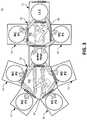
- reaction chamber configuration 90shown in FIG. 2
- a number of reaction chambers 60may be disposed around and/or coupled to a TC 80 comprising a transfer tool 85 for transferring substrates between reaction chambers 60 .
- a number of reaction chambers 61may surround and/or be coupled to one or more TCs (e.g., TCs 81 and 82 ).
- Each TCmay comprise one or more transfer tools (e.g., transfer tool 86 comprised in TC 81 and transfer tool 87 comprised in TC 82 ).
- Such embodiments of reactor systemsmay comprise reaction chambers having one gate configured to allow transfer of a substrate(s) in and out of the respective reaction chamber (e.g., a gate which fluidly couples the respective reaction chamber with a TC and/or an LLC, such as LLC 70 or 71 ).
- the transfer tools in a reactor systemmay be configured to transfer substrates between chambers (e.g., between reaction chambers) to begin or during a processing method.
- a substratemay be transferred between different reaction chambers in a reactor system for different steps within a substrate processing method (e.g., to create a semiconductor).
- a transfer toolmay not be able to keep up with the required substrate transfers in the required time.
- a substrate in a certain reaction chamber of a reactor systemmay be required to remain in a reaction chamber after the process step in such a reaction chamber is complete, before being transferred to another reaction chamber.
- Such waitingmay decrease the efficiency of a reactor system to produce finished products (e.g., semiconductors) and/or may diminish the quality of the finished products.
- a reactor systemmay comprise a plurality of reaction chambers; a plurality of transfer chambers; and/or at least two gate valves coupled to each reaction chamber of the plurality of reaction chambers.
- a first gate valve of the at least two gate valvesmay fluidly couple a first respective reaction chamber of the plurality of reaction chambers to a first transfer chamber of the plurality of transfer chambers, and a second gate valve of the at least two gate valves may fluidly couple the first respective reaction chamber to a second transfer chamber of the plurality of transfer chambers.
- each of the plurality of transfer chambersmay comprise a transfer tool, wherein each transfer tool may be configured to transfer a substrate into and/or out of multiple (e.g., at least two, or a maximum of two) of the plurality of reaction chambers.
- a reactor systemmay comprise a first reaction chamber; a first reaction chamber first gate valve coupled to the first reaction chamber and configured to allow transferring a substrate into and/or out of the first reaction chamber; a first transfer chamber, wherein the first transfer chamber may be in fluid communication with the first reaction chamber via the first reaction chamber first gate valve in response to the first reaction chamber first gate valve being open, wherein the reactor system may be configured to allow transfer of the substrate between the first reaction chamber and the first transfer chamber through the first reaction chamber first gate valve; a first reaction chamber second gate valve coupled to the first reaction chamber and configured to allow transferring a substrate into and/or out of the first reaction chamber; and/or a second transfer chamber in fluid communication with the first reaction chamber via of the first reaction chamber second gate valve in response to the first reaction chamber second gate valve being open, wherein the reactor system may be configured to allow transfer of the substrate between the first reaction chamber and the second transfer chamber through the first reaction chamber second gate valve.
- first transfer chamber and the second transfer chambermay be on opposite sides of the first reaction chamber from one another. In various embodiments, the first transfer chamber and the second transfer chamber may be disposed less than 180 degrees about the first reaction chamber from one another.
- a reactor systemmay further comprise a second reaction chamber; and a second reaction chamber first gate valve coupled to the second reaction chamber and configured to allow transferring the substrate into and/or out of the second reaction chamber.
- the second reaction chambermay be in fluid communication with the second transfer chamber via the second reaction chamber first gate valve in response to the second reaction chamber first gate valve being open.
- a reactor systemmay further comprise a second reaction chamber second gate valve coupled to the second reaction chamber.
- the second reaction chambermay be in fluid communication with the first transfer chamber via the second reaction chamber second gate valve in response to the second reaction chamber second gate valve being open.
- a reactor systemmay further comprise a third transfer chamber; and/or a second reaction chamber second gate valve coupled to the second reaction chamber.
- the second reaction chambermay be in fluid communication with the third transfer chamber via the second reaction chamber second gate valve in response to the second reaction chamber second gate valve being open.
- a reactor systemmay further comprise a third reaction chamber; and/or a third reaction chamber first gate valve coupled to the third reaction chamber and configured to allow transferring the substrate into and/or out of the third reaction chamber.
- the third reaction chambermay be in fluid communication with the third transfer chamber via the third reaction chamber first gate valve in response to the third reaction chamber first gate valve being open.
- a reactor systemmay further comprise a third reaction chamber second gate valve coupled to the third reaction chamber.
- the third reaction chambermay be in fluid communication with at least one of the first transfer chamber or the second transfer chamber via the third reaction chamber second gate valve in response to the third reaction chamber second gate valve being open.
- a reactor systemmay further comprise a fourth transfer chamber; and/or a third reaction chamber third gate valve coupled to the third reaction chamber.
- the third reaction chambermay be in fluid communication with the fourth transfer chamber via the third reaction chamber third gate valve in response to the third reaction chamber third gate valve being open.
- a reactor systemmay further comprise a fourth transfer chamber; and/or a third reaction chamber second gate valve coupled to the third reaction chamber.
- the third reaction chambermay be in fluid communication with the fourth transfer chamber via the third reaction chamber second gate valve in response to the third reaction chamber second gate valve being open.
- a reactor systemmay further comprise a first reaction chamber third gate valve coupled to the first reaction chamber.
- the fourth transfer chambermay be in fluid communication with the first reaction chamber via the first reaction chamber third gate valve in response to the first reaction chamber third gate valve being open.
- a reactor systemmay further comprise a fourth reaction chamber; and/or a fourth reaction chamber first gate valve coupled to the fourth reaction chamber and configured to allow transferring the substrate into and/or out of the fourth reaction chamber.
- the fourth reaction chambermay be in fluid communication with the fourth transfer chamber via the fourth reaction chamber first gate valve in response to the fourth reaction chamber first gate valve being open.
- a reactor systemmay further comprise a fourth reaction chamber second gate valve coupled to the fourth reaction chamber.
- the fourth reaction chambermay be in fluid communication with the first transfer chamber via the fourth reaction chamber second gate valve in response to the fourth reaction chamber second gate valve being open.
- a methodmay comprise transferring a first substrate to a first reaction chamber through a first reaction chamber first gate valve coupled to the first reaction chamber, via a first transfer tool comprised in a first transfer chamber, wherein the first reaction chamber and the first transfer chamber may be in fluid communication in response to the first reaction chamber first gate valve being opened; transferring the first substrate from the first reaction chamber through a first reaction chamber second gate valve coupled to the first reaction chamber, via a second transfer tool comprised in a second transfer chamber, wherein the second transfer chamber may be in fluid communication with the first reaction chamber in response to the first reaction chamber second gate valve being opened; transferring, via the second transfer tool, the substrate to a second reaction chamber through a second reaction chamber first gate valve coupled to the second reaction chamber, wherein the second reaction chamber may be in fluid communication with the second transfer chamber in response to the second reaction chamber first gate valve being opened; and/or transferring the substrate from the second reaction chamber.
- the transferring the substrate from the second reaction chambermay be completed via the first transfer tool through a second reaction chamber second gate valve coupled to the second reaction chamber, wherein the second reaction chamber and the first transfer chamber may be in fluid communication in response to the second reaction chamber second gate valve being opened.
- the methodmay further comprise applying a first material to the substrate in the first reaction chamber for a first duration before the transferring the substrate from the first reaction chamber; and/or applying a second material to the substrate in the second reaction chamber for a second duration before the transferring the substrate from the second reaction chamber.
- the first duration and the second durationmay be the same.
- transferring the substrate from the second reaction chambermay be completed via a third transfer tool comprised in a third transfer chamber and through a second reaction chamber second gate valve coupled to the second reaction chamber, wherein the second reaction chamber and the third transfer chamber may be in fluid communication in response to the second reaction chamber second gate valve being opened.
- the methodmay further comprise applying a first material to the substrate in the first reaction chamber for a first duration before the transferring the substrate from the first reaction chamber; applying a second material to the substrate in the second reaction chamber for a second duration before the transferring the substrate from the second reaction chamber; transferring, via the third transfer tool, the substrate to a third reaction chamber through a third reaction chamber first gate valve coupled to the third reaction chamber, wherein the third reaction chamber is in fluid communication with the third transfer chamber in response to the third reaction chamber first gate valve being opened; and/or applying a third material to the substrate in the third reaction chamber for a third duration.
- the second material and the third materialmay be the same, and the first duration, the second duration, and the third duration may be the same.
- FIG. 1illustrates a schematic diagram of a reactor system, in accordance with various embodiments.
- FIG. 2illustrates a schematic diagram of a reactor system.
- FIG. 3illustrates another schematic diagram of a reactor system.
- FIGS. 4A-Cillustrate schematic diagrams of reactor systems comprising multi-directional reaction chambers, in accordance with various embodiments.
- FIGS. 5A and 5Billustrate schematic diagrams of other reactor systems comprising multi-directional reaction chambers, in accordance with various embodiments.
- substratemay refer to any underlying material or materials that may be used, or upon which, a device, a circuit, or a film may be formed.
- the term “atomic layer deposition”may refer to a vapor deposition process in which deposition cycles, preferably a plurality of consecutive deposition cycles, are conducted in a process chamber.
- the precursormay be chemisorbed to a deposition surface (e.g., a substrate surface or a previously deposited underlying surface such as material from a previous ALD cycle), forming a monolayer or sub-monolayer that does not readily react with additional precursor (i.e., a self-limiting reaction).
- a reactante.g., another precursor or reaction gas
- This reactantmay be capable of further reaction with the precursor.
- purging stepsmay also be utilized during each cycle to remove excess precursor from the process chamber and/or remove excess reactant and/or reaction byproducts from the process chamber after conversion of the chemisorbed precursor.
- atomic layer depositionis also meant to include processes designated by related terms such as, chemical vapor atomic layer deposition, atomic layer epitaxy (ALE), molecular beam epitaxy (MBE), gas source MBE, or organometallic MBE, and chemical beam epitaxy when performed with alternating pulses of precursor composition(s), reactive gas, and purge (e.g., inert carrier) gas.
- CVDchemical vapor deposition
- film and “thin film”may refer to any continuous or non-continuous structures and material deposited by the methods disclosed herein.
- film and “thin film”could include 2D materials, nanorods, nanotubes, or nanoparticles or even partial or full molecular layers or partial or full atomic layers or clusters of atoms and/or molecules.
- Finm and “thin film”may comprise material or a layer with pinholes, but still be at least partially continuous.
- contaminantmay refer to any unwanted material disposed within the reaction chamber that may affect the purity of a substrate or layer disposed in the reaction chamber, or any unwanted material in any component of a reactor system.
- contaminantmay refer to, but is not limited to, unwanted deposits, metal and non-metal particles, impurities, and waste products, disposed within the reaction chamber or other components of the reactor system.
- gasmay include vaporized solid and/or liquid and may be constituted by a single gas or a mixture of gases.
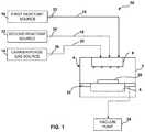
- a reactor system 50may comprise a reaction chamber 4 , a susceptor 6 to hold a substrate 30 during processing, a gas distribution system 8 (e.g., a showerhead) to distribute one or more reactants to a surface of substrate 30 , one or more reactant sources 10 , 12 , and/or a carrier and/or purge gas source 14 , fluidly coupled to reaction chamber 4 via lines 16 - 20 , and valves or controllers 22 - 26 .
- a gas distribution system 8e.g., a showerhead
- Reactant gases or other materials from reactant sources 10 , 12may be applied to substrate 30 in reaction chamber 4 .
- a purge gas from purge gas source 14may be flowed to and through reaction chamber 4 to remove any excess reactant or other undesired materials from reaction chamber 4 .
- System 50may also comprise a vacuum source 28 fluidly coupled to the reaction chamber 4 , which may be configured to suck reactants, a purge gas, and/or other materials out of reaction chamber 4 .
- a substrate processing methodmay comprise multiple steps, which may be performed in multiple reaction chambers. For example, a first precursor may be applied to a substrate in one reaction chamber for a determined duration, the substrate may be transferred to another reaction chamber, and then a second precursor may be applied to the substrate. Additionally or alternatively, a first layer can be deposited in a first reaction chamber and additional reaction chamber(s) can be used for etching, cleaning, and/or for additional deposition processes.
- Timely transfer of a substrate between reaction chambersmay facilitate more efficient substrate processing in a reactor system and/or better resulting final products (e.g., especially for final products made by processing methods having time-sensitive steps and/or involving unstable compounds that may degrade or otherwise react if processing does not continue within a desired timeframe and/or without exposure to an ambient environment).
- a reactor systemmay comprise a plurality of reaction chambers (e.g., each within a respective reactor). Each reactor and/or reaction chamber may have a surrounding wall. The surrounding wall may enclose a reaction chamber space of the reaction chamber in which a substrate may be disposed for processing.
- a reactor systemmay comprise at least two gate valves coupled to each reaction chamber (e.g., coupled to the surrounding wall of each reaction chamber), wherein each gate valve may be configured to selectively allow access to the respective reaction chamber.
- each gate valvemay open to allow transfer of a substrate in and out of the respective reaction chamber (fluidly coupling the respective reaction chamber with another chamber of the reactor system, such as a transfer chamber), and close to at least partially seal the reaction chamber from the surrounding environment.
- the gate valves for gaining access to a respective reaction chambermay be closed during substrate processing in the respective reaction chamber. Because there may be at least two gate valves coupled to each reaction chamber, and each gate valve may allow transfer of a substrate in or out of each reaction chamber to different destinations within the reactor system (e.g., other chambers), such reaction chambers may be multi-directional reaction chambers.
- a reactor systemmay further comprise a plurality of transfer chambers.
- Each transfer chambermay comprise a transfer chamber surrounding wall and a transfer tool (e.g., a transfer arm) disposed therein.
- the transfer toolmay be configured to transfer a substrate(s) in and out of one or more reaction chambers, and/or in or out of the respective transfer chamber.
- a transfer chambermay be coupled to at least two gate valves, which allow fluid communication between other chambers in the reactor system (e.g., allowing substrate transfer therebetween).
- each reaction chamber in the reactor systemmay be coupled and/or adjacent to at least two transfer chambers.
- each transfer chambermay be coupled and/or adjacent to at least two reaction chambers.
- a first of the at least two gate valves coupled to a reaction chambermay fluidly couple the reaction chamber to a first transfer chamber of the plurality of transfer chambers, such that a substrate may be transferred between the first transfer chamber and the reaction chamber in response to the respective gate valve being open.
- a second of the at least two gate valves coupled to the reaction chambermay fluidly couple the reaction chamber to a second transfer chamber of the plurality of transfer chambers, such that a substrate may be transferred between the second transfer chamber and the reaction chamber in response to the respective gate valve being open.
- a reaction chambermay be coupled to any suitable number of gate valves, each of which may couple the reaction chamber to a transfer chamber.
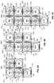
- the arrangement of the reaction chambers and transfer chambers in a reactor systemmay be in any suitable configuration such that each reaction chamber may be coupled to at least two gate valves, each of which fluidly couples the reaction chamber with a transfer chamber (so the reaction chamber is fluidly coupled to at least two transfer chambers, one for each gate valve), and such that each transfer chamber is coupled and/or adjacent to two or more chambers (e.g., two or three chambers, which can comprise a reaction chamber, a load lock chamber, a buffer chamber, and/or any other space from or into which a substrate may be transferred by a transfer tool in a transfer chamber). Examples of such reactor system configurations of reaction chambers and transfer chambers are illustrated in FIGS. 4A-4C, 5A and 5B , discussed further herein.
- each transfer chambermay have a reduced number of possible substrate transfers (e.g., two or three), such that substrate “traffic jams” will be minimized or prevented (rather than transfer chambers having six or more possible substrate transfers, such as the in the reactor systems depicted in FIGS. 2 and 3 ).
- each transfer chamber in the reactor systemmay be adjacent and/or coupled to a maximum of two or three chambers (e.g., reaction chambers, load lock chambers, buffer chambers, and/or the like). Accordingly, in such embodiments, each transfer chamber and/or the transfer tool(s) comprised therein may have a maximum of two or three possible substrate transfers to perform between chambers.
- a reactor systemmay comprise a first reaction chamber (e.g., first reaction chamber 110 ).
- First reaction chamber 110may comprise a first surrounding wall 112 .
- the surrounding wall of a reaction chambermay comprise any suitable design or shape.
- a surrounding wall of a reaction chambermay comprise a number of surrounding wall sides (e.g., three, four, six, or eight sides), wherein one or more of the surrounding wall sides is coupled to a gate valve.
- a gate valvemay be configured to open and close, exposing or at least partially sealing, respectively, the reaction chamber space of first reaction chamber 110 .
- the reaction chamber coupled to the gate valvemay be in fluid communication with another chamber in the reactor system.
- first reaction chamber 110may be coupled to a first reaction chamber first gate valve 114 .
- First reaction chamber first gate valve 114may allow the transfer of a substrate in and out of first reaction chamber 110 .
- reactor system 400 Amay comprise a first transfer chamber 210 having a first transfer chamber surrounding wall 212 .
- First transfer chamber 210may be disposed adjacent to, and/or coupled to, first reaction chamber 110 and/or first reaction chamber first gate valve 114 .
- First reaction chamber first gate valve 114may cause first reaction chamber 110 and first transfer chamber 210 to be in fluid communication (e.g., in response to first reaction chamber first gate valve 114 being open).
- a first transfer tool 213 comprised in first transfer chamber 210may be able to transfer one or more substrates in and out of first reaction chamber 110 through first reaction chamber first gate valve 114 .
- Another chamber of the reactor systemmay be adjacent and/or coupled to first transfer chamber 210 , from which first transfer tool 213 may receive substrates to be transferred to first reaction chamber 110 and/or to which first transfer tool 213 may transfer substrates from first reaction chamber 110 and/or another chamber in reactor system 400 A.
- a load lock chamber (LLC) 105may be coupled and/or adjacent to first transfer chamber 210 . LLC 105 may be configured to hold substrates awaiting processing and/or substrates which have been processed. Therefore, first transfer chamber 210 may transfer substrates awaiting processing from LLC 105 to first reaction chamber 110 and/or transfer finished products (e.g., processed substrates) from a final reaction chamber used in the process to LLC 105 .
- the final reaction chamber in a reactor systemmay be the last reaction chamber used in a process, or the reaction chamber from which substrates may be loaded into an LLC by a transfer chamber after processing.
- the first transfer chamber in a reactor systemin the embodiments disclosed herein, may be the transfer chamber configured to retrieve and/or deliver substrates to and from the LLC.
- the first transfer chamber and the LLCmay be coupled to an LLC gate valve (e.g., LLC gate valve 107 ), through which a substrate(s) may be transferred between the first transfer chamber and the LLC.
- LLC gate valvee.g., LLC gate valve 107
- reactor system 400 Amay comprise a second transfer chamber 220 A having a second transfer chamber surrounding wall 222 A.
- Second transfer chamber 220 Amay be coupled and/or adjacent to first reaction chamber 110 .
- Reactor system 400 Amay further comprise a first reaction chamber second gate valve 116 A coupled to first reaction chamber 110 and/or second transfer chamber 220 A.
- Second transfer chamber 220 Amay be coupled and/or disposed adjacent to first reaction chamber 110 and/or first reaction chamber second gate valve 116 A.
- First reaction chamber second gate valve 116 Amay cause first reaction chamber 110 and second transfer chamber 220 A to be in fluid communication (e.g., in response to first reaction chamber second gate valve 116 A being open).
- a second transfer tool 223 A comprised in second transfer chamber 220 Amay be able to transfer one or more substrates in and out of first reaction chamber 110 through first reaction chamber second gate valve 116 A.
- First transfer chamber 210 and second transfer chamber 220 Amay be coupled to first reaction chamber 110 in any suitable configuration relative to one another.
- first transfer chamber 210 and second transfer chamber 220 Amay be disposed on opposite sides of first reaction chamber 110 from one another.
- first transfer chamber 210 and second transfer chamber 220 Amay be disposed 180 degrees from one another with first reaction chamber 110 therebetween.
- first transfer chamber 210 and second transfer chamber 220 Amay be disposed less than 180 degrees from one another (e.g., about 90 degrees, about 120 degrees, or about 60 degrees from one another). In this context, “about” means plus or minus 20 or 30 degrees.
- first transfer chamber 210 and second transfer chamber 220 Amay be disposed 90 degrees from one another.
- a reactor systemmay comprise a second reaction chamber (e.g., second reaction chamber 120 A).
- Second reaction chamber 120 Amay comprise a second surrounding wall 122 A.
- Second reaction chamber 120 Amay be adjacent and/or coupled to second transfer chamber 220 A.
- Reactor system 400 Amay comprise a second reaction chamber first gate valve 124 A coupled to second reaction chamber 120 A and/or second transfer chamber 220 A.
- Second reaction chamber first gate valve 124 Ain response to being open, may fluidly couple second transfer chamber 220 A and second reaction chamber 120 A, such that transfer of a substrate in and out of second reaction chamber 120 A may occur through second reaction chamber first gate valve 124 A. Such substrate transfer may be accomplished by second transfer tool 223 A.
- reactor system 400 Amay further comprise a second reaction chamber second gate valve 126 A.
- Second reaction chamber second gate valve 126 Amay be coupled to second reaction chamber 120 A and/or first transfer chamber 210 .
- Second reaction chamber second gate valve 126 Ain response to being open, may fluidly couple second reaction chamber 120 A and first transfer chamber 210 , such that transfer of a substrate in and out of second reaction chamber 120 A may occur through second reaction chamber second gate valve 126 A.
- Such substrate transfermay be accomplished by first transfer tool 213 .
- Second reaction chamber 120 A and first transfer chamber 210may be adjacent and/or coupled.
- second reaction chamber 120 Amay be the final reaction chamber, from which substrates are transferred to LLC 105 after processing.
- a reactor systeme.g., reactor system 400 A
- the LLCmay be coupled to a transfer chamber in any suitable position.
- the LLCmay be positioned closer to one reaction chamber in the reactor system than another reaction chamber.
- LLC 105is positioned on an opposite side of first transfer chamber 210 than first reaction chamber 110 (and thus, closer to second reaction chamber 120 A), but in various embodiments, for example, LLC 105 may be positioned on an opposite side of first transfer chamber 210 than second reaction chamber 120 A (and thus, closer to first reaction chamber 110 ).
- the reaction chambers in reactor system 400 Aeach have at least two gate valves coupled thereto, and therefore, are multi-directional reaction chambers because there are more than one entrance/exit for a substrate to be transferred in and out of each reaction chamber.
- a substratemay be transferred from LLC 105 to first reaction chamber 110 through first transfer chamber 210 via first transfer tool 213 .
- First transfer tool 213may obtain the substrate from LLC 105 through LLC gate valve 107 (in response to LLC gate valve 107 being open), and transfer the substrate to first transfer chamber 210 .
- LLC gate valve 107may close and/or first reaction chamber first gate valve 114 may open.
- First transfer tool 213may deliver the substrate to first reaction chamber 110 through first reaction chamber first gate valve 114 (in response to first reaction chamber first gate valve 114 being open).
- first reaction chamber first gate valve 114may close to at least partially seal first reaction chamber 110 so one or more processing steps may occur (e.g., application of one or more gases (such as reactant gases and/or purge gases) to the substrate in first reaction chamber 110 ).
- first reaction chamber second gate valve 116 Amay also be closed to at least partially seal first reaction chamber 110 .
- first reaction chamber second gate valve 116 Amay open and second transfer tool 223 A may obtain the substrate from first reaction chamber 110 and transfer the substrate to second transfer chamber 220 A.
- first reaction chamber second gate valve 116 Amay close and/or second reaction chamber first gate valve 124 A may open.
- Second transfer tool 223 Amay deliver the substrate to second reaction chamber 120 A through second reaction chamber first gate valve 124 A (in response to second reaction chamber first gate valve 124 A being open).
- second reaction chamber first gate valve 124 Amay close to at least partially seal second reaction chamber 120 A so one or more processing steps may occur to the substrate in second reaction chamber 120 A.
- second reaction chamber second gate valve 126 Amay also be closed to at least partially seal second reaction chamber 120 A.
- second reaction chamber second gate valve 126 Amay open and first transfer tool 213 may obtain the substrate from second reaction chamber 120 A and transfer the substrate to first transfer chamber 210 (or to first reaction chamber 110 again for further processing).
- An LLCmay be coupled to another gate valve (e.g., gate valve 108 ), which may be configured to allow loading of substrates for processing into the LLC (e.g., by an operator of the reactor system) or unloaded processed substrates from the LLC.
- first reaction chamber 110 and/or second reaction chamber 120 Amay comprise the same or different processing of the substrate. That is, a first process may occur in first reaction chamber 110 and a second process may occur in second reaction chamber 120 A, for any suitable duration, with any suitable number of steps.
- a processmay comprise two steps (e.g., applying a first material to the substrate and then applying a second material to the substrate), wherein one step is performed in first reaction chamber 110 and the other is performed in second reaction chamber 120 A.
- a processmay comprise one step, which may comprise a processing duration.
- the entire processing durationmay be performed in either first reaction chamber 110 or second reaction chamber 120 A, or processing for one-half of the duration may occur in first reaction chamber 110 and processing for the other half of the duration may occur in second reaction chamber 120 A.
- the substratemay travel between the chambers in a reactor system in any suitable order (e.g., an order that is the reverse of that described herein).
- a reactor system 400 Bmay comprise LLC 105 , LLC gate valve 107 , first transfer chamber 210 , first reaction chamber 110 , and first reaction chamber first gate valve 114 , and any components therein, similar to reactor system 400 A of FIG. 4A , discussed herein.
- reactor system 400 Bmay comprise a second transfer chamber 220 B coupled and/or adjacent to first reaction chamber 110 . Unlike second transfer chamber 220 A in reactor system 400 A, second transfer chamber 220 B may be on an opposite side of first reaction chamber 110 than first transfer chamber 210 .
- Reactor system 400 Bmay comprise a first reaction chamber second gate valve 116 B coupled to first reaction chamber 110 and/or second transfer chamber 220 B.
- First reaction chamber second gate valve 116 Bmay cause first reaction chamber 110 and second transfer chamber 220 B to be in fluid communication (e.g., in response to first reaction chamber second gate valve 116 B being open).
- a second transfer tool 223 B comprised in second transfer chamber 220 Bmay be able to transfer one or more substrates in and out of first reaction chamber 110 through first reaction chamber second gate valve 116 B.
- a reactor systemmay comprise a second reaction chamber (e.g., second reaction chamber 120 B).
- Second reaction chamber 120 Bmay comprise a second surrounding wall 122 B.
- Second reaction chamber 120 Bmay be adjacent and/or coupled to second transfer chamber 220 A.
- Reactor system 400 Bmay comprise a second reaction chamber first gate valve 124 B coupled to second reaction chamber 120 B and/or to second transfer chamber 220 B.
- Second reaction chamber first gate valve 124 Bin response to being open, may fluidly couple second transfer chamber 220 B and second reaction chamber 120 B, such that transfer of a substrate in and out of second reaction chamber 120 B may occur through second reaction chamber first gate valve 124 B. Such substrate transfer may be accomplished by second transfer tool 223 B.
- reactor system 400 Bmay comprise a third transfer chamber (e.g., third transfer chamber 230 B).
- Third transfer chamber 230 Bmay comprise a third surrounding wall 232 B.
- Third transfer chamber 230 Bmay be adjacent and/or coupled to second reaction chamber 120 B.
- Third transfer chamber 230 Bmay comprise a third transfer tool 233 B configured to transfer substrates in and out of third transfer chamber 230 B.
- reactor system 400 Bmay further comprise a second reaction chamber second gate valve 126 B.
- Second reaction chamber second gate valve 126 Bmay be coupled to second reaction chamber 120 B and/or third transfer chamber 230 B.
- Second reaction chamber second gate valve 126 Bin response to being open, may fluidly couple second reaction chamber 120 B and third transfer chamber 230 B, such that transfer of a substrate in and out of second reaction chamber 120 B may occur through second reaction chamber second gate valve 126 B.
- Such substrate transfermay be accomplished by third transfer tool 233 B.
- a reactor systemmay comprise a third reaction chamber (e.g., third reaction chamber 130 B).
- Third reaction chamber 130 Bmay comprise a third surrounding wall 132 B.
- Third reaction chamber 130 Bmay be adjacent and/or coupled to third transfer chamber 230 B.
- Reactor system 400 Bmay comprise a third reaction chamber first gate valve 134 B coupled to third reaction chamber 130 B and/or third transfer chamber 230 B.
- Third reaction chamber first gate valve 134 Bin response to being open, may fluidly couple third transfer chamber 230 B and third reaction chamber 130 B, such that transfer of a substrate in and out of third reaction chamber 130 B may occur through third reaction chamber first gate valve 134 B. Such substrate transfer may be accomplished by third transfer tool 233 B.
- reactor system 400 Bmay further comprise a third reaction chamber second gate valve 136 B.
- Third reaction chamber second gate valve 136 Bmay be coupled to third reaction chamber 130 B and/or first transfer chamber 210 .
- Third reaction chamber second gate valve 136 Bin response to being open, may fluidly couple third reaction chamber 130 B and first transfer chamber 210 , such that transfer of a substrate in and out of third reaction chamber 130 B may occur through third reaction chamber second gate valve 136 B.
- Such substrate transfermay be accomplished by first transfer tool 213 .
- Third reaction chamber 130 B and first transfer chamber 210may be adjacent and/or coupled.
- third reaction chamber 130 Bmay be the final reaction chamber, from which substrates are transferred to LLC 105 after processing.
- a reactor systeme.g., reactor system 400 B
- the LLCmay be coupled to a transfer chamber in any suitable position. For example, the LLC may be positioned closer to one reaction chamber in the reactor system than another reaction chamber.
- LLC 105is positioned on an opposite side of first transfer chamber 210 than first reaction chamber 110 (and thus, closer to third reaction chamber 130 B), but in various embodiments, for example, LLC 105 may be positioned on an opposite side of first transfer chamber 210 than third reaction chamber 130 B (and thus, closer to first reaction chamber 110 ).
- the reaction chambers in reactor system 400 Beach have at least two gate valves coupled thereto, and therefore, are multi-directional reaction chambers because there are more than one entrance/exit for a substrate to be transferred in and out of each reaction chamber.
- a substratemay be transferred from LLC 105 to first reaction chamber 110 through first transfer chamber 210 and via first transfer tool 213 .
- First transfer tool 213may obtain the substrate from LLC 105 through LLC gate valve 107 (in response to LLC gate valve 107 being open), and transfer the substrate to first transfer chamber 210 .
- LLC gate valve 107may close and/or first reaction chamber first gate valve 114 may open.
- First transfer tool 213may deliver the substrate to first reaction chamber 110 through first reaction chamber first gate valve 114 (in response to first reaction chamber first gate valve 114 being open).
- first reaction chamber first gate valve 114may close to at least partially seal first reaction chamber 110 so one or more processing steps may occur (e.g., application of one or more gases (such as reactant gases and/or purge gases) to the substrate in first reaction chamber 110 ).
- first reaction chamber second gate valve 116 Bmay also be closed to at least partially seal first reaction chamber 110 .
- first reaction chamber second gate valve 116 Bmay open and second transfer tool 223 B may obtain the substrate from first reaction chamber 110 and transfer the substrate to second transfer chamber 220 B.
- first reaction chamber second gate valve 116 Bmay close and/or second reaction chamber first gate valve 124 B may open.
- Second transfer tool 223 Bmay deliver the substrate to second reaction chamber 120 B through second reaction chamber first gate valve 124 B (in response to second reaction chamber first gate valve 124 B being open).
- second reaction chamber first gate valve 124 Bmay close to at least partially seal second reaction chamber 120 B so one or more processing steps may occur to the substrate in second reaction chamber 120 B.
- second reaction chamber second gate valve 126 Bmay also be closed to at least partially seal second reaction chamber 120 B.
- second reaction chamber second gate valve 126 Bmay open and third transfer tool 233 B may obtain the substrate from second reaction chamber 120 B and transfer the substrate to third transfer chamber 230 B.
- second reaction chamber second gate valve 126 Bmay close and/or third reaction chamber first gate valve 134 B may open.
- Third transfer tool 233 Bmay deliver the substrate to third reaction chamber 130 B through third reaction chamber first gate valve 134 B (in response to third reaction chamber first gate valve 134 B being open).
- third reaction chamber first gate valve 134 Bmay close to at least partially seal third reaction chamber 130 B so one or more processing steps may occur to the substrate in third reaction chamber 130 B.
- third reaction chamber second gate valve 136 Bmay also be closed to at least partially seal third reaction chamber 130 B.
- third reaction chamber second gate valve 136 Bmay open and first transfer tool 213 may obtain the substrate from third reaction chamber 130 B and transfer the substrate to first transfer chamber 210 (or to first reaction chamber 110 again for further processing).
- first reaction chamber 110second reaction chamber 120 B, and/or third reaction chamber 130 B may comprise the same or different processing of the substrate. That is, a first process may occur in first reaction chamber 110 , a second process may occur in second reaction chamber 120 B, and/or a third process may occur in third reaction chamber 130 B, for any suitable duration, with any suitable number of steps.
- a processmay comprise three steps, wherein one step is performed in first reaction chamber 110 , one step is performed in second reaction chamber 120 B, and the final step is performed in third reaction chamber 130 B (e.g., with each step having equal or different durations).
- processing a substratemay comprise one step (e.g., applying a first material to the substrate for a first duration) and a second step (e.g., applying a second material to the substrate for a second duration).
- the second durationmay be longer (e.g., twice as long) as the first duration.
- the first stepmay be performed in first reaction chamber 110
- the second stepmay be split between second reaction chamber 120 B and third reaction chamber 130 B (e.g., a second material being applied to the substrate in second reaction chamber 120 B for half of the second duration (which may be equal to the first duration), and a third material being applied to the substrate in third reaction chamber 130 B for the other half of the second duration (which may be the same as the second material to complete the second step of the process).
- the process stepsmay be spread out between the reaction chambers such that the substrates continually advance through the chambers of the reactor system such that substrate transfer delays between chambers (i.e., a substrate that has finished a process step in a reaction chamber waiting in the reaction chamber or the next transfer chamber to enter the subsequent reaction chamber) are minimized or prevented.
- a processmay comprise one step, which may comprise a processing duration.
- the entire processing durationmay be performed in either first reaction chamber 110 , second reaction chamber 120 B, and/or third reaction chamber 130 B, or processing for one-third of the duration may occur in first reaction chamber 110 , processing for a second one-third of the duration may occur in second reaction chamber 120 B, and processing for the final one-third of the duration may occur in third reaction chamber 130 B (or any other division of processing and/or processing duration between at least some of the reaction chambers).
- the substratemay travel between the chambers in a reactor system in any suitable order (e.g., an order that is the reverse of that described herein).
- a reactor system 400 Cmay comprise LLC 105 , LLC gate valve 107 , first transfer chamber 210 , first reaction chamber 110 , and first reaction chamber first gate valve 114 , and any components therein, similar to reactor systems 400 A and 400 B, discussed herein. Additionally, reactor system 400 C may comprise first reaction chamber second gate valve 116 B and second transfer chamber 220 B, and any components therein, similar to reactor system 400 B. In various embodiments, reactor system 400 C may comprise a second transfer chamber 220 B coupled and/or adjacent to first reaction chamber 110 . Reactor system 400 C may comprise a first reaction chamber second gate valve 116 B coupled to first reaction chamber 110 and/or second transfer chamber 220 B.
- First reaction chamber second gate valve 116 Bmay cause first reaction chamber 110 and second transfer chamber 220 B to be in fluid communication (e.g., in response to first reaction chamber second gate valve 116 B being open).
- a second transfer tool 223 B comprised in second transfer chamber 220 Bmay be able to transfer one or more substrates in and out of first reaction chamber 110 through first reaction chamber second gate valve 116 B.
- a reactor systemmay comprise a second reaction chamber (e.g., second reaction chamber 120 C).
- Second reaction chamber 120 Cmay comprise a second surrounding wall 122 C.
- Second reaction chamber 120 Cmay be coupled to second transfer chamber 220 B.
- Second reaction chamber 120 Cmay be positioned opposite from 110 , with second transfer chamber 220 B therebetween between.
- the chambersmay be positioned in any suitable arrangement, so second reaction chamber 120 C may be positioned relative first reaction chamber 110 with second transfer chamber 220 B therebetween in any suitable manner.
- Reactor system 400 Cmay comprise a second reaction chamber first gate valve 124 C coupled to second reaction chamber 120 C and/or second transfer chamber 220 B.
- Second reaction chamber first gate valve 124 Cin response to being open, may fluidly couple second transfer chamber 220 B and second reaction chamber 120 C, such that transfer of a substrate in and out of second reaction chamber 120 C may occur through second reaction chamber first gate valve 124 C. Such substrate transfer may be accomplished by second transfer tool 223 B.
- reactor system 400 Cmay comprise a third transfer chamber (e.g., third transfer chamber 230 C).
- Third transfer chamber 230 Cmay comprise a third surrounding wall 232 C.
- Third transfer chamber 230 Cmay be adjacent and/or coupled to second reaction chamber 120 C.
- Third transfer chamber 230 Cmay comprise a third transfer tool 233 C configured to transfer substrates in and out of second reaction chamber 120 C.
- 400 Cmay further comprise a second reaction chamber second gate valve 126 C.
- Second reaction chamber second gate valve 126 Cmay be coupled to second reaction chamber 120 C and/or third transfer chamber 230 C.
- Second reaction chamber second gate valve 126 Cin response to being open, may fluidly couple second reaction chamber 120 C and third transfer chamber 230 C, such that transfer of a substrate in and out of second reaction chamber 120 C may occur through second reaction chamber second gate valve 126 C.
- Such substrate transfermay be accomplished by third transfer tool 233 C.
- a reactor systemmay comprise a third reaction chamber (e.g., third reaction chamber 130 C).
- Third reaction chamber 130 Cmay comprise a third surrounding wall 132 C.
- Third reaction chamber 130 Cmay be adjacent and/or coupled to third transfer chamber 230 C.
- third reaction chamber 130 Cmay be adjacent and/or coupled to second transfer chamber 230 B.
- Reactor system 400 BCmay comprise a third reaction chamber first gate valve 134 C, which may be coupled to third reaction chamber 130 C and/or third transfer chamber 230 C.
- Third reaction chamber first gate valve 134 Cin response to being open, may fluidly couple third transfer chamber 230 C and third reaction chamber 130 C, such that transfer of a substrate in and out of third reaction chamber 130 C may occur through third reaction chamber first gate valve 134 C. Such substrate transfer may be accomplished by third transfer tool 233 C.
- reactor system 400 Cmay comprise a fourth transfer chamber (e.g., fourth transfer chamber 240 C).
- Fourth transfer chamber 240 Cmay comprise a fourth surrounding wall 242 C.
- Fourth transfer chamber 240 Cmay be adjacent and/or coupled to third reaction chamber 130 C.
- fourth transfer chamber 240 Cmay be adjacent and/or coupled to first reaction chamber 110 .
- Fourth transfer chamber 240 Cmay comprise a fourth transfer tool 243 C configured to transfer substrates in and out of third reaction chamber 130 C.
- 400 Cmay further comprise a third reaction chamber second gate valve 136 C.
- Third reaction chamber second gate valve 136 Cmay be coupled to third reaction chamber 130 C and/or fourth transfer chamber 240 C.
- Third reaction chamber second gate valve 136 Cin response to being open, may fluidly couple third reaction chamber 130 C and fourth transfer chamber 240 C, such that transfer of a substrate in and out of third reaction chamber 130 C may occur through third reaction chamber second gate valve 136 C. Such substrate transfer may be accomplished by fourth transfer tool 243 C.
- a reactor systemmay comprise a fourth reaction chamber (e.g., fourth reaction chamber 140 C).
- Fourth reaction chamber 140 Cmay comprise a third surrounding wall 142 C.
- Fourth reaction chamber 140 Cmay be adjacent and/or coupled to fourth transfer chamber 240 C.
- fourth reaction chamber 140 Cmay be adjacent and/or coupled to first transfer chamber 210 .
- reactor system 400 Cmay comprise a fourth reaction chamber first gate valve 144 C, which may be coupled to fourth reaction chamber 140 C and/or fourth transfer chamber 240 C.
- Fourth reaction chamber first gate valve 144 Cin response to being open, may fluidly couple fourth reaction chamber 140 C and fourth transfer chamber 240 C, such that transfer of a substrate in and out of fourth reaction chamber 140 C may occur through fourth reaction chamber first gate valve 144 C.
- Such substrate transfermay be accomplished by fourth transfer tool 243 C.
- reactor system 400 Cmay further comprise a fourth reaction chamber second gate valve 146 C.
- Fourth reaction chamber second gate valve 146 Cmay be coupled to fourth reaction chamber 140 C and/or first transfer chamber 210 .
- Fourth reaction chamber second gate valve 146 Cin response to being open, may fluidly couple fourth reaction chamber 140 C and first transfer chamber 210 , such that transfer of a substrate in and out of fourth reaction chamber 140 C may occur through fourth reaction chamber second gate valve 146 C. Such substrate transfer may be accomplished by first transfer tool 213 .
- Fourth reaction chamber 140 C and first transfer chamber 210may be adjacent and/or coupled.
- fourth reaction chamber 140 Cmay be the final reaction chamber, from which substrates are transferred to LLC 105 after processing.
- a reactor systeme.g., reactor system 400 C
- the LLCmay be coupled to a transfer chamber in any suitable position.
- the LLCmay be positioned closer to one reaction chamber in the reactor system than another reaction chamber.
- LLC 105is positioned on an opposite side of first transfer chamber 210 than first reaction chamber 110 (and thus, closer to fourth reaction chamber 140 C), but in various embodiments, for example, LLC 105 may be positioned on an opposite side of first transfer chamber 210 than fourth reaction chamber 140 C (and thus, closer to first reaction chamber 110 ), similar to the chamber arrangement in reactor system 500 B of FIG. 5B .
- the reaction chambers in reactor system 400 Ceach have at least two gate valves coupled thereto, and therefore, are multi-directional reaction chambers because there are more than one entrance/exit for a substrate to be transferred in and out of each reaction chamber.
- a substratemay be transferred from LLC 105 to first reaction chamber 110 through first transfer chamber 210 and via first transfer tool 213 .
- First transfer tool 213may obtain the substrate from LLC 105 through LLC gate valve 107 (in response to LLC gate valve 107 being open), and transfer the substrate to first transfer chamber 210 .
- LLC gate valve 107may close and/or first reaction chamber first gate valve 114 may open.
- First transfer tool 213may deliver the substrate to first reaction chamber 110 through first reaction chamber first gate valve 114 (in response to first reaction chamber first gate valve 114 being open).
- first reaction chamber first gate valve 114may close to at least partially seal first reaction chamber 110 so one or more processing steps may occur (e.g., application of one or more gases (such as reactant gases and/or purge gases) to the substrate in first reaction chamber 110 ).
- first reaction chamber second gate valve 116 Bmay also be closed to at least partially seal first reaction chamber 110 .
- first reaction chamber second gate valve 116 Bmay open and second transfer tool 223 B may obtain the substrate from first reaction chamber 110 and transfer the substrate to second transfer chamber 220 B.
- first reaction chamber second gate valve 116 Bmay close and/or second reaction chamber first gate valve 124 C may open.
- Second transfer tool 223 Bmay deliver the substrate to second reaction chamber 120 C through second reaction chamber first gate valve 124 C (in response to second reaction chamber first gate valve 124 C being open).
- second reaction chamber first gate valve 124 Cmay close to at least partially seal second reaction chamber 120 C so one or more processing steps may occur to the substrate in second reaction chamber 120 C.
- second reaction chamber second gate valve 126 Cmay also be closed to at least partially seal second reaction chamber 120 C.
- second reaction chamber second gate valve 126 Cmay open and third transfer tool 233 C may obtain the substrate from second reaction chamber 120 C and transfer the substrate to third transfer chamber 230 C.
- second reaction chamber second gate valve 126 Cmay close and/or third reaction chamber first gate valve 134 C may open.
- Third transfer tool 233 Cmay deliver the substrate to third reaction chamber 130 C through third reaction chamber first gate valve 134 C (in response to third reaction chamber first gate valve 134 C being open).
- third reaction chamber first gate valve 134 Cmay close to at least partially seal third reaction chamber 130 C so one or more processing steps may occur to the substrate in third reaction chamber 130 C.
- third reaction chamber second gate valve 136 Cmay also be closed to at least partially seal third reaction chamber 130 C.
- fourth transfer tool 243 Cmay obtain the substrate from third reaction chamber 130 C and transfer the substrate to fourth transfer chamber 240 C. After the substrate enters and/or is disposed in fourth transfer chamber 240 C from third reaction chamber 130 C, third reaction chamber second gate valve 136 C may close and/or fourth reaction chamber first gate valve 144 C may open. Fourth transfer tool 243 C may deliver the substrate to fourth reaction chamber 140 C through fourth reaction chamber first gate valve 144 C (in response to fourth reaction chamber first gate valve 144 C being open).
- fourth reaction chamber first gate valve 144 Cmay close to at least partially seal fourth reaction chamber 140 C so one or more processing steps may occur to the substrate in fourth reaction chamber 140 C.
- fourth reaction chamber second gate valve 146 Cmay also be closed to at least partially seal fourth reaction chamber 140 C.
- fourth reaction chamber second gate valve 146 Cmay open and first transfer tool 213 may obtain the substrate from fourth reaction chamber 140 C and transfer the substrate to first transfer chamber 210 (or to first reaction chamber 110 again for further processing).
- first reaction chamber 110second reaction chamber 120 C, third reaction chamber 130 C, and/or fourth reaction chamber 140 C may comprise the same or different processing of the substrate. That is, a first process may occur in first reaction chamber 110 , a second process may occur in second reaction chamber 120 C, a third process may occur in third reaction chamber 130 C, and/or a fourth process may occur in fourth reaction chamber 140 C for any suitable duration, with any suitable number of steps.
- a processmay comprise four steps, wherein one step is performed in first reaction chamber 110 , one step is performed in second reaction chamber 120 C, another step is performed in third reaction chamber 130 C, and a final step is performed in fourth reaction chamber 140 C (e.g., with each step having equal or different durations).
- processing a substratemay comprise one step (e.g., applying a first material to the substrate for a first duration) and a second step (e.g., applying a second material to the substrate for a second duration).
- the second durationmay be longer (e.g., three times as long) as the first duration.
- the first stepmay be performed in first reaction chamber 110
- the second stepmay be split between second reaction chamber 120 C, third reaction chamber 130 C, and fourth reaction chamber 140 C (e.g., a second material being applied to the substrate in second reaction chamber 120 C for one-third of the second duration (one-third of the second duration may be equal to the first duration), a third material being applied to the substrate in third reaction chamber 130 C for another third of the second duration, and a fourth material being applied to the substrate in fourth reaction chamber 140 C for the final third of the second duration (the first, second, and third materials all may be the same material to complete the second step of the process).
- a second materialbeing applied to the substrate in second reaction chamber 120 C for one-third of the second duration (one-third of the second duration may be equal to the first duration)
- a third materialbeing applied to the substrate in third reaction chamber 130 C for another third of the second duration
- a fourth materialbeing applied to the substrate in fourth reaction chamber 140 C for the final third of the second duration (the first, second, and third materials all
- the process stepsmay be spread out between the reaction chambers such that the substrates continually advance through the chambers of the reactor system such that substrate transfer delays between chambers (i.e., a substrate that has finished a process step in a reaction chamber waiting in the reaction chamber or the next transfer chamber to enter the subsequent reaction chamber) are mitigated or prevented.
- a processmay comprise one step, which may comprise a processing duration.
- the entire processing durationmay be performed in either first reaction chamber 110 , second reaction chamber 120 C, third reaction chamber 130 C, and/or fourth reaction chamber 140 C, or processing for one-fourth of the duration may occur in each of first reaction chamber 110 , second reaction chamber 120 C, third reaction chamber 130 C, and/or fourth reaction chamber 140 C (or any other division of processing and/or processing duration between at least some of the reaction chambers).
- a processmay comprise two steps: a first step having a first duration and the second step having a second duration.
- the first stepmay be performed in first reaction chamber 110 for half of the first duration and in second reaction chamber 120 C for the second half of the first duration
- the second stepmay be performed in third reaction chamber 130 C for half of the second duration and in fourth reaction chamber 140 C for the second half of the second duration.
- FIGS. 4A-4C and 5A and 5Bare for illustrative purposes only, and that substrates may be transferred between chambers in a reaction chamber in any suitable manner or order.
- designation of “first,” “second,” “third,” etc. of chambers, gate valves, etc. within reactor systemdo not necessarily indicate an order through in which a substrate may be transferred, or a chamber or gate valve order or arrangement (i.e., which chambers and/or gate valves may be proximate or adjacent to one another).
- a reactor systemmay comprise additional gate valves coupled between chambers other than those discussed in relation to reactor systems 400 A, 400 B, and 400 C.
- first reaction chamber 110 and/or third transfer chamber 230 Bwhich may be a first reaction chamber third gate valve
- third transfer tool 233 Bmay transfer a substrate in or out of first reaction chamber 110 (e.g., to bypass second reaction chamber 120 B or third reaction chamber 130 B).
- a gate valve(which may be a first reaction chamber third gate valve) coupling first reaction chamber 110 and fourth transfer chamber 240 C (and/or first reaction chamber 110 and fourth transfer chamber 240 C may be coupled), such that fourth transfer tool 243 C may transfer a substrate in or out of first reaction chamber 110 (e.g., to transfer a substrate between first reaction chamber 110 and fourth transfer chamber 240 C (e.g., to bypass second reaction chamber 120 C and/or third reaction chamber 130 C), and/or to transfer a substrate between first reaction chamber 110 and third reaction chamber 130 C (e.g., to bypass second reaction chamber 120 C and/or fourth reaction chamber 140 C)).
- a gate valvewhich may be a first reaction chamber third gate valve
- a gate valve(which may be a second reaction chamber third gate valve) coupling second transfer chamber 220 B and third reaction chamber 130 C (and/or second transfer chamber 220 B and third reaction chamber 130 C may be coupled), such that second transfer tool 223 B may transfer a substrate in or out of third reaction chamber 130 C (e.g., to transfer a substrate between first reaction chamber 110 and third reaction chamber 130 C (e.g., to bypass second reaction chamber 120 C)).
- a chamber in a reactor systemmay have three gate valves coupled thereto to provide additional substrate path options through the chambers of a reactor system (for example, to utilize less than all chambers in a reactor system for a process).
- gate valvesmay be coupled to reaction chambers and/or transfer chambers within a reactor system, and/or coupled to the surrounding walls of the reaction chambers and/or transfer chambers (or any other chambers in the reactor system).
- gate valvesmay be discrete components of a reactor system, or gate valves may be comprised in the reaction chambers and/or transfer chambers (or any other chambers in the reactor system), and/or the surrounding walls thereof.
- each reaction chambermay be comprised in a reactor (e.g., the first reaction chamber may be comprised in a first reactor, the second reaction chamber may be comprised in a second reactor, etc.).
- each reactormay further comprise at least two gate valves coupled to the reaction chamber, and/or at least two gate valves may be coupled to the reactor, the gate valves being configured to selectively allow access to the reaction chamber.
- the gate valves coupled to a chamber or its surrounding wallmay be disposed around such a chamber at any suitable angle(s) relative to other gate valves, such as those angles discussed herein in regard to chambers being disposed relative to one another.
- the arrangement of chambers in a reactor systemmay be in any suitable configuration and/or shape.
- the reaction chambers and transfer chambers of reactor system 400 Amay be arranged so that there is a space between the chambers.
- the reaction chambers and transfer chambers of reactor system 400 Bmay be arranged so that there is a space between the chambers (e.g., which may be accomplished by having reaction chambers positioned at an angle between 90 and 180 relative to other reaction chambers, and by having transfer chambers positioned at an angle from 90 to 180 relative to other transfer chambers).
- reaction chambersmay be positioned at any suitable angle relative to a preceding or succeeding reaction chamber in the reactor system (with a transfer chamber therebetween), such as about 90 degrees, about 120 degrees, or about 60 degrees from one another.
- transfer chambermay be positioned at any suitable angle relative to a preceding or succeeding transfer chamber in the reactor system (with a reaction chamber therebetween), such as about 90 degrees, about 120 degrees, or about 60 degrees from one another).
- “about”means plus or minus 20 or 30 degrees.
- a reactor system having eight chambers and an LLCmay be arranged like shown in FIG.
- Reactor System 500 Amay comprise transfer chambers, reaction chambers, and gate valves similar to those discussed in relation to reactor system 400 C shown in FIG. 4C .
- Processes in accordance with this disclosurealso include disposing, coupling, and/or rearranging chambers and/or gate valves of a reactor system in any suitable arrangement or configuration, and/or coupling the chambers to one another and/or respective gate valves to achieve a desired arrangement.
- an additional reaction chamber and/or transfer chambermay be coupled to a reactor system similar to 400 A to create a reactor system similar to 400 B.
- an additional reaction chamber and/or transfer chambermay be coupled to a reactor system similar to 400 B to create a reactor system similar to 400 C.
- chambers and/or gate valvesmay be added to, removed from, and/or rearranged within any existing reactor system to change the arrangement or shape of the reactor system.
- references to “one embodiment,” “an embodiment,” “an example embodiment,” etc.indicate that the embodiment described may include a particular feature, structure, or characteristic, but every embodiment may not necessarily include the particular feature, structure, or characteristic. Moreover, such phrases are not necessarily referring to the same embodiment. Further, when a particular feature, structure, or characteristic is described in connection with an embodiment, it is submitted that it is within the knowledge of one skilled in the art to affect such feature, structure, or characteristic in connection with other embodiments whether or not explicitly described. After reading the description, it will be apparent to one skilled in the relevant art(s) how to implement the disclosure in alternative embodiments.
- the terms “comprises,” “comprising,” or any other variation thereof,are intended to cover a non-exclusive inclusion, such that a process, method, article, or apparatus that comprises a list of elements does not include only those elements but may include other elements not expressly listed or inherent to such process, method, article, or apparatus.
Landscapes
- Chemical & Material Sciences (AREA)
- Engineering & Computer Science (AREA)
- Manufacturing & Machinery (AREA)
- General Physics & Mathematics (AREA)
- Physics & Mathematics (AREA)
- Computer Hardware Design (AREA)
- Microelectronics & Electronic Packaging (AREA)
- Power Engineering (AREA)
- Condensed Matter Physics & Semiconductors (AREA)
- Materials Engineering (AREA)
- Chemical Kinetics & Catalysis (AREA)
- Mechanical Engineering (AREA)
- Metallurgy (AREA)
- Organic Chemistry (AREA)
- General Chemical & Material Sciences (AREA)
- Robotics (AREA)
- Container, Conveyance, Adherence, Positioning, Of Wafer (AREA)
- Chemical Vapour Deposition (AREA)
- Physical Or Chemical Processes And Apparatus (AREA)
Abstract
Description
- The present disclosure generally relates to a reactor system, particularly to a reactor system comprising one or more multi-directional reaction chambers.
- Reactor systems may comprise various configurations of reaction chambers, substrate transfer chambers (TC), load lock chambers (LLC), and/or similar chambers or modules for processing substrates, for example. With reference to
reaction chamber configuration 90, shown inFIG. 2 , a number ofreaction chambers 60 may be disposed around and/or coupled to aTC 80 comprising atransfer tool 85 for transferring substrates betweenreaction chambers 60. In another embodiment of areactor system 91, shown inFIG. 3 , a number ofreaction chambers 61 may surround and/or be coupled to one or more TCs (e.g.,TCs 81 and82). Each TC may comprise one or more transfer tools (e.g.,transfer tool 86 comprised inTC 81 andtransfer tool 87 comprised in TC82). Such embodiments of reactor systems may comprise reaction chambers having one gate configured to allow transfer of a substrate(s) in and out of the respective reaction chamber (e.g., a gate which fluidly couples the respective reaction chamber with a TC and/or an LLC, such asLLC 70 or71). - The transfer tools in a reactor system may be configured to transfer substrates between chambers (e.g., between reaction chambers) to begin or during a processing method. For example, a substrate may be transferred between different reaction chambers in a reactor system for different steps within a substrate processing method (e.g., to create a semiconductor). However, if a transfer tool is required to complete two or three (or more) substrate transfers between reaction chambers in a limited amount of time as required by a substrate processing method, the transfer tool may not be able to keep up with the required substrate transfers in the required time. In other words, with too many required substrate transfers between reaction chambers in a reactor system during a processing method, there may be a substrate “traffic jam,” causing delays in substrate transfers between reaction chambers relative to the desired timing of such substrate transfers and subsequent processing step(s). Therefore, a substrate in a certain reaction chamber of a reactor system (such as
reactor system 90 or91) may be required to remain in a reaction chamber after the process step in such a reaction chamber is complete, before being transferred to another reaction chamber. Such waiting may decrease the efficiency of a reactor system to produce finished products (e.g., semiconductors) and/or may diminish the quality of the finished products. - This summary is provided to introduce a selection of concepts in a simplified form. These concepts are described in further detail in the detailed description of example embodiments of the disclosure below. This summary is not intended to identify key features or essential features of the claimed subject matter, nor is it intended to be used to limit the scope of the claimed subject matter.
- In various embodiments, a reactor system is provided. The reactor system disclosed herein may comprise a plurality of reaction chambers; a plurality of transfer chambers; and/or at least two gate valves coupled to each reaction chamber of the plurality of reaction chambers. A first gate valve of the at least two gate valves may fluidly couple a first respective reaction chamber of the plurality of reaction chambers to a first transfer chamber of the plurality of transfer chambers, and a second gate valve of the at least two gate valves may fluidly couple the first respective reaction chamber to a second transfer chamber of the plurality of transfer chambers. In various embodiments, each of the plurality of transfer chambers may comprise a transfer tool, wherein each transfer tool may be configured to transfer a substrate into and/or out of multiple (e.g., at least two, or a maximum of two) of the plurality of reaction chambers.
- In various embodiments, a reactor system may comprise a first reaction chamber; a first reaction chamber first gate valve coupled to the first reaction chamber and configured to allow transferring a substrate into and/or out of the first reaction chamber; a first transfer chamber, wherein the first transfer chamber may be in fluid communication with the first reaction chamber via the first reaction chamber first gate valve in response to the first reaction chamber first gate valve being open, wherein the reactor system may be configured to allow transfer of the substrate between the first reaction chamber and the first transfer chamber through the first reaction chamber first gate valve; a first reaction chamber second gate valve coupled to the first reaction chamber and configured to allow transferring a substrate into and/or out of the first reaction chamber; and/or a second transfer chamber in fluid communication with the first reaction chamber via of the first reaction chamber second gate valve in response to the first reaction chamber second gate valve being open, wherein the reactor system may be configured to allow transfer of the substrate between the first reaction chamber and the second transfer chamber through the first reaction chamber second gate valve.
- In various embodiments, the first transfer chamber and the second transfer chamber may be on opposite sides of the first reaction chamber from one another. In various embodiments, the first transfer chamber and the second transfer chamber may be disposed less than 180 degrees about the first reaction chamber from one another.
- In various embodiments, a reactor system may further comprise a second reaction chamber; and a second reaction chamber first gate valve coupled to the second reaction chamber and configured to allow transferring the substrate into and/or out of the second reaction chamber. The second reaction chamber may be in fluid communication with the second transfer chamber via the second reaction chamber first gate valve in response to the second reaction chamber first gate valve being open. In various embodiments, a reactor system may further comprise a second reaction chamber second gate valve coupled to the second reaction chamber. The second reaction chamber may be in fluid communication with the first transfer chamber via the second reaction chamber second gate valve in response to the second reaction chamber second gate valve being open.
- In various embodiments, a reactor system may further comprise a third transfer chamber; and/or a second reaction chamber second gate valve coupled to the second reaction chamber. The second reaction chamber may be in fluid communication with the third transfer chamber via the second reaction chamber second gate valve in response to the second reaction chamber second gate valve being open.
- In various embodiments, a reactor system may further comprise a third reaction chamber; and/or a third reaction chamber first gate valve coupled to the third reaction chamber and configured to allow transferring the substrate into and/or out of the third reaction chamber. The third reaction chamber may be in fluid communication with the third transfer chamber via the third reaction chamber first gate valve in response to the third reaction chamber first gate valve being open.
- In various embodiments, a reactor system may further comprise a third reaction chamber second gate valve coupled to the third reaction chamber. The third reaction chamber may be in fluid communication with at least one of the first transfer chamber or the second transfer chamber via the third reaction chamber second gate valve in response to the third reaction chamber second gate valve being open. In various embodiments, a reactor system may further comprise a fourth transfer chamber; and/or a third reaction chamber third gate valve coupled to the third reaction chamber. The third reaction chamber may be in fluid communication with the fourth transfer chamber via the third reaction chamber third gate valve in response to the third reaction chamber third gate valve being open.
- In various embodiments, a reactor system may further comprise a fourth transfer chamber; and/or a third reaction chamber second gate valve coupled to the third reaction chamber. The third reaction chamber may be in fluid communication with the fourth transfer chamber via the third reaction chamber second gate valve in response to the third reaction chamber second gate valve being open. In various embodiments, a reactor system may further comprise a first reaction chamber third gate valve coupled to the first reaction chamber. The fourth transfer chamber may be in fluid communication with the first reaction chamber via the first reaction chamber third gate valve in response to the first reaction chamber third gate valve being open.
- In various embodiments, a reactor system may further comprise a fourth reaction chamber; and/or a fourth reaction chamber first gate valve coupled to the fourth reaction chamber and configured to allow transferring the substrate into and/or out of the fourth reaction chamber. The fourth reaction chamber may be in fluid communication with the fourth transfer chamber via the fourth reaction chamber first gate valve in response to the fourth reaction chamber first gate valve being open. In various embodiments, a reactor system may further comprise a fourth reaction chamber second gate valve coupled to the fourth reaction chamber. The fourth reaction chamber may be in fluid communication with the first transfer chamber via the fourth reaction chamber second gate valve in response to the fourth reaction chamber second gate valve being open.
- In various embodiments, a method may comprise transferring a first substrate to a first reaction chamber through a first reaction chamber first gate valve coupled to the first reaction chamber, via a first transfer tool comprised in a first transfer chamber, wherein the first reaction chamber and the first transfer chamber may be in fluid communication in response to the first reaction chamber first gate valve being opened; transferring the first substrate from the first reaction chamber through a first reaction chamber second gate valve coupled to the first reaction chamber, via a second transfer tool comprised in a second transfer chamber, wherein the second transfer chamber may be in fluid communication with the first reaction chamber in response to the first reaction chamber second gate valve being opened; transferring, via the second transfer tool, the substrate to a second reaction chamber through a second reaction chamber first gate valve coupled to the second reaction chamber, wherein the second reaction chamber may be in fluid communication with the second transfer chamber in response to the second reaction chamber first gate valve being opened; and/or transferring the substrate from the second reaction chamber. In various embodiments, the transferring the substrate from the second reaction chamber may be completed via the first transfer tool through a second reaction chamber second gate valve coupled to the second reaction chamber, wherein the second reaction chamber and the first transfer chamber may be in fluid communication in response to the second reaction chamber second gate valve being opened.
- In various embodiments, the method may further comprise applying a first material to the substrate in the first reaction chamber for a first duration before the transferring the substrate from the first reaction chamber; and/or applying a second material to the substrate in the second reaction chamber for a second duration before the transferring the substrate from the second reaction chamber. The first duration and the second duration may be the same.
- In various embodiments, transferring the substrate from the second reaction chamber may be completed via a third transfer tool comprised in a third transfer chamber and through a second reaction chamber second gate valve coupled to the second reaction chamber, wherein the second reaction chamber and the third transfer chamber may be in fluid communication in response to the second reaction chamber second gate valve being opened. In various embodiments, the method may further comprise applying a first material to the substrate in the first reaction chamber for a first duration before the transferring the substrate from the first reaction chamber; applying a second material to the substrate in the second reaction chamber for a second duration before the transferring the substrate from the second reaction chamber; transferring, via the third transfer tool, the substrate to a third reaction chamber through a third reaction chamber first gate valve coupled to the third reaction chamber, wherein the third reaction chamber is in fluid communication with the third transfer chamber in response to the third reaction chamber first gate valve being opened; and/or applying a third material to the substrate in the third reaction chamber for a third duration. In various embodiments, the second material and the third material may be the same, and the first duration, the second duration, and the third duration may be the same.
- For the purpose of summarizing the disclosure and the advantages achieved over the prior art, certain objects and advantages of the disclosure have been described herein above. Of course, it is to be understood that not necessarily all such objects or advantages may be achieved in accordance with any particular embodiment of the disclosure. Thus, for example, those skilled in the art will recognize that the embodiments disclosed herein may be carried out in a manner that achieves or optimizes one advantage or group of advantages as taught or suggested herein without necessarily achieving other objects or advantages as may be taught or suggested herein.
- All of these embodiments are intended to be within the scope of the disclosure. These and other embodiments will become readily apparent to those skilled in the art from the following detailed description of certain embodiments having reference to the attached figures, the disclosure not being limited to any particular embodiment(s) discussed.
- The subject matter of the present disclosure is particularly pointed out and distinctly claimed in the concluding portion of the specification. A more complete understanding of the present disclosure, however, may best be obtained by referring to the detailed description and claims when considered in connection with the drawing figures, wherein like numerals denote like elements.
FIG. 1 illustrates a schematic diagram of a reactor system, in accordance with various embodiments.FIG. 2 illustrates a schematic diagram of a reactor system.FIG. 3 illustrates another schematic diagram of a reactor system.FIGS. 4A-C illustrate schematic diagrams of reactor systems comprising multi-directional reaction chambers, in accordance with various embodiments.FIGS. 5A and 5B illustrate schematic diagrams of other reactor systems comprising multi-directional reaction chambers, in accordance with various embodiments.- Although certain embodiments and examples are disclosed below, it will be understood by those in the art that the disclosure extends beyond the specifically disclosed embodiments and/or uses of the disclosure and obvious modifications and equivalents thereof. Thus, it is intended that the scope of the disclosure should not be limited by the particular embodiments described herein.
- The illustrations presented herein are not meant to be actual views of any particular material, apparatus, structure, or device, but are merely representations that are used to describe embodiments of the disclosure.
- As used herein, the term “substrate” may refer to any underlying material or materials that may be used, or upon which, a device, a circuit, or a film may be formed.
- As used herein, the term “atomic layer deposition” (ALD) may refer to a vapor deposition process in which deposition cycles, preferably a plurality of consecutive deposition cycles, are conducted in a process chamber. During each cycle the precursor may be chemisorbed to a deposition surface (e.g., a substrate surface or a previously deposited underlying surface such as material from a previous ALD cycle), forming a monolayer or sub-monolayer that does not readily react with additional precursor (i.e., a self-limiting reaction). Thereafter, if necessary, a reactant (e.g., another precursor or reaction gas) may subsequently be introduced into the process chamber for use in converting the chemisorbed precursor to the desired material on the deposition surface. This reactant may be capable of further reaction with the precursor. Further, purging steps may also be utilized during each cycle to remove excess precursor from the process chamber and/or remove excess reactant and/or reaction byproducts from the process chamber after conversion of the chemisorbed precursor. Further, the term “atomic layer deposition,” as used herein, is also meant to include processes designated by related terms such as, chemical vapor atomic layer deposition, atomic layer epitaxy (ALE), molecular beam epitaxy (MBE), gas source MBE, or organometallic MBE, and chemical beam epitaxy when performed with alternating pulses of precursor composition(s), reactive gas, and purge (e.g., inert carrier) gas.
- As used herein, the term “chemical vapor deposition” (CVD) may refer to any process wherein a substrate is exposed to one or more volatile precursors, which react and/or decompose on a substrate surface to produce a desired deposition.
- As used herein, the term “film” and “thin film” may refer to any continuous or non-continuous structures and material deposited by the methods disclosed herein. For example, “film” and “thin film” could include 2D materials, nanorods, nanotubes, or nanoparticles or even partial or full molecular layers or partial or full atomic layers or clusters of atoms and/or molecules. “Film” and “thin film” may comprise material or a layer with pinholes, but still be at least partially continuous.
- As used herein, the term “contaminant” may refer to any unwanted material disposed within the reaction chamber that may affect the purity of a substrate or layer disposed in the reaction chamber, or any unwanted material in any component of a reactor system. The term “contaminant” may refer to, but is not limited to, unwanted deposits, metal and non-metal particles, impurities, and waste products, disposed within the reaction chamber or other components of the reactor system.
- As used herein, the term “gas” may include vaporized solid and/or liquid and may be constituted by a single gas or a mixture of gases.
- Reactor systems used for ALD, CVD, and/or the like, may be used for a variety of applications, including depositing and etching materials on a substrate surface. In various embodiments, with reference to
FIG. 1 , areactor system 50 may comprise a reaction chamber4, asusceptor 6 to hold asubstrate 30 during processing, a gas distribution system8 (e.g., a showerhead) to distribute one or more reactants to a surface ofsubstrate 30, one ormore reactant sources gas source 14, fluidly coupled to reaction chamber4 via lines16-20, and valves or controllers22-26. Reactant gases or other materials fromreactant sources substrate 30 in reaction chamber4. A purge gas frompurge gas source 14 may be flowed to and through reaction chamber4 to remove any excess reactant or other undesired materials from reaction chamber4.System 50 may also comprise avacuum source 28 fluidly coupled to the reaction chamber4, which may be configured to suck reactants, a purge gas, and/or other materials out of reaction chamber4. - In various embodiments, a substrate processing method may comprise multiple steps, which may be performed in multiple reaction chambers. For example, a first precursor may be applied to a substrate in one reaction chamber for a determined duration, the substrate may be transferred to another reaction chamber, and then a second precursor may be applied to the substrate. Additionally or alternatively, a first layer can be deposited in a first reaction chamber and additional reaction chamber(s) can be used for etching, cleaning, and/or for additional deposition processes. Timely transfer of a substrate between reaction chambers may facilitate more efficient substrate processing in a reactor system and/or better resulting final products (e.g., especially for final products made by processing methods having time-sensitive steps and/or involving unstable compounds that may degrade or otherwise react if processing does not continue within a desired timeframe and/or without exposure to an ambient environment).
- In various embodiments, a reactor system may comprise a plurality of reaction chambers (e.g., each within a respective reactor). Each reactor and/or reaction chamber may have a surrounding wall. The surrounding wall may enclose a reaction chamber space of the reaction chamber in which a substrate may be disposed for processing. In various embodiments, a reactor system may comprise at least two gate valves coupled to each reaction chamber (e.g., coupled to the surrounding wall of each reaction chamber), wherein each gate valve may be configured to selectively allow access to the respective reaction chamber. That is, each gate valve may open to allow transfer of a substrate in and out of the respective reaction chamber (fluidly coupling the respective reaction chamber with another chamber of the reactor system, such as a transfer chamber), and close to at least partially seal the reaction chamber from the surrounding environment. For example, the gate valves for gaining access to a respective reaction chamber may be closed during substrate processing in the respective reaction chamber. Because there may be at least two gate valves coupled to each reaction chamber, and each gate valve may allow transfer of a substrate in or out of each reaction chamber to different destinations within the reactor system (e.g., other chambers), such reaction chambers may be multi-directional reaction chambers.
- A reactor system may further comprise a plurality of transfer chambers. Each transfer chamber may comprise a transfer chamber surrounding wall and a transfer tool (e.g., a transfer arm) disposed therein. The transfer tool may be configured to transfer a substrate(s) in and out of one or more reaction chambers, and/or in or out of the respective transfer chamber. In various embodiments, a transfer chamber may be coupled to at least two gate valves, which allow fluid communication between other chambers in the reactor system (e.g., allowing substrate transfer therebetween). In various embodiments, each reaction chamber in the reactor system may be coupled and/or adjacent to at least two transfer chambers. Similarly, each transfer chamber may be coupled and/or adjacent to at least two reaction chambers. For example, a first of the at least two gate valves coupled to a reaction chamber may fluidly couple the reaction chamber to a first transfer chamber of the plurality of transfer chambers, such that a substrate may be transferred between the first transfer chamber and the reaction chamber in response to the respective gate valve being open. A second of the at least two gate valves coupled to the reaction chamber may fluidly couple the reaction chamber to a second transfer chamber of the plurality of transfer chambers, such that a substrate may be transferred between the second transfer chamber and the reaction chamber in response to the respective gate valve being open.
- In various embodiments, a reaction chamber may be coupled to any suitable number of gate valves, each of which may couple the reaction chamber to a transfer chamber. The arrangement of the reaction chambers and transfer chambers in a reactor system may be in any suitable configuration such that each reaction chamber may be coupled to at least two gate valves, each of which fluidly couples the reaction chamber with a transfer chamber (so the reaction chamber is fluidly coupled to at least two transfer chambers, one for each gate valve), and such that each transfer chamber is coupled and/or adjacent to two or more chambers (e.g., two or three chambers, which can comprise a reaction chamber, a load lock chamber, a buffer chamber, and/or any other space from or into which a substrate may be transferred by a transfer tool in a transfer chamber). Examples of such reactor system configurations of reaction chambers and transfer chambers are illustrated in
FIGS. 4A-4C, 5A and 5B , discussed further herein. - Such reactor system configurations of reaction chambers and transfer chambers may cause the number of substrate transfers for each transfer chamber to be reduced, such that any substrate transfer delays between reaction chambers are reduced or minimized. In other words, each transfer chamber may have a reduced number of possible substrate transfers (e.g., two or three), such that substrate “traffic jams” will be minimized or prevented (rather than transfer chambers having six or more possible substrate transfers, such as the in the reactor systems depicted in
FIGS. 2 and 3 ). In various embodiments, to achieve such benefits, each transfer chamber in the reactor system may be adjacent and/or coupled to a maximum of two or three chambers (e.g., reaction chambers, load lock chambers, buffer chambers, and/or the like). Accordingly, in such embodiments, each transfer chamber and/or the transfer tool(s) comprised therein may have a maximum of two or three possible substrate transfers to perform between chambers. - With reference to
FIG. 4A , a reactor system (e.g.,reactor system 400A) may comprise a first reaction chamber (e.g., first reaction chamber110).First reaction chamber 110 may comprise a first surroundingwall 112. The surrounding wall of a reaction chamber may comprise any suitable design or shape. For example, a surrounding wall of a reaction chamber may comprise a number of surrounding wall sides (e.g., three, four, six, or eight sides), wherein one or more of the surrounding wall sides is coupled to a gate valve. A gate valve may be configured to open and close, exposing or at least partially sealing, respectively, the reaction chamber space offirst reaction chamber 110. In response to a gate valve being open, the reaction chamber coupled to the gate valve may be in fluid communication with another chamber in the reactor system. In response to the gate valve being closed, the reaction chamber coupled to the gate valve may be at least partially sealed from another chamber in the reactor system (e.g., an adjacent chamber). As depicted inFIG. 4A ,first reaction chamber 110 may be coupled to a first reaction chamberfirst gate valve 114. First reaction chamberfirst gate valve 114 may allow the transfer of a substrate in and out offirst reaction chamber 110. - In various embodiments,
reactor system 400A may comprise afirst transfer chamber 210 having a first transferchamber surrounding wall 212.First transfer chamber 210 may be disposed adjacent to, and/or coupled to,first reaction chamber 110 and/or first reaction chamberfirst gate valve 114. First reaction chamberfirst gate valve 114 may causefirst reaction chamber 110 andfirst transfer chamber 210 to be in fluid communication (e.g., in response to first reaction chamberfirst gate valve 114 being open). Thus, afirst transfer tool 213 comprised infirst transfer chamber 210 may be able to transfer one or more substrates in and out offirst reaction chamber 110 through first reaction chamberfirst gate valve 114. - Another chamber of the reactor system (e.g.,
reactor system 400A) may be adjacent and/or coupled tofirst transfer chamber 210, from whichfirst transfer tool 213 may receive substrates to be transferred tofirst reaction chamber 110 and/or to whichfirst transfer tool 213 may transfer substrates fromfirst reaction chamber 110 and/or another chamber inreactor system 400A. In various embodiments, a load lock chamber (LLC)105 may be coupled and/or adjacent tofirst transfer chamber 210.LLC 105 may be configured to hold substrates awaiting processing and/or substrates which have been processed. Therefore,first transfer chamber 210 may transfer substrates awaiting processing fromLLC 105 tofirst reaction chamber 110 and/or transfer finished products (e.g., processed substrates) from a final reaction chamber used in the process toLLC 105. The final reaction chamber in a reactor system may be the last reaction chamber used in a process, or the reaction chamber from which substrates may be loaded into an LLC by a transfer chamber after processing. The first transfer chamber in a reactor system, in the embodiments disclosed herein, may be the transfer chamber configured to retrieve and/or deliver substrates to and from the LLC. The first transfer chamber and the LLC may be coupled to an LLC gate valve (e.g., LLC gate valve107), through which a substrate(s) may be transferred between the first transfer chamber and the LLC. - In various embodiments,
reactor system 400A may comprise asecond transfer chamber 220A having a second transfer chamber surrounding wall222A.Second transfer chamber 220A may be coupled and/or adjacent tofirst reaction chamber 110.Reactor system 400A may further comprise a first reaction chambersecond gate valve 116A coupled tofirst reaction chamber 110 and/orsecond transfer chamber 220A.Second transfer chamber 220A may be coupled and/or disposed adjacent tofirst reaction chamber 110 and/or first reaction chambersecond gate valve 116A. First reaction chambersecond gate valve 116A may causefirst reaction chamber 110 andsecond transfer chamber 220A to be in fluid communication (e.g., in response to first reaction chambersecond gate valve 116A being open). Thus, asecond transfer tool 223A comprised insecond transfer chamber 220A may be able to transfer one or more substrates in and out offirst reaction chamber 110 through first reaction chambersecond gate valve 116A. First transfer chamber 210 andsecond transfer chamber 220A may be coupled tofirst reaction chamber 110 in any suitable configuration relative to one another. In various embodiments,first transfer chamber 210 andsecond transfer chamber 220A may be disposed on opposite sides offirst reaction chamber 110 from one another. In various embodiments,first transfer chamber 210 andsecond transfer chamber 220A may be disposed 180 degrees from one another withfirst reaction chamber 110 therebetween. In various embodiments,first transfer chamber 210 andsecond transfer chamber 220A may be disposed less than 180 degrees from one another (e.g., about 90 degrees, about 120 degrees, or about 60 degrees from one another). In this context, “about” means plus or minus 20 or 30 degrees. As depicted inreactor system 400A,first transfer chamber 210 andsecond transfer chamber 220A may be disposed 90 degrees from one another.- In various embodiments, a reactor system (e.g.,
reactor system 400A) may comprise a second reaction chamber (e.g.,second reaction chamber 120A).Second reaction chamber 120A may comprise a secondsurrounding wall 122A.Second reaction chamber 120A may be adjacent and/or coupled tosecond transfer chamber 220A. Reactor system 400A may comprise a second reaction chamberfirst gate valve 124A coupled tosecond reaction chamber 120A and/orsecond transfer chamber 220A. Second reaction chamberfirst gate valve 124A, in response to being open, may fluidly couplesecond transfer chamber 220A andsecond reaction chamber 120A, such that transfer of a substrate in and out ofsecond reaction chamber 120A may occur through second reaction chamberfirst gate valve 124A. Such substrate transfer may be accomplished bysecond transfer tool 223A.- In various embodiments,
reactor system 400A may further comprise a second reaction chambersecond gate valve 126A. Second reaction chambersecond gate valve 126A may be coupled tosecond reaction chamber 120A and/orfirst transfer chamber 210. Second reaction chambersecond gate valve 126A, in response to being open, may fluidly couplesecond reaction chamber 120A andfirst transfer chamber 210, such that transfer of a substrate in and out ofsecond reaction chamber 120A may occur through second reaction chambersecond gate valve 126A. Such substrate transfer may be accomplished byfirst transfer tool 213.Second reaction chamber 120A andfirst transfer chamber 210 may be adjacent and/or coupled. - In the configuration of chambers shown in
reactor system 400A,second reaction chamber 120A may be the final reaction chamber, from which substrates are transferred toLLC 105 after processing. Thus, in various embodiments, a reactor system (e.g.,reactor system 400A) may comprise two reaction chambers and two transfer chambers arranged in two columns of two chambers each (i.e., a two-by-two arrangement), with an LLC coupled to one at least one of the transfer chambers (e.g., the first transfer chamber). The LLC may be coupled to a transfer chamber in any suitable position. For example, the LLC may be positioned closer to one reaction chamber in the reactor system than another reaction chamber. Referring toreactor system 400A,LLC 105 is positioned on an opposite side offirst transfer chamber 210 than first reaction chamber110 (and thus, closer tosecond reaction chamber 120A), but in various embodiments, for example,LLC 105 may be positioned on an opposite side offirst transfer chamber 210 thansecond reaction chamber 120A (and thus, closer to first reaction chamber110). - The reaction chambers in
reactor system 400A each have at least two gate valves coupled thereto, and therefore, are multi-directional reaction chambers because there are more than one entrance/exit for a substrate to be transferred in and out of each reaction chamber. - To process a substrate in
reactor system 400A, a substrate may be transferred fromLLC 105 tofirst reaction chamber 110 throughfirst transfer chamber 210 viafirst transfer tool 213.First transfer tool 213 may obtain the substrate fromLLC 105 through LLC gate valve107 (in response toLLC gate valve 107 being open), and transfer the substrate tofirst transfer chamber 210. After the substrate enters and/or is disposed infirst transfer chamber 210 fromLLC 105,LLC gate valve 107 may close and/or first reaction chamberfirst gate valve 114 may open.First transfer tool 213 may deliver the substrate tofirst reaction chamber 110 through first reaction chamber first gate valve114 (in response to first reaction chamberfirst gate valve 114 being open). After the substrate enters and/or is disposed infirst reaction chamber 110, first reaction chamberfirst gate valve 114 may close to at least partially sealfirst reaction chamber 110 so one or more processing steps may occur (e.g., application of one or more gases (such as reactant gases and/or purge gases) to the substrate in first reaction chamber110). During processing of the substrate infirst reaction chamber 110, first reaction chambersecond gate valve 116A may also be closed to at least partially sealfirst reaction chamber 110. - After completion of the processing of the substrate in
first reaction chamber 110, first reaction chambersecond gate valve 116A may open andsecond transfer tool 223A may obtain the substrate fromfirst reaction chamber 110 and transfer the substrate tosecond transfer chamber 220A. After the substrate enters and/or is disposed insecond transfer chamber 220A fromfirst reaction chamber 110, first reaction chambersecond gate valve 116A may close and/or second reaction chamberfirst gate valve 124A may open.Second transfer tool 223A may deliver the substrate tosecond reaction chamber 120A through second reaction chamberfirst gate valve 124A (in response to second reaction chamberfirst gate valve 124A being open). After the substrate enters and/or is disposed insecond reaction chamber 120A, second reaction chamberfirst gate valve 124A may close to at least partially sealsecond reaction chamber 120A so one or more processing steps may occur to the substrate insecond reaction chamber 120A. During processing of the substrate insecond reaction chamber 120A, second reaction chambersecond gate valve 126A may also be closed to at least partially sealsecond reaction chamber 120A. - After completion of the processing of the substrate in
second reaction chamber 120A, second reaction chambersecond gate valve 126A may open andfirst transfer tool 213 may obtain the substrate fromsecond reaction chamber 120A and transfer the substrate to first transfer chamber210 (or tofirst reaction chamber 110 again for further processing). An LLC may be coupled to another gate valve (e.g., gate valve108), which may be configured to allow loading of substrates for processing into the LLC (e.g., by an operator of the reactor system) or unloaded processed substrates from the LLC. - The processing occurring in
first reaction chamber 110 and/orsecond reaction chamber 120A may comprise the same or different processing of the substrate. That is, a first process may occur infirst reaction chamber 110 and a second process may occur insecond reaction chamber 120A, for any suitable duration, with any suitable number of steps. For example, a process may comprise two steps (e.g., applying a first material to the substrate and then applying a second material to the substrate), wherein one step is performed infirst reaction chamber 110 and the other is performed insecond reaction chamber 120A. As another example, a process may comprise one step, which may comprise a processing duration. The entire processing duration may be performed in eitherfirst reaction chamber 110 orsecond reaction chamber 120A, or processing for one-half of the duration may occur infirst reaction chamber 110 and processing for the other half of the duration may occur insecond reaction chamber 120A. It should be noted that the substrate may travel between the chambers in a reactor system in any suitable order (e.g., an order that is the reverse of that described herein). - With reference to
FIG. 4B , areactor system 400B may compriseLLC 105,LLC gate valve 107,first transfer chamber 210,first reaction chamber 110, and first reaction chamberfirst gate valve 114, and any components therein, similar toreactor system 400A ofFIG. 4A , discussed herein. In various embodiments,reactor system 400B may comprise asecond transfer chamber 220B coupled and/or adjacent tofirst reaction chamber 110. Unlikesecond transfer chamber 220A inreactor system 400A,second transfer chamber 220B may be on an opposite side offirst reaction chamber 110 thanfirst transfer chamber 210.Reactor system 400B may comprise a first reaction chambersecond gate valve 116B coupled tofirst reaction chamber 110 and/orsecond transfer chamber 220B. First reaction chambersecond gate valve 116B may causefirst reaction chamber 110 andsecond transfer chamber 220B to be in fluid communication (e.g., in response to first reaction chambersecond gate valve 116B being open). Thus, asecond transfer tool 223B comprised insecond transfer chamber 220B may be able to transfer one or more substrates in and out offirst reaction chamber 110 through first reaction chambersecond gate valve 116B. - In various embodiments, a reactor system (e.g.,
reactor system 400B) may comprise a second reaction chamber (e.g.,second reaction chamber 120B).Second reaction chamber 120B may comprise a secondsurrounding wall 122B.Second reaction chamber 120B may be adjacent and/or coupled tosecond transfer chamber 220A. Reactor system 400B may comprise a second reaction chamberfirst gate valve 124B coupled tosecond reaction chamber 120B and/or tosecond transfer chamber 220B. Second reaction chamberfirst gate valve 124B, in response to being open, may fluidly couplesecond transfer chamber 220B andsecond reaction chamber 120B, such that transfer of a substrate in and out ofsecond reaction chamber 120B may occur through second reaction chamberfirst gate valve 124B. Such substrate transfer may be accomplished bysecond transfer tool 223B.- In various embodiments,
reactor system 400B may comprise a third transfer chamber (e.g.,third transfer chamber 230B).Third transfer chamber 230B may comprise a thirdsurrounding wall 232B.Third transfer chamber 230B may be adjacent and/or coupled tosecond reaction chamber 120B.Third transfer chamber 230B may comprise athird transfer tool 233B configured to transfer substrates in and out ofthird transfer chamber 230B. - In various embodiments,
reactor system 400B may further comprise a second reaction chambersecond gate valve 126B. Second reaction chambersecond gate valve 126B may be coupled tosecond reaction chamber 120B and/orthird transfer chamber 230B. Second reaction chambersecond gate valve 126B, in response to being open, may fluidly couplesecond reaction chamber 120B andthird transfer chamber 230B, such that transfer of a substrate in and out ofsecond reaction chamber 120B may occur through second reaction chambersecond gate valve 126B. Such substrate transfer may be accomplished bythird transfer tool 233B. - In various embodiments, a reactor system (e.g.,
reactor system 400B) may comprise a third reaction chamber (e.g.,third reaction chamber 130B).Third reaction chamber 130B may comprise a thirdsurrounding wall 132B.Third reaction chamber 130B may be adjacent and/or coupled tothird transfer chamber 230B. Reactor system 400B may comprise a third reaction chamberfirst gate valve 134B coupled tothird reaction chamber 130B and/orthird transfer chamber 230B. Third reaction chamberfirst gate valve 134B, in response to being open, may fluidly couplethird transfer chamber 230B andthird reaction chamber 130B, such that transfer of a substrate in and out ofthird reaction chamber 130B may occur through third reaction chamberfirst gate valve 134B. Such substrate transfer may be accomplished bythird transfer tool 233B.- In various embodiments,
reactor system 400B may further comprise a third reaction chambersecond gate valve 136B. Third reaction chambersecond gate valve 136B may be coupled tothird reaction chamber 130B and/orfirst transfer chamber 210. Third reaction chambersecond gate valve 136B, in response to being open, may fluidly couplethird reaction chamber 130B andfirst transfer chamber 210, such that transfer of a substrate in and out ofthird reaction chamber 130B may occur through third reaction chambersecond gate valve 136B. Such substrate transfer may be accomplished byfirst transfer tool 213.Third reaction chamber 130B andfirst transfer chamber 210 may be adjacent and/or coupled. - In the configuration of chambers shown in
reactor system 400B,third reaction chamber 130B may be the final reaction chamber, from which substrates are transferred toLLC 105 after processing. Thus, in various embodiments, a reactor system (e.g.,reactor system 400B) may comprise three reaction chambers and three transfer chambers arranged in two columns of three chambers each (i.e., a two-by-three arrangement), or arranged in two rows of three chambers each (i.e., a three-by-two arrangement), with an LLC coupled to at least one of the transfer chambers (e.g., the first transfer chamber). The LLC may be coupled to a transfer chamber in any suitable position. For example, the LLC may be positioned closer to one reaction chamber in the reactor system than another reaction chamber. Referring toreactor system 400B,LLC 105 is positioned on an opposite side offirst transfer chamber 210 than first reaction chamber110 (and thus, closer tothird reaction chamber 130B), but in various embodiments, for example,LLC 105 may be positioned on an opposite side offirst transfer chamber 210 thanthird reaction chamber 130B (and thus, closer to first reaction chamber110). - The reaction chambers in
reactor system 400B each have at least two gate valves coupled thereto, and therefore, are multi-directional reaction chambers because there are more than one entrance/exit for a substrate to be transferred in and out of each reaction chamber. - To process a substrate in
reactor system 400B, a substrate may be transferred fromLLC 105 tofirst reaction chamber 110 throughfirst transfer chamber 210 and viafirst transfer tool 213.First transfer tool 213 may obtain the substrate fromLLC 105 through LLC gate valve107 (in response toLLC gate valve 107 being open), and transfer the substrate tofirst transfer chamber 210. After the substrate enters and/or is disposed infirst transfer chamber 210 from LLC,LLC gate valve 107 may close and/or first reaction chamberfirst gate valve 114 may open.First transfer tool 213 may deliver the substrate tofirst reaction chamber 110 through first reaction chamber first gate valve114 (in response to first reaction chamberfirst gate valve 114 being open). After the substrate enters and/or is disposed infirst reaction chamber 110, first reaction chamberfirst gate valve 114 may close to at least partially sealfirst reaction chamber 110 so one or more processing steps may occur (e.g., application of one or more gases (such as reactant gases and/or purge gases) to the substrate in first reaction chamber110). During processing of the substrate infirst reaction chamber 110, first reaction chambersecond gate valve 116B may also be closed to at least partially sealfirst reaction chamber 110. - After completion of the processing of the substrate in
first reaction chamber 110, first reaction chambersecond gate valve 116B may open andsecond transfer tool 223B may obtain the substrate fromfirst reaction chamber 110 and transfer the substrate tosecond transfer chamber 220B. After the substrate enters and/or is disposed insecond transfer chamber 220B fromfirst reaction chamber 110, first reaction chambersecond gate valve 116B may close and/or second reaction chamberfirst gate valve 124B may open.Second transfer tool 223B may deliver the substrate tosecond reaction chamber 120B through second reaction chamberfirst gate valve 124B (in response to second reaction chamberfirst gate valve 124B being open). After the substrate enters and/or is disposed insecond reaction chamber 120B, second reaction chamberfirst gate valve 124B may close to at least partially sealsecond reaction chamber 120B so one or more processing steps may occur to the substrate insecond reaction chamber 120B. During processing of the substrate insecond reaction chamber 120B, second reaction chambersecond gate valve 126B may also be closed to at least partially sealsecond reaction chamber 120B. - After completion of the processing of the substrate in
second reaction chamber 120B, second reaction chambersecond gate valve 126B may open andthird transfer tool 233B may obtain the substrate fromsecond reaction chamber 120B and transfer the substrate tothird transfer chamber 230B. After the substrate enters and/or is disposed inthird transfer chamber 230B fromsecond reaction chamber 120B, second reaction chambersecond gate valve 126B may close and/or third reaction chamberfirst gate valve 134B may open.Third transfer tool 233B may deliver the substrate tothird reaction chamber 130B through third reaction chamberfirst gate valve 134B (in response to third reaction chamberfirst gate valve 134B being open). After the substrate enters and/or is disposed inthird reaction chamber 130B, third reaction chamberfirst gate valve 134B may close to at least partially sealthird reaction chamber 130B so one or more processing steps may occur to the substrate inthird reaction chamber 130B. During processing of the substrate inthird reaction chamber 130B, third reaction chambersecond gate valve 136B may also be closed to at least partially sealthird reaction chamber 130B. - After completion of the processing of the substrate in
third reaction chamber 130B, third reaction chambersecond gate valve 136B may open andfirst transfer tool 213 may obtain the substrate fromthird reaction chamber 130B and transfer the substrate to first transfer chamber210 (or tofirst reaction chamber 110 again for further processing). - The processing occurring in
first reaction chamber 110,second reaction chamber 120B, and/orthird reaction chamber 130B may comprise the same or different processing of the substrate. That is, a first process may occur infirst reaction chamber 110, a second process may occur insecond reaction chamber 120B, and/or a third process may occur inthird reaction chamber 130B, for any suitable duration, with any suitable number of steps. For example, a process may comprise three steps, wherein one step is performed infirst reaction chamber 110, one step is performed insecond reaction chamber 120B, and the final step is performed inthird reaction chamber 130B (e.g., with each step having equal or different durations). As another example, processing a substrate may comprise one step (e.g., applying a first material to the substrate for a first duration) and a second step (e.g., applying a second material to the substrate for a second duration). However, the second duration may be longer (e.g., twice as long) as the first duration. Therefore, the first step may be performed infirst reaction chamber 110, and the second step may be split betweensecond reaction chamber 120B andthird reaction chamber 130B (e.g., a second material being applied to the substrate insecond reaction chamber 120B for half of the second duration (which may be equal to the first duration), and a third material being applied to the substrate inthird reaction chamber 130B for the other half of the second duration (which may be the same as the second material to complete the second step of the process). In this example, the process steps may be spread out between the reaction chambers such that the substrates continually advance through the chambers of the reactor system such that substrate transfer delays between chambers (i.e., a substrate that has finished a process step in a reaction chamber waiting in the reaction chamber or the next transfer chamber to enter the subsequent reaction chamber) are minimized or prevented. As yet another example, a process may comprise one step, which may comprise a processing duration. The entire processing duration may be performed in eitherfirst reaction chamber 110,second reaction chamber 120B, and/orthird reaction chamber 130B, or processing for one-third of the duration may occur infirst reaction chamber 110, processing for a second one-third of the duration may occur insecond reaction chamber 120B, and processing for the final one-third of the duration may occur inthird reaction chamber 130B (or any other division of processing and/or processing duration between at least some of the reaction chambers). It should be noted that the substrate may travel between the chambers in a reactor system in any suitable order (e.g., an order that is the reverse of that described herein). - With reference to
FIG. 4C , areactor system 400C may compriseLLC 105,LLC gate valve 107,first transfer chamber 210,first reaction chamber 110, and first reaction chamberfirst gate valve 114, and any components therein, similar toreactor systems reactor system 400C may comprise first reaction chambersecond gate valve 116B andsecond transfer chamber 220B, and any components therein, similar toreactor system 400B. In various embodiments,reactor system 400C may comprise asecond transfer chamber 220B coupled and/or adjacent tofirst reaction chamber 110.Reactor system 400C may comprise a first reaction chambersecond gate valve 116B coupled tofirst reaction chamber 110 and/orsecond transfer chamber 220B. First reaction chambersecond gate valve 116B may causefirst reaction chamber 110 andsecond transfer chamber 220B to be in fluid communication (e.g., in response to first reaction chambersecond gate valve 116B being open). Thus, asecond transfer tool 223B comprised insecond transfer chamber 220B may be able to transfer one or more substrates in and out offirst reaction chamber 110 through first reaction chambersecond gate valve 116B. - In various embodiments, a reactor system (e.g.,
reactor system 400C) may comprise a second reaction chamber (e.g.,second reaction chamber 120C).Second reaction chamber 120C may comprise a secondsurrounding wall 122C.Second reaction chamber 120C may be coupled tosecond transfer chamber 220B.Second reaction chamber 120C may be positioned opposite from110, withsecond transfer chamber 220B therebetween between. As discussed herein, the chambers may be positioned in any suitable arrangement, sosecond reaction chamber 120C may be positioned relativefirst reaction chamber 110 withsecond transfer chamber 220B therebetween in any suitable manner. Reactor system 400C may comprise a second reaction chamberfirst gate valve 124C coupled tosecond reaction chamber 120C and/orsecond transfer chamber 220B. Second reaction chamberfirst gate valve 124C, in response to being open, may fluidly couplesecond transfer chamber 220B andsecond reaction chamber 120C, such that transfer of a substrate in and out ofsecond reaction chamber 120C may occur through second reaction chamberfirst gate valve 124C. Such substrate transfer may be accomplished bysecond transfer tool 223B.- In various embodiments,
reactor system 400C may comprise a third transfer chamber (e.g.,third transfer chamber 230C).Third transfer chamber 230C may comprise a thirdsurrounding wall 232C.Third transfer chamber 230C may be adjacent and/or coupled tosecond reaction chamber 120C.Third transfer chamber 230C may comprise athird transfer tool 233C configured to transfer substrates in and out ofsecond reaction chamber 120C. - In various embodiments,400C may further comprise a second reaction chamber
second gate valve 126C. Second reaction chambersecond gate valve 126C may be coupled tosecond reaction chamber 120C and/orthird transfer chamber 230C. Second reaction chambersecond gate valve 126C, in response to being open, may fluidly couplesecond reaction chamber 120C andthird transfer chamber 230C, such that transfer of a substrate in and out ofsecond reaction chamber 120C may occur through second reaction chambersecond gate valve 126C. Such substrate transfer may be accomplished bythird transfer tool 233C. - In various embodiments, a reactor system (e.g.,
reactor system 400C) may comprise a third reaction chamber (e.g.,third reaction chamber 130C).Third reaction chamber 130C may comprise a thirdsurrounding wall 132C.Third reaction chamber 130C may be adjacent and/or coupled tothird transfer chamber 230C. In various embodiments,third reaction chamber 130C may be adjacent and/or coupled tosecond transfer chamber 230B. - Reactor system400BC may comprise a third reaction chamber
first gate valve 134C, which may be coupled tothird reaction chamber 130C and/orthird transfer chamber 230C. Third reaction chamberfirst gate valve 134C, in response to being open, may fluidly couplethird transfer chamber 230C andthird reaction chamber 130C, such that transfer of a substrate in and out ofthird reaction chamber 130C may occur through third reaction chamberfirst gate valve 134C. Such substrate transfer may be accomplished bythird transfer tool 233C. - In various embodiments,
reactor system 400C may comprise a fourth transfer chamber (e.g.,fourth transfer chamber 240C).Fourth transfer chamber 240C may comprise a fourth surroundingwall 242C.Fourth transfer chamber 240C may be adjacent and/or coupled tothird reaction chamber 130C. In various embodiments,fourth transfer chamber 240C may be adjacent and/or coupled tofirst reaction chamber 110.Fourth transfer chamber 240C may comprise afourth transfer tool 243C configured to transfer substrates in and out ofthird reaction chamber 130C. - In various embodiments,400C may further comprise a third reaction chamber
second gate valve 136C. Third reaction chambersecond gate valve 136C may be coupled tothird reaction chamber 130C and/orfourth transfer chamber 240C. Third reaction chambersecond gate valve 136C, in response to being open, may fluidly couplethird reaction chamber 130C andfourth transfer chamber 240C, such that transfer of a substrate in and out ofthird reaction chamber 130C may occur through third reaction chambersecond gate valve 136C. Such substrate transfer may be accomplished byfourth transfer tool 243C. - In various embodiments, a reactor system (e.g.,
reactor system 400C) may comprise a fourth reaction chamber (e.g.,fourth reaction chamber 140C).Fourth reaction chamber 140C may comprise a thirdsurrounding wall 142C.Fourth reaction chamber 140C may be adjacent and/or coupled tofourth transfer chamber 240C. In various embodiments,fourth reaction chamber 140C may be adjacent and/or coupled tofirst transfer chamber 210. - In various embodiments,
reactor system 400C may comprise a fourth reaction chamberfirst gate valve 144C, which may be coupled tofourth reaction chamber 140C and/orfourth transfer chamber 240C. Fourth reaction chamberfirst gate valve 144C, in response to being open, may fluidly couplefourth reaction chamber 140C andfourth transfer chamber 240C, such that transfer of a substrate in and out offourth reaction chamber 140C may occur through fourth reaction chamberfirst gate valve 144C. Such substrate transfer may be accomplished byfourth transfer tool 243C. - In various embodiments,
reactor system 400C may further comprise a fourth reaction chambersecond gate valve 146C. Fourth reaction chambersecond gate valve 146C may be coupled tofourth reaction chamber 140C and/orfirst transfer chamber 210. Fourth reaction chambersecond gate valve 146C, in response to being open, may fluidly couplefourth reaction chamber 140C andfirst transfer chamber 210, such that transfer of a substrate in and out offourth reaction chamber 140C may occur through fourth reaction chambersecond gate valve 146C. Such substrate transfer may be accomplished byfirst transfer tool 213.Fourth reaction chamber 140C andfirst transfer chamber 210 may be adjacent and/or coupled. - In the configuration of chambers shown in
reactor system 400C,fourth reaction chamber 140C may be the final reaction chamber, from which substrates are transferred toLLC 105 after processing. Thus, in various embodiments, a reactor system (e.g.,reactor system 400C) may comprise four reaction chambers and four transfer chambers arranged in two columns of four chambers each (i.e., a two-by-four arrangement), or arranged in two rows of four chambers each (i.e., a four-by-two arrangement) with an LLC coupled to at least one of the transfer chambers (e.g., the first transfer chamber). The LLC may be coupled to a transfer chamber in any suitable position. For example, the LLC may be positioned closer to one reaction chamber in the reactor system than another reaction chamber. Referring toreactor system 400C,LLC 105 is positioned on an opposite side offirst transfer chamber 210 than first reaction chamber110 (and thus, closer tofourth reaction chamber 140C), but in various embodiments, for example,LLC 105 may be positioned on an opposite side offirst transfer chamber 210 thanfourth reaction chamber 140C (and thus, closer to first reaction chamber110), similar to the chamber arrangement inreactor system 500B ofFIG. 5B . - The reaction chambers in
reactor system 400C each have at least two gate valves coupled thereto, and therefore, are multi-directional reaction chambers because there are more than one entrance/exit for a substrate to be transferred in and out of each reaction chamber. - To process a substrate in
reactor system 400C, a substrate may be transferred fromLLC 105 tofirst reaction chamber 110 throughfirst transfer chamber 210 and viafirst transfer tool 213.First transfer tool 213 may obtain the substrate fromLLC 105 through LLC gate valve107 (in response toLLC gate valve 107 being open), and transfer the substrate tofirst transfer chamber 210. After the substrate enters and/or is disposed infirst transfer chamber 210 fromLLC 105,LLC gate valve 107 may close and/or first reaction chamberfirst gate valve 114 may open.First transfer tool 213 may deliver the substrate tofirst reaction chamber 110 through first reaction chamber first gate valve114 (in response to first reaction chamberfirst gate valve 114 being open). After the substrate enters and/or is disposed infirst reaction chamber 110, first reaction chamberfirst gate valve 114 may close to at least partially sealfirst reaction chamber 110 so one or more processing steps may occur (e.g., application of one or more gases (such as reactant gases and/or purge gases) to the substrate in first reaction chamber110). During processing of the substrate infirst reaction chamber 110, first reaction chambersecond gate valve 116B may also be closed to at least partially sealfirst reaction chamber 110. - After completion of the processing of the substrate in
first reaction chamber 110, first reaction chambersecond gate valve 116B may open andsecond transfer tool 223B may obtain the substrate fromfirst reaction chamber 110 and transfer the substrate tosecond transfer chamber 220B. After the substrate enters and/or is disposed insecond transfer chamber 220B fromfirst reaction chamber 110, first reaction chambersecond gate valve 116B may close and/or second reaction chamberfirst gate valve 124C may open.Second transfer tool 223B may deliver the substrate tosecond reaction chamber 120C through second reaction chamberfirst gate valve 124C (in response to second reaction chamberfirst gate valve 124C being open). After the substrate enters and/or is disposed insecond reaction chamber 120C, second reaction chamberfirst gate valve 124C may close to at least partially sealsecond reaction chamber 120C so one or more processing steps may occur to the substrate insecond reaction chamber 120C. During processing of the substrate insecond reaction chamber 120C, second reaction chambersecond gate valve 126C may also be closed to at least partially sealsecond reaction chamber 120C. - After completion of the processing of the substrate in
second reaction chamber 120C, second reaction chambersecond gate valve 126C may open andthird transfer tool 233C may obtain the substrate fromsecond reaction chamber 120C and transfer the substrate tothird transfer chamber 230C. After the substrate enters and/or is disposed inthird transfer chamber 230C fromsecond reaction chamber 120C, second reaction chambersecond gate valve 126C may close and/or third reaction chamberfirst gate valve 134C may open.Third transfer tool 233C may deliver the substrate tothird reaction chamber 130C through third reaction chamberfirst gate valve 134C (in response to third reaction chamberfirst gate valve 134C being open). After the substrate enters and/or is disposed inthird reaction chamber 130C, third reaction chamberfirst gate valve 134C may close to at least partially sealthird reaction chamber 130C so one or more processing steps may occur to the substrate inthird reaction chamber 130C. During processing of the substrate inthird reaction chamber 130C, third reaction chambersecond gate valve 136C may also be closed to at least partially sealthird reaction chamber 130C. - After completion of the processing of the substrate in
third reaction chamber 130C,fourth transfer tool 243C may obtain the substrate fromthird reaction chamber 130C and transfer the substrate tofourth transfer chamber 240C. After the substrate enters and/or is disposed infourth transfer chamber 240C fromthird reaction chamber 130C, third reaction chambersecond gate valve 136C may close and/or fourth reaction chamberfirst gate valve 144C may open.Fourth transfer tool 243C may deliver the substrate tofourth reaction chamber 140C through fourth reaction chamberfirst gate valve 144C (in response to fourth reaction chamberfirst gate valve 144C being open). After the substrate enters and/or is disposed infourth reaction chamber 140C, fourth reaction chamberfirst gate valve 144C may close to at least partially sealfourth reaction chamber 140C so one or more processing steps may occur to the substrate infourth reaction chamber 140C. During processing of the substrate infourth reaction chamber 140C, fourth reaction chambersecond gate valve 146C may also be closed to at least partially sealfourth reaction chamber 140C. - After completion of the processing of the substrate in
fourth reaction chamber 140C, fourth reaction chambersecond gate valve 146C may open andfirst transfer tool 213 may obtain the substrate fromfourth reaction chamber 140C and transfer the substrate to first transfer chamber210 (or tofirst reaction chamber 110 again for further processing). - The processing occurring in
first reaction chamber 110,second reaction chamber 120C,third reaction chamber 130C, and/orfourth reaction chamber 140C may comprise the same or different processing of the substrate. That is, a first process may occur infirst reaction chamber 110, a second process may occur insecond reaction chamber 120C, a third process may occur inthird reaction chamber 130C, and/or a fourth process may occur infourth reaction chamber 140C for any suitable duration, with any suitable number of steps. For example, a process may comprise four steps, wherein one step is performed infirst reaction chamber 110, one step is performed insecond reaction chamber 120C, another step is performed inthird reaction chamber 130C, and a final step is performed infourth reaction chamber 140C (e.g., with each step having equal or different durations). As another example, processing a substrate may comprise one step (e.g., applying a first material to the substrate for a first duration) and a second step (e.g., applying a second material to the substrate for a second duration). However, the second duration may be longer (e.g., three times as long) as the first duration. Therefore, the first step may be performed infirst reaction chamber 110, and the second step may be split betweensecond reaction chamber 120C,third reaction chamber 130C, andfourth reaction chamber 140C (e.g., a second material being applied to the substrate insecond reaction chamber 120C for one-third of the second duration (one-third of the second duration may be equal to the first duration), a third material being applied to the substrate inthird reaction chamber 130C for another third of the second duration, and a fourth material being applied to the substrate infourth reaction chamber 140C for the final third of the second duration (the first, second, and third materials all may be the same material to complete the second step of the process). In this example, the process steps may be spread out between the reaction chambers such that the substrates continually advance through the chambers of the reactor system such that substrate transfer delays between chambers (i.e., a substrate that has finished a process step in a reaction chamber waiting in the reaction chamber or the next transfer chamber to enter the subsequent reaction chamber) are mitigated or prevented. As yet another example, a process may comprise one step, which may comprise a processing duration. The entire processing duration may be performed in eitherfirst reaction chamber 110,second reaction chamber 120C,third reaction chamber 130C, and/orfourth reaction chamber 140C, or processing for one-fourth of the duration may occur in each offirst reaction chamber 110,second reaction chamber 120C,third reaction chamber 130C, and/orfourth reaction chamber 140C (or any other division of processing and/or processing duration between at least some of the reaction chambers). As yet another example, a process may comprise two steps: a first step having a first duration and the second step having a second duration. The first step may be performed infirst reaction chamber 110 for half of the first duration and insecond reaction chamber 120C for the second half of the first duration, and the second step may be performed inthird reaction chamber 130C for half of the second duration and infourth reaction chamber 140C for the second half of the second duration. - It should be noted that the arrows depicted in
FIGS. 4A-4C and 5A and 5B are for illustrative purposes only, and that substrates may be transferred between chambers in a reaction chamber in any suitable manner or order. Similarly, designation of “first,” “second,” “third,” etc. of chambers, gate valves, etc. within reactor system do not necessarily indicate an order through in which a substrate may be transferred, or a chamber or gate valve order or arrangement (i.e., which chambers and/or gate valves may be proximate or adjacent to one another). - In various embodiments, a reactor system may comprise additional gate valves coupled between chambers other than those discussed in relation to
reactor systems reactor system 400B inFIG. 4B , there may be a gate valve coupled tofirst reaction chamber 110 and/orthird transfer chamber 230B (which may be a first reaction chamber third gate valve), such thatthird transfer tool 233B may transfer a substrate in or out of first reaction chamber110 (e.g., to bypasssecond reaction chamber 120B orthird reaction chamber 130B). As another example, referring toreactor system 400C inFIG. 4C , there may be a gate valve (which may be a first reaction chamber third gate valve) couplingfirst reaction chamber 110 andfourth transfer chamber 240C (and/orfirst reaction chamber 110 andfourth transfer chamber 240C may be coupled), such thatfourth transfer tool 243C may transfer a substrate in or out of first reaction chamber110 (e.g., to transfer a substrate betweenfirst reaction chamber 110 andfourth transfer chamber 240C (e.g., to bypasssecond reaction chamber 120C and/orthird reaction chamber 130C), and/or to transfer a substrate betweenfirst reaction chamber 110 andthird reaction chamber 130C (e.g., to bypasssecond reaction chamber 120C and/orfourth reaction chamber 140C)). There may be a gate valve (which may be a second reaction chamber third gate valve) couplingsecond transfer chamber 220B andthird reaction chamber 130C (and/orsecond transfer chamber 220B andthird reaction chamber 130C may be coupled), such thatsecond transfer tool 223B may transfer a substrate in or out ofthird reaction chamber 130C (e.g., to transfer a substrate betweenfirst reaction chamber 110 andthird reaction chamber 130C (e.g., to bypasssecond reaction chamber 120C)). Accordingly, in various embodiments, a chamber in a reactor system may have three gate valves coupled thereto to provide additional substrate path options through the chambers of a reactor system (for example, to utilize less than all chambers in a reactor system for a process). - In various embodiments, gate valves may be coupled to reaction chambers and/or transfer chambers within a reactor system, and/or coupled to the surrounding walls of the reaction chambers and/or transfer chambers (or any other chambers in the reactor system). In various embodiments, gate valves may be discrete components of a reactor system, or gate valves may be comprised in the reaction chambers and/or transfer chambers (or any other chambers in the reactor system), and/or the surrounding walls thereof. In various embodiments, each reaction chamber may be comprised in a reactor (e.g., the first reaction chamber may be comprised in a first reactor, the second reaction chamber may be comprised in a second reactor, etc.). In such embodiments, each reactor may further comprise at least two gate valves coupled to the reaction chamber, and/or at least two gate valves may be coupled to the reactor, the gate valves being configured to selectively allow access to the reaction chamber. In various embodiments, the gate valves coupled to a chamber or its surrounding wall may be disposed around such a chamber at any suitable angle(s) relative to other gate valves, such as those angles discussed herein in regard to chambers being disposed relative to one another.
- In various embodiments, the arrangement of chambers in a reactor system may be in any suitable configuration and/or shape. For example, the reaction chambers and transfer chambers of
reactor system 400A may be arranged so that there is a space between the chambers. Similarly, for example, the reaction chambers and transfer chambers ofreactor system 400B may be arranged so that there is a space between the chambers (e.g., which may be accomplished by having reaction chambers positioned at an angle between 90 and 180 relative to other reaction chambers, and by having transfer chambers positioned at an angle from 90 to 180 relative to other transfer chambers). In various embodiments, reaction chambers may be positioned at any suitable angle relative to a preceding or succeeding reaction chamber in the reactor system (with a transfer chamber therebetween), such as about 90 degrees, about 120 degrees, or about 60 degrees from one another. Similarly, in various embodiments, transfer chamber may be positioned at any suitable angle relative to a preceding or succeeding transfer chamber in the reactor system (with a reaction chamber therebetween), such as about 90 degrees, about 120 degrees, or about 60 degrees from one another). In this context, “about” means plus or minus 20 or 30 degrees. As another example, a reactor system having eight chambers and an LLC may be arranged like shown inFIG. 4C , or may be arranged with space between one or more of the chambers, such as the arrangement of chambers inreactor system 500A as shown inFIG. 5A .Reactor System 500A may comprise transfer chambers, reaction chambers, and gate valves similar to those discussed in relation toreactor system 400C shown inFIG. 4C . - Processes in accordance with this disclosure also include disposing, coupling, and/or rearranging chambers and/or gate valves of a reactor system in any suitable arrangement or configuration, and/or coupling the chambers to one another and/or respective gate valves to achieve a desired arrangement. For example, an additional reaction chamber and/or transfer chamber may be coupled to a reactor system similar to400A to create a reactor system similar to400B. As a further example, an additional reaction chamber and/or transfer chamber may be coupled to a reactor system similar to400B to create a reactor system similar to400C. In various embodiments, chambers and/or gate valves may be added to, removed from, and/or rearranged within any existing reactor system to change the arrangement or shape of the reactor system.
- Benefits and other advantages have been described herein with regard to specific embodiments. Furthermore, the connecting lines shown in the various figures contained herein are intended to represent exemplary functional relationships and/or physical couplings between the various elements. It should be noted that many alternative or additional functional relationships or physical connections may be present in a practical system. However, the benefits, advantages, solutions to problems, and any elements that may cause any benefit, advantage, or solution to occur or become more pronounced are not to be construed as critical, required, or essential features or elements of the disclosure. The scope of the disclosure is accordingly to be limited by nothing other than the appended claims, in which reference to an element in the singular is not intended to mean “one and only one” unless explicitly so stated, but rather “one or more.” Moreover, where a phrase similar to “at least one of A, B, or C” is used in the claims, it is intended that the phrase be interpreted to mean that A alone may be present in an embodiment, B alone may be present in an embodiment, C alone may be present in an embodiment, or that any combination of the elements A, B and C may be present in a single embodiment; for example, A and B, A and C, B and C, or A and B and C.
- Systems, methods and apparatus are provided herein. In the detailed description herein, references to “one embodiment,” “an embodiment,” “an example embodiment,” etc., indicate that the embodiment described may include a particular feature, structure, or characteristic, but every embodiment may not necessarily include the particular feature, structure, or characteristic. Moreover, such phrases are not necessarily referring to the same embodiment. Further, when a particular feature, structure, or characteristic is described in connection with an embodiment, it is submitted that it is within the knowledge of one skilled in the art to affect such feature, structure, or characteristic in connection with other embodiments whether or not explicitly described. After reading the description, it will be apparent to one skilled in the relevant art(s) how to implement the disclosure in alternative embodiments.
- Furthermore, no element, component, or method step in the present disclosure is intended to be dedicated to the public regardless of whether the element, component, or method step is explicitly recited in the claims. No claim element herein is to be construed under the provisions of 35 U.S.C. 112(f), unless the element is expressly recited using the phrase “means for.” As used herein, two or more components being “coupled” may mean a physical, mechanical, fluid, and/or electrical coupling, as may be dictated by the respective context. As used herein, the terms “comprises,” “comprising,” or any other variation thereof, are intended to cover a non-exclusive inclusion, such that a process, method, article, or apparatus that comprises a list of elements does not include only those elements but may include other elements not expressly listed or inherent to such process, method, article, or apparatus.
Claims (20)
Priority Applications (1)
| Application Number | Priority Date | Filing Date | Title |
|---|---|---|---|
| US17/169,440US20210246556A1 (en) | 2020-02-12 | 2021-02-06 | Reactor system with multi-directional reaction chamber |
Applications Claiming Priority (2)
| Application Number | Priority Date | Filing Date | Title |
|---|---|---|---|
| US202062975584P | 2020-02-12 | 2020-02-12 | |
| US17/169,440US20210246556A1 (en) | 2020-02-12 | 2021-02-06 | Reactor system with multi-directional reaction chamber |
Publications (1)
| Publication Number | Publication Date |
|---|---|
| US20210246556A1true US20210246556A1 (en) | 2021-08-12 |
Family
ID=77178170
Family Applications (1)
| Application Number | Title | Priority Date | Filing Date |
|---|---|---|---|
| US17/169,440PendingUS20210246556A1 (en) | 2020-02-12 | 2021-02-06 | Reactor system with multi-directional reaction chamber |
Country Status (6)
| Country | Link |
|---|---|
| US (1) | US20210246556A1 (en) |
| JP (1) | JP2021126649A (en) |
| KR (1) | KR102863063B1 (en) |
| CN (1) | CN113249711A (en) |
| SG (1) | SG10202101234VA (en) |
| TW (1) | TW202136576A (en) |
Cited By (229)
| Publication number | Priority date | Publication date | Assignee | Title |
|---|---|---|---|---|
| US11274369B2 (en) | 2018-09-11 | 2022-03-15 | Asm Ip Holding B.V. | Thin film deposition method |
| US11286558B2 (en) | 2019-08-23 | 2022-03-29 | Asm Ip Holding B.V. | Methods for depositing a molybdenum nitride film on a surface of a substrate by a cyclical deposition process and related semiconductor device structures including a molybdenum nitride film |
| US11295980B2 (en) | 2017-08-30 | 2022-04-05 | Asm Ip Holding B.V. | Methods for depositing a molybdenum metal film over a dielectric surface of a substrate by a cyclical deposition process and related semiconductor device structures |
| US11296189B2 (en) | 2018-06-21 | 2022-04-05 | Asm Ip Holding B.V. | Method for depositing a phosphorus doped silicon arsenide film and related semiconductor device structures |
| USD947913S1 (en) | 2019-05-17 | 2022-04-05 | Asm Ip Holding B.V. | Susceptor shaft |
| US11306395B2 (en) | 2017-06-28 | 2022-04-19 | Asm Ip Holding B.V. | Methods for depositing a transition metal nitride film on a substrate by atomic layer deposition and related deposition apparatus |
| US11315794B2 (en) | 2019-10-21 | 2022-04-26 | Asm Ip Holding B.V. | Apparatus and methods for selectively etching films |
| US20220139740A1 (en)* | 2020-11-02 | 2022-05-05 | Applied Materials, Inc. | Chamber interface for linked processing tools |
| US11339476B2 (en) | 2019-10-08 | 2022-05-24 | Asm Ip Holding B.V. | Substrate processing device having connection plates, substrate processing method |
| US11342216B2 (en) | 2019-02-20 | 2022-05-24 | Asm Ip Holding B.V. | Cyclical deposition method and apparatus for filling a recess formed within a substrate surface |
| US11345999B2 (en) | 2019-06-06 | 2022-05-31 | Asm Ip Holding B.V. | Method of using a gas-phase reactor system including analyzing exhausted gas |
| US11355338B2 (en) | 2019-05-10 | 2022-06-07 | Asm Ip Holding B.V. | Method of depositing material onto a surface and structure formed according to the method |
| US11361990B2 (en) | 2018-05-28 | 2022-06-14 | Asm Ip Holding B.V. | Substrate processing method and device manufactured by using the same |
| US11378337B2 (en) | 2019-03-28 | 2022-07-05 | Asm Ip Holding B.V. | Door opener and substrate processing apparatus provided therewith |
| US11387106B2 (en) | 2018-02-14 | 2022-07-12 | Asm Ip Holding B.V. | Method for depositing a ruthenium-containing film on a substrate by a cyclical deposition process |
| US11387120B2 (en) | 2017-09-28 | 2022-07-12 | Asm Ip Holding B.V. | Chemical dispensing apparatus and methods for dispensing a chemical to a reaction chamber |
| US11390946B2 (en) | 2019-01-17 | 2022-07-19 | Asm Ip Holding B.V. | Methods of forming a transition metal containing film on a substrate by a cyclical deposition process |
| US11390950B2 (en) | 2017-01-10 | 2022-07-19 | Asm Ip Holding B.V. | Reactor system and method to reduce residue buildup during a film deposition process |
| US11390945B2 (en) | 2019-07-03 | 2022-07-19 | Asm Ip Holding B.V. | Temperature control assembly for substrate processing apparatus and method of using same |
| US11393690B2 (en) | 2018-01-19 | 2022-07-19 | Asm Ip Holding B.V. | Deposition method |
| US11396702B2 (en) | 2016-11-15 | 2022-07-26 | Asm Ip Holding B.V. | Gas supply unit and substrate processing apparatus including the gas supply unit |
| US11398382B2 (en) | 2018-03-27 | 2022-07-26 | Asm Ip Holding B.V. | Method of forming an electrode on a substrate and a semiconductor device structure including an electrode |
| US11401605B2 (en) | 2019-11-26 | 2022-08-02 | Asm Ip Holding B.V. | Substrate processing apparatus |
| US11411088B2 (en) | 2018-11-16 | 2022-08-09 | Asm Ip Holding B.V. | Methods for forming a metal silicate film on a substrate in a reaction chamber and related semiconductor device structures |
| US11410851B2 (en) | 2017-02-15 | 2022-08-09 | Asm Ip Holding B.V. | Methods for forming a metallic film on a substrate by cyclical deposition and related semiconductor device structures |
| US11417545B2 (en) | 2017-08-08 | 2022-08-16 | Asm Ip Holding B.V. | Radiation shield |
| US11414760B2 (en) | 2018-10-08 | 2022-08-16 | Asm Ip Holding B.V. | Substrate support unit, thin film deposition apparatus including the same, and substrate processing apparatus including the same |
| US11424119B2 (en) | 2019-03-08 | 2022-08-23 | Asm Ip Holding B.V. | Method for selective deposition of silicon nitride layer and structure including selectively-deposited silicon nitride layer |
| US11430640B2 (en) | 2019-07-30 | 2022-08-30 | Asm Ip Holding B.V. | Substrate processing apparatus |
| US11430674B2 (en) | 2018-08-22 | 2022-08-30 | Asm Ip Holding B.V. | Sensor array, apparatus for dispensing a vapor phase reactant to a reaction chamber and related methods |
| US11437241B2 (en) | 2020-04-08 | 2022-09-06 | Asm Ip Holding B.V. | Apparatus and methods for selectively etching silicon oxide films |
| US11443926B2 (en) | 2019-07-30 | 2022-09-13 | Asm Ip Holding B.V. | Substrate processing apparatus |
| US11447864B2 (en) | 2019-04-19 | 2022-09-20 | Asm Ip Holding B.V. | Layer forming method and apparatus |
| US11450529B2 (en) | 2019-11-26 | 2022-09-20 | Asm Ip Holding B.V. | Methods for selectively forming a target film on a substrate comprising a first dielectric surface and a second metallic surface |
| US11447861B2 (en) | 2016-12-15 | 2022-09-20 | Asm Ip Holding B.V. | Sequential infiltration synthesis apparatus and a method of forming a patterned structure |
| USD965044S1 (en) | 2019-08-19 | 2022-09-27 | Asm Ip Holding B.V. | Susceptor shaft |
| US11453943B2 (en) | 2016-05-25 | 2022-09-27 | Asm Ip Holding B.V. | Method for forming carbon-containing silicon/metal oxide or nitride film by ALD using silicon precursor and hydrocarbon precursor |
| USD965524S1 (en) | 2019-08-19 | 2022-10-04 | Asm Ip Holding B.V. | Susceptor support |
| US11476109B2 (en) | 2019-06-11 | 2022-10-18 | Asm Ip Holding B.V. | Method of forming an electronic structure using reforming gas, system for performing the method, and structure formed using the method |
| US11473195B2 (en) | 2018-03-01 | 2022-10-18 | Asm Ip Holding B.V. | Semiconductor processing apparatus and a method for processing a substrate |
| US11482533B2 (en) | 2019-02-20 | 2022-10-25 | Asm Ip Holding B.V. | Apparatus and methods for plug fill deposition in 3-D NAND applications |
| US11482418B2 (en) | 2018-02-20 | 2022-10-25 | Asm Ip Holding B.V. | Substrate processing method and apparatus |
| US11482412B2 (en) | 2018-01-19 | 2022-10-25 | Asm Ip Holding B.V. | Method for depositing a gap-fill layer by plasma-assisted deposition |
| US11488819B2 (en) | 2018-12-04 | 2022-11-01 | Asm Ip Holding B.V. | Method of cleaning substrate processing apparatus |
| US11488854B2 (en) | 2020-03-11 | 2022-11-01 | Asm Ip Holding B.V. | Substrate handling device with adjustable joints |
| US11495459B2 (en) | 2019-09-04 | 2022-11-08 | Asm Ip Holding B.V. | Methods for selective deposition using a sacrificial capping layer |
| US11492703B2 (en) | 2018-06-27 | 2022-11-08 | Asm Ip Holding B.V. | Cyclic deposition methods for forming metal-containing material and films and structures including the metal-containing material |
| US11499222B2 (en) | 2018-06-27 | 2022-11-15 | Asm Ip Holding B.V. | Cyclic deposition methods for forming metal-containing material and films and structures including the metal-containing material |
| US11501968B2 (en) | 2019-11-15 | 2022-11-15 | Asm Ip Holding B.V. | Method for providing a semiconductor device with silicon filled gaps |
| US11501973B2 (en) | 2018-01-16 | 2022-11-15 | Asm Ip Holding B.V. | Method for depositing a material film on a substrate within a reaction chamber by a cyclical deposition process and related device structures |
| US11499226B2 (en) | 2018-11-02 | 2022-11-15 | Asm Ip Holding B.V. | Substrate supporting unit and a substrate processing device including the same |
| US11515187B2 (en) | 2020-05-01 | 2022-11-29 | Asm Ip Holding B.V. | Fast FOUP swapping with a FOUP handler |
| US11515188B2 (en) | 2019-05-16 | 2022-11-29 | Asm Ip Holding B.V. | Wafer boat handling device, vertical batch furnace and method |
| US11521851B2 (en) | 2020-02-03 | 2022-12-06 | Asm Ip Holding B.V. | Method of forming structures including a vanadium or indium layer |
| US11527403B2 (en) | 2019-12-19 | 2022-12-13 | Asm Ip Holding B.V. | Methods for filling a gap feature on a substrate surface and related semiconductor structures |
| US11532757B2 (en) | 2016-10-27 | 2022-12-20 | Asm Ip Holding B.V. | Deposition of charge trapping layers |
| US11530483B2 (en) | 2018-06-21 | 2022-12-20 | Asm Ip Holding B.V. | Substrate processing system |
| US11530876B2 (en) | 2020-04-24 | 2022-12-20 | Asm Ip Holding B.V. | Vertical batch furnace assembly comprising a cooling gas supply |
| US11551925B2 (en) | 2019-04-01 | 2023-01-10 | Asm Ip Holding B.V. | Method for manufacturing a semiconductor device |
| US11551912B2 (en) | 2020-01-20 | 2023-01-10 | Asm Ip Holding B.V. | Method of forming thin film and method of modifying surface of thin film |
| US11557474B2 (en) | 2019-07-29 | 2023-01-17 | Asm Ip Holding B.V. | Methods for selective deposition utilizing n-type dopants and/or alternative dopants to achieve high dopant incorporation |
| USD975665S1 (en) | 2019-05-17 | 2023-01-17 | Asm Ip Holding B.V. | Susceptor shaft |
| US11562901B2 (en) | 2019-09-25 | 2023-01-24 | Asm Ip Holding B.V. | Substrate processing method |
| US11572620B2 (en) | 2018-11-06 | 2023-02-07 | Asm Ip Holding B.V. | Methods for selectively depositing an amorphous silicon film on a substrate |
| US11581186B2 (en) | 2016-12-15 | 2023-02-14 | Asm Ip Holding B.V. | Sequential infiltration synthesis apparatus |
| US11587814B2 (en) | 2019-07-31 | 2023-02-21 | Asm Ip Holding B.V. | Vertical batch furnace assembly |
| US11587815B2 (en) | 2019-07-31 | 2023-02-21 | Asm Ip Holding B.V. | Vertical batch furnace assembly |
| US11587821B2 (en) | 2017-08-08 | 2023-02-21 | Asm Ip Holding B.V. | Substrate lift mechanism and reactor including same |
| USD979506S1 (en) | 2019-08-22 | 2023-02-28 | Asm Ip Holding B.V. | Insulator |
| US11594450B2 (en) | 2019-08-22 | 2023-02-28 | Asm Ip Holding B.V. | Method for forming a structure with a hole |
| US11594600B2 (en) | 2019-11-05 | 2023-02-28 | Asm Ip Holding B.V. | Structures with doped semiconductor layers and methods and systems for forming same |
| USD980814S1 (en) | 2021-05-11 | 2023-03-14 | Asm Ip Holding B.V. | Gas distributor for substrate processing apparatus |
| US11605528B2 (en) | 2019-07-09 | 2023-03-14 | Asm Ip Holding B.V. | Plasma device using coaxial waveguide, and substrate treatment method |
| USD980813S1 (en) | 2021-05-11 | 2023-03-14 | Asm Ip Holding B.V. | Gas flow control plate for substrate processing apparatus |
| US11610775B2 (en) | 2016-07-28 | 2023-03-21 | Asm Ip Holding B.V. | Method and apparatus for filling a gap |
| US11610774B2 (en) | 2019-10-02 | 2023-03-21 | Asm Ip Holding B.V. | Methods for forming a topographically selective silicon oxide film by a cyclical plasma-enhanced deposition process |
| US11615980B2 (en) | 2019-02-20 | 2023-03-28 | Asm Ip Holding B.V. | Method and apparatus for filling a recess formed within a substrate surface |
| USD981973S1 (en) | 2021-05-11 | 2023-03-28 | Asm Ip Holding B.V. | Reactor wall for substrate processing apparatus |
| US11615970B2 (en) | 2019-07-17 | 2023-03-28 | Asm Ip Holding B.V. | Radical assist ignition plasma system and method |
| US11626316B2 (en) | 2019-11-20 | 2023-04-11 | Asm Ip Holding B.V. | Method of depositing carbon-containing material on a surface of a substrate, structure formed using the method, and system for forming the structure |
| US11626308B2 (en) | 2020-05-13 | 2023-04-11 | Asm Ip Holding B.V. | Laser alignment fixture for a reactor system |
| US11629407B2 (en) | 2019-02-22 | 2023-04-18 | Asm Ip Holding B.V. | Substrate processing apparatus and method for processing substrates |
| US11637014B2 (en) | 2019-10-17 | 2023-04-25 | Asm Ip Holding B.V. | Methods for selective deposition of doped semiconductor material |
| US11637011B2 (en) | 2019-10-16 | 2023-04-25 | Asm Ip Holding B.V. | Method of topology-selective film formation of silicon oxide |
| US11639548B2 (en) | 2019-08-21 | 2023-05-02 | Asm Ip Holding B.V. | Film-forming material mixed-gas forming device and film forming device |
| US11639811B2 (en) | 2017-11-27 | 2023-05-02 | Asm Ip Holding B.V. | Apparatus including a clean mini environment |
| US11646204B2 (en) | 2020-06-24 | 2023-05-09 | Asm Ip Holding B.V. | Method for forming a layer provided with silicon |
| US11646184B2 (en) | 2019-11-29 | 2023-05-09 | Asm Ip Holding B.V. | Substrate processing apparatus |
| US11643724B2 (en) | 2019-07-18 | 2023-05-09 | Asm Ip Holding B.V. | Method of forming structures using a neutral beam |
| US11646197B2 (en) | 2018-07-03 | 2023-05-09 | Asm Ip Holding B.V. | Method for depositing silicon-free carbon-containing film as gap-fill layer by pulse plasma-assisted deposition |
| US11646205B2 (en) | 2019-10-29 | 2023-05-09 | Asm Ip Holding B.V. | Methods of selectively forming n-type doped material on a surface, systems for selectively forming n-type doped material, and structures formed using same |
| US11644758B2 (en) | 2020-07-17 | 2023-05-09 | Asm Ip Holding B.V. | Structures and methods for use in photolithography |
| US11649546B2 (en) | 2016-07-08 | 2023-05-16 | Asm Ip Holding B.V. | Organic reactants for atomic layer deposition |
| US11658029B2 (en) | 2018-12-14 | 2023-05-23 | Asm Ip Holding B.V. | Method of forming a device structure using selective deposition of gallium nitride and system for same |
| US11658035B2 (en) | 2020-06-30 | 2023-05-23 | Asm Ip Holding B.V. | Substrate processing method |
| US11664245B2 (en) | 2019-07-16 | 2023-05-30 | Asm Ip Holding B.V. | Substrate processing device |
| US11664267B2 (en) | 2019-07-10 | 2023-05-30 | Asm Ip Holding B.V. | Substrate support assembly and substrate processing device including the same |
| US11664199B2 (en) | 2018-10-19 | 2023-05-30 | Asm Ip Holding B.V. | Substrate processing apparatus and substrate processing method |
| US11676812B2 (en) | 2016-02-19 | 2023-06-13 | Asm Ip Holding B.V. | Method for forming silicon nitride film selectively on top/bottom portions |
| US11674220B2 (en) | 2020-07-20 | 2023-06-13 | Asm Ip Holding B.V. | Method for depositing molybdenum layers using an underlayer |
| US11682572B2 (en) | 2017-11-27 | 2023-06-20 | Asm Ip Holdings B.V. | Storage device for storing wafer cassettes for use with a batch furnace |
| US11680839B2 (en) | 2019-08-05 | 2023-06-20 | Asm Ip Holding B.V. | Liquid level sensor for a chemical source vessel |
| US11688603B2 (en) | 2019-07-17 | 2023-06-27 | Asm Ip Holding B.V. | Methods of forming silicon germanium structures |
| US11685991B2 (en) | 2018-02-14 | 2023-06-27 | Asm Ip Holding B.V. | Method for depositing a ruthenium-containing film on a substrate by a cyclical deposition process |
| USD990534S1 (en) | 2020-09-11 | 2023-06-27 | Asm Ip Holding B.V. | Weighted lift pin |
| USD990441S1 (en) | 2021-09-07 | 2023-06-27 | Asm Ip Holding B.V. | Gas flow control plate |
| US11694892B2 (en) | 2016-07-28 | 2023-07-04 | Asm Ip Holding B.V. | Method and apparatus for filling a gap |
| US11695054B2 (en) | 2017-07-18 | 2023-07-04 | Asm Ip Holding B.V. | Methods for forming a semiconductor device structure and related semiconductor device structures |
| US11705333B2 (en) | 2020-05-21 | 2023-07-18 | Asm Ip Holding B.V. | Structures including multiple carbon layers and methods of forming and using same |
| US11718913B2 (en) | 2018-06-04 | 2023-08-08 | Asm Ip Holding B.V. | Gas distribution system and reactor system including same |
| US11725280B2 (en) | 2020-08-26 | 2023-08-15 | Asm Ip Holding B.V. | Method for forming metal silicon oxide and metal silicon oxynitride layers |
| US11725277B2 (en) | 2011-07-20 | 2023-08-15 | Asm Ip Holding B.V. | Pressure transmitter for a semiconductor processing environment |
| US11735445B2 (en) | 2018-10-31 | 2023-08-22 | Asm Ip Holding B.V. | Substrate processing apparatus for processing substrates |
| US11735422B2 (en) | 2019-10-10 | 2023-08-22 | Asm Ip Holding B.V. | Method of forming a photoresist underlayer and structure including same |
| US11735414B2 (en) | 2018-02-06 | 2023-08-22 | Asm Ip Holding B.V. | Method of post-deposition treatment for silicon oxide film |
| US11742189B2 (en) | 2015-03-12 | 2023-08-29 | Asm Ip Holding B.V. | Multi-zone reactor, system including the reactor, and method of using the same |
| US11742198B2 (en) | 2019-03-08 | 2023-08-29 | Asm Ip Holding B.V. | Structure including SiOCN layer and method of forming same |
| US11749562B2 (en) | 2016-07-08 | 2023-09-05 | Asm Ip Holding B.V. | Selective deposition method to form air gaps |
| US11769682B2 (en) | 2017-08-09 | 2023-09-26 | Asm Ip Holding B.V. | Storage apparatus for storing cassettes for substrates and processing apparatus equipped therewith |
| US11769670B2 (en) | 2018-12-13 | 2023-09-26 | Asm Ip Holding B.V. | Methods for forming a rhenium-containing film on a substrate by a cyclical deposition process and related semiconductor device structures |
| US11767589B2 (en) | 2020-05-29 | 2023-09-26 | Asm Ip Holding B.V. | Substrate processing device |
| US11776846B2 (en) | 2020-02-07 | 2023-10-03 | Asm Ip Holding B.V. | Methods for depositing gap filling fluids and related systems and devices |
| US11781243B2 (en) | 2020-02-17 | 2023-10-10 | Asm Ip Holding B.V. | Method for depositing low temperature phosphorous-doped silicon |
| US11781221B2 (en) | 2019-05-07 | 2023-10-10 | Asm Ip Holding B.V. | Chemical source vessel with dip tube |
| US11795545B2 (en) | 2014-10-07 | 2023-10-24 | Asm Ip Holding B.V. | Multiple temperature range susceptor, assembly, reactor and system including the susceptor, and methods of using the same |
| US11804388B2 (en) | 2018-09-11 | 2023-10-31 | Asm Ip Holding B.V. | Substrate processing apparatus and method |
| US11802338B2 (en) | 2017-07-26 | 2023-10-31 | Asm Ip Holding B.V. | Chemical treatment, deposition and/or infiltration apparatus and method for using the same |
| US11804364B2 (en) | 2020-05-19 | 2023-10-31 | Asm Ip Holding B.V. | Substrate processing apparatus |
| US11810788B2 (en) | 2016-11-01 | 2023-11-07 | Asm Ip Holding B.V. | Methods for forming a transition metal niobium nitride film on a substrate by atomic layer deposition and related semiconductor device structures |
| US11814747B2 (en) | 2019-04-24 | 2023-11-14 | Asm Ip Holding B.V. | Gas-phase reactor system-with a reaction chamber, a solid precursor source vessel, a gas distribution system, and a flange assembly |
| US11823866B2 (en) | 2020-04-02 | 2023-11-21 | Asm Ip Holding B.V. | Thin film forming method |
| US11821078B2 (en) | 2020-04-15 | 2023-11-21 | Asm Ip Holding B.V. | Method for forming precoat film and method for forming silicon-containing film |
| US11823876B2 (en) | 2019-09-05 | 2023-11-21 | Asm Ip Holding B.V. | Substrate processing apparatus |
| US11830738B2 (en) | 2020-04-03 | 2023-11-28 | Asm Ip Holding B.V. | Method for forming barrier layer and method for manufacturing semiconductor device |
| US11827981B2 (en) | 2020-10-14 | 2023-11-28 | Asm Ip Holding B.V. | Method of depositing material on stepped structure |
| US11828707B2 (en) | 2020-02-04 | 2023-11-28 | Asm Ip Holding B.V. | Method and apparatus for transmittance measurements of large articles |
| US11830730B2 (en) | 2017-08-29 | 2023-11-28 | Asm Ip Holding B.V. | Layer forming method and apparatus |
| US11840761B2 (en) | 2019-12-04 | 2023-12-12 | Asm Ip Holding B.V. | Substrate processing apparatus |
| US11848200B2 (en) | 2017-05-08 | 2023-12-19 | Asm Ip Holding B.V. | Methods for selectively forming a silicon nitride film on a substrate and related semiconductor device structures |
| US11873557B2 (en) | 2020-10-22 | 2024-01-16 | Asm Ip Holding B.V. | Method of depositing vanadium metal |
| US11876356B2 (en) | 2020-03-11 | 2024-01-16 | Asm Ip Holding B.V. | Lockout tagout assembly and system and method of using same |
| US11876008B2 (en) | 2019-07-31 | 2024-01-16 | Asm Ip Holding B.V. | Vertical batch furnace assembly |
| US11885023B2 (en) | 2018-10-01 | 2024-01-30 | Asm Ip Holding B.V. | Substrate retaining apparatus, system including the apparatus, and method of using same |
| USD1012873S1 (en) | 2020-09-24 | 2024-01-30 | Asm Ip Holding B.V. | Electrode for semiconductor processing apparatus |
| US11887857B2 (en) | 2020-04-24 | 2024-01-30 | Asm Ip Holding B.V. | Methods and systems for depositing a layer comprising vanadium, nitrogen, and a further element |
| US11885013B2 (en) | 2019-12-17 | 2024-01-30 | Asm Ip Holding B.V. | Method of forming vanadium nitride layer and structure including the vanadium nitride layer |
| US11885020B2 (en) | 2020-12-22 | 2024-01-30 | Asm Ip Holding B.V. | Transition metal deposition method |
| US11891696B2 (en) | 2020-11-30 | 2024-02-06 | Asm Ip Holding B.V. | Injector configured for arrangement within a reaction chamber of a substrate processing apparatus |
| US11898243B2 (en) | 2020-04-24 | 2024-02-13 | Asm Ip Holding B.V. | Method of forming vanadium nitride-containing layer |
| US11901179B2 (en) | 2020-10-28 | 2024-02-13 | Asm Ip Holding B.V. | Method and device for depositing silicon onto substrates |
| US11923190B2 (en) | 2018-07-03 | 2024-03-05 | Asm Ip Holding B.V. | Method for depositing silicon-free carbon-containing film as gap-fill layer by pulse plasma-assisted deposition |
| US11923181B2 (en) | 2019-11-29 | 2024-03-05 | Asm Ip Holding B.V. | Substrate processing apparatus for minimizing the effect of a filling gas during substrate processing |
| US11929251B2 (en) | 2019-12-02 | 2024-03-12 | Asm Ip Holding B.V. | Substrate processing apparatus having electrostatic chuck and substrate processing method |
| US11939673B2 (en) | 2018-02-23 | 2024-03-26 | Asm Ip Holding B.V. | Apparatus for detecting or monitoring for a chemical precursor in a high temperature environment |
| US11946137B2 (en) | 2020-12-16 | 2024-04-02 | Asm Ip Holding B.V. | Runout and wobble measurement fixtures |
| US11956977B2 (en) | 2015-12-29 | 2024-04-09 | Asm Ip Holding B.V. | Atomic layer deposition of III-V compounds to form V-NAND devices |
| US11959168B2 (en) | 2020-04-29 | 2024-04-16 | Asm Ip Holding B.V. | Solid source precursor vessel |
| US11961741B2 (en) | 2020-03-12 | 2024-04-16 | Asm Ip Holding B.V. | Method for fabricating layer structure having target topological profile |
| USD1023959S1 (en) | 2021-05-11 | 2024-04-23 | Asm Ip Holding B.V. | Electrode for substrate processing apparatus |
| US11967488B2 (en) | 2013-02-01 | 2024-04-23 | Asm Ip Holding B.V. | Method for treatment of deposition reactor |
| US11976359B2 (en) | 2020-01-06 | 2024-05-07 | Asm Ip Holding B.V. | Gas supply assembly, components thereof, and reactor system including same |
| US11987881B2 (en) | 2020-05-22 | 2024-05-21 | Asm Ip Holding B.V. | Apparatus for depositing thin films using hydrogen peroxide |
| US11986868B2 (en) | 2020-02-28 | 2024-05-21 | Asm Ip Holding B.V. | System dedicated for parts cleaning |
| US11996292B2 (en) | 2019-10-25 | 2024-05-28 | Asm Ip Holding B.V. | Methods for filling a gap feature on a substrate surface and related semiconductor structures |
| US11996309B2 (en) | 2019-05-16 | 2024-05-28 | Asm Ip Holding B.V. | Wafer boat handling device, vertical batch furnace and method |
| US11993847B2 (en) | 2020-01-08 | 2024-05-28 | Asm Ip Holding B.V. | Injector |
| US11996289B2 (en) | 2020-04-16 | 2024-05-28 | Asm Ip Holding B.V. | Methods of forming structures including silicon germanium and silicon layers, devices formed using the methods, and systems for performing the methods |
| US12009224B2 (en) | 2020-09-29 | 2024-06-11 | Asm Ip Holding B.V. | Apparatus and method for etching metal nitrides |
| US12009241B2 (en) | 2019-10-14 | 2024-06-11 | Asm Ip Holding B.V. | Vertical batch furnace assembly with detector to detect cassette |
| US12006572B2 (en) | 2019-10-08 | 2024-06-11 | Asm Ip Holding B.V. | Reactor system including a gas distribution assembly for use with activated species and method of using same |
| US12020934B2 (en) | 2020-07-08 | 2024-06-25 | Asm Ip Holding B.V. | Substrate processing method |
| US12027365B2 (en) | 2020-11-24 | 2024-07-02 | Asm Ip Holding B.V. | Methods for filling a gap and related systems and devices |
| US12025484B2 (en) | 2018-05-08 | 2024-07-02 | Asm Ip Holding B.V. | Thin film forming method |
| US12033849B2 (en) | 2019-08-23 | 2024-07-09 | Asm Ip Holding B.V. | Method for depositing silicon oxide film having improved quality by PEALD using bis(diethylamino)silane |
| US12033861B2 (en) | 2017-10-05 | 2024-07-09 | Asm Ip Holding B.V. | Method for selectively depositing a metallic film on a substrate |
| US12033885B2 (en) | 2020-01-06 | 2024-07-09 | Asm Ip Holding B.V. | Channeled lift pin |
| US12040200B2 (en) | 2017-06-20 | 2024-07-16 | Asm Ip Holding B.V. | Semiconductor processing apparatus and methods for calibrating a semiconductor processing apparatus |
| US12040184B2 (en) | 2017-10-30 | 2024-07-16 | Asm Ip Holding B.V. | Methods for forming a semiconductor structure and related semiconductor structures |
| US12040199B2 (en) | 2018-11-28 | 2024-07-16 | Asm Ip Holding B.V. | Substrate processing apparatus for processing substrates |
| US12040177B2 (en) | 2020-08-18 | 2024-07-16 | Asm Ip Holding B.V. | Methods for forming a laminate film by cyclical plasma-enhanced deposition processes |
| US12051567B2 (en) | 2020-10-07 | 2024-07-30 | Asm Ip Holding B.V. | Gas supply unit and substrate processing apparatus including gas supply unit |
| US12051602B2 (en) | 2020-05-04 | 2024-07-30 | Asm Ip Holding B.V. | Substrate processing system for processing substrates with an electronics module located behind a door in a front wall of the substrate processing system |
| US12057314B2 (en) | 2020-05-15 | 2024-08-06 | Asm Ip Holding B.V. | Methods for silicon germanium uniformity control using multiple precursors |
| US12068154B2 (en) | 2020-04-13 | 2024-08-20 | Asm Ip Holding B.V. | Method of forming a nitrogen-containing carbon film and system for performing the method |
| US12074022B2 (en) | 2020-08-27 | 2024-08-27 | Asm Ip Holding B.V. | Method and system for forming patterned structures using multiple patterning process |
| US12087586B2 (en) | 2020-04-15 | 2024-09-10 | Asm Ip Holding B.V. | Method of forming chromium nitride layer and structure including the chromium nitride layer |
| US12106944B2 (en) | 2020-06-02 | 2024-10-01 | Asm Ip Holding B.V. | Rotating substrate support |
| US12107005B2 (en) | 2020-10-06 | 2024-10-01 | Asm Ip Holding B.V. | Deposition method and an apparatus for depositing a silicon-containing material |
| US12112940B2 (en) | 2019-07-19 | 2024-10-08 | Asm Ip Holding B.V. | Method of forming topology-controlled amorphous carbon polymer film |
| US12125700B2 (en) | 2020-01-16 | 2024-10-22 | Asm Ip Holding B.V. | Method of forming high aspect ratio features |
| US12131885B2 (en) | 2020-12-22 | 2024-10-29 | Asm Ip Holding B.V. | Plasma treatment device having matching box |
| US12129545B2 (en) | 2020-12-22 | 2024-10-29 | Asm Ip Holding B.V. | Precursor capsule, a vessel and a method |
| US12148609B2 (en) | 2020-09-16 | 2024-11-19 | Asm Ip Holding B.V. | Silicon oxide deposition method |
| US12154824B2 (en) | 2020-08-14 | 2024-11-26 | Asm Ip Holding B.V. | Substrate processing method |
| US12159788B2 (en) | 2020-12-14 | 2024-12-03 | Asm Ip Holding B.V. | Method of forming structures for threshold voltage control |
| US12169361B2 (en) | 2019-07-30 | 2024-12-17 | Asm Ip Holding B.V. | Substrate processing apparatus and method |
| US12173402B2 (en) | 2018-02-15 | 2024-12-24 | Asm Ip Holding B.V. | Method of forming a transition metal containing film on a substrate by a cyclical deposition process, a method for supplying a transition metal halide compound to a reaction chamber, and related vapor deposition apparatus |
| US12173404B2 (en) | 2020-03-17 | 2024-12-24 | Asm Ip Holding B.V. | Method of depositing epitaxial material, structure formed using the method, and system for performing the method |
| US12195852B2 (en) | 2020-11-23 | 2025-01-14 | Asm Ip Holding B.V. | Substrate processing apparatus with an injector |
| US12203166B2 (en) | 2020-05-07 | 2025-01-21 | Asm Ip Holding B.V. | Apparatus and methods for performing an in-situ etch of reaction chambers with fluorine-based radicals |
| US12209308B2 (en) | 2020-11-12 | 2025-01-28 | Asm Ip Holding B.V. | Reactor and related methods |
| US12217946B2 (en) | 2020-10-15 | 2025-02-04 | Asm Ip Holding B.V. | Method of manufacturing semiconductor device, and substrate treatment apparatus using ether-CAT |
| USD1060598S1 (en) | 2021-12-03 | 2025-02-04 | Asm Ip Holding B.V. | Split showerhead cover |
| US12217954B2 (en) | 2020-08-25 | 2025-02-04 | Asm Ip Holding B.V. | Method of cleaning a surface |
| US12218000B2 (en) | 2020-09-25 | 2025-02-04 | Asm Ip Holding B.V. | Semiconductor processing method |
| US12218269B2 (en) | 2020-02-13 | 2025-02-04 | Asm Ip Holding B.V. | Substrate processing apparatus including light receiving device and calibration method of light receiving device |
| US12221357B2 (en) | 2020-04-24 | 2025-02-11 | Asm Ip Holding B.V. | Methods and apparatus for stabilizing vanadium compounds |
| US12230531B2 (en) | 2018-04-09 | 2025-02-18 | Asm Ip Holding B.V. | Substrate supporting apparatus, substrate processing apparatus including the same, and substrate processing method |
| US12243747B2 (en) | 2020-04-24 | 2025-03-04 | Asm Ip Holding B.V. | Methods of forming structures including vanadium boride and vanadium phosphide layers |
| US12243757B2 (en) | 2020-05-21 | 2025-03-04 | Asm Ip Holding B.V. | Flange and apparatus for processing substrates |
| US12241158B2 (en) | 2020-07-20 | 2025-03-04 | Asm Ip Holding B.V. | Method for forming structures including transition metal layers |
| US12243742B2 (en) | 2020-04-21 | 2025-03-04 | Asm Ip Holding B.V. | Method for processing a substrate |
| US12240760B2 (en) | 2016-03-18 | 2025-03-04 | Asm Ip Holding B.V. | Aligned carbon nanotubes |
| US12247286B2 (en) | 2019-08-09 | 2025-03-11 | Asm Ip Holding B.V. | Heater assembly including cooling apparatus and method of using same |
| US12255053B2 (en) | 2020-12-10 | 2025-03-18 | Asm Ip Holding B.V. | Methods and systems for depositing a layer |
| US12252785B2 (en) | 2019-06-10 | 2025-03-18 | Asm Ip Holding B.V. | Method for cleaning quartz epitaxial chambers |
| US12266524B2 (en) | 2020-06-16 | 2025-04-01 | Asm Ip Holding B.V. | Method for depositing boron containing silicon germanium layers |
| US12272527B2 (en) | 2018-05-09 | 2025-04-08 | Asm Ip Holding B.V. | Apparatus for use with hydrogen radicals and method of using same |
| US12276023B2 (en) | 2017-08-04 | 2025-04-15 | Asm Ip Holding B.V. | Showerhead assembly for distributing a gas within a reaction chamber |
| US12278129B2 (en) | 2020-03-04 | 2025-04-15 | Asm Ip Holding B.V. | Alignment fixture for a reactor system |
| US12288710B2 (en) | 2020-12-18 | 2025-04-29 | Asm Ip Holding B.V. | Wafer processing apparatus with a rotatable table |
| US12322591B2 (en) | 2020-07-27 | 2025-06-03 | Asm Ip Holding B.V. | Thin film deposition process |
| US12363960B2 (en) | 2017-07-19 | 2025-07-15 | Asm Ip Holding B.V. | Method for depositing a Group IV semiconductor and related semiconductor device structures |
| US12378665B2 (en) | 2018-10-26 | 2025-08-05 | Asm Ip Holding B.V. | High temperature coatings for a preclean and etch apparatus and related methods |
| US12406846B2 (en) | 2020-05-26 | 2025-09-02 | Asm Ip Holding B.V. | Method for depositing boron and gallium containing silicon germanium layers |
| US12410515B2 (en) | 2020-01-29 | 2025-09-09 | Asm Ip Holding B.V. | Contaminant trap system for a reactor system |
| US12428726B2 (en) | 2019-10-08 | 2025-09-30 | Asm Ip Holding B.V. | Gas injection system and reactor system including same |
| US12431334B2 (en) | 2020-02-13 | 2025-09-30 | Asm Ip Holding B.V. | Gas distribution assembly |
| US12442082B2 (en) | 2021-05-04 | 2025-10-14 | Asm Ip Holding B.V. | Reactor system comprising a tuning circuit |
Citations (6)
| Publication number | Priority date | Publication date | Assignee | Title |
|---|---|---|---|---|
| US20070128864A1 (en)* | 2005-11-04 | 2007-06-07 | Paul Ma | Apparatus and process for plasma-enhanced atomic layer deposition |
| US20100215460A1 (en)* | 2007-11-09 | 2010-08-26 | Canon Anelva Corporation | Inline-type wafer conveyance device |
| US20100239394A1 (en)* | 2007-11-09 | 2010-09-23 | Canon Anelva Corporation | Inline-type wafer conveyance device |
| US20130142595A1 (en)* | 2011-12-01 | 2013-06-06 | Hitachi High-Technologies Corporation | Vacuum processing apparatus and operating method of the same |
| US20140003891A1 (en)* | 2011-03-26 | 2014-01-02 | Tokyo Electron Limited | Substrate processing apparatus |
| US20210035838A1 (en)* | 2019-07-29 | 2021-02-04 | Tokyo Electron Limited | Substrate processing apparatus and substrate transfer method |
Family Cites Families (5)
| Publication number | Priority date | Publication date | Assignee | Title |
|---|---|---|---|---|
| JP5274357B2 (en)* | 2008-06-16 | 2013-08-28 | キヤノン株式会社 | Authentication device, imaging device, authentication method, and program thereof |
| JP2010092523A (en)* | 2008-10-06 | 2010-04-22 | Showa Denko Kk | Inline deposition device, method of manufacturing magnetic recording medium, and gate valve |
| US20130129922A1 (en)* | 2011-11-21 | 2013-05-23 | Qualcomm Mems Technologies, Inc. | Batch processing for electromechanical systems and equipment for same |
| KR102105070B1 (en)* | 2012-11-23 | 2020-04-27 | 피코순 오와이 | Substrate loading in an ALD reactor |
| KR102568797B1 (en)* | 2018-06-21 | 2023-08-21 | 에이에스엠 아이피 홀딩 비.브이. | Substrate processing system |
- 2021
- 2021-02-01KRKR1020210014215Apatent/KR102863063B1/enactiveActive
- 2021-02-02CNCN202110143123.0Apatent/CN113249711A/enactivePending
- 2021-02-04TWTW110104214Apatent/TW202136576A/enunknown
- 2021-02-05SGSG10202101234VApatent/SG10202101234VA/enunknown
- 2021-02-06USUS17/169,440patent/US20210246556A1/enactivePending
- 2021-02-08JPJP2021018173Apatent/JP2021126649A/enactivePending
Patent Citations (7)
| Publication number | Priority date | Publication date | Assignee | Title |
|---|---|---|---|---|
| US20070128864A1 (en)* | 2005-11-04 | 2007-06-07 | Paul Ma | Apparatus and process for plasma-enhanced atomic layer deposition |
| US20100215460A1 (en)* | 2007-11-09 | 2010-08-26 | Canon Anelva Corporation | Inline-type wafer conveyance device |
| US20100239394A1 (en)* | 2007-11-09 | 2010-09-23 | Canon Anelva Corporation | Inline-type wafer conveyance device |
| US8016537B2 (en)* | 2007-11-09 | 2011-09-13 | Canon Anelva Corporation | Inline-type wafer conveyance device |
| US20140003891A1 (en)* | 2011-03-26 | 2014-01-02 | Tokyo Electron Limited | Substrate processing apparatus |
| US20130142595A1 (en)* | 2011-12-01 | 2013-06-06 | Hitachi High-Technologies Corporation | Vacuum processing apparatus and operating method of the same |
| US20210035838A1 (en)* | 2019-07-29 | 2021-02-04 | Tokyo Electron Limited | Substrate processing apparatus and substrate transfer method |
Cited By (268)
| Publication number | Priority date | Publication date | Assignee | Title |
|---|---|---|---|---|
| US11725277B2 (en) | 2011-07-20 | 2023-08-15 | Asm Ip Holding B.V. | Pressure transmitter for a semiconductor processing environment |
| US11967488B2 (en) | 2013-02-01 | 2024-04-23 | Asm Ip Holding B.V. | Method for treatment of deposition reactor |
| US11795545B2 (en) | 2014-10-07 | 2023-10-24 | Asm Ip Holding B.V. | Multiple temperature range susceptor, assembly, reactor and system including the susceptor, and methods of using the same |
| US11742189B2 (en) | 2015-03-12 | 2023-08-29 | Asm Ip Holding B.V. | Multi-zone reactor, system including the reactor, and method of using the same |
| US11956977B2 (en) | 2015-12-29 | 2024-04-09 | Asm Ip Holding B.V. | Atomic layer deposition of III-V compounds to form V-NAND devices |
| US11676812B2 (en) | 2016-02-19 | 2023-06-13 | Asm Ip Holding B.V. | Method for forming silicon nitride film selectively on top/bottom portions |
| US12240760B2 (en) | 2016-03-18 | 2025-03-04 | Asm Ip Holding B.V. | Aligned carbon nanotubes |
| US11453943B2 (en) | 2016-05-25 | 2022-09-27 | Asm Ip Holding B.V. | Method for forming carbon-containing silicon/metal oxide or nitride film by ALD using silicon precursor and hydrocarbon precursor |
| US11749562B2 (en) | 2016-07-08 | 2023-09-05 | Asm Ip Holding B.V. | Selective deposition method to form air gaps |
| US11649546B2 (en) | 2016-07-08 | 2023-05-16 | Asm Ip Holding B.V. | Organic reactants for atomic layer deposition |
| US11610775B2 (en) | 2016-07-28 | 2023-03-21 | Asm Ip Holding B.V. | Method and apparatus for filling a gap |
| US11694892B2 (en) | 2016-07-28 | 2023-07-04 | Asm Ip Holding B.V. | Method and apparatus for filling a gap |
| US11532757B2 (en) | 2016-10-27 | 2022-12-20 | Asm Ip Holding B.V. | Deposition of charge trapping layers |
| US11810788B2 (en) | 2016-11-01 | 2023-11-07 | Asm Ip Holding B.V. | Methods for forming a transition metal niobium nitride film on a substrate by atomic layer deposition and related semiconductor device structures |
| US11396702B2 (en) | 2016-11-15 | 2022-07-26 | Asm Ip Holding B.V. | Gas supply unit and substrate processing apparatus including the gas supply unit |
| US11581186B2 (en) | 2016-12-15 | 2023-02-14 | Asm Ip Holding B.V. | Sequential infiltration synthesis apparatus |
| US12000042B2 (en) | 2016-12-15 | 2024-06-04 | Asm Ip Holding B.V. | Sequential infiltration synthesis apparatus and a method of forming a patterned structure |
| US11970766B2 (en) | 2016-12-15 | 2024-04-30 | Asm Ip Holding B.V. | Sequential infiltration synthesis apparatus |
| US11447861B2 (en) | 2016-12-15 | 2022-09-20 | Asm Ip Holding B.V. | Sequential infiltration synthesis apparatus and a method of forming a patterned structure |
| US11851755B2 (en) | 2016-12-15 | 2023-12-26 | Asm Ip Holding B.V. | Sequential infiltration synthesis apparatus and a method of forming a patterned structure |
| US12043899B2 (en) | 2017-01-10 | 2024-07-23 | Asm Ip Holding B.V. | Reactor system and method to reduce residue buildup during a film deposition process |
| US11390950B2 (en) | 2017-01-10 | 2022-07-19 | Asm Ip Holding B.V. | Reactor system and method to reduce residue buildup during a film deposition process |
| US11410851B2 (en) | 2017-02-15 | 2022-08-09 | Asm Ip Holding B.V. | Methods for forming a metallic film on a substrate by cyclical deposition and related semiconductor device structures |
| US12106965B2 (en) | 2017-02-15 | 2024-10-01 | Asm Ip Holding B.V. | Methods for forming a metallic film on a substrate by cyclical deposition and related semiconductor device structures |
| US11848200B2 (en) | 2017-05-08 | 2023-12-19 | Asm Ip Holding B.V. | Methods for selectively forming a silicon nitride film on a substrate and related semiconductor device structures |
| US12040200B2 (en) | 2017-06-20 | 2024-07-16 | Asm Ip Holding B.V. | Semiconductor processing apparatus and methods for calibrating a semiconductor processing apparatus |
| US11306395B2 (en) | 2017-06-28 | 2022-04-19 | Asm Ip Holding B.V. | Methods for depositing a transition metal nitride film on a substrate by atomic layer deposition and related deposition apparatus |
| US11976361B2 (en) | 2017-06-28 | 2024-05-07 | Asm Ip Holding B.V. | Methods for depositing a transition metal nitride film on a substrate by atomic layer deposition and related deposition apparatus |
| US11695054B2 (en) | 2017-07-18 | 2023-07-04 | Asm Ip Holding B.V. | Methods for forming a semiconductor device structure and related semiconductor device structures |
| US12363960B2 (en) | 2017-07-19 | 2025-07-15 | Asm Ip Holding B.V. | Method for depositing a Group IV semiconductor and related semiconductor device structures |
| US11802338B2 (en) | 2017-07-26 | 2023-10-31 | Asm Ip Holding B.V. | Chemical treatment, deposition and/or infiltration apparatus and method for using the same |
| US12276023B2 (en) | 2017-08-04 | 2025-04-15 | Asm Ip Holding B.V. | Showerhead assembly for distributing a gas within a reaction chamber |
| US11417545B2 (en) | 2017-08-08 | 2022-08-16 | Asm Ip Holding B.V. | Radiation shield |
| US11587821B2 (en) | 2017-08-08 | 2023-02-21 | Asm Ip Holding B.V. | Substrate lift mechanism and reactor including same |
| US11769682B2 (en) | 2017-08-09 | 2023-09-26 | Asm Ip Holding B.V. | Storage apparatus for storing cassettes for substrates and processing apparatus equipped therewith |
| US11830730B2 (en) | 2017-08-29 | 2023-11-28 | Asm Ip Holding B.V. | Layer forming method and apparatus |
| US11295980B2 (en) | 2017-08-30 | 2022-04-05 | Asm Ip Holding B.V. | Methods for depositing a molybdenum metal film over a dielectric surface of a substrate by a cyclical deposition process and related semiconductor device structures |
| US11581220B2 (en) | 2017-08-30 | 2023-02-14 | Asm Ip Holding B.V. | Methods for depositing a molybdenum metal film over a dielectric surface of a substrate by a cyclical deposition process and related semiconductor device structures |
| US11387120B2 (en) | 2017-09-28 | 2022-07-12 | Asm Ip Holding B.V. | Chemical dispensing apparatus and methods for dispensing a chemical to a reaction chamber |
| US12033861B2 (en) | 2017-10-05 | 2024-07-09 | Asm Ip Holding B.V. | Method for selectively depositing a metallic film on a substrate |
| US12040184B2 (en) | 2017-10-30 | 2024-07-16 | Asm Ip Holding B.V. | Methods for forming a semiconductor structure and related semiconductor structures |
| US11639811B2 (en) | 2017-11-27 | 2023-05-02 | Asm Ip Holding B.V. | Apparatus including a clean mini environment |
| US11682572B2 (en) | 2017-11-27 | 2023-06-20 | Asm Ip Holdings B.V. | Storage device for storing wafer cassettes for use with a batch furnace |
| US11501973B2 (en) | 2018-01-16 | 2022-11-15 | Asm Ip Holding B.V. | Method for depositing a material film on a substrate within a reaction chamber by a cyclical deposition process and related device structures |
| US11482412B2 (en) | 2018-01-19 | 2022-10-25 | Asm Ip Holding B.V. | Method for depositing a gap-fill layer by plasma-assisted deposition |
| US11393690B2 (en) | 2018-01-19 | 2022-07-19 | Asm Ip Holding B.V. | Deposition method |
| US11972944B2 (en) | 2018-01-19 | 2024-04-30 | Asm Ip Holding B.V. | Method for depositing a gap-fill layer by plasma-assisted deposition |
| US12119228B2 (en) | 2018-01-19 | 2024-10-15 | Asm Ip Holding B.V. | Deposition method |
| US11735414B2 (en) | 2018-02-06 | 2023-08-22 | Asm Ip Holding B.V. | Method of post-deposition treatment for silicon oxide film |
| US11387106B2 (en) | 2018-02-14 | 2022-07-12 | Asm Ip Holding B.V. | Method for depositing a ruthenium-containing film on a substrate by a cyclical deposition process |
| US11685991B2 (en) | 2018-02-14 | 2023-06-27 | Asm Ip Holding B.V. | Method for depositing a ruthenium-containing film on a substrate by a cyclical deposition process |
| US12173402B2 (en) | 2018-02-15 | 2024-12-24 | Asm Ip Holding B.V. | Method of forming a transition metal containing film on a substrate by a cyclical deposition process, a method for supplying a transition metal halide compound to a reaction chamber, and related vapor deposition apparatus |
| US11482418B2 (en) | 2018-02-20 | 2022-10-25 | Asm Ip Holding B.V. | Substrate processing method and apparatus |
| US11939673B2 (en) | 2018-02-23 | 2024-03-26 | Asm Ip Holding B.V. | Apparatus for detecting or monitoring for a chemical precursor in a high temperature environment |
| US11473195B2 (en) | 2018-03-01 | 2022-10-18 | Asm Ip Holding B.V. | Semiconductor processing apparatus and a method for processing a substrate |
| US12020938B2 (en) | 2018-03-27 | 2024-06-25 | Asm Ip Holding B.V. | Method of forming an electrode on a substrate and a semiconductor device structure including an electrode |
| US11398382B2 (en) | 2018-03-27 | 2022-07-26 | Asm Ip Holding B.V. | Method of forming an electrode on a substrate and a semiconductor device structure including an electrode |
| US12230531B2 (en) | 2018-04-09 | 2025-02-18 | Asm Ip Holding B.V. | Substrate supporting apparatus, substrate processing apparatus including the same, and substrate processing method |
| US12025484B2 (en) | 2018-05-08 | 2024-07-02 | Asm Ip Holding B.V. | Thin film forming method |
| US12272527B2 (en) | 2018-05-09 | 2025-04-08 | Asm Ip Holding B.V. | Apparatus for use with hydrogen radicals and method of using same |
| US11361990B2 (en) | 2018-05-28 | 2022-06-14 | Asm Ip Holding B.V. | Substrate processing method and device manufactured by using the same |
| US11908733B2 (en) | 2018-05-28 | 2024-02-20 | Asm Ip Holding B.V. | Substrate processing method and device manufactured by using the same |
| US11718913B2 (en) | 2018-06-04 | 2023-08-08 | Asm Ip Holding B.V. | Gas distribution system and reactor system including same |
| US11530483B2 (en) | 2018-06-21 | 2022-12-20 | Asm Ip Holding B.V. | Substrate processing system |
| US11296189B2 (en) | 2018-06-21 | 2022-04-05 | Asm Ip Holding B.V. | Method for depositing a phosphorus doped silicon arsenide film and related semiconductor device structures |
| US11814715B2 (en) | 2018-06-27 | 2023-11-14 | Asm Ip Holding B.V. | Cyclic deposition methods for forming metal-containing material and films and structures including the metal-containing material |
| US11952658B2 (en) | 2018-06-27 | 2024-04-09 | Asm Ip Holding B.V. | Cyclic deposition methods for forming metal-containing material and films and structures including the metal-containing material |
| US11492703B2 (en) | 2018-06-27 | 2022-11-08 | Asm Ip Holding B.V. | Cyclic deposition methods for forming metal-containing material and films and structures including the metal-containing material |
| US11499222B2 (en) | 2018-06-27 | 2022-11-15 | Asm Ip Holding B.V. | Cyclic deposition methods for forming metal-containing material and films and structures including the metal-containing material |
| US11923190B2 (en) | 2018-07-03 | 2024-03-05 | Asm Ip Holding B.V. | Method for depositing silicon-free carbon-containing film as gap-fill layer by pulse plasma-assisted deposition |
| US11646197B2 (en) | 2018-07-03 | 2023-05-09 | Asm Ip Holding B.V. | Method for depositing silicon-free carbon-containing film as gap-fill layer by pulse plasma-assisted deposition |
| US11430674B2 (en) | 2018-08-22 | 2022-08-30 | Asm Ip Holding B.V. | Sensor array, apparatus for dispensing a vapor phase reactant to a reaction chamber and related methods |
| US11804388B2 (en) | 2018-09-11 | 2023-10-31 | Asm Ip Holding B.V. | Substrate processing apparatus and method |
| US11274369B2 (en) | 2018-09-11 | 2022-03-15 | Asm Ip Holding B.V. | Thin film deposition method |
| US11885023B2 (en) | 2018-10-01 | 2024-01-30 | Asm Ip Holding B.V. | Substrate retaining apparatus, system including the apparatus, and method of using same |
| US11414760B2 (en) | 2018-10-08 | 2022-08-16 | Asm Ip Holding B.V. | Substrate support unit, thin film deposition apparatus including the same, and substrate processing apparatus including the same |
| US11664199B2 (en) | 2018-10-19 | 2023-05-30 | Asm Ip Holding B.V. | Substrate processing apparatus and substrate processing method |
| US12378665B2 (en) | 2018-10-26 | 2025-08-05 | Asm Ip Holding B.V. | High temperature coatings for a preclean and etch apparatus and related methods |
| US11735445B2 (en) | 2018-10-31 | 2023-08-22 | Asm Ip Holding B.V. | Substrate processing apparatus for processing substrates |
| US11866823B2 (en) | 2018-11-02 | 2024-01-09 | Asm Ip Holding B.V. | Substrate supporting unit and a substrate processing device including the same |
| US11499226B2 (en) | 2018-11-02 | 2022-11-15 | Asm Ip Holding B.V. | Substrate supporting unit and a substrate processing device including the same |
| US11572620B2 (en) | 2018-11-06 | 2023-02-07 | Asm Ip Holding B.V. | Methods for selectively depositing an amorphous silicon film on a substrate |
| US11798999B2 (en) | 2018-11-16 | 2023-10-24 | Asm Ip Holding B.V. | Methods for forming a metal silicate film on a substrate in a reaction chamber and related semiconductor device structures |
| US11411088B2 (en) | 2018-11-16 | 2022-08-09 | Asm Ip Holding B.V. | Methods for forming a metal silicate film on a substrate in a reaction chamber and related semiconductor device structures |
| US12040199B2 (en) | 2018-11-28 | 2024-07-16 | Asm Ip Holding B.V. | Substrate processing apparatus for processing substrates |
| US11488819B2 (en) | 2018-12-04 | 2022-11-01 | Asm Ip Holding B.V. | Method of cleaning substrate processing apparatus |
| US11769670B2 (en) | 2018-12-13 | 2023-09-26 | Asm Ip Holding B.V. | Methods for forming a rhenium-containing film on a substrate by a cyclical deposition process and related semiconductor device structures |
| US11658029B2 (en) | 2018-12-14 | 2023-05-23 | Asm Ip Holding B.V. | Method of forming a device structure using selective deposition of gallium nitride and system for same |
| US11390946B2 (en) | 2019-01-17 | 2022-07-19 | Asm Ip Holding B.V. | Methods of forming a transition metal containing film on a substrate by a cyclical deposition process |
| US11959171B2 (en) | 2019-01-17 | 2024-04-16 | Asm Ip Holding B.V. | Methods of forming a transition metal containing film on a substrate by a cyclical deposition process |
| US11798834B2 (en) | 2019-02-20 | 2023-10-24 | Asm Ip Holding B.V. | Cyclical deposition method and apparatus for filling a recess formed within a substrate surface |
| US11482533B2 (en) | 2019-02-20 | 2022-10-25 | Asm Ip Holding B.V. | Apparatus and methods for plug fill deposition in 3-D NAND applications |
| US11342216B2 (en) | 2019-02-20 | 2022-05-24 | Asm Ip Holding B.V. | Cyclical deposition method and apparatus for filling a recess formed within a substrate surface |
| US12176243B2 (en) | 2019-02-20 | 2024-12-24 | Asm Ip Holding B.V. | Method and apparatus for filling a recess formed within a substrate surface |
| US11615980B2 (en) | 2019-02-20 | 2023-03-28 | Asm Ip Holding B.V. | Method and apparatus for filling a recess formed within a substrate surface |
| US11629407B2 (en) | 2019-02-22 | 2023-04-18 | Asm Ip Holding B.V. | Substrate processing apparatus and method for processing substrates |
| US12410522B2 (en) | 2019-02-22 | 2025-09-09 | Asm Ip Holding B.V. | Substrate processing apparatus and method for processing substrates |
| US11901175B2 (en) | 2019-03-08 | 2024-02-13 | Asm Ip Holding B.V. | Method for selective deposition of silicon nitride layer and structure including selectively-deposited silicon nitride layer |
| US11742198B2 (en) | 2019-03-08 | 2023-08-29 | Asm Ip Holding B.V. | Structure including SiOCN layer and method of forming same |
| US11424119B2 (en) | 2019-03-08 | 2022-08-23 | Asm Ip Holding B.V. | Method for selective deposition of silicon nitride layer and structure including selectively-deposited silicon nitride layer |
| US11378337B2 (en) | 2019-03-28 | 2022-07-05 | Asm Ip Holding B.V. | Door opener and substrate processing apparatus provided therewith |
| US11551925B2 (en) | 2019-04-01 | 2023-01-10 | Asm Ip Holding B.V. | Method for manufacturing a semiconductor device |
| US11447864B2 (en) | 2019-04-19 | 2022-09-20 | Asm Ip Holding B.V. | Layer forming method and apparatus |
| US11814747B2 (en) | 2019-04-24 | 2023-11-14 | Asm Ip Holding B.V. | Gas-phase reactor system-with a reaction chamber, a solid precursor source vessel, a gas distribution system, and a flange assembly |
| US11781221B2 (en) | 2019-05-07 | 2023-10-10 | Asm Ip Holding B.V. | Chemical source vessel with dip tube |
| US11355338B2 (en) | 2019-05-10 | 2022-06-07 | Asm Ip Holding B.V. | Method of depositing material onto a surface and structure formed according to the method |
| US11996309B2 (en) | 2019-05-16 | 2024-05-28 | Asm Ip Holding B.V. | Wafer boat handling device, vertical batch furnace and method |
| US11515188B2 (en) | 2019-05-16 | 2022-11-29 | Asm Ip Holding B.V. | Wafer boat handling device, vertical batch furnace and method |
| USD947913S1 (en) | 2019-05-17 | 2022-04-05 | Asm Ip Holding B.V. | Susceptor shaft |
| USD975665S1 (en) | 2019-05-17 | 2023-01-17 | Asm Ip Holding B.V. | Susceptor shaft |
| US11345999B2 (en) | 2019-06-06 | 2022-05-31 | Asm Ip Holding B.V. | Method of using a gas-phase reactor system including analyzing exhausted gas |
| US12195855B2 (en) | 2019-06-06 | 2025-01-14 | Asm Ip Holding B.V. | Gas-phase reactor system including a gas detector |
| US11453946B2 (en) | 2019-06-06 | 2022-09-27 | Asm Ip Holding B.V. | Gas-phase reactor system including a gas detector |
| US12252785B2 (en) | 2019-06-10 | 2025-03-18 | Asm Ip Holding B.V. | Method for cleaning quartz epitaxial chambers |
| US11476109B2 (en) | 2019-06-11 | 2022-10-18 | Asm Ip Holding B.V. | Method of forming an electronic structure using reforming gas, system for performing the method, and structure formed using the method |
| US11908684B2 (en) | 2019-06-11 | 2024-02-20 | Asm Ip Holding B.V. | Method of forming an electronic structure using reforming gas, system for performing the method, and structure formed using the method |
| US11390945B2 (en) | 2019-07-03 | 2022-07-19 | Asm Ip Holding B.V. | Temperature control assembly for substrate processing apparatus and method of using same |
| US11746414B2 (en) | 2019-07-03 | 2023-09-05 | Asm Ip Holding B.V. | Temperature control assembly for substrate processing apparatus and method of using same |
| US11605528B2 (en) | 2019-07-09 | 2023-03-14 | Asm Ip Holding B.V. | Plasma device using coaxial waveguide, and substrate treatment method |
| US11664267B2 (en) | 2019-07-10 | 2023-05-30 | Asm Ip Holding B.V. | Substrate support assembly and substrate processing device including the same |
| US12107000B2 (en) | 2019-07-10 | 2024-10-01 | Asm Ip Holding B.V. | Substrate support assembly and substrate processing device including the same |
| US11996304B2 (en) | 2019-07-16 | 2024-05-28 | Asm Ip Holding B.V. | Substrate processing device |
| US11664245B2 (en) | 2019-07-16 | 2023-05-30 | Asm Ip Holding B.V. | Substrate processing device |
| US11615970B2 (en) | 2019-07-17 | 2023-03-28 | Asm Ip Holding B.V. | Radical assist ignition plasma system and method |
| US11688603B2 (en) | 2019-07-17 | 2023-06-27 | Asm Ip Holding B.V. | Methods of forming silicon germanium structures |
| US11643724B2 (en) | 2019-07-18 | 2023-05-09 | Asm Ip Holding B.V. | Method of forming structures using a neutral beam |
| US12129548B2 (en) | 2019-07-18 | 2024-10-29 | Asm Ip Holding B.V. | Method of forming structures using a neutral beam |
| US12112940B2 (en) | 2019-07-19 | 2024-10-08 | Asm Ip Holding B.V. | Method of forming topology-controlled amorphous carbon polymer film |
| US11557474B2 (en) | 2019-07-29 | 2023-01-17 | Asm Ip Holding B.V. | Methods for selective deposition utilizing n-type dopants and/or alternative dopants to achieve high dopant incorporation |
| US11430640B2 (en) | 2019-07-30 | 2022-08-30 | Asm Ip Holding B.V. | Substrate processing apparatus |
| US12169361B2 (en) | 2019-07-30 | 2024-12-17 | Asm Ip Holding B.V. | Substrate processing apparatus and method |
| US11443926B2 (en) | 2019-07-30 | 2022-09-13 | Asm Ip Holding B.V. | Substrate processing apparatus |
| US11587815B2 (en) | 2019-07-31 | 2023-02-21 | Asm Ip Holding B.V. | Vertical batch furnace assembly |
| US11587814B2 (en) | 2019-07-31 | 2023-02-21 | Asm Ip Holding B.V. | Vertical batch furnace assembly |
| US11876008B2 (en) | 2019-07-31 | 2024-01-16 | Asm Ip Holding B.V. | Vertical batch furnace assembly |
| US11680839B2 (en) | 2019-08-05 | 2023-06-20 | Asm Ip Holding B.V. | Liquid level sensor for a chemical source vessel |
| US12247286B2 (en) | 2019-08-09 | 2025-03-11 | Asm Ip Holding B.V. | Heater assembly including cooling apparatus and method of using same |
| USD965044S1 (en) | 2019-08-19 | 2022-09-27 | Asm Ip Holding B.V. | Susceptor shaft |
| USD965524S1 (en) | 2019-08-19 | 2022-10-04 | Asm Ip Holding B.V. | Susceptor support |
| US11639548B2 (en) | 2019-08-21 | 2023-05-02 | Asm Ip Holding B.V. | Film-forming material mixed-gas forming device and film forming device |
| USD979506S1 (en) | 2019-08-22 | 2023-02-28 | Asm Ip Holding B.V. | Insulator |
| US11594450B2 (en) | 2019-08-22 | 2023-02-28 | Asm Ip Holding B.V. | Method for forming a structure with a hole |
| US12040229B2 (en) | 2019-08-22 | 2024-07-16 | Asm Ip Holding B.V. | Method for forming a structure with a hole |
| US11827978B2 (en) | 2019-08-23 | 2023-11-28 | Asm Ip Holding B.V. | Methods for depositing a molybdenum nitride film on a surface of a substrate by a cyclical deposition process and related semiconductor device structures including a molybdenum nitride film |
| US11898242B2 (en) | 2019-08-23 | 2024-02-13 | Asm Ip Holding B.V. | Methods for forming a polycrystalline molybdenum film over a surface of a substrate and related structures including a polycrystalline molybdenum film |
| US12033849B2 (en) | 2019-08-23 | 2024-07-09 | Asm Ip Holding B.V. | Method for depositing silicon oxide film having improved quality by PEALD using bis(diethylamino)silane |
| US11286558B2 (en) | 2019-08-23 | 2022-03-29 | Asm Ip Holding B.V. | Methods for depositing a molybdenum nitride film on a surface of a substrate by a cyclical deposition process and related semiconductor device structures including a molybdenum nitride film |
| US11495459B2 (en) | 2019-09-04 | 2022-11-08 | Asm Ip Holding B.V. | Methods for selective deposition using a sacrificial capping layer |
| US11823876B2 (en) | 2019-09-05 | 2023-11-21 | Asm Ip Holding B.V. | Substrate processing apparatus |
| US11562901B2 (en) | 2019-09-25 | 2023-01-24 | Asm Ip Holding B.V. | Substrate processing method |
| US12230497B2 (en) | 2019-10-02 | 2025-02-18 | Asm Ip Holding B.V. | Methods for forming a topographically selective silicon oxide film by a cyclical plasma-enhanced deposition process |
| US11610774B2 (en) | 2019-10-02 | 2023-03-21 | Asm Ip Holding B.V. | Methods for forming a topographically selective silicon oxide film by a cyclical plasma-enhanced deposition process |
| US11339476B2 (en) | 2019-10-08 | 2022-05-24 | Asm Ip Holding B.V. | Substrate processing device having connection plates, substrate processing method |
| US12428726B2 (en) | 2019-10-08 | 2025-09-30 | Asm Ip Holding B.V. | Gas injection system and reactor system including same |
| US12006572B2 (en) | 2019-10-08 | 2024-06-11 | Asm Ip Holding B.V. | Reactor system including a gas distribution assembly for use with activated species and method of using same |
| US11735422B2 (en) | 2019-10-10 | 2023-08-22 | Asm Ip Holding B.V. | Method of forming a photoresist underlayer and structure including same |
| US12009241B2 (en) | 2019-10-14 | 2024-06-11 | Asm Ip Holding B.V. | Vertical batch furnace assembly with detector to detect cassette |
| US11637011B2 (en) | 2019-10-16 | 2023-04-25 | Asm Ip Holding B.V. | Method of topology-selective film formation of silicon oxide |
| US11637014B2 (en) | 2019-10-17 | 2023-04-25 | Asm Ip Holding B.V. | Methods for selective deposition of doped semiconductor material |
| US11315794B2 (en) | 2019-10-21 | 2022-04-26 | Asm Ip Holding B.V. | Apparatus and methods for selectively etching films |
| US11996292B2 (en) | 2019-10-25 | 2024-05-28 | Asm Ip Holding B.V. | Methods for filling a gap feature on a substrate surface and related semiconductor structures |
| US11646205B2 (en) | 2019-10-29 | 2023-05-09 | Asm Ip Holding B.V. | Methods of selectively forming n-type doped material on a surface, systems for selectively forming n-type doped material, and structures formed using same |
| US12266695B2 (en) | 2019-11-05 | 2025-04-01 | Asm Ip Holding B.V. | Structures with doped semiconductor layers and methods and systems for forming same |
| US11594600B2 (en) | 2019-11-05 | 2023-02-28 | Asm Ip Holding B.V. | Structures with doped semiconductor layers and methods and systems for forming same |
| US11501968B2 (en) | 2019-11-15 | 2022-11-15 | Asm Ip Holding B.V. | Method for providing a semiconductor device with silicon filled gaps |
| US11626316B2 (en) | 2019-11-20 | 2023-04-11 | Asm Ip Holding B.V. | Method of depositing carbon-containing material on a surface of a substrate, structure formed using the method, and system for forming the structure |
| US11915929B2 (en) | 2019-11-26 | 2024-02-27 | Asm Ip Holding B.V. | Methods for selectively forming a target film on a substrate comprising a first dielectric surface and a second metallic surface |
| US11450529B2 (en) | 2019-11-26 | 2022-09-20 | Asm Ip Holding B.V. | Methods for selectively forming a target film on a substrate comprising a first dielectric surface and a second metallic surface |
| US11401605B2 (en) | 2019-11-26 | 2022-08-02 | Asm Ip Holding B.V. | Substrate processing apparatus |
| US11923181B2 (en) | 2019-11-29 | 2024-03-05 | Asm Ip Holding B.V. | Substrate processing apparatus for minimizing the effect of a filling gas during substrate processing |
| US11646184B2 (en) | 2019-11-29 | 2023-05-09 | Asm Ip Holding B.V. | Substrate processing apparatus |
| US11929251B2 (en) | 2019-12-02 | 2024-03-12 | Asm Ip Holding B.V. | Substrate processing apparatus having electrostatic chuck and substrate processing method |
| US11840761B2 (en) | 2019-12-04 | 2023-12-12 | Asm Ip Holding B.V. | Substrate processing apparatus |
| US11885013B2 (en) | 2019-12-17 | 2024-01-30 | Asm Ip Holding B.V. | Method of forming vanadium nitride layer and structure including the vanadium nitride layer |
| US11527403B2 (en) | 2019-12-19 | 2022-12-13 | Asm Ip Holding B.V. | Methods for filling a gap feature on a substrate surface and related semiconductor structures |
| US12119220B2 (en) | 2019-12-19 | 2024-10-15 | Asm Ip Holding B.V. | Methods for filling a gap feature on a substrate surface and related semiconductor structures |
| US12033885B2 (en) | 2020-01-06 | 2024-07-09 | Asm Ip Holding B.V. | Channeled lift pin |
| US11976359B2 (en) | 2020-01-06 | 2024-05-07 | Asm Ip Holding B.V. | Gas supply assembly, components thereof, and reactor system including same |
| US11993847B2 (en) | 2020-01-08 | 2024-05-28 | Asm Ip Holding B.V. | Injector |
| US12125700B2 (en) | 2020-01-16 | 2024-10-22 | Asm Ip Holding B.V. | Method of forming high aspect ratio features |
| US11551912B2 (en) | 2020-01-20 | 2023-01-10 | Asm Ip Holding B.V. | Method of forming thin film and method of modifying surface of thin film |
| US12410515B2 (en) | 2020-01-29 | 2025-09-09 | Asm Ip Holding B.V. | Contaminant trap system for a reactor system |
| US11521851B2 (en) | 2020-02-03 | 2022-12-06 | Asm Ip Holding B.V. | Method of forming structures including a vanadium or indium layer |
| US11828707B2 (en) | 2020-02-04 | 2023-11-28 | Asm Ip Holding B.V. | Method and apparatus for transmittance measurements of large articles |
| US11776846B2 (en) | 2020-02-07 | 2023-10-03 | Asm Ip Holding B.V. | Methods for depositing gap filling fluids and related systems and devices |
| US12218269B2 (en) | 2020-02-13 | 2025-02-04 | Asm Ip Holding B.V. | Substrate processing apparatus including light receiving device and calibration method of light receiving device |
| US12431334B2 (en) | 2020-02-13 | 2025-09-30 | Asm Ip Holding B.V. | Gas distribution assembly |
| US11781243B2 (en) | 2020-02-17 | 2023-10-10 | Asm Ip Holding B.V. | Method for depositing low temperature phosphorous-doped silicon |
| US11986868B2 (en) | 2020-02-28 | 2024-05-21 | Asm Ip Holding B.V. | System dedicated for parts cleaning |
| US12278129B2 (en) | 2020-03-04 | 2025-04-15 | Asm Ip Holding B.V. | Alignment fixture for a reactor system |
| US11876356B2 (en) | 2020-03-11 | 2024-01-16 | Asm Ip Holding B.V. | Lockout tagout assembly and system and method of using same |
| US11837494B2 (en) | 2020-03-11 | 2023-12-05 | Asm Ip Holding B.V. | Substrate handling device with adjustable joints |
| US11488854B2 (en) | 2020-03-11 | 2022-11-01 | Asm Ip Holding B.V. | Substrate handling device with adjustable joints |
| US11961741B2 (en) | 2020-03-12 | 2024-04-16 | Asm Ip Holding B.V. | Method for fabricating layer structure having target topological profile |
| US12173404B2 (en) | 2020-03-17 | 2024-12-24 | Asm Ip Holding B.V. | Method of depositing epitaxial material, structure formed using the method, and system for performing the method |
| US11823866B2 (en) | 2020-04-02 | 2023-11-21 | Asm Ip Holding B.V. | Thin film forming method |
| US11830738B2 (en) | 2020-04-03 | 2023-11-28 | Asm Ip Holding B.V. | Method for forming barrier layer and method for manufacturing semiconductor device |
| US11437241B2 (en) | 2020-04-08 | 2022-09-06 | Asm Ip Holding B.V. | Apparatus and methods for selectively etching silicon oxide films |
| US12068154B2 (en) | 2020-04-13 | 2024-08-20 | Asm Ip Holding B.V. | Method of forming a nitrogen-containing carbon film and system for performing the method |
| US12087586B2 (en) | 2020-04-15 | 2024-09-10 | Asm Ip Holding B.V. | Method of forming chromium nitride layer and structure including the chromium nitride layer |
| US11821078B2 (en) | 2020-04-15 | 2023-11-21 | Asm Ip Holding B.V. | Method for forming precoat film and method for forming silicon-containing film |
| US11996289B2 (en) | 2020-04-16 | 2024-05-28 | Asm Ip Holding B.V. | Methods of forming structures including silicon germanium and silicon layers, devices formed using the methods, and systems for performing the methods |
| US12243742B2 (en) | 2020-04-21 | 2025-03-04 | Asm Ip Holding B.V. | Method for processing a substrate |
| US11530876B2 (en) | 2020-04-24 | 2022-12-20 | Asm Ip Holding B.V. | Vertical batch furnace assembly comprising a cooling gas supply |
| US12243747B2 (en) | 2020-04-24 | 2025-03-04 | Asm Ip Holding B.V. | Methods of forming structures including vanadium boride and vanadium phosphide layers |
| US12221357B2 (en) | 2020-04-24 | 2025-02-11 | Asm Ip Holding B.V. | Methods and apparatus for stabilizing vanadium compounds |
| US11887857B2 (en) | 2020-04-24 | 2024-01-30 | Asm Ip Holding B.V. | Methods and systems for depositing a layer comprising vanadium, nitrogen, and a further element |
| US11898243B2 (en) | 2020-04-24 | 2024-02-13 | Asm Ip Holding B.V. | Method of forming vanadium nitride-containing layer |
| US12130084B2 (en) | 2020-04-24 | 2024-10-29 | Asm Ip Holding B.V. | Vertical batch furnace assembly comprising a cooling gas supply |
| US11959168B2 (en) | 2020-04-29 | 2024-04-16 | Asm Ip Holding B.V. | Solid source precursor vessel |
| US11798830B2 (en) | 2020-05-01 | 2023-10-24 | Asm Ip Holding B.V. | Fast FOUP swapping with a FOUP handler |
| US11515187B2 (en) | 2020-05-01 | 2022-11-29 | Asm Ip Holding B.V. | Fast FOUP swapping with a FOUP handler |
| US12051602B2 (en) | 2020-05-04 | 2024-07-30 | Asm Ip Holding B.V. | Substrate processing system for processing substrates with an electronics module located behind a door in a front wall of the substrate processing system |
| US12203166B2 (en) | 2020-05-07 | 2025-01-21 | Asm Ip Holding B.V. | Apparatus and methods for performing an in-situ etch of reaction chambers with fluorine-based radicals |
| US11626308B2 (en) | 2020-05-13 | 2023-04-11 | Asm Ip Holding B.V. | Laser alignment fixture for a reactor system |
| US12057314B2 (en) | 2020-05-15 | 2024-08-06 | Asm Ip Holding B.V. | Methods for silicon germanium uniformity control using multiple precursors |
| US11804364B2 (en) | 2020-05-19 | 2023-10-31 | Asm Ip Holding B.V. | Substrate processing apparatus |
| US11705333B2 (en) | 2020-05-21 | 2023-07-18 | Asm Ip Holding B.V. | Structures including multiple carbon layers and methods of forming and using same |
| US12243757B2 (en) | 2020-05-21 | 2025-03-04 | Asm Ip Holding B.V. | Flange and apparatus for processing substrates |
| US11987881B2 (en) | 2020-05-22 | 2024-05-21 | Asm Ip Holding B.V. | Apparatus for depositing thin films using hydrogen peroxide |
| US12406846B2 (en) | 2020-05-26 | 2025-09-02 | Asm Ip Holding B.V. | Method for depositing boron and gallium containing silicon germanium layers |
| US11767589B2 (en) | 2020-05-29 | 2023-09-26 | Asm Ip Holding B.V. | Substrate processing device |
| US12106944B2 (en) | 2020-06-02 | 2024-10-01 | Asm Ip Holding B.V. | Rotating substrate support |
| US12266524B2 (en) | 2020-06-16 | 2025-04-01 | Asm Ip Holding B.V. | Method for depositing boron containing silicon germanium layers |
| US11646204B2 (en) | 2020-06-24 | 2023-05-09 | Asm Ip Holding B.V. | Method for forming a layer provided with silicon |
| US11658035B2 (en) | 2020-06-30 | 2023-05-23 | Asm Ip Holding B.V. | Substrate processing method |
| US12020934B2 (en) | 2020-07-08 | 2024-06-25 | Asm Ip Holding B.V. | Substrate processing method |
| US11644758B2 (en) | 2020-07-17 | 2023-05-09 | Asm Ip Holding B.V. | Structures and methods for use in photolithography |
| US12055863B2 (en) | 2020-07-17 | 2024-08-06 | Asm Ip Holding B.V. | Structures and methods for use in photolithography |
| US12241158B2 (en) | 2020-07-20 | 2025-03-04 | Asm Ip Holding B.V. | Method for forming structures including transition metal layers |
| US11674220B2 (en) | 2020-07-20 | 2023-06-13 | Asm Ip Holding B.V. | Method for depositing molybdenum layers using an underlayer |
| US12322591B2 (en) | 2020-07-27 | 2025-06-03 | Asm Ip Holding B.V. | Thin film deposition process |
| US12154824B2 (en) | 2020-08-14 | 2024-11-26 | Asm Ip Holding B.V. | Substrate processing method |
| US12040177B2 (en) | 2020-08-18 | 2024-07-16 | Asm Ip Holding B.V. | Methods for forming a laminate film by cyclical plasma-enhanced deposition processes |
| US12217954B2 (en) | 2020-08-25 | 2025-02-04 | Asm Ip Holding B.V. | Method of cleaning a surface |
| US11725280B2 (en) | 2020-08-26 | 2023-08-15 | Asm Ip Holding B.V. | Method for forming metal silicon oxide and metal silicon oxynitride layers |
| US12074022B2 (en) | 2020-08-27 | 2024-08-27 | Asm Ip Holding B.V. | Method and system for forming patterned structures using multiple patterning process |
| USD990534S1 (en) | 2020-09-11 | 2023-06-27 | Asm Ip Holding B.V. | Weighted lift pin |
| US12148609B2 (en) | 2020-09-16 | 2024-11-19 | Asm Ip Holding B.V. | Silicon oxide deposition method |
| USD1012873S1 (en) | 2020-09-24 | 2024-01-30 | Asm Ip Holding B.V. | Electrode for semiconductor processing apparatus |
| US12218000B2 (en) | 2020-09-25 | 2025-02-04 | Asm Ip Holding B.V. | Semiconductor processing method |
| US12009224B2 (en) | 2020-09-29 | 2024-06-11 | Asm Ip Holding B.V. | Apparatus and method for etching metal nitrides |
| US12107005B2 (en) | 2020-10-06 | 2024-10-01 | Asm Ip Holding B.V. | Deposition method and an apparatus for depositing a silicon-containing material |
| US12051567B2 (en) | 2020-10-07 | 2024-07-30 | Asm Ip Holding B.V. | Gas supply unit and substrate processing apparatus including gas supply unit |
| US11827981B2 (en) | 2020-10-14 | 2023-11-28 | Asm Ip Holding B.V. | Method of depositing material on stepped structure |
| US12217946B2 (en) | 2020-10-15 | 2025-02-04 | Asm Ip Holding B.V. | Method of manufacturing semiconductor device, and substrate treatment apparatus using ether-CAT |
| US11873557B2 (en) | 2020-10-22 | 2024-01-16 | Asm Ip Holding B.V. | Method of depositing vanadium metal |
| US11901179B2 (en) | 2020-10-28 | 2024-02-13 | Asm Ip Holding B.V. | Method and device for depositing silicon onto substrates |
| US20220139740A1 (en)* | 2020-11-02 | 2022-05-05 | Applied Materials, Inc. | Chamber interface for linked processing tools |
| US12209308B2 (en) | 2020-11-12 | 2025-01-28 | Asm Ip Holding B.V. | Reactor and related methods |
| US12195852B2 (en) | 2020-11-23 | 2025-01-14 | Asm Ip Holding B.V. | Substrate processing apparatus with an injector |
| US12027365B2 (en) | 2020-11-24 | 2024-07-02 | Asm Ip Holding B.V. | Methods for filling a gap and related systems and devices |
| US11891696B2 (en) | 2020-11-30 | 2024-02-06 | Asm Ip Holding B.V. | Injector configured for arrangement within a reaction chamber of a substrate processing apparatus |
| US12255053B2 (en) | 2020-12-10 | 2025-03-18 | Asm Ip Holding B.V. | Methods and systems for depositing a layer |
| US12159788B2 (en) | 2020-12-14 | 2024-12-03 | Asm Ip Holding B.V. | Method of forming structures for threshold voltage control |
| US11946137B2 (en) | 2020-12-16 | 2024-04-02 | Asm Ip Holding B.V. | Runout and wobble measurement fixtures |
| US12288710B2 (en) | 2020-12-18 | 2025-04-29 | Asm Ip Holding B.V. | Wafer processing apparatus with a rotatable table |
| US12129545B2 (en) | 2020-12-22 | 2024-10-29 | Asm Ip Holding B.V. | Precursor capsule, a vessel and a method |
| US11885020B2 (en) | 2020-12-22 | 2024-01-30 | Asm Ip Holding B.V. | Transition metal deposition method |
| US12131885B2 (en) | 2020-12-22 | 2024-10-29 | Asm Ip Holding B.V. | Plasma treatment device having matching box |
| US12442082B2 (en) | 2021-05-04 | 2025-10-14 | Asm Ip Holding B.V. | Reactor system comprising a tuning circuit |
| USD981973S1 (en) | 2021-05-11 | 2023-03-28 | Asm Ip Holding B.V. | Reactor wall for substrate processing apparatus |
| USD1023959S1 (en) | 2021-05-11 | 2024-04-23 | Asm Ip Holding B.V. | Electrode for substrate processing apparatus |
| USD980813S1 (en) | 2021-05-11 | 2023-03-14 | Asm Ip Holding B.V. | Gas flow control plate for substrate processing apparatus |
| USD980814S1 (en) | 2021-05-11 | 2023-03-14 | Asm Ip Holding B.V. | Gas distributor for substrate processing apparatus |
| USD990441S1 (en) | 2021-09-07 | 2023-06-27 | Asm Ip Holding B.V. | Gas flow control plate |
| USD1060598S1 (en) | 2021-12-03 | 2025-02-04 | Asm Ip Holding B.V. | Split showerhead cover |
| US12444599B2 (en) | 2021-12-08 | 2025-10-14 | Asm Ip Holding B.V. | Method for forming an ultraviolet radiation responsive metal oxide-containing film |
Also Published As
| Publication number | Publication date |
|---|---|
| KR102863063B1 (en) | 2025-09-22 |
| KR20210103407A (en) | 2021-08-23 |
| JP2021126649A (en) | 2021-09-02 |
| CN113249711A (en) | 2021-08-13 |
| SG10202101234VA (en) | 2021-09-29 |
| TW202136576A (en) | 2021-10-01 |
Similar Documents
| Publication | Publication Date | Title |
|---|---|---|
| US20210246556A1 (en) | Reactor system with multi-directional reaction chamber | |
| CN109652785B (en) | Method for depositing metal chalcogenides on substrates by cyclic deposition | |
| US11244825B2 (en) | Methods for depositing a transition metal chalcogenide film on a substrate by a cyclical deposition process | |
| US11848200B2 (en) | Methods for selectively forming a silicon nitride film on a substrate and related semiconductor device structures | |
| US20220172989A1 (en) | Nucleation-Free Gap Fill ALD Process | |
| US20210066080A1 (en) | Methods and apparatus for depositing a chalcogenide film and structures including the film | |
| US20180312966A1 (en) | Methods For Spatial Metal Atomic Layer Deposition | |
| KR20200074873A (en) | Method of forming a device structure using selective deposition of gallium nitride and system for same | |
| US20130064973A1 (en) | Chamber Conditioning Method | |
| US7163719B2 (en) | Method of depositing thin film using hafnium compound | |
| US9748125B2 (en) | Continuous substrate processing system | |
| US8524581B2 (en) | GaN epitaxy with migration enhancement and surface energy modification | |
| US20120017973A1 (en) | In-line deposition system | |
| US20140124788A1 (en) | Chemical Vapor Deposition System | |
| US20140014965A1 (en) | Chemical vapor deposition system with in situ, spatially separated plasma | |
| US20230215709A1 (en) | Remote plasma unit and substrate processing apparatus including remote plasma | |
| JP2023184486A (en) | Substrate processing apparatus including improved exhaust structure | |
| US20060019029A1 (en) | Atomic layer deposition methods and apparatus | |
| US20240150898A1 (en) | Chamber liner for substrate processing apparatus | |
| US20230203706A1 (en) | Epitaxial reactor systems and methods of using same | |
| US20240302748A1 (en) | Methods for depositing layers of materials on substrates and structures formed accordingly | |
| US20230063286A1 (en) | Baffle for a reactor system | |
| US20240419068A1 (en) | Structures for patterning and related methods and systems | |
| US12428723B2 (en) | Method of forming a layer comprising magnesium, aluminum, and zinc, and related solids and systems | |
| US20230215697A1 (en) | Remote plasma unit and substrate processing apparatus including remote plasma |
Legal Events
| Date | Code | Title | Description |
|---|---|---|---|
| AS | Assignment | Owner name:ASM IP HOLDING B.V., NETHERLANDS Free format text:ASSIGNMENT OF ASSIGNORS INTEREST;ASSIGNOR:MORI, YUKIHIRO;REEL/FRAME:055463/0361 Effective date:20201225 | |
| STPP | Information on status: patent application and granting procedure in general | Free format text:APPLICATION DISPATCHED FROM PREEXAM, NOT YET DOCKETED | |
| STPP | Information on status: patent application and granting procedure in general | Free format text:DOCKETED NEW CASE - READY FOR EXAMINATION | |
| STPP | Information on status: patent application and granting procedure in general | Free format text:NON FINAL ACTION MAILED | |
| STPP | Information on status: patent application and granting procedure in general | Free format text:RESPONSE TO NON-FINAL OFFICE ACTION ENTERED AND FORWARDED TO EXAMINER | |
| STPP | Information on status: patent application and granting procedure in general | Free format text:FINAL REJECTION MAILED | |
| STPP | Information on status: patent application and granting procedure in general | Free format text:ADVISORY ACTION MAILED | |
| STPP | Information on status: patent application and granting procedure in general | Free format text:DOCKETED NEW CASE - READY FOR EXAMINATION | |
| STPP | Information on status: patent application and granting procedure in general | Free format text:NON FINAL ACTION MAILED | |
| STPP | Information on status: patent application and granting procedure in general | Free format text:FINAL REJECTION COUNTED, NOT YET MAILED | |
| STPP | Information on status: patent application and granting procedure in general | Free format text:FINAL REJECTION MAILED | |
| STPP | Information on status: patent application and granting procedure in general | Free format text:RESPONSE AFTER FINAL ACTION FORWARDED TO EXAMINER | |
| STPP | Information on status: patent application and granting procedure in general | Free format text:ADVISORY ACTION COUNTED, NOT YET MAILED | |
| STPP | Information on status: patent application and granting procedure in general | Free format text:ADVISORY ACTION MAILED |