US20210193848A1 - Electronic imaging detector with thermal conduction layer - Google Patents
Electronic imaging detector with thermal conduction layerDownload PDFInfo
- Publication number
- US20210193848A1 US20210193848A1US17/130,666US202017130666AUS2021193848A1US 20210193848 A1US20210193848 A1US 20210193848A1US 202017130666 AUS202017130666 AUS 202017130666AUS 2021193848 A1US2021193848 A1US 2021193848A1
- Authority
- US
- United States
- Prior art keywords
- layer
- thermal conduction
- conduction layer
- substrate
- image sensor
- Prior art date
- Legal status (The legal status is an assumption and is not a legal conclusion. Google has not performed a legal analysis and makes no representation as to the accuracy of the status listed.)
- Granted
Links
- 238000003384imaging methodMethods0.000titledescription15
- 239000000758substrateSubstances0.000claimsabstractdescription53
- XUIMIQQOPSSXEZ-UHFFFAOYSA-NSiliconChemical compound[Si]XUIMIQQOPSSXEZ-UHFFFAOYSA-N0.000claimsabstractdescription24
- 229910052710siliconInorganic materials0.000claimsabstractdescription24
- 239000010703siliconSubstances0.000claimsabstractdescription24
- 239000007787solidSubstances0.000claimsabstractdescription12
- OKTJSMMVPCPJKN-UHFFFAOYSA-NCarbonChemical compound[C]OKTJSMMVPCPJKN-UHFFFAOYSA-N0.000claimsabstractdescription8
- 229910002804graphiteInorganic materials0.000claimsabstractdescription8
- 239000010439graphiteSubstances0.000claimsabstractdescription8
- 229910003460diamondInorganic materials0.000claimsabstractdescription6
- 239000010432diamondSubstances0.000claimsabstractdescription6
- 229910052751metalInorganic materials0.000claimsabstractdescription6
- 239000002184metalSubstances0.000claimsabstractdescription6
- 150000002736metal compoundsChemical class0.000claimsabstract4
- 238000010894electron beam technologyMethods0.000claimsabstract2
- 239000000463materialSubstances0.000claimsdescription36
- 238000000034methodMethods0.000claimsdescription24
- 239000000843powderSubstances0.000claimsdescription15
- 238000005498polishingMethods0.000claimsdescription13
- 239000011230binding agentSubstances0.000claimsdescription11
- 229910052582BNInorganic materials0.000claimsdescription8
- PZNSFCLAULLKQX-UHFFFAOYSA-NBoron nitrideChemical compoundN#BPZNSFCLAULLKQX-UHFFFAOYSA-N0.000claimsdescription8
- 238000000608laser ablationMethods0.000claimsdescription6
- 238000000992sputter etchingMethods0.000claimsdescription6
- 238000004519manufacturing processMethods0.000claimsdescription5
- 238000004528spin coatingMethods0.000claimsdescription3
- 238000004544sputter depositionMethods0.000claimsdescription3
- 230000015572biosynthetic processEffects0.000claims1
- 239000002002slurrySubstances0.000claims1
- 238000005286illuminationMethods0.000abstractdescription2
- 238000001514detection methodMethods0.000description22
- 239000002470thermal conductorSubstances0.000description4
- 239000007788liquidSubstances0.000description3
- 239000000203mixtureSubstances0.000description3
- 239000007858starting materialSubstances0.000description3
- 239000000725suspensionSubstances0.000description3
- FRWYFWZENXDZMU-UHFFFAOYSA-N2-iodoquinolineChemical compoundC1=CC=CC2=NC(I)=CC=C21FRWYFWZENXDZMU-UHFFFAOYSA-N0.000description2
- QGZKDVFQNNGYKY-UHFFFAOYSA-OAmmoniumChemical compound[NH4+]QGZKDVFQNNGYKY-UHFFFAOYSA-O0.000description2
- 239000001856Ethyl celluloseSubstances0.000description2
- ZZSNKZQZMQGXPY-UHFFFAOYSA-NEthyl celluloseChemical compoundCCOCC1OC(OC)C(OCC)C(OCC)C1OC1C(O)C(O)C(OC)C(CO)O1ZZSNKZQZMQGXPY-UHFFFAOYSA-N0.000description2
- 239000000020NitrocelluloseSubstances0.000description2
- OAICVXFJPJFONN-UHFFFAOYSA-NPhosphorusChemical compound[P]OAICVXFJPJFONN-UHFFFAOYSA-N0.000description2
- 239000004115Sodium SilicateSubstances0.000description2
- FJWGYAHXMCUOOM-QHOUIDNNSA-N[(2s,3r,4s,5r,6r)-2-[(2r,3r,4s,5r,6s)-4,5-dinitrooxy-2-(nitrooxymethyl)-6-[(2r,3r,4s,5r,6s)-4,5,6-trinitrooxy-2-(nitrooxymethyl)oxan-3-yl]oxyoxan-3-yl]oxy-3,5-dinitrooxy-6-(nitrooxymethyl)oxan-4-yl] nitrateChemical compoundO([C@@H]1O[C@@H]([C@H]([C@H](O[N+]([O-])=O)[C@H]1O[N+]([O-])=O)O[C@H]1[C@@H]([C@@H](O[N+]([O-])=O)[C@H](O[N+]([O-])=O)[C@@H](CO[N+]([O-])=O)O1)O[N+]([O-])=O)CO[N+](=O)[O-])[C@@H]1[C@@H](CO[N+]([O-])=O)O[C@@H](O[N+]([O-])=O)[C@H](O[N+]([O-])=O)[C@H]1O[N+]([O-])=OFJWGYAHXMCUOOM-QHOUIDNNSA-N0.000description2
- LTPBRCUWZOMYOC-UHFFFAOYSA-Nberyllium oxideInorganic materialsO=[Be]LTPBRCUWZOMYOC-UHFFFAOYSA-N0.000description2
- 230000005540biological transmissionEffects0.000description2
- 238000000151depositionMethods0.000description2
- 230000008021depositionEffects0.000description2
- 238000013461designMethods0.000description2
- 230000000694effectsEffects0.000description2
- 229920001249ethyl cellulosePolymers0.000description2
- 235000019325ethyl celluloseNutrition0.000description2
- 238000010438heat treatmentMethods0.000description2
- 238000005468ion implantationMethods0.000description2
- 229920001220nitrocellulosPolymers0.000description2
- 229920000193polymethacrylatePolymers0.000description2
- 238000012545processingMethods0.000description2
- 238000007581slurry coating methodMethods0.000description2
- NTHWMYGWWRZVTN-UHFFFAOYSA-Nsodium silicateChemical compound[Na+].[Na+].[O-][Si]([O-])=ONTHWMYGWWRZVTN-UHFFFAOYSA-N0.000description2
- 229910052911sodium silicateInorganic materials0.000description2
- 239000000126substanceSubstances0.000description2
- 238000012546transferMethods0.000description2
- 229910052782aluminiumInorganic materials0.000description1
- XAGFODPZIPBFFR-UHFFFAOYSA-NaluminiumChemical compound[Al]XAGFODPZIPBFFR-UHFFFAOYSA-N0.000description1
- 230000003321amplificationEffects0.000description1
- 229910052790berylliumInorganic materials0.000description1
- ATBAMAFKBVZNFJ-UHFFFAOYSA-Nberyllium atomChemical compound[Be]ATBAMAFKBVZNFJ-UHFFFAOYSA-N0.000description1
- 230000002301combined effectEffects0.000description1
- PMHQVHHXPFUNSP-UHFFFAOYSA-Mcopper(1+);methylsulfanylmethane;bromideChemical compoundBr[Cu].CSCPMHQVHHXPFUNSP-UHFFFAOYSA-M0.000description1
- 230000002596correlated effectEffects0.000description1
- 239000003989dielectric materialSubstances0.000description1
- 238000001493electron microscopyMethods0.000description1
- 238000005516engineering processMethods0.000description1
- 229920005570flexible polymerPolymers0.000description1
- 238000009499grossingMethods0.000description1
- 238000009413insulationMethods0.000description1
- 229920002521macromoleculePolymers0.000description1
- 238000002844meltingMethods0.000description1
- 230000008018meltingEffects0.000description1
- 238000012544monitoring processMethods0.000description1
- 238000003199nucleic acid amplification methodMethods0.000description1
- 238000012216screeningMethods0.000description1
- 238000004088simulationMethods0.000description1
Images


Classifications
- H01L31/024—
- G—PHYSICS
- G01—MEASURING; TESTING
- G01N—INVESTIGATING OR ANALYSING MATERIALS BY DETERMINING THEIR CHEMICAL OR PHYSICAL PROPERTIES
- G01N21/00—Investigating or analysing materials by the use of optical means, i.e. using sub-millimetre waves, infrared, visible or ultraviolet light
- G01N21/84—Systems specially adapted for particular applications
- H—ELECTRICITY
- H10—SEMICONDUCTOR DEVICES; ELECTRIC SOLID-STATE DEVICES NOT OTHERWISE PROVIDED FOR
- H10F—INORGANIC SEMICONDUCTOR DEVICES SENSITIVE TO INFRARED RADIATION, LIGHT, ELECTROMAGNETIC RADIATION OF SHORTER WAVELENGTH OR CORPUSCULAR RADIATION
- H10F77/00—Constructional details of devices covered by this subclass
- H10F77/60—Arrangements for cooling, heating, ventilating or compensating for temperature fluctuations
- G—PHYSICS
- G01—MEASURING; TESTING
- G01N—INVESTIGATING OR ANALYSING MATERIALS BY DETERMINING THEIR CHEMICAL OR PHYSICAL PROPERTIES
- G01N21/00—Investigating or analysing materials by the use of optical means, i.e. using sub-millimetre waves, infrared, visible or ultraviolet light
- G01N21/01—Arrangements or apparatus for facilitating the optical investigation
- H01L27/1464—
- H01L27/14685—
- H—ELECTRICITY
- H10—SEMICONDUCTOR DEVICES; ELECTRIC SOLID-STATE DEVICES NOT OTHERWISE PROVIDED FOR
- H10F—INORGANIC SEMICONDUCTOR DEVICES SENSITIVE TO INFRARED RADIATION, LIGHT, ELECTROMAGNETIC RADIATION OF SHORTER WAVELENGTH OR CORPUSCULAR RADIATION
- H10F39/00—Integrated devices, or assemblies of multiple devices, comprising at least one element covered by group H10F30/00, e.g. radiation detectors comprising photodiode arrays
- H10F39/011—Manufacture or treatment of image sensors covered by group H10F39/12
- H10F39/024—Manufacture or treatment of image sensors covered by group H10F39/12 of coatings or optical elements
- H—ELECTRICITY
- H10—SEMICONDUCTOR DEVICES; ELECTRIC SOLID-STATE DEVICES NOT OTHERWISE PROVIDED FOR
- H10F—INORGANIC SEMICONDUCTOR DEVICES SENSITIVE TO INFRARED RADIATION, LIGHT, ELECTROMAGNETIC RADIATION OF SHORTER WAVELENGTH OR CORPUSCULAR RADIATION
- H10F39/00—Integrated devices, or assemblies of multiple devices, comprising at least one element covered by group H10F30/00, e.g. radiation detectors comprising photodiode arrays
- H10F39/10—Integrated devices
- H10F39/12—Image sensors
- H10F39/199—Back-illuminated image sensors
- G—PHYSICS
- G01—MEASURING; TESTING
- G01N—INVESTIGATING OR ANALYSING MATERIALS BY DETERMINING THEIR CHEMICAL OR PHYSICAL PROPERTIES
- G01N21/00—Investigating or analysing materials by the use of optical means, i.e. using sub-millimetre waves, infrared, visible or ultraviolet light
- G01N21/01—Arrangements or apparatus for facilitating the optical investigation
- G01N2021/0106—General arrangement of respective parts
- G01N2021/0112—Apparatus in one mechanical, optical or electronic block
- H—ELECTRICITY
- H10—SEMICONDUCTOR DEVICES; ELECTRIC SOLID-STATE DEVICES NOT OTHERWISE PROVIDED FOR
- H10F—INORGANIC SEMICONDUCTOR DEVICES SENSITIVE TO INFRARED RADIATION, LIGHT, ELECTROMAGNETIC RADIATION OF SHORTER WAVELENGTH OR CORPUSCULAR RADIATION
- H10F39/00—Integrated devices, or assemblies of multiple devices, comprising at least one element covered by group H10F30/00, e.g. radiation detectors comprising photodiode arrays
- H10F39/10—Integrated devices
- H10F39/12—Image sensors
- H10F39/18—Complementary metal-oxide-semiconductor [CMOS] image sensors; Photodiode array image sensors
- H10F39/189—X-ray, gamma-ray or corpuscular radiation imagers
- H—ELECTRICITY
- H10—SEMICONDUCTOR DEVICES; ELECTRIC SOLID-STATE DEVICES NOT OTHERWISE PROVIDED FOR
- H10F—INORGANIC SEMICONDUCTOR DEVICES SENSITIVE TO INFRARED RADIATION, LIGHT, ELECTROMAGNETIC RADIATION OF SHORTER WAVELENGTH OR CORPUSCULAR RADIATION
- H10F39/00—Integrated devices, or assemblies of multiple devices, comprising at least one element covered by group H10F30/00, e.g. radiation detectors comprising photodiode arrays
- H10F39/10—Integrated devices
- H10F39/12—Image sensors
- H10F39/191—Photoconductor image sensors
- H10F39/195—X-ray, gamma-ray or corpuscular radiation imagers
Definitions
- Electron imaging detectors based on thinned transmission silicon active pixel sensorshave revolutionized cryo-electron microscopy. These devices have enabled scientists to investigate the structure of large biological macromolecules at levels not achieved previously. Because these are transmission devices, electrons which have interacted with the detection layer ideally exit the sensor without being scattered back into the detection layer. The use of silicon as the sensor substrate minimizes the scatter of electrons within the sensor back into the detection layer. Active sensors maximize the signal to noise ratio for detecting positions of individual incoming electrons through amplification of electron signals.
- an active pixel sensor 10is built up in three layers: a substrate (SUB) layer 12 , an epitaxially grown detection (EPI) layer 14 , and a back-end-of-line (BEOL) layer 16 .
- SUB layer 12is inert from the standpoint of detecting electrons and is used as the base on which to form the detection layers.
- EPI layer 14includes a material that generates sensor electrons in response to incoming electron microscope electrons. These sensor electrons are collected.
- BEOL layer 16is provided above EPI layer 14 and contains metal interconnects and oxide insulation for reading out the sensor.
- SUB layer 12is thick enough that no electrons pass all the way through it.
- Two example electron pathsare shown in FIG. 1 . Electrons paths A and B are scattered by the substrate back into the EPI detection layer 14 and are detected a second time at locations 20 , 22 , which are less correlated with the actual entry points of the backscattered electrons into EPI layer 14 . This extra detection reduces imaging quality. Thinning SUB layer 12 from the back can reduce backscatter and the secondary detections, as shown in FIG. 2 , where electron A does not backscatter up into the detection layer 14 .
- Thinning the substratereduces the available material for removal of heat from the device. As the number of pixels per a given area is increased by advances in process technology, heat removal becomes an ever greater problem.
- FIG. 1is a cross section of a prior art silicon imaging detector
- FIG. 2is cross section of another prior art silicon imaging detector
- FIG. 3is a cross section of an exemplary silicon imaging detector according to implementations described herein;
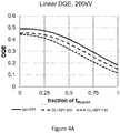
- FIG. 4Ais a graph showing detective quantum efficiency (DQE) for ideal, front, and back illuminated imaging sensors
- FIG. 4Bis a graph comparing DQE for front versus back illuminated imaging sensors to the ideal sensor DQE curve in FIG. 4A ;
- FIGS. 5A-Care cross sections of processing stages for an exemplary silicon imaging detector according to embodiments described herein;
- FIGS. 6A-Care cross sections of processing stages for an exemplary silicon imaging detector according to embodiments described herein.
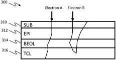
- an active pixel silicon imaging detector 300comprises a SUB layer 310 , an EPI layer 312 , a BEOL layer 314 , and a thermal conduction layer (“TCL”) 316 .
- TCL 316is applied to the BEOL layer 314 after manufacture of the BEOL layer.
- detector 300is exposed to incoming electrons initially from the substrate side 310 , i.e., the sensor is “back-illuminated.” The sensor is back-illuminated because some scattering also occurs in the BEOL, which, in a front-illuminated configuration, lies in front of the detection EPI layer.
- pre-detection scatter by the BEOLhas little or no effect on the number of detections per incoming electron, the scatter may reduce the spatial correlation between entry point and detection point and may therefore limit the ultimate resolution of the detector.
- the BEOLcannot be removed as it performs the necessary readout function of the detector.
- back-illuminationplaces the BEOL after the EPI detection layer and eliminates the pre-detection scatter caused by the BEOL.
- the thermal conduction layer 316is designed both in thickness and material composition to have a high thermal conductivity but a low propensity to reflect electrons back into the EPI detection layer 312 .
- Prior art substrate thicknesshas been in the range of 10 um to 40 um yielding backscatter fractions from less than 2% to more than 10% for 200 kV and 300 kV electrons. It would be advantageous to reduce that backscatter fraction through reduced Z (atomic number) of the thermal conduction substrate or by reducing the thickness which would be possible with a higher thermal conductivity. In practice materials vary by both these parameters simultaneously. As shown in FIG.
- Electron Apasses out of the TCL layer 316 without being reflected back into the sensor. Electron B is reflected by the TCL layer and detected a second time in the detection layer 312 .
- the thickness of the TCL layer and its compositiondetermine the likelihood of electrons passing through the TCL layer or being reflected back into the sensor 300 .
- FIG. 4Ashows simulated linear detective quantum efficiency (DQE) for three configurations: the solid curve is for an idealized epitaxial layer only (“just EPI”), the middle curve (large dashes) is for a back side illuminated device having a BEOL and epitaxial layer wherein the epitaxial layer is exposed to the electrons directly and the lower curve (short dashes) is for a front side illuminated device having a BEOL and an epitaxial layer (i.e., illuminated through the BEOL).
- FIG. 4Bshow simulated ratios of the DQE for the two sensors of FIG. 4A having a BEOL, as compared to the idealized epitaxial layer only sensor curve of FIG. 4A .
- Both graphsshow performance as quantified by linear DQE vs. spatial frequency.
- Zero spatial frequency at the origin on the left of each graphcorresponds to performance of the detector functioning as a whole.
- Spatial frequency of one times the Nyquist frequency at the right of each graphshows performance for modulations of image signal which go high and low every other pixel. This is the highest spatial modulation frequency that can be acquired by a pixelated detector without aliasing errors.
- FIGS. 4A and 4Bshow that while material on both the entrance and exit faces of the detector increases scatter at increasing levels of spatial frequency, the scatter that occurs post-detection from material mounted on the exit face (large dash curve in both graphs) is less damaging to high-resolution signal quality.
- the simulation resultsalso imply that any material in front of the EPI detection layer should be minimized. Exposing the sensor from the back side as in FIG. 3 leaves substrate in front of the epitaxial layer.
- the conclusion from FIGS. 4A and 4Bis that anything in front of the EPI detection layer reduces DQE, which means that all or most of the substrate (leaving no more than 5 microns), now at the entrance surface, should be removed.
- a thermal conduction layercan support the EPI and BEOL layers from the BEOL layer side (i.e. the exit side in a back-side illuminated configuration). Supporting the device with a layer next to the BEOL layer enables complete removal of the original substrate layer. This in turn allows for direct exposure of the EPI layer, which heretofore has not been possible.
- thermal conduction layeris not part of the original sensor fabrication (i.e. not part of the growth of the epitaxial layer or the deposition of the BEOL layer), there is an opportunity to find a thermal layer material better than silicon (which comprises the original substrate and most of the heat removal in prior art devices) for the purpose.
- the thermal conductivity layer materialcan be better than the original silicon substrate in two ways. It can have a better thermal conductivity and it can have a lower tendency to scatter electrons.
- the benefit of the combined effectsis proportional to thermal conductivity ⁇ and inversely proportional to the square of atomic number Z.
- the following tablesummarizes estimates of ⁇ , Z and Q for some representative materials.
- the estimates of ⁇ and therefore also of Qare subject to manufacturing method, binder fraction, etc.
- the tableis not meant to be exhaustive but illustrative of the principal used for identifying materials as more or less suited for an electron-transmissive thermal conductive layer as/than silicon.
- thermal conduction layerDue to the fragility of the thin EPI detector layer, especially after removal of all substrate material, methods for attachment of a thermally conductive layer to the thin device must either be very low force/pressure or a robust temporary support for the thin layers must be provided as part of any higher pressure process step. Methods for affixing a thermal conduction layer to the BEOL of the back-illuminated sensor vary depending on the conduction material.
- Solid refractory dielectricsincluding but not limited to boron nitride, beryllium oxide and diamond can be contact bonded onto the sensor BEOL either with or without temperature elevation and with or without applied pressure, followed by removal of excess thermal conduction layer material and also removal of the silicon substrate layer. Contact bonding is described in U.S. Pat. Nos. 5,852,622 and 5,441,803, which are incorporated by reference herein. The substrate is left intact at first, to allow pressure applied for contact bonding of the thermal layer to the BEOL.
- FIGS. 5A-5Cshow cross sections of the manufacturing process for an imaging sensor according to an aspect of the invention.
- FIG. 5Ashows a sensor 510 comprising a silicon substrate 512 , an epitaxial layer 514 and a BEOL 516 .
- FIG. 5Aalso shows a thermal conduction layer 520 supported by a thermal conduction layer substrate 522 .
- the TCL substrate 522can be the same or different material as the TCL itself.
- FIG. 5Bshows the bonding of the BEOL 516 of the sensor 510 to the thermal conduction layer 520 .
- both the imaging sensor 510 and the thermal conduction layerare supported by substrates 512 , 522 to allow pressure to be applied in a contact bonding process.
- FIG. 5Cshows the completed imaging sensor 510 with the original sensor substrate 512 removed and the thermal conduction layer substrate 522 removed. Removal of substrate material or excess thermal conduction material can be accomplished by a variety of means including, but not limited to, polishing, chemo-mechanical polishing, ion milling, and laser ablation.
- the resulting sensor shown in FIG. 5Chas an unhindered epitaxial sensing layer 514 that can be directly exposed to electrons without any initial scattering, plus a thermal conduction layer 520 to remove heat from the device as well as physically support the device.
- the thermal conduction layer to be contact bonded to the sensorcan be derived from a variety of initial starting forms and processed in a variety of ways. Consistent with embodiments described herein, the TCL/SUB layer 502 / 522 bonded to the BEOL can be made of a single material which is thicker than the final TCL 520 . The extra thickness is necessary for strength in the bonding process. The layer is contact bonded onto the BEOL layer of the sensor and the extra material is polished off. In this case the ultimate thickness of the thermal conduction layer is determined by close monitoring of the thickness during polishing.
- a single material thicker than the final thermal conduction layeris used as a starting material, but the starting material is ion-implanted on the side to be bonded to a predetermined depth.
- This ion implantationchanges the etch rate for a chemical or chemo-mechanical thinning process without changing the thermal or scattering properties of the thermal conduction layer material.
- the thermal conduction materialis thinned. The etch stop created by the ion implantation increases the reliability of achieving a given thickness thermal conduction layer.
- the thermal conduction layeris epitaxially grown or chemical vapor deposited onto a substrate of a different material than the grown or deposited layer.
- the substrateis used as a transfer layer.
- the combined layersare contact bonded to the BEOL layer as above. Once bonded to the BEOL layer the substrate material is removed by one or more of the processes described above.
- a thermally conductive powder layeris sintered onto a substrate of similar melting point and coefficient of thermal expansion as the powder.
- the substrateacting as a transfer layer.
- the combined layersare contact bonded to the BEOL layer, followed by complete removal of the substrate material after contact bonding.
- FIGS. 6A-Cshow cross sections of an exemplary sputtering deposition of a thermal conduction layer 616 onto a BEOL 614 .
- FIG. 6Ashows a sensor 610 comprising an epitaxial layer 612 and a BEOL 614 .
- the original substrate on which the sensor was developedhas already been removed in this embodiment.
- FIG. 6Bshows the sputtering of material onto the BEOL to create a thermal conduction layer 616 .
- FIG. 6Cshows a completed sensor with a fully deposited thermal conduction layer 616 ,
- Powder-based materialscan be applied by settling or slurry coating processes in a solvent-thinned binder such as is done for powder phosphor scintillators.
- the powder-binder mixtureis applied to the BEOL layer by means including silk screening or gravitational settling.
- a liquid powder suspensionmay also be spin coated onto the BEOL layer.
- Exemplary bindersinclude but are not limited to sodium silicate, ethyl cellulose, and ammonium polymethacrylate, and cellulose nitrate. While a binder sacrifices some of the thermal conductivity, given the extremely high conductivity of a graphite or boron nitride powder and given sufficiently low binder fraction, the net conductivity will still constitute an improvement over silicon.
- Powder-based thermal conductorscan also be deposited directly onto the BEOL layer by spin-coating of a liquid powder suspension.
- the starting material for a thermal conductor layeris a flexible sheet comprising a flexible polymer embedding medium for powder heat conduction material.
- the flexible sheet materialcan be contact bonded in vacuum to prevent gas entrapment, with or without temperature elevation.
- the materialshould be affixed to the BEOL layer after all high-temperature processes are complete on the sensor itself. In this case attachment is performed on a fragile, thin final sensor with only BEOL and epitaxial layers remaining. Thus attachment will need to use only low forces/pressures.
- Possible low force attachment methodsinclude but are not limited to: directing a gas jet at outer surface of the flexible layer to press and smooth the layer along with low temperature heating to maximize the flexibility and adhesion of the flexible layer.
- a warm gas jetcombines the two effects of smoothing and heating.
- centrifugal forceis used to flatten the flexible sheet during adhesion to the BEOL layer of the sensor.
- electrostatic-dielectric attractionis used with due care to prevent electrostatic damage to the sensor.
- Some types of flexible sheetsare conductive (graphite-containing for instance) and others are electrically insulating (boron-nitride for instance) and may require different handling in an electrostatic method of attachment.
- Powder-based thermal conductorscan be deposited directly onto the BEOL layer by settling or slurry coating in a solvent-thinned binder as is done for powder phosphor scintillators.
- exemplary bindersinclude but are not limited to sodium silicate, ethyl cellulose, and ammonium polymethacrylate, and cellulose nitrate. While a binder sacrifices some of the thermal conductivity, given the extremely high conductivity of a graphite or boron nitride powder and given sufficiently low binder fraction, the net conductivity will still constitute an improvement over silicon.
- Powder-based thermal conductorscan also be deposited directly onto the BEOL layer by spin-coating of a liquid powder suspension.
Landscapes
- Physics & Mathematics (AREA)
- Health & Medical Sciences (AREA)
- Life Sciences & Earth Sciences (AREA)
- Chemical & Material Sciences (AREA)
- Analytical Chemistry (AREA)
- Biochemistry (AREA)
- General Health & Medical Sciences (AREA)
- General Physics & Mathematics (AREA)
- Immunology (AREA)
- Pathology (AREA)
- Solid State Image Pick-Up Elements (AREA)
- Measurement Of Radiation (AREA)
Abstract
Description
- This application claims priority under 35 U.S.C. § 119, based on U.S. Provisional Application No. 62/952,852, filed Dec. 23, 2019, the disclosure of which is hereby incorporated by reference herein.
- Electron imaging detectors based on thinned transmission silicon active pixel sensors have revolutionized cryo-electron microscopy. These devices have enabled scientists to investigate the structure of large biological macromolecules at levels not achieved previously. Because these are transmission devices, electrons which have interacted with the detection layer ideally exit the sensor without being scattered back into the detection layer. The use of silicon as the sensor substrate minimizes the scatter of electrons within the sensor back into the detection layer. Active sensors maximize the signal to noise ratio for detecting positions of individual incoming electrons through amplification of electron signals.
- As shown in
FIG. 1 , anactive pixel sensor 10 is built up in three layers: a substrate (SUB)layer 12, an epitaxially grown detection (EPI)layer 14, and a back-end-of-line (BEOL)layer 16.SUB layer 12 is inert from the standpoint of detecting electrons and is used as the base on which to form the detection layers.EPI layer 14 includes a material that generates sensor electrons in response to incoming electron microscope electrons. These sensor electrons are collected.BEOL layer 16 is provided aboveEPI layer 14 and contains metal interconnects and oxide insulation for reading out the sensor. - In some known electron imaging detectors,
SUB layer 12 is thick enough that no electrons pass all the way through it. Two example electron paths are shown inFIG. 1 . Electrons paths A and B are scattered by the substrate back into theEPI detection layer 14 and are detected a second time atlocations EPI layer 14. This extra detection reduces imaging quality. ThinningSUB layer 12 from the back can reduce backscatter and the secondary detections, as shown inFIG. 2 , where electron A does not backscatter up into thedetection layer 14. - In the example image using the same electron paths, in
FIG. 2 , electron A, which penetrated the substrate layer to greater depth, is no longer scattered back to the detection layer. Electron B, which is scattered at a shallower depth, still returns to the detection layer. Backscatter can be minimized by minimizing the amount of substrate in this front-illuminated configuration. - Thinning the substrate reduces the available material for removal of heat from the device. As the number of pixels per a given area is increased by advances in process technology, heat removal becomes an ever greater problem.
FIG. 1 is a cross section of a prior art silicon imaging detector;FIG. 2 is cross section of another prior art silicon imaging detector;FIG. 3 is a cross section of an exemplary silicon imaging detector according to implementations described herein;FIG. 4A is a graph showing detective quantum efficiency (DQE) for ideal, front, and back illuminated imaging sensors;FIG. 4B is a graph comparing DQE for front versus back illuminated imaging sensors to the ideal sensor DQE curve inFIG. 4A ;FIGS. 5A-C are cross sections of processing stages for an exemplary silicon imaging detector according to embodiments described herein; andFIGS. 6A-C are cross sections of processing stages for an exemplary silicon imaging detector according to embodiments described herein.- Those skilled in the art will recognize other detailed designs and methods that can be developed employing the teachings of the present invention. The examples provided here are illustrative and do not limit the scope of the invention, which is defined by the attached claims. The following detailed description refers to the accompanying drawings. The same reference numbers in different drawings may identify the same or similar elements.
- In accordance with embodiments described herein, as shown in
FIG. 3 , an active pixelsilicon imaging detector 300 comprises aSUB layer 310, anEPI layer 312, aBEOL layer 314, and a thermal conduction layer (“TCL”)316. TCL316 is applied to theBEOL layer 314 after manufacture of the BEOL layer. Consistent with embodiments described herein,detector 300 is exposed to incoming electrons initially from thesubstrate side 310, i.e., the sensor is “back-illuminated.” The sensor is back-illuminated because some scattering also occurs in the BEOL, which, in a front-illuminated configuration, lies in front of the detection EPI layer. While pre-detection scatter by the BEOL has little or no effect on the number of detections per incoming electron, the scatter may reduce the spatial correlation between entry point and detection point and may therefore limit the ultimate resolution of the detector. The BEOL cannot be removed as it performs the necessary readout function of the detector. However, back-illumination places the BEOL after the EPI detection layer and eliminates the pre-detection scatter caused by the BEOL. - As shown in
FIG. 3 , electrons A and B are detected in theEPI layer 312 and then pass through theBEOL layer 314. Thethermal conduction layer 316 is designed both in thickness and material composition to have a high thermal conductivity but a low propensity to reflect electrons back into theEPI detection layer 312. Prior art substrate thickness has been in the range of 10 um to 40 um yielding backscatter fractions from less than 2% to more than 10% for 200 kV and 300 kV electrons. It would be advantageous to reduce that backscatter fraction through reduced Z (atomic number) of the thermal conduction substrate or by reducing the thickness which would be possible with a higher thermal conductivity. In practice materials vary by both these parameters simultaneously. As shown inFIG. 3 , Electron A, passes out of theTCL layer 316 without being reflected back into the sensor. Electron B is reflected by the TCL layer and detected a second time in thedetection layer 312. The thickness of the TCL layer and its composition determine the likelihood of electrons passing through the TCL layer or being reflected back into thesensor 300. FIG. 4A shows simulated linear detective quantum efficiency (DQE) for three configurations: the solid curve is for an idealized epitaxial layer only (“just EPI”), the middle curve (large dashes) is for a back side illuminated device having a BEOL and epitaxial layer wherein the epitaxial layer is exposed to the electrons directly and the lower curve (short dashes) is for a front side illuminated device having a BEOL and an epitaxial layer (i.e., illuminated through the BEOL).FIG. 4B show simulated ratios of the DQE for the two sensors ofFIG. 4A having a BEOL, as compared to the idealized epitaxial layer only sensor curve ofFIG. 4A .- Both graphs (
FIGS. 4A, 4B ) show performance as quantified by linear DQE vs. spatial frequency. Zero spatial frequency at the origin on the left of each graph corresponds to performance of the detector functioning as a whole. Spatial frequency of one times the Nyquist frequency at the right of each graph shows performance for modulations of image signal which go high and low every other pixel. This is the highest spatial modulation frequency that can be acquired by a pixelated detector without aliasing errors. FIGS. 4A and 4B show that while material on both the entrance and exit faces of the detector increases scatter at increasing levels of spatial frequency, the scatter that occurs post-detection from material mounted on the exit face (large dash curve in both graphs) is less damaging to high-resolution signal quality. The simulation results also imply that any material in front of the EPI detection layer should be minimized. Exposing the sensor from the back side as inFIG. 3 leaves substrate in front of the epitaxial layer. The conclusion fromFIGS. 4A and 4B is that anything in front of the EPI detection layer reduces DQE, which means that all or most of the substrate (leaving no more than 5 microns), now at the entrance surface, should be removed. Up to now this has been impractical due to the role played by the substrate in providing mechanical support and heat conduction for the sensor. Consistent with embodiments herein, a thermal conduction layer can support the EPI and BEOL layers from the BEOL layer side (i.e. the exit side in a back-side illuminated configuration). Supporting the device with a layer next to the BEOL layer enables complete removal of the original substrate layer. This in turn allows for direct exposure of the EPI layer, which heretofore has not been possible.- Because the thermal conduction layer is not part of the original sensor fabrication (i.e. not part of the growth of the epitaxial layer or the deposition of the BEOL layer), there is an opportunity to find a thermal layer material better than silicon (which comprises the original substrate and most of the heat removal in prior art devices) for the purpose. The thermal conductivity layer material can be better than the original silicon substrate in two ways. It can have a better thermal conductivity and it can have a lower tendency to scatter electrons. The benefit of the combined effects is proportional to thermal conductivity κ and inversely proportional to the square of atomic number Z. A heuristic quality factor for the purpose of an electron-transmissive thermal conduction layer can be defined as Q=κ/Z2. The following table summarizes estimates of κ, Z and Q for some representative materials. The estimates of κ and therefore also of Q are subject to manufacturing method, binder fraction, etc. The table is not meant to be exhaustive but illustrative of the principal used for identifying materials as more or less suited for an electron-transmissive thermal conductive layer as/than silicon.
TABLE 1 min thermal stoichiometric conductivity average atomic quality factor Material (W/mK) number (Z) Q = κ/Z2 aluminum 170 13 1.01 aluminum nitride 180 10 1.80 diamond 1000 6 27.78 pyrolized graphite 700 6 19.44 beryllium 200 4 12.50 beryllium oxide 265 6 7.36 boron nitride 1700 6 47.22 silicon 190 14 0.97 - Due to the fragility of the thin EPI detector layer, especially after removal of all substrate material, methods for attachment of a thermally conductive layer to the thin device must either be very low force/pressure or a robust temporary support for the thin layers must be provided as part of any higher pressure process step. Methods for affixing a thermal conduction layer to the BEOL of the back-illuminated sensor vary depending on the conduction material.
- Solid refractory dielectrics, including but not limited to boron nitride, beryllium oxide and diamond can be contact bonded onto the sensor BEOL either with or without temperature elevation and with or without applied pressure, followed by removal of excess thermal conduction layer material and also removal of the silicon substrate layer. Contact bonding is described in U.S. Pat. Nos. 5,852,622 and 5,441,803, which are incorporated by reference herein. The substrate is left intact at first, to allow pressure applied for contact bonding of the thermal layer to the BEOL.
FIGS. 5A-5C show cross sections of the manufacturing process for an imaging sensor according to an aspect of the invention.FIG. 5A shows asensor 510 comprising asilicon substrate 512, anepitaxial layer 514 and aBEOL 516.FIG. 5A also shows athermal conduction layer 520 supported by a thermalconduction layer substrate 522. TheTCL substrate 522 can be the same or different material as the TCL itself.FIG. 5B shows the bonding of theBEOL 516 of thesensor 510 to thethermal conduction layer 520. At this stage, both theimaging sensor 510 and the thermal conduction layer are supported bysubstrates FIG. 5C shows the completedimaging sensor 510 with theoriginal sensor substrate 512 removed and the thermalconduction layer substrate 522 removed. Removal of substrate material or excess thermal conduction material can be accomplished by a variety of means including, but not limited to, polishing, chemo-mechanical polishing, ion milling, and laser ablation. The resulting sensor shown inFIG. 5C has an unhinderedepitaxial sensing layer 514 that can be directly exposed to electrons without any initial scattering, plus athermal conduction layer 520 to remove heat from the device as well as physically support the device.- The thermal conduction layer to be contact bonded to the sensor can be derived from a variety of initial starting forms and processed in a variety of ways. Consistent with embodiments described herein, the TCL/SUB layer502/522 bonded to the BEOL can be made of a single material which is thicker than the
final TCL 520. The extra thickness is necessary for strength in the bonding process. The layer is contact bonded onto the BEOL layer of the sensor and the extra material is polished off. In this case the ultimate thickness of the thermal conduction layer is determined by close monitoring of the thickness during polishing. - In a further embodiment, a single material thicker than the final thermal conduction layer is used as a starting material, but the starting material is ion-implanted on the side to be bonded to a predetermined depth. This ion implantation changes the etch rate for a chemical or chemo-mechanical thinning process without changing the thermal or scattering properties of the thermal conduction layer material. Once bonded to the BEOL layer, the thermal conduction material is thinned. The etch stop created by the ion implantation increases the reliability of achieving a given thickness thermal conduction layer.
- In a further embodiment, the thermal conduction layer is epitaxially grown or chemical vapor deposited onto a substrate of a different material than the grown or deposited layer. The substrate is used as a transfer layer. The combined layers are contact bonded to the BEOL layer as above. Once bonded to the BEOL layer the substrate material is removed by one or more of the processes described above.
- In a further embodiment, a thermally conductive powder layer is sintered onto a substrate of similar melting point and coefficient of thermal expansion as the powder. The substrate acting as a transfer layer. The combined layers are contact bonded to the BEOL layer, followed by complete removal of the substrate material after contact bonding.
- Metal layers can be sputtered onto the BEOL.
FIGS. 6A-C show cross sections of an exemplary sputtering deposition of a thermal conduction layer616 onto a BEOL614.FIG. 6A shows a sensor610 comprising an epitaxial layer612 and a BEOL614. The original substrate on which the sensor was developed has already been removed in this embodiment.FIG. 6B shows the sputtering of material onto the BEOL to create a thermal conduction layer616.FIG. 6C shows a completed sensor with a fully deposited thermal conduction layer616, - Powder-based materials can be applied by settling or slurry coating processes in a solvent-thinned binder such as is done for powder phosphor scintillators. The powder-binder mixture is applied to the BEOL layer by means including silk screening or gravitational settling. A liquid powder suspension may also be spin coated onto the BEOL layer. Exemplary binders include but are not limited to sodium silicate, ethyl cellulose, and ammonium polymethacrylate, and cellulose nitrate. While a binder sacrifices some of the thermal conductivity, given the extremely high conductivity of a graphite or boron nitride powder and given sufficiently low binder fraction, the net conductivity will still constitute an improvement over silicon.
- Powder-based thermal conductors can also be deposited directly onto the BEOL layer by spin-coating of a liquid powder suspension.
- In a further embodiment, the starting material for a thermal conductor layer is a flexible sheet comprising a flexible polymer embedding medium for powder heat conduction material. The flexible sheet material can be contact bonded in vacuum to prevent gas entrapment, with or without temperature elevation. The material should be affixed to the BEOL layer after all high-temperature processes are complete on the sensor itself. In this case attachment is performed on a fragile, thin final sensor with only BEOL and epitaxial layers remaining. Thus attachment will need to use only low forces/pressures. Possible low force attachment methods include but are not limited to: directing a gas jet at outer surface of the flexible layer to press and smooth the layer along with low temperature heating to maximize the flexibility and adhesion of the flexible layer. A warm gas jet combines the two effects of smoothing and heating. In a further embodiment, centrifugal force is used to flatten the flexible sheet during adhesion to the BEOL layer of the sensor. In a further embodiment electrostatic-dielectric attraction is used with due care to prevent electrostatic damage to the sensor. Some types of flexible sheets are conductive (graphite-containing for instance) and others are electrically insulating (boron-nitride for instance) and may require different handling in an electrostatic method of attachment.
- Powder-based thermal conductors can be deposited directly onto the BEOL layer by settling or slurry coating in a solvent-thinned binder as is done for powder phosphor scintillators. Exemplary binders include but are not limited to sodium silicate, ethyl cellulose, and ammonium polymethacrylate, and cellulose nitrate. While a binder sacrifices some of the thermal conductivity, given the extremely high conductivity of a graphite or boron nitride powder and given sufficiently low binder fraction, the net conductivity will still constitute an improvement over silicon.
- Powder-based thermal conductors can also be deposited directly onto the BEOL layer by spin-coating of a liquid powder suspension.
- Although the invention has been described in detail above, it is expressly understood that it will be apparent to persons skilled in the relevant art that the invention may be modified without departing from the spirit of the invention. Various changes of form, design, or arrangement may be made to the invention without departing from the spirit and scope of the invention. Therefore, the above-mentioned description is to be considered exemplary, rather than limiting, and the true scope of the invention is that defined in the following claims.
- No element, act, or instruction used in the description of the present application should be construed as critical or essential to the invention unless explicitly described as such. Also, as used herein, the article “a” is intended to include one or more items. Further, the phrase “based on” is intended to mean “based, at least in part, on” unless explicitly stated otherwise.
Claims (19)
Priority Applications (2)
| Application Number | Priority Date | Filing Date | Title |
|---|---|---|---|
| US17/130,666US12057515B2 (en) | 2019-12-23 | 2020-12-22 | Electronic imaging detector with thermal conduction layer |
| US18/761,587US20240355943A1 (en) | 2019-12-23 | 2024-07-02 | Electronic imaging detector with thermal conduction layer |
Applications Claiming Priority (2)
| Application Number | Priority Date | Filing Date | Title |
|---|---|---|---|
| US201962952852P | 2019-12-23 | 2019-12-23 | |
| US17/130,666US12057515B2 (en) | 2019-12-23 | 2020-12-22 | Electronic imaging detector with thermal conduction layer |
Related Child Applications (1)
| Application Number | Title | Priority Date | Filing Date |
|---|---|---|---|
| US18/761,587ContinuationUS20240355943A1 (en) | 2019-12-23 | 2024-07-02 | Electronic imaging detector with thermal conduction layer |
Publications (2)
| Publication Number | Publication Date |
|---|---|
| US20210193848A1true US20210193848A1 (en) | 2021-06-24 |
| US12057515B2 US12057515B2 (en) | 2024-08-06 |
Family
ID=73856081
Family Applications (2)
| Application Number | Title | Priority Date | Filing Date |
|---|---|---|---|
| US17/130,666Active2041-03-25US12057515B2 (en) | 2019-12-23 | 2020-12-22 | Electronic imaging detector with thermal conduction layer |
| US18/761,587PendingUS20240355943A1 (en) | 2019-12-23 | 2024-07-02 | Electronic imaging detector with thermal conduction layer |
Family Applications After (1)
| Application Number | Title | Priority Date | Filing Date |
|---|---|---|---|
| US18/761,587PendingUS20240355943A1 (en) | 2019-12-23 | 2024-07-02 | Electronic imaging detector with thermal conduction layer |
Country Status (4)
| Country | Link |
|---|---|
| US (2) | US12057515B2 (en) |
| EP (1) | EP3843141A1 (en) |
| JP (2) | JP7478657B2 (en) |
| CN (2) | CN119574544A (en) |
Citations (13)
| Publication number | Priority date | Publication date | Assignee | Title |
|---|---|---|---|---|
| JPH06318690A (en)* | 1993-05-07 | 1994-11-15 | Hamamatsu Photonics Kk | Semiconductor energy beam detector and its manufacture |
| JPH06350068A (en)* | 1993-06-03 | 1994-12-22 | Hamamatsu Photonics Kk | Method for manufacturing semiconductor energy ray detector |
| US5441803A (en)* | 1988-08-30 | 1995-08-15 | Onyx Optics | Composites made from single crystal substances |
| US5852622A (en)* | 1988-08-30 | 1998-12-22 | Onyx Optics, Inc. | Solid state lasers with composite crystal or glass components |
| US20110089517A1 (en)* | 2009-10-20 | 2011-04-21 | Omnivision Technologies, Inc. | Cmos image sensor with heat management structures |
| US20130183792A1 (en)* | 2012-01-18 | 2013-07-18 | Kabushiki Kaisha Toshiba | Method for manufacturing semiconductor device |
| US20130264481A1 (en)* | 2012-04-10 | 2013-10-10 | Kla-Tencor Corporation | Back-Illuminated Sensor With Boron Layer |
| US20140291790A1 (en)* | 2013-04-01 | 2014-10-02 | Industrial Technology Research Institute | Encapsulation of backside illumination photosensitive device |
| US9397134B1 (en)* | 2013-02-07 | 2016-07-19 | Google Inc. | Methods and devices configured to provide selective heat transfer of an integrated circuit |
| US20170104019A1 (en)* | 2015-10-12 | 2017-04-13 | Samsung Electronics Co., Ltd. | Image sensor and method of manufacturing the same |
| US20170356953A1 (en)* | 2016-06-14 | 2017-12-14 | Taiwan Semiconductor Manufacturing Co., Ltd. | In-line device electrical property estimating method and test structure of the same |
| US20180277530A1 (en)* | 2015-03-09 | 2018-09-27 | Monolithic 3D Inc. | Methods for processing a 3d semiconductor device |
| WO2021014849A1 (en)* | 2019-07-24 | 2021-01-28 | ソニーセミコンダクタソリューションズ株式会社 | Solid-state imaging device, electronic machine and solid-state imaging device production method |
Family Cites Families (15)
| Publication number | Priority date | Publication date | Assignee | Title |
|---|---|---|---|---|
| JPH02153849A (en)* | 1988-08-30 | 1990-06-13 | Hoya Opt Inc | Composite consisting of glass-containing substance and glass-free substance, and method for forming said composite |
| JP2003204057A (en)* | 2002-01-10 | 2003-07-18 | Nikon Corp | Back-illuminated imaging device, aberration measurement device, position measurement device, projection exposure device, method of manufacturing back-illuminated imaging device, and device manufacturing method |
| JP4747704B2 (en) | 2005-07-20 | 2011-08-17 | 豊田合成株式会社 | Method for manufacturing light emitting device with phosphor layer |
| JP2008226553A (en) | 2007-03-09 | 2008-09-25 | Electric Power Dev Co Ltd | Dye-sensitized solar cell sealing part and dye-sensitized solar cell |
| JP4796030B2 (en)* | 2007-09-27 | 2011-10-19 | 富士フイルム株式会社 | Image detector and image capturing system |
| JP5194862B2 (en)* | 2008-02-12 | 2013-05-08 | 株式会社島津製作所 | 2D image detector |
| US20100159632A1 (en)* | 2008-12-23 | 2010-06-24 | Omnivision Technologies, Inc. | Technique for fabrication of backside illuminated image sensor |
| EP2346094A1 (en)* | 2010-01-13 | 2011-07-20 | FEI Company | Method of manufacturing a radiation detector |
| JP2012049493A (en)* | 2010-01-29 | 2012-03-08 | Nitto Denko Corp | Imaging part |
| US9123608B2 (en)* | 2011-12-09 | 2015-09-01 | Taiwan Semiconductor Manufacturing Company, Ltd. | Backside illuminated CMOS image sensor |
| US10014292B2 (en)* | 2015-03-09 | 2018-07-03 | Monolithic 3D Inc. | 3D semiconductor device and structure |
| US10490588B2 (en)* | 2016-09-16 | 2019-11-26 | Semiconductor Components Industries, Llc | Methods and apparatus for a thermal equalizer in an image sensor |
| CN109346489A (en)* | 2018-09-20 | 2019-02-15 | 德淮半导体有限公司 | Image sensor and method of manufacturing the same |
| CN109326621B (en)* | 2018-10-17 | 2021-02-09 | 德淮半导体有限公司 | Method of forming image sensor and image sensor |
| CN110211984A (en)* | 2019-06-20 | 2019-09-06 | 德淮半导体有限公司 | Stacked back side illumination image sensor and its manufacturing method |
- 2020
- 2020-12-21EPEP20215917.4Apatent/EP3843141A1/enactivePending
- 2020-12-21JPJP2020211887Apatent/JP7478657B2/enactiveActive
- 2020-12-22CNCN202411701392.4Apatent/CN119574544A/enactivePending
- 2020-12-22CNCN202011524890.8Apatent/CN113092464B/enactiveActive
- 2020-12-22USUS17/130,666patent/US12057515B2/enactiveActive
- 2023
- 2023-01-10JPJP2023001663Apatent/JP2023052734A/enactivePending
- 2024
- 2024-07-02USUS18/761,587patent/US20240355943A1/enactivePending
Patent Citations (13)
| Publication number | Priority date | Publication date | Assignee | Title |
|---|---|---|---|---|
| US5441803A (en)* | 1988-08-30 | 1995-08-15 | Onyx Optics | Composites made from single crystal substances |
| US5852622A (en)* | 1988-08-30 | 1998-12-22 | Onyx Optics, Inc. | Solid state lasers with composite crystal or glass components |
| JPH06318690A (en)* | 1993-05-07 | 1994-11-15 | Hamamatsu Photonics Kk | Semiconductor energy beam detector and its manufacture |
| JPH06350068A (en)* | 1993-06-03 | 1994-12-22 | Hamamatsu Photonics Kk | Method for manufacturing semiconductor energy ray detector |
| US20110089517A1 (en)* | 2009-10-20 | 2011-04-21 | Omnivision Technologies, Inc. | Cmos image sensor with heat management structures |
| US20130183792A1 (en)* | 2012-01-18 | 2013-07-18 | Kabushiki Kaisha Toshiba | Method for manufacturing semiconductor device |
| US20130264481A1 (en)* | 2012-04-10 | 2013-10-10 | Kla-Tencor Corporation | Back-Illuminated Sensor With Boron Layer |
| US9397134B1 (en)* | 2013-02-07 | 2016-07-19 | Google Inc. | Methods and devices configured to provide selective heat transfer of an integrated circuit |
| US20140291790A1 (en)* | 2013-04-01 | 2014-10-02 | Industrial Technology Research Institute | Encapsulation of backside illumination photosensitive device |
| US20180277530A1 (en)* | 2015-03-09 | 2018-09-27 | Monolithic 3D Inc. | Methods for processing a 3d semiconductor device |
| US20170104019A1 (en)* | 2015-10-12 | 2017-04-13 | Samsung Electronics Co., Ltd. | Image sensor and method of manufacturing the same |
| US20170356953A1 (en)* | 2016-06-14 | 2017-12-14 | Taiwan Semiconductor Manufacturing Co., Ltd. | In-line device electrical property estimating method and test structure of the same |
| WO2021014849A1 (en)* | 2019-07-24 | 2021-01-28 | ソニーセミコンダクタソリューションズ株式会社 | Solid-state imaging device, electronic machine and solid-state imaging device production method |
Also Published As
| Publication number | Publication date |
|---|---|
| CN119574544A (en) | 2025-03-07 |
| CN113092464B (en) | 2024-12-13 |
| EP3843141A1 (en) | 2021-06-30 |
| JP7478657B2 (en) | 2024-05-07 |
| JP2021100118A (en) | 2021-07-01 |
| US20240355943A1 (en) | 2024-10-24 |
| CN113092464A (en) | 2021-07-09 |
| JP2023052734A (en) | 2023-04-12 |
| US12057515B2 (en) | 2024-08-06 |
Similar Documents
| Publication | Publication Date | Title |
|---|---|---|
| US6025585A (en) | Low-resistivity photon-transparent window attached to photo-sensitive silicon detector | |
| EP0883189B1 (en) | Back illuminated photodetector and method of fabricating the same | |
| KR102302636B1 (en) | Scanning electron microscope and methods of inspecting and reviewing samples | |
| CA2081306C (en) | Semiconductor film bolometer thermal infrared detector | |
| WO1998020561A9 (en) | Low-resistivity photon-transparent window attached to photo-sensitive silicon detector | |
| US20190280042A1 (en) | Monolithic silicon pixel detector, and systems and methods for particle detection | |
| US9123622B2 (en) | Atomic layer deposition of high performance anti reflection coatings on delta-doped CCDs | |
| US12057515B2 (en) | Electronic imaging detector with thermal conduction layer | |
| US20150340402A1 (en) | Photodiode array | |
| Siegmund | Advances in microchannel plate detectors for UV/visible astronomy | |
| Ryu et al. | Development of CCDs for REXIS on OSIRIS-REx | |
| US9640680B1 (en) | Wide-band transparent electrical contacts and interconnects for FPAS and a method of making the same | |
| Siegmund et al. | Development of large area photon counting detectors optimized for Cherenkov light imaging with high temporal and sub-mm spatial resolution | |
| US20220082713A1 (en) | multi-purpose high-energy particle sensor array and method of making the same for high-resolution imaging | |
| CA2612058C (en) | Electron bombarded image sensor array device and its manufactoring method | |
| JP2010044074A (en) | Electromagnetic radiation detection device, and method of manufacturing the same | |
| TWI894458B (en) | Solid state device for wafer inspection, and electron detection system | |
| Luppino et al. | CCD mosaic development for large optical telescopes | |
| CN116888704B (en) | Segmented multichannel back-illuminated solid-state detector with through-holes for detecting secondary and backscattered electrons | |
| JP2001305234A (en) | Semiconductor electron beam detector | |
| WO2004012241A2 (en) | Radiation hardened visible p-i-n detector | |
| JP2023540492A (en) | High DQE direct detection image sensor for electronics with 40-120KEV energy | |
| JPWO2021207435A5 (en) | ||
| Kok et al. | 3D detector activities at SINTEF MiNaLab–Wafer bonding and deep reactive Ion Etching | |
| Hemphill et al. | Development of Large Area Photon Counting Detectors Optimized for Cherenkov Light Imaging with High Temporal and sub-mm Spatial Resolution |
Legal Events
| Date | Code | Title | Description |
|---|---|---|---|
| FEPP | Fee payment procedure | Free format text:ENTITY STATUS SET TO UNDISCOUNTED (ORIGINAL EVENT CODE: BIG.); ENTITY STATUS OF PATENT OWNER: LARGE ENTITY | |
| AS | Assignment | Owner name:GATAN, INC., CALIFORNIA Free format text:ASSIGNMENT OF ASSIGNORS INTEREST;ASSIGNORS:MOONEY, PAUL;LENT, MATTHEW;KOVACS, JULIO;AND OTHERS;SIGNING DATES FROM 20201221 TO 20210107;REEL/FRAME:054864/0509 | |
| STPP | Information on status: patent application and granting procedure in general | Free format text:APPLICATION DISPATCHED FROM PREEXAM, NOT YET DOCKETED | |
| STPP | Information on status: patent application and granting procedure in general | Free format text:DOCKETED NEW CASE - READY FOR EXAMINATION | |
| STPP | Information on status: patent application and granting procedure in general | Free format text:NON FINAL ACTION MAILED | |
| STPP | Information on status: patent application and granting procedure in general | Free format text:FINAL REJECTION MAILED | |
| STPP | Information on status: patent application and granting procedure in general | Free format text:DOCKETED NEW CASE - READY FOR EXAMINATION | |
| STPP | Information on status: patent application and granting procedure in general | Free format text:NON FINAL ACTION MAILED | |
| STPP | Information on status: patent application and granting procedure in general | Free format text:RESPONSE TO NON-FINAL OFFICE ACTION ENTERED AND FORWARDED TO EXAMINER | |
| STPP | Information on status: patent application and granting procedure in general | Free format text:NOTICE OF ALLOWANCE MAILED -- APPLICATION RECEIVED IN OFFICE OF PUBLICATIONS | |
| ZAAA | Notice of allowance and fees due | Free format text:ORIGINAL CODE: NOA | |
| ZAAB | Notice of allowance mailed | Free format text:ORIGINAL CODE: MN/=. | |
| STPP | Information on status: patent application and granting procedure in general | Free format text:PUBLICATIONS -- ISSUE FEE PAYMENT RECEIVED | |
| STCF | Information on status: patent grant | Free format text:PATENTED CASE |