US20210143089A1 - Semiconductor package with wettable flank - Google Patents
Semiconductor package with wettable flankDownload PDFInfo
- Publication number
- US20210143089A1 US20210143089A1US17/155,520US202117155520AUS2021143089A1US 20210143089 A1US20210143089 A1US 20210143089A1US 202117155520 AUS202117155520 AUS 202117155520AUS 2021143089 A1US2021143089 A1US 2021143089A1
- Authority
- US
- United States
- Prior art keywords
- conductive layers
- leads
- wettable
- encapsulation material
- wettable conductive
- Prior art date
- Legal status (The legal status is an assumption and is not a legal conclusion. Google has not performed a legal analysis and makes no representation as to the accuracy of the status listed.)
- Pending
Links
Images


Classifications
- H—ELECTRICITY
- H01—ELECTRIC ELEMENTS
- H01L—SEMICONDUCTOR DEVICES NOT COVERED BY CLASS H10
- H01L23/00—Details of semiconductor or other solid state devices
- H01L23/48—Arrangements for conducting electric current to or from the solid state body in operation, e.g. leads, terminal arrangements ; Selection of materials therefor
- H01L23/488—Arrangements for conducting electric current to or from the solid state body in operation, e.g. leads, terminal arrangements ; Selection of materials therefor consisting of soldered or bonded constructions
- H01L23/495—Lead-frames or other flat leads
- H01L23/49541—Geometry of the lead-frame
- H01L23/49548—Cross section geometry
- H—ELECTRICITY
- H01—ELECTRIC ELEMENTS
- H01L—SEMICONDUCTOR DEVICES NOT COVERED BY CLASS H10
- H01L23/00—Details of semiconductor or other solid state devices
- H01L23/48—Arrangements for conducting electric current to or from the solid state body in operation, e.g. leads, terminal arrangements ; Selection of materials therefor
- H01L23/488—Arrangements for conducting electric current to or from the solid state body in operation, e.g. leads, terminal arrangements ; Selection of materials therefor consisting of soldered or bonded constructions
- H01L23/495—Lead-frames or other flat leads
- H01L23/49541—Geometry of the lead-frame
- H01L23/49565—Side rails of the lead frame, e.g. with perforations, sprocket holes
- H—ELECTRICITY
- H01—ELECTRIC ELEMENTS
- H01L—SEMICONDUCTOR DEVICES NOT COVERED BY CLASS H10
- H01L23/00—Details of semiconductor or other solid state devices
- H01L23/28—Encapsulations, e.g. encapsulating layers, coatings, e.g. for protection
- H01L23/31—Encapsulations, e.g. encapsulating layers, coatings, e.g. for protection characterised by the arrangement or shape
- H01L23/3157—Partial encapsulation or coating
- H—ELECTRICITY
- H01—ELECTRIC ELEMENTS
- H01L—SEMICONDUCTOR DEVICES NOT COVERED BY CLASS H10
- H01L21/00—Processes or apparatus adapted for the manufacture or treatment of semiconductor or solid state devices or of parts thereof
- H01L21/02—Manufacture or treatment of semiconductor devices or of parts thereof
- H01L21/04—Manufacture or treatment of semiconductor devices or of parts thereof the devices having potential barriers, e.g. a PN junction, depletion layer or carrier concentration layer
- H01L21/48—Manufacture or treatment of parts, e.g. containers, prior to assembly of the devices, using processes not provided for in a single one of the groups H01L21/18 - H01L21/326 or H10D48/04 - H10D48/07
- H01L21/4814—Conductive parts
- H01L21/4821—Flat leads, e.g. lead frames with or without insulating supports
- H01L21/4825—Connection or disconnection of other leads to or from flat leads, e.g. wires, bumps, other flat leads
- H—ELECTRICITY
- H01—ELECTRIC ELEMENTS
- H01L—SEMICONDUCTOR DEVICES NOT COVERED BY CLASS H10
- H01L21/00—Processes or apparatus adapted for the manufacture or treatment of semiconductor or solid state devices or of parts thereof
- H01L21/02—Manufacture or treatment of semiconductor devices or of parts thereof
- H01L21/04—Manufacture or treatment of semiconductor devices or of parts thereof the devices having potential barriers, e.g. a PN junction, depletion layer or carrier concentration layer
- H01L21/50—Assembly of semiconductor devices using processes or apparatus not provided for in a single one of the groups H01L21/18 - H01L21/326 or H10D48/04 - H10D48/07 e.g. sealing of a cap to a base of a container
- H01L21/56—Encapsulations, e.g. encapsulation layers, coatings
- H01L21/561—Batch processing
- H—ELECTRICITY
- H01—ELECTRIC ELEMENTS
- H01L—SEMICONDUCTOR DEVICES NOT COVERED BY CLASS H10
- H01L21/00—Processes or apparatus adapted for the manufacture or treatment of semiconductor or solid state devices or of parts thereof
- H01L21/02—Manufacture or treatment of semiconductor devices or of parts thereof
- H01L21/04—Manufacture or treatment of semiconductor devices or of parts thereof the devices having potential barriers, e.g. a PN junction, depletion layer or carrier concentration layer
- H01L21/50—Assembly of semiconductor devices using processes or apparatus not provided for in a single one of the groups H01L21/18 - H01L21/326 or H10D48/04 - H10D48/07 e.g. sealing of a cap to a base of a container
- H01L21/56—Encapsulations, e.g. encapsulation layers, coatings
- H01L21/565—Moulds
- H—ELECTRICITY
- H01—ELECTRIC ELEMENTS
- H01L—SEMICONDUCTOR DEVICES NOT COVERED BY CLASS H10
- H01L21/00—Processes or apparatus adapted for the manufacture or treatment of semiconductor or solid state devices or of parts thereof
- H01L21/70—Manufacture or treatment of devices consisting of a plurality of solid state components formed in or on a common substrate or of parts thereof; Manufacture of integrated circuit devices or of parts thereof
- H01L21/77—Manufacture or treatment of devices consisting of a plurality of solid state components or integrated circuits formed in, or on, a common substrate
- H01L21/78—Manufacture or treatment of devices consisting of a plurality of solid state components or integrated circuits formed in, or on, a common substrate with subsequent division of the substrate into plural individual devices
- H—ELECTRICITY
- H01—ELECTRIC ELEMENTS
- H01L—SEMICONDUCTOR DEVICES NOT COVERED BY CLASS H10
- H01L23/00—Details of semiconductor or other solid state devices
- H01L23/28—Encapsulations, e.g. encapsulating layers, coatings, e.g. for protection
- H01L23/31—Encapsulations, e.g. encapsulating layers, coatings, e.g. for protection characterised by the arrangement or shape
- H01L23/3107—Encapsulations, e.g. encapsulating layers, coatings, e.g. for protection characterised by the arrangement or shape the device being completely enclosed
- H01L23/3114—Encapsulations, e.g. encapsulating layers, coatings, e.g. for protection characterised by the arrangement or shape the device being completely enclosed the device being a chip scale package, e.g. CSP
- H—ELECTRICITY
- H01—ELECTRIC ELEMENTS
- H01L—SEMICONDUCTOR DEVICES NOT COVERED BY CLASS H10
- H01L23/00—Details of semiconductor or other solid state devices
- H01L23/48—Arrangements for conducting electric current to or from the solid state body in operation, e.g. leads, terminal arrangements ; Selection of materials therefor
- H01L23/488—Arrangements for conducting electric current to or from the solid state body in operation, e.g. leads, terminal arrangements ; Selection of materials therefor consisting of soldered or bonded constructions
- H01L23/495—Lead-frames or other flat leads
- H01L23/49503—Lead-frames or other flat leads characterised by the die pad
- H—ELECTRICITY
- H01—ELECTRIC ELEMENTS
- H01L—SEMICONDUCTOR DEVICES NOT COVERED BY CLASS H10
- H01L23/00—Details of semiconductor or other solid state devices
- H01L23/48—Arrangements for conducting electric current to or from the solid state body in operation, e.g. leads, terminal arrangements ; Selection of materials therefor
- H01L23/488—Arrangements for conducting electric current to or from the solid state body in operation, e.g. leads, terminal arrangements ; Selection of materials therefor consisting of soldered or bonded constructions
- H01L23/495—Lead-frames or other flat leads
- H01L23/49517—Additional leads
- H01L23/4952—Additional leads the additional leads being a bump or a wire
- H—ELECTRICITY
- H01—ELECTRIC ELEMENTS
- H01L—SEMICONDUCTOR DEVICES NOT COVERED BY CLASS H10
- H01L23/00—Details of semiconductor or other solid state devices
- H01L23/48—Arrangements for conducting electric current to or from the solid state body in operation, e.g. leads, terminal arrangements ; Selection of materials therefor
- H01L23/488—Arrangements for conducting electric current to or from the solid state body in operation, e.g. leads, terminal arrangements ; Selection of materials therefor consisting of soldered or bonded constructions
- H01L23/495—Lead-frames or other flat leads
- H01L23/49579—Lead-frames or other flat leads characterised by the materials of the lead frames or layers thereon
- H01L23/49582—Metallic layers on lead frames
- H—ELECTRICITY
- H01—ELECTRIC ELEMENTS
- H01L—SEMICONDUCTOR DEVICES NOT COVERED BY CLASS H10
- H01L21/00—Processes or apparatus adapted for the manufacture or treatment of semiconductor or solid state devices or of parts thereof
- H01L21/02—Manufacture or treatment of semiconductor devices or of parts thereof
- H01L21/04—Manufacture or treatment of semiconductor devices or of parts thereof the devices having potential barriers, e.g. a PN junction, depletion layer or carrier concentration layer
- H01L21/50—Assembly of semiconductor devices using processes or apparatus not provided for in a single one of the groups H01L21/18 - H01L21/326 or H10D48/04 - H10D48/07 e.g. sealing of a cap to a base of a container
- H01L21/56—Encapsulations, e.g. encapsulation layers, coatings
- H01L21/568—Temporary substrate used as encapsulation process aid
- H—ELECTRICITY
- H01—ELECTRIC ELEMENTS
- H01L—SEMICONDUCTOR DEVICES NOT COVERED BY CLASS H10
- H01L2224/00—Indexing scheme for arrangements for connecting or disconnecting semiconductor or solid-state bodies and methods related thereto as covered by H01L24/00
- H01L2224/01—Means for bonding being attached to, or being formed on, the surface to be connected, e.g. chip-to-package, die-attach, "first-level" interconnects; Manufacturing methods related thereto
- H01L2224/42—Wire connectors; Manufacturing methods related thereto
- H01L2224/47—Structure, shape, material or disposition of the wire connectors after the connecting process
- H01L2224/48—Structure, shape, material or disposition of the wire connectors after the connecting process of an individual wire connector
- H01L2224/4805—Shape
- H01L2224/4809—Loop shape
- H01L2224/48091—Arched
- H—ELECTRICITY
- H01—ELECTRIC ELEMENTS
- H01L—SEMICONDUCTOR DEVICES NOT COVERED BY CLASS H10
- H01L2224/00—Indexing scheme for arrangements for connecting or disconnecting semiconductor or solid-state bodies and methods related thereto as covered by H01L24/00
- H01L2224/01—Means for bonding being attached to, or being formed on, the surface to be connected, e.g. chip-to-package, die-attach, "first-level" interconnects; Manufacturing methods related thereto
- H01L2224/42—Wire connectors; Manufacturing methods related thereto
- H01L2224/47—Structure, shape, material or disposition of the wire connectors after the connecting process
- H01L2224/48—Structure, shape, material or disposition of the wire connectors after the connecting process of an individual wire connector
- H01L2224/481—Disposition
- H01L2224/48151—Connecting between a semiconductor or solid-state body and an item not being a semiconductor or solid-state body, e.g. chip-to-substrate, chip-to-passive
- H01L2224/48221—Connecting between a semiconductor or solid-state body and an item not being a semiconductor or solid-state body, e.g. chip-to-substrate, chip-to-passive the body and the item being stacked
- H01L2224/48245—Connecting between a semiconductor or solid-state body and an item not being a semiconductor or solid-state body, e.g. chip-to-substrate, chip-to-passive the body and the item being stacked the item being metallic
- H01L2224/48247—Connecting between a semiconductor or solid-state body and an item not being a semiconductor or solid-state body, e.g. chip-to-substrate, chip-to-passive the body and the item being stacked the item being metallic connecting the wire to a bond pad of the item
- H—ELECTRICITY
- H01—ELECTRIC ELEMENTS
- H01L—SEMICONDUCTOR DEVICES NOT COVERED BY CLASS H10
- H01L2224/00—Indexing scheme for arrangements for connecting or disconnecting semiconductor or solid-state bodies and methods related thereto as covered by H01L24/00
- H01L2224/93—Batch processes
- H01L2224/95—Batch processes at chip-level, i.e. with connecting carried out on a plurality of singulated devices, i.e. on diced chips
- H01L2224/97—Batch processes at chip-level, i.e. with connecting carried out on a plurality of singulated devices, i.e. on diced chips the devices being connected to a common substrate, e.g. interposer, said common substrate being separable into individual assemblies after connecting
- H—ELECTRICITY
- H01—ELECTRIC ELEMENTS
- H01L—SEMICONDUCTOR DEVICES NOT COVERED BY CLASS H10
- H01L2924/00—Indexing scheme for arrangements or methods for connecting or disconnecting semiconductor or solid-state bodies as covered by H01L24/00
- H01L2924/15—Details of package parts other than the semiconductor or other solid state devices to be connected
- H01L2924/181—Encapsulation
Definitions
- Embodiments of the present disclosureare directed to leadless packages and methods of assembling same.
- Flat no-lead packagessuch as quad flat no-lead (QFN) packages, are often utilized in applications in which small sized packages are desired.
- flat no-lead packagesprovide a near chip scale encapsulated package that includes a planar leadframe.
- Landsalso referred to as leads
- the packagesare mounted directly on the surface of the PCB using surface mount technology (SMT).
- solder jointsAs packages reduce in size, the available space for solder joints is further limited. Thus, strong solder bonds between the lands of the package and the pads of the board are desired. Furthermore, some applications specify a desire for visual inspection of the solder joints.
- Embodiments of the present disclosureare directed to flat no-lead packages with wettable sidewalls or flanks.
- wettable conductive layersare formed on the package over lateral portions of the leads and on portions of the package body, which may be encapsulation material.
- the wettable conductive layersmay also be formed on bottom surfaces of the package body and the leads.
- the wettable conductive layersprovide a wettable flank for solder to wick up when the package is mounted to a substrate, such as a PCB, using SMT.
- solder that is used to join the PCB and the packagewicks up the side of the wettable conductive layers along a side surface of the package.
- the solderis exposed and coupled to the side surface of the package at the wettable conductive layers, thereby allowing for a visual inspection of the solder joints.
- the wettable conductive layersare formed on the package after the package body has been formed.
- the wettable conductive layersare printed on the package body and the leads by Aerosol Jet® technology.
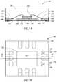
- FIG. 1Ais a cross-section view of a semiconductor package in accordance with one embodiment.
- FIG. 1Bis a bottom plan view of the semiconductor package of FIG. 1A .
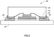
- FIG. 2is a cross-section view of the semiconductor package of FIG. 1A attached to a printed circuit board.
- FIGS. 3A-3Eare cross-section views of various stages of assembly of semiconductor packages in accordance with one embodiment.
- FIG. 1Ashows a cross-sectional view of a QFN leadframe package 100 in accordance with one embodiment of the disclosure.
- FIG. 1Bis a bottom plan view of the package 100 .
- the package 100includes a die pad 102 having inner and outer surfaces 104 , 106 .
- the package 100further includes a plurality of leads 110 , each having inner, bottom, and lateral surfaces 112 , 114 , 116 .
- the die pad 102 and the leads 110are formed from a leadframe, which is made of conductive material, typically copper or a copper alloy.
- the leads 110are located around the die pad 102 and form a recess at the corners of the package 100 where side surfaces of the package 100 meet with a bottom surface of the package 100 . Due to the recess, first portions of the leads 110 proximate the lateral surface 116 of the leads 110 have first thicknesses, while second portions of the leads 110 proximate the bottom surface 114 of the leads 110 have second, different thicknesses. The first thicknesses of the first portions of the leads are less than the second thicknesses of the second portions of the leads, thereby forming the recesses.
- the bottom surfaces 114 of the leads 110may be referred to as lands of the package and are configured to electrically couple the package 100 to another device or board, such as a PCB.
- the package 100includes three leads 110 on each side of the package 100 . It is to be appreciated, however, that any number of leads may be located on any number of sides of the die pad, including only one lead located on one side of the package.
- the semiconductor die 120is made from a semiconductor material, such as silicon, and includes an active surface in which integrated circuits are formed.
- the integrated circuitsmay be analog or digital circuits implemented as active devices, passive devices, conductive layers, and dielectric layers formed within the semiconductor die 120 and electrically interconnected according to the electrical design and function of the semiconductor die.
- the adhesive materialmay be any material configured to secure the semiconductor die 120 to the die pad 102 , such as glue, paste, tape, and the like.
- Conductive wires 122electrically couple the semiconductor die 120 to the leads 110 .
- a first end 124 of the conductive wire 122is coupled to a bond pad of the semiconductor die 120 and a second end 126 of the conductive wire 122 is coupled to the lead 110 .
- the semiconductor die 120may be flip chip coupled to the leads 110 , as is well known in the art.
- the semiconductor die 120is mechanically supported by the leads 110 and electrically coupled directly to the leads 110 by solder balls.
- the packagemay not include a die pad.
- Encapsulation material 130is located over the die pad 102 and the leads 110 covering the semiconductor die 120 and the conductive wires 122 to form a package body.
- the encapsulation material 130is also located between the leads 110 and the die pad 102 and forms a bottom surface of the package along with the outer surface 106 of the die pad 102 and the bottom surfaces 114 of the leads 110 . Furthermore, the encapsulation material 130 fills the recesses of the leads 110 at the bottom edges of the package 100 .
- the encapsulation material 130is an insulative material that protects the electrical components and materials from damage, such as corrosion, physical damage, moisture damage, or other causes of damage to electrical devices and materials.
- the encapsulation materialis a plastic material, such as a polymer resin.
- the bottom surfaces 114 of leads 110 and the outer surface 106 of die pad 102may include plated conductive layers 132 .
- the plated conductive layers 132may be a nanolayer or a microlayer of one or more conductive materials.
- plated conductive layeris one or more metal materials, such as Ni/Pd/Ag, Ni/Pd/Au—Ag alloy, or Ni/Pd/Au/Ag.
- the plated conductive layers 132are made from materials that prevent the leadframe from oxidizing.
- the inner surfaces 112 of the leads 110 and inner surface 104 of the die pad 102may include plated conductive layers as well.
- Wettable conductive layers 140are located at the corners of the package 100 over the encapsulation material 130 and exposed surfaces of the leads 110 , such as the bottom surfaces 114 and the lateral surfaces 116 .
- each of the wettable conductive layers 140covers portions of the lateral and bottom surfaces 116 , 114 of the leads 110 and the encapsulation material 130 therebetween.
- the wettable conductive layers 140cover the entire lateral surfaces 116 and/or bottom surfaces 114 of the leads 110 .
- the wettable conductive layers 140extend beyond the lateral surfaces 116 of the leads 110 onto the encapsulation material 130 above the lead 110 to provide a larger surface area for joining material, such as solder, to wick up, as will be explained below.
- the wettable conductive layers 140may be a nanolayer or a microlayer of one or more conductive materials.
- the wettable conductive layers 140are made of any conductive material that provides a wettable surface for a joining material, such as solder, used during surface mounting of the package 100 to another device or board. More particularly, the wettable conductive layers 140 enable solder to flow up the wettable conductive layers 140 on the side surface of package 100 , thereby improving the solder joint between the package 100 and the board.
- the wettable conductive layers 140are formed from one or more metal materials, such as gold, platinum, silver, nickel, or aluminum.
- the dimensions, such as the thickness, of the wettable conductive layer 140may be any dimension suitable for providing a wettable surface for the solder.
- the thickness of the wettable conductive layer 140is between 1.5 microns to 4 microns. However, it is to be appreciated that greater thicknesses, such as between 4 and 10 microns, may be used.
- the width of the wettable conductive layer 140may be substantially the same width as the leads 110 as in shown in FIG. 1B or may be greater or less than the width of the leads 110 .
- FIG. 2is a cross-section illustration of the package 100 of FIG. 1A coupled to a printed circuit board (PCB) 144 by solder joints 146 .
- PCBprinted circuit board
- FIG. 2is a cross-section illustration of the package 100 of FIG. 1A coupled to a printed circuit board (PCB) 144 by solder joints 146 .
- PCB 144includes one or more layers of insulative and conductive materials, as is well known in the art.
- the wettable conductive layers 140are wettable flanks for the joining material, such as solder, of the solder joints 146 to wick up the side of the package 100 when the package 100 is mounted to PCB 144 .
- FIG. 2illustrates that solder of the solder joints 146 has wicked up the side of the wettable conductive layers 140 located on the lateral surface 116 of the leads 110 and the encapsulation material 130 . With a portion of the solder joint 146 adhering to the package 100 at its side surface, a visual inspection of the solder joint 146 between the package 100 and the PCB 144 is thereby readily enabled.
- FIGS. 3A-3Eare cross-section views of various stages of assembly of semiconductor packages, such as the semiconductor package 100 of FIGS. 1A and 1B , in accordance with one embodiment.
- semiconductor dice 120are coupled to die pads 102 of a leadframe strip or array.
- the leadframe strip or arrayincludes connecting bars that couple the various components, such as the leads 110 and the die pads 102 , of the leadframe strip or array together.
- the leadframe strip or arraymay include pre-plated conductive layers 132 on the leads 110 and the die pads 102 of the leadframe strip.
- the semiconductor dice 120may be coupled by placing adhesive material, such as glue, paste, or tape, on one or both of the semiconductor dice 120 and the die pads 102 and coupling the semiconductor dice 120 to the die pads 102 . Furthermore, the semiconductor dice 120 are electrically coupled to the leads 110 by coupling first ends 124 of conductive wires 122 to bond pads of the semiconductor dice 120 and second ends 126 of the conductive wires 122 are coupled to the leads 110 .
- adhesive materialsuch as glue, paste, or tape
- encapsulation material 130is formed around the semiconductor dice 120 and conductive wires 122 and over the leads 110 and die pads 102 .
- the encapsulation material 130is formed by conventional techniques, which may be a molding process.
- the molding processmay include injecting a molding material, such as a resin molding compound, into a mold.
- the molding materialis hardened, which may involve a curing step.
- the encapsulation material 130may be placed on a flexible substrate, such as tape 150 .
- the packagesare singulated into individual packages 100 .
- the packages 100are singulated by cutting through the encapsulation material 130 between adjacent leads 110 as indicated by the arrows.
- the first portions of the leads 110are also cut to ensure that the lateral surfaces 116 of the leads 110 are exposed from the encapsulation material 130 at side surfaces of the package 100 .
- the singulationdoes not extend through the tape 150 .
- the singulation processmay include any suitable techniques, such as sawing or laser cutting, for separating the packages into individual packages.
- a saw blade used to cut through the encapsulation material 130 and leads 110will have a width that is greater than the width of the encapsulation material 130 between adjacent leads 110 of adjacent packages to ensure that first portions of the leads 110 are also cut to expose the lateral surfaces 116 of the leads 110 .
- the singulation processmay be improved.
- cutting through encapsulation material 130is substantially easier than cutting through the leadframe material, which as mentioned above is typically copper or a copper alloy.
- the blade life of the sawing processmay be lengthened.
- the throughput through the sawsis also improved in that the sawing speed may be increased.
- saw burrsmay be reduced or eliminated.
- saw burrscan form that extend beyond the bottom surface of the package.
- the saw burrs that extend beyond the bottom of the packagecan cause difficulties during surface mount, creating voids in the solder joints.
- saw bursare substantially eliminated or significantly reduced.
- the singulation processmay be more efficient and less costly than in the prior art.
- the tape 150may be stretched to further separate the individual packages 100 apart from each other as indicated by the arrows.
- the wettable conductive layers 140are formed on the packages 100 .
- the wettable conductive layers 140are printed on the side and bottom surfaces of the packages 100 . More particularly, the wettable conductive layers 140 are printed on the lateral surfaces 116 of the leads 110 , the bottom surfaces 114 of the leads 110 , and the encapsulation material 130 between the lateral surfaces 116 and bottom surfaces 114 of the leads 110 .
- the wettable conductive layers 140extend beyond lateral surfaces 116 of the leads 110 onto the encapsulation material 130 above the lateral surface 116 of the leads 110 . This provides a greater wettable surface area than is provided by lateral surfaces 116 of the leads 110 .
- the wettable conductive layers 140provide a wettable surface for solder to wick up during surface mount of the package 100 to another device or board.
- the wettable conductive layers 140are printed by ink printing technology, such as Aerosol Jet® technology, which is a maskless and contactless direct printing technology that can produce features with small dimensions. Aerosol Jet® technology allows for precisely deposited conductive materials with small dimensions. Generally described, Aerosol Jet® technology involves a conductive ink that is atomized. Aerosol and the atomized ink are provided to an impactor. In the impactor, the ink is densified and provided to a printing nozzle to print onto one or more surfaces. The conductive ink is printed through a nozzle onto package 100 to form the wettable conductive layer 140 .
- Aerosol Jet® technologyis a maskless and contactless direct printing technology that can produce features with small dimensions. Aerosol Jet® technology allows for precisely deposited conductive materials with small dimensions.
- Aerosol Jet® technologyinvolves a conductive ink that is atomized. Aerosol and the atomized ink are provided to an impactor. In the impactor, the ink is densified and provided to a printing nozzle to
- the conductive inkmay be printed at the edge of the package in a single printing step such that the conductive ink is printed on the side surface of the package and the bottom surface of the package in the same step.
- the printed conductive inkforms the wettable conductive layers 140 described above.
- the package 100is complete and may be removed from the tape 150 for mounting to another device or PCB as shown in FIG. 2 .
Landscapes
- Engineering & Computer Science (AREA)
- Physics & Mathematics (AREA)
- Microelectronics & Electronic Packaging (AREA)
- Condensed Matter Physics & Semiconductors (AREA)
- General Physics & Mathematics (AREA)
- Computer Hardware Design (AREA)
- Power Engineering (AREA)
- Manufacturing & Machinery (AREA)
- Geometry (AREA)
- Lead Frames For Integrated Circuits (AREA)
Abstract
Description
- Embodiments of the present disclosure are directed to leadless packages and methods of assembling same.
- Flat no-lead packages, such as quad flat no-lead (QFN) packages, are often utilized in applications in which small sized packages are desired. In general, flat no-lead packages provide a near chip scale encapsulated package that includes a planar leadframe. Lands (also referred to as leads) located on a bottom surface of the package and, in many cases, side surfaces of the package provide electrical connection to another device or board, such as a printed circuit board (PCB). In particular, the packages are mounted directly on the surface of the PCB using surface mount technology (SMT).
- Although no-lead packages that are mounted using SMT allow for smaller packages, it also creates some disadvantages. In particular, the solder joints between the package and the PCB can be weakened due to the PCB and the package having different coefficients of thermal expansions (CTE). Thus, the reliability of the package may in some cases depend on the integrity of the solder joints.
- As packages reduce in size, the available space for solder joints is further limited. Thus, strong solder bonds between the lands of the package and the pads of the board are desired. Furthermore, some applications specify a desire for visual inspection of the solder joints.
- Embodiments of the present disclosure are directed to flat no-lead packages with wettable sidewalls or flanks. In particular, wettable conductive layers are formed on the package over lateral portions of the leads and on portions of the package body, which may be encapsulation material. The wettable conductive layers may also be formed on bottom surfaces of the package body and the leads. The wettable conductive layers provide a wettable flank for solder to wick up when the package is mounted to a substrate, such as a PCB, using SMT. In particular, solder that is used to join the PCB and the package wicks up the side of the wettable conductive layers along a side surface of the package. In that regard, the solder is exposed and coupled to the side surface of the package at the wettable conductive layers, thereby allowing for a visual inspection of the solder joints. In various embodiments, the wettable conductive layers are formed on the package after the package body has been formed. In one embodiment, the wettable conductive layers are printed on the package body and the leads by Aerosol Jet® technology.
FIG. 1A is a cross-section view of a semiconductor package in accordance with one embodiment.FIG. 1B is a bottom plan view of the semiconductor package ofFIG. 1A .FIG. 2 is a cross-section view of the semiconductor package ofFIG. 1A attached to a printed circuit board.FIGS. 3A-3E are cross-section views of various stages of assembly of semiconductor packages in accordance with one embodiment.FIG. 1A shows a cross-sectional view of aQFN leadframe package 100 in accordance with one embodiment of the disclosure.FIG. 1B is a bottom plan view of thepackage 100. Thepackage 100 includes adie pad 102 having inner andouter surfaces package 100 further includes a plurality ofleads 110, each having inner, bottom, andlateral surfaces die pad 102 and theleads 110 are formed from a leadframe, which is made of conductive material, typically copper or a copper alloy.- The
leads 110 are located around thedie pad 102 and form a recess at the corners of thepackage 100 where side surfaces of thepackage 100 meet with a bottom surface of thepackage 100. Due to the recess, first portions of theleads 110 proximate thelateral surface 116 of theleads 110 have first thicknesses, while second portions of theleads 110 proximate thebottom surface 114 of theleads 110 have second, different thicknesses. The first thicknesses of the first portions of the leads are less than the second thicknesses of the second portions of the leads, thereby forming the recesses. Thebottom surfaces 114 of theleads 110 may be referred to as lands of the package and are configured to electrically couple thepackage 100 to another device or board, such as a PCB. - As shown in
FIG. 1B , thepackage 100 includes threeleads 110 on each side of thepackage 100. It is to be appreciated, however, that any number of leads may be located on any number of sides of the die pad, including only one lead located on one side of the package. - A
semiconductor die 120 that includes one or more electrical components, such as integrated circuits, is secured to theinner surface 104 of thedie pad 102 by an adhesive material (not shown). Thesemiconductor die 120 is made from a semiconductor material, such as silicon, and includes an active surface in which integrated circuits are formed. The integrated circuits may be analog or digital circuits implemented as active devices, passive devices, conductive layers, and dielectric layers formed within thesemiconductor die 120 and electrically interconnected according to the electrical design and function of the semiconductor die. The adhesive material may be any material configured to secure thesemiconductor die 120 to thedie pad 102, such as glue, paste, tape, and the like. Conductive wires 122 electrically couple the semiconductor die120 to theleads 110. For instance, afirst end 124 of theconductive wire 122 is coupled to a bond pad of the semiconductor die120 and asecond end 126 of theconductive wire 122 is coupled to thelead 110. Although not shown, it will be understood to persons of ordinary skill in the art that in another embodiment, thesemiconductor die 120 may be flip chip coupled to theleads 110, as is well known in the art. In that regard, thesemiconductor die 120 is mechanically supported by theleads 110 and electrically coupled directly to theleads 110 by solder balls. Thus, in such an embodiment, the package may not include a die pad.Encapsulation material 130 is located over thedie pad 102 and theleads 110 covering the semiconductor die120 and theconductive wires 122 to form a package body. Theencapsulation material 130 is also located between theleads 110 and thedie pad 102 and forms a bottom surface of the package along with theouter surface 106 of thedie pad 102 and thebottom surfaces 114 of theleads 110. Furthermore, theencapsulation material 130 fills the recesses of theleads 110 at the bottom edges of thepackage 100. Theencapsulation material 130 is an insulative material that protects the electrical components and materials from damage, such as corrosion, physical damage, moisture damage, or other causes of damage to electrical devices and materials. In one embodiment, the encapsulation material is a plastic material, such as a polymer resin.- The
bottom surfaces 114 ofleads 110 and theouter surface 106 of diepad 102 may include platedconductive layers 132. The platedconductive layers 132 may be a nanolayer or a microlayer of one or more conductive materials. For instance, plated conductive layer is one or more metal materials, such as Ni/Pd/Ag, Ni/Pd/Au—Ag alloy, or Ni/Pd/Au/Ag. The platedconductive layers 132 are made from materials that prevent the leadframe from oxidizing. Although not shown, theinner surfaces 112 of theleads 110 andinner surface 104 of thedie pad 102 may include plated conductive layers as well. - Wettable
conductive layers 140 are located at the corners of thepackage 100 over theencapsulation material 130 and exposed surfaces of theleads 110, such as the bottom surfaces114 and the lateral surfaces116. In particular, each of the wettableconductive layers 140 covers portions of the lateral andbottom surfaces leads 110 and theencapsulation material 130 therebetween. In one embodiment, the wettableconductive layers 140 cover the entire lateral surfaces116 and/orbottom surfaces 114 of theleads 110. In the illustrative embodiment, the wettableconductive layers 140 extend beyond thelateral surfaces 116 of theleads 110 onto theencapsulation material 130 above thelead 110 to provide a larger surface area for joining material, such as solder, to wick up, as will be explained below. - The wettable
conductive layers 140 may be a nanolayer or a microlayer of one or more conductive materials. In particular, the wettableconductive layers 140 are made of any conductive material that provides a wettable surface for a joining material, such as solder, used during surface mounting of thepackage 100 to another device or board. More particularly, the wettableconductive layers 140 enable solder to flow up the wettableconductive layers 140 on the side surface ofpackage 100, thereby improving the solder joint between thepackage 100 and the board. In one embodiment, the wettableconductive layers 140 are formed from one or more metal materials, such as gold, platinum, silver, nickel, or aluminum. - The dimensions, such as the thickness, of the wettable
conductive layer 140 may be any dimension suitable for providing a wettable surface for the solder. In one embodiment, the thickness of the wettableconductive layer 140 is between 1.5 microns to 4 microns. However, it is to be appreciated that greater thicknesses, such as between 4 and 10 microns, may be used. The width of the wettableconductive layer 140 may be substantially the same width as theleads 110 as in shown inFIG. 1B or may be greater or less than the width of theleads 110. FIG. 2 is a cross-section illustration of thepackage 100 ofFIG. 1A coupled to a printed circuit board (PCB)144 bysolder joints 146. Although the details are of thePCB 144 are not shown, it will be understood that thePCB 144 includes one or more layers of insulative and conductive materials, as is well known in the art.- As shown in
FIG. 2 , the wettableconductive layers 140 are wettable flanks for the joining material, such as solder, of the solder joints146 to wick up the side of thepackage 100 when thepackage 100 is mounted toPCB 144. In particular,FIG. 2 illustrates that solder of the solder joints146 has wicked up the side of the wettableconductive layers 140 located on thelateral surface 116 of theleads 110 and theencapsulation material 130. With a portion of the solder joint146 adhering to thepackage 100 at its side surface, a visual inspection of the solder joint146 between thepackage 100 and thePCB 144 is thereby readily enabled. That is, due to the wettableconductive layer 140 being higher on the side of package and thus farther from thePCB 144, an inspector has more surface area along the side surface of thepackage 100 to inspect thesolder joint 146. Thus, not only is the surface area for joining thepackage 100 to thePCB 144 greater thereby increasing the mechanical and electrical connection between theleads 110 and thePCB 144, but also a visual inspection of the solder joint146 may be more easily completed than over the prior art. FIGS. 3A-3E are cross-section views of various stages of assembly of semiconductor packages, such as thesemiconductor package 100 ofFIGS. 1A and 1B , in accordance with one embodiment.- As shown in
FIG. 3A ,semiconductor dice 120 are coupled to diepads 102 of a leadframe strip or array. Although not shown, the leadframe strip or array includes connecting bars that couple the various components, such as theleads 110 and thedie pads 102, of the leadframe strip or array together. The leadframe strip or array may include pre-platedconductive layers 132 on theleads 110 and thedie pads 102 of the leadframe strip. - The
semiconductor dice 120 may be coupled by placing adhesive material, such as glue, paste, or tape, on one or both of thesemiconductor dice 120 and thedie pads 102 and coupling thesemiconductor dice 120 to thedie pads 102. Furthermore, thesemiconductor dice 120 are electrically coupled to theleads 110 by coupling first ends124 ofconductive wires 122 to bond pads of thesemiconductor dice 120 and second ends126 of theconductive wires 122 are coupled to theleads 110. - As shown in
FIG. 3B ,encapsulation material 130 is formed around thesemiconductor dice 120 andconductive wires 122 and over theleads 110 and diepads 102. Theencapsulation material 130 is formed by conventional techniques, which may be a molding process. For instance, the molding process may include injecting a molding material, such as a resin molding compound, into a mold. The molding material is hardened, which may involve a curing step. Upon hardening theencapsulation material 130, theencapsulation material 130 may be placed on a flexible substrate, such astape 150. - As shown in
FIG. 3C , after theencapsulation material 130 has been placed on thetape 150, the packages are singulated intoindividual packages 100. In particular, thepackages 100 are singulated by cutting through theencapsulation material 130 betweenadjacent leads 110 as indicated by the arrows. The first portions of theleads 110 are also cut to ensure that thelateral surfaces 116 of theleads 110 are exposed from theencapsulation material 130 at side surfaces of thepackage 100. The singulation does not extend through thetape 150. - The singulation process may include any suitable techniques, such as sawing or laser cutting, for separating the packages into individual packages. In a sawing process, a saw blade used to cut through the
encapsulation material 130 and leads110 will have a width that is greater than the width of theencapsulation material 130 betweenadjacent leads 110 of adjacent packages to ensure that first portions of theleads 110 are also cut to expose thelateral surfaces 116 of theleads 110. - It is to be appreciated that by having
encapsulation material 130 surrounding the first portions (the thinner portions) of theleads 110, the singulation process may be improved. First of all, cutting throughencapsulation material 130 is substantially easier than cutting through the leadframe material, which as mentioned above is typically copper or a copper alloy. Thus, by cutting through smaller thicknesses of first portions of theleads 110, rather than the larger thicknesses of the second portions of theleads 110, the blade life of the sawing process may be lengthened. Additionally, the throughput through the saws is also improved in that the sawing speed may be increased. - Furthermore, by not cutting through leads that extend to the corner edge of the package, saw burrs may be reduced or eliminated. Typically, when sawing through leads that extend to the corner edge of the package, saw burrs can form that extend beyond the bottom surface of the package. The saw burrs that extend beyond the bottom of the package can cause difficulties during surface mount, creating voids in the solder joints. By cutting through encapsulation material on both sides of the leads, saw burs are substantially eliminated or significantly reduced. Thus, the singulation process may be more efficient and less costly than in the prior art.
- As shown in
FIG. 3D , thetape 150 may be stretched to further separate theindividual packages 100 apart from each other as indicated by the arrows. - As shown in
FIG. 3E , the wettableconductive layers 140 are formed on thepackages 100. In particular, the wettableconductive layers 140 are printed on the side and bottom surfaces of thepackages 100. More particularly, the wettableconductive layers 140 are printed on the lateral surfaces116 of theleads 110, the bottom surfaces114 of theleads 110, and theencapsulation material 130 between thelateral surfaces 116 andbottom surfaces 114 of theleads 110. In the illustrated embodiment, the wettableconductive layers 140 extend beyondlateral surfaces 116 of theleads 110 onto theencapsulation material 130 above thelateral surface 116 of theleads 110. This provides a greater wettable surface area than is provided bylateral surfaces 116 of theleads 110. As mentioned above, the wettableconductive layers 140 provide a wettable surface for solder to wick up during surface mount of thepackage 100 to another device or board. - The wettable
conductive layers 140 are printed by ink printing technology, such as Aerosol Jet® technology, which is a maskless and contactless direct printing technology that can produce features with small dimensions. Aerosol Jet® technology allows for precisely deposited conductive materials with small dimensions. Generally described, Aerosol Jet® technology involves a conductive ink that is atomized. Aerosol and the atomized ink are provided to an impactor. In the impactor, the ink is densified and provided to a printing nozzle to print onto one or more surfaces. The conductive ink is printed through a nozzle ontopackage 100 to form the wettableconductive layer 140. The conductive ink may be printed at the edge of the package in a single printing step such that the conductive ink is printed on the side surface of the package and the bottom surface of the package in the same step. The printed conductive ink forms the wettableconductive layers 140 described above. After printing the conductive ink, thepackage 100 is complete and may be removed from thetape 150 for mounting to another device or PCB as shown inFIG. 2 . - The various embodiments described above can be combined to provide further embodiments. All of the U.S. patents, U.S. patent application publications, U.S. patent applications, foreign patents, foreign patent applications and non-patent publications referred to in this specification and/or listed in the Application Data Sheet are incorporated herein by reference, in their entirety. Aspects of the embodiments can be modified, if necessary to employ concepts of the various patents, applications and publications to provide yet further embodiments.
- These and other changes can be made to the embodiments in light of the above-detailed description. In general, in the following claims, the terms used should not be construed to limit the claims to the specific embodiments disclosed in the specification and the claims, but should be construed to include all possible embodiments along with the full scope of equivalents to which such claims are entitled. Accordingly, the claims are not limited by the disclosure.
Claims (20)
Priority Applications (1)
| Application Number | Priority Date | Filing Date | Title |
|---|---|---|---|
| US17/155,520US20210143089A1 (en) | 2016-05-19 | 2021-01-22 | Semiconductor package with wettable flank |
Applications Claiming Priority (2)
| Application Number | Priority Date | Filing Date | Title |
|---|---|---|---|
| US15/159,604US10930581B2 (en) | 2016-05-19 | 2016-05-19 | Semiconductor package with wettable flank |
| US17/155,520US20210143089A1 (en) | 2016-05-19 | 2021-01-22 | Semiconductor package with wettable flank |
Related Parent Applications (1)
| Application Number | Title | Priority Date | Filing Date |
|---|---|---|---|
| US15/159,604DivisionUS10930581B2 (en) | 2016-05-19 | 2016-05-19 | Semiconductor package with wettable flank |
Publications (1)
| Publication Number | Publication Date |
|---|---|
| US20210143089A1true US20210143089A1 (en) | 2021-05-13 |
Family
ID=59028808
Family Applications (2)
| Application Number | Title | Priority Date | Filing Date |
|---|---|---|---|
| US15/159,604Active2038-06-24US10930581B2 (en) | 2016-05-19 | 2016-05-19 | Semiconductor package with wettable flank |
| US17/155,520PendingUS20210143089A1 (en) | 2016-05-19 | 2021-01-22 | Semiconductor package with wettable flank |
Family Applications Before (1)
| Application Number | Title | Priority Date | Filing Date |
|---|---|---|---|
| US15/159,604Active2038-06-24US10930581B2 (en) | 2016-05-19 | 2016-05-19 | Semiconductor package with wettable flank |
Country Status (2)
| Country | Link |
|---|---|
| US (2) | US10930581B2 (en) |
| CN (2) | CN206259346U (en) |
Families Citing this family (24)
| Publication number | Priority date | Publication date | Assignee | Title |
|---|---|---|---|---|
| US10930581B2 (en)* | 2016-05-19 | 2021-02-23 | Stmicroelectronics S.R.L. | Semiconductor package with wettable flank |
| US10121742B2 (en)* | 2017-03-15 | 2018-11-06 | Amkor Technology, Inc. | Method of forming a packaged semiconductor device using ganged conductive connective assembly and structure |
| US10199312B1 (en)* | 2017-09-09 | 2019-02-05 | Amkor Technology, Inc. | Method of forming a packaged semiconductor device having enhanced wettable flank and structure |
| DE102017129924B4 (en)* | 2017-12-14 | 2021-04-29 | Infineon Technologies Ag | ENCAPSULATED, TERMINAL LESS PACKAGE WITH AT LEAST PARTIALLY EXPOSED INSIDE WALL OF A CHIP CARRIER, ELECTRONIC DEVICE, METHOD FOR MANUFACTURING A PACKAGE WITHOUT TERMINAL LADIES AND PREPARING METHOD FOR ESTABLISHING A PACKAGE |
| US11069601B2 (en)* | 2018-02-27 | 2021-07-20 | Stmicroelectronics, Inc. | Leadless semiconductor package with wettable flanks |
| JP7051508B2 (en)* | 2018-03-16 | 2022-04-11 | ローム株式会社 | Semiconductor devices and methods for manufacturing semiconductor devices |
| US11495524B2 (en)* | 2018-06-12 | 2022-11-08 | Texas Instruments Incorporated | QFN device having a mechanism that enables an inspectable solder joint when attached to a PWB and method of making same |
| US20200227343A1 (en)* | 2019-01-11 | 2020-07-16 | Chang Wah Technology Co., Ltd. | Semiconductor device package |
| JP7384918B2 (en) | 2019-03-08 | 2023-11-21 | シリコニックス インコーポレイテッド | Semiconductor package with sidewall plating layer |
| CN113614893A (en) | 2019-03-08 | 2021-11-05 | 硅尼克斯公司 | Semiconductor package with side wall coating |
| US12211774B2 (en)* | 2019-04-25 | 2025-01-28 | Stmicroelectronics, Inc. | Lead stabilization in semiconductor packages |
| CN112151463A (en)* | 2019-06-28 | 2020-12-29 | 意法半导体公司 | Semiconductor package with cavity in die pad for reducing voids in solder |
| US11437526B2 (en)* | 2019-12-09 | 2022-09-06 | Amkor Technology Singapore Holding Pte. Ltd. | Electronic devices having a sensor and a translucent mold compound and methods of manufacturing electronic devices |
| CN113035722A (en) | 2019-12-24 | 2021-06-25 | 维谢综合半导体有限责任公司 | Packaging process for plating with selective molding |
| CN113035721A (en)* | 2019-12-24 | 2021-06-25 | 维谢综合半导体有限责任公司 | Packaging process for plating conductive film on side wall |
| US11462484B2 (en)* | 2020-10-08 | 2022-10-04 | Advanced Semiconductor Engineering, Inc. | Electronic package with wettable flank and shielding layer and manufacturing method thereof |
| US20220139845A1 (en)* | 2020-10-30 | 2022-05-05 | Stmicroelectronics, Inc. | Semiconductor package with electromagnetic shield |
| DE102021129753A1 (en)* | 2020-12-17 | 2022-06-23 | Infineon Technologies Ag | Semiconductor packages and methods of making the same |
| JP7621130B2 (en)* | 2021-02-09 | 2025-01-24 | エイブリック株式会社 | Semiconductor Device |
| CN113555326A (en)* | 2021-06-03 | 2021-10-26 | 珠海越亚半导体股份有限公司 | Packaging structure capable of wetting side face, manufacturing method thereof and vertical packaging module |
| KR20230046097A (en) | 2021-09-29 | 2023-04-05 | 해성디에스 주식회사 | Lead frame |
| US20230114872A1 (en)* | 2021-10-13 | 2023-04-13 | Texas Instruments Incorporated | Electronic device with wettable flank lead |
| CN116387198B (en)* | 2023-04-07 | 2024-11-01 | 上海聚跃检测技术有限公司 | Cutting and separating method for QFN (quad Flat No-lead) packaged chips |
| US20250046621A1 (en)* | 2023-07-31 | 2025-02-06 | Texas Instruments Incorporated | Ic package with immersion tin on flank |
Citations (9)
| Publication number | Priority date | Publication date | Assignee | Title |
|---|---|---|---|---|
| US6489218B1 (en)* | 2001-06-21 | 2002-12-03 | Advanced Semiconductor Engineering, Inc. | Singulation method used in leadless packaging process |
| US20030049884A1 (en)* | 2001-09-12 | 2003-03-13 | Lutz Michael A. | Apparatus with compliant electrical terminals, and methods for forming same |
| US20060082021A1 (en)* | 2001-10-10 | 2006-04-20 | Williams Vernon M | Leadframe and method for reducing mold compound adhesion problems |
| US20060199308A1 (en)* | 2005-03-02 | 2006-09-07 | Advanced Semiconductor Engineering, Inc. | Process for manufacturing sawing type leadless semiconductor packages |
| US20070117259A1 (en)* | 2005-11-18 | 2007-05-24 | Semiconductor Components Industries, Llc. | Semiconductor component and method of manufacture |
| WO2009125250A1 (en)* | 2008-04-11 | 2009-10-15 | Freescale Semiconductor, Inc. | Integrated circuit package, method of manufacturing an integrated circuit package and printed circuit board |
| US20100159630A1 (en)* | 2008-12-18 | 2010-06-24 | Twin Creeks Technologies, Inc. | Method for making a photovoltaic cell comprising contact regions doped through a lamina |
| US20120049335A1 (en)* | 2010-08-31 | 2012-03-01 | Utac Thai Limited | Singulation method for semiconductor package with plating on side of connectors |
| US20150147848A1 (en)* | 2012-09-24 | 2015-05-28 | Seiko Instruments Inc. | Resin-encapsulated semiconductor device and method of manufacturing the same |
Family Cites Families (14)
| Publication number | Priority date | Publication date | Assignee | Title |
|---|---|---|---|---|
| JP3062192B1 (en) | 1999-09-01 | 2000-07-10 | 松下電子工業株式会社 | Lead frame and method of manufacturing resin-encapsulated semiconductor device using the same |
| US7042068B2 (en) | 2000-04-27 | 2006-05-09 | Amkor Technology, Inc. | Leadframe and semiconductor package made using the leadframe |
| US6400004B1 (en)* | 2000-08-17 | 2002-06-04 | Advanced Semiconductor Engineering, Inc. | Leadless semiconductor package |
| TWI297938B (en) | 2003-07-15 | 2008-06-11 | Advanced Semiconductor Eng | Semiconductor package |
| JP2005244035A (en) | 2004-02-27 | 2005-09-08 | Renesas Technology Corp | Mounting method of semiconductor device, and semiconductor device |
| DE102005006995B4 (en) | 2005-02-15 | 2008-01-24 | Infineon Technologies Ag | Semiconductor device with plastic housing and external connections and method for producing the same |
| US8097497B2 (en) | 2007-03-30 | 2012-01-17 | Xerox Corporation | Inkjet printed wirebonds, encapsulant and shielding |
| US8163629B2 (en) | 2010-08-05 | 2012-04-24 | Infineon Technologies Ag | Metallization for chip scale packages in wafer level packaging |
| CN102789994B (en) | 2011-05-18 | 2016-08-10 | 飞思卡尔半导体公司 | The wettable semiconductor device in side |
| US9070669B2 (en) | 2012-11-09 | 2015-06-30 | Freescale Semiconductor, Inc. | Wettable lead ends on a flat-pack no-lead microelectronic package |
| US9305911B2 (en) | 2013-12-05 | 2016-04-05 | Freescale Semiconductor, Inc. | Devices and stacked microelectronic packages with package surface conductors and adjacent trenches and methods of their fabrication |
| CN105206596B (en) | 2014-06-06 | 2018-12-07 | 恩智浦美国有限公司 | Packaging integrated circuit devices with bending lead |
| JP6840466B2 (en)* | 2016-03-08 | 2021-03-10 | 株式会社アムコー・テクノロジー・ジャパン | Semiconductor package and manufacturing method of semiconductor package |
| US10930581B2 (en)* | 2016-05-19 | 2021-02-23 | Stmicroelectronics S.R.L. | Semiconductor package with wettable flank |
- 2016
- 2016-05-19USUS15/159,604patent/US10930581B2/enactiveActive
- 2016-12-12CNCN201621356215.8Upatent/CN206259346U/enactiveActive
- 2016-12-12CNCN201611138076.6Apatent/CN107403765A/enactivePending
- 2021
- 2021-01-22USUS17/155,520patent/US20210143089A1/enactivePending
Patent Citations (9)
| Publication number | Priority date | Publication date | Assignee | Title |
|---|---|---|---|---|
| US6489218B1 (en)* | 2001-06-21 | 2002-12-03 | Advanced Semiconductor Engineering, Inc. | Singulation method used in leadless packaging process |
| US20030049884A1 (en)* | 2001-09-12 | 2003-03-13 | Lutz Michael A. | Apparatus with compliant electrical terminals, and methods for forming same |
| US20060082021A1 (en)* | 2001-10-10 | 2006-04-20 | Williams Vernon M | Leadframe and method for reducing mold compound adhesion problems |
| US20060199308A1 (en)* | 2005-03-02 | 2006-09-07 | Advanced Semiconductor Engineering, Inc. | Process for manufacturing sawing type leadless semiconductor packages |
| US20070117259A1 (en)* | 2005-11-18 | 2007-05-24 | Semiconductor Components Industries, Llc. | Semiconductor component and method of manufacture |
| WO2009125250A1 (en)* | 2008-04-11 | 2009-10-15 | Freescale Semiconductor, Inc. | Integrated circuit package, method of manufacturing an integrated circuit package and printed circuit board |
| US20100159630A1 (en)* | 2008-12-18 | 2010-06-24 | Twin Creeks Technologies, Inc. | Method for making a photovoltaic cell comprising contact regions doped through a lamina |
| US20120049335A1 (en)* | 2010-08-31 | 2012-03-01 | Utac Thai Limited | Singulation method for semiconductor package with plating on side of connectors |
| US20150147848A1 (en)* | 2012-09-24 | 2015-05-28 | Seiko Instruments Inc. | Resin-encapsulated semiconductor device and method of manufacturing the same |
Also Published As
| Publication number | Publication date |
|---|---|
| CN206259346U (en) | 2017-06-16 |
| US20170338170A1 (en) | 2017-11-23 |
| CN107403765A (en) | 2017-11-28 |
| US10930581B2 (en) | 2021-02-23 |
Similar Documents
| Publication | Publication Date | Title |
|---|---|---|
| US20210143089A1 (en) | Semiconductor package with wettable flank | |
| US12094725B2 (en) | Leadframe package with pre-applied filler material | |
| JP5689462B2 (en) | Semiconductor device and manufacturing method thereof | |
| JP5271949B2 (en) | Semiconductor device | |
| US7439097B2 (en) | Taped lead frames and methods of making and using the same in semiconductor packaging | |
| KR102227588B1 (en) | Semiconductor device and method of manufacturing the same | |
| US20150076675A1 (en) | Leadframe package with wettable sides and method of manufacturing same | |
| CN209785926U (en) | semiconductor device with a plurality of transistors | |
| WO2006109566A1 (en) | Semiconductor device | |
| CN106711113A (en) | Semiconductor package with integrated heatsink | |
| CN211125636U (en) | semiconductor package | |
| JP5946511B2 (en) | Manufacturing method of semiconductor device | |
| CN111863762A (en) | Lead stabilization in semiconductor packages | |
| JP2006165411A (en) | Semiconductor device and manufacturing method thereof | |
| JP2009200175A (en) | Semiconductor device and manufacturing method thereof | |
| JP2000286375A (en) | Semiconductor device | |
| JP4531073B2 (en) | Semiconductor device | |
| JP2000286372A (en) | Manufacture of semiconductor device | |
| JP2008108967A (en) | Lead frame and method for manufacturing semiconductor package using it | |
| JP2003338589A (en) | BGA package and manufacturing method thereof | |
| KR20030045224A (en) | A chip scale package manufactured by wire bonding method and a manufacturing method thereof |
Legal Events
| Date | Code | Title | Description |
|---|---|---|---|
| STPP | Information on status: patent application and granting procedure in general | Free format text:APPLICATION DISPATCHED FROM PREEXAM, NOT YET DOCKETED | |
| STPP | Information on status: patent application and granting procedure in general | Free format text:DOCKETED NEW CASE - READY FOR EXAMINATION | |
| STPP | Information on status: patent application and granting procedure in general | Free format text:RESPONSE TO NON-FINAL OFFICE ACTION ENTERED AND FORWARDED TO EXAMINER | |
| STPP | Information on status: patent application and granting procedure in general | Free format text:FINAL REJECTION MAILED | |
| STPP | Information on status: patent application and granting procedure in general | Free format text:DOCKETED NEW CASE - READY FOR EXAMINATION | |
| STPP | Information on status: patent application and granting procedure in general | Free format text:NON FINAL ACTION MAILED | |
| STPP | Information on status: patent application and granting procedure in general | Free format text:RESPONSE TO NON-FINAL OFFICE ACTION ENTERED AND FORWARDED TO EXAMINER | |
| STPP | Information on status: patent application and granting procedure in general | Free format text:FINAL REJECTION MAILED | |
| STPP | Information on status: patent application and granting procedure in general | Free format text:RESPONSE AFTER FINAL ACTION FORWARDED TO EXAMINER | |
| STPP | Information on status: patent application and granting procedure in general | Free format text:ADVISORY ACTION MAILED | |
| STPP | Information on status: patent application and granting procedure in general | Free format text:DOCKETED NEW CASE - READY FOR EXAMINATION | |
| STPP | Information on status: patent application and granting procedure in general | Free format text:RESPONSE TO NON-FINAL OFFICE ACTION ENTERED AND FORWARDED TO EXAMINER | |
| STPP | Information on status: patent application and granting procedure in general | Free format text:ALLOWED -- NOTICE OF ALLOWANCE NOT YET MAILED Free format text:NOTICE OF ALLOWANCE MAILED -- APPLICATION RECEIVED IN OFFICE OF PUBLICATIONS |