US20210136266A1 - Image capturing device and appearance inspecting device including the same - Google Patents
Image capturing device and appearance inspecting device including the sameDownload PDFInfo
- Publication number
- US20210136266A1 US20210136266A1US17/074,694US202017074694AUS2021136266A1US 20210136266 A1US20210136266 A1US 20210136266A1US 202017074694 AUS202017074694 AUS 202017074694AUS 2021136266 A1US2021136266 A1US 2021136266A1
- Authority
- US
- United States
- Prior art keywords
- image
- appearance
- image capturing
- component
- light modules
- Prior art date
- Legal status (The legal status is an assumption and is not a legal conclusion. Google has not performed a legal analysis and makes no representation as to the accuracy of the status listed.)
- Granted
Links
- 239000003086colorantSubstances0.000claimsdescription5
- 230000007547defectEffects0.000description7
- 238000001514detection methodMethods0.000description7
- 238000010586diagramMethods0.000description5
- 230000008901benefitEffects0.000description2
- 238000007689inspectionMethods0.000description1
- 239000000463materialSubstances0.000description1
- 238000012986modificationMethods0.000description1
- 230000004048modificationEffects0.000description1
Images


Classifications
- H04N5/2256—
- G—PHYSICS
- G01—MEASURING; TESTING
- G01N—INVESTIGATING OR ANALYSING MATERIALS BY DETERMINING THEIR CHEMICAL OR PHYSICAL PROPERTIES
- G01N21/00—Investigating or analysing materials by the use of optical means, i.e. using sub-millimetre waves, infrared, visible or ultraviolet light
- G01N21/84—Systems specially adapted for particular applications
- G01N21/88—Investigating the presence of flaws or contamination
- G01N21/8806—Specially adapted optical and illumination features
- H—ELECTRICITY
- H04—ELECTRIC COMMUNICATION TECHNIQUE
- H04N—PICTORIAL COMMUNICATION, e.g. TELEVISION
- H04N23/00—Cameras or camera modules comprising electronic image sensors; Control thereof
- H04N23/56—Cameras or camera modules comprising electronic image sensors; Control thereof provided with illuminating means
- H—ELECTRICITY
- H04—ELECTRIC COMMUNICATION TECHNIQUE
- H04N—PICTORIAL COMMUNICATION, e.g. TELEVISION
- H04N23/00—Cameras or camera modules comprising electronic image sensors; Control thereof
- H04N23/50—Constructional details
- H04N5/2251—
Definitions
- the inventionrelates to an image capturing device.
- an image capturing deviceincludes an image capture component and N light modules.
- the image capture componentis configured to capture an appearance image of a component.
- the N light modulesare disposed around the image capture component, to be turned on alternately, and N 4. When at least one of the N light modules is turned on, the image capture component captures the appearance image of the component.
- an appearance inspecting deviceincludes at least two image capturing devices arranged side by side in one direction.
- Each of the image capturing devicesincludes an image capture component and N light modules.
- the image capture componentis configured to capture an appearance image of a component.
- the N light modulesare disposed around the image capture component, to be turned on alternately, and N 4. When at least one of the N light modules is turned on, the image capture component captures the appearance image of the component.
- the image capturing device and the appearance inspecting device including the same disclosed in this disclosureinclude a plurality of light modules and at least one image capturing element and provide a complete appearance image by alternately turning on a plurality of light modules and controlling the image capturing element to capture a plurality of appearance images.
- the image capturing device disclosed hereinprovides complete appearance images automatically, thus increases the efficiency of defect detection.
- FIG. 1is a three-dimensional schematic diagram of an image capturing device of an embodiment
- FIG. 2is a schematic circuit diagram of an appearance inspecting device of an embodiment
- FIG. 3is a schematic structural view of an appearance inspecting device having an image capturing device according to an embodiment
- FIG. 4is a schematic structural view of an appearance inspecting device during detection according to an embodiment
- FIG. 5is a three-dimensional schematic diagram of an image capturing device of an embodiment
- FIG. 6is a partial structural diagram of an appearance inspecting device of an embodiment
- FIG. 7is a partial structural diagram of an appearance inspecting device of an embodiment.
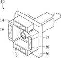
- An image capturing device 10includes an image capture component 12 and N light modules, wherein N 4 and is an even number.
- Nis equal to 4, that is, the four light modules 14 , 16 , 18 , and 20 are provided in the embodiment, which is not limited herein.
- the image capture component 12captures the appearance image of a component.
- the light modules 14 , 16 , 18 , and 20are arranged around the periphery of the image capture component 12 in a rectangle. Each of the light modules 14 , 16 , 18 , 20 produces a uniform light source.
- the image capture component 12captures the appearance image of the component 46 (as shown in FIG. 4 ).
- the image capture component 12cooperates with the light modules 14 , 16 , 18 , and 20 , to capture the appearance image of the testing area of the component when the light modules 14 , 16 , 18 , and 20 are turned on alternately.
- the image capturing device 10further includes a carrying plate 26 , and the image capture component 12 and the light modules 14 , 16 , 18 , and 20 around the image capture component 12 are all disposed on the surface of the carrying plate 26 .
- the image capture component 12is a camera or a video camera.
- the light modules 14 , 16 , 18 , 20include multiple light emitting diodes (LEDs) or light tubes.
- the image capture component 12 and the light modules 14 , 16 , 18 , 20are electrically connected to a processor 28 .
- the processor 28controls the light modules 14 , 16 , 18 , 20 to be turned on alternately and controls the image capture component 12 to capture the appearance image of the component respectively when the light modules 14 , 16 , 18 , and 20 are turned on alternately.
- the processor 28is a system on chip (SoC), a microcontroller (MCU), a central the processor (CPU), or a special application integrated circuit (ASIC).
- SoCsystem on chip
- MCUmicrocontroller
- CPUcentral the processor
- ASICspecial application integrated circuit
- the processor 28is a processor of a desktop, a laptop, a tablet, or a smartphone.
- the appearance inspecting device 40includes the image capturing device 10 , a double-axis moving mechanism 42 and a mobile platform 44 .
- the processor 28is electrically connected to the double-axis moving mechanism 42 and the mobile platform 44 , to control the double-axis moving mechanism 42 and the mobile platform 44 , respectively.
- the image capturing device 10is disposed on the double-axis moving mechanism 42 , and the double-axis moving mechanism 42 drives the image capturing device 10 to move left and right in a first direction (such as the X-axis direction) and to move up and down in a second direction (such as the Z-axis direction).
- the double-axis moving mechanism 42drives the image capturing device 10 to move up and down in the Z-axis direction
- the range of the component 46 covered by the light emitted from the light modules 14 , 16 , 18 , 20is adjustable by moving the image capturing device 10 up and down.
- the mobile platform 44is disposed under the image capturing device 10 .
- a component 46is placed on the mobile platform 44 , and the mobile platform 44 drives the component 46 to move back and forth in a third direction (such as the Y-axis direction). In this way, through the cooperation of the double-axis moving mechanism 42 and the mobile platform 44 , three-axis relative movement is performed to locate the image capturing device 10 above the component 46 for capturing image.
- the image capturing device 10is located above the testing area of the component 46 .
- the processor 28controls the light modules 14 , 16 , 18 , 20 to be turned on alternately and controls the image capture component 12 to respectively capture the appearance image of the testing area of the component when the light modules 14 , 16 , 18 , and 20 are turned on alternately.
- the image capture component 12captures the first appearance image when the processor 28 controls the light module 14 to illuminate the component 46 .
- the image capture component 12captures the second appearance image when the processor 28 controls the light module 16 to illuminate the component 46 .
- the image capture component 12captures the third appearance image when the processor 28 controls the light module 18 to illuminate the component 46 .
- the image capture component 12captures the fourth appearance image when the processor 28 controls the light module 20 to illuminate the component 46 .
- the image capture component 12captures at least N appearance images at the same position of the component 46 , and N is equal to 4 in this embodiment.
- the processor 28When capturing at least N pieces of the appearance image (that is, the first appearance image to the fourth appearance image), the processor 28 obtains at least N pixels corresponding to each pixel position from at least N pieces of the appearance image. In other words, the processor 28 respectively obtains a pixel at the same pixel position of the first appearance image to the fourth appearance image. As there are four appearance images, there are four pixels in the same pixel position. Then, the processor 28 obtains the best pixel color of each pixel position according to the at least N pixels and a calculation program to generate a final image.
- the processor 28first sorts the four pixels according to the brightness of the four pixels (such as from the brightest pixel to the darkest pixel), discards the darkest and brightest pixels, and takes the average of the colors (RGB) of the pixels with intermediate brightness as the best pixel color of the corresponding pixel position. Since the best pixel colors of all the pixel positions are obtained, a clear final image is also obtained. In this embodiment, since the final image is composed of the best pixel colors obtained from the four appearance images, the final image is actually a clear image. When there is a defect on the component 46 , the defect is clearly shown on the final image, so the appearance defect detection is completed based on the final image by the computer (the processor).
- the processor 28selectively controls the light modules 14 , 16 , 18 , 20 to emit light alternately.
- One or more of the light modules 14 , 16 , 18 , 20is selectively turned on alternately at each time, which is determined according to the actual testing needs.
- the light modules 14 , 16 , 18 , 20 of the image capturing device 10is arranged in a circle. Please refer to FIG. 5 .
- the light modules 14 , 16 , 18 , 20are located on the carrying plate 26 around the image capture component 12 .
- Each of the light modules 14 , 16 , 18 , 20is a circular arc, so that the light modules 14 , 16 , 18 , 20 are arranged in a circle.
- the image capture component 12captures the appearance image of the testing area of the component respectively when the light modules 14 , 16 , 18 , 20 are turned on alternately. The detailed operation is the same as the previous embodiment, and will not be repeated here.
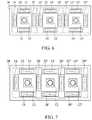
- the appearance inspecting devicefurther includes at least two image capturing devices, and at least two image capturing devices are arranged side by side on the carrying plate in one direction. Please refer to FIG. 4 and FIG. 6 .
- the three image capturing devices 22 , 22 ′, 22 ′′obtain the appearance image of different testing areas on the same component 46 respectively.
- the processor 28also selectively controls the image capturing devices 22 , 22 ′, 22 ′′ to turn on the light modules on the same side simultaneously (for example: the processor 28 simultaneously lights the light modules 14 , 14 ′, 14 ′′ or lights the light modules 18 , 18 ′, 18 ′′), to improve the detection efficiency.
- the image capturing device 22includes an image capture component 12 and light modules 14 , 16 , 18 , 20 around, and the light modules 14 , 16 , 18 , 20 that arranged in a rectangle.
- the image capturing device 22 ′includes an image capture component 12 ′ and light modules 14 ′, 16 ′, 18 ′, 20 ′ around the image capture component 12 ′, and the light modules 14 ′, 16 ′, 18 ′, 20 ′ is arranged in a rectangle.
- the image capturing device 22 ′′includes an image capture component 12 ′′ and light modules 14 ′′, 16 ′′, 18 ′′, 20 ′′ around the image capture component 12 ′′, and the light modules 14 ′′, 16 ′′, 18 ′′, 20 ′′ are arranged in rectangle.
- the processor 28controls the light modules 14 , 14 ′, 14 ′′ to simultaneously illuminate the component 46 , at this time, the image capture components 12 , 12 ′, 12 ′′ respectively captures appearance images.
- the processor 28controls the light modules 18 , 18 ′, 18 ′′ to simultaneously illuminate the component 46 , at this time, the image capture components 12 , 12 ′, 12 ′′ respectively captures appearance images.
- the processor 28controls the light modules 16 , 20 ′′ to simultaneously illuminate the component 46 , at this time, the image capture component 12 , 12 ′′ respectively captures an appearance image. Then, the processor 28 controls the light module 20 to illuminate the component 46 and controls the image capture component 12 to capture an appearance image. After that, the light module 16 ′ illuminates the component 46 and the image capture component 12 ′ captures an appearance image. Then, the processor 28 controls the light module 20 ′′ to illuminate the component 46 and controls the image capture component 12 ′ to capture an appearance image. Finally, the processor 28 controls the light module 16 ′′ to illuminate the component 46 and controls the image capture component 12 ′′ to capture an appearance image.
- each of the image capture components 12 , 12 ′, 12 ′′captures four pieces of the appearance image.
- the processor 28calculates and analyzes the four pieces of the appearance image captured by each of the image capture components 12 , 12 ′ and 12 ′′, three final images of different testing areas of the component 46 are obtained.
- any two adjacent image capturing devices of the image capturing devices 22 , 22 ′, 22 ′′share the same light module at the adjacent edge therebetween.
- FIG. 7Three image capturing devices 22 , 22 ′, 22 ′′ are disposed side by side on the carrying plate 26 in a direction.
- the image capturing device 22includes the image capture component 12 and the light modules 14 , 16 , 18 , 20 disposed around the image capture component 12 , and the light modules 14 , 16 , 18 , 20 arranged in a rectangle.
- the image capturing device 22 ′ and the image capturing device 22share the same light module 20 located at the adjacent side therebetween.
- the image capturing device 22 ′includes the image capture component 12 ′ and the light modules 14 ′, 20 , 18 ′, and 20 ′ around the image capture component 12 ′ and arranged in a rectangle.
- the image capturing device 22 ′ and the adjacent image capturing device 22 ′′share the light module 20 ′ located at the adjacent side therebetween.
- the image capturing device 22 ′′includes the image capture component 12 ′′ and the light modules 14 ′′, 20 ′, 18 ′′, 20 ′′ around the image capture component 12 ′′ and arranged in a rectangle.
- the processor 28controls each of the image capture components 12 , 12 ′, 12 ′′ of the image capturing devices 22 , 22 ′, 22 ′′ to capture images and performs subsequent operations.
- the detailed operationis the same as the aforementioned FIG. 6 embodiment, and will not be repeated here.
- the number of the image capturing deviceis equal to or more than two, the number of the image capturing devices is selected according to the size of the component to be tested, and at least two of the image capturing devices of the appearance inspecting device are disposed on the double-axis moving mechanism longitudinally or laterally.
- the image capturing device and the appearance inspecting device including the same disclosed in this disclosureinclude a plurality of light modules and at least one image capturing element and provide a complete appearance image by alternately turning on a plurality of light modules and controlling the image capturing element to capture a plurality of appearance images.
- the image capturing device disclosed hereinprovides complete appearance images automatically, thus increases the efficiency of defect detection.
Landscapes
- Engineering & Computer Science (AREA)
- Multimedia (AREA)
- Signal Processing (AREA)
- Physics & Mathematics (AREA)
- Health & Medical Sciences (AREA)
- Life Sciences & Earth Sciences (AREA)
- Chemical & Material Sciences (AREA)
- Analytical Chemistry (AREA)
- Biochemistry (AREA)
- General Health & Medical Sciences (AREA)
- General Physics & Mathematics (AREA)
- Immunology (AREA)
- Pathology (AREA)
- Investigating Materials By The Use Of Optical Means Adapted For Particular Applications (AREA)
- Image Input (AREA)
Abstract
Description
- This application claims the priority benefit of Taiwan applications serial No. 108140159, filed on Nov. 5, 2019. The entirety of the above-mentioned patent application is hereby incorporated by reference and made a part of specification.
- The invention relates to an image capturing device.
- When a product is performed an appearance defect detection, the reflective problem of the captured image of the product is occurred with reflective materials, and therefore the appearance details of the product is hard to be seen by the captured image. In addition, some appearance defects need to be inspected at various reflection angles, which means a lot of manual time is required for angles adjustment repeatedly to do the inspections, and is very time-consuming, labor-intensive, and the detection efficiency is not improved.
- According to the first aspect, an image capturing device is provided. The image capturing device includes an image capture component and N light modules. The image capture component is configured to capture an appearance image of a component. The N light modules are disposed around the image capture component, to be turned on alternately, and N4. When at least one of the N light modules is turned on, the image capture component captures the appearance image of the component.

- According to the second aspect, an appearance inspecting device is provided. The appearance inspecting device includes at least two image capturing devices arranged side by side in one direction. Each of the image capturing devices includes an image capture component and N light modules. The image capture component is configured to capture an appearance image of a component. The N light modules are disposed around the image capture component, to be turned on alternately, and N4. When at least one of the N light modules is turned on, the image capture component captures the appearance image of the component.
- In summary, the image capturing device and the appearance inspecting device including the same disclosed in this disclosure include a plurality of light modules and at least one image capturing element and provide a complete appearance image by alternately turning on a plurality of light modules and controlling the image capturing element to capture a plurality of appearance images. The image capturing device disclosed herein provides complete appearance images automatically, thus increases the efficiency of defect detection.
- These and other features, aspects and advantages of the present invention will become better understood with regard to the following description, appended claims, and accompanying drawings.
FIG. 1 is a three-dimensional schematic diagram of an image capturing device of an embodiment;FIG. 2 is a schematic circuit diagram of an appearance inspecting device of an embodiment;FIG. 3 is a schematic structural view of an appearance inspecting device having an image capturing device according to an embodiment;FIG. 4 is a schematic structural view of an appearance inspecting device during detection according to an embodiment;FIG. 5 is a three-dimensional schematic diagram of an image capturing device of an embodiment;FIG. 6 is a partial structural diagram of an appearance inspecting device of an embodiment;FIG. 7 is a partial structural diagram of an appearance inspecting device of an embodiment.- Please refer to
FIG. 1 . Animage capturing device 10 includes animage capture component 12 and N light modules, wherein N4 and is an even number. In this embodiment, N is equal to 4, that is, the fourlight modules image capture component 12 captures the appearance image of a component. Thelight modules image capture component 12 in a rectangle. Each of thelight modules light modules image capture component 12 captures the appearance image of the component46 (as shown inFIG. 4 ). In one embodiment, theimage capture component 12 cooperates with thelight modules light modules image capturing device 10 further includes acarrying plate 26, and theimage capture component 12 and thelight modules image capture component 12 are all disposed on the surface of thecarrying plate 26. - In one embodiment, the
image capture component 12 is a camera or a video camera. Thelight modules - Please refer to
FIG. 1 andFIG. 2 . Theimage capture component 12 and thelight modules processor 28. In an embodiment, theprocessor 28 controls thelight modules image capture component 12 to capture the appearance image of the component respectively when thelight modules - In one embodiment, the
processor 28 is a system on chip (SoC), a microcontroller (MCU), a central the processor (CPU), or a special application integrated circuit (ASIC). In one embodiment, theprocessor 28 is a processor of a desktop, a laptop, a tablet, or a smartphone. - Please refer to
FIG. 1 toFIG. 4 . Theappearance inspecting device 40 includes theimage capturing device 10, a double-axis moving mechanism 42 and amobile platform 44. Theprocessor 28 is electrically connected to the double-axis moving mechanism 42 and themobile platform 44, to control the double-axis moving mechanism 42 and themobile platform 44, respectively. The image capturingdevice 10 is disposed on the double-axis moving mechanism 42, and the double-axis moving mechanism 42 drives theimage capturing device 10 to move left and right in a first direction (such as the X-axis direction) and to move up and down in a second direction (such as the Z-axis direction). When the double-axis moving mechanism 42 drives theimage capturing device 10 to move up and down in the Z-axis direction, the range of thecomponent 46 covered by the light emitted from thelight modules image capturing device 10 up and down. Themobile platform 44 is disposed under theimage capturing device 10. In an embodiment, acomponent 46 is placed on themobile platform 44, and themobile platform 44 drives thecomponent 46 to move back and forth in a third direction (such as the Y-axis direction). In this way, through the cooperation of the double-axis moving mechanism 42 and themobile platform 44, three-axis relative movement is performed to locate theimage capturing device 10 above thecomponent 46 for capturing image. - Please refer to
FIG. 1 toFIG. 4 . When the double-axis moving mechanism 42 drives theimage capturing device 10 and themobile platform 44 drives thecomponent 46 to move to a testing position, theimage capturing device 10 is located above the testing area of thecomponent 46. Then, theprocessor 28 controls thelight modules image capture component 12 to respectively capture the appearance image of the testing area of the component when thelight modules image capture component 12 captures the first appearance image when theprocessor 28 controls thelight module 14 to illuminate thecomponent 46. Theimage capture component 12 captures the second appearance image when theprocessor 28 controls thelight module 16 to illuminate thecomponent 46. Theimage capture component 12 captures the third appearance image when theprocessor 28 controls thelight module 18 to illuminate thecomponent 46. Theimage capture component 12 captures the fourth appearance image when theprocessor 28 controls thelight module 20 to illuminate thecomponent 46. When there are N light modules, theimage capture component 12 captures at least N appearance images at the same position of thecomponent 46, and N is equal to 4 in this embodiment. - When capturing at least N pieces of the appearance image (that is, the first appearance image to the fourth appearance image), the
processor 28 obtains at least N pixels corresponding to each pixel position from at least N pieces of the appearance image. In other words, theprocessor 28 respectively obtains a pixel at the same pixel position of the first appearance image to the fourth appearance image. As there are four appearance images, there are four pixels in the same pixel position. Then, theprocessor 28 obtains the best pixel color of each pixel position according to the at least N pixels and a calculation program to generate a final image. In the calculation program, theprocessor 28 first sorts the four pixels according to the brightness of the four pixels (such as from the brightest pixel to the darkest pixel), discards the darkest and brightest pixels, and takes the average of the colors (RGB) of the pixels with intermediate brightness as the best pixel color of the corresponding pixel position. Since the best pixel colors of all the pixel positions are obtained, a clear final image is also obtained. In this embodiment, since the final image is composed of the best pixel colors obtained from the four appearance images, the final image is actually a clear image. When there is a defect on thecomponent 46, the defect is clearly shown on the final image, so the appearance defect detection is completed based on the final image by the computer (the processor). - In an embodiment, the
processor 28 selectively controls thelight modules light modules - In another embodiment, the
light modules image capturing device 10 is arranged in a circle. Please refer toFIG. 5 . Thelight modules plate 26 around theimage capture component 12. Each of thelight modules light modules image capture component 12 captures the appearance image of the testing area of the component respectively when thelight modules - In one embodiment, the appearance inspecting device further includes at least two image capturing devices, and at least two image capturing devices are arranged side by side on the carrying plate in one direction. Please refer to
FIG. 4 andFIG. 6 . In an embodiment, the threeimage capturing devices same component 46 respectively. Furthermore, theprocessor 28 also selectively controls theimage capturing devices processor 28 simultaneously lights thelight modules light modules image capturing device plate 26 side by side along one direction. Theimage capturing device 22 includes animage capture component 12 andlight modules light modules image capturing device 22′ includes animage capture component 12′ andlight modules 14′,16′,18′,20′ around theimage capture component 12′, and thelight modules 14′,16′,18′,20′ is arranged in a rectangle. Theimage capturing device 22″ includes animage capture component 12″ andlight modules 14″,16″,18″,20″ around theimage capture component 12″, and thelight modules 14″,16″,18″,20″ are arranged in rectangle. In one embodiment, theprocessor 28 controls thelight modules component 46, at this time, theimage capture components processor 28 controls thelight modules component 46, at this time, theimage capture components processor 28 controls thelight modules component 46, at this time, theimage capture component processor 28 controls thelight module 20 to illuminate thecomponent 46 and controls theimage capture component 12 to capture an appearance image. After that, thelight module 16′ illuminates thecomponent 46 and theimage capture component 12′ captures an appearance image. Then, theprocessor 28 controls thelight module 20″ to illuminate thecomponent 46 and controls theimage capture component 12′ to capture an appearance image. Finally, theprocessor 28 controls thelight module 16″ to illuminate thecomponent 46 and controls theimage capture component 12″ to capture an appearance image. In this way, each of theimage capture components processor 28 calculates and analyzes the four pieces of the appearance image captured by each of theimage capture components component 46 are obtained. - In one embodiment, in order to save space and the number of the light modules, any two adjacent image capturing devices of the
image capturing devices FIG. 7 . Threeimage capturing devices plate 26 in a direction. Theimage capturing device 22 includes theimage capture component 12 and thelight modules image capture component 12, and thelight modules image capturing device 22′ and theimage capturing device 22 share thesame light module 20 located at the adjacent side therebetween. Theimage capturing device 22′ includes theimage capture component 12′ and thelight modules 14′,20,18′, and20′ around theimage capture component 12′ and arranged in a rectangle. Theimage capturing device 22′ and the adjacentimage capturing device 22″ share thelight module 20′ located at the adjacent side therebetween. Theimage capturing device 22″ includes theimage capture component 12″ and thelight modules 14″,20′,18″,20″ around theimage capture component 12″ and arranged in a rectangle. Then, theprocessor 28 controls each of theimage capture components image capturing devices FIG. 6 embodiment, and will not be repeated here. - In an embodiment, the number of the image capturing device is equal to or more than two, the number of the image capturing devices is selected according to the size of the component to be tested, and at least two of the image capturing devices of the appearance inspecting device are disposed on the double-axis moving mechanism longitudinally or laterally.
- In sum, the image capturing device and the appearance inspecting device including the same disclosed in this disclosure include a plurality of light modules and at least one image capturing element and provide a complete appearance image by alternately turning on a plurality of light modules and controlling the image capturing element to capture a plurality of appearance images. The image capturing device disclosed herein provides complete appearance images automatically, thus increases the efficiency of defect detection.
- Although the present invention has been described in considerable detail with reference to certain preferred embodiments thereof, the disclosure is not for limiting the scope. Persons having ordinary skill in the art may make various modifications and changes without departing from the scope. Therefore, the scope of the appended claims should not be limited to the description of the preferred embodiments described above.
Claims (16)

Applications Claiming Priority (2)
| Application Number | Priority Date | Filing Date | Title |
|---|---|---|---|
| TW108140159ATW202119019A (en) | 2019-11-05 | 2019-11-05 | Appearance image capturing device and appearance detecting device including the same |
| TW108140159 | 2019-11-05 |
Publications (2)
| Publication Number | Publication Date |
|---|---|
| US20210136266A1true US20210136266A1 (en) | 2021-05-06 |
| US11575814B2 US11575814B2 (en) | 2023-02-07 |
Family
ID=75689157
Family Applications (1)
| Application Number | Title | Priority Date | Filing Date |
|---|---|---|---|
| US17/074,694ActiveUS11575814B2 (en) | 2019-11-05 | 2020-10-20 | Image capturing device and appearance inspecting device including the same |
Country Status (3)
| Country | Link |
|---|---|
| US (1) | US11575814B2 (en) |
| JP (1) | JP2021076569A (en) |
| TW (1) | TW202119019A (en) |
Cited By (1)
| Publication number | Priority date | Publication date | Assignee | Title |
|---|---|---|---|---|
| CN118397008A (en)* | 2024-06-28 | 2024-07-26 | 深圳雪峰电子有限公司 | Electronic detonator module appearance detection method and system based on image technology |
Citations (6)
| Publication number | Priority date | Publication date | Assignee | Title |
|---|---|---|---|---|
| US20070205357A1 (en)* | 2006-03-03 | 2007-09-06 | Fujitsu Limited | Image capturing apparatus |
| US20080205357A1 (en)* | 2007-02-28 | 2008-08-28 | Motorola, Inc. | Wireless wide area broadband coverage in a vehicular area network (van) |
| US7889251B1 (en)* | 2005-06-08 | 2011-02-15 | National Semiconductor Corporation | Method and device for white level calibration |
| US20190213748A1 (en)* | 2018-01-10 | 2019-07-11 | Omron Corporation | Image processing system |
| US20200053269A1 (en)* | 2015-05-27 | 2020-02-13 | Google Llc | Electronic Device with Adjustable Illumination |
| US20210096689A1 (en)* | 2019-09-27 | 2021-04-01 | Seiko Epson Corporation | Position detection device, projector, and position detection method |
Family Cites Families (25)
| Publication number | Priority date | Publication date | Assignee | Title |
|---|---|---|---|---|
| JPS52115279A (en)* | 1976-03-23 | 1977-09-27 | Matsushita Electric Ind Co Ltd | Gas analyzer |
| JPH07117454B2 (en)* | 1986-12-22 | 1995-12-18 | 株式会社島津製作所 | Spectrophotometer |
| US4981362A (en)* | 1989-10-16 | 1991-01-01 | Xerox Corporation | Particle concentration measuring method and device |
| JP3573512B2 (en)* | 1994-05-17 | 2004-10-06 | オリンパス株式会社 | Image processing method and image processing apparatus |
| US5926262A (en)* | 1997-07-01 | 1999-07-20 | Lj Laboratories, L.L.C. | Apparatus and method for measuring optical characteristics of an object |
| JPH10339697A (en)* | 1997-06-09 | 1998-12-22 | Kubota Corp | Lamp burnout detector of colorimetry analyzer |
| JP2007206797A (en) | 2006-01-31 | 2007-08-16 | Omron Corp | Image processing method and image processor |
| JP2007278713A (en)* | 2006-04-03 | 2007-10-25 | Chuo Denshi Keisoku Kk | Lighting method in coating inspecting device |
| JP2007335991A (en)* | 2006-06-12 | 2007-12-27 | Toshiba Corp | Signal processing circuit |
| JP2010181951A (en)* | 2009-02-03 | 2010-08-19 | Mitsubishi Electric Corp | Image processor and image processing program |
| US10084993B2 (en) | 2010-01-14 | 2018-09-25 | Verint Systems Ltd. | Systems and methods for managing and displaying video sources |
| JP5564349B2 (en)* | 2010-07-15 | 2014-07-30 | 株式会社キーエンス | Image processing apparatus and appearance inspection method |
| US8743275B1 (en)* | 2010-12-15 | 2014-06-03 | Google Inc. | Mobile communication device with multiple flashpoints |
| US10458903B2 (en)* | 2013-01-17 | 2019-10-29 | Koninklijke Philips N.V. | Method and apparatus for monitoring a level of a gaseous species of interest |
| US9036943B1 (en)* | 2013-03-14 | 2015-05-19 | Amazon Technologies, Inc. | Cloud-based image improvement |
| EP2999956B1 (en)* | 2013-05-23 | 2021-06-30 | Rina Consulting - Centro Sviluppo Materiali S.p.A. | Method for the surface inspection of long products and apparatus suitable for carrying out such a method |
| US10021295B1 (en)* | 2013-06-03 | 2018-07-10 | Amazon Technologies, Inc. | Visual cues for managing image capture |
| JP2015040796A (en)* | 2013-08-22 | 2015-03-02 | シャープ株式会社 | Defect detection device |
| JP6267481B2 (en)* | 2013-10-18 | 2018-01-24 | リコーエレメックス株式会社 | Appearance inspection apparatus and appearance inspection method |
| FR3016699B1 (en)* | 2014-01-22 | 2016-02-12 | Msc & Sgcc | METHOD AND DEVICE FOR THE DETECTION IN PARTICULAR OF REFRACTANT DEFECTS |
| JP6433268B2 (en)* | 2014-03-31 | 2018-12-05 | 国立大学法人 東京大学 | Inspection system and inspection method |
| JP6424020B2 (en) | 2014-06-09 | 2018-11-14 | 株式会社キーエンス | Image inspection apparatus, image inspection method, image inspection program, computer-readable recording medium, and recorded apparatus |
| JP6826814B2 (en)* | 2016-02-24 | 2021-02-10 | 旭化成エレクトロニクス株式会社 | Optical physical quantity measuring device and its light source control method |
| JP2018112478A (en)* | 2017-01-12 | 2018-07-19 | リコーエレメックス株式会社 | Image inspection device and image inspection method |
| US10542245B2 (en)* | 2017-05-24 | 2020-01-21 | Lg Electronics Inc. | Mobile terminal and method for controlling the same |
- 2019
- 2019-11-05TWTW108140159Apatent/TW202119019A/enunknown
- 2020
- 2020-01-15JPJP2020004240Apatent/JP2021076569A/enactivePending
- 2020-10-20USUS17/074,694patent/US11575814B2/enactiveActive
Patent Citations (6)
| Publication number | Priority date | Publication date | Assignee | Title |
|---|---|---|---|---|
| US7889251B1 (en)* | 2005-06-08 | 2011-02-15 | National Semiconductor Corporation | Method and device for white level calibration |
| US20070205357A1 (en)* | 2006-03-03 | 2007-09-06 | Fujitsu Limited | Image capturing apparatus |
| US20080205357A1 (en)* | 2007-02-28 | 2008-08-28 | Motorola, Inc. | Wireless wide area broadband coverage in a vehicular area network (van) |
| US20200053269A1 (en)* | 2015-05-27 | 2020-02-13 | Google Llc | Electronic Device with Adjustable Illumination |
| US20190213748A1 (en)* | 2018-01-10 | 2019-07-11 | Omron Corporation | Image processing system |
| US20210096689A1 (en)* | 2019-09-27 | 2021-04-01 | Seiko Epson Corporation | Position detection device, projector, and position detection method |
Cited By (1)
| Publication number | Priority date | Publication date | Assignee | Title |
|---|---|---|---|---|
| CN118397008A (en)* | 2024-06-28 | 2024-07-26 | 深圳雪峰电子有限公司 | Electronic detonator module appearance detection method and system based on image technology |
Also Published As
| Publication number | Publication date |
|---|---|
| TW202119019A (en) | 2021-05-16 |
| US11575814B2 (en) | 2023-02-07 |
| JP2021076569A (en) | 2021-05-20 |
Similar Documents
| Publication | Publication Date | Title |
|---|---|---|
| US10805552B2 (en) | Visual inspection device and illumination condition setting method of visual inspection device | |
| US8363929B2 (en) | Shape measurement apparatus and calibration method | |
| JP2013505464A (en) | High speed optical inspection system with camera array and compact built-in illuminator | |
| CN101539529A (en) | Light source system for online detection of minitype fruits based on LED | |
| WO2013081882A1 (en) | High speed, high resolution, three dimensional printed circuit board inspection system | |
| US20170019578A1 (en) | Inspecting device and method for inspecting inspection target | |
| JP2015068668A (en) | Appearance inspection device | |
| US11971367B2 (en) | Inspection device and inspection method | |
| CN105277574A (en) | Multi-exposure image mixing detection method applying repeated exposure | |
| US10215707B2 (en) | System for inspecting a backside of a wafer | |
| US11575814B2 (en) | Image capturing device and appearance inspecting device including the same | |
| US11170518B2 (en) | Inspection device for generating height data of a measurement target | |
| JP2018179789A (en) | Inspection apparatus, inspection method, and article manufacturing method | |
| TWI687672B (en) | Optical inspection system and image processing method thereof | |
| TWM514002U (en) | Optical inspection device | |
| US10986283B2 (en) | Device for inspecting mask plate, method for inspecting mask plate, and corresponding method for controlling light sources | |
| CN107959801A (en) | A kind of light-source brightness control system and control method | |
| TW202109027A (en) | Wafer appearance inspection device and method | |
| JP6067407B2 (en) | Inspection device | |
| CN111351797A (en) | Single-side and double-side detection system and paired reflector set device | |
| CN112763493A (en) | Appearance image capturing device and appearance detection device comprising same | |
| TW201913045A (en) | Optical path detecting device and detecting method thereof capable of achieving the purpose of fast, accurate, time-saving and labor-saving detection | |
| JP2012169370A (en) | Display panel inspection equipment and display panel inspection method | |
| TWI290223B (en) | Adjustable light sources for image forming apparatus | |
| JP2016118518A (en) | Appearance inspection device |
Legal Events
| Date | Code | Title | Description |
|---|---|---|---|
| AS | Assignment | Owner name:ASUSTEK COMPUTER INC., TAIWAN Free format text:ASSIGNMENT OF ASSIGNORS INTEREST;ASSIGNOR:LIU, KUAN-LIN;REEL/FRAME:054102/0981 Effective date:20201020 | |
| FEPP | Fee payment procedure | Free format text:ENTITY STATUS SET TO UNDISCOUNTED (ORIGINAL EVENT CODE: BIG.); ENTITY STATUS OF PATENT OWNER: LARGE ENTITY | |
| STPP | Information on status: patent application and granting procedure in general | Free format text:DOCKETED NEW CASE - READY FOR EXAMINATION | |
| STPP | Information on status: patent application and granting procedure in general | Free format text:NON FINAL ACTION MAILED | |
| STPP | Information on status: patent application and granting procedure in general | Free format text:RESPONSE TO NON-FINAL OFFICE ACTION ENTERED AND FORWARDED TO EXAMINER | |
| STPP | Information on status: patent application and granting procedure in general | Free format text:FINAL REJECTION MAILED | |
| STPP | Information on status: patent application and granting procedure in general | Free format text:DOCKETED NEW CASE - READY FOR EXAMINATION | |
| STPP | Information on status: patent application and granting procedure in general | Free format text:NOTICE OF ALLOWANCE MAILED -- APPLICATION RECEIVED IN OFFICE OF PUBLICATIONS | |
| STPP | Information on status: patent application and granting procedure in general | Free format text:PUBLICATIONS -- ISSUE FEE PAYMENT RECEIVED | |
| STCF | Information on status: patent grant | Free format text:PATENTED CASE |