US20210098412A1 - Direct gang bonding methods and structures - Google Patents
Direct gang bonding methods and structuresDownload PDFInfo
- Publication number
- US20210098412A1 US20210098412A1US16/874,527US202016874527AUS2021098412A1US 20210098412 A1US20210098412 A1US 20210098412A1US 202016874527 AUS202016874527 AUS 202016874527AUS 2021098412 A1US2021098412 A1US 2021098412A1
- Authority
- US
- United States
- Prior art keywords
- elements
- dielectric layer
- bonding
- bonded
- bonded structure
- Prior art date
- Legal status (The legal status is an assumption and is not a legal conclusion. Google has not performed a legal analysis and makes no representation as to the accuracy of the status listed.)
- Granted
Links
Images


Classifications
- H—ELECTRICITY
- H01—ELECTRIC ELEMENTS
- H01L—SEMICONDUCTOR DEVICES NOT COVERED BY CLASS H10
- H01L21/00—Processes or apparatus adapted for the manufacture or treatment of semiconductor or solid state devices or of parts thereof
- H01L21/67—Apparatus specially adapted for handling semiconductor or electric solid state devices during manufacture or treatment thereof; Apparatus specially adapted for handling wafers during manufacture or treatment of semiconductor or electric solid state devices or components ; Apparatus not specifically provided for elsewhere
- H01L21/683—Apparatus specially adapted for handling semiconductor or electric solid state devices during manufacture or treatment thereof; Apparatus specially adapted for handling wafers during manufacture or treatment of semiconductor or electric solid state devices or components ; Apparatus not specifically provided for elsewhere for supporting or gripping
- H01L21/6835—Apparatus specially adapted for handling semiconductor or electric solid state devices during manufacture or treatment thereof; Apparatus specially adapted for handling wafers during manufacture or treatment of semiconductor or electric solid state devices or components ; Apparatus not specifically provided for elsewhere for supporting or gripping using temporarily an auxiliary support
- H—ELECTRICITY
- H01—ELECTRIC ELEMENTS
- H01L—SEMICONDUCTOR DEVICES NOT COVERED BY CLASS H10
- H01L24/00—Arrangements for connecting or disconnecting semiconductor or solid-state bodies; Methods or apparatus related thereto
- H01L24/01—Means for bonding being attached to, or being formed on, the surface to be connected, e.g. chip-to-package, die-attach, "first-level" interconnects; Manufacturing methods related thereto
- H01L24/26—Layer connectors, e.g. plate connectors, solder or adhesive layers; Manufacturing methods related thereto
- H01L24/31—Structure, shape, material or disposition of the layer connectors after the connecting process
- H01L24/32—Structure, shape, material or disposition of the layer connectors after the connecting process of an individual layer connector
- H—ELECTRICITY
- H01—ELECTRIC ELEMENTS
- H01L—SEMICONDUCTOR DEVICES NOT COVERED BY CLASS H10
- H01L23/00—Details of semiconductor or other solid state devices
- H01L23/28—Encapsulations, e.g. encapsulating layers, coatings, e.g. for protection
- H01L23/31—Encapsulations, e.g. encapsulating layers, coatings, e.g. for protection characterised by the arrangement or shape
- H01L23/3107—Encapsulations, e.g. encapsulating layers, coatings, e.g. for protection characterised by the arrangement or shape the device being completely enclosed
- H—ELECTRICITY
- H01—ELECTRIC ELEMENTS
- H01L—SEMICONDUCTOR DEVICES NOT COVERED BY CLASS H10
- H01L23/00—Details of semiconductor or other solid state devices
- H01L23/28—Encapsulations, e.g. encapsulating layers, coatings, e.g. for protection
- H01L23/31—Encapsulations, e.g. encapsulating layers, coatings, e.g. for protection characterised by the arrangement or shape
- H01L23/3157—Partial encapsulation or coating
- H01L23/3185—Partial encapsulation or coating the coating covering also the sidewalls of the semiconductor body
- H—ELECTRICITY
- H01—ELECTRIC ELEMENTS
- H01L—SEMICONDUCTOR DEVICES NOT COVERED BY CLASS H10
- H01L24/00—Arrangements for connecting or disconnecting semiconductor or solid-state bodies; Methods or apparatus related thereto
- H01L24/01—Means for bonding being attached to, or being formed on, the surface to be connected, e.g. chip-to-package, die-attach, "first-level" interconnects; Manufacturing methods related thereto
- H01L24/02—Bonding areas ; Manufacturing methods related thereto
- H01L24/07—Structure, shape, material or disposition of the bonding areas after the connecting process
- H01L24/08—Structure, shape, material or disposition of the bonding areas after the connecting process of an individual bonding area
- H—ELECTRICITY
- H01—ELECTRIC ELEMENTS
- H01L—SEMICONDUCTOR DEVICES NOT COVERED BY CLASS H10
- H01L24/00—Arrangements for connecting or disconnecting semiconductor or solid-state bodies; Methods or apparatus related thereto
- H01L24/01—Means for bonding being attached to, or being formed on, the surface to be connected, e.g. chip-to-package, die-attach, "first-level" interconnects; Manufacturing methods related thereto
- H01L24/26—Layer connectors, e.g. plate connectors, solder or adhesive layers; Manufacturing methods related thereto
- H01L24/27—Manufacturing methods
- H—ELECTRICITY
- H01—ELECTRIC ELEMENTS
- H01L—SEMICONDUCTOR DEVICES NOT COVERED BY CLASS H10
- H01L24/00—Arrangements for connecting or disconnecting semiconductor or solid-state bodies; Methods or apparatus related thereto
- H01L24/01—Means for bonding being attached to, or being formed on, the surface to be connected, e.g. chip-to-package, die-attach, "first-level" interconnects; Manufacturing methods related thereto
- H01L24/26—Layer connectors, e.g. plate connectors, solder or adhesive layers; Manufacturing methods related thereto
- H01L24/28—Structure, shape, material or disposition of the layer connectors prior to the connecting process
- H01L24/29—Structure, shape, material or disposition of the layer connectors prior to the connecting process of an individual layer connector
- H—ELECTRICITY
- H01—ELECTRIC ELEMENTS
- H01L—SEMICONDUCTOR DEVICES NOT COVERED BY CLASS H10
- H01L24/00—Arrangements for connecting or disconnecting semiconductor or solid-state bodies; Methods or apparatus related thereto
- H01L24/80—Methods for connecting semiconductor or other solid state bodies using means for bonding being attached to, or being formed on, the surface to be connected
- H01L24/83—Methods for connecting semiconductor or other solid state bodies using means for bonding being attached to, or being formed on, the surface to be connected using a layer connector
- H—ELECTRICITY
- H01—ELECTRIC ELEMENTS
- H01L—SEMICONDUCTOR DEVICES NOT COVERED BY CLASS H10
- H01L25/00—Assemblies consisting of a plurality of semiconductor or other solid state devices
- H01L25/03—Assemblies consisting of a plurality of semiconductor or other solid state devices all the devices being of a type provided for in a single subclass of subclasses H10B, H10D, H10F, H10H, H10K or H10N, e.g. assemblies of rectifier diodes
- H01L25/04—Assemblies consisting of a plurality of semiconductor or other solid state devices all the devices being of a type provided for in a single subclass of subclasses H10B, H10D, H10F, H10H, H10K or H10N, e.g. assemblies of rectifier diodes the devices not having separate containers
- H01L25/065—Assemblies consisting of a plurality of semiconductor or other solid state devices all the devices being of a type provided for in a single subclass of subclasses H10B, H10D, H10F, H10H, H10K or H10N, e.g. assemblies of rectifier diodes the devices not having separate containers the devices being of a type provided for in group H10D89/00
- H01L25/0657—Stacked arrangements of devices
- H—ELECTRICITY
- H01—ELECTRIC ELEMENTS
- H01L—SEMICONDUCTOR DEVICES NOT COVERED BY CLASS H10
- H01L2221/00—Processes or apparatus adapted for the manufacture or treatment of semiconductor or solid state devices or of parts thereof covered by H01L21/00
- H01L2221/67—Apparatus for handling semiconductor or electric solid state devices during manufacture or treatment thereof; Apparatus for handling wafers during manufacture or treatment of semiconductor or electric solid state devices or components; Apparatus not specifically provided for elsewhere
- H01L2221/683—Apparatus for handling semiconductor or electric solid state devices during manufacture or treatment thereof; Apparatus for handling wafers during manufacture or treatment of semiconductor or electric solid state devices or components; Apparatus not specifically provided for elsewhere for supporting or gripping
- H01L2221/68304—Apparatus for handling semiconductor or electric solid state devices during manufacture or treatment thereof; Apparatus for handling wafers during manufacture or treatment of semiconductor or electric solid state devices or components; Apparatus not specifically provided for elsewhere for supporting or gripping using temporarily an auxiliary support
- H01L2221/68354—Apparatus for handling semiconductor or electric solid state devices during manufacture or treatment thereof; Apparatus for handling wafers during manufacture or treatment of semiconductor or electric solid state devices or components; Apparatus not specifically provided for elsewhere for supporting or gripping using temporarily an auxiliary support used to support diced chips prior to mounting
- H—ELECTRICITY
- H01—ELECTRIC ELEMENTS
- H01L—SEMICONDUCTOR DEVICES NOT COVERED BY CLASS H10
- H01L2224/00—Indexing scheme for arrangements for connecting or disconnecting semiconductor or solid-state bodies and methods related thereto as covered by H01L24/00
- H01L2224/01—Means for bonding being attached to, or being formed on, the surface to be connected, e.g. chip-to-package, die-attach, "first-level" interconnects; Manufacturing methods related thereto
- H01L2224/02—Bonding areas; Manufacturing methods related thereto
- H01L2224/07—Structure, shape, material or disposition of the bonding areas after the connecting process
- H01L2224/08—Structure, shape, material or disposition of the bonding areas after the connecting process of an individual bonding area
- H01L2224/081—Disposition
- H01L2224/0812—Disposition the bonding area connecting directly to another bonding area, i.e. connectorless bonding, e.g. bumpless bonding
- H01L2224/08135—Disposition the bonding area connecting directly to another bonding area, i.e. connectorless bonding, e.g. bumpless bonding the bonding area connecting between different semiconductor or solid-state bodies, i.e. chip-to-chip
- H01L2224/08145—Disposition the bonding area connecting directly to another bonding area, i.e. connectorless bonding, e.g. bumpless bonding the bonding area connecting between different semiconductor or solid-state bodies, i.e. chip-to-chip the bodies being stacked
- H01L2224/08146—Disposition the bonding area connecting directly to another bonding area, i.e. connectorless bonding, e.g. bumpless bonding the bonding area connecting between different semiconductor or solid-state bodies, i.e. chip-to-chip the bodies being stacked the bonding area connecting to a via connection in the body
- H—ELECTRICITY
- H01—ELECTRIC ELEMENTS
- H01L—SEMICONDUCTOR DEVICES NOT COVERED BY CLASS H10
- H01L2224/00—Indexing scheme for arrangements for connecting or disconnecting semiconductor or solid-state bodies and methods related thereto as covered by H01L24/00
- H01L2224/01—Means for bonding being attached to, or being formed on, the surface to be connected, e.g. chip-to-package, die-attach, "first-level" interconnects; Manufacturing methods related thereto
- H01L2224/02—Bonding areas; Manufacturing methods related thereto
- H01L2224/07—Structure, shape, material or disposition of the bonding areas after the connecting process
- H01L2224/09—Structure, shape, material or disposition of the bonding areas after the connecting process of a plurality of bonding areas
- H01L2224/091—Disposition
- H01L2224/0918—Disposition being disposed on at least two different sides of the body, e.g. dual array
- H01L2224/09181—On opposite sides of the body
- H—ELECTRICITY
- H01—ELECTRIC ELEMENTS
- H01L—SEMICONDUCTOR DEVICES NOT COVERED BY CLASS H10
- H01L2224/00—Indexing scheme for arrangements for connecting or disconnecting semiconductor or solid-state bodies and methods related thereto as covered by H01L24/00
- H01L2224/01—Means for bonding being attached to, or being formed on, the surface to be connected, e.g. chip-to-package, die-attach, "first-level" interconnects; Manufacturing methods related thereto
- H01L2224/26—Layer connectors, e.g. plate connectors, solder or adhesive layers; Manufacturing methods related thereto
- H01L2224/28—Structure, shape, material or disposition of the layer connectors prior to the connecting process
- H01L2224/29—Structure, shape, material or disposition of the layer connectors prior to the connecting process of an individual layer connector
- H01L2224/29001—Core members of the layer connector
- H01L2224/29099—Material
- H01L2224/29186—Material with a principal constituent of the material being a non metallic, non metalloid inorganic material
- H01L2224/29187—Ceramics, e.g. crystalline carbides, nitrides or oxides
- H—ELECTRICITY
- H01—ELECTRIC ELEMENTS
- H01L—SEMICONDUCTOR DEVICES NOT COVERED BY CLASS H10
- H01L2224/00—Indexing scheme for arrangements for connecting or disconnecting semiconductor or solid-state bodies and methods related thereto as covered by H01L24/00
- H01L2224/01—Means for bonding being attached to, or being formed on, the surface to be connected, e.g. chip-to-package, die-attach, "first-level" interconnects; Manufacturing methods related thereto
- H01L2224/26—Layer connectors, e.g. plate connectors, solder or adhesive layers; Manufacturing methods related thereto
- H01L2224/31—Structure, shape, material or disposition of the layer connectors after the connecting process
- H01L2224/32—Structure, shape, material or disposition of the layer connectors after the connecting process of an individual layer connector
- H01L2224/321—Disposition
- H01L2224/32135—Disposition the layer connector connecting between different semiconductor or solid-state bodies, i.e. chip-to-chip
- H01L2224/32145—Disposition the layer connector connecting between different semiconductor or solid-state bodies, i.e. chip-to-chip the bodies being stacked
- H—ELECTRICITY
- H01—ELECTRIC ELEMENTS
- H01L—SEMICONDUCTOR DEVICES NOT COVERED BY CLASS H10
- H01L2224/00—Indexing scheme for arrangements for connecting or disconnecting semiconductor or solid-state bodies and methods related thereto as covered by H01L24/00
- H01L2224/01—Means for bonding being attached to, or being formed on, the surface to be connected, e.g. chip-to-package, die-attach, "first-level" interconnects; Manufacturing methods related thereto
- H01L2224/26—Layer connectors, e.g. plate connectors, solder or adhesive layers; Manufacturing methods related thereto
- H01L2224/31—Structure, shape, material or disposition of the layer connectors after the connecting process
- H01L2224/32—Structure, shape, material or disposition of the layer connectors after the connecting process of an individual layer connector
- H01L2224/321—Disposition
- H01L2224/32151—Disposition the layer connector connecting between a semiconductor or solid-state body and an item not being a semiconductor or solid-state body, e.g. chip-to-substrate, chip-to-passive
- H01L2224/32221—Disposition the layer connector connecting between a semiconductor or solid-state body and an item not being a semiconductor or solid-state body, e.g. chip-to-substrate, chip-to-passive the body and the item being stacked
- H01L2224/32225—Disposition the layer connector connecting between a semiconductor or solid-state body and an item not being a semiconductor or solid-state body, e.g. chip-to-substrate, chip-to-passive the body and the item being stacked the item being non-metallic, e.g. insulating substrate with or without metallisation
- H—ELECTRICITY
- H01—ELECTRIC ELEMENTS
- H01L—SEMICONDUCTOR DEVICES NOT COVERED BY CLASS H10
- H01L2224/00—Indexing scheme for arrangements for connecting or disconnecting semiconductor or solid-state bodies and methods related thereto as covered by H01L24/00
- H01L2224/80—Methods for connecting semiconductor or other solid state bodies using means for bonding being attached to, or being formed on, the surface to be connected
- H01L2224/80001—Methods for connecting semiconductor or other solid state bodies using means for bonding being attached to, or being formed on, the surface to be connected by connecting a bonding area directly to another bonding area, i.e. connectorless bonding, e.g. bumpless bonding
- H01L2224/80003—Methods for connecting semiconductor or other solid state bodies using means for bonding being attached to, or being formed on, the surface to be connected by connecting a bonding area directly to another bonding area, i.e. connectorless bonding, e.g. bumpless bonding involving a temporary auxiliary member not forming part of the bonding apparatus
- H01L2224/80006—Methods for connecting semiconductor or other solid state bodies using means for bonding being attached to, or being formed on, the surface to be connected by connecting a bonding area directly to another bonding area, i.e. connectorless bonding, e.g. bumpless bonding involving a temporary auxiliary member not forming part of the bonding apparatus being a temporary or sacrificial substrate
- H—ELECTRICITY
- H01—ELECTRIC ELEMENTS
- H01L—SEMICONDUCTOR DEVICES NOT COVERED BY CLASS H10
- H01L2224/00—Indexing scheme for arrangements for connecting or disconnecting semiconductor or solid-state bodies and methods related thereto as covered by H01L24/00
- H01L2224/80—Methods for connecting semiconductor or other solid state bodies using means for bonding being attached to, or being formed on, the surface to be connected
- H01L2224/80001—Methods for connecting semiconductor or other solid state bodies using means for bonding being attached to, or being formed on, the surface to be connected by connecting a bonding area directly to another bonding area, i.e. connectorless bonding, e.g. bumpless bonding
- H01L2224/80009—Pre-treatment of the bonding area
- H01L2224/8001—Cleaning the bonding area, e.g. oxide removal step, desmearing
- H01L2224/80013—Plasma cleaning
- H—ELECTRICITY
- H01—ELECTRIC ELEMENTS
- H01L—SEMICONDUCTOR DEVICES NOT COVERED BY CLASS H10
- H01L2224/00—Indexing scheme for arrangements for connecting or disconnecting semiconductor or solid-state bodies and methods related thereto as covered by H01L24/00
- H01L2224/80—Methods for connecting semiconductor or other solid state bodies using means for bonding being attached to, or being formed on, the surface to be connected
- H01L2224/80001—Methods for connecting semiconductor or other solid state bodies using means for bonding being attached to, or being formed on, the surface to be connected by connecting a bonding area directly to another bonding area, i.e. connectorless bonding, e.g. bumpless bonding
- H01L2224/80009—Pre-treatment of the bonding area
- H01L2224/8003—Reshaping the bonding area in the bonding apparatus, e.g. flattening the bonding area
- H01L2224/80047—Reshaping the bonding area in the bonding apparatus, e.g. flattening the bonding area by mechanical means, e.g. severing, pressing, stamping
- H—ELECTRICITY
- H01—ELECTRIC ELEMENTS
- H01L—SEMICONDUCTOR DEVICES NOT COVERED BY CLASS H10
- H01L2224/00—Indexing scheme for arrangements for connecting or disconnecting semiconductor or solid-state bodies and methods related thereto as covered by H01L24/00
- H01L2224/80—Methods for connecting semiconductor or other solid state bodies using means for bonding being attached to, or being formed on, the surface to be connected
- H01L2224/80001—Methods for connecting semiconductor or other solid state bodies using means for bonding being attached to, or being formed on, the surface to be connected by connecting a bonding area directly to another bonding area, i.e. connectorless bonding, e.g. bumpless bonding
- H01L2224/80009—Pre-treatment of the bonding area
- H01L2224/80048—Thermal treatments, e.g. annealing, controlled pre-heating or pre-cooling
- H—ELECTRICITY
- H01—ELECTRIC ELEMENTS
- H01L—SEMICONDUCTOR DEVICES NOT COVERED BY CLASS H10
- H01L2224/00—Indexing scheme for arrangements for connecting or disconnecting semiconductor or solid-state bodies and methods related thereto as covered by H01L24/00
- H01L2224/80—Methods for connecting semiconductor or other solid state bodies using means for bonding being attached to, or being formed on, the surface to be connected
- H01L2224/80001—Methods for connecting semiconductor or other solid state bodies using means for bonding being attached to, or being formed on, the surface to be connected by connecting a bonding area directly to another bonding area, i.e. connectorless bonding, e.g. bumpless bonding
- H01L2224/80053—Bonding environment
- H01L2224/80095—Temperature settings
- H01L2224/80096—Transient conditions
- H01L2224/80097—Heating
- H—ELECTRICITY
- H01—ELECTRIC ELEMENTS
- H01L—SEMICONDUCTOR DEVICES NOT COVERED BY CLASS H10
- H01L2224/00—Indexing scheme for arrangements for connecting or disconnecting semiconductor or solid-state bodies and methods related thereto as covered by H01L24/00
- H01L2224/80—Methods for connecting semiconductor or other solid state bodies using means for bonding being attached to, or being formed on, the surface to be connected
- H01L2224/80001—Methods for connecting semiconductor or other solid state bodies using means for bonding being attached to, or being formed on, the surface to be connected by connecting a bonding area directly to another bonding area, i.e. connectorless bonding, e.g. bumpless bonding
- H01L2224/80053—Bonding environment
- H01L2224/80095—Temperature settings
- H01L2224/80099—Ambient temperature
- H—ELECTRICITY
- H01—ELECTRIC ELEMENTS
- H01L—SEMICONDUCTOR DEVICES NOT COVERED BY CLASS H10
- H01L2224/00—Indexing scheme for arrangements for connecting or disconnecting semiconductor or solid-state bodies and methods related thereto as covered by H01L24/00
- H01L2224/80—Methods for connecting semiconductor or other solid state bodies using means for bonding being attached to, or being formed on, the surface to be connected
- H01L2224/80001—Methods for connecting semiconductor or other solid state bodies using means for bonding being attached to, or being formed on, the surface to be connected by connecting a bonding area directly to another bonding area, i.e. connectorless bonding, e.g. bumpless bonding
- H01L2224/80905—Combinations of bonding methods provided for in at least two different groups from H01L2224/808 - H01L2224/80904
- H01L2224/80906—Specific sequence of method steps
- H—ELECTRICITY
- H01—ELECTRIC ELEMENTS
- H01L—SEMICONDUCTOR DEVICES NOT COVERED BY CLASS H10
- H01L2224/00—Indexing scheme for arrangements for connecting or disconnecting semiconductor or solid-state bodies and methods related thereto as covered by H01L24/00
- H01L2224/80—Methods for connecting semiconductor or other solid state bodies using means for bonding being attached to, or being formed on, the surface to be connected
- H01L2224/80001—Methods for connecting semiconductor or other solid state bodies using means for bonding being attached to, or being formed on, the surface to be connected by connecting a bonding area directly to another bonding area, i.e. connectorless bonding, e.g. bumpless bonding
- H01L2224/80909—Post-treatment of the bonding area
- H01L2224/80948—Thermal treatments, e.g. annealing, controlled cooling
- H—ELECTRICITY
- H01—ELECTRIC ELEMENTS
- H01L—SEMICONDUCTOR DEVICES NOT COVERED BY CLASS H10
- H01L2224/00—Indexing scheme for arrangements for connecting or disconnecting semiconductor or solid-state bodies and methods related thereto as covered by H01L24/00
- H01L2224/80—Methods for connecting semiconductor or other solid state bodies using means for bonding being attached to, or being formed on, the surface to be connected
- H01L2224/83—Methods for connecting semiconductor or other solid state bodies using means for bonding being attached to, or being formed on, the surface to be connected using a layer connector
- H01L2224/83001—Methods for connecting semiconductor or other solid state bodies using means for bonding being attached to, or being formed on, the surface to be connected using a layer connector involving a temporary auxiliary member not forming part of the bonding apparatus
- H01L2224/83005—Methods for connecting semiconductor or other solid state bodies using means for bonding being attached to, or being formed on, the surface to be connected using a layer connector involving a temporary auxiliary member not forming part of the bonding apparatus being a temporary or sacrificial substrate
- H—ELECTRICITY
- H01—ELECTRIC ELEMENTS
- H01L—SEMICONDUCTOR DEVICES NOT COVERED BY CLASS H10
- H01L2224/00—Indexing scheme for arrangements for connecting or disconnecting semiconductor or solid-state bodies and methods related thereto as covered by H01L24/00
- H01L2224/80—Methods for connecting semiconductor or other solid state bodies using means for bonding being attached to, or being formed on, the surface to be connected
- H01L2224/83—Methods for connecting semiconductor or other solid state bodies using means for bonding being attached to, or being formed on, the surface to be connected using a layer connector
- H01L2224/838—Bonding techniques
- H01L2224/83894—Direct bonding, i.e. joining surfaces by means of intermolecular attracting interactions at their interfaces, e.g. covalent bonds, van der Waals forces
- H01L2224/83896—Direct bonding, i.e. joining surfaces by means of intermolecular attracting interactions at their interfaces, e.g. covalent bonds, van der Waals forces between electrically insulating surfaces, e.g. oxide or nitride layers
- H—ELECTRICITY
- H01—ELECTRIC ELEMENTS
- H01L—SEMICONDUCTOR DEVICES NOT COVERED BY CLASS H10
- H01L2224/00—Indexing scheme for arrangements for connecting or disconnecting semiconductor or solid-state bodies and methods related thereto as covered by H01L24/00
- H01L2224/93—Batch processes
- H01L2224/95—Batch processes at chip-level, i.e. with connecting carried out on a plurality of singulated devices, i.e. on diced chips
- H01L2224/96—Batch processes at chip-level, i.e. with connecting carried out on a plurality of singulated devices, i.e. on diced chips the devices being encapsulated in a common layer, e.g. neo-wafer or pseudo-wafer, said common layer being separable into individual assemblies after connecting
- H—ELECTRICITY
- H01—ELECTRIC ELEMENTS
- H01L—SEMICONDUCTOR DEVICES NOT COVERED BY CLASS H10
- H01L2224/00—Indexing scheme for arrangements for connecting or disconnecting semiconductor or solid-state bodies and methods related thereto as covered by H01L24/00
- H01L2224/93—Batch processes
- H01L2224/95—Batch processes at chip-level, i.e. with connecting carried out on a plurality of singulated devices, i.e. on diced chips
- H01L2224/97—Batch processes at chip-level, i.e. with connecting carried out on a plurality of singulated devices, i.e. on diced chips the devices being connected to a common substrate, e.g. interposer, said common substrate being separable into individual assemblies after connecting
- H—ELECTRICITY
- H01—ELECTRIC ELEMENTS
- H01L—SEMICONDUCTOR DEVICES NOT COVERED BY CLASS H10
- H01L2225/00—Details relating to assemblies covered by the group H01L25/00 but not provided for in its subgroups
- H01L2225/03—All the devices being of a type provided for in the same main group of the same subclass of class H10, e.g. assemblies of rectifier diodes
- H01L2225/04—All the devices being of a type provided for in the same main group of the same subclass of class H10, e.g. assemblies of rectifier diodes the devices not having separate containers
- H01L2225/065—All the devices being of a type provided for in the same main group of the same subclass of class H10
- H01L2225/06503—Stacked arrangements of devices
- H01L2225/06513—Bump or bump-like direct electrical connections between devices, e.g. flip-chip connection, solder bumps
- H—ELECTRICITY
- H01—ELECTRIC ELEMENTS
- H01L—SEMICONDUCTOR DEVICES NOT COVERED BY CLASS H10
- H01L2225/00—Details relating to assemblies covered by the group H01L25/00 but not provided for in its subgroups
- H01L2225/03—All the devices being of a type provided for in the same main group of the same subclass of class H10, e.g. assemblies of rectifier diodes
- H01L2225/04—All the devices being of a type provided for in the same main group of the same subclass of class H10, e.g. assemblies of rectifier diodes the devices not having separate containers
- H01L2225/065—All the devices being of a type provided for in the same main group of the same subclass of class H10
- H01L2225/06503—Stacked arrangements of devices
- H01L2225/06541—Conductive via connections through the device, e.g. vertical interconnects, through silicon via [TSV]
- H—ELECTRICITY
- H01—ELECTRIC ELEMENTS
- H01L—SEMICONDUCTOR DEVICES NOT COVERED BY CLASS H10
- H01L2225/00—Details relating to assemblies covered by the group H01L25/00 but not provided for in its subgroups
- H01L2225/03—All the devices being of a type provided for in the same main group of the same subclass of class H10, e.g. assemblies of rectifier diodes
- H01L2225/04—All the devices being of a type provided for in the same main group of the same subclass of class H10, e.g. assemblies of rectifier diodes the devices not having separate containers
- H01L2225/065—All the devices being of a type provided for in the same main group of the same subclass of class H10
- H01L2225/06503—Stacked arrangements of devices
- H01L2225/06555—Geometry of the stack, e.g. form of the devices, geometry to facilitate stacking
- H01L2225/06565—Geometry of the stack, e.g. form of the devices, geometry to facilitate stacking the devices having the same size and there being no auxiliary carrier between the devices
- H—ELECTRICITY
- H01—ELECTRIC ELEMENTS
- H01L—SEMICONDUCTOR DEVICES NOT COVERED BY CLASS H10
- H01L24/00—Arrangements for connecting or disconnecting semiconductor or solid-state bodies; Methods or apparatus related thereto
- H01L24/93—Batch processes
- H01L24/95—Batch processes at chip-level, i.e. with connecting carried out on a plurality of singulated devices, i.e. on diced chips
- H01L24/96—Batch processes at chip-level, i.e. with connecting carried out on a plurality of singulated devices, i.e. on diced chips the devices being encapsulated in a common layer, e.g. neo-wafer or pseudo-wafer, said common layer being separable into individual assemblies after connecting
- H—ELECTRICITY
- H01—ELECTRIC ELEMENTS
- H01L—SEMICONDUCTOR DEVICES NOT COVERED BY CLASS H10
- H01L2924/00—Indexing scheme for arrangements or methods for connecting or disconnecting semiconductor or solid-state bodies as covered by H01L24/00
- H01L2924/30—Technical effects
- H01L2924/35—Mechanical effects
- H01L2924/351—Thermal stress
Definitions
- the fieldrelates to direct gang bonding methods and structures.
- 3D integration techniquesoften utilize packages in which two or more integrated device dies are stacked on top of and electrically connected to one another.
- Conventional methods for die thinning and/or 3D integrationmay have limited product yield because stresses imparted to the dies during assembly may damage dies in the stack.
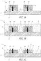
- FIGS. 1A-1Gare schematic side cross-sectional views of various stages of a direct bonding process, according to one embodiment.
- FIG. 1E ′is another example of FIG. 1E according to one embodiment.
- FIG. 1F ′is another example of FIG. 1F according to one embodiment.
- FIGS. 2A-2Eare schematic side cross-sectional views of various stages of a direct bonding process, according to another embodiment.
- FIGS. 3A-3Cillustrate various stages of a direct gang bonding process in which elements are directly bonded to one another without intervening adhesives.
- FIGS. 4A-4Dillustrate examples of bonded structures according to various embodiments.
- FIG. 5Aillustrates schematic side cross-sectional views of a bonded structure according to various embodiments.
- FIGS. 5B-5Dillustrate enlarged views of a portion of the bonded structure of FIG. 5A .
- FIG. 6is a schematic diagram of a system incorporating one or more bonded structures according to various embodiments.
- Some methods of stacking integrated device diescan mount multiple first dies to a tape structure and stack second dies onto the first dies that are disposed on the tape structure.
- the use of a tape structure to support the first diesmay inadequately secure the first dies to the tape structure.
- the stacked diescan be overmolded or otherwise processed into a reconstituted wafer for subsequent processing. Overmolding or other steps in the reconstitution process may induce stresses on the integrated device dies, may be costly, and/or may utilize a thick layer of low coefficient of thermal expansion (CTE) material which may be difficult to manufacture. Accordingly, there remains a continuing need for improved stacking of elements such as integrated device dies.
- CTEcoefficient of thermal expansion
- a first plurality of elementscan be simultaneously directly bonded to a second plurality of elements without intervening adhesives.
- adjacent elements on a carrierPrior to and during direct bonding, adjacent elements on a carrier may be spaced apart by a gap that is not filled with a filling material. The lack of a filling material during direct bonding can reduce thermal stresses that may occur if a filling material were used between adjacent elements and can also simplify the deposition process.
- a dielectric layercan be conformally deposited over upper and side surfaces of the elements. After bonding, outer side surfaces of the dielectric layers of two bonded elements may be laterally offset relative to one another.
- FIGS. 1A-1Gare schematic side cross-sectional views of various stages of a method for preparing elements 3 a , 3 b for forming a bonded structure 1 , according to one embodiment.
- a first plurality of elements 3 a , 3 bcan be mounted to an upper surface 8 of a carrier 2 .
- the elements 3 a , 3 bcan be directly bonded to the upper surface 8 of the carrier 2 without an intervening adhesive.
- the carrier 2can comprise for example, a substrate (e.g., a semiconductor substrate), an interposer, a wafer, a reconstituted wafer, or any other suitable type of carrier.
- the carrier 2can comprise a silicon substrate (e.g., part or all of a wafer), a glass substrate, or silicon on insulator (SOI) substrate or planar dielectric surface 8 .
- a silicon substratee.g., part or all of a wafer
- SOIsilicon on insulator
- the use of silicon, glass, or other semiconductor material for the carrier 2can advantageously enable the upper surface 8 of the carrier 2 to be polished to a very low surface roughness so that the first elements 3 a , 3 b can be directly bonded to the carrier 2 .
- the carrier 2can comprise a silicon carrier with a dielectric surface, for example, an oxide layer formed on the upper surface 8 .
- the dielectric surface or the oxide layercan be formed in any suitable manner, for example, by thermal oxidation, Plasma Enhanced Chemical Vapor Deposition (PECVD), chemical oxidation, sputtering, evaporation, atomic layer deposition (ALD), etc.
- PECVDPlasma Enhanced Chemical Vapor Deposition
- ALDatomic layer deposition
- the elements 3 a , 3 bcan comprise any suitable type of element, such as a semiconductor element.
- the elements 3 a , 3 bcan comprise integrated device dies (e.g., integrated circuit, dies, memory dies, microelectromechanical systems dies, sensor dies, etc.).
- the elements 3 a , 3 bcan include an active surface or region 6 that is patterned with active devices, such as electronic devices like transistors.
- One or a plurality of interconnects or vias 10can extend through a portion of the elements 3 a , 3 b shown in FIG. 1A . In the step of FIG.
- the vias 10can extend from a bottom surface 5 of the active region 6 into a bulk portion 4 (e.g., bulk silicon portion) of the elements 3 a , 3 b .
- the vias 10can be connected to contact pads on the bottom surface 5 of the elements 3 a , 3 b that are directly bonded to corresponding contact or bond pads on the upper surface 8 of the carrier 2 .
- the elements 3 a , 3 bmay comprise the same type of element or different types of elements in various embodiments.
- the bonding surfaces of the elements 3 a , 3 b and the carrier 2can be prepared for bonding.
- the elements 3 a , 3 bcan be polished to a very high degree of smoothness (e.g., less than 20 nm surface roughness, less than 1 nm surface roughness, or more particularly, less than 0.5 nm roughness).
- a bonding layer(not shown) (e.g., a dielectric such as silicon oxide) may be deposited on the active surfaces 6 of the elements 3 a , 3 b and polished to a very high degree of smoothness.
- the bonding surface of the carrier 2may be polished to a very high degree of smoothness (e.g., less than 20 nm surface roughness, less than 1 nm surface roughness, or more particularly, less than 0.5 nm roughness).
- the bonding surfacesmay be fluorinated to improve bonding energy or strength between the bonding surface of the carrier 2 and the mating or bonding surfaces of elements 3 a and 3 b .
- the bonding surfacesmay also include conductive features, such as conductive bond or contact pads, conductive traces or conductive dummy features.
- the surfaces to be bondedmay be terminated with a suitable species and activated prior to bonding.
- the surfaces to be bondedmay be very lightly etched for activation and exposed to a nitrogen-containing solution and terminated with a nitrogen-containing species.
- the surfaces to be bondedmay be exposed to an ammonia dip after a very slight etch, and/or a nitrogen-containing plasma (with or without a separate etch).
- nonconductive field regions of the elements 3 a , 3 bcan be brought into contact with corresponding nonconductive field regions of the carrier 2 .
- the interaction of the activated surfacescan cause the nonconductive regions of the elements 3 a , 3 b to directly bond with the corresponding nonconductive regions of the carrier 2 without an intervening adhesive, without application of external pressure, without application of voltage, and about room temperature.
- the bonding strength of the nonconductive regionscan be covalent bonds that are greater than Van der Waals bonds.
- the nonconductive regionsare initially bonded at about room temperature.
- covalent bondingcan occur during a natural anneal at about room temperature or during a heated anneal.
- the interconnects or vias 10 and/or the contact padsare flush or slightly recessed relative to the exterior surfaces of the elements 3 a , 3 b and the carrier 2 .
- one of the interconnects 10 and/or the contact padsmay extend above the exterior surfaces of the elements 3 a , 3 b and the carrier 2 .
- the interconnects 10 and/or the contact padsare recessed relative to the exterior surfaces (e.g., oxide field regions) of the elements 3 a , 3 b and the carrier 2 .
- the recessmay range between 1 to 40 nm.
- the bonded structure 1can be annealed after the nonconductive regions are bonded to create contact and a direct bond between opposing conductive regions (e.g., between opposing contact pads) without an intervening adhesive.
- the bonded structure 1can be annealed after the nonconductive regions are bonded to create contact and a direct bond between opposing conductive regions (e.g., between opposing contact pads) without an intervening adhesive.
- the carrier 2 and elements 3 a , 3 bmay be heated after bonding to strengthen the bonds between the nonconductive regions, between the conductive regions, and/or between opposing conductive and non-conductive regions, to cause the elements 3 a , 3 b to bond with the carrier 2 . Additional details of the direct bonding processes may be found throughout U.S.
- a sacrificial filler material 9can be provided over the elements 3 a , 3 b and the upper surface 8 of the carrier 2 , and filling the space between the elements 3 a , 3 b .
- the sacrificial filler material 9can comprise any suitable type of temporary or sacrificial material that can be removed by way of subsequent processing.
- the sacrificial material 9can comprise a photoresist material, such as a hard baked photoresist, a spin on polymer coating, an adhesive film, polyimide, etc.
- the partially-formed structure 1can be thinned.
- a portion of the sacrificial material 9 and a portion of the elements 3 a , 3 bcan be selectively removed to thin the structure 1 .
- an upper surface of the sacrificial material 9can be grinded, polished, dry etched with a plasma process, or wet etched with a chemical to expose upper sides of the elements 3 a , 3 b .
- grinding and chemical mechanical polishing (CMP)can be used to remove the upper portion of the sacrificial filler material 9 and upper portions of the elements 3 a , 3 b .
- the portions of the upper sides of the elements 3 a , 3 bcan also be removed to expose the interconnects or vias 10 at an exposed upper surface 11 of bulk portions 4 of the elements 3 a , 3 b . As illustrated in FIG. 1C , a portion of the interconnects 10 can protrude from a surface of the bulk portions 4 .
- the sacrificial filler material 9may facilitate planarization of the exposed surfaces 11 of the elements 3 a , 3 b while reducing stresses on the corners of elements 3 a , 3 b.
- the sacrificial filler material 9can be removed such that no filler material is disposed over or between the elements 3 a , 3 b .
- the sacrificial filler material 9can be removed by a wet or dry etching process, a plasma etching process, a stripping process, etc.
- the upper corners or edges between the horizontal and vertical portions of element 3 a and 3 bmay crack or chip off if gentle pressures are not utilized during the thinning and polishing of the backsides of element 3 a and 3 b .
- the elements 3 a , 3 bcan be separated by a gap 7 .
- the gap 7may not include a filling material, for example, the gap 7 may be filled with a gas (such as air) or may be under vacuum.
- a dielectric material comprising a dielectric layer 12can be deposited over the elements 3 a , 3 b and over portions of the upper surface 8 of the carrier 2 disposed between adjacent elements 3 a , 3 b .
- the dielectric layer 12may comprise a conformal dielectric coating, as illustrated in FIG. 1E ′.
- a portion of the dielectric layer 12 above the protruded via 10can be higher than area surrounding the portion.
- the thickness of the dielectric layer 12is smaller than the thickness of elements 3 a or 3 b .
- the dielectric layer 12can serve as a protective material to protect the upper and side surfaces of the elements 3 a , 3 b .
- the dielectric layer 12can also be selected to serve as a nonconductive bonding layer or region for subsequent direct bonding steps.
- the dielectric layer 12can comprise any suitable type of dielectric material.
- the dielectric layer 12can comprise silicon oxide, silicon nitride, silicon oxynitride, silicon carbide, or any other suitable dielectric.
- the dielectric layer 12may comprise multiple layers of different dielectric materials.
- the dielectric layer 12can cover debris or cracks weakly bonded due to die singulation and which might negatively impact the bond. As shown the gap 7 can be disposed between portions of the dielectric layer 12 disposed on sidewalls of adjacent elements 3 a , 3 b.
- a second sacrificial filler material 13can be provided over the dielectric layer 12 including the gaps 7 in FIG. 1F .
- the second sacrificial layer 13may comprise a dielectric coating, as illustrated in FIG. 1F ′.
- the second sacrificial filler material 13can facilitate thinning of the partially-formed bonded structure 1 .
- the partially-formed bonded structure 1can be thinned.
- an upper portion of the second sacrificial filler material 13 and upper portions of the dielectric layer 12can be selectively removed, for example, by polishing, grinding, etc.
- the second sacrificial material 13can be then completely removed. As shown in FIG. 1G , only a portion of the dielectric layer 12 can be removed, so as to expose the vias 10 at an exposed upper portion 14 of the dielectric layer 12 .
- FIGS. 2A-2Eare schematic side cross-sectional views of various stages of a method for forming a preliminary bonded structure 1 , according to another embodiment. Unless otherwise noted, the components of FIGS. 2A-2E may be the same as or generally similar to like-numbered components of FIGS. 1A-1G .
- a carrier 2can be provided in FIG. 2A .
- elements 3 a , 3 bcan be directly bonded to the carrier 2 without an intervening adhesive.
- the preliminary bonded structure 1can be thinned, for example, upper surfaces of the elements 3 a , 3 b , for example the bulk portion 4 , can be selectively removed (e.g., by grinding, polishing, dry etched with a plasma process, or wet etched with a chemical) without providing a sacrificial filler material over and between the elements 3 a , 3 b .
- the elements 3 a , 3 bcan be planarized to expose the vias 10 at exposed surface 11 without using a sacrificial filler material.
- a portion of the vias 10can protrude from the exposed surface 11 .
- FIG. 2Ca portion of the vias 10 can protrude from the exposed surface 11 .
- the dielectric layer 12can be provided over the elements 3 a , 3 b in FIG. 2D .
- An upper portion of the dielectric layer 12can be removed (for example, by polishing, grinding, etc.) to expose the vias 10 at the exposed upper portion 14 of the dielectric layer 12 .
- a gap 7may be provided between the elements 3 a , 3 b as shown in FIG. 2E .
- FIGS. 3A-3Cillustrate various stages of a direct gang bonding process in which a first plurality of elements 3 a , 3 b is direct bonded to a corresponding second plurality of elements 3 a ′, 3 b ′ without intervening adhesives.
- the bonding process illustrated in FIGS. 3A-3Ccan be used for a wafer to wafer bonding process, in which each wafer includes numerous elements to be directly bonded.
- components of FIGS. 3A-3Cmay be the same as or generally similar to like-numbered components of FIGS. 1A-2D . For example, in FIG.
- the exposed upper surfaces 14 , 14 ′ of the dielectric layers 12 , 12 ′ of the elements 3 a , 3 b , 3 a ′, 3 b ′can be prepared for direct bonding as explained above in connection with FIG. 1A .
- the processes described in connection with FIGS. 1G and 2Emay be used to at least partially prepare the surfaces of the dielectric layer 12 for bonding. Additional processing may be performed to prepare the dielectric layer 12 and the contact pads connected to the exposed portion of the vias 10 for direct bonding.
- the surfaces 14 , 14 ′ to be bondedmay be very lightly etched for activation and exposed to a nitrogen-containing solution and terminated with a nitrogen-containing species.
- a pre-process for direct bondingmay be performed.
- the pre-processmay include a surface cleaning process such as a vacuum ultraviolet irradiation, a vacuum ultraviolet/ozone irradiation, sulfuric-peroxide mixture (SPM) cleaning process, etc.
- the elements 3 a ′ and 3 b ′may be simultaneously brought into direct contact with the elements 3 a , 3 b .
- the surfaces 14 , 14 ′are prepared, nonconductive field regions of the elements 3 a , 3 b can be brought into contact with each other.
- the interaction of the activated surfacescan cause the nonconductive regions of the elements 3 a , 3 b to directly bond with the corresponding nonconductive regions of the elements 3 a , 3 b without an intervening adhesive, without application of external pressure, without application of voltage, and about room temperature.
- the bonding strength of the nonconductive regionscan be covalent bonds that are greater than Van der Waals bonds.
- covalent bondingcan occur between the surfaces 14 , 14 ′.
- the bonded structure 1can be annealed after directly bonding the surfaces 14 , 14 ′.
- the structure of FIG. 3Bcan be annealed at elevated temperature to enhance the bond strength of the non-conductive area around via 10 and to form direct metal-to-metal bonding of the vias 10 (or contact pads connected to the vias 10 ).
- the element 3 a ′can be directly bonded to the element 3 a along a bond interface 15 without an intervening adhesive.
- the element 3 b ′can be directly bonded to the element 3 b along a bond interface 15 without an intervening adhesive.
- the same or a generally similar method of directly bonding the elements 3 a , 3 b and the carrier 2can be used for bonding the elements 3 a ′, 3 b ′ and the elements 3 a , 3 b , respectively.
- the elements 3 a , 3 bmay occlude the gap 7 in which no filling material is disposed. Rather, as shown in FIGS. 3A-3B , the gap 7 may be filled with a gas (such as air) or under vacuum.
- a gassuch as air
- the absence of filling material during bondingcan reduce stresses on the elements 3 a , 3 b that may be introduced during heating due to different coefficients of thermal expansion (CTE) of the filling material(s) and may reduce the number of process steps, thus lowering fabrication costs.
- CTEcoefficients of thermal expansion
- the carrier 2 ′ to which the elements 3 a ′, 3 b ′ are bondedmay be removed.
- the elements 3 a , 3 a ′ and 3 b , 3 b ′may be slightly laterally offset relative to one another, due to, for example, inaccuracies in the alignment process.
- the carrier 2 ′can be removed in any suitable manner, for example, by etching, grinding, polishing, etc.
- the carrier 2 to which the elements 3 a , 3 b are bondedmay also be removed. As shown in FIG.
- the dielectric layer 12 ′ on the element 3 a ′can define a first outer surface 17 a
- the dielectric layer 12 on the element 3 bcan define a second outer surface 17 b
- the bonded structure 1 of FIG. 3Ccan be integrated into the larger electronic system, for example, by mounting the bonded structure 1 to a system or motherboard. In some embodiments, therefore, the first and second outer surfaces 17 a , 17 b can be exposed on an exterior surface of the bonded structure 1 .
- an overhanging portion 13 ′ of the dielectric layer 12 ′can remain after the removal of the carrier 2 ′, and can overhang the bonded structure.
- the overhanging portion of the dielectric layer 12may break off during subsequent processing.
- FIGS. 4A-4Dillustrate examples of bonded structures 1 during various stages of a stacking process.
- components of FIGS. 4A-4Dmay be the same as or generally similar to like-numbered components of FIGS. 1A-3C .
- the same or a generally similar method of directly bonding the elements 3 a , 3 b associated with FIGS. 1A-3Ccan be used.
- the gap 7 between the elements 3 a , 3 a ′, 3 b , 3 b ′ produced in FIG. 3Ccan be filled with a filling material 16 , such as a molding compound.
- the filling material 16can protect the elements 3 a , 3 a ′, 3 b , 3 b ′ during a subsequent process or during operation.
- the filling material 16can be applied within the gaps disposed between adjacent stacked structures.
- the filling material 16can be applied in a flowable form, and can be hardened by/after curing.
- the filling material 16can be applied after the elements 3 a , 3 a ′ and the elements 3 b , 3 b ′ are direct bonded, such that the filling material 16 can comprise a seamless filler.
- the filling material 16can comprise a single layer of filler. In other embodiments, however, no filling material can be applied, and the bonded structure 1 of FIG. 3C can be integrated into the larger electronic system.
- the bonded structure 1 of FIG. 4Acan be singulated along saw lines between the elements 3 a , 3 b and between the elements 3 a ′, 3 b ′ to form a singulated bonded structure 1 .
- the filling material 16can be disposed along the side surfaces of the singulated bonded structure 1 .
- the filling material 16can comprise markings indicative of a sawing process or other methods such as laser stealth dicing or laser ablation used during singulation.
- the carrier 2may remain bonded to the elements 3 a , 3 b for integration into the larger electronic system or device in some embodiments.
- the carrier 2can be bonded (e.g., direct bonded or adhered with an adhesive such as solder) to a motherboard of the larger electronic system.
- the carrier 2can be removed such that the elements 3 a , 3 b and/or 3 a ′, 3 b ′ can be bonded to the motherboard of the larger electronic system.
- FIG. 4Dillustrates a bonded structure 1 in which more than two elements are bonded together to form a stacked bonded structure.
- element 3 a ′′can be directly bonded to element 3 a ′
- element 3 a ′′′can be directly bonded to element 3 a ′′.
- the interconnects or vias 10can provide vertical electrical communication among the elements 3 a - 3 a ′′′.
- four elements 3 a - 3 a ′′′are shown in FIG. 4D , in other embodiments, more or fewer than four elements can be provided. In the embodiment of FIG.
- the outer side surfaces defined at least in part by the dielectric layers 12 , 12 ′, 12 ′′, 12 ′′′can be exposed on the exterior surface of the bonded structure 1 .
- a filling materialcan be provided between the bonded structures such that, in FIG. 4D , the filling material can be disposed alongside surfaces of the dielectric layers 12 , 12 ′, 12 ′′, 12 ′′′.
- FIG. 5Aillustrates a bonded structure 1 prior to singulation.
- FIGS. 5B-5Dillustrate magnified portions of the bonded structure 1 of FIG. 5A .
- components of FIGS. 5A-5Dmay be the same as or generally similar to like-numbered components of FIGS. 1A-4D .
- one or both carriers 2 , 2 ′can be removed from the bonded structure.
- the carrier(s) 2 and/or 2 ′can be removed by etching, grinding, polishing, or any other suitable removal method.
- a portion of the dielectric layer 12 ′can fracture or break away from the carrier 2 ′.
- the breaking away of the carrier 2 ′ from the dielectric layer 12 ′can form a fractured surface (or structure) 18 a or 18 b in the dielectric layer 12 ′.
- the fractured surface 18 acan comprise a concave surface in which a portion of the dielectric material 12 ′ along side surfaces 20 of the element 3 a ′ is removed.
- a fractured surface 18 bcan comprise a concave surface or projection that extends outwardly from the side of the bonded structure 1 .
- the fractured surface (or structure) 18 a or 18 bcan be disposed at a portion of the dielectric layer 12 ′ at or near a surface of the element 3 a ′ opposite the bonding interface 15 between the elements 3 a , 3 a ′.
- an interface where the element 3 a ′ and the dielectric layer 12 ′ meetcan fracture or break away from the carrier 2 ′ (not illustrated).
- portions dielectric layer 12 ′ abutting carrier 2 ′may be selectively removed (not illustrated) prior to the bond of the horizontal surface of elements 3 a and 3 b to the respective counterparts 3 a ′ and 3 b ′. The selective removal of selected portions of dielectric layer 12 ′ from the surface of carrier 2 ′ reduces the incidence of fractures of FIGS. 5B and 5C during the removal of carrier 2 ′.
- the dielectric layers 12 , 12 ′can coat (e.g., conformally coat in some embodiments) side surfaces 20 of the elements 3 a , 3 a ′ and the exposed upper surfaces 11 , 11 ′ of the respective elements 3 a , 3 a ′.
- upper portions 12 a ′ of the dielectric layers 12 ′can be provided over the exposed upper surfaces 11 , 11 ′ of the respective elements 3 a , 3 a ′.
- the upper portion 12 a of the dielectric layer 12 on the element 3 acan be directly bonded without an intervening adhesive to the corresponding upper portion 12 a ′ of the dielectric layer 12 ′ on the element 3 a ′.
- the dielectric layers 12 , 12 ′can be rounded or curved along curved surfaces 19 , 19 ′ that are disposed between the side surfaces 20 , 20 ′ and the upper surfaces 11 , 11 ′ of the elements 3 a , 3 a ′.
- the first dielectric layers 12 , 12 ′is curved along an edge or corner of the first and the second element 3 a , 3 a ′ between the first and second bonding surfaces and the at least one first and second side surface.
- the elements 3 a , 3 a ′may be slightly misaligned such that, after direct bonding, side surfaces 20 , 20 ′ of the elements 3 a , 3 a ′ and outer surfaces 17 a , 17 b of the dielectric layers 12 , 12 ′ are laterally offset relative to one another by an offset distance d.
- the offset distance dcan be less than 2 ⁇ m, less than 5 ⁇ m, or less than 10 ⁇ m, for example, in a range of 0.2 ⁇ m to 10 ⁇ m, in a range of 0.2 ⁇ m to 5 ⁇ m, in a range of 0.2 ⁇ m to 2 ⁇ m, or in a range of 0.2 ⁇ m to 1 ⁇ m.
- the offset distance dcan be less than the width of the via 10 or other contact pads which are connected to one another (which as explained above can result from misalignment between the top and bottom elements or dies). In various embodiments, for example, the offset distance d can be substantially smaller than a width of the contact pads or vias 10 . For example, the offset distance d can be less than 95% of the width of contact pads or vias 10 , or less than 60% of the width of contact pads or vias 10 . The offset distance d may be sufficiently small such that contact pads connected to the interconnects 10 maintain direct contact after bonding. In some embodiment, the offset distance d is less than 5% of the thickness of the elements 3 a or 3 b , for example, less than 10% of the thickness of the elements 3 a , 3 b.
- FIG. 6is a schematic diagram of a system 80 incorporating one or more bonded structures 1 , according to various embodiments.
- the system 80can comprise any suitable type of electronic device, such as a mobile electronic device (e.g., a smartphone, a tablet computing device, a laptop computer, etc.), a desktop computer, an automobile or components thereof, a stereo system, a medical device, a camera, or any other suitable type of system.
- the electronic devicecan comprise a microprocessor, a graphics processor, an electronic recording device, or digital memory.
- the system 80can include one or more device packages 82 which are mechanically and electrically connected to the system 80 , e.g., by way of one or more motherboards. Each package 82 can comprise one or more bonded structures 1 .
- the bonded structures 1 shown in FIG. 6can comprise any of the bonded structures 1 shown and described above in connection with FIGS. 1A-5D .
- the bonded structure 1can include one or more integrated device dies which perform various functions for the system 80
Landscapes
- Engineering & Computer Science (AREA)
- Microelectronics & Electronic Packaging (AREA)
- Power Engineering (AREA)
- Computer Hardware Design (AREA)
- Physics & Mathematics (AREA)
- Condensed Matter Physics & Semiconductors (AREA)
- General Physics & Mathematics (AREA)
- Manufacturing & Machinery (AREA)
- Wire Bonding (AREA)
- Micromachines (AREA)
Abstract
Description
- This application claims priority to U.S. Provisional Patent Application No. 62/906,608, filed Sep. 26, 2019, the entire contents of which are incorporated by reference in their entirety and for all purposes.
- The field relates to direct gang bonding methods and structures.
- In various packaging arrangements, it can be advantageous to enable the use of multiple integrated device dies within a low-profile package. For example, three-dimensional (3D) integration techniques often utilize packages in which two or more integrated device dies are stacked on top of and electrically connected to one another. Conventional methods for die thinning and/or 3D integration may have limited product yield because stresses imparted to the dies during assembly may damage dies in the stack. Moreover, it can be challenging to stack dies which have different thicknesses and which have high pin counts and which may originate from different types of substrates and/or wafers. Accordingly, there remains a continuing need for improved systems and methods for stacking integrated device dies.
- These aspects and others will be apparent from the following description of preferred embodiments and the accompanying drawing, which is meant to illustrate and not to limit the invention, wherein:
FIGS. 1A-1G are schematic side cross-sectional views of various stages of a direct bonding process, according to one embodiment.FIG. 1E ′ is another example ofFIG. 1E according to one embodiment.FIG. 1F ′ is another example ofFIG. 1F according to one embodiment.FIGS. 2A-2E are schematic side cross-sectional views of various stages of a direct bonding process, according to another embodiment.FIGS. 3A-3C illustrate various stages of a direct gang bonding process in which elements are directly bonded to one another without intervening adhesives.FIGS. 4A-4D illustrate examples of bonded structures according to various embodiments.FIG. 5A illustrates schematic side cross-sectional views of a bonded structure according to various embodiments.FIGS. 5B-5D illustrate enlarged views of a portion of the bonded structure ofFIG. 5A .FIG. 6 is a schematic diagram of a system incorporating one or more bonded structures according to various embodiments.- Some methods of stacking integrated device dies can mount multiple first dies to a tape structure and stack second dies onto the first dies that are disposed on the tape structure. However, the use of a tape structure to support the first dies may inadequately secure the first dies to the tape structure. Moreover, in some methods, the stacked dies can be overmolded or otherwise processed into a reconstituted wafer for subsequent processing. Overmolding or other steps in the reconstitution process may induce stresses on the integrated device dies, may be costly, and/or may utilize a thick layer of low coefficient of thermal expansion (CTE) material which may be difficult to manufacture. Accordingly, there remains a continuing need for improved stacking of elements such as integrated device dies.
- Various embodiments disclosed herein relate to direct gang bonding methods and structures. For example, in various embodiments, a first plurality of elements can be simultaneously directly bonded to a second plurality of elements without intervening adhesives. Prior to and during direct bonding, adjacent elements on a carrier may be spaced apart by a gap that is not filled with a filling material. The lack of a filling material during direct bonding can reduce thermal stresses that may occur if a filling material were used between adjacent elements and can also simplify the deposition process. In various embodiments, a dielectric layer can be conformally deposited over upper and side surfaces of the elements. After bonding, outer side surfaces of the dielectric layers of two bonded elements may be laterally offset relative to one another.
FIGS. 1A-1G are schematic side cross-sectional views of various stages of a method for preparingelements structure 1, according to one embodiment. InFIG. 1A , a first plurality ofelements upper surface 8 of acarrier 2. In the illustrated embodiment, theelements upper surface 8 of thecarrier 2 without an intervening adhesive. Thecarrier 2 can comprise for example, a substrate (e.g., a semiconductor substrate), an interposer, a wafer, a reconstituted wafer, or any other suitable type of carrier. In some embodiments, thecarrier 2 can comprise a silicon substrate (e.g., part or all of a wafer), a glass substrate, or silicon on insulator (SOI) substrate or planardielectric surface 8. The use of silicon, glass, or other semiconductor material for thecarrier 2 can advantageously enable theupper surface 8 of thecarrier 2 to be polished to a very low surface roughness so that thefirst elements carrier 2. In the illustrated embodiment, for example, thecarrier 2 can comprise a silicon carrier with a dielectric surface, for example, an oxide layer formed on theupper surface 8. The dielectric surface or the oxide layer can be formed in any suitable manner, for example, by thermal oxidation, Plasma Enhanced Chemical Vapor Deposition (PECVD), chemical oxidation, sputtering, evaporation, atomic layer deposition (ALD), etc.- The
elements elements elements region 6 that is patterned with active devices, such as electronic devices like transistors. One or a plurality of interconnects orvias 10 can extend through a portion of theelements FIG. 1A . In the step ofFIG. 1A , thevias 10 can extend from abottom surface 5 of theactive region 6 into a bulk portion4 (e.g., bulk silicon portion) of theelements vias 10 can be connected to contact pads on thebottom surface 5 of theelements upper surface 8 of thecarrier 2. Theelements - To accomplish the direct bonding, in some embodiments, the bonding surfaces of the
elements carrier 2 can be prepared for bonding. Theelements active surfaces 6 of theelements upper surface 8 of the carrier2) may be polished to a very high degree of smoothness (e.g., less than 20 nm surface roughness, less than 1 nm surface roughness, or more particularly, less than 0.5 nm roughness). In some embodiments, the bonding surfaces may be fluorinated to improve bonding energy or strength between the bonding surface of thecarrier 2 and the mating or bonding surfaces ofelements - Once the surfaces are prepared, nonconductive field regions of the
elements carrier 2. The interaction of the activated surfaces can cause the nonconductive regions of theelements carrier 2 without an intervening adhesive, without application of external pressure, without application of voltage, and about room temperature. In various embodiments, the bonding strength of the nonconductive regions can be covalent bonds that are greater than Van der Waals bonds. In various embodiments, the nonconductive regions are initially bonded at about room temperature. In some embodiments, covalent bonding can occur during a natural anneal at about room temperature or during a heated anneal. In some embodiments, the interconnects orvias 10 and/or the contact pads are flush or slightly recessed relative to the exterior surfaces of theelements carrier 2. In other embodiments, one of theinterconnects 10 and/or the contact pads may extend above the exterior surfaces of theelements carrier 2. In still other embodiments, theinterconnects 10 and/or the contact pads are recessed relative to the exterior surfaces (e.g., oxide field regions) of theelements carrier 2. Depending on the depth and width of the conductive features10, the recess may range between 1 to 40 nm. The bondedstructure 1 can be annealed after the nonconductive regions are bonded to create contact and a direct bond between opposing conductive regions (e.g., between opposing contact pads) without an intervening adhesive. The bondedstructure 1 can be annealed after the nonconductive regions are bonded to create contact and a direct bond between opposing conductive regions (e.g., between opposing contact pads) without an intervening adhesive. In various embodiments, thecarrier 2 andelements elements carrier 2. Additional details of the direct bonding processes may be found throughout U.S. Pat. Nos. 7,126,212; 8,153,505; 7,622,324; 7,602,070; 8,163,373; 8,389,378; 8,735,219; 9,953,941; and 10,204,893, and throughout U.S. Patent Publication No. US 2017/0200711, the contents of each of which are hereby incorporated by reference herein in their entirety and for all purposes. - Turning to
FIG. 1B , asacrificial filler material 9 can be provided over theelements upper surface 8 of thecarrier 2, and filling the space between theelements sacrificial filler material 9 can comprise any suitable type of temporary or sacrificial material that can be removed by way of subsequent processing. For example, in various embodiments, thesacrificial material 9 can comprise a photoresist material, such as a hard baked photoresist, a spin on polymer coating, an adhesive film, polyimide, etc. InFIG. 1C , the partially-formedstructure 1 can be thinned. For example, a portion of thesacrificial material 9 and a portion of theelements structure 1. For example, an upper surface of thesacrificial material 9 can be grinded, polished, dry etched with a plasma process, or wet etched with a chemical to expose upper sides of theelements sacrificial filler material 9 and upper portions of theelements elements vias 10 at an exposedupper surface 11 ofbulk portions 4 of theelements FIG. 1C , a portion of theinterconnects 10 can protrude from a surface of thebulk portions 4. In some arrangements, thesacrificial filler material 9 may facilitate planarization of the exposed surfaces11 of theelements elements - In
FIG. 1D , thesacrificial filler material 9 can be removed such that no filler material is disposed over or between theelements sacrificial filler material 9 can be removed by a wet or dry etching process, a plasma etching process, a stripping process, etc. In arrangements in which there is no sacrificial material, the upper corners or edges between the horizontal and vertical portions ofelement element FIG. 1D , theelements gap 7. Thegap 7 may not include a filling material, for example, thegap 7 may be filled with a gas (such as air) or may be under vacuum. Turning toFIG. 1E , a dielectric material comprising adielectric layer 12 can be deposited over theelements upper surface 8 of thecarrier 2 disposed betweenadjacent elements dielectric layer 12 may comprise a conformal dielectric coating, as illustrated inFIG. 1E ′. For example, a portion of thedielectric layer 12 above the protruded via10 can be higher than area surrounding the portion. In some applications, the thickness of thedielectric layer 12 is smaller than the thickness ofelements dielectric layer 12 can serve as a protective material to protect the upper and side surfaces of theelements dielectric layer 12 can also be selected to serve as a nonconductive bonding layer or region for subsequent direct bonding steps. Thedielectric layer 12 can comprise any suitable type of dielectric material. For example, in various embodiments, thedielectric layer 12 can comprise silicon oxide, silicon nitride, silicon oxynitride, silicon carbide, or any other suitable dielectric. In some embodiments, thedielectric layer 12 may comprise multiple layers of different dielectric materials. At the edge of the die, thedielectric layer 12 can cover debris or cracks weakly bonded due to die singulation and which might negatively impact the bond. As shown thegap 7 can be disposed between portions of thedielectric layer 12 disposed on sidewalls ofadjacent elements - A second
sacrificial filler material 13 can be provided over thedielectric layer 12 including thegaps 7 inFIG. 1F . In some embodiments, the secondsacrificial layer 13 may comprise a dielectric coating, as illustrated inFIG. 1F ′. As with thesacrificial filler material 9, the secondsacrificial filler material 13 can facilitate thinning of the partially-formed bondedstructure 1. Turning toFIG. 1G , the partially-formed bondedstructure 1 can be thinned. For example, an upper portion of the secondsacrificial filler material 13 and upper portions of thedielectric layer 12 can be selectively removed, for example, by polishing, grinding, etc. In some embodiments, the secondsacrificial material 13 can be then completely removed. As shown inFIG. 1G , only a portion of thedielectric layer 12 can be removed, so as to expose thevias 10 at an exposedupper portion 14 of thedielectric layer 12. FIGS. 2A-2E are schematic side cross-sectional views of various stages of a method for forming a preliminary bondedstructure 1, according to another embodiment. Unless otherwise noted, the components ofFIGS. 2A-2E may be the same as or generally similar to like-numbered components ofFIGS. 1A-1G . InFIG. 2A , acarrier 2 can be provided. As shown inFIG. 2B , as withFIG. 1A ,elements carrier 2 without an intervening adhesive. Moving toFIG. 2C , the preliminary bondedstructure 1 can be thinned, for example, upper surfaces of theelements bulk portion 4, can be selectively removed (e.g., by grinding, polishing, dry etched with a plasma process, or wet etched with a chemical) without providing a sacrificial filler material over and between theelements elements vias 10 at exposedsurface 11 without using a sacrificial filler material. As illustrated inFIG. 2C , a portion of the vias10 can protrude from the exposedsurface 11. As withFIG. 1E or 1E ′, thedielectric layer 12 can be provided over theelements FIG. 2D . An upper portion of thedielectric layer 12 can be removed (for example, by polishing, grinding, etc.) to expose thevias 10 at the exposedupper portion 14 of thedielectric layer 12. As with the embodiment ofFIGS. 1A-1G , once the vias10 are exposed, agap 7 may be provided between theelements FIG. 2E .FIGS. 3A-3C illustrate various stages of a direct gang bonding process in which a first plurality ofelements elements 3a′,3b′ without intervening adhesives. In some embodiments, the bonding process illustrated inFIGS. 3A-3C can be used for a wafer to wafer bonding process, in which each wafer includes numerous elements to be directly bonded. Unless otherwise noted, components ofFIGS. 3A-3C may be the same as or generally similar to like-numbered components ofFIGS. 1A-2D . For example, inFIG. 3A , the exposedupper surfaces dielectric layers elements FIG. 1A . In various embodiments, the processes described in connection withFIGS. 1G and 2E may be used to at least partially prepare the surfaces of thedielectric layer 12 for bonding. Additional processing may be performed to prepare thedielectric layer 12 and the contact pads connected to the exposed portion of thevias 10 for direct bonding. For example, in some embodiments, thesurfaces surfaces - In
FIG. 3B , theelements 3a′ and3b′ may be simultaneously brought into direct contact with theelements surfaces elements elements elements surfaces structure 1 can be annealed after directly bonding thesurfaces - In some embodiments, the structure of
FIG. 3B can be annealed at elevated temperature to enhance the bond strength of the non-conductive area around via10 and to form direct metal-to-metal bonding of the vias10 (or contact pads connected to the vias10). Thus, inFIG. 3B , theelement 3a′ can be directly bonded to theelement 3aalong abond interface 15 without an intervening adhesive. Theelement 3b′ can be directly bonded to theelement 3balong abond interface 15 without an intervening adhesive. In some embodiments, the same or a generally similar method of directly bonding theelements carrier 2 can be used for bonding theelements 3a′,3b′ and theelements - As shown, prior to and during direct bonding of the
elements elements elements 3a′,3b′) may occlude thegap 7 in which no filling material is disposed. Rather, as shown inFIGS. 3A-3B , thegap 7 may be filled with a gas (such as air) or under vacuum. Beneficially, the absence of filling material during bonding can reduce stresses on theelements - Turning to
FIG. 3C , thecarrier 2′ to which theelements 3a′,3b′ are bonded may be removed. As shown inFIG. 3C , theelements carrier 2′ can be removed in any suitable manner, for example, by etching, grinding, polishing, etc. In some embodiments, thecarrier 2 to which theelements FIG. 3C , thedielectric layer 12′ on theelement 3a′ can define a firstouter surface 17a, and thedielectric layer 12 on theelement 3bcan define a secondouter surface 17b. In some embodiments, the bondedstructure 1 ofFIG. 3C can be integrated into the larger electronic system, for example, by mounting the bondedstructure 1 to a system or motherboard. In some embodiments, therefore, the first and secondouter surfaces structure 1. As shown inFIG. 3C , an overhangingportion 13′ of thedielectric layer 12′ can remain after the removal of thecarrier 2′, and can overhang the bonded structure. As shown inFIGS. 5B-5C , the overhanging portion of thedielectric layer 12 may break off during subsequent processing. FIGS. 4A-4D illustrate examples of bondedstructures 1 during various stages of a stacking process. Unless otherwise noted, components ofFIGS. 4A-4D may be the same as or generally similar to like-numbered components ofFIGS. 1A-3C . In some embodiments, the same or a generally similar method of directly bonding theelements FIGS. 1A-3C can be used. InFIG. 4A , for example, thegap 7 between theelements FIG. 3C can be filled with a fillingmaterial 16, such as a molding compound. The fillingmaterial 16 can protect theelements material 16 can be applied within the gaps disposed between adjacent stacked structures. For example, the fillingmaterial 16 can be applied in a flowable form, and can be hardened by/after curing. The fillingmaterial 16 can be applied after theelements elements material 16 can comprise a seamless filler. For example, the fillingmaterial 16 can comprise a single layer of filler. In other embodiments, however, no filling material can be applied, and the bondedstructure 1 ofFIG. 3C can be integrated into the larger electronic system.- As shown in
FIG. 4B , the bondedstructure 1 ofFIG. 4A can be singulated along saw lines between theelements elements 3a′,3b′ to form a singulated bondedstructure 1. Thus, in the singulated bondedstructure 1 ofFIG. 4B , the fillingmaterial 16 can be disposed along the side surfaces of the singulated bondedstructure 1. The fillingmaterial 16 can comprise markings indicative of a sawing process or other methods such as laser stealth dicing or laser ablation used during singulation. Thecarrier 2 may remain bonded to theelements carrier 2 can be bonded (e.g., direct bonded or adhered with an adhesive such as solder) to a motherboard of the larger electronic system. In other embodiments, as shown inFIG. 4C , thecarrier 2 can be removed such that theelements FIG. 4D illustrates a bondedstructure 1 in which more than two elements are bonded together to form a stacked bonded structure. For example, inFIG. 4D ,element 3a″ can be directly bonded toelement 3a′, andelement 3a′″ can be directly bonded toelement 3a″. The interconnects orvias 10 can provide vertical electrical communication among the elements3a-3a′″. Although four elements3a-3a′″ are shown inFIG. 4D , in other embodiments, more or fewer than four elements can be provided. In the embodiment ofFIG. 4D , the outer side surfaces defined at least in part by thedielectric layers structure 1. In other embodiments, as withFIGS. 4A-4C , a filling material can be provided between the bonded structures such that, inFIG. 4D , the filling material can be disposed alongside surfaces of thedielectric layers FIG. 5A illustrates a bondedstructure 1 prior to singulation.FIGS. 5B-5D illustrate magnified portions of the bondedstructure 1 ofFIG. 5A . Unless otherwise noted, components ofFIGS. 5A-5D may be the same as or generally similar to like-numbered components ofFIGS. 1A-4D . As explained above, in various embodiments, one or bothcarriers carrier 2′ is separated from thedielectric layer 12′, a portion of thedielectric layer 12′ can fracture or break away from thecarrier 2′. The breaking away of thecarrier 2′ from thedielectric layer 12′ can form a fractured surface (or structure)18aor18bin thedielectric layer 12′. For example, as shown inFIG. 5B , in some cases, the fractured surface18acan comprise a concave surface in which a portion of thedielectric material 12′ along side surfaces20 of theelement 3a′ is removed. In other cases, as shown inFIG. 5C , a fractured surface18bcan comprise a concave surface or projection that extends outwardly from the side of the bondedstructure 1. As shown inFIGS. 5B and 5C , the fractured surface (or structure)18aor18bcan be disposed at a portion of thedielectric layer 12′ at or near a surface of theelement 3a′ opposite thebonding interface 15 between theelements carrier 2′ is separated from thedielectric layer 12′, an interface where theelement 3a′ and thedielectric layer 12′ meet can fracture or break away from thecarrier 2′ (not illustrated). Still in some embodiments portionsdielectric layer 12′ abuttingcarrier 2′ may be selectively removed (not illustrated) prior to the bond of the horizontal surface ofelements respective counterparts 3a′ and3b′. The selective removal of selected portions ofdielectric layer 12′ from the surface ofcarrier 2′ reduces the incidence of fractures ofFIGS. 5B and 5C during the removal ofcarrier 2′.- Turning to
FIG. 5D , as explained above, thedielectric layers elements upper surfaces respective elements FIG. 5D , upper portions12a′ of thedielectric layers 12′ can be provided over the exposedupper surfaces respective elements dielectric layer 12 on theelement 3acan be directly bonded without an intervening adhesive to the corresponding upper portion12a′ of thedielectric layer 12′ on theelement 3a′. Further, as shown inFIG. 5D , thedielectric layers curved surfaces upper surfaces elements second element elements elements outer surfaces dielectric layers vias 10. For example, the offset distance d can be less than 95% of the width of contact pads orvias 10, or less than 60% of the width of contact pads orvias 10. The offset distance d may be sufficiently small such that contact pads connected to theinterconnects 10 maintain direct contact after bonding. In some embodiment, the offset distance d is less than 5% of the thickness of theelements elements FIG. 6 is a schematic diagram of asystem 80 incorporating one or more bondedstructures 1, according to various embodiments. Thesystem 80 can comprise any suitable type of electronic device, such as a mobile electronic device (e.g., a smartphone, a tablet computing device, a laptop computer, etc.), a desktop computer, an automobile or components thereof, a stereo system, a medical device, a camera, or any other suitable type of system. In some embodiments, the electronic device can comprise a microprocessor, a graphics processor, an electronic recording device, or digital memory. Thesystem 80 can include one or more device packages82 which are mechanically and electrically connected to thesystem 80, e.g., by way of one or more motherboards. Eachpackage 82 can comprise one or more bondedstructures 1. The bondedstructures 1 shown inFIG. 6 can comprise any of the bondedstructures 1 shown and described above in connection withFIGS. 1A-5D . The bondedstructure 1 can include one or more integrated device dies which perform various functions for thesystem 80.- For purposes of summarizing the disclosed embodiments and the advantages achieved over the prior art, certain objects and advantages have been described herein. Of course, it is to be understood that not necessarily all such objects or advantages may be achieved in accordance with any particular embodiment. Thus, for example, those skilled in the art will recognize that the disclosed implementations may be embodied or carried out in a manner that achieves or optimizes one advantage or group of advantages as taught or suggested herein without necessarily achieving other objects or advantages as may be taught or suggested herein.
- All of these embodiments are intended to be within the scope of this disclosure. These and other embodiments will become readily apparent to those skilled in the art from the following detailed description of the embodiments having reference to the attached figures, the claims not being limited to any particular embodiment(s) disclosed. Although this certain embodiments and examples have been disclosed herein, it will be understood by those skilled in the art that the disclosed implementations extend beyond the specifically disclosed embodiments to other alternative embodiments and/or uses and obvious modifications and equivalents thereof. In addition, while several variations have been shown and described in detail, other modifications will be readily apparent to those of skill in the art based upon this disclosure. It is also contemplated that various combinations or sub-combinations of the specific features and aspects of the embodiments may be made and still fall within the scope. It should be understood that various features and aspects of the disclosed embodiments can be combined with, or substituted for, one another in order to form varying modes of the disclosed implementations. Thus, it is intended that the scope of the subject matter herein disclosed should not be limited by the particular disclosed embodiments described above, but should be determined only by a fair reading of the claims that follow.
Claims (28)
Priority Applications (2)
| Application Number | Priority Date | Filing Date | Title |
|---|---|---|---|
| US16/874,527US12080672B2 (en) | 2019-09-26 | 2020-05-14 | Direct gang bonding methods including directly bonding first element to second element to form bonded structure without adhesive |
| US18/784,724US20240387439A1 (en) | 2019-09-26 | 2024-07-25 | Direct gang bonding methods and structures |
Applications Claiming Priority (2)
| Application Number | Priority Date | Filing Date | Title |
|---|---|---|---|
| US201962906608P | 2019-09-26 | 2019-09-26 | |
| US16/874,527US12080672B2 (en) | 2019-09-26 | 2020-05-14 | Direct gang bonding methods including directly bonding first element to second element to form bonded structure without adhesive |
Related Child Applications (1)
| Application Number | Title | Priority Date | Filing Date |
|---|---|---|---|
| US18/784,724DivisionUS20240387439A1 (en) | 2019-09-26 | 2024-07-25 | Direct gang bonding methods and structures |
Publications (2)
| Publication Number | Publication Date |
|---|---|
| US20210098412A1true US20210098412A1 (en) | 2021-04-01 |
| US12080672B2 US12080672B2 (en) | 2024-09-03 |
Family
ID=75163708
Family Applications (2)
| Application Number | Title | Priority Date | Filing Date |
|---|---|---|---|
| US16/874,527ActiveUS12080672B2 (en) | 2019-09-26 | 2020-05-14 | Direct gang bonding methods including directly bonding first element to second element to form bonded structure without adhesive |
| US18/784,724PendingUS20240387439A1 (en) | 2019-09-26 | 2024-07-25 | Direct gang bonding methods and structures |
Family Applications After (1)
| Application Number | Title | Priority Date | Filing Date |
|---|---|---|---|
| US18/784,724PendingUS20240387439A1 (en) | 2019-09-26 | 2024-07-25 | Direct gang bonding methods and structures |
Country Status (1)
| Country | Link |
|---|---|
| US (2) | US12080672B2 (en) |
Cited By (85)
| Publication number | Priority date | Publication date | Assignee | Title |
|---|---|---|---|---|
| US11158573B2 (en) | 2018-10-22 | 2021-10-26 | Invensas Bonding Technologies, Inc. | Interconnect structures |
| US11195748B2 (en) | 2017-09-27 | 2021-12-07 | Invensas Corporation | Interconnect structures and methods for forming same |
| US11205625B2 (en) | 2019-04-12 | 2021-12-21 | Invensas Bonding Technologies, Inc. | Wafer-level bonding of obstructive elements |
| US11205600B2 (en) | 2014-03-12 | 2021-12-21 | Invensas Corporation | Integrated circuits protected by substrates with cavities, and methods of manufacture |
| US11244920B2 (en) | 2018-12-18 | 2022-02-08 | Invensas Bonding Technologies, Inc. | Method and structures for low temperature device bonding |
| US11257727B2 (en) | 2017-03-21 | 2022-02-22 | Invensas Bonding Technologies, Inc. | Seal for microelectronic assembly |
| US11264345B2 (en) | 2015-08-25 | 2022-03-01 | Invensas Bonding Technologies, Inc. | Conductive barrier direct hybrid bonding |
| US11289372B2 (en) | 2005-08-11 | 2022-03-29 | Invensas Bonding Technologies, Inc. | 3D IC method and device |
| US11373963B2 (en) | 2019-04-12 | 2022-06-28 | Invensas Bonding Technologies, Inc. | Protective elements for bonded structures |
| US20220208723A1 (en)* | 2020-12-30 | 2022-06-30 | Invensas Bonding Technologies, Inc. | Directly bonded structures |
| US11380597B2 (en) | 2017-12-22 | 2022-07-05 | Invensas Bonding Technologies, Inc. | Bonded structures |
| US11387214B2 (en) | 2017-06-15 | 2022-07-12 | Invensas Llc | Multi-chip modules formed using wafer-level processing of a reconstituted wafer |
| US11385278B2 (en) | 2019-05-23 | 2022-07-12 | Invensas Bonding Technologies, Inc. | Security circuitry for bonded structures |
| US11393779B2 (en) | 2018-06-13 | 2022-07-19 | Invensas Bonding Technologies, Inc. | Large metal pads over TSV |
| US11462419B2 (en) | 2018-07-06 | 2022-10-04 | Invensas Bonding Technologies, Inc. | Microelectronic assemblies |
| US11476213B2 (en) | 2019-01-14 | 2022-10-18 | Invensas Bonding Technologies, Inc. | Bonded structures without intervening adhesive |
| US20220344294A1 (en)* | 2021-04-21 | 2022-10-27 | Micron Technology, Inc. | Semiconductor interconnect structures with vertically offset bonding surfaces, and associated systems and methods |
| US11515279B2 (en) | 2018-04-11 | 2022-11-29 | Adeia Semiconductor Bonding Technologies Inc. | Low temperature bonded structures |
| US20220406603A1 (en)* | 2019-10-29 | 2022-12-22 | Tokyo Electron Limited | Manufacturing method of chip-attached substrate and substrate processing apparatus |
| US11538781B2 (en) | 2020-06-30 | 2022-12-27 | Adeia Semiconductor Bonding Technologies Inc. | Integrated device packages including bonded structures |
| US11552041B2 (en) | 2017-09-24 | 2023-01-10 | Adeia Semiconductor Bonding Technologies Inc. | Chemical mechanical polishing for hybrid bonding |
| US20230062333A1 (en)* | 2021-08-31 | 2023-03-02 | Kioxia Corporation | Semiconductor device and substrate |
| US11600542B2 (en) | 2017-12-22 | 2023-03-07 | Adeia Semiconductor Bonding Technologies Inc. | Cavity packages |
| US11610846B2 (en) | 2019-04-12 | 2023-03-21 | Adeia Semiconductor Bonding Technologies Inc. | Protective elements for bonded structures including an obstructive element |
| US11621246B2 (en) | 2019-03-29 | 2023-04-04 | Adeia Semiconductor Technologies Llc | Diffused bitline replacement in stacked wafer memory |
| US11626363B2 (en) | 2016-12-29 | 2023-04-11 | Adeia Semiconductor Bonding Technologies Inc. | Bonded structures with integrated passive component |
| US11631586B2 (en) | 2012-08-30 | 2023-04-18 | Adeia Semiconductor Bonding Technologies Inc. | Heterogeneous annealing method |
| US20230140107A1 (en)* | 2021-10-28 | 2023-05-04 | Adeia Semiconductor Bonding Technologies Inc. | Direct bonding methods and structures |
| US11652083B2 (en) | 2017-05-11 | 2023-05-16 | Adeia Semiconductor Bonding Technologies Inc. | Processed stacked dies |
| US11658173B2 (en) | 2016-05-19 | 2023-05-23 | Adeia Semiconductor Bonding Technologies Inc. | Stacked dies and methods for forming bonded structures |
| US11664357B2 (en) | 2018-07-03 | 2023-05-30 | Adeia Semiconductor Bonding Technologies Inc. | Techniques for joining dissimilar materials in microelectronics |
| US11670615B2 (en) | 2016-12-21 | 2023-06-06 | Adeia Semiconductor Bonding Technologies Inc. | Bonded structures |
| US11694925B2 (en) | 2017-10-06 | 2023-07-04 | Adeia Semiconductor Bonding Technologies Inc. | Diffusion barrier collar for interconnects |
| US11710718B2 (en) | 2015-07-10 | 2023-07-25 | Adeia Semiconductor Technologies Llc | Structures and methods for low temperature bonding using nanoparticles |
| US11715730B2 (en) | 2017-03-16 | 2023-08-01 | Adeia Semiconductor Technologies Llc | Direct-bonded LED arrays including optical elements configured to transmit optical signals from LED elements |
| US11721653B2 (en) | 2019-12-23 | 2023-08-08 | Adeia Semiconductor Bonding Technologies Inc. | Circuitry for electrical redundancy in bonded structures |
| US11728273B2 (en) | 2020-09-04 | 2023-08-15 | Adeia Semiconductor Bonding Technologies Inc. | Bonded structure with interconnect structure |
| US11728313B2 (en) | 2018-06-13 | 2023-08-15 | Adeia Semiconductor Bonding Technologies Inc. | Offset pads over TSV |
| US11735523B2 (en) | 2020-05-19 | 2023-08-22 | Adeia Semiconductor Bonding Technologies Inc. | Laterally unconfined structure |
| US11742315B2 (en) | 2017-04-21 | 2023-08-29 | Adeia Semiconductor Bonding Technologies Inc. | Die processing |
| US11742314B2 (en) | 2020-03-31 | 2023-08-29 | Adeia Semiconductor Bonding Technologies Inc. | Reliable hybrid bonded apparatus |
| US11764189B2 (en) | 2018-07-06 | 2023-09-19 | Adeia Semiconductor Bonding Technologies Inc. | Molded direct bonded and interconnected stack |
| US11762200B2 (en) | 2019-12-17 | 2023-09-19 | Adeia Semiconductor Bonding Technologies Inc. | Bonded optical devices |
| US11760059B2 (en) | 2003-05-19 | 2023-09-19 | Adeia Semiconductor Bonding Technologies Inc. | Method of room temperature covalent bonding |
| US11764177B2 (en) | 2020-09-04 | 2023-09-19 | Adeia Semiconductor Bonding Technologies Inc. | Bonded structure with interconnect structure |
| US11791307B2 (en) | 2018-04-20 | 2023-10-17 | Adeia Semiconductor Bonding Technologies Inc. | DBI to SI bonding for simplified handle wafer |
| US11790219B2 (en) | 2017-08-03 | 2023-10-17 | Adeia Semiconductor Inc. | Three dimensional circuit implementing machine trained network |
| US11804377B2 (en) | 2018-04-05 | 2023-10-31 | Adeia Semiconductor Bonding Technologies, Inc. | Method for preparing a surface for direct-bonding |
| US11842894B2 (en) | 2019-12-23 | 2023-12-12 | Adeia Semiconductor Bonding Technologies Inc. | Electrical redundancy for bonded structures |
| US11855064B2 (en) | 2018-02-15 | 2023-12-26 | Adeia Semiconductor Bonding Technologies Inc. | Techniques for processing devices |
| US11862602B2 (en) | 2019-11-07 | 2024-01-02 | Adeia Semiconductor Technologies Llc | Scalable architecture for reduced cycles across SOC |
| US11862604B2 (en) | 2018-06-22 | 2024-01-02 | Adeia Semiconductor Inc. | Systems and methods for releveled bump planes for chiplets |
| US11860415B2 (en) | 2018-02-26 | 2024-01-02 | Adeia Semiconductor Bonding Technologies Inc. | Integrated optical waveguides, direct-bonded waveguide interface joints, optical routing and interconnects |
| US11876076B2 (en) | 2019-12-20 | 2024-01-16 | Adeia Semiconductor Technologies Llc | Apparatus for non-volatile random access memory stacks |
| US11881454B2 (en) | 2016-10-07 | 2024-01-23 | Adeia Semiconductor Inc. | Stacked IC structure with orthogonal interconnect layers |
| US11894345B2 (en) | 2018-08-28 | 2024-02-06 | Adeia Semiconductor Inc. | Integrated voltage regulator and passive components |
| US11894326B2 (en) | 2017-03-17 | 2024-02-06 | Adeia Semiconductor Bonding Technologies Inc. | Multi-metal contact structure |
| US11901281B2 (en) | 2019-03-11 | 2024-02-13 | Adeia Semiconductor Bonding Technologies Inc. | Bonded structures with integrated passive component |
| US11908739B2 (en) | 2017-06-05 | 2024-02-20 | Adeia Semiconductor Technologies Llc | Flat metal features for microelectronics applications |
| US11916054B2 (en) | 2018-05-15 | 2024-02-27 | Adeia Semiconductor Bonding Technologies Inc. | Stacked devices and methods of fabrication |
| US11929347B2 (en) | 2020-10-20 | 2024-03-12 | Adeia Semiconductor Technologies Llc | Mixed exposure for large die |
| US11935907B2 (en) | 2014-12-11 | 2024-03-19 | Adeia Semiconductor Technologies Llc | Image sensor device |
| US11955463B2 (en) | 2019-06-26 | 2024-04-09 | Adeia Semiconductor Bonding Technologies Inc. | Direct bonded stack structures for increased reliability and improved yield in microelectronics |
| US11955393B2 (en) | 2018-05-14 | 2024-04-09 | Adeia Semiconductor Bonding Technologies Inc. | Structures for bonding elements including conductive interface features |
| US11967575B2 (en) | 2018-08-29 | 2024-04-23 | Adeia Semiconductor Bonding Technologies Inc. | Bond enhancement structure in microelectronics for trapping contaminants during direct-bonding processes |
| US11973056B2 (en) | 2016-10-27 | 2024-04-30 | Adeia Semiconductor Technologies Llc | Methods for low temperature bonding using nanoparticles |
| US11978681B2 (en) | 2019-04-22 | 2024-05-07 | Adeia Semiconductor Bonding Technologies Inc. | Mitigating surface damage of probe pads in preparation for direct bonding of a substrate |
| US12009338B2 (en) | 2020-03-19 | 2024-06-11 | Adeia Semiconductor Bonding Technologies Inc. | Dimension compensation control for directly bonded structures |
| US12051621B2 (en) | 2016-12-28 | 2024-07-30 | Adeia Semiconductor Bonding Technologies Inc. | Microelectronic assembly from processed substrate |
| US12074092B2 (en) | 2018-05-30 | 2024-08-27 | Adeia Semiconductor Inc. | Hard IP blocks with physically bidirectional passageways |
| US12100676B2 (en) | 2018-04-11 | 2024-09-24 | Adeia Semiconductor Bonding Technologies Inc. | Low temperature bonded structures |
| US12113054B2 (en) | 2019-10-21 | 2024-10-08 | Adeia Semiconductor Technologies Llc | Non-volatile dynamic random access memory |
| US12136605B2 (en) | 2018-08-31 | 2024-11-05 | Adeia Semiconductor Bonding Technologies Inc. | Layer structures for making direct metal-to-metal bonds at low temperatures in microelectronics and method for forming the same |
| US12142528B2 (en) | 2016-10-07 | 2024-11-12 | Adeia Semiconductor Inc. | 3D chip with shared clock distribution network |
| US12191267B2 (en) | 2019-03-01 | 2025-01-07 | Adeia Semiconductor Technologies, LLC | Nanowire bonding interconnect for fine-pitch microelectronics |
| US12211809B2 (en) | 2020-12-30 | 2025-01-28 | Adeia Semiconductor Bonding Technologies Inc. | Structure with conductive feature and method of forming same |
| US12272730B2 (en) | 2018-03-29 | 2025-04-08 | Adeia Semiconductor Inc. | Transistor level interconnection methodologies utilizing 3D interconnects |
| US12270970B2 (en) | 2018-03-20 | 2025-04-08 | Adeia Semiconductor Bonding Technologies Inc. | Direct-bonded lamination for improved image clarity in optical devices |
| US12300634B2 (en) | 2021-08-02 | 2025-05-13 | Adeia Semiconductor Bonding Technologies Inc. | Protective semiconductor elements for bonded structures |
| US12341083B2 (en) | 2023-02-08 | 2025-06-24 | Adeia Semiconductor Bonding Technologies Inc. | Electronic device cooling structures bonded to semiconductor elements |
| US12374556B2 (en) | 2016-12-28 | 2025-07-29 | Adeia Semiconductor Bonding Technologies Inc. | Processing stacked substrates |
| US12374641B2 (en) | 2019-06-12 | 2025-07-29 | Adeia Semiconductor Bonding Technologies Inc. | Sealed bonded structures and methods for forming the same |
| US12381128B2 (en) | 2020-12-28 | 2025-08-05 | Adeia Semiconductor Bonding Technologies Inc. | Structures with through-substrate vias and methods for forming the same |
| US12406959B2 (en) | 2018-07-26 | 2025-09-02 | Adeia Semiconductor Bonding Technologies Inc. | Post CMP processing for hybrid bonding |
| US12424584B2 (en) | 2020-10-29 | 2025-09-23 | Adeia Semiconductor Bonding Technologies Inc. | Direct bonding methods and structures |
Citations (14)
| Publication number | Priority date | Publication date | Assignee | Title |
|---|---|---|---|---|
| US20080165521A1 (en)* | 2007-01-09 | 2008-07-10 | Kerry Bernstein | Three-dimensional architecture for self-checking and self-repairing integrated circuits |
| US20110049696A1 (en)* | 2006-10-10 | 2011-03-03 | Tessera, Inc. | Off-chip vias in stacked chips |
| US20150097022A1 (en)* | 2013-10-03 | 2015-04-09 | Commissariat A L'energie Atomique Et Aux Ene Alt | Process for direct bonding of two elements comprising metallic portions and dielectric materials |
| US20150162294A1 (en)* | 2013-12-11 | 2015-06-11 | Kabushiki Kaisha Toshiba | Method for manufacturing semiconductor device and semiconductor device |
| US20160093592A1 (en)* | 2014-09-29 | 2016-03-31 | Apple Inc. | Wafer level integration of passive devices |
| US20180366436A1 (en)* | 2017-06-15 | 2018-12-20 | Invensas Corporation | Multi-Chip Modules Formed Using Wafer-Level Processing of a Reconstitute Wafer |
| US20190157333A1 (en)* | 2017-11-23 | 2019-05-23 | Taiwan Semiconductor Manufacturing Co., Ltd. | Hybrid bonded structure |
| US10333623B1 (en)* | 2018-06-25 | 2019-06-25 | Taiwan Semiconductor Manufacturing Co., Ltd. | Optical transceiver |
| US20190319007A1 (en)* | 2018-04-11 | 2019-10-17 | Invensas Bonding Technologies, Inc. | Low temperature bonded structures |
| US20190385966A1 (en)* | 2018-06-13 | 2019-12-19 | Invensas Bonding Technologies, Inc. | Large metal pads over tsv |
| US20200098736A1 (en)* | 2018-09-20 | 2020-03-26 | Taiwan Semiconductor Manufacturing Co., Ltd. | Semiconductor package |
| US20200106156A1 (en)* | 2018-09-27 | 2020-04-02 | Taiwan Semiconductor Manufacturing Co., Ltd. | Electronic device and manufacturing method thereof |
| US20200227367A1 (en)* | 2019-01-14 | 2020-07-16 | Invensas Bonding Technologies, Inc. | Bonded structures |
| US20210057309A1 (en)* | 2019-08-22 | 2021-02-25 | Taiwan Semiconductor Manufacturing Co., Ltd. | Semiconductor structure and manufacturing method thereof |
Family Cites Families (351)
| Publication number | Priority date | Publication date | Assignee | Title |
|---|---|---|---|---|
| JPH0272642A (en) | 1988-09-07 | 1990-03-12 | Nec Corp | Structure and method for connecting substrates |
| JPH0344067A (en) | 1989-07-11 | 1991-02-25 | Nec Corp | Laminating method of semiconductor substrate |
| US5019673A (en) | 1990-08-22 | 1991-05-28 | Motorola, Inc. | Flip-chip package for integrated circuits |
| JPH04337694A (en) | 1991-05-15 | 1992-11-25 | Nec Yamagata Ltd | Resin film protecting electronic component |
| CA2083072C (en) | 1991-11-21 | 1998-02-03 | Shinichi Hasegawa | Method for manufacturing polyimide multilayer wiring substrate |
| US6008126A (en) | 1992-04-08 | 1999-12-28 | Elm Technology Corporation | Membrane dielectric isolation IC fabrication |
| EP0651449B1 (en) | 1993-11-01 | 2002-02-13 | Matsushita Electric Industrial Co., Ltd. | Electronic component and method for producing the same |
| KR960009074A (en) | 1994-08-29 | 1996-03-22 | 모리시다 요이치 | Semiconductor device and manufacturing method thereof |
| DE4433330C2 (en) | 1994-09-19 | 1997-01-30 | Fraunhofer Ges Forschung | Method for producing semiconductor structures with advantageous high-frequency properties and a semiconductor wafer structure |
| JP3979687B2 (en) | 1995-10-26 | 2007-09-19 | アプライド マテリアルズ インコーポレイテッド | Method for improving film stability of halogen-doped silicon oxide films |
| KR100274333B1 (en) | 1996-01-19 | 2001-01-15 | 모기 쥰이찌 | conductive layer adhesive anisotropic concuctive sheet and wiring board using such a sheet |
| US5956605A (en) | 1996-09-20 | 1999-09-21 | Micron Technology, Inc. | Use of nitrides for flip-chip encapsulation |
| US6221753B1 (en) | 1997-01-24 | 2001-04-24 | Micron Technology, Inc. | Flip chip technique for chip assembly |
| JP4032454B2 (en) | 1997-06-27 | 2008-01-16 | ソニー株式会社 | Manufacturing method of three-dimensional circuit element |
| US6097096A (en) | 1997-07-11 | 2000-08-01 | Advanced Micro Devices | Metal attachment method and structure for attaching substrates at low temperatures |
| JP2000100679A (en) | 1998-09-22 | 2000-04-07 | Canon Inc | Micro-region solid-state bonding method between substrates by thinning and device structure |
| JP3532788B2 (en) | 1999-04-13 | 2004-05-31 | 唯知 須賀 | Semiconductor device and manufacturing method thereof |
| JP2001102479A (en) | 1999-09-27 | 2001-04-13 | Toshiba Corp | Semiconductor integrated circuit device and method of manufacturing the same |
| US6984571B1 (en) | 1999-10-01 | 2006-01-10 | Ziptronix, Inc. | Three dimensional device integration method and integrated device |
| US6902987B1 (en) | 2000-02-16 | 2005-06-07 | Ziptronix, Inc. | Method for low temperature bonding and bonded structure |
| JP2001313350A (en) | 2000-04-28 | 2001-11-09 | Sony Corp | Chip-shaped electronic component and its manufacturing method, and pseudo-wafer used for manufacture of chip- shaped electronic component and its manufacturing method |
| JP4322402B2 (en) | 2000-06-22 | 2009-09-02 | 大日本印刷株式会社 | Printed wiring board and manufacturing method thereof |
| JP3440057B2 (en) | 2000-07-05 | 2003-08-25 | 唯知 須賀 | Semiconductor device and manufacturing method thereof |
| US6423640B1 (en) | 2000-08-09 | 2002-07-23 | Taiwan Semiconductor Manufacturing Co., Ltd. | Headless CMP process for oxide planarization |
| JP3420748B2 (en) | 2000-12-14 | 2003-06-30 | 松下電器産業株式会社 | Semiconductor device and manufacturing method thereof |
| JP2002353416A (en) | 2001-05-25 | 2002-12-06 | Sony Corp | Semiconductor storage device and method of manufacturing the same |
| US6887769B2 (en) | 2002-02-06 | 2005-05-03 | Intel Corporation | Dielectric recess for wafer-to-wafer and die-to-die metal bonding and method of fabricating the same |
| TWI309074B (en) | 2002-02-07 | 2009-04-21 | Advanced Epitaxy Technology | Method of forming semiconductor device |
| US6762076B2 (en) | 2002-02-20 | 2004-07-13 | Intel Corporation | Process of vertically stacking multiple wafers supporting different active integrated circuit (IC) devices |
| US7105980B2 (en) | 2002-07-03 | 2006-09-12 | Sawtek, Inc. | Saw filter device and method employing normal temperature bonding for producing desirable filter production and performance characteristics |
| JP4083502B2 (en) | 2002-08-19 | 2008-04-30 | 株式会社フジミインコーポレーテッド | Polishing method and polishing composition used therefor |
| JP4579489B2 (en) | 2002-09-02 | 2010-11-10 | 新光電気工業株式会社 | Semiconductor chip manufacturing method and semiconductor chip |
| US7023093B2 (en) | 2002-10-24 | 2006-04-04 | International Business Machines Corporation | Very low effective dielectric constant interconnect Structures and methods for fabricating the same |
| JP2004193493A (en) | 2002-12-13 | 2004-07-08 | Nec Machinery Corp | Method and device for picking up die |
| US7354798B2 (en) | 2002-12-20 | 2008-04-08 | International Business Machines Corporation | Three-dimensional device fabrication method |
| TW586677U (en) | 2003-01-22 | 2004-05-01 | Via Tech Inc | Stack structure of chip package |
| US6962835B2 (en) | 2003-02-07 | 2005-11-08 | Ziptronix, Inc. | Method for room temperature metal direct bonding |
| TWI239629B (en) | 2003-03-17 | 2005-09-11 | Seiko Epson Corp | Method of manufacturing semiconductor device, semiconductor device, circuit substrate and electronic apparatus |
| US6908027B2 (en) | 2003-03-31 | 2005-06-21 | Intel Corporation | Complete device layer transfer without edge exclusion via direct wafer bonding and constrained bond-strengthening process |
| US7109092B2 (en) | 2003-05-19 | 2006-09-19 | Ziptronix, Inc. | Method of room temperature covalent bonding |
| TWI275168B (en) | 2003-06-06 | 2007-03-01 | Sanyo Electric Co | Semiconductor device and method for making the same |
| US6873049B2 (en) | 2003-07-31 | 2005-03-29 | The Boeing Company | Near hermetic power chip on board device and manufacturing method therefor |
| US6867073B1 (en) | 2003-10-21 | 2005-03-15 | Ziptronix, Inc. | Single mask via method and device |
| KR100538158B1 (en) | 2004-01-09 | 2005-12-22 | 삼성전자주식회사 | Method for attaching stack chip of wafer level |
| US20050161808A1 (en) | 2004-01-22 | 2005-07-28 | Anderson Douglas G. | Wafer, intermediate wafer assembly and associated method for fabricating a silicon on insulator wafer having an improved edge profile |
| CN101048868B (en) | 2004-08-20 | 2010-06-09 | 佐伊科比株式会社 | Method for manufacturing semiconductor device having three-dimensional stacked structure |
| US20060057945A1 (en) | 2004-09-16 | 2006-03-16 | Chia-Lin Hsu | Chemical mechanical polishing process |
| US20060076634A1 (en) | 2004-09-27 | 2006-04-13 | Lauren Palmateer | Method and system for packaging MEMS devices with incorporated getter |
| US7262492B2 (en) | 2004-09-28 | 2007-08-28 | Intel Corporation | Semiconducting device that includes wirebonds |
| FR2880184B1 (en) | 2004-12-28 | 2007-03-30 | Commissariat Energie Atomique | METHOD OF SORTING A STRUCTURE OBTAINED BY ASSEMBLING TWO PLATES |
| GB0505680D0 (en) | 2005-03-22 | 2005-04-27 | Cambridge Display Tech Ltd | Apparatus and method for increased device lifetime in an organic electro-luminescent device |
| JP4275096B2 (en) | 2005-04-14 | 2009-06-10 | パナソニック株式会社 | Manufacturing method of semiconductor chip |
| US7354862B2 (en)* | 2005-04-18 | 2008-04-08 | Intel Corporation | Thin passivation layer on 3D devices |
| JP4983049B2 (en) | 2005-06-24 | 2012-07-25 | セイコーエプソン株式会社 | Semiconductor device and electronic equipment |
| US7485968B2 (en) | 2005-08-11 | 2009-02-03 | Ziptronix, Inc. | 3D IC method and device |
| US7682937B2 (en) | 2005-11-25 | 2010-03-23 | Advanced Laser Separation International B.V. | Method of treating a substrate, method of processing a substrate using a laser beam, and arrangement |
| US7193423B1 (en) | 2005-12-12 | 2007-03-20 | International Business Machines Corporation | Wafer-to-wafer alignments |
| US7781309B2 (en)* | 2005-12-22 | 2010-08-24 | Sumco Corporation | Method for manufacturing direct bonded SOI wafer and direct bonded SOI wafer manufactured by the method |
| US20070158024A1 (en) | 2006-01-11 | 2007-07-12 | Symbol Technologies, Inc. | Methods and systems for removing multiple die(s) from a surface |
| TWI299552B (en) | 2006-03-24 | 2008-08-01 | Advanced Semiconductor Eng | Package structure |
| US7972683B2 (en) | 2006-03-28 | 2011-07-05 | Innovative Micro Technology | Wafer bonding material with embedded conductive particles |
| US7750488B2 (en) | 2006-07-10 | 2010-07-06 | Tezzaron Semiconductor, Inc. | Method for bonding wafers to produce stacked integrated circuits |
| KR100809696B1 (en) | 2006-08-08 | 2008-03-06 | 삼성전자주식회사 | Multi-chip package in which a plurality of semiconductor chips of different sizes are stacked and manufacturing method thereof |
| JP5011981B2 (en) | 2006-11-30 | 2012-08-29 | 富士通株式会社 | Device element manufacturing method and dicing method |
| US8178963B2 (en) | 2007-01-03 | 2012-05-15 | Advanced Chip Engineering Technology Inc. | Wafer level package with die receiving through-hole and method of the same |
| US8178964B2 (en) | 2007-03-30 | 2012-05-15 | Advanced Chip Engineering Technology, Inc. | Semiconductor device package with die receiving through-hole and dual build-up layers over both side-surfaces for WLP and method of the same |
| US7803693B2 (en) | 2007-02-15 | 2010-09-28 | John Trezza | Bowed wafer hybridization compensation |
| JP2008258383A (en) | 2007-04-04 | 2008-10-23 | Spansion Llc | Semiconductor device and its manufacturing method |
| DE102007020656B4 (en) | 2007-04-30 | 2009-05-07 | Infineon Technologies Ag | Semiconductor chip workpiece, semiconductor device, and method of manufacturing a semiconductor chip workpiece |
| US20090001599A1 (en) | 2007-06-28 | 2009-01-01 | Spansion Llc | Die attachment, die stacking, and wire embedding using film |
| US20090029274A1 (en) | 2007-07-25 | 2009-01-29 | 3M Innovative Properties Company | Method for removing contamination with fluorinated compositions |
| US8044497B2 (en) | 2007-09-10 | 2011-10-25 | Intel Corporation | Stacked die package |
| JP2009135348A (en) | 2007-12-03 | 2009-06-18 | Panasonic Corp | Semiconductor chip, semiconductor device and manufacturing method thereof |
| US7871902B2 (en) | 2008-02-13 | 2011-01-18 | Infineon Technologies Ag | Crack stop trenches |
| TWI723953B (en) | 2008-03-05 | 2021-04-11 | 美國伊利諾大學理事會 | Stretchable and foldable electronic devices |
| JP2011513995A (en) | 2008-03-07 | 2011-04-28 | スリーエム イノベイティブ プロパティズ カンパニー | Dicing tape and die attach adhesive with patterned backing |
| KR20090106822A (en) | 2008-04-07 | 2009-10-12 | 삼성전자주식회사 | Wafer bonding method and wafer structure bonded by the method |
| US8253230B2 (en) | 2008-05-15 | 2012-08-28 | Micron Technology, Inc. | Disabling electrical connections using pass-through 3D interconnects and associated systems and methods |
| US8349635B1 (en) | 2008-05-20 | 2013-01-08 | Silicon Laboratories Inc. | Encapsulated MEMS device and method to form the same |
| WO2010024678A1 (en) | 2008-09-01 | 2010-03-04 | Nederlandse Organisatie Voor Toegepast-Natuurwetenschappelijk Onderzoek Tno | Chip die clamping device and transfer method |
| US9893004B2 (en) | 2011-07-27 | 2018-02-13 | Broadpak Corporation | Semiconductor interposer integration |
| JP2010073964A (en) | 2008-09-19 | 2010-04-02 | Fujitsu Microelectronics Ltd | Method of manufacturing semiconductor device |
| US7843052B1 (en) | 2008-11-13 | 2010-11-30 | Amkor Technology, Inc. | Semiconductor devices and fabrication methods thereof |
| KR101736722B1 (en) | 2008-11-19 | 2017-05-17 | 셈프리어스 아이엔씨. | Printing semiconductor elements by shear-assisted elastomeric stamp transfer |
| KR100945800B1 (en) | 2008-12-09 | 2010-03-05 | 김영혜 | Method for manufacturing heterogeneous bonded wafer |
| US8476165B2 (en) | 2009-04-01 | 2013-07-02 | Tokyo Electron Limited | Method for thinning a bonding wafer |
| JP2010245383A (en) | 2009-04-08 | 2010-10-28 | Elpida Memory Inc | Semiconductor device and method of manufacturing the same |
| JP5304536B2 (en) | 2009-08-24 | 2013-10-02 | ソニー株式会社 | Semiconductor device |
| US8482132B2 (en) | 2009-10-08 | 2013-07-09 | International Business Machines Corporation | Pad bonding employing a self-aligned plated liner for adhesion enhancement |
| US9202769B2 (en) | 2009-11-25 | 2015-12-01 | Stats Chippac, Ltd. | Semiconductor device and method of forming thermal lid for balancing warpage and thermal management |
| EP2339614A1 (en) | 2009-12-22 | 2011-06-29 | Imec | Method for stacking semiconductor chips |
| FR2954585B1 (en) | 2009-12-23 | 2012-03-02 | Soitec Silicon Insulator Technologies | METHOD FOR MAKING A HETEROSTRUCTURE WITH MINIMIZATION OF STRESS |
| US8138014B2 (en) | 2010-01-29 | 2012-03-20 | Stats Chippac, Ltd. | Method of forming thin profile WLCSP with vertical interconnect over package footprint |
| JP2011171614A (en) | 2010-02-22 | 2011-09-01 | Casio Computer Co Ltd | Semiconductor device, and method of manufacturing the same |
| JP5517800B2 (en) | 2010-07-09 | 2014-06-11 | キヤノン株式会社 | Member for solid-state imaging device and method for manufacturing solid-state imaging device |
| US8481406B2 (en) | 2010-07-15 | 2013-07-09 | Soitec | Methods of forming bonded semiconductor structures |
| US8415808B2 (en) | 2010-07-28 | 2013-04-09 | Sandisk Technologies Inc. | Semiconductor device with die stack arrangement including staggered die and efficient wire bonding |
| US8361842B2 (en) | 2010-07-30 | 2013-01-29 | Taiwan Semiconductor Manufacturing Company, Ltd. | Embedded wafer-level bonding approaches |
| US8288201B2 (en) | 2010-08-25 | 2012-10-16 | Stats Chippac, Ltd. | Semiconductor device and method of forming FO-WLCSP with discrete semiconductor components mounted under and over semiconductor die |
| KR20120032254A (en) | 2010-09-28 | 2012-04-05 | 삼성전자주식회사 | Semiconductor stack package and method of fabricating the same |
| FR2966283B1 (en) | 2010-10-14 | 2012-11-30 | Soi Tec Silicon On Insulator Tech Sa | METHOD FOR PRODUCING A COLLAGE STRUCTURE |
| US8377798B2 (en) | 2010-11-10 | 2013-02-19 | Taiwan Semiconductor Manufacturing Co., Ltd | Method and structure for wafer to wafer bonding in semiconductor packaging |
| US8476146B2 (en) | 2010-12-03 | 2013-07-02 | Taiwan Semiconductor Manufacturing Company, Ltd. | Reducing wafer distortion through a low CTE layer |
| US8620164B2 (en) | 2011-01-20 | 2013-12-31 | Intel Corporation | Hybrid III-V silicon laser formed by direct bonding |
| JP5659033B2 (en) | 2011-02-04 | 2015-01-28 | 株式会社東芝 | Manufacturing method of semiconductor device |
| US8988299B2 (en) | 2011-02-17 | 2015-03-24 | International Business Machines Corporation | Integrated antenna for RFIC package applications |
| US8623702B2 (en) | 2011-02-24 | 2014-01-07 | Stats Chippac, Ltd. | Semiconductor device and method of forming conductive THV and RDL on opposite sides of semiconductor die for RDL-to-RDL bonding |
| WO2012125632A1 (en) | 2011-03-16 | 2012-09-20 | Memc Electronic Materials, Inc. | Silicon on insulator structures having high resistivity regions in the handle wafer and methods for producing such structures |
| US8501537B2 (en) | 2011-03-31 | 2013-08-06 | Soitec | Methods for bonding semiconductor structures involving annealing processes, and bonded semiconductor structures formed using such methods |
| US8716105B2 (en) | 2011-03-31 | 2014-05-06 | Soitec | Methods for bonding semiconductor structures involving annealing processes, and bonded semiconductor structures and intermediate structures formed using such methods |
| KR20120123919A (en) | 2011-05-02 | 2012-11-12 | 삼성전자주식회사 | Method for manufacturing a chip stacked semiconductor package and the chip stacked semiconductor package thereof |
| EP2717300B1 (en) | 2011-05-24 | 2020-03-18 | Sony Corporation | Semiconductor device |
| JP5982748B2 (en) | 2011-08-01 | 2016-08-31 | ソニー株式会社 | SEMICONDUCTOR DEVICE, SEMICONDUCTOR DEVICE MANUFACTURING METHOD, AND ELECTRONIC DEVICE |
| US8697493B2 (en)* | 2011-07-18 | 2014-04-15 | Soitec | Bonding surfaces for direct bonding of semiconductor structures |
| US8710648B2 (en) | 2011-08-09 | 2014-04-29 | Alpha & Omega Semiconductor, Inc. | Wafer level packaging structure with large contact area and preparation method thereof |
| US8441131B2 (en) | 2011-09-12 | 2013-05-14 | Globalfoundries Inc. | Strain-compensating fill patterns for controlling semiconductor chip package interactions |
| KR101906408B1 (en) | 2011-10-04 | 2018-10-11 | 삼성전자주식회사 | Semiconductor package and method of manufacturing the same |
| US9123830B2 (en) | 2011-11-11 | 2015-09-01 | Sumitomo Bakelite Co., Ltd. | Manufacturing method for semiconductor device |
| TWI467736B (en) | 2012-01-04 | 2015-01-01 | Univ Nat Chiao Tung | Three-dimensional integrated circuit device |
| US8698308B2 (en)* | 2012-01-31 | 2014-04-15 | Taiwan Semiconductor Manufacturing Company, Ltd. | Bump structural designs to minimize package defects |
| JP5994274B2 (en)* | 2012-02-14 | 2016-09-21 | ソニー株式会社 | SEMICONDUCTOR DEVICE, SEMICONDUCTOR DEVICE MANUFACTURING METHOD, AND ELECTRONIC DEVICE |
| CN103377911B (en) | 2012-04-16 | 2016-09-21 | 中国科学院微电子研究所 | Method for Improving Uniformity of Chemical Mechanical Planarization Process |
| US8809123B2 (en) | 2012-06-05 | 2014-08-19 | Taiwan Semiconductor Manufacturing Company, Ltd. | Three dimensional integrated circuit structures and hybrid bonding methods for semiconductor wafers |
| US9142517B2 (en) | 2012-06-05 | 2015-09-22 | Taiwan Semiconductor Manufacturing Company, Ltd. | Hybrid bonding mechanisms for semiconductor wafers |
| US8723309B2 (en) | 2012-06-14 | 2014-05-13 | Stats Chippac Ltd. | Integrated circuit packaging system with through silicon via and method of manufacture thereof |
| US8759961B2 (en) | 2012-07-16 | 2014-06-24 | International Business Machines Corporation | Underfill material dispensing for stacked semiconductor chips |
| US8963336B2 (en) | 2012-08-03 | 2015-02-24 | Samsung Electronics Co., Ltd. | Semiconductor packages, methods of manufacturing the same, and semiconductor package structures including the same |
| US8735219B2 (en) | 2012-08-30 | 2014-05-27 | Ziptronix, Inc. | Heterogeneous annealing method and device |
| US20140070405A1 (en) | 2012-09-13 | 2014-03-13 | Globalfoundries Inc. | Stacked semiconductor devices with a glass window wafer having an engineered coefficient of thermal expansion and methods of making same |
| US9368404B2 (en) | 2012-09-28 | 2016-06-14 | Plasma-Therm Llc | Method for dicing a substrate with back metal |
| DE102012224310A1 (en) | 2012-12-21 | 2014-06-26 | Tesa Se | Gettermaterial containing adhesive tape |
| US20140175655A1 (en)* | 2012-12-22 | 2014-06-26 | Industrial Technology Research Institute | Chip bonding structure and manufacturing method thereof |
| TWI518991B (en) | 2013-02-08 | 2016-01-21 | Sj Antenna Design | Integrated antenna and integrated circuit components of the shielding module |
| US8946784B2 (en) | 2013-02-18 | 2015-02-03 | Taiwan Semiconductor Manufacturing Company, Ltd. | Method and apparatus for image sensor packaging |
| US9443796B2 (en) | 2013-03-15 | 2016-09-13 | Taiwan Semiconductor Manufacturing Company, Ltd. | Air trench in packages incorporating hybrid bonding |
| US8802538B1 (en) | 2013-03-15 | 2014-08-12 | Taiwan Semiconductor Manufacturing Company, Ltd. | Methods for hybrid wafer bonding |
| US9054063B2 (en) | 2013-04-05 | 2015-06-09 | Infineon Technologies Ag | High power single-die semiconductor package |
| US9064937B2 (en) | 2013-05-30 | 2015-06-23 | International Business Machines Corporation | Substrate bonding with diffusion barrier structures |
| FR3007403B1 (en) | 2013-06-20 | 2016-08-05 | Commissariat Energie Atomique | METHOD FOR PRODUCING A MECHANICALLY AUTONOMOUS MICROELECTRONIC DEVICE |
| KR102077153B1 (en) | 2013-06-21 | 2020-02-14 | 삼성전자주식회사 | Semiconductor packages having through electrodes and methods for fabricating the same |
| JP2015012244A (en) | 2013-07-01 | 2015-01-19 | 株式会社東芝 | Semiconductor light emitting device |
| US9929050B2 (en) | 2013-07-16 | 2018-03-27 | Taiwan Semiconductor Manufacturing Company, Ltd. | Mechanisms for forming three-dimensional integrated circuit (3DIC) stacking structure |
| US9324698B2 (en) | 2013-08-13 | 2016-04-26 | Taiwan Semiconductor Manufacturing Company, Ltd. | Multi-chip structure and method of forming same |
| WO2015040798A1 (en) | 2013-09-20 | 2015-03-26 | パナソニックIpマネジメント株式会社 | Semiconductor device and manufacturing method therefor |
| US9723716B2 (en) | 2013-09-27 | 2017-08-01 | Infineon Technologies Ag | Contact pad structure, an electronic component, and a method for manufacturing a contact pad structure |
| KR102143518B1 (en) | 2013-10-16 | 2020-08-11 | 삼성전자 주식회사 | chip stacked semiconductor package and manufacturing method thereof |
| US9257399B2 (en) | 2013-10-17 | 2016-02-09 | Taiwan Semiconductor Manufacturing Company, Ltd. | 3D integrated circuit and methods of forming the same |
| US9530730B2 (en) | 2013-11-08 | 2016-12-27 | Taiwan Semiconductor Manufacturing Company, Ltd. | Configurable routing for packaging applications |
| JP6441025B2 (en) | 2013-11-13 | 2018-12-19 | 株式会社東芝 | Manufacturing method of semiconductor chip |
| US9570421B2 (en) | 2013-11-14 | 2017-02-14 | Taiwan Semiconductor Manufacturing Co., Ltd. | Stacking of multiple dies for forming three dimensional integrated circuit (3DIC) structure |
| US9437572B2 (en) | 2013-12-18 | 2016-09-06 | Taiwan Semiconductor Manufacturing Company, Ltd. | Conductive pad structure for hybrid bonding and methods of forming same |
| US9768038B2 (en) | 2013-12-23 | 2017-09-19 | STATS ChipPAC, Pte. Ltd. | Semiconductor device and method of making embedded wafer level chip scale packages |
| US9653442B2 (en) | 2014-01-17 | 2017-05-16 | Taiwan Semiconductor Manufacturing Company, Ltd. | Integrated circuit package and methods of forming same |
| US9343433B2 (en) | 2014-01-28 | 2016-05-17 | Taiwan Semiconductor Manufacturing Company, Ltd. | Packages with stacked dies and methods of forming the same |
| US9293437B2 (en) | 2014-02-20 | 2016-03-22 | Taiwan Semiconductor Manufacturing Company, Ltd. | Functional block stacked 3DIC and method of making same |
| US20150255349A1 (en) | 2014-03-07 | 2015-09-10 | JAMES Matthew HOLDEN | Approaches for cleaning a wafer during hybrid laser scribing and plasma etching wafer dicing processes |
| US20150262902A1 (en) | 2014-03-12 | 2015-09-17 | Invensas Corporation | Integrated circuits protected by substrates with cavities, and methods of manufacture |
| US9355997B2 (en) | 2014-03-12 | 2016-05-31 | Invensas Corporation | Integrated circuit assemblies with reinforcement frames, and methods of manufacture |
| US9418924B2 (en) | 2014-03-20 | 2016-08-16 | Invensas Corporation | Stacked die integrated circuit |
| US9299736B2 (en) | 2014-03-28 | 2016-03-29 | Taiwan Semiconductor Manufacturing Company, Ltd. | Hybrid bonding with uniform pattern density |
| US9230941B2 (en) | 2014-03-28 | 2016-01-05 | Taiwan Semiconductor Manufacturing Company, Ltd. | Bonding structure for stacked semiconductor devices |
| US9076860B1 (en) | 2014-04-04 | 2015-07-07 | Applied Materials, Inc. | Residue removal from singulated die sidewall |
| US8975163B1 (en) | 2014-04-10 | 2015-03-10 | Applied Materials, Inc. | Laser-dominated laser scribing and plasma etch hybrid wafer dicing |
| US9601463B2 (en) | 2014-04-17 | 2017-03-21 | Taiwan Semiconductor Manufacturing Company, Ltd. | Fan-out stacked system in package (SIP) and the methods of making the same |
| US9472458B2 (en) | 2014-06-04 | 2016-10-18 | Semiconductor Components Industries, Llc | Method of reducing residual contamination in singulated semiconductor die |
| KR102275705B1 (en) | 2014-07-11 | 2021-07-09 | 삼성전자주식회사 | Wafer-to-wafer bonding structure |
| US9601437B2 (en) | 2014-09-09 | 2017-03-21 | Nxp B.V. | Plasma etching and stealth dicing laser process |
| US9536848B2 (en) | 2014-10-16 | 2017-01-03 | Globalfoundries Inc. | Bond pad structure for low temperature flip chip bonding |
| JP6367084B2 (en) | 2014-10-30 | 2018-08-01 | 株式会社東芝 | Semiconductor chip bonding method and semiconductor chip bonding apparatus |
| US9673096B2 (en) | 2014-11-14 | 2017-06-06 | Infineon Technologies Ag | Method for processing a semiconductor substrate and a method for processing a semiconductor wafer |
| US9394161B2 (en) | 2014-11-14 | 2016-07-19 | Taiwan Semiconductor Manufacturing Co., Ltd. | MEMS and CMOS integration with low-temperature bonding |
| KR102360381B1 (en) | 2014-12-01 | 2022-02-11 | 삼성전자주식회사 | Semiconductor devices having stacking structures and methods for fabricating the same |
| US9899442B2 (en) | 2014-12-11 | 2018-02-20 | Invensas Corporation | Image sensor device |
| US9508660B2 (en) | 2015-02-10 | 2016-11-29 | Intel Corporation | Microelectronic die having chamfered corners |
| DE102015103274A1 (en) | 2015-03-06 | 2016-09-08 | HARTING Electronics GmbH | cable seal |
| JP6738591B2 (en) | 2015-03-13 | 2020-08-12 | 古河電気工業株式会社 | Semiconductor wafer processing method, semiconductor chip, and surface protection tape |
| US10068862B2 (en) | 2015-04-09 | 2018-09-04 | STATS ChipPAC Pte. Ltd. | Semiconductor device and method of forming a package in-fan out package |
| KR101664411B1 (en) | 2015-06-04 | 2016-10-14 | 주식회사 에스에프에이반도체 | Method for manufacturing wafer leven fan out package |
| US9741620B2 (en) | 2015-06-24 | 2017-08-22 | Invensas Corporation | Structures and methods for reliable packages |
| US9656852B2 (en) | 2015-07-06 | 2017-05-23 | Taiwan Semiconductor Manufacturing Company Ltd. | CMOS-MEMS device structure, bonding mesa structure and associated method |
| US10886250B2 (en) | 2015-07-10 | 2021-01-05 | Invensas Corporation | Structures and methods for low temperature bonding using nanoparticles |
| US10075657B2 (en) | 2015-07-21 | 2018-09-11 | Fermi Research Alliance, Llc | Edgeless large area camera system |
| US10352991B2 (en) | 2015-07-21 | 2019-07-16 | Fermi Research Alliance, Llc | Edgeless large area ASIC |
| US9728521B2 (en) | 2015-07-23 | 2017-08-08 | Taiwan Semiconductor Manufacturing Co., Ltd. | Hybrid bond using a copper alloy for yield improvement |
| US9559081B1 (en) | 2015-08-21 | 2017-01-31 | Apple Inc. | Independent 3D stacking |
| US9953941B2 (en) | 2015-08-25 | 2018-04-24 | Invensas Bonding Technologies, Inc. | Conductive barrier direct hybrid bonding |
| US9754891B2 (en)* | 2015-09-23 | 2017-09-05 | International Business Machines Corporation | Low-temperature diffusion doping of copper interconnects independent of seed layer composition |
| WO2017052652A1 (en) | 2015-09-25 | 2017-03-30 | Intel Corporation | Combination of semiconductor die with another die by hybrid bonding |
| US10032751B2 (en) | 2015-09-28 | 2018-07-24 | Invensas Corporation | Ultrathin layer for forming a capacitive interface between joined integrated circuit components |
| US9666560B1 (en) | 2015-11-25 | 2017-05-30 | Invensas Corporation | Multi-chip microelectronic assembly with built-up fine-patterned circuit structure |
| US9496239B1 (en) | 2015-12-11 | 2016-11-15 | International Business Machines Corporation | Nitride-enriched oxide-to-oxide 3D wafer bonding |
| US9852988B2 (en)* | 2015-12-18 | 2017-12-26 | Invensas Bonding Technologies, Inc. | Increased contact alignment tolerance for direct bonding |
| US9881882B2 (en) | 2016-01-06 | 2018-01-30 | Mediatek Inc. | Semiconductor package with three-dimensional antenna |
| US20170200659A1 (en) | 2016-01-08 | 2017-07-13 | International Business Machines Corporation | Porous underfill enabling rework |
| US9923011B2 (en) | 2016-01-12 | 2018-03-20 | Taiwan Semiconductor Manufacturing Co., Ltd. | Semiconductor device structure with stacked semiconductor dies |
| US10446532B2 (en) | 2016-01-13 | 2019-10-15 | Invensas Bonding Technologies, Inc. | Systems and methods for efficient transfer of semiconductor elements |
| US10636767B2 (en) | 2016-02-29 | 2020-04-28 | Invensas Corporation | Correction die for wafer/die stack |
| US10026716B2 (en) | 2016-04-15 | 2018-07-17 | Taiwan Semiconductor Manufacturing Company, Ltd. | 3DIC formation with dies bonded to formed RDLs |
| US10204893B2 (en) | 2016-05-19 | 2019-02-12 | Invensas Bonding Technologies, Inc. | Stacked dies and methods for forming bonded structures |
| KR102505856B1 (en) | 2016-06-09 | 2023-03-03 | 삼성전자 주식회사 | wafer-to-wafer bonding structure |
| KR102521881B1 (en) | 2016-06-15 | 2023-04-18 | 삼성전자주식회사 | Semiconductor device and method for fabricating the same |
| US9818729B1 (en) | 2016-06-16 | 2017-11-14 | Taiwan Semiconductor Manufacturing Company, Ltd. | Package-on-package structure and method |
| US9941241B2 (en) | 2016-06-30 | 2018-04-10 | International Business Machines Corporation | Method for wafer-wafer bonding |
| US9859254B1 (en) | 2016-06-30 | 2018-01-02 | Taiwan Semiconductor Manufacturing Company Ltd. | Semiconductor structure and a manufacturing method thereof |
| KR102570582B1 (en) | 2016-06-30 | 2023-08-24 | 삼성전자 주식회사 | Semiconductor package and method of manufacturing the same |
| US9966360B2 (en) | 2016-07-05 | 2018-05-08 | Taiwan Semiconductor Manufacturing Co., Ltd. | Semiconductor package and manufacturing method thereof |
| KR102523850B1 (en) | 2016-07-11 | 2023-04-21 | 주식회사 미코세라믹스 | Chuck structure and apparatus for separating chips having the chuck structure |
| US9892961B1 (en) | 2016-08-09 | 2018-02-13 | International Business Machines Corporation | Air gap spacer formation for nano-scale semiconductor devices |
| US10672741B2 (en) | 2016-08-18 | 2020-06-02 | Taiwan Semiconductor Manufacturing Company, Ltd. | Semiconductor packages with thermal-electrical-mechanical chips and methods of forming the same |
| KR102649471B1 (en) | 2016-09-05 | 2024-03-21 | 삼성전자주식회사 | Semiconductor package and method of fabricating the same |
| US10446487B2 (en) | 2016-09-30 | 2019-10-15 | Invensas Bonding Technologies, Inc. | Interface structures and methods for forming same |
| US10580735B2 (en) | 2016-10-07 | 2020-03-03 | Xcelsis Corporation | Stacked IC structure with system level wiring on multiple sides of the IC die |
| US11176450B2 (en) | 2017-08-03 | 2021-11-16 | Xcelsis Corporation | Three dimensional circuit implementing machine trained network |
| US10672663B2 (en) | 2016-10-07 | 2020-06-02 | Xcelsis Corporation | 3D chip sharing power circuit |
| US9722098B1 (en) | 2016-10-18 | 2017-08-01 | Ase Electronics (M) Sdn Bhd | Semiconductor device package and method of manufacturing the same |
| US10304801B2 (en) | 2016-10-31 | 2019-05-28 | Taiwan Semiconductor Manufacturing Company, Ltd. | Redistribution layers in semiconductor packages and methods of forming same |
| US20180130768A1 (en) | 2016-11-09 | 2018-05-10 | Unisem (M) Berhad | Substrate Based Fan-Out Wafer Level Packaging |
| US10163750B2 (en) | 2016-12-05 | 2018-12-25 | Taiwan Semiconductor Manufacturing Company, Ltd. | Package structure for heat dissipation |
| US10453832B2 (en) | 2016-12-15 | 2019-10-22 | Taiwan Semiconductor Manufacturing Co., Ltd. | Seal ring structures and methods of forming same |
| CN117878055A (en) | 2016-12-28 | 2024-04-12 | 艾德亚半导体接合科技有限公司 | Stacking substrate processing |
| US20180182665A1 (en) | 2016-12-28 | 2018-06-28 | Invensas Bonding Technologies, Inc. | Processed Substrate |
| TWI837879B (en) | 2016-12-29 | 2024-04-01 | 美商艾德亞半導體接合科技有限公司 | Bonded structures with integrated passive component |
| US20180190583A1 (en) | 2016-12-29 | 2018-07-05 | Invensas Bonding Technologies, Inc. | Bonded structures with integrated passive component |
| US10276909B2 (en) | 2016-12-30 | 2019-04-30 | Invensas Bonding Technologies, Inc. | Structure comprising at least a first element bonded to a carrier having a closed metallic channel waveguide formed therein |
| US10431614B2 (en) | 2017-02-01 | 2019-10-01 | Semiconductor Components Industries, Llc | Edge seals for semiconductor packages |
| US9865567B1 (en) | 2017-02-02 | 2018-01-09 | Xilinx, Inc. | Heterogeneous integration of integrated circuit device and companion device |
| EP3580166A4 (en) | 2017-02-09 | 2020-09-02 | Invensas Bonding Technologies, Inc. | Bonded structures |
| WO2018169968A1 (en) | 2017-03-16 | 2018-09-20 | Invensas Corporation | Direct-bonded led arrays and applications |
| US10515913B2 (en) | 2017-03-17 | 2019-12-24 | Invensas Bonding Technologies, Inc. | Multi-metal contact structure |
| US10508030B2 (en) | 2017-03-21 | 2019-12-17 | Invensas Bonding Technologies, Inc. | Seal for microelectronic assembly |
| JP6640780B2 (en) | 2017-03-22 | 2020-02-05 | キオクシア株式会社 | Semiconductor device manufacturing method and semiconductor device |
| US10784191B2 (en) | 2017-03-31 | 2020-09-22 | Invensas Bonding Technologies, Inc. | Interface structures and methods for forming same |
| US10269756B2 (en) | 2017-04-21 | 2019-04-23 | Invensas Bonding Technologies, Inc. | Die processing |
| US10580823B2 (en) | 2017-05-03 | 2020-03-03 | United Microelectronics Corp. | Wafer level packaging method |
| US10879212B2 (en) | 2017-05-11 | 2020-12-29 | Invensas Bonding Technologies, Inc. | Processed stacked dies |
| US10446441B2 (en) | 2017-06-05 | 2019-10-15 | Invensas Corporation | Flat metal features for microelectronics applications |
| US10658335B2 (en) | 2017-06-16 | 2020-05-19 | Futurewei Technologies, Inc. | Heterogenous 3D chip stack for a mobile processor |
| US10707145B2 (en) | 2017-09-08 | 2020-07-07 | Kemet Electronics Corporation | High density multi-component packages |
| US10840205B2 (en) | 2017-09-24 | 2020-11-17 | Invensas Bonding Technologies, Inc. | Chemical mechanical polishing for hybrid bonding |
| US11195748B2 (en) | 2017-09-27 | 2021-12-07 | Invensas Corporation | Interconnect structures and methods for forming same |
| US10332899B2 (en) | 2017-09-29 | 2019-06-25 | Intel Corporation | 3D package having edge-aligned die stack with direct inter-die wire connections |
| US11031285B2 (en) | 2017-10-06 | 2021-06-08 | Invensas Bonding Technologies, Inc. | Diffusion barrier collar for interconnects |
| US11251157B2 (en) | 2017-11-01 | 2022-02-15 | Taiwan Semiconductor Manufacturing Company, Ltd. | Die stack structure with hybrid bonding structure and method of fabricating the same and package |
| US11011503B2 (en) | 2017-12-15 | 2021-05-18 | Invensas Bonding Technologies, Inc. | Direct-bonded optoelectronic interconnect for high-density integrated photonics |
| US11380597B2 (en) | 2017-12-22 | 2022-07-05 | Invensas Bonding Technologies, Inc. | Bonded structures |
| US10923408B2 (en) | 2017-12-22 | 2021-02-16 | Invensas Bonding Technologies, Inc. | Cavity packages |
| US11127738B2 (en) | 2018-02-09 | 2021-09-21 | Xcelsis Corporation | Back biasing of FD-SOI circuit blocks |
| US10727219B2 (en) | 2018-02-15 | 2020-07-28 | Invensas Bonding Technologies, Inc. | Techniques for processing devices |
| US11169326B2 (en) | 2018-02-26 | 2021-11-09 | Invensas Bonding Technologies, Inc. | Integrated optical waveguides, direct-bonded waveguide interface joints, optical routing and interconnects |
| US11256004B2 (en) | 2018-03-20 | 2022-02-22 | Invensas Bonding Technologies, Inc. | Direct-bonded lamination for improved image clarity in optical devices |
| US10991804B2 (en) | 2018-03-29 | 2021-04-27 | Xcelsis Corporation | Transistor level interconnection methodologies utilizing 3D interconnects |
| US11056348B2 (en) | 2018-04-05 | 2021-07-06 | Invensas Bonding Technologies, Inc. | Bonding surfaces for microelectronics |
| US10964664B2 (en) | 2018-04-20 | 2021-03-30 | Invensas Bonding Technologies, Inc. | DBI to Si bonding for simplified handle wafer |
| US10937743B2 (en) | 2018-04-30 | 2021-03-02 | Taiwan Semiconductor Manufacturing Company, Ltd. | Mixing organic materials into hybrid packages |
| US11398258B2 (en) | 2018-04-30 | 2022-07-26 | Invensas Llc | Multi-die module with low power operation |
| US10403577B1 (en) | 2018-05-03 | 2019-09-03 | Invensas Corporation | Dielets on flexible and stretchable packaging for microelectronics |
| US11469138B2 (en) | 2018-05-04 | 2022-10-11 | Taiwan Semiconductor Manufacturing Company, Ltd. | Via for coupling attached component upper electrode to substrate |
| US11004757B2 (en) | 2018-05-14 | 2021-05-11 | Invensas Bonding Technologies, Inc. | Bonded structures |
| US11276676B2 (en) | 2018-05-15 | 2022-03-15 | Invensas Bonding Technologies, Inc. | Stacked devices and methods of fabrication |
| US10510629B2 (en) | 2018-05-18 | 2019-12-17 | Taiwan Semiconductor Manufacturing Company, Ltd. | Integrated circuit package and method of forming same |
| US10727204B2 (en) | 2018-05-29 | 2020-07-28 | Advances Micro Devices, Inc. | Die stacking for multi-tier 3D integration |
| US10923413B2 (en) | 2018-05-30 | 2021-02-16 | Xcelsis Corporation | Hard IP blocks with physically bidirectional passageways |
| US11171117B2 (en) | 2018-06-12 | 2021-11-09 | Invensas Bonding Technologies, Inc. | Interlayer connection of stacked microelectronic components |
| KR20210009426A (en) | 2018-06-13 | 2021-01-26 | 인벤사스 본딩 테크놀로지스 인코포레이티드 | TV as a pad |
| US10910344B2 (en) | 2018-06-22 | 2021-02-02 | Xcelsis Corporation | Systems and methods for releveled bump planes for chiplets |
| WO2020010056A1 (en) | 2018-07-03 | 2020-01-09 | Invensas Bonding Technologies, Inc. | Techniques for joining dissimilar materials in microelectronics |
| US11158606B2 (en) | 2018-07-06 | 2021-10-26 | Invensas Bonding Technologies, Inc. | Molded direct bonded and interconnected stack |
| US11462419B2 (en) | 2018-07-06 | 2022-10-04 | Invensas Bonding Technologies, Inc. | Microelectronic assemblies |
| US12406959B2 (en) | 2018-07-26 | 2025-09-02 | Adeia Semiconductor Bonding Technologies Inc. | Post CMP processing for hybrid bonding |
| US11515291B2 (en) | 2018-08-28 | 2022-11-29 | Adeia Semiconductor Inc. | Integrated voltage regulator and passive components |
| US20200075533A1 (en) | 2018-08-29 | 2020-03-05 | Invensas Bonding Technologies, Inc. | Bond enhancement in microelectronics by trapping contaminants and arresting cracks during direct-bonding processes |
| US11011494B2 (en) | 2018-08-31 | 2021-05-18 | Invensas Bonding Technologies, Inc. | Layer structures for making direct metal-to-metal bonds at low temperatures in microelectronics |
| US11158573B2 (en) | 2018-10-22 | 2021-10-26 | Invensas Bonding Technologies, Inc. | Interconnect structures |
| US11158607B2 (en) | 2018-11-29 | 2021-10-26 | Apple Inc. | Wafer reconstitution and die-stitching |
| US11244920B2 (en) | 2018-12-18 | 2022-02-08 | Invensas Bonding Technologies, Inc. | Method and structures for low temperature device bonding |
| US11387202B2 (en) | 2019-03-01 | 2022-07-12 | Invensas Llc | Nanowire bonding interconnect for fine-pitch microelectronics |
| US11901281B2 (en) | 2019-03-11 | 2024-02-13 | Adeia Semiconductor Bonding Technologies Inc. | Bonded structures with integrated passive component |
| US10770430B1 (en) | 2019-03-22 | 2020-09-08 | Xilinx, Inc. | Package integration for memory devices |
| US10854578B2 (en) | 2019-03-29 | 2020-12-01 | Invensas Corporation | Diffused bitline replacement in stacked wafer memory |
| US11610846B2 (en) | 2019-04-12 | 2023-03-21 | Adeia Semiconductor Bonding Technologies Inc. | Protective elements for bonded structures including an obstructive element |
| US11373963B2 (en) | 2019-04-12 | 2022-06-28 | Invensas Bonding Technologies, Inc. | Protective elements for bonded structures |
| US11205625B2 (en) | 2019-04-12 | 2021-12-21 | Invensas Bonding Technologies, Inc. | Wafer-level bonding of obstructive elements |
| US11355404B2 (en) | 2019-04-22 | 2022-06-07 | Invensas Bonding Technologies, Inc. | Mitigating surface damage of probe pads in preparation for direct bonding of a substrate |
| US11385278B2 (en) | 2019-05-23 | 2022-07-12 | Invensas Bonding Technologies, Inc. | Security circuitry for bonded structures |
| US12374641B2 (en) | 2019-06-12 | 2025-07-29 | Adeia Semiconductor Bonding Technologies Inc. | Sealed bonded structures and methods for forming the same |
| US11145623B2 (en) | 2019-06-14 | 2021-10-12 | Taiwan Semiconductor Manufacturing Company, Ltd. | Integrated circuit packages and methods of forming the same |
| US11296053B2 (en) | 2019-06-26 | 2022-04-05 | Invensas Bonding Technologies, Inc. | Direct bonded stack structures for increased reliability and improved yield in microelectronics |
| US11282722B2 (en) | 2019-08-23 | 2022-03-22 | YunJun Tang | Chip front surface touchless pick and place tool or flip chip bonder |
| KR102284457B1 (en) | 2019-08-27 | 2021-07-30 | 세메스 주식회사 | Die pickup module and die bonding apparatus including the same |
| US12113054B2 (en) | 2019-10-21 | 2024-10-08 | Adeia Semiconductor Technologies Llc | Non-volatile dynamic random access memory |
| US11862602B2 (en) | 2019-11-07 | 2024-01-02 | Adeia Semiconductor Technologies Llc | Scalable architecture for reduced cycles across SOC |
| US11762200B2 (en) | 2019-12-17 | 2023-09-19 | Adeia Semiconductor Bonding Technologies Inc. | Bonded optical devices |
| US11876076B2 (en) | 2019-12-20 | 2024-01-16 | Adeia Semiconductor Technologies Llc | Apparatus for non-volatile random access memory stacks |
| US11721653B2 (en) | 2019-12-23 | 2023-08-08 | Adeia Semiconductor Bonding Technologies Inc. | Circuitry for electrical redundancy in bonded structures |
| CN115088068A (en) | 2019-12-23 | 2022-09-20 | 伊文萨思粘合技术公司 | Electrical redundancy for bonded structures |
| US20210242152A1 (en) | 2020-02-05 | 2021-08-05 | Invensas Bonding Technologies, Inc. | Selective alteration of interconnect pads for direct bonding |
| WO2021188846A1 (en) | 2020-03-19 | 2021-09-23 | Invensas Bonding Technologies, Inc. | Dimension compensation control for directly bonded structures |
| US11742314B2 (en) | 2020-03-31 | 2023-08-29 | Adeia Semiconductor Bonding Technologies Inc. | Reliable hybrid bonded apparatus |
| WO2021236361A1 (en) | 2020-05-19 | 2021-11-25 | Invensas Bonding Technologies, Inc. | Laterally unconfined structure |
| US11631647B2 (en) | 2020-06-30 | 2023-04-18 | Adeia Semiconductor Bonding Technologies Inc. | Integrated device packages with integrated device die and dummy element |
| US11764177B2 (en) | 2020-09-04 | 2023-09-19 | Adeia Semiconductor Bonding Technologies Inc. | Bonded structure with interconnect structure |
| US11728273B2 (en) | 2020-09-04 | 2023-08-15 | Adeia Semiconductor Bonding Technologies Inc. | Bonded structure with interconnect structure |
| US11264357B1 (en) | 2020-10-20 | 2022-03-01 | Invensas Corporation | Mixed exposure for large die |
| TW202236439A (en) | 2020-10-29 | 2022-09-16 | 美商英帆薩斯邦德科技有限公司 | Direct bonding methods and structures |
| KR20230097121A (en) | 2020-10-29 | 2023-06-30 | 아데이아 세미컨덕터 본딩 테크놀로지스 인코포레이티드 | Direct bonding method and structure |
| JP2024501017A (en) | 2020-12-28 | 2024-01-10 | アデイア セミコンダクター ボンディング テクノロジーズ インコーポレイテッド | Structure with through-substrate via and method for forming the same |
| KR20230125309A (en) | 2020-12-28 | 2023-08-29 | 아데이아 세미컨덕터 본딩 테크놀로지스 인코포레이티드 | Structures having through-substrate vias and methods for forming the same |
| US20220208723A1 (en) | 2020-12-30 | 2022-06-30 | Invensas Bonding Technologies, Inc. | Directly bonded structures |
| JP2024501559A (en) | 2020-12-30 | 2024-01-12 | アデイア セミコンダクター ボンディング テクノロジーズ インコーポレイテッド | Structures with conductive features and methods of forming the same |
| KR20230153446A (en) | 2021-03-03 | 2023-11-06 | 아데이아 세미컨덕터 본딩 테크놀로지스 인코포레이티드 | Contact structure for direct coupling |
| WO2022212596A1 (en) | 2021-03-31 | 2022-10-06 | Invensas Bonding Technologies, Inc. | Direct bonding methods and structures |
| WO2022212594A1 (en) | 2021-03-31 | 2022-10-06 | Invensas Bonding Technologies, Inc. | Direct bonding and debonding of carrier |
| JP2024515032A (en) | 2021-03-31 | 2024-04-04 | アデイア セミコンダクター ボンディング テクノロジーズ インコーポレイテッド | Direct bonding and peeling of carriers |
| EP4364194A4 (en) | 2021-06-30 | 2025-05-28 | Adeia Semiconductor Bonding Technologies Inc. | ELEMENT WITH ROUTING STRUCTURE IN THE LINK LAYER |
| KR20240036032A (en) | 2021-07-16 | 2024-03-19 | 아데이아 세미컨덕터 본딩 테크놀로지스 인코포레이티드 | Optically blocking protective elements in bonded structures |
| KR20240036698A (en) | 2021-08-02 | 2024-03-20 | 아데이아 세미컨덕터 본딩 테크놀로지스 인코포레이티드 | Protective semiconductor elements for combined structures |
| CN118302858A (en) | 2021-09-01 | 2024-07-05 | 美商艾德亚半导体科技有限责任公司 | Stacked structure with interposer |
| US20230067677A1 (en) | 2021-09-01 | 2023-03-02 | Invensas Bonding Technologies, Inc. | Sequences and equipment for direct bonding |
| EP4402717A1 (en) | 2021-09-14 | 2024-07-24 | Adeia Semiconductor Bonding Technologies Inc. | Method of bonding thin substrates |
| KR20240059637A (en) | 2021-09-24 | 2024-05-07 | 아데이아 세미컨덕터 본딩 테크놀로지스 인코포레이티드 | Combination structure with active interposer |
| JP2024538179A (en) | 2021-10-18 | 2024-10-18 | アデイア セミコンダクター テクノロジーズ リミテッド ライアビリティ カンパニー | Reducing parasitic capacitance in coupling structures |
| EP4420165A4 (en) | 2021-10-19 | 2025-08-13 | Adeia Semiconductor Bonding Technologies Inc | Stacked inductors in multi-chip stacking |
| WO2023070033A1 (en) | 2021-10-22 | 2023-04-27 | Adeia Semiconductor Technologies Llc | Radio frequency device packages |
| CN118355491A (en) | 2021-10-25 | 2024-07-16 | 美商艾德亚半导体接合科技有限公司 | Power Distribution in Stacked Electronics |
| US20230125395A1 (en) | 2021-10-27 | 2023-04-27 | Adeia Semiconductor Bonding Technologies Inc. | Stacked structures with capacitive coupling connections |
| US20230140107A1 (en) | 2021-10-28 | 2023-05-04 | Adeia Semiconductor Bonding Technologies Inc. | Direct bonding methods and structures |
| JP2024539325A (en) | 2021-10-28 | 2024-10-28 | アデイア セミコンダクター ボンディング テクノロジーズ インコーポレイテッド | Diffusion barrier and method for forming the same - Patents.com |
| US20230142680A1 (en) | 2021-10-28 | 2023-05-11 | Adeia Semiconductor Bonding Technologies Inc. | Stacked electronic devices |
| KR20240094026A (en) | 2021-11-05 | 2024-06-24 | 아데이아 세미컨덕터 본딩 테크놀로지스 인코포레이티드 | Multi-channel device stacking |
| CN118476024A (en) | 2021-11-17 | 2024-08-09 | 美商艾德亚半导体接合科技有限公司 | Thermal bypass for stacked die |
| WO2023091485A1 (en) | 2021-11-18 | 2023-05-25 | Adeia Semiconductor Bonding Technologies Inc. | Fluid cooling for die stacks |
| US20230187264A1 (en) | 2021-12-13 | 2023-06-15 | Adeia Semiconductor Technologies Llc | Methods for bonding semiconductor elements |
| KR20240122826A (en) | 2021-12-13 | 2024-08-13 | 아데이아 세미컨덕터 본딩 테크놀로지스 인코포레이티드 | Interconnected structure |
| KR20240118874A (en) | 2021-12-17 | 2024-08-05 | 아데이아 세미컨덕터 본딩 테크놀로지스 인코포레이티드 | Structures with conductive features for direct bonding and methods of forming the same |
| KR20240127407A (en) | 2021-12-20 | 2024-08-22 | 아데이아 세미컨덕터 본딩 테크놀로지스 인코포레이티드 | Direct bonding and debonding of elements |
| US20230197559A1 (en) | 2021-12-20 | 2023-06-22 | Adeia Semiconductor Bonding Technologies Inc. | Thermoelectric cooling for die packages |
| CN118614163A (en) | 2021-12-20 | 2024-09-06 | 美商艾德亚半导体接合科技有限公司 | Thermoelectric Cooling in Microelectronics |
| EP4454006A1 (en) | 2021-12-22 | 2024-10-30 | Adeia Semiconductor Bonding Technologies Inc. | Low stress direct hybrid bonding |
| EP4454008A1 (en) | 2021-12-23 | 2024-10-30 | Adeia Semiconductor Bonding Technologies Inc. | Direct bonding on package substrates |
| JP2024545467A (en) | 2021-12-23 | 2024-12-06 | アデイア セミコンダクター ボンディング テクノロジーズ インコーポレイテッド | Joint structure with interconnect assembly |
| KR20240128928A (en) | 2021-12-23 | 2024-08-27 | 아데이아 세미컨덕터 본딩 테크놀로지스 인코포레이티드 | Device and method for die bonding control |
| EP4457860A1 (en) | 2021-12-27 | 2024-11-06 | Adeia Semiconductor Bonding Technologies Inc. | Directly bonded frame wafers |
| KR20240144961A (en) | 2022-01-31 | 2024-10-04 | 아데이아 세미컨덕터 본딩 테크놀로지스 인코포레이티드 | Heat dissipation systems for electronic devices |
| WO2023164564A1 (en) | 2022-02-24 | 2023-08-31 | Adeia Semiconductor Bonding Technologies Inc. | Bonded structures |
| EP4494184A1 (en) | 2022-03-16 | 2025-01-22 | Adeia Semiconductor Bonding Technologies Inc. | Expansion control for bonding |
| CN119096348A (en) | 2022-04-25 | 2024-12-06 | 美商艾德亚半导体接合科技有限公司 | Expansion control structure for direct bonding and method of forming the same |
| US20230360950A1 (en) | 2022-05-05 | 2023-11-09 | Adeia Semiconductor Bonding Technologies Inc. | Gang-flipping of dies prior to bonding |
| CN119110988A (en) | 2022-05-05 | 2024-12-10 | 美商艾德亚半导体接合科技有限公司 | Low temperature direct bonding |
| US20230369136A1 (en) | 2022-05-13 | 2023-11-16 | Adeia Semiconductor Bonding Technologies Inc. | Bonding surface validation on dicing tape |
| US20230375613A1 (en) | 2022-05-23 | 2023-11-23 | Adeia Semiconductor Bonding Technologies Inc. | Testing elements for bonded structures |
| US20240038702A1 (en) | 2022-07-27 | 2024-02-01 | Adeia Semiconductor Bonding Technologies Inc. | High-performance hybrid bonded interconnect systems |
- 2020
- 2020-05-14USUS16/874,527patent/US12080672B2/enactiveActive
- 2024
- 2024-07-25USUS18/784,724patent/US20240387439A1/enactivePending
Patent Citations (14)
| Publication number | Priority date | Publication date | Assignee | Title |
|---|---|---|---|---|
| US20110049696A1 (en)* | 2006-10-10 | 2011-03-03 | Tessera, Inc. | Off-chip vias in stacked chips |
| US20080165521A1 (en)* | 2007-01-09 | 2008-07-10 | Kerry Bernstein | Three-dimensional architecture for self-checking and self-repairing integrated circuits |
| US20150097022A1 (en)* | 2013-10-03 | 2015-04-09 | Commissariat A L'energie Atomique Et Aux Ene Alt | Process for direct bonding of two elements comprising metallic portions and dielectric materials |
| US20150162294A1 (en)* | 2013-12-11 | 2015-06-11 | Kabushiki Kaisha Toshiba | Method for manufacturing semiconductor device and semiconductor device |
| US20160093592A1 (en)* | 2014-09-29 | 2016-03-31 | Apple Inc. | Wafer level integration of passive devices |
| US20180366436A1 (en)* | 2017-06-15 | 2018-12-20 | Invensas Corporation | Multi-Chip Modules Formed Using Wafer-Level Processing of a Reconstitute Wafer |
| US20190157333A1 (en)* | 2017-11-23 | 2019-05-23 | Taiwan Semiconductor Manufacturing Co., Ltd. | Hybrid bonded structure |
| US20190319007A1 (en)* | 2018-04-11 | 2019-10-17 | Invensas Bonding Technologies, Inc. | Low temperature bonded structures |
| US20190385966A1 (en)* | 2018-06-13 | 2019-12-19 | Invensas Bonding Technologies, Inc. | Large metal pads over tsv |
| US10333623B1 (en)* | 2018-06-25 | 2019-06-25 | Taiwan Semiconductor Manufacturing Co., Ltd. | Optical transceiver |
| US20200098736A1 (en)* | 2018-09-20 | 2020-03-26 | Taiwan Semiconductor Manufacturing Co., Ltd. | Semiconductor package |
| US20200106156A1 (en)* | 2018-09-27 | 2020-04-02 | Taiwan Semiconductor Manufacturing Co., Ltd. | Electronic device and manufacturing method thereof |
| US20200227367A1 (en)* | 2019-01-14 | 2020-07-16 | Invensas Bonding Technologies, Inc. | Bonded structures |
| US20210057309A1 (en)* | 2019-08-22 | 2021-02-25 | Taiwan Semiconductor Manufacturing Co., Ltd. | Semiconductor structure and manufacturing method thereof |
Cited By (158)
| Publication number | Priority date | Publication date | Assignee | Title |
|---|---|---|---|---|
| US11760059B2 (en) | 2003-05-19 | 2023-09-19 | Adeia Semiconductor Bonding Technologies Inc. | Method of room temperature covalent bonding |
| US11289372B2 (en) | 2005-08-11 | 2022-03-29 | Invensas Bonding Technologies, Inc. | 3D IC method and device |
| US11515202B2 (en) | 2005-08-11 | 2022-11-29 | Adeia Semiconductor Bonding Technologies Inc. | 3D IC method and device |
| US12199069B2 (en) | 2012-08-30 | 2025-01-14 | Adeia Semiconductor Bonding Technologies Inc. | Heterogeneous annealing method and device |
| US11631586B2 (en) | 2012-08-30 | 2023-04-18 | Adeia Semiconductor Bonding Technologies Inc. | Heterogeneous annealing method |
| US11205600B2 (en) | 2014-03-12 | 2021-12-21 | Invensas Corporation | Integrated circuits protected by substrates with cavities, and methods of manufacture |
| US12324268B2 (en) | 2014-12-11 | 2025-06-03 | Adeia Semiconductor Technologies Llc | Image sensor device |
| US11935907B2 (en) | 2014-12-11 | 2024-03-19 | Adeia Semiconductor Technologies Llc | Image sensor device |
| US11710718B2 (en) | 2015-07-10 | 2023-07-25 | Adeia Semiconductor Technologies Llc | Structures and methods for low temperature bonding using nanoparticles |
| US11264345B2 (en) | 2015-08-25 | 2022-03-01 | Invensas Bonding Technologies, Inc. | Conductive barrier direct hybrid bonding |
| US12381168B2 (en) | 2015-08-25 | 2025-08-05 | Adeia Semiconductor Bonding Technologies Inc. | Conductive barrier direct hybrid bonding |
| US11830838B2 (en) | 2015-08-25 | 2023-11-28 | Adeia Semiconductor Bonding Technologies Inc. | Conductive barrier direct hybrid bonding |
| US11658173B2 (en) | 2016-05-19 | 2023-05-23 | Adeia Semiconductor Bonding Technologies Inc. | Stacked dies and methods for forming bonded structures |
| US11837596B2 (en) | 2016-05-19 | 2023-12-05 | Adeia Semiconductor Bonding Technologies Inc. | Stacked dies and methods for forming bonded structures |
| US12113056B2 (en) | 2016-05-19 | 2024-10-08 | Adeia Semiconductor Bonding Technologies Inc. | Stacked dies and methods for forming bonded structures |
| US12266650B2 (en) | 2016-05-19 | 2025-04-01 | Adeia Semiconductor Bonding Technologies Inc. | Stacked dies and methods for forming bonded structures |
| US11881454B2 (en) | 2016-10-07 | 2024-01-23 | Adeia Semiconductor Inc. | Stacked IC structure with orthogonal interconnect layers |
| US12218059B2 (en) | 2016-10-07 | 2025-02-04 | Adeia Semiconductor Inc. | Stacked IC structure with orthogonal interconnect layers |
| US12142528B2 (en) | 2016-10-07 | 2024-11-12 | Adeia Semiconductor Inc. | 3D chip with shared clock distribution network |
| US12027487B2 (en) | 2016-10-27 | 2024-07-02 | Adeia Semiconductor Technologies Llc | Structures for low temperature bonding using nanoparticles |
| US11973056B2 (en) | 2016-10-27 | 2024-04-30 | Adeia Semiconductor Technologies Llc | Methods for low temperature bonding using nanoparticles |
| US12100684B2 (en) | 2016-12-21 | 2024-09-24 | Adeia Semiconductor Bonding Technologies Inc. | Bonded structures |
| US11670615B2 (en) | 2016-12-21 | 2023-06-06 | Adeia Semiconductor Bonding Technologies Inc. | Bonded structures |
| US12051621B2 (en) | 2016-12-28 | 2024-07-30 | Adeia Semiconductor Bonding Technologies Inc. | Microelectronic assembly from processed substrate |
| US12374556B2 (en) | 2016-12-28 | 2025-07-29 | Adeia Semiconductor Bonding Technologies Inc. | Processing stacked substrates |
| US11626363B2 (en) | 2016-12-29 | 2023-04-11 | Adeia Semiconductor Bonding Technologies Inc. | Bonded structures with integrated passive component |
| US12057383B2 (en) | 2016-12-29 | 2024-08-06 | Adeia Semiconductor Bonding Technologies Inc. | Bonded structures with integrated passive component |
| US12166024B2 (en) | 2017-03-16 | 2024-12-10 | Adeia Semiconductor Technologies Llc | Direct-bonded LED arrays drivers |
| US12199082B2 (en) | 2017-03-16 | 2025-01-14 | Adeia Semiconductor Technologies Llc | Method of direct-bonded optoelectronic devices |
| US11715730B2 (en) | 2017-03-16 | 2023-08-01 | Adeia Semiconductor Technologies Llc | Direct-bonded LED arrays including optical elements configured to transmit optical signals from LED elements |
| US11894326B2 (en) | 2017-03-17 | 2024-02-06 | Adeia Semiconductor Bonding Technologies Inc. | Multi-metal contact structure |
| US11417576B2 (en) | 2017-03-21 | 2022-08-16 | Invensas Bonding Technologies, Inc. | Seal for microelectronic assembly |
| US12322667B2 (en) | 2017-03-21 | 2025-06-03 | Adeia Semiconductor Bonding Technologies Inc. | Seal for microelectronic assembly |
| US11257727B2 (en) | 2017-03-21 | 2022-02-22 | Invensas Bonding Technologies, Inc. | Seal for microelectronic assembly |
| US12381119B2 (en) | 2017-03-21 | 2025-08-05 | Adeia Semiconductor Bonding Technologies Inc. | Seal for microelectronic assembly |
| US11742315B2 (en) | 2017-04-21 | 2023-08-29 | Adeia Semiconductor Bonding Technologies Inc. | Die processing |
| US12431460B2 (en) | 2017-04-21 | 2025-09-30 | Adeia Semiconductor Bonding Technologies Inc. | Die processing |
| US12068278B2 (en) | 2017-05-11 | 2024-08-20 | Adeia Semiconductor Bonding Technologies Inc. | Processed stacked dies |
| US11652083B2 (en) | 2017-05-11 | 2023-05-16 | Adeia Semiconductor Bonding Technologies Inc. | Processed stacked dies |
| US11908739B2 (en) | 2017-06-05 | 2024-02-20 | Adeia Semiconductor Technologies Llc | Flat metal features for microelectronics applications |
| US12374656B2 (en) | 2017-06-15 | 2025-07-29 | Adeia Semiconductor Bonding Technologies Inc. | Multi-chip modules formed using wafer-level processing of a reconstituted wafer |
| US11387214B2 (en) | 2017-06-15 | 2022-07-12 | Invensas Llc | Multi-chip modules formed using wafer-level processing of a reconstituted wafer |
| US12248869B2 (en) | 2017-08-03 | 2025-03-11 | Adeia Semiconductor Inc. | Three dimensional circuit implementing machine trained network |
| US11790219B2 (en) | 2017-08-03 | 2023-10-17 | Adeia Semiconductor Inc. | Three dimensional circuit implementing machine trained network |
| US12381173B2 (en) | 2017-09-24 | 2025-08-05 | Adeia Semiconductor Bonding Technologies Inc. | Direct hybrid bonding of substrates having microelectronic components with different profiles and/or pitches at the bonding interface |
| US11552041B2 (en) | 2017-09-24 | 2023-01-10 | Adeia Semiconductor Bonding Technologies Inc. | Chemical mechanical polishing for hybrid bonding |
| US11195748B2 (en) | 2017-09-27 | 2021-12-07 | Invensas Corporation | Interconnect structures and methods for forming same |
| US12198981B2 (en) | 2017-10-06 | 2025-01-14 | Adeia Semiconductor Bonding Technologies Inc. | Diffusion barrier collar for interconnects |
| US12322650B2 (en) | 2017-10-06 | 2025-06-03 | Adeia Semiconductor Bonding Technologies Inc. | Diffusion barrier for interconnects |
| US11694925B2 (en) | 2017-10-06 | 2023-07-04 | Adeia Semiconductor Bonding Technologies Inc. | Diffusion barrier collar for interconnects |
| US11380597B2 (en) | 2017-12-22 | 2022-07-05 | Invensas Bonding Technologies, Inc. | Bonded structures |
| US11600542B2 (en) | 2017-12-22 | 2023-03-07 | Adeia Semiconductor Bonding Technologies Inc. | Cavity packages |
| US11948847B2 (en) | 2017-12-22 | 2024-04-02 | Adeia Semiconductor Bonding Technologies Inc. | Bonded structures |
| US11855064B2 (en) | 2018-02-15 | 2023-12-26 | Adeia Semiconductor Bonding Technologies Inc. | Techniques for processing devices |
| US12406975B2 (en) | 2018-02-15 | 2025-09-02 | Adeia Semiconductor Bonding Technologies Inc. | Techniques for processing devices |
| US11860415B2 (en) | 2018-02-26 | 2024-01-02 | Adeia Semiconductor Bonding Technologies Inc. | Integrated optical waveguides, direct-bonded waveguide interface joints, optical routing and interconnects |
| US12271032B2 (en) | 2018-02-26 | 2025-04-08 | Adeia Semiconductor Bonding Technologies Inc. | Integrated optical waveguides, direct-bonded waveguide interface joints, optical routing and interconnects |
| US12270970B2 (en) | 2018-03-20 | 2025-04-08 | Adeia Semiconductor Bonding Technologies Inc. | Direct-bonded lamination for improved image clarity in optical devices |
| US12272730B2 (en) | 2018-03-29 | 2025-04-08 | Adeia Semiconductor Inc. | Transistor level interconnection methodologies utilizing 3D interconnects |
| US12341018B2 (en) | 2018-04-05 | 2025-06-24 | Adeia Semiconductor Bonding Technologies Inc. | Method for preparing a surface for direct-bonding |
| US11804377B2 (en) | 2018-04-05 | 2023-10-31 | Adeia Semiconductor Bonding Technologies, Inc. | Method for preparing a surface for direct-bonding |
| US12132020B2 (en) | 2018-04-11 | 2024-10-29 | Adeia Semiconductor Bonding Technologies Inc. | Low temperature bonded structures |
| US12100676B2 (en) | 2018-04-11 | 2024-09-24 | Adeia Semiconductor Bonding Technologies Inc. | Low temperature bonded structures |
| US12046571B2 (en) | 2018-04-11 | 2024-07-23 | Adeia Semiconductor Bonding Technologies Inc. | Low temperature bonded structures |
| US11515279B2 (en) | 2018-04-11 | 2022-11-29 | Adeia Semiconductor Bonding Technologies Inc. | Low temperature bonded structures |
| US12300662B2 (en) | 2018-04-20 | 2025-05-13 | Adeia Semiconductor Bonding Technologies Inc. | DBI to SI bonding for simplified handle wafer |
| US11791307B2 (en) | 2018-04-20 | 2023-10-17 | Adeia Semiconductor Bonding Technologies Inc. | DBI to SI bonding for simplified handle wafer |
| US12438122B2 (en) | 2018-04-20 | 2025-10-07 | Adeia Semiconductor Bonding Technologies Inc. | DBI to Si bonding for simplified handle wafer |
| US11955393B2 (en) | 2018-05-14 | 2024-04-09 | Adeia Semiconductor Bonding Technologies Inc. | Structures for bonding elements including conductive interface features |
| US12401011B2 (en) | 2018-05-15 | 2025-08-26 | Adeia Semiconductor Bonding Technologies Inc. | Stacked devices and methods of fabrication |
| US12347820B2 (en) | 2018-05-15 | 2025-07-01 | Adeia Semiconductor Bonding Technologies Inc. | Stacked devices and methods of fabrication |
| US11916054B2 (en) | 2018-05-15 | 2024-02-27 | Adeia Semiconductor Bonding Technologies Inc. | Stacked devices and methods of fabrication |
| US12074092B2 (en) | 2018-05-30 | 2024-08-27 | Adeia Semiconductor Inc. | Hard IP blocks with physically bidirectional passageways |
| US11955445B2 (en) | 2018-06-13 | 2024-04-09 | Adeia Semiconductor Bonding Technologies Inc. | Metal pads over TSV |
| US11393779B2 (en) | 2018-06-13 | 2022-07-19 | Invensas Bonding Technologies, Inc. | Large metal pads over TSV |
| US11749645B2 (en) | 2018-06-13 | 2023-09-05 | Adeia Semiconductor Bonding Technologies Inc. | TSV as pad |
| US12205926B2 (en) | 2018-06-13 | 2025-01-21 | Adeia Semiconductor Bonding Technologies Inc. | TSV as pad |
| US12243851B2 (en) | 2018-06-13 | 2025-03-04 | Adeia Semiconductor Bonding Technologies Inc. | Offset pads over TSV |
| US11728313B2 (en) | 2018-06-13 | 2023-08-15 | Adeia Semiconductor Bonding Technologies Inc. | Offset pads over TSV |
| US11862604B2 (en) | 2018-06-22 | 2024-01-02 | Adeia Semiconductor Inc. | Systems and methods for releveled bump planes for chiplets |
| US11664357B2 (en) | 2018-07-03 | 2023-05-30 | Adeia Semiconductor Bonding Technologies Inc. | Techniques for joining dissimilar materials in microelectronics |
| US11764189B2 (en) | 2018-07-06 | 2023-09-19 | Adeia Semiconductor Bonding Technologies Inc. | Molded direct bonded and interconnected stack |
| US11837582B2 (en) | 2018-07-06 | 2023-12-05 | Adeia Semiconductor Bonding Technologies Inc. | Molded direct bonded and interconnected stack |
| US11462419B2 (en) | 2018-07-06 | 2022-10-04 | Invensas Bonding Technologies, Inc. | Microelectronic assemblies |
| US12266640B2 (en) | 2018-07-06 | 2025-04-01 | Adeia Semiconductor Bonding Technologies Inc. | Molded direct bonded and interconnected stack |
| US12046482B2 (en) | 2018-07-06 | 2024-07-23 | Adeia Semiconductor Bonding Technologies, Inc. | Microelectronic assemblies |
| US12341025B2 (en) | 2018-07-06 | 2025-06-24 | Adeia Semiconductor Bonding Technologies Inc. | Microelectronic assemblies |
| US12406959B2 (en) | 2018-07-26 | 2025-09-02 | Adeia Semiconductor Bonding Technologies Inc. | Post CMP processing for hybrid bonding |
| US12278215B2 (en) | 2018-08-28 | 2025-04-15 | Adeia Semiconductor Inc. | Integrated voltage regulator and passive components |
| US11894345B2 (en) | 2018-08-28 | 2024-02-06 | Adeia Semiconductor Inc. | Integrated voltage regulator and passive components |
| US11967575B2 (en) | 2018-08-29 | 2024-04-23 | Adeia Semiconductor Bonding Technologies Inc. | Bond enhancement structure in microelectronics for trapping contaminants during direct-bonding processes |
| US12136605B2 (en) | 2018-08-31 | 2024-11-05 | Adeia Semiconductor Bonding Technologies Inc. | Layer structures for making direct metal-to-metal bonds at low temperatures in microelectronics and method for forming the same |
| US11158573B2 (en) | 2018-10-22 | 2021-10-26 | Invensas Bonding Technologies, Inc. | Interconnect structures |
| US11756880B2 (en) | 2018-10-22 | 2023-09-12 | Adeia Semiconductor Bonding Technologies Inc. | Interconnect structures |
| US12125784B2 (en) | 2018-10-22 | 2024-10-22 | Adeia Semiconductor Bonding Technologies Inc. | Interconnect structures |
| US11244920B2 (en) | 2018-12-18 | 2022-02-08 | Invensas Bonding Technologies, Inc. | Method and structures for low temperature device bonding |
| US12154880B2 (en) | 2018-12-18 | 2024-11-26 | Adeia Semiconductor Bonding Technologies Inc. | Method and structures for low temperature device bonding |
| US11817409B2 (en) | 2019-01-14 | 2023-11-14 | Adeia Semiconductor Bonding Technologies Inc. | Directly bonded structures without intervening adhesive and methods for forming the same |
| US11476213B2 (en) | 2019-01-14 | 2022-10-18 | Invensas Bonding Technologies, Inc. | Bonded structures without intervening adhesive |
| US12191267B2 (en) | 2019-03-01 | 2025-01-07 | Adeia Semiconductor Technologies, LLC | Nanowire bonding interconnect for fine-pitch microelectronics |
| US11901281B2 (en) | 2019-03-11 | 2024-02-13 | Adeia Semiconductor Bonding Technologies Inc. | Bonded structures with integrated passive component |
| US12170268B2 (en) | 2019-03-29 | 2024-12-17 | Adeia Semiconductor Technologies Llc | Embedded metal lines |
| US11621246B2 (en) | 2019-03-29 | 2023-04-04 | Adeia Semiconductor Technologies Llc | Diffused bitline replacement in stacked wafer memory |
| US11978724B2 (en) | 2019-03-29 | 2024-05-07 | Adeia Semiconductor Technologies Llc | Diffused bitline replacement in memory |
| US11373963B2 (en) | 2019-04-12 | 2022-06-28 | Invensas Bonding Technologies, Inc. | Protective elements for bonded structures |
| US11728287B2 (en) | 2019-04-12 | 2023-08-15 | Adeia Semiconductor Bonding Technologies Inc. | Wafer-level bonding of obstructive elements |
| US12176303B2 (en) | 2019-04-12 | 2024-12-24 | Adeia Semiconductor Bonding Technologies Inc. | Wafer-level bonding of obstructive elements |
| US11610846B2 (en) | 2019-04-12 | 2023-03-21 | Adeia Semiconductor Bonding Technologies Inc. | Protective elements for bonded structures including an obstructive element |
| US11205625B2 (en) | 2019-04-12 | 2021-12-21 | Invensas Bonding Technologies, Inc. | Wafer-level bonding of obstructive elements |
| US11848284B2 (en) | 2019-04-12 | 2023-12-19 | Adeia Semiconductor Bonding Technologies Inc. | Protective elements for bonded structures |
| US11978681B2 (en) | 2019-04-22 | 2024-05-07 | Adeia Semiconductor Bonding Technologies Inc. | Mitigating surface damage of probe pads in preparation for direct bonding of a substrate |
| US12417950B2 (en) | 2019-04-22 | 2025-09-16 | Adeia Semiconductor Bonding Technologies Inc. | Mitigating surface damage of probe pads in preparation for direct bonding of a substrate |
| US12174246B2 (en) | 2019-05-23 | 2024-12-24 | Adeia Semiconductor Bonding Technologies Inc. | Security circuitry for bonded structures |
| US11385278B2 (en) | 2019-05-23 | 2022-07-12 | Invensas Bonding Technologies, Inc. | Security circuitry for bonded structures |
| US12374641B2 (en) | 2019-06-12 | 2025-07-29 | Adeia Semiconductor Bonding Technologies Inc. | Sealed bonded structures and methods for forming the same |
| US12272677B2 (en) | 2019-06-26 | 2025-04-08 | Adeia Semiconductor Bonding Technologies Inc. | Direct bonded stack structures for increased reliability and improved yield in microelectronics |
| US11955463B2 (en) | 2019-06-26 | 2024-04-09 | Adeia Semiconductor Bonding Technologies Inc. | Direct bonded stack structures for increased reliability and improved yield in microelectronics |
| US12113054B2 (en) | 2019-10-21 | 2024-10-08 | Adeia Semiconductor Technologies Llc | Non-volatile dynamic random access memory |
| US20220406603A1 (en)* | 2019-10-29 | 2022-12-22 | Tokyo Electron Limited | Manufacturing method of chip-attached substrate and substrate processing apparatus |
| US11862602B2 (en) | 2019-11-07 | 2024-01-02 | Adeia Semiconductor Technologies Llc | Scalable architecture for reduced cycles across SOC |
| US12255176B2 (en) | 2019-11-07 | 2025-03-18 | Adeia Semiconductor Technologies Llc | Scalable architecture for reduced cycles across SOC |
| US11762200B2 (en) | 2019-12-17 | 2023-09-19 | Adeia Semiconductor Bonding Technologies Inc. | Bonded optical devices |
| US12153222B2 (en) | 2019-12-17 | 2024-11-26 | Adeia Semiconductor Bonding Technologies Inc. | Bonded optical devices |
| US11876076B2 (en) | 2019-12-20 | 2024-01-16 | Adeia Semiconductor Technologies Llc | Apparatus for non-volatile random access memory stacks |
| US12288771B2 (en) | 2019-12-20 | 2025-04-29 | Adeia Semiconductor Technologies Llc | Apparatus for non-volatile random access memory stacks |
| US12218107B2 (en) | 2019-12-23 | 2025-02-04 | Adeia Semiconductor Bonding Technologies Inc. | Electrical redundancy for bonded structures |
| US12308332B2 (en) | 2019-12-23 | 2025-05-20 | Adeia Semiconductor Bonding Technologies Inc. | Circuitry for electrical redundancy in bonded structures |
| US11842894B2 (en) | 2019-12-23 | 2023-12-12 | Adeia Semiconductor Bonding Technologies Inc. | Electrical redundancy for bonded structures |
| US12431449B2 (en) | 2019-12-23 | 2025-09-30 | Adeia Semiconductor Bonding Technologies Inc. | Circuitry for electrical redundancy in bonded structures |
| US11721653B2 (en) | 2019-12-23 | 2023-08-08 | Adeia Semiconductor Bonding Technologies Inc. | Circuitry for electrical redundancy in bonded structures |
| US12046583B2 (en) | 2019-12-23 | 2024-07-23 | Adeia Semiconductor Bonding Technologies Inc. | Electrical redundancy for bonded structures |
| US12009338B2 (en) | 2020-03-19 | 2024-06-11 | Adeia Semiconductor Bonding Technologies Inc. | Dimension compensation control for directly bonded structures |
| US12341125B2 (en) | 2020-03-19 | 2025-06-24 | Adeia Semiconductor Bonding Technologies Inc. | Dimension compensation control for directly bonded structures |
| US12300661B2 (en) | 2020-03-31 | 2025-05-13 | Adeia Semiconductor Bonding Technologies Inc. | Reliable hybrid bonded apparatus |
| US11742314B2 (en) | 2020-03-31 | 2023-08-29 | Adeia Semiconductor Bonding Technologies Inc. | Reliable hybrid bonded apparatus |
| US12033943B2 (en) | 2020-05-19 | 2024-07-09 | Adeia Semiconductor Bonding Technologies Inc. | Laterally unconfined structure |
| US11735523B2 (en) | 2020-05-19 | 2023-08-22 | Adeia Semiconductor Bonding Technologies Inc. | Laterally unconfined structure |
| US12046569B2 (en) | 2020-06-30 | 2024-07-23 | Adeia Semiconductor Bonding Technologies Inc. | Integrated device packages with integrated device die and dummy element |
| US11631647B2 (en) | 2020-06-30 | 2023-04-18 | Adeia Semiconductor Bonding Technologies Inc. | Integrated device packages with integrated device die and dummy element |
| US11538781B2 (en) | 2020-06-30 | 2022-12-27 | Adeia Semiconductor Bonding Technologies Inc. | Integrated device packages including bonded structures |
| US11728273B2 (en) | 2020-09-04 | 2023-08-15 | Adeia Semiconductor Bonding Technologies Inc. | Bonded structure with interconnect structure |
| US12176294B2 (en) | 2020-09-04 | 2024-12-24 | Adeia Semiconductor Bonding Technologies, Inc. | Bonded structure with interconnect structure |
| US12322718B2 (en) | 2020-09-04 | 2025-06-03 | Adeia Semiconductor Bonding Technologies Inc. | Bonded structure with interconnect structure |
| US11764177B2 (en) | 2020-09-04 | 2023-09-19 | Adeia Semiconductor Bonding Technologies Inc. | Bonded structure with interconnect structure |
| US11929347B2 (en) | 2020-10-20 | 2024-03-12 | Adeia Semiconductor Technologies Llc | Mixed exposure for large die |
| US12424584B2 (en) | 2020-10-29 | 2025-09-23 | Adeia Semiconductor Bonding Technologies Inc. | Direct bonding methods and structures |
| US12381128B2 (en) | 2020-12-28 | 2025-08-05 | Adeia Semiconductor Bonding Technologies Inc. | Structures with through-substrate vias and methods for forming the same |
| US12211809B2 (en) | 2020-12-30 | 2025-01-28 | Adeia Semiconductor Bonding Technologies Inc. | Structure with conductive feature and method of forming same |
| US20220208723A1 (en)* | 2020-12-30 | 2022-06-30 | Invensas Bonding Technologies, Inc. | Directly bonded structures |
| US11587895B2 (en)* | 2021-04-21 | 2023-02-21 | Micron Technology, Inc. | Semiconductor interconnect structures with vertically offset bonding surfaces, and associated systems and methods |
| US20220344294A1 (en)* | 2021-04-21 | 2022-10-27 | Micron Technology, Inc. | Semiconductor interconnect structures with vertically offset bonding surfaces, and associated systems and methods |
| US20240222300A1 (en)* | 2021-04-21 | 2024-07-04 | Micron Technology, Inc. | Semiconductor interconnect structures with vertically offset bonding surfaces, and associated systems and methods |
| US20230197656A1 (en)* | 2021-04-21 | 2023-06-22 | Micron Technology, Inc. | Semiconductor interconnect structures with vertically offset bonding surfaces, and associated systems and methods |
| US11942444B2 (en)* | 2021-04-21 | 2024-03-26 | Micron Technology, Inc. | Semiconductor interconnect structures with vertically offset bonding surfaces, and associated systems and methods |
| US12300634B2 (en) | 2021-08-02 | 2025-05-13 | Adeia Semiconductor Bonding Technologies Inc. | Protective semiconductor elements for bonded structures |
| US20230062333A1 (en)* | 2021-08-31 | 2023-03-02 | Kioxia Corporation | Semiconductor device and substrate |
| US20230140107A1 (en)* | 2021-10-28 | 2023-05-04 | Adeia Semiconductor Bonding Technologies Inc. | Direct bonding methods and structures |
| US12341083B2 (en) | 2023-02-08 | 2025-06-24 | Adeia Semiconductor Bonding Technologies Inc. | Electronic device cooling structures bonded to semiconductor elements |
Also Published As
| Publication number | Publication date |
|---|---|
| US12080672B2 (en) | 2024-09-03 |
| US20240387439A1 (en) | 2024-11-21 |
Similar Documents
| Publication | Publication Date | Title |
|---|---|---|
| US12080672B2 (en) | Direct gang bonding methods including directly bonding first element to second element to form bonded structure without adhesive | |
| US11817409B2 (en) | Directly bonded structures without intervening adhesive and methods for forming the same | |
| US11538781B2 (en) | Integrated device packages including bonded structures | |
| US12113056B2 (en) | Stacked dies and methods for forming bonded structures | |
| US10211165B2 (en) | Method of manufacturing semiconductor device and semiconductor device | |
| US9087873B2 (en) | Semiconductor device manufacturing method | |
| WO2020010265A1 (en) | Microelectronic assemblies | |
| US11043481B2 (en) | Method of manufacturing semiconductor package structure | |
| US10784229B2 (en) | Wafer level package structure and wafer level packaging method | |
| TW201905991A (en) | Semiconductor device and method of manufacturing same | |
| CN112599409B (en) | Wafer bonding method | |
| US12394771B2 (en) | Semiconductor die assemblies with sidewall protection and associated methods and systems | |
| WO2024258567A1 (en) | Edge recess design for molded and fusion or hybrid bonded integrated circuit |
Legal Events
| Date | Code | Title | Description |
|---|---|---|---|
| FEPP | Fee payment procedure | Free format text:ENTITY STATUS SET TO UNDISCOUNTED (ORIGINAL EVENT CODE: BIG.); ENTITY STATUS OF PATENT OWNER: LARGE ENTITY | |
| AS | Assignment | Owner name:INVENSAS BONDING TECHNOLOGIES, INC., CALIFORNIA Free format text:ASSIGNMENT OF ASSIGNORS INTEREST;ASSIGNORS:HABA, BELGACEM;MIRKARIMI, LAURA;DELACRUZ, JAVIER A.;AND OTHERS;SIGNING DATES FROM 20200709 TO 20200917;REEL/FRAME:053835/0891 | |
| STPP | Information on status: patent application and granting procedure in general | Free format text:DOCKETED NEW CASE - READY FOR EXAMINATION | |
| STPP | Information on status: patent application and granting procedure in general | Free format text:NON FINAL ACTION MAILED | |
| STPP | Information on status: patent application and granting procedure in general | Free format text:RESPONSE TO NON-FINAL OFFICE ACTION ENTERED AND FORWARDED TO EXAMINER | |
| STPP | Information on status: patent application and granting procedure in general | Free format text:FINAL REJECTION MAILED | |
| STPP | Information on status: patent application and granting procedure in general | Free format text:RESPONSE AFTER FINAL ACTION FORWARDED TO EXAMINER | |
| STPP | Information on status: patent application and granting procedure in general | Free format text:DOCKETED NEW CASE - READY FOR EXAMINATION | |
| STPP | Information on status: patent application and granting procedure in general | Free format text:NON FINAL ACTION MAILED | |
| STPP | Information on status: patent application and granting procedure in general | Free format text:FINAL REJECTION MAILED | |
| AS | Assignment | Owner name:BANK OF AMERICA, N.A., AS COLLATERAL AGENT, NORTH CAROLINA Free format text:SECURITY INTEREST;ASSIGNORS:ADEIA GUIDES INC.;ADEIA IMAGING LLC;ADEIA MEDIA HOLDINGS LLC;AND OTHERS;REEL/FRAME:063529/0272 Effective date:20230501 | |
| STPP | Information on status: patent application and granting procedure in general | Free format text:DOCKETED NEW CASE - READY FOR EXAMINATION | |
| STPP | Information on status: patent application and granting procedure in general | Free format text:NON FINAL ACTION MAILED | |
| AS | Assignment | Owner name:ADEIA SEMICONDUCTOR BONDING TECHNOLOGIES INC., CALIFORNIA Free format text:CHANGE OF NAME;ASSIGNOR:INVENSAS BONDING TECHNOLOGIES, INC.;REEL/FRAME:066708/0425 Effective date:20220815 | |
| STPP | Information on status: patent application and granting procedure in general | Free format text:RESPONSE TO NON-FINAL OFFICE ACTION ENTERED AND FORWARDED TO EXAMINER | |
| STPP | Information on status: patent application and granting procedure in general | Free format text:NOTICE OF ALLOWANCE MAILED -- APPLICATION RECEIVED IN OFFICE OF PUBLICATIONS | |
| STPP | Information on status: patent application and granting procedure in general | Free format text:PUBLICATIONS -- ISSUE FEE PAYMENT VERIFIED | |
| STCF | Information on status: patent grant | Free format text:PATENTED CASE |