US20210040595A1 - Method and apparatus for load-locked printing - Google Patents
Method and apparatus for load-locked printingDownload PDFInfo
- Publication number
- US20210040595A1 US20210040595A1US16/949,412US202016949412AUS2021040595A1US 20210040595 A1US20210040595 A1US 20210040595A1US 202016949412 AUS202016949412 AUS 202016949412AUS 2021040595 A1US2021040595 A1US 2021040595A1
- Authority
- US
- United States
- Prior art keywords
- substrate
- region
- printing
- head
- Prior art date
- Legal status (The legal status is an assumption and is not a legal conclusion. Google has not performed a legal analysis and makes no representation as to the accuracy of the status listed.)
- Granted
Links
Images


Classifications
- B—PERFORMING OPERATIONS; TRANSPORTING
- B41—PRINTING; LINING MACHINES; TYPEWRITERS; STAMPS
- B41J—TYPEWRITERS; SELECTIVE PRINTING MECHANISMS, i.e. MECHANISMS PRINTING OTHERWISE THAN FROM A FORME; CORRECTION OF TYPOGRAPHICAL ERRORS
- B41J2/00—Typewriters or selective printing mechanisms characterised by the printing or marking process for which they are designed
- B41J2/005—Typewriters or selective printing mechanisms characterised by the printing or marking process for which they are designed characterised by bringing liquid or particles selectively into contact with a printing material
- B41J2/01—Ink jet
- B41J2/135—Nozzles
- B41J2/14—Structure thereof only for on-demand ink jet heads
- B—PERFORMING OPERATIONS; TRANSPORTING
- B05—SPRAYING OR ATOMISING IN GENERAL; APPLYING FLUENT MATERIALS TO SURFACES, IN GENERAL
- B05B—SPRAYING APPARATUS; ATOMISING APPARATUS; NOZZLES
- B05B17/00—Apparatus for spraying or atomising liquids or other fluent materials, not covered by the preceding groups
- B05B17/04—Apparatus for spraying or atomising liquids or other fluent materials, not covered by the preceding groups operating with special methods
- B05B17/06—Apparatus for spraying or atomising liquids or other fluent materials, not covered by the preceding groups operating with special methods using ultrasonic or other kinds of vibrations
- B05B17/0607—Apparatus for spraying or atomising liquids or other fluent materials, not covered by the preceding groups operating with special methods using ultrasonic or other kinds of vibrations generated by electrical means, e.g. piezoelectric transducers
- B05B17/0638—Apparatus for spraying or atomising liquids or other fluent materials, not covered by the preceding groups operating with special methods using ultrasonic or other kinds of vibrations generated by electrical means, e.g. piezoelectric transducers spray being produced by discharging the liquid or other fluent material through a plate comprising a plurality of orifices
- B05B17/0646—Vibrating plates, i.e. plates being directly subjected to the vibrations, e.g. having a piezoelectric transducer attached thereto
- B—PERFORMING OPERATIONS; TRANSPORTING
- B05—SPRAYING OR ATOMISING IN GENERAL; APPLYING FLUENT MATERIALS TO SURFACES, IN GENERAL
- B05C—APPARATUS FOR APPLYING FLUENT MATERIALS TO SURFACES, IN GENERAL
- B05C13/00—Means for manipulating or holding work, e.g. for separate articles
- B05C13/02—Means for manipulating or holding work, e.g. for separate articles for particular articles
- B—PERFORMING OPERATIONS; TRANSPORTING
- B05—SPRAYING OR ATOMISING IN GENERAL; APPLYING FLUENT MATERIALS TO SURFACES, IN GENERAL
- B05C—APPARATUS FOR APPLYING FLUENT MATERIALS TO SURFACES, IN GENERAL
- B05C5/00—Apparatus in which liquid or other fluent material is projected, poured or allowed to flow on to the surface of the work
- B05C5/02—Apparatus in which liquid or other fluent material is projected, poured or allowed to flow on to the surface of the work the liquid or other fluent material being discharged through an outlet orifice by pressure, e.g. from an outlet device in contact or almost in contact, with the work
- B05C5/0208—Apparatus in which liquid or other fluent material is projected, poured or allowed to flow on to the surface of the work the liquid or other fluent material being discharged through an outlet orifice by pressure, e.g. from an outlet device in contact or almost in contact, with the work for applying liquid or other fluent material to separate articles
- B—PERFORMING OPERATIONS; TRANSPORTING
- B41—PRINTING; LINING MACHINES; TYPEWRITERS; STAMPS
- B41J—TYPEWRITERS; SELECTIVE PRINTING MECHANISMS, i.e. MECHANISMS PRINTING OTHERWISE THAN FROM A FORME; CORRECTION OF TYPOGRAPHICAL ERRORS
- B41J11/00—Devices or arrangements of selective printing mechanisms, e.g. ink-jet printers or thermal printers, for supporting or handling copy material in sheet or web form
- B41J11/0015—Devices or arrangements of selective printing mechanisms, e.g. ink-jet printers or thermal printers, for supporting or handling copy material in sheet or web form for treating before, during or after printing or for uniform coating or laminating the copy material before or after printing
- B—PERFORMING OPERATIONS; TRANSPORTING
- B41—PRINTING; LINING MACHINES; TYPEWRITERS; STAMPS
- B41J—TYPEWRITERS; SELECTIVE PRINTING MECHANISMS, i.e. MECHANISMS PRINTING OTHERWISE THAN FROM A FORME; CORRECTION OF TYPOGRAPHICAL ERRORS
- B41J2/00—Typewriters or selective printing mechanisms characterised by the printing or marking process for which they are designed
- B41J2/005—Typewriters or selective printing mechanisms characterised by the printing or marking process for which they are designed characterised by bringing liquid or particles selectively into contact with a printing material
- B41J2/01—Ink jet
- B41J2/015—Ink jet characterised by the jet generation process
- B—PERFORMING OPERATIONS; TRANSPORTING
- B41—PRINTING; LINING MACHINES; TYPEWRITERS; STAMPS
- B41J—TYPEWRITERS; SELECTIVE PRINTING MECHANISMS, i.e. MECHANISMS PRINTING OTHERWISE THAN FROM A FORME; CORRECTION OF TYPOGRAPHICAL ERRORS
- B41J2/00—Typewriters or selective printing mechanisms characterised by the printing or marking process for which they are designed
- B41J2/005—Typewriters or selective printing mechanisms characterised by the printing or marking process for which they are designed characterised by bringing liquid or particles selectively into contact with a printing material
- B41J2/01—Ink jet
- B41J2/135—Nozzles
- B41J2/165—Prevention or detection of nozzle clogging, e.g. cleaning, capping or moistening for nozzles
- B41J2/16505—Caps, spittoons or covers for cleaning or preventing drying out
- B—PERFORMING OPERATIONS; TRANSPORTING
- B41—PRINTING; LINING MACHINES; TYPEWRITERS; STAMPS
- B41J—TYPEWRITERS; SELECTIVE PRINTING MECHANISMS, i.e. MECHANISMS PRINTING OTHERWISE THAN FROM A FORME; CORRECTION OF TYPOGRAPHICAL ERRORS
- B41J2/00—Typewriters or selective printing mechanisms characterised by the printing or marking process for which they are designed
- B41J2/315—Typewriters or selective printing mechanisms characterised by the printing or marking process for which they are designed characterised by selective application of heat to a heat sensitive printing or impression-transfer material
- B—PERFORMING OPERATIONS; TRANSPORTING
- B41—PRINTING; LINING MACHINES; TYPEWRITERS; STAMPS
- B41J—TYPEWRITERS; SELECTIVE PRINTING MECHANISMS, i.e. MECHANISMS PRINTING OTHERWISE THAN FROM A FORME; CORRECTION OF TYPOGRAPHICAL ERRORS
- B41J29/00—Details of, or accessories for, typewriters or selective printing mechanisms not otherwise provided for
- B41J29/38—Drives, motors, controls or automatic cut-off devices for the entire printing mechanism
- B41J29/393—Devices for controlling or analysing the entire machine ; Controlling or analysing mechanical parameters involving printing of test patterns
- B—PERFORMING OPERATIONS; TRANSPORTING
- B41—PRINTING; LINING MACHINES; TYPEWRITERS; STAMPS
- B41M—PRINTING, DUPLICATING, MARKING, OR COPYING PROCESSES; COLOUR PRINTING
- B41M5/00—Duplicating or marking methods; Sheet materials for use therein
- B41M5/0011—Pre-treatment or treatment during printing of the recording material, e.g. heating, irradiating
- B—PERFORMING OPERATIONS; TRANSPORTING
- B41—PRINTING; LINING MACHINES; TYPEWRITERS; STAMPS
- B41M—PRINTING, DUPLICATING, MARKING, OR COPYING PROCESSES; COLOUR PRINTING
- B41M5/00—Duplicating or marking methods; Sheet materials for use therein
- B41M5/0041—Digital printing on surfaces other than ordinary paper
- B41M5/0047—Digital printing on surfaces other than ordinary paper by ink-jet printing
- C—CHEMISTRY; METALLURGY
- C23—COATING METALLIC MATERIAL; COATING MATERIAL WITH METALLIC MATERIAL; CHEMICAL SURFACE TREATMENT; DIFFUSION TREATMENT OF METALLIC MATERIAL; COATING BY VACUUM EVAPORATION, BY SPUTTERING, BY ION IMPLANTATION OR BY CHEMICAL VAPOUR DEPOSITION, IN GENERAL; INHIBITING CORROSION OF METALLIC MATERIAL OR INCRUSTATION IN GENERAL
- C23C—COATING METALLIC MATERIAL; COATING MATERIAL WITH METALLIC MATERIAL; SURFACE TREATMENT OF METALLIC MATERIAL BY DIFFUSION INTO THE SURFACE, BY CHEMICAL CONVERSION OR SUBSTITUTION; COATING BY VACUUM EVAPORATION, BY SPUTTERING, BY ION IMPLANTATION OR BY CHEMICAL VAPOUR DEPOSITION, IN GENERAL
- C23C4/00—Coating by spraying the coating material in the molten state, e.g. by flame, plasma or electric discharge
- C23C4/12—Coating by spraying the coating material in the molten state, e.g. by flame, plasma or electric discharge characterised by the method of spraying
- C23C4/137—Spraying in vacuum or in an inert atmosphere
- H—ELECTRICITY
- H01—ELECTRIC ELEMENTS
- H01L—SEMICONDUCTOR DEVICES NOT COVERED BY CLASS H10
- H01L21/00—Processes or apparatus adapted for the manufacture or treatment of semiconductor or solid state devices or of parts thereof
- H01L21/67—Apparatus specially adapted for handling semiconductor or electric solid state devices during manufacture or treatment thereof; Apparatus specially adapted for handling wafers during manufacture or treatment of semiconductor or electric solid state devices or components ; Apparatus not specifically provided for elsewhere
- H01L21/67005—Apparatus not specifically provided for elsewhere
- H01L21/67011—Apparatus for manufacture or treatment
- H01L21/67155—Apparatus for manufacturing or treating in a plurality of work-stations
- H01L21/67201—Apparatus for manufacturing or treating in a plurality of work-stations characterized by the construction of the load-lock chamber
- H—ELECTRICITY
- H01—ELECTRIC ELEMENTS
- H01L—SEMICONDUCTOR DEVICES NOT COVERED BY CLASS H10
- H01L21/00—Processes or apparatus adapted for the manufacture or treatment of semiconductor or solid state devices or of parts thereof
- H01L21/67—Apparatus specially adapted for handling semiconductor or electric solid state devices during manufacture or treatment thereof; Apparatus specially adapted for handling wafers during manufacture or treatment of semiconductor or electric solid state devices or components ; Apparatus not specifically provided for elsewhere
- H01L21/677—Apparatus specially adapted for handling semiconductor or electric solid state devices during manufacture or treatment thereof; Apparatus specially adapted for handling wafers during manufacture or treatment of semiconductor or electric solid state devices or components ; Apparatus not specifically provided for elsewhere for conveying, e.g. between different workstations
- H01L21/67784—Apparatus specially adapted for handling semiconductor or electric solid state devices during manufacture or treatment thereof; Apparatus specially adapted for handling wafers during manufacture or treatment of semiconductor or electric solid state devices or components ; Apparatus not specifically provided for elsewhere for conveying, e.g. between different workstations using air tracks
- H01L33/005—
- H—ELECTRICITY
- H05—ELECTRIC TECHNIQUES NOT OTHERWISE PROVIDED FOR
- H05B—ELECTRIC HEATING; ELECTRIC LIGHT SOURCES NOT OTHERWISE PROVIDED FOR; CIRCUIT ARRANGEMENTS FOR ELECTRIC LIGHT SOURCES, IN GENERAL
- H05B33/00—Electroluminescent light sources
- H05B33/10—Apparatus or processes specially adapted to the manufacture of electroluminescent light sources
- H—ELECTRICITY
- H10—SEMICONDUCTOR DEVICES; ELECTRIC SOLID-STATE DEVICES NOT OTHERWISE PROVIDED FOR
- H10H—INORGANIC LIGHT-EMITTING SEMICONDUCTOR DEVICES HAVING POTENTIAL BARRIERS
- H10H20/00—Individual inorganic light-emitting semiconductor devices having potential barriers, e.g. light-emitting diodes [LED]
- H10H20/01—Manufacture or treatment
- H—ELECTRICITY
- H10—SEMICONDUCTOR DEVICES; ELECTRIC SOLID-STATE DEVICES NOT OTHERWISE PROVIDED FOR
- H10K—ORGANIC ELECTRIC SOLID-STATE DEVICES
- H10K71/00—Manufacture or treatment specially adapted for the organic devices covered by this subclass
- H10K71/10—Deposition of organic active material
- H10K71/191—Deposition of organic active material characterised by provisions for the orientation or alignment of the layer to be deposited
- B—PERFORMING OPERATIONS; TRANSPORTING
- B05—SPRAYING OR ATOMISING IN GENERAL; APPLYING FLUENT MATERIALS TO SURFACES, IN GENERAL
- B05C—APPARATUS FOR APPLYING FLUENT MATERIALS TO SURFACES, IN GENERAL
- B05C15/00—Enclosures for apparatus; Booths
- B—PERFORMING OPERATIONS; TRANSPORTING
- B05—SPRAYING OR ATOMISING IN GENERAL; APPLYING FLUENT MATERIALS TO SURFACES, IN GENERAL
- B05D—PROCESSES FOR APPLYING FLUENT MATERIALS TO SURFACES, IN GENERAL
- B05D5/00—Processes for applying liquids or other fluent materials to surfaces to obtain special surface effects, finishes or structures
- B—PERFORMING OPERATIONS; TRANSPORTING
- B41—PRINTING; LINING MACHINES; TYPEWRITERS; STAMPS
- B41J—TYPEWRITERS; SELECTIVE PRINTING MECHANISMS, i.e. MECHANISMS PRINTING OTHERWISE THAN FROM A FORME; CORRECTION OF TYPOGRAPHICAL ERRORS
- B41J2/00—Typewriters or selective printing mechanisms characterised by the printing or marking process for which they are designed
- B41J2/005—Typewriters or selective printing mechanisms characterised by the printing or marking process for which they are designed characterised by bringing liquid or particles selectively into contact with a printing material
- B41J2/01—Ink jet
- B41J2/135—Nozzles
- B41J2/165—Prevention or detection of nozzle clogging, e.g. cleaning, capping or moistening for nozzles
- B41J2/16505—Caps, spittoons or covers for cleaning or preventing drying out
- B41J2/16508—Caps, spittoons or covers for cleaning or preventing drying out connected with the printer frame
- B—PERFORMING OPERATIONS; TRANSPORTING
- B41—PRINTING; LINING MACHINES; TYPEWRITERS; STAMPS
- B41J—TYPEWRITERS; SELECTIVE PRINTING MECHANISMS, i.e. MECHANISMS PRINTING OTHERWISE THAN FROM A FORME; CORRECTION OF TYPOGRAPHICAL ERRORS
- B41J2/00—Typewriters or selective printing mechanisms characterised by the printing or marking process for which they are designed
- B41J2/005—Typewriters or selective printing mechanisms characterised by the printing or marking process for which they are designed characterised by bringing liquid or particles selectively into contact with a printing material
- B41J2/01—Ink jet
- B41J2/135—Nozzles
- B41J2/165—Prevention or detection of nozzle clogging, e.g. cleaning, capping or moistening for nozzles
- B41J2/16517—Cleaning of print head nozzles
- B41J2/1652—Cleaning of print head nozzles by driving a fluid through the nozzles to the outside thereof, e.g. by applying pressure to the inside or vacuum at the outside of the print head
- B41J2/16523—Waste ink transport from caps or spittoons, e.g. by suction
- B—PERFORMING OPERATIONS; TRANSPORTING
- B41—PRINTING; LINING MACHINES; TYPEWRITERS; STAMPS
- B41J—TYPEWRITERS; SELECTIVE PRINTING MECHANISMS, i.e. MECHANISMS PRINTING OTHERWISE THAN FROM A FORME; CORRECTION OF TYPOGRAPHICAL ERRORS
- B41J2202/00—Embodiments of or processes related to ink-jet or thermal heads
- B41J2202/01—Embodiments of or processes related to ink-jet heads
- B41J2202/09—Ink jet technology used for manufacturing optical filters
- B—PERFORMING OPERATIONS; TRANSPORTING
- B41—PRINTING; LINING MACHINES; TYPEWRITERS; STAMPS
- B41J—TYPEWRITERS; SELECTIVE PRINTING MECHANISMS, i.e. MECHANISMS PRINTING OTHERWISE THAN FROM A FORME; CORRECTION OF TYPOGRAPHICAL ERRORS
- B41J2202/00—Embodiments of or processes related to ink-jet or thermal heads
- B41J2202/01—Embodiments of or processes related to ink-jet heads
- B41J2202/16—Nozzle heaters
- H01L51/0005—
- H01L51/56—
- H—ELECTRICITY
- H10—SEMICONDUCTOR DEVICES; ELECTRIC SOLID-STATE DEVICES NOT OTHERWISE PROVIDED FOR
- H10K—ORGANIC ELECTRIC SOLID-STATE DEVICES
- H10K71/00—Manufacture or treatment specially adapted for the organic devices covered by this subclass
- H—ELECTRICITY
- H10—SEMICONDUCTOR DEVICES; ELECTRIC SOLID-STATE DEVICES NOT OTHERWISE PROVIDED FOR
- H10K—ORGANIC ELECTRIC SOLID-STATE DEVICES
- H10K71/00—Manufacture or treatment specially adapted for the organic devices covered by this subclass
- H10K71/10—Deposition of organic active material
- H10K71/12—Deposition of organic active material using liquid deposition, e.g. spin coating
- H10K71/13—Deposition of organic active material using liquid deposition, e.g. spin coating using printing techniques, e.g. ink-jet printing or screen printing
- H10K71/135—Deposition of organic active material using liquid deposition, e.g. spin coating using printing techniques, e.g. ink-jet printing or screen printing using ink-jet printing
- H—ELECTRICITY
- H10—SEMICONDUCTOR DEVICES; ELECTRIC SOLID-STATE DEVICES NOT OTHERWISE PROVIDED FOR
- H10K—ORGANIC ELECTRIC SOLID-STATE DEVICES
- H10K71/00—Manufacture or treatment specially adapted for the organic devices covered by this subclass
- H10K71/40—Thermal treatment, e.g. annealing in the presence of a solvent vapour
Definitions
- the disclosurerelates to a method and apparatus for efficient deposition of a patterned film on a substrate. More specifically, the disclosure relates to a method and apparatus for supporting and transporting a substrate on gas bearing during thermal jet printing of material on a substrate.
- OLEDsorganic light emitting devices
- the manufacture of organic light emitting devicesrequires depositing one or more organic films on a substrate and coupling the top and bottom of the film stack to electrodes.
- the film thicknessis a prime consideration.
- the total layer stack thicknessis about 100 nm and each layer is optimally deposited uniformly with an accuracy of better than .+ ⁇ .1 nm. Film purity is also important.
- Conventional apparatusesform the film stack using one of two methods: (1) thermal evaporation of organic material in a relative vacuum environment and subsequent condensation of the organic vapor on the substrate; or, (2) dissolution of organic material into a solvent, coating the substrate with the resulting solution, and subsequent removal of the solvent.
- Shadow maskingis used to form OLED films of a desired configuration. Shadow masking techniques require placing a well-defined mask over a region of the substrate followed by depositing the film over the entire substrate area. Once deposition is complete, the shadow mask is removed. The regions exposed through the mask define the pattern of material deposited on the substrate. This process is inefficient as the entire substrate must be coated, even though only the regions exposed through the shadow mask require a film. Furthermore, the shadow mask becomes increasingly coated with each use, and must eventually be discarded or cleaned. Finally, the use of shadow masks over large areas is made difficult by the need to use very thin masks (to achieve small feature sizes) that make said masks structurally unstable. However, the vapor deposition technique yields OLED films with high uniformity and purity and excellent thickness control.
- ink jet printingcan be used to deposit patterns of OLED films.
- Ink jet printingrequires dissolving organic material into a solvent that yields a printable ink.
- ink jet printingis conventionally limited to the use of single layer OLED film stacks, which typically have lower performance as compared to multilayer stacks. The single-layer limitation arises because printing typically causes destructive dissolution of any underlying organic layers.
- the substrateis first prepared to define the regions into which the ink is to be deposited, a step that increases the cost and complexity of the process, ink jet printing is limited to circular deposited areas with poor thickness uniformity as compared to vapor deposited films. The material quality is also lower due to structural changes in the material that occur during the drying process and due to material impurities present in the ink.
- the ink jet printing techniqueis capable of providing patterns of OLED films over very large areas with good material efficiency.
- Manufacturing OLED displaysmay also require the patterned deposition of thin films of metals, inorganic semiconductors, and/or inorganic insulators.
- vapor deposition and/or sputteringhave been used to deposit these layers. Patterning is accomplished using prior substrate preparation (e.g., patterned coating with an insulator), shadow masking as described above, and when a fresh substrate or protective layers are employed, conventional photolithography.
- substrate preparatione.g., patterned coating with an insulator
- shadow maskinge.g., patterned coating with an insulator
- a fresh substrate or protective layersare employed, conventional photolithography.
- Each of these approachesis inefficient as compared to the direct deposition of the desired pattern, either because it wastes material or requires additional processing steps. Thus, for these materials as well there is a need for a method and apparatus for depositing high-quality, cost effective, large area scalable films.
- Certain applications of thermal jet printingrequire non-oxidizing environment to prevent oxidation of the deposited materials or associated inks.
- a sealed nitrogen tentis used to prevent oxidation.
- Conventional systemsuse a floating system to support and move the substrate.
- a floatation systemcan be defined as a bearing system of alternative gas bearings and vacuum ports.
- the gas bearingsprovide the lubricity and non-contacting support for the substrate, while the vacuum supports the counter-force necessary to strictly control the height at which the relatively light-weight substrate floats. Since high-purity nitrogen gas can be a costly component of the printing system, it is important to minimize nitrogen loss to the ambient.
- the disclosurerelates to a method and apparatus for preventing oxidation or contamination during a thermal jet printing operation.
- the thermal jet printing operationmay include OLED printing and the printing material may include suitable ink composition.
- the printing processis conducted at a load-locked printer housing having one or more chambers. Each chamber is partitioned from the other chambers by physical gates or fluidic curtains.
- a controllercoordinates transportation of a substrate through the system and purges the system by timely opening appropriate gates.
- the substratemay be transported using gas bearings which are formed using a plurality of vacuum and gas input portals.
- the controllermay also provide a non-oxidizing environment within the chamber using a gas similar to, or different from, the gas used for the gas bearings.
- the controllermay also control the printing operation by energizing the print-head at a time when the substrate is positioned substantially thereunder.
- the disclosurerelates to a method for printing a film of OLED material on a substrate by (i) receiving the substrate at an inlet chamber; (ii) flooding the inlet load-locked chamber with a noble gas and sealing the inlet chamber; (iii) directing at least a portion of the substrate to a print-head chamber and discharging a quantity of OLED material from a thermal jet discharge nozzle onto the portion of the substrate; (iv) directing the substrate to an outlet chamber; (v) partitioning the print-head chamber from the outlet chamber; and (vi) unloading the print-head from the outlet chamber.
- the print-head chamberpulsatingly delivers a quantity of material from a thermal jet discharge nozzle to the substrate.
- the disclosurerelates to a method for depositing a material on a substrate.
- the methodincludes the steps of: (i) receiving the substrate at an inlet chamber; (ii) flooding the inlet chamber with a chamber gas and sealing the inlet chamber; (iii) directing at least a portion of the substrate to a print-head chamber and discharging a quantity of material from a thermal jet discharge nozzle onto the portion of the substrate; (iv) directing the substrate to an outlet chamber; (v) partitioning the print-head chamber from the outlet chamber; and (vi) unloading the print-head from the outlet chamber.
- the print-head chamberpulsatingly delivers a quantity of material from a thermal jet discharge nozzle to the substrate.
- the disclosurerelates to a load-locked printing apparatus, comprising an inlet chamber for receiving a substrate, the inlet chamber having a first partition and a second partition; a print-head chamber in communication with the inlet chamber, the print-head chamber having a discharge nozzle for pulsatingly metering a quantity of ink onto a substrate, the second partition separating the print-head chamber from the inlet chamber; an outlet chamber in communication with the print-head chamber through a third partition, the outlet chamber receiving the substrate from print head chamber and exiting the substrate from a fourth chamber.
- the inlet chamber, the print-head chamber and the outlet chamberprovide an inert gas environment while the discharge nozzle pulsatingly meters the quantity of ink onto the substrate.
- the inert gas environmentcan be a noble gas (e.g. argon, helium, nitrogen or hydrogen).
- the disclosurerelates to a load-locked thermal jet printing system.
- the systemincludes a housing with an inlet partition and an outlet partition.
- the housingdefines a print-head chamber for depositing a quantity of ink onto a substrate.
- the housingalso includes an inlet partition and an outlet partition for receiving and dispatching the substrate.
- a gas inputprovides a first gas to the housing.
- a controllercommunicates with the print-head chamber, the gas input and the inlet and outlet partitions.
- the controllercomprises a processor circuit in communication with a memory circuit, the memory circuit instructing the processor circuit to (i) receive the substrate at the inlet partition; (ii) purge the housing with the first gas; (iii) direct the substrate to a discharge nozzle at the print-head chamber; (iv) energize the thermal jet discharge nozzle to pulsatingly deliver a quantity of film material from the discharge nozzle onto the substrate; and (v) dispatch the substrate from the housing through the outlet partition.
- FIG. 1is a schematic representation of a conventional substrate floatation system
- FIG. 2is a schematic representation of an exemplary load-locked printing housing
- FIG. 3is a schematic representation of the load-locked printing housing of FIG. 2 receiving a substrate
- FIG. 4schematically shows the substrate received at the print-head chamber of the housing
- FIG. 5schematically shows the completion of the printing process of FIGS. 3 and 4 ;
- FIG. 6is a schematic representation of a print-head for use with the load-locked housing of FIG. 2 ;
- FIG. 7is an exemplary load-locked system according to an embodiment of the invention.
- FIG. 8shows several types of substrate misalignment within the print system
- FIG. 9shows a substrate pattern including fiducials and initial locus of area viewed by a camera or other imaging devices.
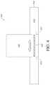
- FIG. 1is a schematic representation of a conventional substrate floatation system. More specifically, FIG. 1 shows a portion of a flotation system in which substrate 100 is supported by air bearings. The air bearings are shown schematically as arrows entering and leaving between baffles 110 .
- the substrate floatation system of FIG. 1is typically housed in a sealed chamber (not shown).
- the chamberincludes multiple vacuum outlet ports 120 and gas bearing inlet ports 130 , which are typically arranged on a flat surface 140 .
- Substrate 100is lifted and kept off a hard surface by the pressure of a gas such as nitrogen.
- the flow out of the bearing volumeis accomplished by means of multiple vacuum outlet ports 120 .
- the floating height 150is typically a function of the gas pressure and flow.
- any gascan be utilized for such a substrate floatation system; however, in practice it is preferable to utilize a floatation gas that is inert to the materials that come into contact with the gas.
- a floatation gasthat is inert to the materials that come into contact with the gas.
- noble gasese.g., nitrogen, argon, and helium
- the floatation gasis an expensive component of the substrate floatation system.
- the costis compounded when the printing system calls for substantially pure gas. Thus, it is desirable to minimize any gas loss to the environment.
- FIG. 2is a simplified representation of an exemplary load-locked printing housing according to one embodiment of the disclosure.
- Housing 200is divided into three chambers, including inlet chamber 210 , print-head chamber 220 and outlet chamber 230 .
- each chamberis separated from the rest of housing 200 through a gate or a partition.
- the gates or partitionssubstantially seal the chambers from the ambient environment and from the rest of housing 200 .
- chamber 230is not included in housing 200 , and chamber 210 is utilized as both an inlet and an outlet chamber.
- FIG. 3is a schematic representation of the load-locked printing housing of FIG. 2 receiving a substrate.
- substrate 350is received at inlet chamber 310 through inlet gates 312 .
- Inlet gates 312can comprise a variety of options, including single or multiple moving gates.
- the gatescan also be complemented with an air curtain (not shown) for minimizing influx of ambient gases into inlet chamber 310 .
- the gatescan be replaced with air curtains acting as a partition. Similar schemes can be deployed in all gates of the housing.
- the inlet chambercan be optionally purged from any ambient gases and refilled with the desired chamber gas, which is conventionally selected to be the same as the floatation gas, e.g. pure nitrogen or other noble gases.
- the desired chamber gaswhich is conventionally selected to be the same as the floatation gas, e.g. pure nitrogen or other noble gases.
- print-head inlet gate 322 as well as inlet gate 312remain closed.
- Print-head inlet gate 322can define a physical or a gas curtain.
- print-head inlet gate 322can define a physical gate similar to inlet gate 312 .
- FIG. 4schematically shows the substrate received at the print-head chamber of the housing.
- Air bearingscan be used to transport substrate 450 from inlet chamber 410 through print-head inlet gate 422 and into print-chamber 420 .
- Print-head chamber 420houses the thermal jet print-head, and optionally, the ink reservoir. The printing process occurs at print-head chamber 420 .
- print-head gates 422 and 424are closed during the printing process.
- Print-head chambercan be optionally purged with a chamber gas (e.g., high purity nitrogen) for further purification of the printing environment.
- substrate 450is printed while gates 422 and 424 remain open.
- substrate 450can be supported by air bearings.
- the substrate's location in relation to housing 400can be controlled using a combination of air pressure and vacuum, such as those shown in FIG. 1 .
- the substrateis transported through housing 400 using a conveyer belt.
- the substrateis transported to the outlet chamber as shown in FIG. 5 .
- print-head gates 522 and 524are closed to seal off outlet chamber 530 from the remainder of housing 500 .
- Outlet gate 532is opened to eject substrate 550 as indicated by the arrow.
- the process shown in FIGS. 3-5can be repeated to continuously print OLED materials on multiple substrates.
- gates 512 , 522 , 524 and 532can be replaced with air curtains to provide for continuous and uninterrupted printing process.
- the substrateis transported back to the inlet chamber 310 through gate 322 , where gate 322 can be subsequently sealed off and gate 312 opened to eject the substrate.
- inlet chamber 310functions also as the outlet chamber, functionally replacing outlet chamber 530 .
- the print-head chamberhouses the print-head.
- the print-headcomprises an ink chamber in fluid communication with nozzle.
- the ink chamberreceives ink, comprising particles of the material to be deposited on the substrate dissolved or suspended in a carrier liquid, in substantially liquid form from a reservoir.
- the ink head chamberthen meters a specified quantity of ink onto an upper face of a thermal jet discharge nozzle having a plurality of conduits such that upon delivery to the upper face, the ink flows into the conduits.
- the thermal jet discharge nozzleis activated such that the carrier liquid is removed leaving behind in the conduits the particles in substantially solid form.
- the thermal jet discharge nozzleis then further pulsatingly activated to deliver the quantity of material in substantially vapor form onto the substrate, where it condenses into substantially solid form.
- FIG. 6is a schematic representation of a thermal jet print-head for use with the load-locked housing of FIG. 2 .
- Print-head 600includes ink chamber 615 which is surrounded by top structure 610 and energizing element 620 .
- Ink chamber 615is in liquid communication with an ink reservoir (not shown).
- Energizing element 620can comprise a piezoelectric element or a heater. Energizing element 620 is energized intermittently to dispense a metered quantity of ink, optionally in the form of a liquid droplet, on the top surface of the thermal jet discharge nozzle 640 .
- Brackets 660can include and integrated heating element.
- the heating elementis capable of instantaneously heating thermal jet discharge nozzle 640 such that the ink carrier liquid evaporates from the conduits 650 .
- the heating elementis further capable of instantaneously heating the thermal jet discharge nozzle 650 such that substantially solid particles in the discharge nozzle are delivered from the conduits in substantially vapor form onto the substrate, where they condense into substantially solid form.
- Print-head 600operates entirely within the print-head chamber 220 and housing 200 of FIG. 2 .
- the load-locked housingcan be configured to receive a transport gas, such as a noble gas, for carrying the material from the thermal jet discharge nozzle 640 onto the substrate surface.
- the transport gasmay also transport the material from the thermal jet discharge nozzle 640 to the substrate by flowing through conduits 650 .
- multiple print-heads 600are arranged within a load-locked print system as an array. The array can be configured to deposit material on a substrate by activating the print-heads simultaneously or sequentially.
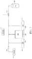
- FIG. 7is an exemplary load-locked system according to an embodiment of the invention.
- Load-locked system of FIG. 7includes a housing with inlet chamber 710 , print-head chamber 720 and outlet chamber 730 .
- Inlet chamber 710communicates through gates 712 and 722 .
- Print-head chamber 720receives substrate 750 from the inlet chamber and deposits organic LED material thereon as described in relation to FIG. 6 .
- Gate 724communicates substrate 750 to outlet chamber 730 after the printing process is completed. The substrate exists outlet chamber 730 through gate 732 .
- Vacuum and pressurecan be used to transport substrate 750 through the load-locked system of FIG. 7 .
- controller 770communicates with nitrogen source 762 and vacuum 760 through valves 772 and 774 , respectively.
- Controller 770comprises one or more processor circuits (not shown) in communication with one or more memory circuit (not shown).
- the controlleralso communicates with the load-locked housing and ultimately with the print nozzle. In this manner, controller 770 can coordinate opening and closing gates 712 , 722 , 724 and 732 .
- Controller 770can also control ink dispensing by activating the piezoelectric element and/or the heater (see FIG. 6 ).
- the substratecan be transported through the load-locked print system through air bearings or by a physical conveyer under the control of the controller.
- a memory circuit (not shown) of controller 770provides instructions to a processor circuit (not shown) to: (i) receive the substrate at the inlet partition; (ii) purge the housing with the first gas; (iii) direct the substrate to a discharge nozzle at the print-head chamber; (iv) energize the discharge nozzle to pulsatingly deliver a quantity of material from the thermal jet discharge nozzle onto the substrate; and (v) dispatch the substrate from the housing through the outlet partition.
- the first gas and the second gascan be different or identical gases.
- the first and/or the second gascan be selected from the group comprising nitrogen, argon, and helium.
- Controller 770may also identify the location of the substrate through the load-locked print system and dispense ink from the print-head only when the substrate is at a precise location relative to the print-head.
- Another aspect of the inventionrelates to registering the substrate relative to the print-head.
- Printing registrationis defined as the alignment and the size of one printing process with respect to the previous printing processes performed on the same substrate.
- the print-head and the substrateneed to be aligned substantially identically in each printing step.
- the substrateis provided with horizontal motion (i.e., motion in the x direction) and the print-head is provided with another horizontal motion (i.e., motion in the y direction).
- the x and y directionsmay be orthogonal to each other. With this arrangement, the movement of the print-head with respect to the substrate can be defined with a combination of these two horizontal directions.
- the areas to be printedare usually not perfectly aligned in the x and y directions of the system.
- the pattern or the previous printingis detected using a pattern recognition system.
- This patterncan be inherent in the previous printing or may have been added deliberately (i.e., fiducials) for the pattern recognition step.
- the misalignment of the substrate to the printing system's motion, direction or axiscan be determined. This manifests itself as a magnification misalignment, a translational misalignment and an angular misalignment.
- FIG. 8shows several types of substrate misalignment within the print system, including translational misalignment, rotational misalignment, magnification misalignment and combinational misalignment.
- the pattern recognition systemFor each print-head scan motion relative to the substrate, the pattern recognition system will look for and find/recognize the desired pattern.
- the pattern recognition systemcan optionally be integrated with the controller (see FIG. 7 ).
- the pattern recognition systemwill look for and find/recognize the desired pattern.
- the pattern recognition systemwill provide the degree of error/misalignment in the x and y directions to the system's controller, which will then reposition the print-head and substrate to eliminate the error/misalignment. This means that for several motions of the print-head with respect to the substrate, the motion control system will check for misalignment and make the necessary corrections.
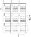
- FIG. 9shows a substrate pattern including fiducials and initial locus of area viewed by a camera or other imaging devices.
- fiducials or alignment targetsare identified as boxes 910 in each replicated “pixel.”
- the camera or the pattern recognition deviceinitially focuses on an area of the substrate identified by circle 930 .
- the motion control systemcan compensate for the misalignment by causing the x and the y directions to move in a rotated and translated set of axes x 1 and y 1 such that these axis are a linear combination of the previous motions.
- the printing control systemwill then cause the print-head to fire appropriately at the desired print axis as it scans the substrate.
- the print systemwill periodically use the pattern recognition system to update and adjust for any misalignment, causing the print-head to fire after alignment has been achieved.
- the required update and adjustment stepsmay have to be repeated more often during the printing operations.
- the pattern recognition systemmust scan the substrate initially to assess the amount and direction of misalignment, then printing control system will utilize the misalignment information to adjust the print-head firing accordingly.
- the principles of the disclosurehave been illustrated in relation to the exemplary embodiments shown herein, the principles of the disclosure are not limited thereto and include any modification, variation or permutation thereof.
- the exemplary embodimentsare discussed in relation to a thermal jet discharge nozzle, the disclosed principles can be implemented with different type of nozzles.
- the same or different gasescan be used for floating the substrate and for providing a non-oxidizing environment within the chamber. These gases need not be noble gases.
- the substratemay enter the system from any direction and the schematic of a tri-chamber system is entirely exemplary.
Landscapes
- Engineering & Computer Science (AREA)
- Manufacturing & Machinery (AREA)
- Physics & Mathematics (AREA)
- Chemical & Material Sciences (AREA)
- Condensed Matter Physics & Semiconductors (AREA)
- General Physics & Mathematics (AREA)
- Computer Hardware Design (AREA)
- Microelectronics & Electronic Packaging (AREA)
- Power Engineering (AREA)
- Plasma & Fusion (AREA)
- Chemical Kinetics & Catalysis (AREA)
- Materials Engineering (AREA)
- Mechanical Engineering (AREA)
- Metallurgy (AREA)
- Organic Chemistry (AREA)
- Electroluminescent Light Sources (AREA)
Abstract
Description
- This application is a continuation of U.S. patent application Ser. No. 15/409,844, filed on Jan. 19, 2017, which is a continuation of U.S. patent application Ser. No. 14/996,086, filed on Jan. 14, 2016, now U.S. Pat. No 10,519,535, issued on Dec. 31, 2019, which is a continuation of U.S. patent application Ser. No. 13/776,602, filed on Feb. 25, 2013, now U.S. Pat. No. 9,248,643, issued on Feb. 2, 2016, which is a divisional of U.S. patent application Ser. No. 13/551,209, filed on Jul. 17, 2012, now U.S. Pat. No. 8,720,366, issued on May 13, 2014, which is a continuation of U.S. patent application Ser. No. 12/652,040, filed on Jan. 5, 2010, now U.S. Pat. No. 8,383,202, issued on Feb. 26, 2013, which is a continuation-in-part of U.S. patent application Ser. No. 12/139,391, filed Jun. 13, 2008, now abandoned. U.S. patent application Ser. No. 12/652,040 also claims the benefit of U.S. Provisional Application No. 61/142,575, filed Jan. 5, 2009. All cross-referenced applications are herein incorporated in their entirety.
- The disclosure relates to a method and apparatus for efficient deposition of a patterned film on a substrate. More specifically, the disclosure relates to a method and apparatus for supporting and transporting a substrate on gas bearing during thermal jet printing of material on a substrate.
- The manufacture of organic light emitting devices (OLEDs) requires depositing one or more organic films on a substrate and coupling the top and bottom of the film stack to electrodes. The film thickness is a prime consideration. The total layer stack thickness is about 100 nm and each layer is optimally deposited uniformly with an accuracy of better than .+−.1 nm. Film purity is also important. Conventional apparatuses form the film stack using one of two methods: (1) thermal evaporation of organic material in a relative vacuum environment and subsequent condensation of the organic vapor on the substrate; or, (2) dissolution of organic material into a solvent, coating the substrate with the resulting solution, and subsequent removal of the solvent.
- Another consideration in depositing the organic thin films of an OLED is placing the films precisely at the desired location on the substrate. There are two conventional technologies for performing this task, depending on the method of film deposition. For thermal evaporation, shadow masking is used to form OLED films of a desired configuration. Shadow masking techniques require placing a well-defined mask over a region of the substrate followed by depositing the film over the entire substrate area. Once deposition is complete, the shadow mask is removed. The regions exposed through the mask define the pattern of material deposited on the substrate. This process is inefficient as the entire substrate must be coated, even though only the regions exposed through the shadow mask require a film. Furthermore, the shadow mask becomes increasingly coated with each use, and must eventually be discarded or cleaned. Finally, the use of shadow masks over large areas is made difficult by the need to use very thin masks (to achieve small feature sizes) that make said masks structurally unstable. However, the vapor deposition technique yields OLED films with high uniformity and purity and excellent thickness control.
- For solvent deposition, ink jet printing can be used to deposit patterns of OLED films. Ink jet printing requires dissolving organic material into a solvent that yields a printable ink. Furthermore, ink jet printing is conventionally limited to the use of single layer OLED film stacks, which typically have lower performance as compared to multilayer stacks. The single-layer limitation arises because printing typically causes destructive dissolution of any underlying organic layers. Finally, unless the substrate is first prepared to define the regions into which the ink is to be deposited, a step that increases the cost and complexity of the process, ink jet printing is limited to circular deposited areas with poor thickness uniformity as compared to vapor deposited films. The material quality is also lower due to structural changes in the material that occur during the drying process and due to material impurities present in the ink. However, the ink jet printing technique is capable of providing patterns of OLED films over very large areas with good material efficiency.
- No conventional technique combines the large area patterning capabilities of ink jet printing with the high uniformity, purity, and thickness control achieved with vapor deposition for organic thin films. Because ink jet processed single layer OLED devices continue to have inadequate quality for widespread commercialization, and thermal evaporation remains impractical for scaling to large areas, it is a major technological challenge for the OLED industry to develop a technique that can offer both high film quality and cost-effective large area scalability.
- Manufacturing OLED displays may also require the patterned deposition of thin films of metals, inorganic semiconductors, and/or inorganic insulators. Conventionally, vapor deposition and/or sputtering have been used to deposit these layers. Patterning is accomplished using prior substrate preparation (e.g., patterned coating with an insulator), shadow masking as described above, and when a fresh substrate or protective layers are employed, conventional photolithography. Each of these approaches is inefficient as compared to the direct deposition of the desired pattern, either because it wastes material or requires additional processing steps. Thus, for these materials as well there is a need for a method and apparatus for depositing high-quality, cost effective, large area scalable films.
- Certain applications of thermal jet printing require non-oxidizing environment to prevent oxidation of the deposited materials or associated inks. In a conventional method, a sealed nitrogen tent is used to prevent oxidation. Conventional systems use a floating system to support and move the substrate. A floatation system can be defined as a bearing system of alternative gas bearings and vacuum ports. The gas bearings provide the lubricity and non-contacting support for the substrate, while the vacuum supports the counter-force necessary to strictly control the height at which the relatively light-weight substrate floats. Since high-purity nitrogen gas can be a costly component of the printing system, it is important to minimize nitrogen loss to the ambient.
- Accordingly, there is a need for load-locked printing system which supports a substrate on gas bearings while minimizing system leakage and nitrogen loss.
- The disclosure relates to a method and apparatus for preventing oxidation or contamination during a thermal jet printing operation. The thermal jet printing operation may include OLED printing and the printing material may include suitable ink composition. In an exemplary embodiment, the printing process is conducted at a load-locked printer housing having one or more chambers. Each chamber is partitioned from the other chambers by physical gates or fluidic curtains. A controller coordinates transportation of a substrate through the system and purges the system by timely opening appropriate gates. The substrate may be transported using gas bearings which are formed using a plurality of vacuum and gas input portals. The controller may also provide a non-oxidizing environment within the chamber using a gas similar to, or different from, the gas used for the gas bearings. The controller may also control the printing operation by energizing the print-head at a time when the substrate is positioned substantially thereunder.
- In one embodiment, the disclosure relates to a method for printing a film of OLED material on a substrate by (i) receiving the substrate at an inlet chamber; (ii) flooding the inlet load-locked chamber with a noble gas and sealing the inlet chamber; (iii) directing at least a portion of the substrate to a print-head chamber and discharging a quantity of OLED material from a thermal jet discharge nozzle onto the portion of the substrate; (iv) directing the substrate to an outlet chamber; (v) partitioning the print-head chamber from the outlet chamber; and (vi) unloading the print-head from the outlet chamber. In one embodiment of the invention, the print-head chamber pulsatingly delivers a quantity of material from a thermal jet discharge nozzle to the substrate.
- In another embodiment, the disclosure relates to a method for depositing a material on a substrate. The method includes the steps of: (i) receiving the substrate at an inlet chamber; (ii) flooding the inlet chamber with a chamber gas and sealing the inlet chamber; (iii) directing at least a portion of the substrate to a print-head chamber and discharging a quantity of material from a thermal jet discharge nozzle onto the portion of the substrate; (iv) directing the substrate to an outlet chamber; (v) partitioning the print-head chamber from the outlet chamber; and (vi) unloading the print-head from the outlet chamber. The print-head chamber pulsatingly delivers a quantity of material from a thermal jet discharge nozzle to the substrate.
- In another embodiment, the disclosure relates to a load-locked printing apparatus, comprising an inlet chamber for receiving a substrate, the inlet chamber having a first partition and a second partition; a print-head chamber in communication with the inlet chamber, the print-head chamber having a discharge nozzle for pulsatingly metering a quantity of ink onto a substrate, the second partition separating the print-head chamber from the inlet chamber; an outlet chamber in communication with the print-head chamber through a third partition, the outlet chamber receiving the substrate from print head chamber and exiting the substrate from a fourth chamber. In a preferred embodiment, the inlet chamber, the print-head chamber and the outlet chamber provide an inert gas environment while the discharge nozzle pulsatingly meters the quantity of ink onto the substrate. Although the implementation of the invention are not limited thereto, the inert gas environment can be a noble gas (e.g. argon, helium, nitrogen or hydrogen).
- In still another embodiment, the disclosure relates to a load-locked thermal jet printing system. The system includes a housing with an inlet partition and an outlet partition. The housing defines a print-head chamber for depositing a quantity of ink onto a substrate. The housing also includes an inlet partition and an outlet partition for receiving and dispatching the substrate. A gas input provides a first gas to the housing. A controller communicates with the print-head chamber, the gas input and the inlet and outlet partitions. The controller comprises a processor circuit in communication with a memory circuit, the memory circuit instructing the processor circuit to (i) receive the substrate at the inlet partition; (ii) purge the housing with the first gas; (iii) direct the substrate to a discharge nozzle at the print-head chamber; (iv) energize the thermal jet discharge nozzle to pulsatingly deliver a quantity of film material from the discharge nozzle onto the substrate; and (v) dispatch the substrate from the housing through the outlet partition.
- These and other embodiments of the disclosure will be discussed with reference to the following exemplary and non-limiting illustrations, in which like elements are numbered similarly, and where:
FIG. 1 is a schematic representation of a conventional substrate floatation system;FIG. 2 is a schematic representation of an exemplary load-locked printing housing;FIG. 3 is a schematic representation of the load-locked printing housing ofFIG. 2 receiving a substrate;FIG. 4 schematically shows the substrate received at the print-head chamber of the housing;FIG. 5 schematically shows the completion of the printing process ofFIGS. 3 and 4 ;FIG. 6 is a schematic representation of a print-head for use with the load-locked housing ofFIG. 2 ; andFIG. 7 is an exemplary load-locked system according to an embodiment of the invention;FIG. 8 shows several types of substrate misalignment within the print system, andFIG. 9 shows a substrate pattern including fiducials and initial locus of area viewed by a camera or other imaging devices.FIG. 1 is a schematic representation of a conventional substrate floatation system. More specifically,FIG. 1 shows a portion of a flotation system in whichsubstrate 100 is supported by air bearings. The air bearings are shown schematically as arrows entering and leaving betweenbaffles 110. The substrate floatation system ofFIG. 1 is typically housed in a sealed chamber (not shown). The chamber includes multiplevacuum outlet ports 120 and gas bearinginlet ports 130, which are typically arranged on aflat surface 140.Substrate 100 is lifted and kept off a hard surface by the pressure of a gas such as nitrogen. The flow out of the bearing volume is accomplished by means of multiplevacuum outlet ports 120. The floatingheight 150 is typically a function of the gas pressure and flow. In principle, any gas can be utilized for such a substrate floatation system; however, in practice it is preferable to utilize a floatation gas that is inert to the materials that come into contact with the gas. As a result, it is conventional to use noble gases (e.g., nitrogen, argon, and helium) as they usually demonstrate sufficient inertness.- The floatation gas is an expensive component of the substrate floatation system. The cost is compounded when the printing system calls for substantially pure gas. Thus, it is desirable to minimize any gas loss to the environment.
FIG. 2 is a simplified representation of an exemplary load-locked printing housing according to one embodiment of the disclosure.Housing 200 is divided into three chambers, includinginlet chamber 210, print-head chamber 220 andoutlet chamber 230. As will be discussed, each chamber is separated from the rest ofhousing 200 through a gate or a partition. In one embodiment of the disclosure the gates or partitions substantially seal the chambers from the ambient environment and from the rest ofhousing 200. In another embodiment of the disclosure (not shown),chamber 230 is not included inhousing 200, andchamber 210 is utilized as both an inlet and an outlet chamber.FIG. 3 is a schematic representation of the load-locked printing housing ofFIG. 2 receiving a substrate. During operation,substrate 350 is received atinlet chamber 310 throughinlet gates 312.Inlet gates 312 can comprise a variety of options, including single or multiple moving gates. The gates can also be complemented with an air curtain (not shown) for minimizing influx of ambient gases intoinlet chamber 310. Alternatively, the gates can be replaced with air curtains acting as a partition. Similar schemes can be deployed in all gates of the housing. Oncesubstrate 350 is received atinlet chamber 310,inlet gates 312 close. The substrate can then be detained atinlet chamber 310. At this time, the inlet chamber can be optionally purged from any ambient gases and refilled with the desired chamber gas, which is conventionally selected to be the same as the floatation gas, e.g. pure nitrogen or other noble gases. During the purging process, print-head inlet gate 322 as well asinlet gate 312 remain closed. Print-head inlet gate 322 can define a physical or a gas curtain. Alternatively, print-head inlet gate 322 can define a physical gate similar toinlet gate 312.FIG. 4 schematically shows the substrate received at the print-head chamber of the housing. Air bearings can be used to transportsubstrate 450 frominlet chamber 410 through print-head inlet gate 422 and into print-chamber 420. Print-head chamber 420 houses the thermal jet print-head, and optionally, the ink reservoir. The printing process occurs at print-head chamber 420. In one implementation of the invention, oncesubstrate 450 is received at print-head chamber 420, print-head gates substrate 450 is printed whilegates substrate 450 can be supported by air bearings. The substrate's location in relation tohousing 400 can be controlled using a combination of air pressure and vacuum, such as those shown inFIG. 1 . In an alternative embodiment, the substrate is transported throughhousing 400 using a conveyer belt.- Once the printing process is complete, the substrate is transported to the outlet chamber as shown in
FIG. 5 . Here, print-head gates outlet chamber 530 from the remainder ofhousing 500.Outlet gate 532 is opened to ejectsubstrate 550 as indicated by the arrow. The process shown inFIGS. 3-5 can be repeated to continuously print OLED materials on multiple substrates. Alternatively,gates inlet chamber 310 throughgate 322, wheregate 322 can be subsequently sealed off andgate 312 opened to eject the substrate. In this embodiment,inlet chamber 310 functions also as the outlet chamber, functionally replacingoutlet chamber 530. - The print-head chamber houses the print-head. In a preferred embodiment, the print-head comprises an ink chamber in fluid communication with nozzle. The ink chamber receives ink, comprising particles of the material to be deposited on the substrate dissolved or suspended in a carrier liquid, in substantially liquid form from a reservoir. The ink head chamber then meters a specified quantity of ink onto an upper face of a thermal jet discharge nozzle having a plurality of conduits such that upon delivery to the upper face, the ink flows into the conduits. The thermal jet discharge nozzle is activated such that the carrier liquid is removed leaving behind in the conduits the particles in substantially solid form. The thermal jet discharge nozzle is then further pulsatingly activated to deliver the quantity of material in substantially vapor form onto the substrate, where it condenses into substantially solid form.
FIG. 6 is a schematic representation of a thermal jet print-head for use with the load-locked housing ofFIG. 2 . Print-head 600 includesink chamber 615 which is surrounded bytop structure 610 and energizingelement 620.Ink chamber 615 is in liquid communication with an ink reservoir (not shown). Energizingelement 620 can comprise a piezoelectric element or a heater. Energizingelement 620 is energized intermittently to dispense a metered quantity of ink, optionally in the form of a liquid droplet, on the top surface of the thermal jet discharge nozzle640.Bottom structure 630 supports nozzle640 throughbrackets 660.Brackets 660 can include and integrated heating element. The heating element is capable of instantaneously heating thermal jet discharge nozzle640 such that the ink carrier liquid evaporates from theconduits 650. The heating element is further capable of instantaneously heating the thermaljet discharge nozzle 650 such that substantially solid particles in the discharge nozzle are delivered from the conduits in substantially vapor form onto the substrate, where they condense into substantially solid form.- Print-
head 600 operates entirely within the print-head chamber 220 andhousing 200 ofFIG. 2 . Thus, for properly selected chamber and floatation gases (e.g. high purity nitrogen in most instances), the ink is not subject to oxidation during the deposition process. In addition, the load-locked housing can be configured to receive a transport gas, such as a noble gas, for carrying the material from the thermal jet discharge nozzle640 onto the substrate surface. The transport gas may also transport the material from the thermal jet discharge nozzle640 to the substrate by flowing throughconduits 650. In a preferred embodiment, multiple print-heads 600 are arranged within a load-locked print system as an array. The array can be configured to deposit material on a substrate by activating the print-heads simultaneously or sequentially. FIG. 7 is an exemplary load-locked system according to an embodiment of the invention. Load-locked system ofFIG. 7 includes a housing withinlet chamber 710, print-head chamber 720 andoutlet chamber 730.Inlet chamber 710 communicates throughgates head chamber 720 receivessubstrate 750 from the inlet chamber and deposits organic LED material thereon as described in relation toFIG. 6 .Gate 724 communicatessubstrate 750 tooutlet chamber 730 after the printing process is completed. The substrate existsoutlet chamber 730 throughgate 732.- Vacuum and pressure can be used to transport
substrate 750 through the load-locked system ofFIG. 7 . To control transporting the substrate,controller 770 communicates withnitrogen source 762 andvacuum 760 throughvalves Controller 770 comprises one or more processor circuits (not shown) in communication with one or more memory circuit (not shown). The controller also communicates with the load-locked housing and ultimately with the print nozzle. In this manner,controller 770 can coordinate opening and closinggates Controller 770 can also control ink dispensing by activating the piezoelectric element and/or the heater (seeFIG. 6 ). The substrate can be transported through the load-locked print system through air bearings or by a physical conveyer under the control of the controller. - In an exemplary operation, a memory circuit (not shown) of
controller 770 provides instructions to a processor circuit (not shown) to: (i) receive the substrate at the inlet partition; (ii) purge the housing with the first gas; (iii) direct the substrate to a discharge nozzle at the print-head chamber; (iv) energize the discharge nozzle to pulsatingly deliver a quantity of material from the thermal jet discharge nozzle onto the substrate; and (v) dispatch the substrate from the housing through the outlet partition. The first gas and the second gas can be different or identical gases. The first and/or the second gas can be selected from the group comprising nitrogen, argon, and helium. Controller 770 may also identify the location of the substrate through the load-locked print system and dispense ink from the print-head only when the substrate is at a precise location relative to the print-head.- Another aspect of the invention relates to registering the substrate relative to the print-head. Printing registration is defined as the alignment and the size of one printing process with respect to the previous printing processes performed on the same substrate. In order to achieve appropriate registration, the print-head and the substrate need to be aligned substantially identically in each printing step. In one implementation of the invention, the substrate is provided with horizontal motion (i.e., motion in the x direction) and the print-head is provided with another horizontal motion (i.e., motion in the y direction). The x and y directions may be orthogonal to each other. With this arrangement, the movement of the print-head with respect to the substrate can be defined with a combination of these two horizontal directions.
- When the substrate is loaded onto a load-locked system, the areas to be printed are usually not perfectly aligned in the x and y directions of the system. Thus, there is a need for detecting the misalignment, determining the required corrections to the motion of the print-head relative to the substrate and applying the corrections.
- According to one embodiment of the invention, the pattern or the previous printing is detected using a pattern recognition system. This pattern can be inherent in the previous printing or may have been added deliberately (i.e., fiducials) for the pattern recognition step. By means of its recognition of the pattern, the misalignment of the substrate to the printing system's motion, direction or axis can be determined. This manifests itself as a magnification misalignment, a translational misalignment and an angular misalignment.
FIG. 8 shows several types of substrate misalignment within the print system, including translational misalignment, rotational misalignment, magnification misalignment and combinational misalignment. For each print-head scan motion relative to the substrate, the pattern recognition system will look for and find/recognize the desired pattern. The pattern recognition system can optionally be integrated with the controller (seeFIG. 7 ). The pattern recognition system will look for and find/recognize the desired pattern. The pattern recognition system will provide the degree of error/misalignment in the x and y directions to the system's controller, which will then reposition the print-head and substrate to eliminate the error/misalignment. This means that for several motions of the print-head with respect to the substrate, the motion control system will check for misalignment and make the necessary corrections.- Alternatively, an initial scan of the entire substrate can be performed by the pattern recognition system utilizing the x and y motions available in the printing system.
FIG. 9 shows a substrate pattern including fiducials and initial locus of area viewed by a camera or other imaging devices. InFIG. 9 , fiducials or alignment targets are identified as boxes910 in each replicated “pixel.” Each pixel in this example, and in many OLED applications, comprises three sub-pixels each having a distinct color: red, green, and blue (RGB). The camera or the pattern recognition device initially focuses on an area of the substrate identified bycircle 930. Once the amount of misalignment is determined, the motion control system can compensate for the misalignment by causing the x and the y directions to move in a rotated and translated set of axes x1and y1such that these axis are a linear combination of the previous motions. - For either alignment technique, the printing control system will then cause the print-head to fire appropriately at the desired print axis as it scans the substrate. In the case of the embodiment described above, the print system will periodically use the pattern recognition system to update and adjust for any misalignment, causing the print-head to fire after alignment has been achieved. Depending on the degree of misalignment, the required update and adjustment steps may have to be repeated more often during the printing operations. Alternatively, the pattern recognition system must scan the substrate initially to assess the amount and direction of misalignment, then printing control system will utilize the misalignment information to adjust the print-head firing accordingly.
- While the principles of the disclosure have been illustrated in relation to the exemplary embodiments shown herein, the principles of the disclosure are not limited thereto and include any modification, variation or permutation thereof. For example, while the exemplary embodiments are discussed in relation to a thermal jet discharge nozzle, the disclosed principles can be implemented with different type of nozzles. Moreover, the same or different gases can be used for floating the substrate and for providing a non-oxidizing environment within the chamber. These gases need not be noble gases. Finally, the substrate may enter the system from any direction and the schematic of a tri-chamber system is entirely exemplary.
Claims (20)
Priority Applications (4)
| Application Number | Priority Date | Filing Date | Title |
|---|---|---|---|
| US16/949,412US11230757B2 (en) | 2008-06-13 | 2020-10-28 | Method and apparatus for load-locked printing |
| US17/450,713US11802331B2 (en) | 2008-06-13 | 2021-10-13 | Method and apparatus for load-locked printing |
| US17/804,419US11926902B2 (en) | 2008-06-13 | 2022-05-27 | Method and apparatus for load-locked printing |
| US18/429,872US12285945B2 (en) | 2008-06-13 | 2024-02-01 | Method and apparatus for load-locked printing |
Applications Claiming Priority (8)
| Application Number | Priority Date | Filing Date | Title |
|---|---|---|---|
| US12/139,391US20080311307A1 (en) | 2007-06-14 | 2008-06-13 | Method and apparatus for depositing films |
| US14257509P | 2009-01-05 | 2009-01-05 | |
| US12/652,040US8383202B2 (en) | 2008-06-13 | 2010-01-05 | Method and apparatus for load-locked printing |
| US13/551,209US8720366B2 (en) | 2008-06-13 | 2012-07-17 | Method and apparatus for load-locked printing |
| US13/776,602US9248643B2 (en) | 2008-06-13 | 2013-02-25 | Method and apparatus for load-locked printing |
| US14/996,086US10519535B2 (en) | 2008-06-13 | 2016-01-14 | Method and apparatus for load-locked printing |
| US15/409,844US10851450B2 (en) | 2008-06-13 | 2017-01-19 | Method and apparatus for load-locked printing |
| US16/949,412US11230757B2 (en) | 2008-06-13 | 2020-10-28 | Method and apparatus for load-locked printing |
Related Parent Applications (1)
| Application Number | Title | Priority Date | Filing Date |
|---|---|---|---|
| US15/409,844ContinuationUS10851450B2 (en) | 2008-06-13 | 2017-01-19 | Method and apparatus for load-locked printing |
Related Child Applications (1)
| Application Number | Title | Priority Date | Filing Date |
|---|---|---|---|
| US17/450,713ContinuationUS11802331B2 (en) | 2008-06-13 | 2021-10-13 | Method and apparatus for load-locked printing |
Publications (2)
| Publication Number | Publication Date |
|---|---|
| US20210040595A1true US20210040595A1 (en) | 2021-02-11 |
| US11230757B2 US11230757B2 (en) | 2022-01-25 |
Family
ID=42540080
Family Applications (14)
| Application Number | Title | Priority Date | Filing Date |
|---|---|---|---|
| US12/652,040Active2029-08-05US8383202B2 (en) | 2008-06-13 | 2010-01-05 | Method and apparatus for load-locked printing |
| US13/551,209ActiveUS8720366B2 (en) | 2008-06-13 | 2012-07-17 | Method and apparatus for load-locked printing |
| US13/773,649ActiveUS8802186B2 (en) | 2008-06-13 | 2013-02-22 | Method and apparatus for load-locked printing |
| US13/773,643ActiveUS8802195B2 (en) | 2008-06-13 | 2013-02-22 | Method and apparatus for load-locked printing |
| US13/774,577ActiveUS8807071B2 (en) | 2008-06-13 | 2013-02-22 | Method and apparatus for load-locked printing |
| US13/773,654ActiveUS8875648B2 (en) | 2008-06-13 | 2013-02-22 | Method and apparatus for load-locked printing |
| US13/774,683Active2028-12-21US9174433B2 (en) | 2008-06-13 | 2013-02-22 | Method and apparatus for load-locked printing |
| US13/776,602Active2029-04-08US9248643B2 (en) | 2008-06-13 | 2013-02-25 | Method and apparatus for load-locked printing |
| US14/996,086ActiveUS10519535B2 (en) | 2008-06-13 | 2016-01-14 | Method and apparatus for load-locked printing |
| US15/409,844ActiveUS10851450B2 (en) | 2008-06-13 | 2017-01-19 | Method and apparatus for load-locked printing |
| US16/949,412ActiveUS11230757B2 (en) | 2008-06-13 | 2020-10-28 | Method and apparatus for load-locked printing |
| US17/450,713Active2028-09-08US11802331B2 (en) | 2008-06-13 | 2021-10-13 | Method and apparatus for load-locked printing |
| US17/804,419ActiveUS11926902B2 (en) | 2008-06-13 | 2022-05-27 | Method and apparatus for load-locked printing |
| US18/429,872ActiveUS12285945B2 (en) | 2008-06-13 | 2024-02-01 | Method and apparatus for load-locked printing |
Family Applications Before (10)
| Application Number | Title | Priority Date | Filing Date |
|---|---|---|---|
| US12/652,040Active2029-08-05US8383202B2 (en) | 2008-06-13 | 2010-01-05 | Method and apparatus for load-locked printing |
| US13/551,209ActiveUS8720366B2 (en) | 2008-06-13 | 2012-07-17 | Method and apparatus for load-locked printing |
| US13/773,649ActiveUS8802186B2 (en) | 2008-06-13 | 2013-02-22 | Method and apparatus for load-locked printing |
| US13/773,643ActiveUS8802195B2 (en) | 2008-06-13 | 2013-02-22 | Method and apparatus for load-locked printing |
| US13/774,577ActiveUS8807071B2 (en) | 2008-06-13 | 2013-02-22 | Method and apparatus for load-locked printing |
| US13/773,654ActiveUS8875648B2 (en) | 2008-06-13 | 2013-02-22 | Method and apparatus for load-locked printing |
| US13/774,683Active2028-12-21US9174433B2 (en) | 2008-06-13 | 2013-02-22 | Method and apparatus for load-locked printing |
| US13/776,602Active2029-04-08US9248643B2 (en) | 2008-06-13 | 2013-02-25 | Method and apparatus for load-locked printing |
| US14/996,086ActiveUS10519535B2 (en) | 2008-06-13 | 2016-01-14 | Method and apparatus for load-locked printing |
| US15/409,844ActiveUS10851450B2 (en) | 2008-06-13 | 2017-01-19 | Method and apparatus for load-locked printing |
Family Applications After (3)
| Application Number | Title | Priority Date | Filing Date |
|---|---|---|---|
| US17/450,713Active2028-09-08US11802331B2 (en) | 2008-06-13 | 2021-10-13 | Method and apparatus for load-locked printing |
| US17/804,419ActiveUS11926902B2 (en) | 2008-06-13 | 2022-05-27 | Method and apparatus for load-locked printing |
| US18/429,872ActiveUS12285945B2 (en) | 2008-06-13 | 2024-02-01 | Method and apparatus for load-locked printing |
Country Status (1)
| Country | Link |
|---|---|
| US (14) | US8383202B2 (en) |
Families Citing this family (56)
| Publication number | Priority date | Publication date | Assignee | Title |
|---|---|---|---|---|
| US8986780B2 (en) | 2004-11-19 | 2015-03-24 | Massachusetts Institute Of Technology | Method and apparatus for depositing LED organic film |
| US8128753B2 (en) | 2004-11-19 | 2012-03-06 | Massachusetts Institute Of Technology | Method and apparatus for depositing LED organic film |
| EP2155494A4 (en)* | 2007-06-14 | 2010-08-11 | Massachusetts Inst Technology | METHOD AND APPARATUS FOR REGULATING A FILM DEPOSITION |
| US8556389B2 (en) | 2011-02-04 | 2013-10-15 | Kateeva, Inc. | Low-profile MEMS thermal printhead die having backside electrical connections |
| US10434804B2 (en) | 2008-06-13 | 2019-10-08 | Kateeva, Inc. | Low particle gas enclosure systems and methods |
| US10442226B2 (en) | 2008-06-13 | 2019-10-15 | Kateeva, Inc. | Gas enclosure assembly and system |
| US12018857B2 (en) | 2008-06-13 | 2024-06-25 | Kateeva, Inc. | Gas enclosure assembly and system |
| US12064979B2 (en) | 2008-06-13 | 2024-08-20 | Kateeva, Inc. | Low-particle gas enclosure systems and methods |
| US8899171B2 (en) | 2008-06-13 | 2014-12-02 | Kateeva, Inc. | Gas enclosure assembly and system |
| US9604245B2 (en) | 2008-06-13 | 2017-03-28 | Kateeva, Inc. | Gas enclosure systems and methods utilizing an auxiliary enclosure |
| US8632145B2 (en) | 2008-06-13 | 2014-01-21 | Kateeva, Inc. | Method and apparatus for printing using a facetted drum |
| US9048344B2 (en) | 2008-06-13 | 2015-06-02 | Kateeva, Inc. | Gas enclosure assembly and system |
| US11975546B2 (en) | 2008-06-13 | 2024-05-07 | Kateeva, Inc. | Gas enclosure assembly and system |
| US8383202B2 (en)* | 2008-06-13 | 2013-02-26 | Kateeva, Inc. | Method and apparatus for load-locked printing |
| US20100188457A1 (en)* | 2009-01-05 | 2010-07-29 | Madigan Connor F | Method and apparatus for controlling the temperature of an electrically-heated discharge nozzle |
| EP2425470A2 (en)* | 2009-05-01 | 2012-03-07 | Kateeva, Inc. | Method and apparatus for organic vapor printing |
| FI124113B (en)* | 2010-08-30 | 2014-03-31 | Beneq Oy | Apparatus and method for working the surface of a substrate |
| US9120344B2 (en) | 2011-08-09 | 2015-09-01 | Kateeva, Inc. | Apparatus and method for control of print gap |
| CN106299116B (en) | 2011-08-09 | 2019-07-12 | 科迪华公司 | Printing device and method downwards |
| TWI651500B (en)* | 2012-11-30 | 2019-02-21 | 美商凱特伊夫公司 | Method for maintenance of an industrial printing system |
| KR102326995B1 (en)* | 2012-11-30 | 2021-11-16 | 카티바, 인크. | A method for maintenance of an industrial printing system |
| CN104129163B (en)* | 2012-12-19 | 2016-03-23 | 科迪华公司 | Gas enclosure components and systems |
| US9832428B2 (en) | 2012-12-27 | 2017-11-28 | Kateeva, Inc. | Fast measurement of droplet parameters in industrial printing system |
| US9352561B2 (en) | 2012-12-27 | 2016-05-31 | Kateeva, Inc. | Techniques for print ink droplet measurement and control to deposit fluids within precise tolerances |
| US12330178B2 (en) | 2012-12-27 | 2025-06-17 | Kateeva, Inc. | Techniques for arrayed printing of a permanent layer with improved speed and accuracy |
| US11673155B2 (en) | 2012-12-27 | 2023-06-13 | Kateeva, Inc. | Techniques for arrayed printing of a permanent layer with improved speed and accuracy |
| CN105073434B (en) | 2012-12-27 | 2017-12-26 | 科迪华公司 | Method and system for printing ink volume control to deposit fluid within precise tolerances |
| US9700908B2 (en) | 2012-12-27 | 2017-07-11 | Kateeva, Inc. | Techniques for arrayed printing of a permanent layer with improved speed and accuracy |
| US11141752B2 (en) | 2012-12-27 | 2021-10-12 | Kateeva, Inc. | Techniques for arrayed printing of a permanent layer with improved speed and accuracy |
| CN109130549B (en)* | 2013-03-13 | 2021-02-26 | 科迪华公司 | Gas enclosure system and method of using auxiliary enclosure |
| KR20180128524A (en) | 2013-04-26 | 2018-12-03 | 카티바, 인크. | Techniques for print ink droplet measurement and control to deposit fluids within precise tolerances |
| CN105431294B (en)* | 2013-06-10 | 2018-04-24 | 科迪华公司 | Low particulate gas containment systems and methods |
| CN107264083B (en)* | 2013-10-02 | 2019-11-19 | 科迪华公司 | Apparatus and method for controlling printing gap |
| CN107825886B (en) | 2013-12-12 | 2020-04-14 | 科迪华公司 | Method of manufacturing electronic device |
| US10468279B2 (en) | 2013-12-26 | 2019-11-05 | Kateeva, Inc. | Apparatus and techniques for thermal treatment of electronic devices |
| US9343678B2 (en) | 2014-01-21 | 2016-05-17 | Kateeva, Inc. | Apparatus and techniques for electronic device encapsulation |
| KR102307190B1 (en)* | 2014-01-21 | 2021-09-30 | 카티바, 인크. | Apparatus and techniques for electronic device encapsulation |
| EP3882961B1 (en)* | 2014-04-30 | 2023-07-26 | Kateeva, Inc. | Gas cushion apparatus and techniques for substrate coating |
| US12251946B2 (en) | 2014-06-17 | 2025-03-18 | Kateeva, Inc. | Printing system assemblies and methods |
| KR20240036141A (en) | 2014-06-17 | 2024-03-19 | 카티바, 인크. | Printing system assemblies and methods |
| US11267012B2 (en) | 2014-06-25 | 2022-03-08 | Universal Display Corporation | Spatial control of vapor condensation using convection |
| US11220737B2 (en)* | 2014-06-25 | 2022-01-11 | Universal Display Corporation | Systems and methods of modulating flow during vapor jet deposition of organic materials |
| EP2960059B1 (en) | 2014-06-25 | 2018-10-24 | Universal Display Corporation | Systems and methods of modulating flow during vapor jet deposition of organic materials |
| JP6592019B2 (en) | 2014-07-18 | 2019-10-16 | カティーバ, インコーポレイテッド | Gas enclosure system and method utilizing multi-zone circulation and filtration |
| CN104260554B (en)* | 2014-09-24 | 2016-03-30 | 京东方科技集团股份有限公司 | Inkjet printing method and device, and manufacturing method of display substrate |
| CN104353584A (en)* | 2014-11-19 | 2015-02-18 | 京东方科技集团股份有限公司 | Coating device and coating method |
| WO2016086192A1 (en)* | 2014-11-26 | 2016-06-02 | Kateeva, Inc. | Environmentally controlled coating systems |
| JP6018659B2 (en)* | 2015-02-27 | 2016-11-02 | 株式会社日本製鋼所 | Atmosphere forming apparatus and levitation conveyance method |
| KR102342812B1 (en)* | 2015-03-16 | 2021-12-23 | 삼성디스플레이 주식회사 | Manufaturing device of organic light emitting diode display and method for manufacturing organic light emitting diode display using the same |
| CN107848309B (en)* | 2015-07-31 | 2020-05-19 | 科迪华公司 | Ink delivery system and method |
| US10566534B2 (en) | 2015-10-12 | 2020-02-18 | Universal Display Corporation | Apparatus and method to deliver organic material via organic vapor-jet printing (OVJP) |
| US9961782B2 (en) | 2016-07-08 | 2018-05-01 | Kateeva, Inc. | Transport path correction techniques and related systems, methods and devices |
| US11552247B2 (en)* | 2019-03-20 | 2023-01-10 | The Regents Of The University Of Michigan | Organic vapor jet nozzle with shutter |
| CN110943012B (en)* | 2019-11-22 | 2021-05-07 | 深圳市华星光电半导体显示技术有限公司 | Printing device for preparing OLED film and printing method thereof |
| US11292245B2 (en) | 2020-01-03 | 2022-04-05 | Trustees Of Boston University | Microelectromechanical shutters for organic vapor jet printing |
| CN115157876B (en)* | 2022-06-24 | 2023-09-29 | 昆山国显光电有限公司 | Printing and drying device and preparation method of display panel |
Family Cites Families (333)
| Publication number | Priority date | Publication date | Assignee | Title |
|---|---|---|---|---|
| US3216858A (en) | 1963-04-26 | 1965-11-09 | Cons Edison Co New York Inc | Method of purging gas-conduit tubing in gas-filled electric cables |
| US3251139A (en) | 1965-03-10 | 1966-05-17 | Us Dynamics Mfg Corp | Dynamic insulating systems |
| US3498343A (en) | 1966-12-13 | 1970-03-03 | Lawrence R Sperberg | Apparatus for inflating pneumatic tires with an inert gas |
| US3632374A (en)* | 1968-06-03 | 1972-01-04 | Eastman Kodak Co | Method of making photographic elements |
| US3670466A (en) | 1970-08-03 | 1972-06-20 | Metal Products Corp | Insulated panel |
| JPS549294B2 (en) | 1972-02-16 | 1979-04-23 | ||
| US3885362A (en) | 1973-04-19 | 1975-05-27 | Gordon J Pollock | Modular noise abatement enclosure and joint seal |
| JPS549294A (en) | 1977-06-22 | 1979-01-24 | Asahi Chem Ind Co Ltd | 7alpha-methoxycephalosporins and process for their preparation |
| US4226897A (en) | 1977-12-05 | 1980-10-07 | Plasma Physics Corporation | Method of forming semiconducting materials and barriers |
| IT1116334B (en) | 1977-12-28 | 1986-02-10 | Olivetti & Co Spa | IMPACT-FREE WRITING DEVICE WITH SELECTIVE EMISSION OF SOLID INK PARTICLES |
| US4409889A (en) | 1981-11-02 | 1983-10-18 | Burleson Maurice L | Modular clean room |
| US4581478A (en) | 1982-04-07 | 1986-04-08 | Pugh Paul F | Gas pressurized cable and conduit system |
| NL8203318A (en) | 1982-08-24 | 1984-03-16 | Integrated Automation | DEVICE FOR PROCESSING SUBSTRATES. |
| US5202659A (en)* | 1984-04-16 | 1993-04-13 | Dataproducts, Corporation | Method and apparatus for selective multi-resonant operation of an ink jet controlling dot size |
| JPS6172947A (en) | 1984-09-18 | 1986-04-15 | Takasago Thermal Eng Co Ltd | Clean room formation method and air conditioning equipment unit used in this method |
| US4721121A (en) | 1984-11-16 | 1988-01-26 | Adams Charles R | Combination pressing comb dryer and blow dryer |
| JPS6298783A (en) | 1985-10-25 | 1987-05-08 | Toshiba Corp | light emitting diode |
| JPH037588Y2 (en) | 1985-12-13 | 1991-02-25 | ||
| US4676144A (en) | 1985-12-30 | 1987-06-30 | Smithkline Beckman Corporation | Clean room system |
| US4751531A (en)* | 1986-03-27 | 1988-06-14 | Fuji Xerox Co., Ltd. | Thermal-electrostatic ink jet recording apparatus |
| EP0257633B2 (en)* | 1986-08-27 | 1995-01-25 | Hitachi, Ltd. | Heat transfer process and heat transfer ink sheet for use in the process |
| US5041161A (en)* | 1988-02-24 | 1991-08-20 | Dataproducts Corporation | Semi-solid ink jet and method of using same |
| US5065169A (en) | 1988-03-21 | 1991-11-12 | Hewlett-Packard Company | Device to assure paper flatness and pen-to-paper spacing during printing |
| JP2575205B2 (en)* | 1989-01-13 | 1997-01-22 | キヤノン株式会社 | Ink tank |
| GB8909011D0 (en)* | 1989-04-20 | 1989-06-07 | Friend Richard H | Electroluminescent devices |
| JP2836749B2 (en) | 1989-05-09 | 1998-12-14 | 株式会社リコー | Liquid jet recording head |
| US5029518A (en) | 1989-10-16 | 1991-07-09 | Clean Air Technology, Inc. | Modular clean room structure |
| KR960007979B1 (en) | 1991-04-17 | 1996-06-17 | 마쯔시다덴기산교 가부시기가이샤 | Clinic Space System |
| JP2943427B2 (en) | 1991-08-16 | 1999-08-30 | 富士電機株式会社 | Motor reversible operation device |
| JPH05218176A (en) | 1992-02-07 | 1993-08-27 | Tokyo Electron Tohoku Kk | Heat treatment and transfer of article to be treated |
| JP3206094B2 (en) | 1992-03-16 | 2001-09-04 | 株式会社リコー | Hot melt ink composition and recording method using the same |
| JP3136823B2 (en) | 1992-08-24 | 2001-02-19 | ソニー株式会社 | Ink jet print head and ink jet printer |
| US5314377A (en) | 1992-10-05 | 1994-05-24 | Airo Clean Inc. | Clean air isolation enclosure |
| US6189989B1 (en)* | 1993-04-12 | 2001-02-20 | Canon Kabushiki Kaisha | Embroidering using ink jet printing apparatus |
| US5896154A (en) | 1993-04-16 | 1999-04-20 | Hitachi Koki Co., Ltd. | Ink jet printer |
| DK85093D0 (en) | 1993-07-16 | 1993-07-16 | Landsforeningen Til Kraeftens | METHOD AND APPARATUS FOR PERFORMING OPERATIONS |
| US5344365A (en) | 1993-09-14 | 1994-09-06 | Sematech, Inc. | Integrated building and conveying structure for manufacturing under ultraclean conditions |
| US5405710A (en)* | 1993-11-22 | 1995-04-11 | At&T Corp. | Article comprising microcavity light sources |
| US5623292A (en)* | 1993-12-17 | 1997-04-22 | Videojet Systems International, Inc. | Temperature controller for ink jet printing |
| US5801721A (en)* | 1994-09-09 | 1998-09-01 | Signtech U.S.A. Ltd. | Apparatus for producing an image on a first side of a substrate and a mirror image on a second side of the substrate |
| US5574485A (en)* | 1994-10-13 | 1996-11-12 | Xerox Corporation | Ultrasonic liquid wiper for ink jet printhead maintenance |
| JPH08118641A (en)* | 1994-10-20 | 1996-05-14 | Canon Inc | Inkjet head, inkjet head cartridge, inkjet device, and ink container for inkjet head cartridge in which ink is re-injected |
| US6548956B2 (en)* | 1994-12-13 | 2003-04-15 | The Trustees Of Princeton University | Transparent contacts for organic devices |
| US5703436A (en) | 1994-12-13 | 1997-12-30 | The Trustees Of Princeton University | Transparent contacts for organic devices |
| US5707745A (en)* | 1994-12-13 | 1998-01-13 | The Trustees Of Princeton University | Multicolor organic light emitting devices |
| JP3575103B2 (en)* | 1995-02-17 | 2004-10-13 | ソニー株式会社 | Recording method |
| US5651625A (en) | 1995-04-10 | 1997-07-29 | Security Operating Systems, Inc. | Printer enclosure and controller unit |
| US6086196A (en)* | 1995-04-14 | 2000-07-11 | Sony Corporation | Printing device |
| KR100244041B1 (en) | 1995-08-05 | 2000-02-01 | 엔도 마코토 | Substrate processing apparatus |
| JPH0950374A (en) | 1995-08-09 | 1997-02-18 | Toshiba Corp | Variable length delayed slot pipeline controller |
| JPH09248918A (en) | 1996-03-15 | 1997-09-22 | Sharp Corp | Image recording device |
| US6586763B2 (en)* | 1996-06-25 | 2003-07-01 | Northwestern University | Organic light-emitting diodes and methods for assembly and emission control |
| US5844363A (en) | 1997-01-23 | 1998-12-01 | The Trustees Of Princeton Univ. | Vacuum deposited, non-polymeric flexible organic light emitting devices |
| US6091195A (en)* | 1997-02-03 | 2000-07-18 | The Trustees Of Princeton University | Displays having mesa pixel configuration |
| US5834893A (en) | 1996-12-23 | 1998-11-10 | The Trustees Of Princeton University | High efficiency organic light emitting devices with light directing structures |
| US6013982A (en)* | 1996-12-23 | 2000-01-11 | The Trustees Of Princeton University | Multicolor display devices |
| US6049167A (en) | 1997-02-17 | 2000-04-11 | Tdk Corporation | Organic electroluminescent display device, and method and system for making the same |
| JP3460500B2 (en) | 1997-03-14 | 2003-10-27 | 株式会社荏原製作所 | Gas cleaning apparatus, method for cleaning closed space using the same, and closed space |
| US5956051A (en)* | 1997-05-29 | 1999-09-21 | Pitney Bowes Inc. | Disabling a mailing machine when a print head is not installed |
| US5951770A (en) | 1997-06-04 | 1999-09-14 | Applied Materials, Inc. | Carousel wafer transfer system |
| US5865860A (en)* | 1997-06-20 | 1999-02-02 | Imra America, Inc. | Process for filling electrochemical cells with electrolyte |
| US6095630A (en)* | 1997-07-02 | 2000-08-01 | Sony Corporation | Ink-jet printer and drive method of recording head for ink-jet printer |
| US5898179A (en) | 1997-09-10 | 1999-04-27 | Orion Equipment, Inc. | Method and apparatus for controlling a workpiece in a vacuum chamber |
| US20030166104A1 (en) | 1997-09-18 | 2003-09-04 | Genentech, Inc. | Secreted and transmembrane polypeptides and nucleic acids encoding the same |
| US6303238B1 (en)* | 1997-12-01 | 2001-10-16 | The Trustees Of Princeton University | OLEDs doped with phosphorescent compounds |
| KR100232852B1 (en) | 1997-10-15 | 1999-12-01 | 윤종용 | Inkjet Printer Head and Manufacturing Method Thereof |
| US6086679A (en)* | 1997-10-24 | 2000-07-11 | Quester Technology, Inc. | Deposition systems and processes for transport polymerization and chemical vapor deposition |
| US6453810B1 (en)* | 1997-11-07 | 2002-09-24 | Speedline Technologies, Inc. | Method and apparatus for dispensing material in a printer |
| US5947022A (en)* | 1997-11-07 | 1999-09-07 | Speedline Technologies, Inc. | Apparatus for dispensing material in a printer |
| US6065825A (en)* | 1997-11-13 | 2000-05-23 | Eastman Kodak Company | Printer having mechanically-assisted ink droplet separation and method of using same |
| US6337102B1 (en)* | 1997-11-17 | 2002-01-08 | The Trustees Of Princeton University | Low pressure vapor phase deposition of organic thin films |
| US6087196A (en)* | 1998-01-30 | 2000-07-11 | The Trustees Of Princeton University | Fabrication of organic semiconductor devices using ink jet printing |
| JPH11312640A (en) | 1998-02-25 | 1999-11-09 | Canon Inc | Processing apparatus and device manufacturing method using the processing apparatus |
| US6326224B1 (en) | 1998-04-27 | 2001-12-04 | Motorola, Inc. | Method of purifying a primary color generated by an OED |
| US6312123B1 (en) | 1998-05-01 | 2001-11-06 | L&P Property Management Company | Method and apparatus for UV ink jet printing on fabric and combination printing and quilting thereby |
| US6089282A (en) | 1998-05-08 | 2000-07-18 | Aeronex, Inc. | Method for recovery and reuse of gas |
| TW399344B (en) | 1998-09-09 | 2000-07-21 | Jan Shr Shiung | High intensity light emitting diode (LED) and the manufacturing method thereof |
| EP1039547B1 (en)* | 1998-09-10 | 2016-03-23 | Mitsubishi Denki Kabushiki Kaisha | Semiconductor device |
| US6097147A (en)* | 1998-09-14 | 2000-08-01 | The Trustees Of Princeton University | Structure for high efficiency electroluminescent device |
| US6086195A (en)* | 1998-09-24 | 2000-07-11 | Hewlett-Packard Company | Filter for an inkjet printhead |
| GB9822963D0 (en)* | 1998-10-20 | 1998-12-16 | Agner Erik | Improvements in or relating to chromatography |
| US6023899A (en) | 1998-11-03 | 2000-02-15 | Climatecraft Technologies, Inc. | Wall panel assembly with airtight joint |
| TW442891B (en) | 1998-11-17 | 2001-06-23 | Tokyo Electron Ltd | Vacuum processing system |
| JP2000223548A (en) | 1999-01-28 | 2000-08-11 | Toshiba Corp | Display device manufacturing equipment |
| US6250747B1 (en)* | 1999-01-28 | 2001-06-26 | Hewlett-Packard Company | Print cartridge with improved back-pressure regulation |
| WO2000055891A1 (en) | 1999-03-12 | 2000-09-21 | Nikon Corporation | Exposure device, exposure method, and device manufacturing method |
| DE60011764T2 (en) | 1999-04-07 | 2005-07-07 | Mv Research Ltd. | WERKSTOFFPRÜFUNG |
| US6203151B1 (en)* | 1999-06-08 | 2001-03-20 | Hewlett-Packard Company | Apparatus and method using ultrasonic energy to fix ink to print media |
| TW504941B (en)* | 1999-07-23 | 2002-10-01 | Semiconductor Energy Lab | Method of fabricating an EL display device, and apparatus for forming a thin film |
| US6444400B1 (en)* | 1999-08-23 | 2002-09-03 | Agfa-Gevaert | Method of making an electroconductive pattern on a support |
| JP2001107272A (en)* | 1999-10-08 | 2001-04-17 | Hitachi Ltd | Sample processing method and processing apparatus, and magnetic head manufacturing method |
| US6294398B1 (en)* | 1999-11-23 | 2001-09-25 | The Trustees Of Princeton University | Method for patterning devices |
| KR100319772B1 (en) | 1999-12-02 | 2002-01-09 | 오길록 | Organic Micro-Cavity Laser |
| US6312083B1 (en) | 1999-12-20 | 2001-11-06 | Xerox Corporation | Printhead assembly with ink monitoring system |
| US6276782B1 (en) | 2000-01-11 | 2001-08-21 | Eastman Kodak Company | Assisted drop-on-demand inkjet printer |
| US6375304B1 (en) | 2000-02-17 | 2002-04-23 | Lexmark International, Inc. | Maintenance mist control |
| CN1416365A (en) | 2000-02-22 | 2003-05-07 | 基因谱公司 | Microarray fabrication tech and appts. |
| JP2001298068A (en) | 2000-04-18 | 2001-10-26 | Natl Inst Of Advanced Industrial Science & Technology Meti | Local cleaning method and local cleaning processing equipment |
| US6604810B1 (en) | 2000-05-23 | 2003-08-12 | Silverbrook Research Pty Ltd | Printhead capping arrangement |
| US6663219B2 (en) | 2000-06-01 | 2003-12-16 | Canon Kabushiki Kaisha | Inkjet recording apparatus |
| KR100408269B1 (en)* | 2000-07-20 | 2003-12-01 | 삼성전자주식회사 | Ink jet print head |
| US6755519B2 (en) | 2000-08-30 | 2004-06-29 | Creo Inc. | Method for imaging with UV curable inks |
| JP2002069650A (en) | 2000-08-31 | 2002-03-08 | Applied Materials Inc | Vapor phase deposition method and apparatus, and semiconductor device manufacturing method and apparatus |
| JP2002093878A (en) | 2000-09-12 | 2002-03-29 | Hitachi Kokusai Electric Inc | Semiconductor manufacturing equipment |
| US6781684B1 (en) | 2000-11-07 | 2004-08-24 | Donald L. Ekhoff | Workpiece levitation using alternating positive and negative pressure flows |
| US6601936B2 (en)* | 2000-11-14 | 2003-08-05 | Cypress Semiconductor Corp. | Real time adaptive inkjet temperature regulation controller |
| JP2007147648A (en) | 2000-12-01 | 2007-06-14 | Ebara Corp | Defect inspection method and substrate inspection device |
| JP3939101B2 (en) | 2000-12-04 | 2007-07-04 | 株式会社荏原製作所 | Substrate transport method and substrate transport container |
| DE10061628B4 (en) | 2000-12-11 | 2006-06-08 | Leica Microsystems Wetzlar Gmbh | Apparatus and method for gripping and transporting wafers |
| US6646284B2 (en) | 2000-12-12 | 2003-11-11 | Semiconductor Energy Laboratory Co., Ltd. | Light emitting device and method of manufacturing the same |
| US6513903B2 (en)* | 2000-12-29 | 2003-02-04 | Eastman Kodak Company | Ink jet print head with capillary flow cleaning |
| DE60227731D1 (en)* | 2001-02-09 | 2008-09-04 | Seiko Epson Corp | Ink jet recording device, control and Tintennachfüllsverfahren performed in the device, ink supply system in the device, and management methods of the ink supplied by the system |
| US6629756B2 (en)* | 2001-02-20 | 2003-10-07 | Lexmark International, Inc. | Ink jet printheads and methods therefor |
| US6688798B2 (en) | 2001-02-27 | 2004-02-10 | Incumed, Inc. | Adjustable locking mount and methods of use |
| US6472962B1 (en) | 2001-05-17 | 2002-10-29 | Institute Of Microelectronics | Inductor-capacitor resonant RF switch |
| JP2002359180A (en) | 2001-06-01 | 2002-12-13 | Toshiba Corp | Gas circulation system |
| JP2003017543A (en)* | 2001-06-28 | 2003-01-17 | Hitachi Kokusai Electric Inc | Substrate processing apparatus, substrate processing method, semiconductor device manufacturing method, and transfer apparatus |
| FR2827682B1 (en) | 2001-07-20 | 2004-04-02 | Gemplus Card Int | PRESSURE REGULATION BY TRANSFER OF A CALIBRATED GAS VOLUME |
| JP4971560B2 (en) | 2001-08-06 | 2012-07-11 | キヤノン株式会社 | Inkjet recording apparatus, head unit, and color filter manufacturing apparatus |
| US6824262B2 (en) | 2001-08-10 | 2004-11-30 | Seiko Epson Corporation | Ink set and ink jet recording method |
| US6878636B2 (en)* | 2001-08-27 | 2005-04-12 | Applied Materials, Inc. | Method for enhancing substrate processing |
| US7431968B1 (en)* | 2001-09-04 | 2008-10-07 | The Trustees Of Princeton University | Process and apparatus for organic vapor jet deposition |
| US7404862B2 (en) | 2001-09-04 | 2008-07-29 | The Trustees Of Princeton University | Device and method for organic vapor jet deposition |
| WO2003025245A1 (en)* | 2001-09-14 | 2003-03-27 | University Of Delaware | Multiple-nozzle thermal evaporation source |
| US6644149B2 (en) | 2001-09-17 | 2003-11-11 | Newfrey Llc | Extraction tool for tanged helically coiled inserts with improved removability |
| TW529317B (en) | 2001-10-16 | 2003-04-21 | Chi Mei Electronic Corp | Method of evaporating film used in an organic electro-luminescent display |
| US6733734B2 (en) | 2001-10-31 | 2004-05-11 | Matheson Tri-Gas | Materials and methods for the purification of hydride gases |
| US6460972B1 (en)* | 2001-11-06 | 2002-10-08 | Eastman Kodak Company | Thermal actuator drop-on-demand apparatus and method for high frequency |
| JP3868280B2 (en) | 2001-12-04 | 2007-01-17 | 株式会社美和製作所 | Organic electroluminescence device manufacturing equipment |
| US6939212B1 (en) | 2001-12-21 | 2005-09-06 | Lam Research Corporation | Porous material air bearing platen for chemical mechanical planarization |
| TWI222423B (en)* | 2001-12-27 | 2004-10-21 | Orbotech Ltd | System and methods for conveying and transporting levitated articles |
| JP4066661B2 (en) | 2002-01-23 | 2008-03-26 | セイコーエプソン株式会社 | Organic EL device manufacturing apparatus and droplet discharge apparatus |
| US6582875B1 (en) | 2002-01-23 | 2003-06-24 | Eastman Kodak Company | Using a multichannel linear laser light beam in making OLED devices by thermal transfer |
| US20030168174A1 (en) | 2002-03-08 | 2003-09-11 | Foree Michael Todd | Gas cushion susceptor system |
| US7081912B2 (en) | 2002-03-11 | 2006-07-25 | Seiko Epson Corporation | Optical writing head such as organic EL array exposure head, method of manufacturing the same, and image forming apparatus using the same |
| JP3925257B2 (en) | 2002-03-15 | 2007-06-06 | セイコーエプソン株式会社 | Connection line penetrating structure in airtight chamber, discharge device including the same, liquid crystal display device manufacturing method, organic EL device manufacturing method, electron emission device manufacturing method, PDP device manufacturing method, electrophoretic display device manufacturing Method, color filter manufacturing method, organic EL manufacturing method, spacer forming method, metal wiring forming method, lens forming method, resist forming method, and light diffuser forming method |
| JP3979135B2 (en) | 2002-03-20 | 2007-09-19 | セイコーエプソン株式会社 | Chamber device, electro-optical device and organic EL device including the same |
| US7133905B2 (en)* | 2002-04-09 | 2006-11-07 | Akamai Technologies, Inc. | Method and system for tiered distribution in a content delivery network |
| JP4543617B2 (en) | 2002-04-22 | 2010-09-15 | セイコーエプソン株式会社 | Active matrix substrate manufacturing method, electro-optical device manufacturing method, electronic device manufacturing method, active matrix substrate manufacturing device, electro-optical device manufacturing device, and electric device manufacturing device |
| DE10224128A1 (en) | 2002-05-29 | 2003-12-18 | Schmid Rhyner Ag Adliswil | Method of applying coatings to surfaces |
| US7135265B2 (en)* | 2002-06-10 | 2006-11-14 | Seiko Epson Corporation | Production method of toner, toner, and toner producing apparatus |
| US20030230980A1 (en) | 2002-06-18 | 2003-12-18 | Forrest Stephen R | Very low voltage, high efficiency phosphorescent oled in a p-i-n structure |
| US6905645B2 (en) | 2002-07-03 | 2005-06-14 | Therics, Inc. | Apparatus, systems and methods for use in three-dimensional printing |
| US20040009304A1 (en)* | 2002-07-09 | 2004-01-15 | Osram Opto Semiconductors Gmbh & Co. Ogh | Process and tool with energy source for fabrication of organic electronic devices |
| US6811896B2 (en) | 2002-07-29 | 2004-11-02 | Xerox Corporation | Organic light emitting device (OLED) with thick (100 to 250 nanometers) porphyrin buffer layer |
| US7086917B2 (en) | 2002-08-12 | 2006-08-08 | National Research Council Of Canada | Photoresist mask/smoothing layer ensuring the field homogeneity and better step-coverage in OLED displays |
| US20040050325A1 (en) | 2002-09-12 | 2004-03-18 | Samoilov Arkadii V. | Apparatus and method for delivering process gas to a substrate processing system |
| JP4440523B2 (en) | 2002-09-19 | 2010-03-24 | 大日本印刷株式会社 | Organic EL display device by inkjet method, color filter manufacturing method, manufacturing device |
| JP2004146369A (en) | 2002-09-20 | 2004-05-20 | Semiconductor Energy Lab Co Ltd | Manufacturing method of manufacturing device and light emitting device |
| SE523667C2 (en) | 2002-09-20 | 2004-05-11 | Alstom Switzerland Ltd | Method and apparatus for separating gaseous pollutants from hot gases by particulate absorbent material and mixer for wetting the absorbent material |
| US20040123804A1 (en) | 2002-09-20 | 2004-07-01 | Semiconductor Energy Laboratory Co., Ltd. | Fabrication system and manufacturing method of light emitting device |
| US7067170B2 (en) | 2002-09-23 | 2006-06-27 | Eastman Kodak Company | Depositing layers in OLED devices using viscous flow |
| US6911671B2 (en)* | 2002-09-23 | 2005-06-28 | Eastman Kodak Company | Device for depositing patterned layers in OLED displays |
| GB0222360D0 (en) | 2002-09-26 | 2002-11-06 | Printable Field Emitters Ltd | Creating layers in thin-film structures |
| TW555652B (en)* | 2002-10-25 | 2003-10-01 | Ritdisplay Corp | Ink jet printing device and method |
| US6666548B1 (en) | 2002-11-04 | 2003-12-23 | Eastman Kodak Company | Method and apparatus for continuous marking |
| JP4313026B2 (en) | 2002-11-08 | 2009-08-12 | 株式会社ヒラノテクシード | Manufacturing apparatus and manufacturing method of organic EL panel using coating nozzle by capillary action |
| KR100486690B1 (en) | 2002-11-29 | 2005-05-03 | 삼성전자주식회사 | Substrate processing apparatus and method for controlling contamination in substrate transfer module |
| JP4378950B2 (en) | 2002-12-24 | 2009-12-09 | セイコーエプソン株式会社 | Droplet ejection apparatus and electro-optic device manufacturing method |
| US6896346B2 (en)* | 2002-12-26 | 2005-05-24 | Eastman Kodak Company | Thermo-mechanical actuator drop-on-demand apparatus and method with multiple drop volumes |
| US6861800B2 (en)* | 2003-02-18 | 2005-03-01 | Eastman Kodak Company | Tuned microcavity color OLED display |
| KR100505061B1 (en) | 2003-02-12 | 2005-08-01 | 삼성전자주식회사 | Substrate transfer module |
| JP2004247111A (en) | 2003-02-12 | 2004-09-02 | Seiko Epson Corp | Elongated body arrangement structure, droplet discharge device, electro-optical device, method of manufacturing electro-optical device, and electronic apparatus |
| JP2004253332A (en) | 2003-02-21 | 2004-09-09 | Toshiba Corp | Application substrate, ink application system, application method therefor, and device manufacturing apparatus using the same |
| JP2004291456A (en) | 2003-03-27 | 2004-10-21 | Seiko Epson Corp | Tube for droplet discharge device, droplet discharge device |
| WO2004088740A1 (en) | 2003-03-28 | 2004-10-14 | Hirata Corporation | Wafer transportation system |
| JP4294360B2 (en)* | 2003-04-11 | 2009-07-08 | 大日本スクリーン製造株式会社 | Varnish application method, varnish application device and printing machine |
| US20040206307A1 (en) | 2003-04-16 | 2004-10-21 | Eastman Kodak Company | Method and system having at least one thermal transfer station for making OLED displays |
| US7390438B2 (en)* | 2003-04-22 | 2008-06-24 | E.I. Du Pont De Nemours And Company | Water dispersible substituted polydioxythiophenes made with fluorinated polymeric sulfonic acid colloids |
| JP4407164B2 (en) | 2003-06-03 | 2010-02-03 | セイコーエプソン株式会社 | Chamber apparatus and work processing facility equipped with the same |
| US7077019B2 (en) | 2003-08-08 | 2006-07-18 | Photon Dynamics, Inc. | High precision gas bearing split-axis stage for transport and constraint of large flat flexible media during processing |
| US6917159B2 (en)* | 2003-08-14 | 2005-07-12 | Eastman Kodak Company | Microcavity OLED device |
| US8123862B2 (en) | 2003-08-15 | 2012-02-28 | Semiconductor Energy Laboratory Co., Ltd. | Deposition apparatus and manufacturing apparatus |
| JP2005074299A (en) | 2003-08-29 | 2005-03-24 | Seiko Epson Corp | Draft chamber, head cleaning facility, head storage facility, droplet discharge device, electro-optical device manufacturing method, electro-optical device, and electronic apparatus |
| KR101035850B1 (en) | 2003-11-17 | 2011-05-19 | 삼성전자주식회사 | Printing equipment for thin film formation |
| KR101193201B1 (en) | 2003-11-18 | 2012-10-19 | 삼성디스플레이 주식회사 | Electroluminescent devices and methods of making electroluminescent devices including a color conversion element |
| US7759127B2 (en) | 2003-12-05 | 2010-07-20 | Massachusetts Institute Of Technology | Organic materials able to detect analytes |
| TWI225008B (en) | 2003-12-31 | 2004-12-11 | Ritdisplay Corp | Ink-jet printing apparatus |
| US7186042B2 (en) | 2004-01-21 | 2007-03-06 | Silverbrook Research Pty Ltd | Wallpaper printer |
| US20050156956A1 (en) | 2004-01-21 | 2005-07-21 | Silverbrook Research Pty Ltd | Wallpaper printer with removable printhead |
| JP2005218899A (en) | 2004-02-03 | 2005-08-18 | Toshiba Corp | Coating device and display device manufacturing apparatus having the same |
| WO2005084191A2 (en) | 2004-02-13 | 2005-09-15 | The University Of North Carolina At Chapel Hill | Functional materials and novel methods for the fabrication of microfluidic devices |
| KR100590545B1 (en)* | 2004-02-27 | 2006-06-19 | 삼성전자주식회사 | How to Drive Inkjet Printheads |
| US7410240B2 (en)* | 2004-03-04 | 2008-08-12 | Fujifilm Corporation | Inkjet recording head and inkjet recording apparatus |
| JP2005254038A (en) | 2004-03-09 | 2005-09-22 | Neomax Co Ltd | Linear motor drive stage, functional thin film manufacturing apparatus using the same, and Z-axis linear motor |
| EP1738100A4 (en) | 2004-03-17 | 2011-01-19 | Coreflow Scient Solutions Ltd | Non-contact thermal platforms |
| GB2412088B (en) | 2004-03-19 | 2007-09-19 | Zipher Ltd | Liquid supply system |
| US20080241587A1 (en) | 2004-03-29 | 2008-10-02 | Tadahiro Ohmi | Film-Forming Apparatus And Film-Forming Method |
| JP4423082B2 (en) | 2004-03-29 | 2010-03-03 | 京セラ株式会社 | Gas nozzle, manufacturing method thereof, and thin film forming apparatus using the same |
| US7585371B2 (en)* | 2004-04-08 | 2009-09-08 | Micron Technology, Inc. | Substrate susceptors for receiving semiconductor substrates to be deposited upon |
| CN101124133A (en)* | 2004-04-14 | 2008-02-13 | 科福罗科学解决方案有限公司 | Non-contact support platform for distance adjustment |
| US7354845B2 (en) | 2004-08-24 | 2008-04-08 | Otb Group B.V. | In-line process for making thin film electronic devices |
| US7247394B2 (en)* | 2004-05-04 | 2007-07-24 | Eastman Kodak Company | Tuned microcavity color OLED display |
| US7023013B2 (en)* | 2004-06-16 | 2006-04-04 | Eastman Kodak Company | Array of light-emitting OLED microcavity pixels |
| JP2006002972A (en) | 2004-06-16 | 2006-01-05 | Matsushita Electric Ind Co Ltd | CLEAN ROOM, LOCAL CLEANING SYSTEM, ITS USING METHOD, AND CLEAN ROOM SECURITY SYSTEM |
| TWI250559B (en) | 2004-07-09 | 2006-03-01 | Innolux Display Corp | Coating apparatus and coating method using the same |
| JP4805555B2 (en) | 2004-07-12 | 2011-11-02 | 株式会社東芝 | Coating apparatus and coating method |
| KR100659057B1 (en) | 2004-07-15 | 2006-12-21 | 삼성에스디아이 주식회사 | Thin film deposition mask frame assembly and organic light emitting display device |
| US7431435B2 (en)* | 2004-08-06 | 2008-10-07 | Matthew Grant Lopez | Systems and methods for varying dye concentrations |
| JP4802467B2 (en)* | 2004-09-09 | 2011-10-26 | ブラザー工業株式会社 | Inkjet printer |
| KR100718555B1 (en) | 2004-10-11 | 2007-05-15 | 두산디앤디 주식회사 | Large Area Organic Thin Film Deposition System Combining Inkjet Printing and Low Molecular Organic Deposition |
| US7374984B2 (en)* | 2004-10-29 | 2008-05-20 | Randy Hoffman | Method of forming a thin film component |
| KR100668309B1 (en) | 2004-10-29 | 2007-01-12 | 삼성전자주식회사 | Manufacturing method of nozzle plate |
| US7908885B2 (en)* | 2004-11-08 | 2011-03-22 | New Way Machine Components, Inc. | Non-contact porous air bearing and glass flattening device |
| US7657368B2 (en) | 2004-11-08 | 2010-02-02 | General Motors Company | System and method for large route data handling within a telematics communication system |
| KR20060044265A (en) | 2004-11-11 | 2006-05-16 | 엘지전자 주식회사 | Device for manufacturing organic electroluminescent display device |
| US8128753B2 (en)* | 2004-11-19 | 2012-03-06 | Massachusetts Institute Of Technology | Method and apparatus for depositing LED organic film |
| JP4459037B2 (en) | 2004-12-01 | 2010-04-28 | キヤノン株式会社 | Liquid discharge head |
| US7288469B2 (en) | 2004-12-03 | 2007-10-30 | Eastman Kodak Company | Methods and apparatuses for forming an article |
| JP4691975B2 (en) | 2004-12-08 | 2011-06-01 | セイコーエプソン株式会社 | Work gap adjustment method, work gap adjustment device, droplet discharge device, and electro-optical device manufacturing method |
| EP1825332A1 (en) | 2004-12-14 | 2007-08-29 | Radove GmbH | Process and apparatus for the production of collimated uv rays for photolithographic transfer |
| US7482555B2 (en) | 2004-12-23 | 2009-01-27 | Au Optronics Corporation | Substrate transportation device (air) |
| US7883832B2 (en)* | 2005-01-04 | 2011-02-08 | International Business Machines Corporation | Method and apparatus for direct referencing of top surface of workpiece during imprint lithography |
| KR100685806B1 (en) | 2005-01-17 | 2007-02-22 | 삼성에스디아이 주식회사 | Deposition equipment |
| US7344220B2 (en) | 2005-01-25 | 2008-03-18 | Fujifilm Dimatix, Inc. | Ink jet printing apparatus having non-contact print head maintenance station |
| US7948171B2 (en) | 2005-02-18 | 2011-05-24 | Semiconductor Energy Laboratory Co., Ltd. | Light emitting device |
| US7406761B2 (en)* | 2005-03-21 | 2008-08-05 | Honeywell International Inc. | Method of manufacturing vibrating micromechanical structures |
| DE202005005902U1 (en) | 2005-04-07 | 2005-06-16 | M + W Zander Facility Engineering Gmbh | Device for handling and / or treating products |
| US7910166B2 (en)* | 2005-04-26 | 2011-03-22 | First Solar, Inc. | System and method for depositing a material on a substrate |
| US20060273713A1 (en) | 2005-06-02 | 2006-12-07 | Eastman Kodak Company | Process for making an organic light-emitting device |
| US20070021050A1 (en) | 2005-06-16 | 2007-01-25 | Kennedy Michael A | System for providing and managing a laminar flow of clean air |
| US7522258B2 (en) | 2005-06-29 | 2009-04-21 | Asml Netherlands B.V. | Lithographic apparatus and device manufacturing method utilizing movement of clean air to reduce contamination |
| CN101243543A (en) | 2005-07-13 | 2008-08-13 | 富士胶片迪麦提克斯公司 | Fluid deposition cluster tool |
| EP1902462B1 (en) | 2005-07-13 | 2012-06-13 | Fujifilm Dimatix, Inc. | Fluid deposition cluster tool |
| WO2007016688A1 (en) | 2005-08-02 | 2007-02-08 | New Way Machine Components, Inc. | A method and a device for depositing a film of material or otherwise processing or inspecting, a substrate as it passes through a vacuum environment guided by a plurality of opposing and balanced air bearing lands and sealed by differentially pumped groves and sealing lands in a non-contact manner |
| JP2007050565A (en)* | 2005-08-16 | 2007-03-01 | Fujifilm Corp | Ink supply apparatus, ink jet recording apparatus, and ink cartridge |
| EP1757373B1 (en)* | 2005-08-24 | 2012-04-11 | Brother Kogyo Kabushiki Kaisha | Film forming apparatus, film forming method and method for manufacturing piezoelectric actuator |
| KR100729089B1 (en) | 2005-08-26 | 2007-06-14 | 삼성에스디아이 주식회사 | OLED display device and manufacturing method thereof |
| US20070059459A1 (en) | 2005-09-12 | 2007-03-15 | Haixin Yang | Ink jet printable hydrogel for sensor electrode applications |
| JP2007076168A (en) | 2005-09-14 | 2007-03-29 | Fujifilm Corp | Liquid ejection head and image forming apparatus |
| WO2007032011A2 (en) | 2005-09-15 | 2007-03-22 | Coreflow Scientific Solutions Ltd | A system for enhancing performance of conveyors |
| JP2007095343A (en) | 2005-09-27 | 2007-04-12 | Toppan Printing Co Ltd | Method for producing printed matter and printed matter |
| JP4396607B2 (en) | 2005-09-28 | 2010-01-13 | セイコーエプソン株式会社 | Film forming method, organic electroluminescent device manufacturing method, organic electroluminescent device, and electronic apparatus |
| KR100710482B1 (en) | 2005-10-18 | 2007-04-24 | 두산디앤디 주식회사 | Nitrogen Enclosure and Nitrogen Gas Recovery Method |
| JP2007122914A (en) | 2005-10-25 | 2007-05-17 | Sharp Corp | Manufacturing method of organic electroluminescence display and manufacturing apparatus used therefor |
| US20070098891A1 (en) | 2005-10-31 | 2007-05-03 | Eastman Kodak Company | Vapor deposition apparatus and method |
| US7657390B2 (en) | 2005-11-02 | 2010-02-02 | Applied Materials, Inc. | Reclaiming substrates having defects and contaminants |
| US7677690B2 (en)* | 2005-11-22 | 2010-03-16 | Fujifilm Corporation | Liquid ejection apparatus and liquid agitation method |
| US20070134512A1 (en)* | 2005-12-13 | 2007-06-14 | Eastman Kodak Company | Electroluminescent device containing an anthracene derivative |
| KR100916966B1 (en) | 2005-12-28 | 2009-09-14 | 주식회사 에이디피엔지니어링 | LCD manufacturing device |
| KR20070079834A (en) | 2006-02-03 | 2007-08-08 | 삼성전자주식회사 | Substrate Processing Apparatus and Method |
| JP5309439B2 (en) | 2006-02-22 | 2013-10-09 | 株式会社リコー | Head cap member, head maintenance / recovery device, droplet discharge device, image forming apparatus |
| JP2007273093A (en) | 2006-03-30 | 2007-10-18 | Toppan Printing Co Ltd | Method for manufacturing organic electroluminescent element and organic electroluminescent element |
| JP4926530B2 (en) | 2006-04-27 | 2012-05-09 | 東京エレクトロン株式会社 | SEALING MEMBER, PRESSURE CONTAINER, PRESSURE PROCESSING DEVICE, PRESSURE CONTAINER SEAL MECHANISM, AND METHOD FOR PRODUCING PRESSURE CONTAINER |
| JP2007299616A (en) | 2006-04-28 | 2007-11-15 | Toppan Printing Co Ltd | Method for manufacturing organic EL element and organic EL element |
| TW200803606A (en) | 2006-06-13 | 2008-01-01 | Itc Inc Ltd | The fabrication of full color OLED panel using micro-cavity structure |
| KR100790557B1 (en) | 2006-06-23 | 2008-01-02 | 세메스 주식회사 | First-in, first-out buffer system |
| JP2008047340A (en) | 2006-08-11 | 2008-02-28 | Dainippon Printing Co Ltd | Organic electroluminescence device |
| JP2008080750A (en) | 2006-09-28 | 2008-04-10 | Brother Ind Ltd | Printing device |
| US7524226B2 (en) | 2006-10-10 | 2009-04-28 | Eastman Kodak Company | OLED display device with adjusted filter array |
| KR100739309B1 (en)* | 2006-10-13 | 2007-07-12 | 삼성에스디아이 주식회사 | Thin film deposition mask and organic electroluminescent display device using the same |
| US20080098891A1 (en)* | 2006-10-25 | 2008-05-01 | General Electric Company | Turbine inlet air treatment apparatus |
| WO2008069259A1 (en) | 2006-12-05 | 2008-06-12 | Semiconductor Energy Laboratory Co., Ltd. | Film formation apparatus, film formation method, manufacturing apparatus, and method for manufacturing light-emitting device |
| KR101308750B1 (en) | 2006-12-26 | 2013-09-12 | 엘지디스플레이 주식회사 | Fabricating methode of electroluminescent device |
| US8866377B2 (en)* | 2006-12-28 | 2014-10-21 | Universal Display Corporation | Long lifetime phosphorescent organic light emitting device (OLED) structures |
| US20080206036A1 (en) | 2007-02-27 | 2008-08-28 | Smith John M | Magnetic media processing tool with storage bays and multi-axis robot arms |
| US20080259101A1 (en) | 2007-03-23 | 2008-10-23 | Applied Materials, Inc. | Methods and apparatus for minimizing the number of print passes in flat panel display manufacturing |
| US20080238310A1 (en)* | 2007-03-30 | 2008-10-02 | Forrest Stephen R | OLED with improved light outcoupling |
| EP2155494A4 (en) | 2007-06-14 | 2010-08-11 | Massachusetts Inst Technology | METHOD AND APPARATUS FOR REGULATING A FILM DEPOSITION |
| US7966743B2 (en)* | 2007-07-31 | 2011-06-28 | Eastman Kodak Company | Micro-structured drying for inkjet printers |
| JP4400656B2 (en) | 2007-08-02 | 2010-01-20 | セイコーエプソン株式会社 | Droplet ejection apparatus and electro-optic device manufacturing method |
| US20090056116A1 (en) | 2007-08-07 | 2009-03-05 | Micro Foundry Inc. | Integrated miniature device factory |
| KR100899423B1 (en)* | 2007-08-16 | 2009-05-27 | 삼성모바일디스플레이주식회사 | Organic electroluminescent device and manufacturing method thereof |
| JP4561795B2 (en) | 2007-08-30 | 2010-10-13 | セイコーエプソン株式会社 | Suction device, droplet discharge device including the same, and method of manufacturing electro-optical device |
| US8182608B2 (en) | 2007-09-26 | 2012-05-22 | Eastman Kodak Company | Deposition system for thin film formation |
| US8398770B2 (en) | 2007-09-26 | 2013-03-19 | Eastman Kodak Company | Deposition system for thin film formation |
| KR101404546B1 (en)* | 2007-11-05 | 2014-06-09 | 삼성디스플레이 주식회사 | Organic light emitting display and manufacturing method thereof |
| JP5256717B2 (en) | 2007-12-07 | 2013-08-07 | セイコーエプソン株式会社 | Temperature control device for droplet discharge head and temperature control method for droplet discharge device |
| WO2009085344A2 (en)* | 2007-12-28 | 2009-07-09 | Universal Display Corporation | Dibenzothiophene-containing materials in phosphorescent light emitting diodes |
| US20090220680A1 (en)* | 2008-02-29 | 2009-09-03 | Winters Dustin L | Oled device with short reduction |
| ES2713862T3 (en) | 2008-04-22 | 2019-05-24 | Vladislav Yurievich Mirchev | Method for curing a substance, device for performing said method and ink |
| US20090295857A1 (en) | 2008-05-28 | 2009-12-03 | Toshiba Tec Kabushiki Kaisha | Ink jet printing apparatus |
| KR101005880B1 (en) | 2008-06-04 | 2011-01-06 | 세메스 주식회사 | Substrate processing apparatus having a conveyor type multi-stage baking unit, and processing method thereof |
| JP5658858B2 (en) | 2008-06-10 | 2015-01-28 | 東京応化工業株式会社 | Coating apparatus and coating method |
| US9048344B2 (en) | 2008-06-13 | 2015-06-02 | Kateeva, Inc. | Gas enclosure assembly and system |
| US8383202B2 (en)* | 2008-06-13 | 2013-02-26 | Kateeva, Inc. | Method and apparatus for load-locked printing |
| US9604245B2 (en) | 2008-06-13 | 2017-03-28 | Kateeva, Inc. | Gas enclosure systems and methods utilizing an auxiliary enclosure |
| US8899171B2 (en) | 2008-06-13 | 2014-12-02 | Kateeva, Inc. | Gas enclosure assembly and system |
| US10434804B2 (en) | 2008-06-13 | 2019-10-08 | Kateeva, Inc. | Low particle gas enclosure systems and methods |
| US10442226B2 (en) | 2008-06-13 | 2019-10-15 | Kateeva, Inc. | Gas enclosure assembly and system |
| US20090324368A1 (en) | 2008-06-27 | 2009-12-31 | Applied Materials, Inc. | Processing system and method of operating a processing system |
| JP4954162B2 (en) | 2008-08-29 | 2012-06-13 | 東京エレクトロン株式会社 | Processing system |
| KR20100026655A (en)* | 2008-09-01 | 2010-03-10 | 삼성모바일디스플레이주식회사 | Mask for thin film deposition and manufacturing method of oled using the same |
| JP4720890B2 (en)* | 2008-09-26 | 2011-07-13 | ブラザー工業株式会社 | Liquid ejection device |
| JP2010134315A (en) | 2008-12-08 | 2010-06-17 | Seiko Epson Corp | Liquid discharge apparatus |
| KR101052886B1 (en) | 2008-12-31 | 2011-07-29 | 엘아이지에이디피 주식회사 | UV Curing Device |
| US20120056923A1 (en) | 2009-01-05 | 2012-03-08 | Kateeva, Inc. | Control systems and methods for thermal-jet printing |
| US20100188457A1 (en)* | 2009-01-05 | 2010-07-29 | Madigan Connor F | Method and apparatus for controlling the temperature of an electrically-heated discharge nozzle |
| KR101574147B1 (en) | 2009-01-20 | 2015-12-04 | 삼성디스플레이 주식회사 | Inkjet head and its ink supply method |
| EP2425470A2 (en) | 2009-05-01 | 2012-03-07 | Kateeva, Inc. | Method and apparatus for organic vapor printing |
| CN201446232U (en) | 2009-07-10 | 2010-05-05 | 西北工业大学 | A closed cycle purification inert atmosphere control device |
| EP2459382B1 (en) | 2009-07-31 | 2014-11-12 | Hewlett-Packard Development Company, L.P. | Inkjet ink and intermediate transfer medium for inkjet printing |
| US8398231B2 (en) | 2009-08-21 | 2013-03-19 | Zamtec Ltd | Continuous web printer with upper and lower print zones for opposing sides of web |
| GB0914856D0 (en) | 2009-08-25 | 2009-09-30 | Ark Therapeutics Ltd | Compounds |
| US8453329B2 (en) | 2009-10-22 | 2013-06-04 | Zamtec Ltd | Method of fabricating inkjet printhead having low-loss contact for thermal actuators |
| JP2011088101A (en) | 2009-10-26 | 2011-05-06 | Seiko Epson Corp | Liquid droplet discharge device |
| US20110097494A1 (en) | 2009-10-27 | 2011-04-28 | Kerr Roger S | Fluid conveyance system including flexible retaining mechanism |
| JP5548426B2 (en) | 2009-10-29 | 2014-07-16 | 株式会社日立製作所 | Inkjet coating apparatus and method |
| KR20120093333A (en) | 2009-11-27 | 2012-08-22 | 카티바, 인크. | Method and apparatus for depositing a film using a rotating source |
| JP5577685B2 (en) | 2009-12-15 | 2014-08-27 | 三菱化学株式会社 | Organic electroluminescent device manufacturing method, organic electroluminescent device, organic EL display device, and organic EL illumination |
| US20110148985A1 (en) | 2009-12-23 | 2011-06-23 | Ulvac, Inc. | Parallel motion system for industrial printing |
| KR101099555B1 (en) | 2010-01-12 | 2011-12-28 | 세메스 주식회사 | Substrate processing apparatus |
| WO2011118652A1 (en) | 2010-03-26 | 2011-09-29 | シャープ株式会社 | Film forming apparatus and film forming method |
| WO2011128162A1 (en) | 2010-04-12 | 2011-10-20 | Asml Netherlands B.V. | Substrate handling apparatus and lithographic apparatus |
| JP2011225355A (en)* | 2010-04-22 | 2011-11-10 | Sumitomo Heavy Ind Ltd | Air floating unit, stage device, inspection system, exposure system, and application system |
| EP2567257B1 (en) | 2010-05-06 | 2021-03-24 | Immunolight, Llc. | Adhesive bonding composition and method of use |
| JP5062339B2 (en) | 2010-05-12 | 2012-10-31 | パナソニック株式会社 | Inkjet device |
| EP2571695B1 (en) | 2010-05-17 | 2017-08-23 | Memjet Technology Limited | Maintenance system having modular sled |
| US20110318503A1 (en) | 2010-06-29 | 2011-12-29 | Christian Adams | Plasma enhanced materials deposition system |
| KR101137700B1 (en) | 2010-09-01 | 2012-04-25 | 주성엔지니어링(주) | Apparatus and method for manufacturing of thin film type solar cell |
| WO2012029936A1 (en) | 2010-09-03 | 2012-03-08 | 住友化学株式会社 | Organic electroluminescent element and process for production thereof |
| CN201812332U (en) | 2010-09-27 | 2011-04-27 | 杭州杰马电子有限公司 | Self-service bank receipt printer |
| JP5560155B2 (en) | 2010-09-30 | 2014-07-23 | 富士フイルム株式会社 | Composition, film using the composition, charge transport layer, organic electroluminescent device, and method for forming charge transport layer |
| CN103168005A (en) | 2010-10-13 | 2013-06-19 | 朋友国际株式会社 | Water electrolysis treatment device |
| TW201232125A (en) | 2010-12-04 | 2012-08-01 | 3M Innovative Properties Co | Illumination assembly and method of forming same |
| US9487010B2 (en) | 2010-12-15 | 2016-11-08 | Electronics For Imaging, Inc. | InkJet printer with controlled oxygen levels |
| KR101114916B1 (en) | 2010-12-27 | 2012-02-14 | 주식회사 엘지화학 | Substrate for organic light emitting device and manufacturing method thereof |
| JP2012170846A (en) | 2011-02-18 | 2012-09-10 | Tokyo Ohka Kogyo Co Ltd | Coater |
| KR101807196B1 (en) | 2011-05-18 | 2017-12-12 | 주식회사 탑 엔지니어링 | Panel transferring apparatus for flat panel display |
| US8414688B1 (en) | 2011-06-15 | 2013-04-09 | Kla-Tencor Corporation | Recirculation high purity system for protecting optical modules or inspection system during storage, transport and shipping |
| WO2013006524A2 (en) | 2011-07-01 | 2013-01-10 | Kateeva, Inc. | Apparatus and method to separate carrier liquid vapor from ink |
| US9120344B2 (en) | 2011-08-09 | 2015-09-01 | Kateeva, Inc. | Apparatus and method for control of print gap |
| CN106299116B (en) | 2011-08-09 | 2019-07-12 | 科迪华公司 | Printing device and method downwards |
| CN102328317A (en) | 2011-09-08 | 2012-01-25 | 杭州泰林生物技术设备有限公司 | Soft cabin isolator |
| CN203666124U (en) | 2011-12-22 | 2014-06-25 | 科迪华公司 | Gas enclosing system |
| US9449825B2 (en) | 2012-02-03 | 2016-09-20 | SCREEN Holdings Co., Ltd. | Heat treatment apparatus for heating substrate by irradiation with flashes of light, and heat treatment method |
| TW202203356A (en) | 2012-02-10 | 2022-01-16 | 美商布魯克斯自動機械公司 | Substrate processing apparatus |
| CN109130549B (en) | 2013-03-13 | 2021-02-26 | 科迪华公司 | Gas enclosure system and method of using auxiliary enclosure |
| US9343678B2 (en) | 2014-01-21 | 2016-05-17 | Kateeva, Inc. | Apparatus and techniques for electronic device encapsulation |
| EP3882961B1 (en) | 2014-04-30 | 2023-07-26 | Kateeva, Inc. | Gas cushion apparatus and techniques for substrate coating |
| JP6592019B2 (en) | 2014-07-18 | 2019-10-16 | カティーバ, インコーポレイテッド | Gas enclosure system and method utilizing multi-zone circulation and filtration |
| US20190084778A1 (en) | 2016-03-08 | 2019-03-21 | Nano Tem Co., Ltd. | Conveying pad, conveying apparatus using the conveying pad, and conveying method |
| JP6968243B2 (en) | 2016-10-14 | 2021-11-17 | 株式会社日本製鋼所 | Laser irradiation device, laser irradiation method, and manufacturing method of semiconductor device |
- 2010
- 2010-01-05USUS12/652,040patent/US8383202B2/enactiveActive
- 2012
- 2012-07-17USUS13/551,209patent/US8720366B2/enactiveActive
- 2013
- 2013-02-22USUS13/773,649patent/US8802186B2/enactiveActive
- 2013-02-22USUS13/773,643patent/US8802195B2/enactiveActive
- 2013-02-22USUS13/774,577patent/US8807071B2/enactiveActive
- 2013-02-22USUS13/773,654patent/US8875648B2/enactiveActive
- 2013-02-22USUS13/774,683patent/US9174433B2/enactiveActive
- 2013-02-25USUS13/776,602patent/US9248643B2/enactiveActive
- 2016
- 2016-01-14USUS14/996,086patent/US10519535B2/enactiveActive
- 2017
- 2017-01-19USUS15/409,844patent/US10851450B2/enactiveActive
- 2020
- 2020-10-28USUS16/949,412patent/US11230757B2/enactiveActive
- 2021
- 2021-10-13USUS17/450,713patent/US11802331B2/enactiveActive
- 2022
- 2022-05-27USUS17/804,419patent/US11926902B2/enactiveActive
- 2024
- 2024-02-01USUS18/429,872patent/US12285945B2/enactiveActive
Also Published As
| Publication number | Publication date |
|---|---|
| US8875648B2 (en) | 2014-11-04 |
| US12285945B2 (en) | 2025-04-29 |
| US9248643B2 (en) | 2016-02-02 |
| US10519535B2 (en) | 2019-12-31 |
| US20220290286A1 (en) | 2022-09-15 |
| US20130164438A1 (en) | 2013-06-27 |
| US11802331B2 (en) | 2023-10-31 |
| US20100201749A1 (en) | 2010-08-12 |
| US20130209669A1 (en) | 2013-08-15 |
| US8807071B2 (en) | 2014-08-19 |
| US20130164439A1 (en) | 2013-06-27 |
| US8383202B2 (en) | 2013-02-26 |
| US10851450B2 (en) | 2020-12-01 |
| US11230757B2 (en) | 2022-01-25 |
| US20240167143A1 (en) | 2024-05-23 |
| US20130307898A1 (en) | 2013-11-21 |
| US20120306951A1 (en) | 2012-12-06 |
| US20130209671A1 (en) | 2013-08-15 |
| US20220024226A1 (en) | 2022-01-27 |
| US8802186B2 (en) | 2014-08-12 |
| US20160207313A1 (en) | 2016-07-21 |
| US8720366B2 (en) | 2014-05-13 |
| US8802195B2 (en) | 2014-08-12 |
| US20130209670A1 (en) | 2013-08-15 |
| US11926902B2 (en) | 2024-03-12 |
| US9174433B2 (en) | 2015-11-03 |
| US20170130315A1 (en) | 2017-05-11 |
Similar Documents
| Publication | Publication Date | Title |
|---|---|---|
| US11802331B2 (en) | Method and apparatus for load-locked printing | |
| US8962073B2 (en) | Method and apparatus for controlling film deposition | |
| EP1932937B1 (en) | Film forming apparatus, film forming system, film forming method, and method for manufacturing electronic device or organic electroluminescence element | |
| CN101667630A (en) | Organic EL device manufacturing apparatus and manufacturing method thereof, and film forming apparatus and film forming method | |
| WO2024070473A1 (en) | Film formation device and film formation method |
Legal Events
| Date | Code | Title | Description |
|---|---|---|---|
| FEPP | Fee payment procedure | Free format text:ENTITY STATUS SET TO UNDISCOUNTED (ORIGINAL EVENT CODE: BIG.); ENTITY STATUS OF PATENT OWNER: SMALL ENTITY | |
| FEPP | Fee payment procedure | Free format text:ENTITY STATUS SET TO SMALL (ORIGINAL EVENT CODE: SMAL); ENTITY STATUS OF PATENT OWNER: SMALL ENTITY | |
| STPP | Information on status: patent application and granting procedure in general | Free format text:APPLICATION DISPATCHED FROM PREEXAM, NOT YET DOCKETED | |
| STPP | Information on status: patent application and granting procedure in general | Free format text:DOCKETED NEW CASE - READY FOR EXAMINATION | |
| STPP | Information on status: patent application and granting procedure in general | Free format text:NON FINAL ACTION MAILED | |
| STPP | Information on status: patent application and granting procedure in general | Free format text:RESPONSE TO NON-FINAL OFFICE ACTION ENTERED AND FORWARDED TO EXAMINER | |
| STPP | Information on status: patent application and granting procedure in general | Free format text:NOTICE OF ALLOWANCE MAILED -- APPLICATION RECEIVED IN OFFICE OF PUBLICATIONS | |
| STPP | Information on status: patent application and granting procedure in general | Free format text:AWAITING TC RESP., ISSUE FEE NOT PAID | |
| STPP | Information on status: patent application and granting procedure in general | Free format text:NOTICE OF ALLOWANCE MAILED -- APPLICATION RECEIVED IN OFFICE OF PUBLICATIONS | |
| STPP | Information on status: patent application and granting procedure in general | Free format text:PUBLICATIONS -- ISSUE FEE PAYMENT VERIFIED | |
| STCF | Information on status: patent grant | Free format text:PATENTED CASE | |
| AS | Assignment | Owner name:SINO XIN JI LIMITED, HONG KONG Free format text:SECURITY INTEREST;ASSIGNORS:KATEEVA, INC.;KATEEVA CAYMAN HOLDING, INC.;REEL/FRAME:059382/0053 Effective date:20220307 | |
| AS | Assignment | Owner name:HB SOLUTION CO., LTD., KOREA, REPUBLIC OF Free format text:SECURITY INTEREST;ASSIGNOR:KATEEVA CAYMAN HOLDING, INC.;REEL/FRAME:059727/0111 Effective date:20220414 | |
| MAFP | Maintenance fee payment | Free format text:PAYMENT OF MAINTENANCE FEE, 4TH YR, SMALL ENTITY (ORIGINAL EVENT CODE: M2551); ENTITY STATUS OF PATENT OWNER: SMALL ENTITY Year of fee payment:4 |