US20210028141A1 - Electrical Interconnection Of Circuit Elements On A Substrate Without Prior Patterning - Google Patents
Electrical Interconnection Of Circuit Elements On A Substrate Without Prior PatterningDownload PDFInfo
- Publication number
- US20210028141A1 US20210028141A1US16/495,112US201816495112AUS2021028141A1US 20210028141 A1US20210028141 A1US 20210028141A1US 201816495112 AUS201816495112 AUS 201816495112AUS 2021028141 A1US2021028141 A1US 2021028141A1
- Authority
- US
- United States
- Prior art keywords
- dielectric substrate
- die
- droplets
- conductive trace
- substrate
- Prior art date
- Legal status (The legal status is an assumption and is not a legal conclusion. Google has not performed a legal analysis and makes no representation as to the accuracy of the status listed.)
- Granted
Links
- 239000000758substrateSubstances0.000titleclaimsabstractdescription145
- 238000000059patterningMethods0.000title1
- 238000004519manufacturing processMethods0.000claimsabstractdescription11
- 238000000034methodMethods0.000claimsdescription41
- 238000007639printingMethods0.000claimsdescription36
- 239000000463materialSubstances0.000claimsdescription26
- 229910052751metalInorganic materials0.000claimsdescription20
- 239000002184metalSubstances0.000claimsdescription20
- 239000000853adhesiveSubstances0.000claimsdescription17
- 230000001070adhesive effectEffects0.000claimsdescription17
- 239000004020conductorSubstances0.000claimsdescription15
- 230000008018meltingEffects0.000claimsdescription11
- 238000002844meltingMethods0.000claimsdescription11
- 238000012546transferMethods0.000claimsdescription10
- 239000011888foilSubstances0.000claimsdescription8
- 238000002360preparation methodMethods0.000claimsdescription6
- 239000004744fabricSubstances0.000claimsdescription5
- 229920000642polymerPolymers0.000claimsdescription4
- 239000010408filmSubstances0.000description34
- 239000010410layerSubstances0.000description10
- 238000000151depositionMethods0.000description5
- 239000012530fluidSubstances0.000description5
- 239000004065semiconductorSubstances0.000description5
- 230000008021depositionEffects0.000description4
- 230000003287optical effectEffects0.000description4
- 239000012790adhesive layerSubstances0.000description3
- 239000000123paperSubstances0.000description3
- 230000005855radiationEffects0.000description3
- PXHVJJICTQNCMI-UHFFFAOYSA-NNickelChemical compound[Ni]PXHVJJICTQNCMI-UHFFFAOYSA-N0.000description2
- 238000010586diagramMethods0.000description2
- 150000002739metalsChemical class0.000description2
- 229920000139polyethylene terephthalatePolymers0.000description2
- 239000005020polyethylene terephthalateSubstances0.000description2
- RYGMFSIKBFXOCR-UHFFFAOYSA-NCopperChemical compound[Cu]RYGMFSIKBFXOCR-UHFFFAOYSA-N0.000description1
- 229910001128Sn alloyInorganic materials0.000description1
- ATJFFYVFTNAWJD-UHFFFAOYSA-NTinChemical compound[Sn]ATJFFYVFTNAWJD-UHFFFAOYSA-N0.000description1
- 238000002679ablationMethods0.000description1
- 238000002835absorbanceMethods0.000description1
- 230000002745absorbentEffects0.000description1
- 239000002250absorbentSubstances0.000description1
- 230000006978adaptationEffects0.000description1
- 229910052782aluminiumInorganic materials0.000description1
- XAGFODPZIPBFFR-UHFFFAOYSA-NaluminiumChemical compound[Al]XAGFODPZIPBFFR-UHFFFAOYSA-N0.000description1
- 238000013459approachMethods0.000description1
- 238000003491arrayMethods0.000description1
- 238000005452bendingMethods0.000description1
- 239000003990capacitorSubstances0.000description1
- 238000012512characterization methodMethods0.000description1
- 229910052802copperInorganic materials0.000description1
- 239000010949copperSubstances0.000description1
- 230000007547defectEffects0.000description1
- 238000013461designMethods0.000description1
- 238000005516engineering processMethods0.000description1
- 239000011521glassSubstances0.000description1
- 238000013532laser treatmentMethods0.000description1
- 239000007788liquidSubstances0.000description1
- 229910001092metal group alloyInorganic materials0.000description1
- 238000001465metallisationMethods0.000description1
- 239000000203mixtureSubstances0.000description1
- 238000012986modificationMethods0.000description1
- 230000004048modificationEffects0.000description1
- 239000012768molten materialSubstances0.000description1
- 239000002086nanomaterialSubstances0.000description1
- 229910052759nickelInorganic materials0.000description1
- 230000005693optoelectronicsEffects0.000description1
- 239000004033plasticSubstances0.000description1
- 229920003023plasticPolymers0.000description1
- 239000002985plastic filmSubstances0.000description1
- -1polyethylene terephthalatePolymers0.000description1
- 229920000307polymer substratePolymers0.000description1
- 238000012545processingMethods0.000description1
- 230000000284resting effectEffects0.000description1
- 230000035939shockEffects0.000description1
- 229910000679solderInorganic materials0.000description1
- 239000007787solidSubstances0.000description1
- 239000010409thin filmSubstances0.000description1
- 238000013519translationMethods0.000description1
- 239000012780transparent materialSubstances0.000description1
Images


Classifications
- H—ELECTRICITY
- H01—ELECTRIC ELEMENTS
- H01L—SEMICONDUCTOR DEVICES NOT COVERED BY CLASS H10
- H01L21/00—Processes or apparatus adapted for the manufacture or treatment of semiconductor or solid state devices or of parts thereof
- H01L21/02—Manufacture or treatment of semiconductor devices or of parts thereof
- H01L21/04—Manufacture or treatment of semiconductor devices or of parts thereof the devices having potential barriers, e.g. a PN junction, depletion layer or carrier concentration layer
- H01L21/48—Manufacture or treatment of parts, e.g. containers, prior to assembly of the devices, using processes not provided for in a single one of the groups H01L21/18 - H01L21/326 or H10D48/04 - H10D48/07
- H01L21/4814—Conductive parts
- H01L21/4846—Leads on or in insulating or insulated substrates, e.g. metallisation
- H—ELECTRICITY
- H01—ELECTRIC ELEMENTS
- H01L—SEMICONDUCTOR DEVICES NOT COVERED BY CLASS H10
- H01L24/00—Arrangements for connecting or disconnecting semiconductor or solid-state bodies; Methods or apparatus related thereto
- H01L24/01—Means for bonding being attached to, or being formed on, the surface to be connected, e.g. chip-to-package, die-attach, "first-level" interconnects; Manufacturing methods related thereto
- H01L24/18—High density interconnect [HDI] connectors; Manufacturing methods related thereto
- H01L24/19—Manufacturing methods of high density interconnect preforms
- H—ELECTRICITY
- H01—ELECTRIC ELEMENTS
- H01L—SEMICONDUCTOR DEVICES NOT COVERED BY CLASS H10
- H01L24/00—Arrangements for connecting or disconnecting semiconductor or solid-state bodies; Methods or apparatus related thereto
- H01L24/01—Means for bonding being attached to, or being formed on, the surface to be connected, e.g. chip-to-package, die-attach, "first-level" interconnects; Manufacturing methods related thereto
- H01L24/18—High density interconnect [HDI] connectors; Manufacturing methods related thereto
- H01L24/23—Structure, shape, material or disposition of the high density interconnect connectors after the connecting process
- H01L24/24—Structure, shape, material or disposition of the high density interconnect connectors after the connecting process of an individual high density interconnect connector
- H—ELECTRICITY
- H01—ELECTRIC ELEMENTS
- H01L—SEMICONDUCTOR DEVICES NOT COVERED BY CLASS H10
- H01L24/00—Arrangements for connecting or disconnecting semiconductor or solid-state bodies; Methods or apparatus related thereto
- H01L24/01—Means for bonding being attached to, or being formed on, the surface to be connected, e.g. chip-to-package, die-attach, "first-level" interconnects; Manufacturing methods related thereto
- H01L24/26—Layer connectors, e.g. plate connectors, solder or adhesive layers; Manufacturing methods related thereto
- H01L24/27—Manufacturing methods
- H—ELECTRICITY
- H01—ELECTRIC ELEMENTS
- H01L—SEMICONDUCTOR DEVICES NOT COVERED BY CLASS H10
- H01L24/00—Arrangements for connecting or disconnecting semiconductor or solid-state bodies; Methods or apparatus related thereto
- H01L24/01—Means for bonding being attached to, or being formed on, the surface to be connected, e.g. chip-to-package, die-attach, "first-level" interconnects; Manufacturing methods related thereto
- H01L24/26—Layer connectors, e.g. plate connectors, solder or adhesive layers; Manufacturing methods related thereto
- H01L24/31—Structure, shape, material or disposition of the layer connectors after the connecting process
- H01L24/32—Structure, shape, material or disposition of the layer connectors after the connecting process of an individual layer connector
- H—ELECTRICITY
- H01—ELECTRIC ELEMENTS
- H01L—SEMICONDUCTOR DEVICES NOT COVERED BY CLASS H10
- H01L24/00—Arrangements for connecting or disconnecting semiconductor or solid-state bodies; Methods or apparatus related thereto
- H01L24/73—Means for bonding being of different types provided for in two or more of groups H01L24/10, H01L24/18, H01L24/26, H01L24/34, H01L24/42, H01L24/50, H01L24/63, H01L24/71
- H—ELECTRICITY
- H01—ELECTRIC ELEMENTS
- H01L—SEMICONDUCTOR DEVICES NOT COVERED BY CLASS H10
- H01L24/00—Arrangements for connecting or disconnecting semiconductor or solid-state bodies; Methods or apparatus related thereto
- H01L24/74—Apparatus for manufacturing arrangements for connecting or disconnecting semiconductor or solid-state bodies
- H01L24/76—Apparatus for connecting with build-up interconnects
- H—ELECTRICITY
- H01—ELECTRIC ELEMENTS
- H01L—SEMICONDUCTOR DEVICES NOT COVERED BY CLASS H10
- H01L24/00—Arrangements for connecting or disconnecting semiconductor or solid-state bodies; Methods or apparatus related thereto
- H01L24/80—Methods for connecting semiconductor or other solid state bodies using means for bonding being attached to, or being formed on, the surface to be connected
- H01L24/82—Methods for connecting semiconductor or other solid state bodies using means for bonding being attached to, or being formed on, the surface to be connected by forming build-up interconnects at chip-level, e.g. for high density interconnects [HDI]
- H—ELECTRICITY
- H01—ELECTRIC ELEMENTS
- H01L—SEMICONDUCTOR DEVICES NOT COVERED BY CLASS H10
- H01L24/00—Arrangements for connecting or disconnecting semiconductor or solid-state bodies; Methods or apparatus related thereto
- H01L24/80—Methods for connecting semiconductor or other solid state bodies using means for bonding being attached to, or being formed on, the surface to be connected
- H01L24/83—Methods for connecting semiconductor or other solid state bodies using means for bonding being attached to, or being formed on, the surface to be connected using a layer connector
- H—ELECTRICITY
- H01—ELECTRIC ELEMENTS
- H01L—SEMICONDUCTOR DEVICES NOT COVERED BY CLASS H10
- H01L24/00—Arrangements for connecting or disconnecting semiconductor or solid-state bodies; Methods or apparatus related thereto
- H01L24/91—Methods for connecting semiconductor or solid state bodies including different methods provided for in two or more of groups H01L24/80 - H01L24/90
- H01L24/92—Specific sequence of method steps
- H—ELECTRICITY
- H01—ELECTRIC ELEMENTS
- H01L—SEMICONDUCTOR DEVICES NOT COVERED BY CLASS H10
- H01L24/00—Arrangements for connecting or disconnecting semiconductor or solid-state bodies; Methods or apparatus related thereto
- H01L24/93—Batch processes
- H01L24/95—Batch processes at chip-level, i.e. with connecting carried out on a plurality of singulated devices, i.e. on diced chips
- H01L24/97—Batch processes at chip-level, i.e. with connecting carried out on a plurality of singulated devices, i.e. on diced chips the devices being connected to a common substrate, e.g. interposer, said common substrate being separable into individual assemblies after connecting
- H—ELECTRICITY
- H05—ELECTRIC TECHNIQUES NOT OTHERWISE PROVIDED FOR
- H05K—PRINTED CIRCUITS; CASINGS OR CONSTRUCTIONAL DETAILS OF ELECTRIC APPARATUS; MANUFACTURE OF ASSEMBLAGES OF ELECTRICAL COMPONENTS
- H05K3/00—Apparatus or processes for manufacturing printed circuits
- H05K3/10—Apparatus or processes for manufacturing printed circuits in which conductive material is applied to the insulating support in such a manner as to form the desired conductive pattern
- H—ELECTRICITY
- H05—ELECTRIC TECHNIQUES NOT OTHERWISE PROVIDED FOR
- H05K—PRINTED CIRCUITS; CASINGS OR CONSTRUCTIONAL DETAILS OF ELECTRIC APPARATUS; MANUFACTURE OF ASSEMBLAGES OF ELECTRICAL COMPONENTS
- H05K3/00—Apparatus or processes for manufacturing printed circuits
- H05K3/30—Assembling printed circuits with electric components, e.g. with resistor
- H05K3/303—Surface mounted components, e.g. affixing before soldering, aligning means, spacing means
- H05K3/305—Affixing by adhesive
- H—ELECTRICITY
- H01—ELECTRIC ELEMENTS
- H01L—SEMICONDUCTOR DEVICES NOT COVERED BY CLASS H10
- H01L2224/00—Indexing scheme for arrangements for connecting or disconnecting semiconductor or solid-state bodies and methods related thereto as covered by H01L24/00
- H01L2224/01—Means for bonding being attached to, or being formed on, the surface to be connected, e.g. chip-to-package, die-attach, "first-level" interconnects; Manufacturing methods related thereto
- H01L2224/18—High density interconnect [HDI] connectors; Manufacturing methods related thereto
- H01L2224/23—Structure, shape, material or disposition of the high density interconnect connectors after the connecting process
- H01L2224/24—Structure, shape, material or disposition of the high density interconnect connectors after the connecting process of an individual high density interconnect connector
- H01L2224/2401—Structure
- H01L2224/24011—Deposited, e.g. MCM-D type
- H—ELECTRICITY
- H01—ELECTRIC ELEMENTS
- H01L—SEMICONDUCTOR DEVICES NOT COVERED BY CLASS H10
- H01L2224/00—Indexing scheme for arrangements for connecting or disconnecting semiconductor or solid-state bodies and methods related thereto as covered by H01L24/00
- H01L2224/01—Means for bonding being attached to, or being formed on, the surface to be connected, e.g. chip-to-package, die-attach, "first-level" interconnects; Manufacturing methods related thereto
- H01L2224/18—High density interconnect [HDI] connectors; Manufacturing methods related thereto
- H01L2224/23—Structure, shape, material or disposition of the high density interconnect connectors after the connecting process
- H01L2224/24—Structure, shape, material or disposition of the high density interconnect connectors after the connecting process of an individual high density interconnect connector
- H01L2224/245—Material
- H—ELECTRICITY
- H01—ELECTRIC ELEMENTS
- H01L—SEMICONDUCTOR DEVICES NOT COVERED BY CLASS H10
- H01L2224/00—Indexing scheme for arrangements for connecting or disconnecting semiconductor or solid-state bodies and methods related thereto as covered by H01L24/00
- H01L2224/01—Means for bonding being attached to, or being formed on, the surface to be connected, e.g. chip-to-package, die-attach, "first-level" interconnects; Manufacturing methods related thereto
- H01L2224/26—Layer connectors, e.g. plate connectors, solder or adhesive layers; Manufacturing methods related thereto
- H01L2224/27—Manufacturing methods
- H01L2224/273—Manufacturing methods by local deposition of the material of the layer connector
- H01L2224/2731—Manufacturing methods by local deposition of the material of the layer connector in liquid form
- H01L2224/2732—Screen printing, i.e. using a stencil
- H—ELECTRICITY
- H01—ELECTRIC ELEMENTS
- H01L—SEMICONDUCTOR DEVICES NOT COVERED BY CLASS H10
- H01L2224/00—Indexing scheme for arrangements for connecting or disconnecting semiconductor or solid-state bodies and methods related thereto as covered by H01L24/00
- H01L2224/01—Means for bonding being attached to, or being formed on, the surface to be connected, e.g. chip-to-package, die-attach, "first-level" interconnects; Manufacturing methods related thereto
- H01L2224/26—Layer connectors, e.g. plate connectors, solder or adhesive layers; Manufacturing methods related thereto
- H01L2224/31—Structure, shape, material or disposition of the layer connectors after the connecting process
- H01L2224/32—Structure, shape, material or disposition of the layer connectors after the connecting process of an individual layer connector
- H01L2224/321—Disposition
- H01L2224/32151—Disposition the layer connector connecting between a semiconductor or solid-state body and an item not being a semiconductor or solid-state body, e.g. chip-to-substrate, chip-to-passive
- H01L2224/32221—Disposition the layer connector connecting between a semiconductor or solid-state body and an item not being a semiconductor or solid-state body, e.g. chip-to-substrate, chip-to-passive the body and the item being stacked
- H01L2224/32225—Disposition the layer connector connecting between a semiconductor or solid-state body and an item not being a semiconductor or solid-state body, e.g. chip-to-substrate, chip-to-passive the body and the item being stacked the item being non-metallic, e.g. insulating substrate with or without metallisation
- H—ELECTRICITY
- H01—ELECTRIC ELEMENTS
- H01L—SEMICONDUCTOR DEVICES NOT COVERED BY CLASS H10
- H01L2224/00—Indexing scheme for arrangements for connecting or disconnecting semiconductor or solid-state bodies and methods related thereto as covered by H01L24/00
- H01L2224/73—Means for bonding being of different types provided for in two or more of groups H01L2224/10, H01L2224/18, H01L2224/26, H01L2224/34, H01L2224/42, H01L2224/50, H01L2224/63, H01L2224/71
- H01L2224/732—Location after the connecting process
- H01L2224/73251—Location after the connecting process on different surfaces
- H01L2224/73259—Bump and HDI connectors
- H—ELECTRICITY
- H01—ELECTRIC ELEMENTS
- H01L—SEMICONDUCTOR DEVICES NOT COVERED BY CLASS H10
- H01L2224/00—Indexing scheme for arrangements for connecting or disconnecting semiconductor or solid-state bodies and methods related thereto as covered by H01L24/00
- H01L2224/74—Apparatus for manufacturing arrangements for connecting or disconnecting semiconductor or solid-state bodies and for methods related thereto
- H01L2224/76—Apparatus for connecting with build-up interconnects
- H01L2224/7615—Means for depositing
- H01L2224/76151—Means for direct writing
- H01L2224/76158—Means for direct writing including a laser
- H—ELECTRICITY
- H01—ELECTRIC ELEMENTS
- H01L—SEMICONDUCTOR DEVICES NOT COVERED BY CLASS H10
- H01L2224/00—Indexing scheme for arrangements for connecting or disconnecting semiconductor or solid-state bodies and methods related thereto as covered by H01L24/00
- H01L2224/74—Apparatus for manufacturing arrangements for connecting or disconnecting semiconductor or solid-state bodies and for methods related thereto
- H01L2224/76—Apparatus for connecting with build-up interconnects
- H01L2224/7625—Means for applying energy, e.g. heating means
- H01L2224/76261—Laser
- H01L2224/76263—Laser in the upper part of the bonding apparatus
- H—ELECTRICITY
- H01—ELECTRIC ELEMENTS
- H01L—SEMICONDUCTOR DEVICES NOT COVERED BY CLASS H10
- H01L2224/00—Indexing scheme for arrangements for connecting or disconnecting semiconductor or solid-state bodies and methods related thereto as covered by H01L24/00
- H01L2224/74—Apparatus for manufacturing arrangements for connecting or disconnecting semiconductor or solid-state bodies and for methods related thereto
- H01L2224/76—Apparatus for connecting with build-up interconnects
- H01L2224/766—Means for supplying the material of the interconnect
- H—ELECTRICITY
- H01—ELECTRIC ELEMENTS
- H01L—SEMICONDUCTOR DEVICES NOT COVERED BY CLASS H10
- H01L2224/00—Indexing scheme for arrangements for connecting or disconnecting semiconductor or solid-state bodies and methods related thereto as covered by H01L24/00
- H01L2224/74—Apparatus for manufacturing arrangements for connecting or disconnecting semiconductor or solid-state bodies and for methods related thereto
- H01L2224/76—Apparatus for connecting with build-up interconnects
- H01L2224/767—Means for aligning
- H01L2224/76702—Means for aligning in the upper part of the bonding apparatus
- H—ELECTRICITY
- H01—ELECTRIC ELEMENTS
- H01L—SEMICONDUCTOR DEVICES NOT COVERED BY CLASS H10
- H01L2224/00—Indexing scheme for arrangements for connecting or disconnecting semiconductor or solid-state bodies and methods related thereto as covered by H01L24/00
- H01L2224/74—Apparatus for manufacturing arrangements for connecting or disconnecting semiconductor or solid-state bodies and for methods related thereto
- H01L2224/76—Apparatus for connecting with build-up interconnects
- H01L2224/767—Means for aligning
- H01L2224/76753—Means for optical alignment, e.g. sensors
- H—ELECTRICITY
- H01—ELECTRIC ELEMENTS
- H01L—SEMICONDUCTOR DEVICES NOT COVERED BY CLASS H10
- H01L2224/00—Indexing scheme for arrangements for connecting or disconnecting semiconductor or solid-state bodies and methods related thereto as covered by H01L24/00
- H01L2224/74—Apparatus for manufacturing arrangements for connecting or disconnecting semiconductor or solid-state bodies and for methods related thereto
- H01L2224/76—Apparatus for connecting with build-up interconnects
- H01L2224/769—Means for monitoring the connection process
- H01L2224/76901—Means for monitoring the connection process using a computer, e.g. fully- or semi-automatic bonding
- H—ELECTRICITY
- H01—ELECTRIC ELEMENTS
- H01L—SEMICONDUCTOR DEVICES NOT COVERED BY CLASS H10
- H01L2224/00—Indexing scheme for arrangements for connecting or disconnecting semiconductor or solid-state bodies and methods related thereto as covered by H01L24/00
- H01L2224/80—Methods for connecting semiconductor or other solid state bodies using means for bonding being attached to, or being formed on, the surface to be connected
- H01L2224/82—Methods for connecting semiconductor or other solid state bodies using means for bonding being attached to, or being formed on, the surface to be connected by forming build-up interconnects at chip-level, e.g. for high density interconnects [HDI]
- H01L2224/82009—Pre-treatment of the connector or the bonding area
- H—ELECTRICITY
- H01—ELECTRIC ELEMENTS
- H01L—SEMICONDUCTOR DEVICES NOT COVERED BY CLASS H10
- H01L2224/00—Indexing scheme for arrangements for connecting or disconnecting semiconductor or solid-state bodies and methods related thereto as covered by H01L24/00
- H01L2224/80—Methods for connecting semiconductor or other solid state bodies using means for bonding being attached to, or being formed on, the surface to be connected
- H01L2224/82—Methods for connecting semiconductor or other solid state bodies using means for bonding being attached to, or being formed on, the surface to be connected by forming build-up interconnects at chip-level, e.g. for high density interconnects [HDI]
- H01L2224/821—Forming a build-up interconnect
- H01L2224/82101—Forming a build-up interconnect by additive methods, e.g. direct writing
- H01L2224/82102—Forming a build-up interconnect by additive methods, e.g. direct writing using jetting, e.g. ink jet
- H—ELECTRICITY
- H01—ELECTRIC ELEMENTS
- H01L—SEMICONDUCTOR DEVICES NOT COVERED BY CLASS H10
- H01L2224/00—Indexing scheme for arrangements for connecting or disconnecting semiconductor or solid-state bodies and methods related thereto as covered by H01L24/00
- H01L2224/80—Methods for connecting semiconductor or other solid state bodies using means for bonding being attached to, or being formed on, the surface to be connected
- H01L2224/82—Methods for connecting semiconductor or other solid state bodies using means for bonding being attached to, or being formed on, the surface to be connected by forming build-up interconnects at chip-level, e.g. for high density interconnects [HDI]
- H01L2224/821—Forming a build-up interconnect
- H01L2224/82101—Forming a build-up interconnect by additive methods, e.g. direct writing
- H01L2224/82103—Forming a build-up interconnect by additive methods, e.g. direct writing using laser direct writing
- H—ELECTRICITY
- H01—ELECTRIC ELEMENTS
- H01L—SEMICONDUCTOR DEVICES NOT COVERED BY CLASS H10
- H01L2224/00—Indexing scheme for arrangements for connecting or disconnecting semiconductor or solid-state bodies and methods related thereto as covered by H01L24/00
- H01L2224/80—Methods for connecting semiconductor or other solid state bodies using means for bonding being attached to, or being formed on, the surface to be connected
- H01L2224/82—Methods for connecting semiconductor or other solid state bodies using means for bonding being attached to, or being formed on, the surface to be connected by forming build-up interconnects at chip-level, e.g. for high density interconnects [HDI]
- H01L2224/8212—Aligning
- H01L2224/82121—Active alignment, i.e. by apparatus steering, e.g. optical alignment using marks or sensors
- H01L2224/82122—Active alignment, i.e. by apparatus steering, e.g. optical alignment using marks or sensors by detecting inherent features of, or outside, the semiconductor or solid-state body
- H—ELECTRICITY
- H01—ELECTRIC ELEMENTS
- H01L—SEMICONDUCTOR DEVICES NOT COVERED BY CLASS H10
- H01L2224/00—Indexing scheme for arrangements for connecting or disconnecting semiconductor or solid-state bodies and methods related thereto as covered by H01L24/00
- H01L2224/80—Methods for connecting semiconductor or other solid state bodies using means for bonding being attached to, or being formed on, the surface to be connected
- H01L2224/82—Methods for connecting semiconductor or other solid state bodies using means for bonding being attached to, or being formed on, the surface to be connected by forming build-up interconnects at chip-level, e.g. for high density interconnects [HDI]
- H01L2224/82986—Specific sequence of steps, e.g. repetition of manufacturing steps, time sequence
- H—ELECTRICITY
- H01—ELECTRIC ELEMENTS
- H01L—SEMICONDUCTOR DEVICES NOT COVERED BY CLASS H10
- H01L2224/00—Indexing scheme for arrangements for connecting or disconnecting semiconductor or solid-state bodies and methods related thereto as covered by H01L24/00
- H01L2224/80—Methods for connecting semiconductor or other solid state bodies using means for bonding being attached to, or being formed on, the surface to be connected
- H01L2224/83—Methods for connecting semiconductor or other solid state bodies using means for bonding being attached to, or being formed on, the surface to be connected using a layer connector
- H01L2224/8319—Arrangement of the layer connectors prior to mounting
- H01L2224/83192—Arrangement of the layer connectors prior to mounting wherein the layer connectors are disposed only on another item or body to be connected to the semiconductor or solid-state body
- H—ELECTRICITY
- H01—ELECTRIC ELEMENTS
- H01L—SEMICONDUCTOR DEVICES NOT COVERED BY CLASS H10
- H01L2224/00—Indexing scheme for arrangements for connecting or disconnecting semiconductor or solid-state bodies and methods related thereto as covered by H01L24/00
- H01L2224/80—Methods for connecting semiconductor or other solid state bodies using means for bonding being attached to, or being formed on, the surface to be connected
- H01L2224/83—Methods for connecting semiconductor or other solid state bodies using means for bonding being attached to, or being formed on, the surface to be connected using a layer connector
- H01L2224/838—Bonding techniques
- H01L2224/8385—Bonding techniques using a polymer adhesive, e.g. an adhesive based on silicone, epoxy, polyimide, polyester
- H01L2224/83855—Hardening the adhesive by curing, i.e. thermosetting
- H01L2224/83862—Heat curing
- H—ELECTRICITY
- H01—ELECTRIC ELEMENTS
- H01L—SEMICONDUCTOR DEVICES NOT COVERED BY CLASS H10
- H01L2224/00—Indexing scheme for arrangements for connecting or disconnecting semiconductor or solid-state bodies and methods related thereto as covered by H01L24/00
- H01L2224/80—Methods for connecting semiconductor or other solid state bodies using means for bonding being attached to, or being formed on, the surface to be connected
- H01L2224/83—Methods for connecting semiconductor or other solid state bodies using means for bonding being attached to, or being formed on, the surface to be connected using a layer connector
- H01L2224/838—Bonding techniques
- H01L2224/8385—Bonding techniques using a polymer adhesive, e.g. an adhesive based on silicone, epoxy, polyimide, polyester
- H01L2224/83855—Hardening the adhesive by curing, i.e. thermosetting
- H01L2224/83874—Ultraviolet [UV] curing
- H—ELECTRICITY
- H01—ELECTRIC ELEMENTS
- H01L—SEMICONDUCTOR DEVICES NOT COVERED BY CLASS H10
- H01L2224/00—Indexing scheme for arrangements for connecting or disconnecting semiconductor or solid-state bodies and methods related thereto as covered by H01L24/00
- H01L2224/91—Methods for connecting semiconductor or solid state bodies including different methods provided for in two or more of groups H01L2224/80 - H01L2224/90
- H01L2224/92—Specific sequence of method steps
- H01L2224/922—Connecting different surfaces of the semiconductor or solid-state body with connectors of different types
- H01L2224/9222—Sequential connecting processes
- H01L2224/92242—Sequential connecting processes the first connecting process involving a layer connector
- H01L2224/92244—Sequential connecting processes the first connecting process involving a layer connector the second connecting process involving a build-up interconnect
- H—ELECTRICITY
- H01—ELECTRIC ELEMENTS
- H01L—SEMICONDUCTOR DEVICES NOT COVERED BY CLASS H10
- H01L2224/00—Indexing scheme for arrangements for connecting or disconnecting semiconductor or solid-state bodies and methods related thereto as covered by H01L24/00
- H01L2224/93—Batch processes
- H01L2224/95—Batch processes at chip-level, i.e. with connecting carried out on a plurality of singulated devices, i.e. on diced chips
- H01L2224/97—Batch processes at chip-level, i.e. with connecting carried out on a plurality of singulated devices, i.e. on diced chips the devices being connected to a common substrate, e.g. interposer, said common substrate being separable into individual assemblies after connecting
- H—ELECTRICITY
- H01—ELECTRIC ELEMENTS
- H01L—SEMICONDUCTOR DEVICES NOT COVERED BY CLASS H10
- H01L2924/00—Indexing scheme for arrangements or methods for connecting or disconnecting semiconductor or solid-state bodies as covered by H01L24/00
- H01L2924/10—Details of semiconductor or other solid state devices to be connected
- H01L2924/11—Device type
- H01L2924/12—Passive devices, e.g. 2 terminal devices
- H01L2924/1204—Optical Diode
- H01L2924/12041—LED
- H—ELECTRICITY
- H05—ELECTRIC TECHNIQUES NOT OTHERWISE PROVIDED FOR
- H05K—PRINTED CIRCUITS; CASINGS OR CONSTRUCTIONAL DETAILS OF ELECTRIC APPARATUS; MANUFACTURE OF ASSEMBLAGES OF ELECTRICAL COMPONENTS
- H05K2203/00—Indexing scheme relating to apparatus or processes for manufacturing printed circuits covered by H05K3/00
- H05K2203/05—Patterning and lithography; Masks; Details of resist
- H05K2203/0502—Patterning and lithography
- H05K2203/0528—Patterning during transfer, i.e. without preformed pattern, e.g. by using a die, a programmed tool or a laser
- H—ELECTRICITY
- H05—ELECTRIC TECHNIQUES NOT OTHERWISE PROVIDED FOR
- H05K—PRINTED CIRCUITS; CASINGS OR CONSTRUCTIONAL DETAILS OF ELECTRIC APPARATUS; MANUFACTURE OF ASSEMBLAGES OF ELECTRICAL COMPONENTS
- H05K2203/00—Indexing scheme relating to apparatus or processes for manufacturing printed circuits covered by H05K3/00
- H05K2203/10—Using electric, magnetic and electromagnetic fields; Using laser light
- H05K2203/107—Using laser light
- H—ELECTRICITY
- H05—ELECTRIC TECHNIQUES NOT OTHERWISE PROVIDED FOR
- H05K—PRINTED CIRCUITS; CASINGS OR CONSTRUCTIONAL DETAILS OF ELECTRIC APPARATUS; MANUFACTURE OF ASSEMBLAGES OF ELECTRICAL COMPONENTS
- H05K2203/00—Indexing scheme relating to apparatus or processes for manufacturing printed circuits covered by H05K3/00
- H05K2203/12—Using specific substances
- H05K2203/128—Molten metals, e.g. casting thereof, or melting by heating and excluding molten solder
- H—ELECTRICITY
- H05—ELECTRIC TECHNIQUES NOT OTHERWISE PROVIDED FOR
- H05K—PRINTED CIRCUITS; CASINGS OR CONSTRUCTIONAL DETAILS OF ELECTRIC APPARATUS; MANUFACTURE OF ASSEMBLAGES OF ELECTRICAL COMPONENTS
- H05K2203/00—Indexing scheme relating to apparatus or processes for manufacturing printed circuits covered by H05K3/00
- H05K2203/14—Related to the order of processing steps
- H05K2203/1461—Applying or finishing the circuit pattern after another process, e.g. after filling of vias with conductive paste, after making printed resistors
- H05K2203/1469—Circuit made after mounting or encapsulation of the components
Definitions
- the present inventionrelates generally to fabrication of electronic devices, and particularly to methods and apparatus for producing circuits by direct writing of conductive traces on a substrate.
- LDWlaser direct-write
- LIFTLaser-induced forward transfer
- laser photonsprovide the driving force to eject a small volume of material from a donor film toward an acceptor substrate.
- the laser beaminteracts with the inner side of the donor film, which is coated onto a non-absorbing carrier substrate.
- the incident laser beamin other words, propagates through the transparent carrier before the photons are absorbed by the inner surface of the film.
- materialis ejected from the donor film toward the surface of the substrate, which is generally placed, in LIFT systems that are known in the art, either in close proximity to or even in contact with the donor film.
- the applied laser energycan be varied in order to control the thrust of forward propulsion that is generated within the irradiated film volume.
- Nagel and Lippertsurvey the principles and applications of LIFT in micro-fabrication in “Laser-Induced Forward Transfer for the Fabrication of Devices,” published in Nanomaterials: Processing and Characterization with Lasers, Singh et al., eds. (Wiley-VCH Verlag GmbH & Co. KGaA, 2012), pages 255-316.
- PCT International Publication WO 2010/100635whose disclosure is incorporated herein by reference, describes a system and method of repairing electrical circuits in which a laser is used to pre-treat a conductor repair area of a conductor formed on a circuit substrate.
- the laser beamis applied to a donor substrate in a manner that causes a portion of the donor substrate to be detached therefrom and to be transferred to a predetermined conductor location.
- PCT International Publication WO 2015/181810whose disclosure is incorporated herein by reference, describes a method for material deposition using a transparent donor substrate having opposing first and second surfaces and a donor film including a metal formed over the second surface.
- the donor substrateis positioned in proximity to an acceptor substrate, with the second surface facing toward the acceptor substrate.
- Pulses of laser radiationare directed to pass through the first surface of the donor substrate and impinge on the donor film so as to induce ejection from the donor film of droplets of molten material onto the acceptor substrate.
- LIFTcan be used to print metal traces on a variety of types of substrates.
- PCT International Publication WO 2016/063270whose disclosure is incorporated herein by reference, describes a method for metallization using a transparent donor substrate having deposited thereon a donor film including a metal with a thickness less than 2 ⁇ m.
- the donor substrateis positioned in proximity to an acceptor substrate including a semiconductor material with the donor film facing toward the acceptor substrate and with a gap of at least 0.1 mm between the donor film and the acceptor substrate.
- a train of laser pulseshaving a pulse duration less than 2 ns, is directed to impinge on the donor substrate so as to cause droplets of the metal to be ejected from the donor layer and land on the acceptor substrate, thereby forming a circuit trace in ohmic contact with the semiconductor material.
- Embodiments of the present inventionthat are described hereinbelow provide novel techniques for interconnecting electronic components on a substrate.
- a method for producing electronic devicesincludes fixing a die that includes an electronic component with integral contacts to a dielectric substrate. After fixing the die, a conductive trace is printed over both the dielectric substrate and at least one of the integral contacts, so as to create an ohmic connection between the conductive trace on the dielectric substrate and the electronic component.
- printing the conductive traceincludes ejecting droplets of a conductive material onto both the dielectric substrate and the at least one of the integral contacts.
- ejecting the dropletsincludes directing a pulsed laser beam to impinge on a donor film including the conductive material, whereby the droplets are ejected by laser-induced forward transfer (LIFT).
- LIFTlaser-induced forward transfer
- ejecting the dropletsincludes directing the pulsed laser beam so that the droplets are ejected toward the die at an oblique angle relative to a surface of the dielectric substrate.
- ejecting the dropletsincludes directing the pulsed laser beam to impinge on a first donor film including a first metal having a first melting temperature so as to form an adhesion layer on the dielectric substrate along a track of the conductive trace, and then directing the pulsed laser beam to impinge on a second donor film including a second metal having a second melting temperature, higher than the first melting temperature, so as to build up the conductive trace over the adhesion layer.
- the diehas opposing upper and lower sides, wherein the lower side is fixed to the dielectric substrate, and in some embodiments, the at least one of the integral contacts over which the conductive trace is printed is on the upper side.
- ejecting the dropletsincludes building up a pillar from the ejected droplets alongside the electronic component from the dielectric substrate to the at least one of the integral contacts.
- the at least one of the integral contacts over which the conductive trace is printedis on one of the lateral sides, between the upper and lower sides.
- the methodincludes, prior to ejecting the droplets, forming an array of holes in the dielectric substrate so as to inhibit recoil of the droplets from the dielectric substrate.
- the methodincludes printing adhesive dots on the dielectric substrate by ejecting droplets of an adhesive material onto the dielectric substrate by laser-induced forward transfer (LIFT), wherein fixing the die includes placing the die on the adhesive dots. Additionally or alternatively, the method includes, after the die has been fixed to the dielectric substrate, ejecting droplets of an adhesive material onto the upper side of the die by LIFT.
- LIFTlaser-induced forward transfer
- the conductive traceis printed over a locus on the dielectric substrate along which there was no conductive material prior to fixing the die.
- printing the conductive traceincludes automatically sensing a location of the at least one of the integral contacts, and printing the conductive trace responsively to the automatically-sensed location.
- the dielectric substrateincludes a flexible foil, which may include a material selected from a group of materials consisting of polymers, papers and fabrics.
- a system for producing electronic devicesincludes a placement station, which is configured to fix a die, which includes an electronic component with integral contacts, to a dielectric substrate.
- a printing stationis configured to print a conductive trace over both the dielectric substrate and at least one of the integral contacts of the die that has been fixed to the dielectric substrate, so as to create an ohmic connection between the conductive trace on the dielectric substrate and the electronic component.
- FIG. 1is schematic side view and block diagram of a system for electronic circuit assembly, in accordance with an embodiment of the present invention
- FIGS. 2A-2Dare schematic pictorial illustrations showing successive stages in the production of an electronic circuit, in accordance with an embodiment of the invention.
- FIG. 3is an image captured by a scanning electron microscope (SEM) of an electronic component assembled into a circuit in accordance with an embodiment of the invention.
- FIGS. 4A-Care schematic side views of an electronic component on a substrate, showing successive stages in connection of a circuit trace to the electronic component, in accordance with an embodiment of the invention.
- a pattern of conductive tracesis first deposited on a dielectric substrate (such as a rigid or flexible printed circuit substrate).
- the circuit componentssuch as semiconductor dies and other active and passive elements, are then fixed to the substrate and connected to the traces, typically by solder or wire bonding. This is the accepted order of operations in circuit manufacture and assembly.
- Embodiments of the present inventionthat are described herein address this problem by reversing the accepted order of operations: First a die, which includes an electronic component with integral contacts, is fixed to the dielectric substrate, for example by a suitable adhesive. After fixing the die, a conductive trace is printed over both the dielectric substrate and at least one of the integral contacts of the die, thus creating an ohmic connection between the conductive trace on the substrate and the electronic component. Other active and passive components can be fixed to the substrate and interconnected in like manner.
- Conductive tracescan be printed in this manner over a locus on the dielectric substrate along which there was no conductive material prior to fixing the die.
- the disclosed techniquesrequire only a single process step to perform both deposition of the traces and connection of the traces to the circuit components.
- an automatic sensing systemsuch as a computer vision system, can be used to sense the locations of the contacts of the die after the die has been fixed to the substrate, and printing of the traces can then be guided to the sensed locations.
- the conductive tracesare printed using a LIFT process, in which droplets of a conductive material are ejected onto both the dielectric substrate and the integral contacts of the die.
- LIFT processin which droplets of a conductive material are ejected onto both the dielectric substrate and the integral contacts of the die.
- the lower side of the dieis fixed to the dielectric substrate, and the integral contacts over which the conductive trace is printed are on the upper side or lateral sides of the dies.
- LIFT printing of metal dropletsis able to overcome large height gaps—on the order of hundreds of microns—between the substrate and the contacts on the upper side of the die, while at the same time producing very fine traces.
- Such tracesmay be printed by LIFT with line widths down to 10-20 ⁇ m, and may be trimmed (for example, by post-printing laser treatment) to even narrower widths if desired.
- LIFT printing of metals and highly viscous pastesis relatively indifferent to substrate properties, such as porosity, liquid absorbance and surface energy, and can thus print fine traces with high accuracy even on porous, absorbent substrates such as paper and fabric. This process can be used to create circuits that will afterwards withstand (within limits) bending and stretching of the substrate.
- FIG. 1is a block diagram and side view of a system 20 for electronic circuit assembly, in accordance with an embodiment of the invention.
- a placement station 26places a component, such as a semiconductor die 24 , on a circuit substrate 22 .
- Placement station 26may comprise, for example, a pick-and-place machine, in which a robotic arm 28 places components on substrate 22 under instructions from a control unit 32 in accordance with a predefined circuit layout.
- substrate 22is mounted on a positioning assembly 30 , such as a translation stage, to enable arm 28 to reach all desired locations.
- the operation of placement station 26differs from pick-and-place machines that are known in the art, however, in that die 24 is placed on substrate 22 prior to printing of the conductive traces that will subsequently connect to the die.
- a sensing station 34detects the actual position at which die 24 has been placed on substrate 22 .
- Sensing station 34comprises, for example, a camera 36 , which captures images of substrate 22 .
- Control unit 32processes these images in order to ascertain the exact positions of the components on the substrate.
- sensing station 34is shown in FIG. 1 , for the sake of conceptual clarity, as a separate unit, in practice such sensors, such as camera 36 , and sensing functionality may be integrated with the other stations in system 20 .
- sensing station 34 in system 20is particularly advantageous in overcoming the limited accuracy of pick-and-place tools that are known in the art, as well as possible distortions that may occur in the shape of a flexible substrate in the course of the assembly process.
- Precise sensing of the positions of die 24 and other componentsenables accurate printing of very fine interconnecting traces (for example, with widths of 20 ⁇ m or less) after the components have been fixed to substrate 22 .
- control unit 32may adapt the traces that are to be printed depending on the actual positions of the dies in relation to other circuit components. This sort of adaptation is particularly useful, for example, when there is high density of circuit components or many input/output pins on a given die, as well as narrow lines, one should take into consideration the final (actual) position of the die in relation to the rest of the circuit. In such cases, control unit 32 selects the trace locations so as to conform with electrical design rules and avoid circuit defects. This approach can be used in creating circuits with component density as great as or even greater than is achievable using conventional manufacturing processes.
- a surface preparation station 38can be used to treat the surface of the substrate 22 in order to enhance adhesion of the traces thereon.
- surface preparation station 38may create arrays of small holes in the surface, typically several microns deep and several microns across, which will roughen the surface and reduce the recoil of metal droplets from the surface in the subsequent LIFT printing stage.
- the holesmay be made specifically in the loci of the conductive traces that are to be printed on substrate 22 , or alternatively over wider areas of the substrate 22 .
- the holesmay be drilled by a laser, for example, or impressed mechanically in the surface of the substrate 22 .
- a printing stationfor example a LIFT station 40 , prints conductive traces 56 on substrate 22 , in ohmic connection with the contact pads on die 24 .
- LIFT station 40comprises an optical assembly 41 , in which a laser 42 emits pulsed radiation.
- Optics 46focus laser beam 48 onto a transparent donor substrate 50 having at least one donor film 52 deposited thereon.
- Positioning assembly 30positions donor substrate 50 and/or circuit substrate 22 so that the donor substrate 50 is in proximity to the upper surface of the acceptor substrate, with donor film 52 facing toward the circuit substrate and a small gap in between (typically no more than a few hundred microns, and possibly less). Although positioning assembly 30 is shown in FIG.
- the positioning assembly 30 in LIFT station 40additionally or alternatively may be capable of positioning donor substrate and/or elements of optical assembly 41 , as will be apparent to those skilled in the art.
- Donor substrate 50typically comprises a glass or plastic sheet or other suitable transparent material, while donor film 52 comprises a suitable donor material, such as one or more pure metals and/or metal alloys. Typically, the thickness of the donor films is no more than a few microns.
- Optics 46focus beam 48 to pass through the outer surface of donor substrate 50 and to impinge on donor film 52 , thereby causing droplets 54 of a fluid to be ejected from donor film 52 and fly across the gap to land on circuit substrate 22 .
- the fluidcomprises a molten form of the material in donor film 52 , which then hardens on the acceptor surface to form solid pieces having a shape defined by the printing pattern.
- a scanner 44such as a rotating mirror and/or an acousto-optic beam deflector under control of control unit 32 , scans laser beam 48 so as to irradiate different spots on donor film 52 and thus create conductive traces 56 in the appropriate locations on circuit substrate 22 .
- Laser 42comprises, for example, a pulsed Nd:YAG laser with frequency-doubled output, which permits the pulse amplitude to be controlled conveniently by control unit 32 .
- control unit 32comprises a general-purpose computer, with suitable interfaces for controlling and receiving feedback from optical assembly 41 , positioning assembly 30 , and other elements of system 20 .
- the inventorshave found that for good LIFT deposition results, the optimal pulse duration is in the range of 0.1 ns to 1 ns, but longer or shorter pulses may be used, depending on application requirements.
- Optics 46are similarly controllable in order to adjust the size of the focal spot formed by the laser beam on donor film 52 .
- the size of droplets 54is determined, inter alia, by the laser pulse energy, duration, and focal spot size and the thickness of the donor film.
- the above-mentioned PCT International Publication 2015/181810describes LIFT techniques and parameters that can be applied so that each laser pulse causes a single, relatively large droplet to be ejected from the donor film. These techniques and parameters can be applied advantageously in LIFT station 40 , since the droplets are ejected toward circuit substrate 22 with accurate directionality, making it possible to hold donor film 52 at a distance of at least 100 ⁇ m from the acceptor substrate during ejection of the droplets and to create the desired structures with precision.
- LIFT station 40causes droplets 54 of two or more different fluids, having different compositions, to be ejected from different donor films 52 .
- the different fluidscan be ejected by directing beam 48 from laser 42 to impinge on different areas of donor films 52 (either on the same donor substrate 50 or different donor substrates) containing different materials.
- the different fluidsmay be ejected sequentially toward the same location on circuit substrate 22 and/or toward different locations, in order to print the desired traces 56 .
- a first donor film 52comprising a metal with a low melting temperature, such as tin or a tin alloy, is used in printing an initial adhesion layer along the loci of the traces.
- the low-temperature metal dropletscool quickly while at the same time locally melting the polymer, thus forming a layer to which subsequent laser droplets with higher temperature and energy will readily adhere.
- This adhesion layerneed not be dense or fully coat the substrate.
- a second donor film 52 with a structural metal, such as copper (and/or aluminum or nickel, for example)is printed over the adhesion layer in order to reach the desired dimensions, connectivity and conductivity of the trace.
- control unit 32controls scanner 44 and other elements of optical assembly 41 so as to write donor material from films 52 to the appropriate locations on circuit substrate 22 and to make multiple passes, as needed, in order to build up the deposited volume of the donor material to the desired thickness.
- FIGS. 2A-2Dare schematic pictorial illustrations showing successive stages in the production of an electronic circuit, in accordance with an embodiment of the invention.
- substrate 22is coated with an adhesive layer 60 or, alternatively, a suitable pattern of adhesive, such as an array of adhesive dots (not shown), which may also be printed by a LIFT process. (LIFT printing of adhesive may also be used in printing dots of adhesive, when needed, on top of die 24 and other circuit components.)
- Die 24is then fixed in position, for example by placement station 26 , with the lower side of the die 24 resting on adhesive layer 60 , as illustrated in FIG. 2B .
- adhesive layer 60may be cured (for example by application of ultraviolet radiation or heat) in order to hold the components securely in place.
- surface preparation station 38prepares tracks 62 on substrate 22 , as shown in FIG. 2C , over which traces 56 will subsequently be printed. As explained earlier, such preparation is advantageous for materials that are not inherently sufficiently rough to capture and hold the droplets printed by LIFT station 40 .
- Tracks 62may contain, for example, an array of shallow holes with a diameter that is one to two times the diameter of droplets 54 and depth of roughly 3-6 ⁇ m.
- LIFT stationmay be operated to create an initial metal adhesion layer, as explained above.
- surface preparation before LIFT printingmay not be needed on substrate materials that are sufficiently porous.
- conductive trace 56is printed by LIFT station 40 over both substrate 22 and the integral contacts on the upper side of die 24 , as shown in FIG. 2D .
- Trace 56is built up over the edges of die 24 in order to connect with the contacts of the die. (Details of an implementation of this latter step are shown in FIGS. 4A-C .)
- LIFT station 40is capable of printing very fine traces, as explained above, in some cases wider and/or thicker conductive traces may be printed in order to sink heat away from the circuit components in operation.
- FIG. 3is an image captured by a scanning electron microscope (SEM) of an actual die 24 assembled onto substrate 22 in accordance with an embodiment of the invention.
- Substrate 22 in this exampleis a polyethylene terephthalate (PET) foil
- die 24comprises an LED in a surface-mount package.
- Traces 56are built up from LIFT droplets and extend over the “shoulders” of the die to reach the contact pads on the upper side. Application of a suitable voltage between traces 56 on the opposing sides of die 24 caused the LED to emit light.
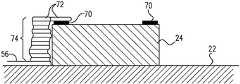
- FIGS. 4A-Care schematic side views of die 24 on substrate 22 , showing successive stages in connection of a circuit trace to contacts 70 on the upper side of the die 24 , in accordance with an embodiment of the invention.
- LIFT station 40deposits successive droplets 72 to create a pillar 74 up to contact 70 , as shown in FIGS. 4B-C .
- the inventorshave created pillars of this sort with widths of 10-20 ⁇ m by building up piles of single droplets 54 .
- positioning assembly 30may move donor substrate 50 away from circuit substrate in order to maintain a sufficient gap between the donor and acceptor surfaces.
- angled LIFT printingin which droplets are ejected from donor film 52 at an oblique (non-perpendicular) angle relative to the surface of substrate 22 , may be applied in order to conformally coat the lateral sides of the die with metal without gaps between the pillar and the die, and thus enhance the mechanical robustness of the traces and connections.
- Angled LIFT printing techniquesthat can be used in this regard are described, for example, in PCT International Publication WO 2016/116921, whose disclosure is incorporated herein by reference.
- Pillar 74takes the place of wire-bonding, which is used to creating this sort of contact in electronic devices that are known in the art.
- the use of LIFT to create such contactsboth enhances robustness of the device against mechanical shock and can reduce overall size, since there is no need to leave space around the components for connection of the wire bonds.
Landscapes
- Engineering & Computer Science (AREA)
- Microelectronics & Electronic Packaging (AREA)
- Computer Hardware Design (AREA)
- Power Engineering (AREA)
- Manufacturing & Machinery (AREA)
- Ceramic Engineering (AREA)
- Physics & Mathematics (AREA)
- Condensed Matter Physics & Semiconductors (AREA)
- General Physics & Mathematics (AREA)
- Manufacturing Of Printed Wiring (AREA)
Abstract
Description
- The present invention relates generally to fabrication of electronic devices, and particularly to methods and apparatus for producing circuits by direct writing of conductive traces on a substrate.
- In laser direct-write (LDW) techniques, a laser beam is used to create a patterned surface with spatially-resolved 3D structures by controlled material ablation or deposition. Laser-induced forward transfer (LIFT) is an LDW technique that can be applied in depositing micro-patterns on a surface.
- In LIFT, laser photons provide the driving force to eject a small volume of material from a donor film toward an acceptor substrate. Typically, the laser beam interacts with the inner side of the donor film, which is coated onto a non-absorbing carrier substrate. The incident laser beam, in other words, propagates through the transparent carrier before the photons are absorbed by the inner surface of the film. Above a certain energy threshold, material is ejected from the donor film toward the surface of the substrate, which is generally placed, in LIFT systems that are known in the art, either in close proximity to or even in contact with the donor film. The applied laser energy can be varied in order to control the thrust of forward propulsion that is generated within the irradiated film volume. Nagel and Lippert survey the principles and applications of LIFT in micro-fabrication in “Laser-Induced Forward Transfer for the Fabrication of Devices,” published inNanomaterials: Processing and Characterization with Lasers,Singh et al., eds. (Wiley-VCH Verlag GmbH & Co. KGaA, 2012), pages 255-316.
- LIFT techniques using metal donor films have been developed for a variety of applications, such as repair of electrical circuits. For example, PCT International Publication WO 2010/100635, whose disclosure is incorporated herein by reference, describes a system and method of repairing electrical circuits in which a laser is used to pre-treat a conductor repair area of a conductor formed on a circuit substrate. The laser beam is applied to a donor substrate in a manner that causes a portion of the donor substrate to be detached therefrom and to be transferred to a predetermined conductor location.
- As another example, PCT International Publication WO 2015/181810, whose disclosure is incorporated herein by reference, describes a method for material deposition using a transparent donor substrate having opposing first and second surfaces and a donor film including a metal formed over the second surface. The donor substrate is positioned in proximity to an acceptor substrate, with the second surface facing toward the acceptor substrate. Pulses of laser radiation are directed to pass through the first surface of the donor substrate and impinge on the donor film so as to induce ejection from the donor film of droplets of molten material onto the acceptor substrate.
- LIFT can be used to print metal traces on a variety of types of substrates. For example, PCT International Publication WO 2016/063270, whose disclosure is incorporated herein by reference, describes a method for metallization using a transparent donor substrate having deposited thereon a donor film including a metal with a thickness less than 2 μm. The donor substrate is positioned in proximity to an acceptor substrate including a semiconductor material with the donor film facing toward the acceptor substrate and with a gap of at least 0.1 mm between the donor film and the acceptor substrate. A train of laser pulses, having a pulse duration less than 2 ns, is directed to impinge on the donor substrate so as to cause droplets of the metal to be ejected from the donor layer and land on the acceptor substrate, thereby forming a circuit trace in ohmic contact with the semiconductor material.
- Embodiments of the present invention that are described hereinbelow provide novel techniques for interconnecting electronic components on a substrate.
- There is therefore provided, in accordance with an embodiment of the invention, a method for producing electronic devices. The method includes fixing a die that includes an electronic component with integral contacts to a dielectric substrate. After fixing the die, a conductive trace is printed over both the dielectric substrate and at least one of the integral contacts, so as to create an ohmic connection between the conductive trace on the dielectric substrate and the electronic component.
- In some embodiments, printing the conductive trace includes ejecting droplets of a conductive material onto both the dielectric substrate and the at least one of the integral contacts. In the disclosed embodiments, ejecting the droplets includes directing a pulsed laser beam to impinge on a donor film including the conductive material, whereby the droplets are ejected by laser-induced forward transfer (LIFT). In one embodiment, ejecting the droplets includes directing the pulsed laser beam so that the droplets are ejected toward the die at an oblique angle relative to a surface of the dielectric substrate. Additionally or alternatively, ejecting the droplets includes directing the pulsed laser beam to impinge on a first donor film including a first metal having a first melting temperature so as to form an adhesion layer on the dielectric substrate along a track of the conductive trace, and then directing the pulsed laser beam to impinge on a second donor film including a second metal having a second melting temperature, higher than the first melting temperature, so as to build up the conductive trace over the adhesion layer.
- Typically, the die has opposing upper and lower sides, wherein the lower side is fixed to the dielectric substrate, and in some embodiments, the at least one of the integral contacts over which the conductive trace is printed is on the upper side. In a disclosed embodiment, ejecting the droplets includes building up a pillar from the ejected droplets alongside the electronic component from the dielectric substrate to the at least one of the integral contacts. Alternatively, the at least one of the integral contacts over which the conductive trace is printed is on one of the lateral sides, between the upper and lower sides.
- In a disclosed embodiment, the method includes, prior to ejecting the droplets, forming an array of holes in the dielectric substrate so as to inhibit recoil of the droplets from the dielectric substrate.
- In one embodiment, the method includes printing adhesive dots on the dielectric substrate by ejecting droplets of an adhesive material onto the dielectric substrate by laser-induced forward transfer (LIFT), wherein fixing the die includes placing the die on the adhesive dots. Additionally or alternatively, the method includes, after the die has been fixed to the dielectric substrate, ejecting droplets of an adhesive material onto the upper side of the die by LIFT.
- In the disclosed embodiments, the conductive trace is printed over a locus on the dielectric substrate along which there was no conductive material prior to fixing the die. In some embodiments, printing the conductive trace includes automatically sensing a location of the at least one of the integral contacts, and printing the conductive trace responsively to the automatically-sensed location.
- In some embodiments, the dielectric substrate includes a flexible foil, which may include a material selected from a group of materials consisting of polymers, papers and fabrics.
- There is also provided, in accordance with an embodiment of the invention, a system for producing electronic devices. The system includes a placement station, which is configured to fix a die, which includes an electronic component with integral contacts, to a dielectric substrate. A printing station is configured to print a conductive trace over both the dielectric substrate and at least one of the integral contacts of the die that has been fixed to the dielectric substrate, so as to create an ohmic connection between the conductive trace on the dielectric substrate and the electronic component.
- The present invention will be more fully understood from the following detailed description of the embodiments thereof, taken together with the drawings in which:
FIG. 1 is schematic side view and block diagram of a system for electronic circuit assembly, in accordance with an embodiment of the present invention;FIGS. 2A-2D are schematic pictorial illustrations showing successive stages in the production of an electronic circuit, in accordance with an embodiment of the invention;FIG. 3 is an image captured by a scanning electron microscope (SEM) of an electronic component assembled into a circuit in accordance with an embodiment of the invention; andFIGS. 4A-C are schematic side views of an electronic component on a substrate, showing successive stages in connection of a circuit trace to the electronic component, in accordance with an embodiment of the invention.- In traditional processes for manufacture of electronic circuits, a pattern of conductive traces is first deposited on a dielectric substrate (such as a rigid or flexible printed circuit substrate). The circuit components, such as semiconductor dies and other active and passive elements, are then fixed to the substrate and connected to the traces, typically by solder or wire bonding. This is the accepted order of operations in circuit manufacture and assembly.
- In modern electronic products, however, there is an increasing demand to integrate electronic circuits onto other sorts of substrates, both rigid and flexible, which may not be compatible with traditional printed circuit technology. For example, some applications call for electronic devices to be mounted and interconnected on flexible substrates, such as plastic foils, paper or fabric. Adapting traditional processes to such substrates can be challenging and costly.
- Embodiments of the present invention that are described herein address this problem by reversing the accepted order of operations: First a die, which includes an electronic component with integral contacts, is fixed to the dielectric substrate, for example by a suitable adhesive. After fixing the die, a conductive trace is printed over both the dielectric substrate and at least one of the integral contacts of the die, thus creating an ohmic connection between the conductive trace on the substrate and the electronic component. Other active and passive components can be fixed to the substrate and interconnected in like manner.
- Conductive traces can be printed in this manner over a locus on the dielectric substrate along which there was no conductive material prior to fixing the die. In other words, the disclosed techniques require only a single process step to perform both deposition of the traces and connection of the traces to the circuit components. To ensure accurate printing of the conductive traces, an automatic sensing system, such as a computer vision system, can be used to sense the locations of the contacts of the die after the die has been fixed to the substrate, and printing of the traces can then be guided to the sensed locations.
- In the disclosed embodiments, the conductive traces are printed using a LIFT process, in which droplets of a conductive material are ejected onto both the dielectric substrate and the integral contacts of the die. (These embodiments assume that the lower side of the die is fixed to the dielectric substrate, and the integral contacts over which the conductive trace is printed are on the upper side or lateral sides of the dies.) As described in detail hereinbelow, LIFT printing of metal droplets is able to overcome large height gaps—on the order of hundreds of microns—between the substrate and the contacts on the upper side of the die, while at the same time producing very fine traces. Such traces may be printed by LIFT with line widths down to 10-20 μm, and may be trimmed (for example, by post-printing laser treatment) to even narrower widths if desired. Furthermore, LIFT printing of metals and highly viscous pastes is relatively indifferent to substrate properties, such as porosity, liquid absorbance and surface energy, and can thus print fine traces with high accuracy even on porous, absorbent substrates such as paper and fabric. This process can be used to create circuits that will afterwards withstand (within limits) bending and stretching of the substrate.
- Alternatively or additionally, however, in some applications, other techniques that are known in the art for direct writing of conductive materials can be applied in creating at least some of the conductive traces.
FIG. 1 is a block diagram and side view of asystem 20 for electronic circuit assembly, in accordance with an embodiment of the invention. In the pictured example, aplacement station 26 places a component, such as asemiconductor die 24, on acircuit substrate 22.Placement station 26 may comprise, for example, a pick-and-place machine, in which arobotic arm 28 places components onsubstrate 22 under instructions from acontrol unit 32 in accordance with a predefined circuit layout. Typically,substrate 22 is mounted on apositioning assembly 30, such as a translation stage, to enablearm 28 to reach all desired locations. The operation ofplacement station 26 differs from pick-and-place machines that are known in the art, however, in that die24 is placed onsubstrate 22 prior to printing of the conductive traces that will subsequently connect to the die.- Optionally, to ensure the accuracy of subsequent operations carried out in
system 20, asensing station 34 detects the actual position at which die24 has been placed onsubstrate 22.Sensing station 34 comprises, for example, acamera 36, which captures images ofsubstrate 22.Control unit 32 processes these images in order to ascertain the exact positions of the components on the substrate. Although sensingstation 34 is shown inFIG. 1 , for the sake of conceptual clarity, as a separate unit, in practice such sensors, such ascamera 36, and sensing functionality may be integrated with the other stations insystem 20. The application ofsensing station 34 insystem 20 is particularly advantageous in overcoming the limited accuracy of pick-and-place tools that are known in the art, as well as possible distortions that may occur in the shape of a flexible substrate in the course of the assembly process. Precise sensing of the positions ofdie 24 and other components enables accurate printing of very fine interconnecting traces (for example, with widths of 20 μm or less) after the components have been fixed tosubstrate 22. - More generally speaking,
control unit 32 may adapt the traces that are to be printed depending on the actual positions of the dies in relation to other circuit components. This sort of adaptation is particularly useful, for example, when there is high density of circuit components or many input/output pins on a given die, as well as narrow lines, one should take into consideration the final (actual) position of the die in relation to the rest of the circuit. In such cases,control unit 32 selects the trace locations so as to conform with electrical design rules and avoid circuit defects. This approach can be used in creating circuits with component density as great as or even greater than is achievable using conventional manufacturing processes. - Depending on the material properties of
substrate 22, asurface preparation station 38 can be used to treat the surface of thesubstrate 22 in order to enhance adhesion of the traces thereon. For example, when the surface is very smooth,surface preparation station 38 may create arrays of small holes in the surface, typically several microns deep and several microns across, which will roughen the surface and reduce the recoil of metal droplets from the surface in the subsequent LIFT printing stage. The holes may be made specifically in the loci of the conductive traces that are to be printed onsubstrate 22, or alternatively over wider areas of thesubstrate 22. The holes may be drilled by a laser, for example, or impressed mechanically in the surface of thesubstrate 22. - A printing station, for example a
LIFT station 40, prints conductive traces56 onsubstrate 22, in ohmic connection with the contact pads ondie 24.LIFT station 40 comprises anoptical assembly 41, in which alaser 42 emits pulsed radiation.Optics 46focus laser beam 48 onto atransparent donor substrate 50 having at least onedonor film 52 deposited thereon. Positioningassembly 30positions donor substrate 50 and/orcircuit substrate 22 so that thedonor substrate 50 is in proximity to the upper surface of the acceptor substrate, withdonor film 52 facing toward the circuit substrate and a small gap in between (typically no more than a few hundred microns, and possibly less). Although positioningassembly 30 is shown inFIG. 1 , for the sake of simplicity, as a basic X-Y-Z stage belowcircuit substrate 22, in practice the positioningassembly 30 inLIFT station 40 additionally or alternatively may be capable of positioning donor substrate and/or elements ofoptical assembly 41, as will be apparent to those skilled in the art. Donor substrate 50 typically comprises a glass or plastic sheet or other suitable transparent material, whiledonor film 52 comprises a suitable donor material, such as one or more pure metals and/or metal alloys. Typically, the thickness of the donor films is no more than a few microns.Optics 46focus beam 48 to pass through the outer surface ofdonor substrate 50 and to impinge ondonor film 52, thereby causingdroplets 54 of a fluid to be ejected fromdonor film 52 and fly across the gap to land oncircuit substrate 22. The fluid comprises a molten form of the material indonor film 52, which then hardens on the acceptor surface to form solid pieces having a shape defined by the printing pattern. Ascanner 44, such as a rotating mirror and/or an acousto-optic beam deflector under control ofcontrol unit 32,scans laser beam 48 so as to irradiate different spots ondonor film 52 and thus createconductive traces 56 in the appropriate locations oncircuit substrate 22.Laser 42 comprises, for example, a pulsed Nd:YAG laser with frequency-doubled output, which permits the pulse amplitude to be controlled conveniently bycontrol unit 32. Typically,control unit 32 comprises a general-purpose computer, with suitable interfaces for controlling and receiving feedback fromoptical assembly 41, positioningassembly 30, and other elements ofsystem 20. The inventors have found that for good LIFT deposition results, the optimal pulse duration is in the range of 0.1 ns to 1 ns, but longer or shorter pulses may be used, depending on application requirements.Optics 46 are similarly controllable in order to adjust the size of the focal spot formed by the laser beam ondonor film 52.- The size of
droplets 54 is determined, inter alia, by the laser pulse energy, duration, and focal spot size and the thickness of the donor film. The above-mentioned PCT International Publication 2015/181810, for example, describes LIFT techniques and parameters that can be applied so that each laser pulse causes a single, relatively large droplet to be ejected from the donor film. These techniques and parameters can be applied advantageously inLIFT station 40, since the droplets are ejected towardcircuit substrate 22 with accurate directionality, making it possible to holddonor film 52 at a distance of at least 100 μm from the acceptor substrate during ejection of the droplets and to create the desired structures with precision. - In some embodiments,
LIFT station 40 causesdroplets 54 of two or more different fluids, having different compositions, to be ejected fromdifferent donor films 52. For example, the different fluids can be ejected by directingbeam 48 fromlaser 42 to impinge on different areas of donor films52 (either on thesame donor substrate 50 or different donor substrates) containing different materials. The different fluids may be ejected sequentially toward the same location oncircuit substrate 22 and/or toward different locations, in order to print the desired traces56. - For example, to enhance adhesion of
traces 56 to certain types of circuit substrates, such as polymer substrates, afirst donor film 52 comprising a metal with a low melting temperature, such as tin or a tin alloy, is used in printing an initial adhesion layer along the loci of the traces. The low-temperature metal droplets cool quickly while at the same time locally melting the polymer, thus forming a layer to which subsequent laser droplets with higher temperature and energy will readily adhere. (This adhesion layer need not be dense or fully coat the substrate. A low-density adhesion layer, covering no more than 20-30% of the intended area oftrace 56, is often sufficient to anchor the subsequent structural layer.) Thereafter, asecond donor film 52 with a structural metal, such as copper (and/or aluminum or nickel, for example) is printed over the adhesion layer in order to reach the desired dimensions, connectivity and conductivity of the trace. As noted earlier,control unit 32controls scanner 44 and other elements ofoptical assembly 41 so as to write donor material fromfilms 52 to the appropriate locations oncircuit substrate 22 and to make multiple passes, as needed, in order to build up the deposited volume of the donor material to the desired thickness. FIGS. 2A-2D are schematic pictorial illustrations showing successive stages in the production of an electronic circuit, in accordance with an embodiment of the invention. As a preliminary step, shown inFIG. 2A ,substrate 22 is coated with anadhesive layer 60 or, alternatively, a suitable pattern of adhesive, such as an array of adhesive dots (not shown), which may also be printed by a LIFT process. (LIFT printing of adhesive may also be used in printing dots of adhesive, when needed, on top ofdie 24 and other circuit components.)Die 24 is then fixed in position, for example byplacement station 26, with the lower side of the die24 resting onadhesive layer 60, as illustrated inFIG. 2B . After all components have been placed onsubstrate 22,adhesive layer 60 may be cured (for example by application of ultraviolet radiation or heat) in order to hold the components securely in place.- When necessary,
surface preparation station 38 preparestracks 62 onsubstrate 22, as shown inFIG. 2C , over which traces56 will subsequently be printed. As explained earlier, such preparation is advantageous for materials that are not inherently sufficiently rough to capture and hold the droplets printed byLIFT station 40.Tracks 62 may contain, for example, an array of shallow holes with a diameter that is one to two times the diameter ofdroplets 54 and depth of roughly 3-6 μm. Alternatively or additionally, LIFT station may be operated to create an initial metal adhesion layer, as explained above. On the other hand, surface preparation before LIFT printing may not be needed on substrate materials that are sufficiently porous. - Finally,
conductive trace 56 is printed byLIFT station 40 over bothsubstrate 22 and the integral contacts on the upper side ofdie 24, as shown inFIG. 2D .Trace 56 is built up over the edges ofdie 24 in order to connect with the contacts of the die. (Details of an implementation of this latter step are shown inFIGS. 4A-C .) AlthoughLIFT station 40 is capable of printing very fine traces, as explained above, in some cases wider and/or thicker conductive traces may be printed in order to sink heat away from the circuit components in operation. FIG. 3 is an image captured by a scanning electron microscope (SEM) of anactual die 24 assembled ontosubstrate 22 in accordance with an embodiment of the invention.Substrate 22 in this example is a polyethylene terephthalate (PET) foil, while die24 comprises an LED in a surface-mount package.Traces 56 are built up from LIFT droplets and extend over the “shoulders” of the die to reach the contact pads on the upper side. Application of a suitable voltage betweentraces 56 on the opposing sides ofdie 24 caused the LED to emit light.FIGS. 4A-C are schematic side views of die24 onsubstrate 22, showing successive stages in connection of a circuit trace tocontacts 70 on the upper side of the die24, in accordance with an embodiment of the invention. After initial placement ofdie 24, as shown inFIG. 4A ,LIFT station 40 depositssuccessive droplets 72 to create apillar 74 up to contact70, as shown inFIGS. 4B-C . The inventors have created pillars of this sort with widths of 10-20 μm by building up piles ofsingle droplets 54. As the height ofpillar 74 grows, positioningassembly 30 may movedonor substrate 50 away from circuit substrate in order to maintain a sufficient gap between the donor and acceptor surfaces.- It is desirable to build a small tilt into the pillar (on the order of 3°) to prevent gaps from opening between the pillar and the die contacts. Additionally or alternatively, angled LIFT printing, in which droplets are ejected from
donor film 52 at an oblique (non-perpendicular) angle relative to the surface ofsubstrate 22, may be applied in order to conformally coat the lateral sides of the die with metal without gaps between the pillar and the die, and thus enhance the mechanical robustness of the traces and connections. Angled LIFT printing techniques that can be used in this regard are described, for example, in PCT International Publication WO 2016/116921, whose disclosure is incorporated herein by reference. Pillar 74 takes the place of wire-bonding, which is used to creating this sort of contact in electronic devices that are known in the art. The use of LIFT to create such contacts both enhances robustness of the device against mechanical shock and can reduce overall size, since there is no need to leave space around the components for connection of the wire bonds.- Although the examples shown in the figures and described above relate to particular types of components, the principles of the present invention may be applied in assembling circuits comprising a wide variety of different sorts of components, including (but not limited to):
- Semiconductor dies.
- Active devices, such as batteries, photovoltaics, sensors, optoelectronics, thin-film devices, and MEMS devices.
- Pre-assembled hybrid devices, such as rigid or flexible foils with components already mounted on them.
- Surface-mount devices, such as discrete transistors, capacitors, inductors and resistors.
- It will thus be appreciated that the embodiments described above are cited by way of example, and that the present invention is not limited to what has been particularly shown and described hereinabove. Rather, the scope of the present invention includes both combinations and subcombinations of the various features described hereinabove, as well as variations and modifications thereof which would occur to persons skilled in the art upon reading the foregoing description and which are not disclosed in the prior art.
Claims (30)
Priority Applications (1)
| Application Number | Priority Date | Filing Date | Title |
|---|---|---|---|
| US16/495,112US11881466B2 (en) | 2017-05-24 | 2018-04-26 | Electrical interconnection of circuit elements on a substrate without prior patterning |
Applications Claiming Priority (3)
| Application Number | Priority Date | Filing Date | Title |
|---|---|---|---|
| US201762510286P | 2017-05-24 | 2017-05-24 | |
| US16/495,112US11881466B2 (en) | 2017-05-24 | 2018-04-26 | Electrical interconnection of circuit elements on a substrate without prior patterning |
| PCT/IL2018/050455WO2018216002A1 (en) | 2017-05-24 | 2018-04-26 | Electrical interconnection of circuit elements on a substrate without prior patterning |
Publications (2)
| Publication Number | Publication Date |
|---|---|
| US20210028141A1true US20210028141A1 (en) | 2021-01-28 |
| US11881466B2 US11881466B2 (en) | 2024-01-23 |
Family
ID=64395438
Family Applications (1)
| Application Number | Title | Priority Date | Filing Date |
|---|---|---|---|
| US16/495,112Active2039-03-11US11881466B2 (en) | 2017-05-24 | 2018-04-26 | Electrical interconnection of circuit elements on a substrate without prior patterning |
Country Status (6)
| Country | Link |
|---|---|
| US (1) | US11881466B2 (en) |
| JP (1) | JP2020521331A (en) |
| KR (1) | KR20200010208A (en) |
| CN (1) | CN110637354B (en) |
| TW (1) | TW201901887A (en) |
| WO (1) | WO2018216002A1 (en) |
Cited By (9)
| Publication number | Priority date | Publication date | Assignee | Title |
|---|---|---|---|---|
| US20220248540A1 (en)* | 2021-01-29 | 2022-08-04 | Orbotech Ltd. | High-resolution soldering |
| US11446750B2 (en) | 2020-02-03 | 2022-09-20 | Io Tech Group Ltd. | Systems for printing solder paste and other viscous materials at high resolution |
| US11497124B2 (en)* | 2020-06-09 | 2022-11-08 | Io Tech Group Ltd. | Methods for printing conformal materials on component edges at high resolution |
| US11622451B2 (en) | 2020-02-26 | 2023-04-04 | Io Tech Group Ltd. | Systems and methods for solder paste printing on components |
| US11691332B2 (en) | 2020-08-05 | 2023-07-04 | Io Tech Group Ltd. | Systems and methods for 3D printing with vacuum assisted laser printing machine |
| US20240084457A1 (en)* | 2022-09-09 | 2024-03-14 | Hamilton Sundstrand Corporation | Expansive coatings for anchoring to composite substrates |
| US12046575B2 (en) | 2019-05-01 | 2024-07-23 | Io Tech Group Ltd. | Method to electrically connect chip with top connectors using 3D printing |
| US12089343B2 (en)* | 2022-09-01 | 2024-09-10 | Reophotonics, Ltd. | Methods for printing a conductive pillar with high precision |
| WO2025008267A1 (en)* | 2023-07-05 | 2025-01-09 | Zf Friedrichshafen Ag | Adhering lamella packets using lift technology |
Families Citing this family (3)
| Publication number | Priority date | Publication date | Assignee | Title |
|---|---|---|---|---|
| EP3852132A1 (en) | 2020-01-20 | 2021-07-21 | Infineon Technologies Austria AG | Additive manufacturing of a frontside or backside interconnect of a semiconductor die |
| KR102668012B1 (en)* | 2020-06-04 | 2024-05-21 | 오르보테크 엘티디. | High resolution soldering |
| CN114126248B (en)* | 2022-01-21 | 2022-05-24 | 深圳原驰三维技术有限公司 | Printed circuit board pad and circuit defect repairing method |
Citations (2)
| Publication number | Priority date | Publication date | Assignee | Title |
|---|---|---|---|---|
| US20090068790A1 (en)* | 2007-09-07 | 2009-03-12 | Vertical Circuits, Inc. | Electrical Interconnect Formed by Pulsed Dispense |
| WO2016116921A1 (en)* | 2015-01-21 | 2016-07-28 | Orbotech Ltd. | Angled lift jetting |
Family Cites Families (154)
| Publication number | Priority date | Publication date | Assignee | Title |
|---|---|---|---|---|
| US3963852A (en) | 1973-08-04 | 1976-06-15 | Moore Business Forms, Inc. | Clay-coated record material of improved image durability |
| JPS61260603A (en) | 1985-05-14 | 1986-11-18 | 三菱電機株式会社 | Electronic component |
| US4752455A (en) | 1986-05-27 | 1988-06-21 | Kms Fusion, Inc. | Pulsed laser microfabrication |
| US4891183A (en) | 1986-12-03 | 1990-01-02 | Chrysler Motors Corporation | Method of preparing alloy compositions |
| US4970196A (en) | 1987-01-15 | 1990-11-13 | The Johns Hopkins University | Method and apparatus for the thin film deposition of materials with a high power pulsed laser |
| US4931323A (en) | 1987-12-10 | 1990-06-05 | Texas Instruments Incorporated | Thick film copper conductor patterning by laser |
| US4895735A (en) | 1988-03-01 | 1990-01-23 | Texas Instruments Incorporated | Radiation induced pattern deposition |
| US4977038A (en) | 1989-04-14 | 1990-12-11 | Karl Sieradzki | Micro- and nano-porous metallic structures |
| US4987006A (en) | 1990-03-26 | 1991-01-22 | Amp Incorporated | Laser transfer deposition |
| US5173441A (en) | 1991-02-08 | 1992-12-22 | Micron Technology, Inc. | Laser ablation deposition process for semiconductor manufacture |
| JPH04269801A (en) | 1991-02-25 | 1992-09-25 | Juichiro Ozawa | Material for forming resistor film |
| US5292559A (en) | 1992-01-10 | 1994-03-08 | Amp Incorporated | Laser transfer process |
| JPH0634283A (en) | 1992-06-16 | 1994-02-08 | Ishikawajima Harima Heavy Ind Co Ltd | How to make a space heat exchanger |
| US5420611A (en) | 1992-06-29 | 1995-05-30 | Eastman Kodak Company | Apparatus and method for eliminating feedback noise in laser thermal printing |
| DE4232373A1 (en) | 1992-09-03 | 1994-03-10 | Deutsche Forsch Luft Raumfahrt | Structural semiconductor layer deposition method - heating applied film using laser beam, to transfer the film material to surface of substrate |
| DE4229399C2 (en) | 1992-09-03 | 1999-05-27 | Deutsch Zentr Luft & Raumfahrt | Method and device for producing a functional structure of a semiconductor component |
| US5308737A (en) | 1993-03-18 | 1994-05-03 | Minnesota Mining And Manufacturing Company | Laser propulsion transfer using black metal coated substrates |
| US5683601A (en) | 1994-10-24 | 1997-11-04 | Panasonic Technologies, Inc. | Laser ablation forward metal deposition with electrostatic assisted bonding |
| CN1316835C (en) | 1994-11-04 | 2007-05-16 | 安德鲁公司 | Antenna control system |
| US5935758A (en) | 1995-04-20 | 1999-08-10 | Imation Corp. | Laser induced film transfer system |
| WO1998041189A1 (en) | 1997-03-20 | 1998-09-24 | Therics, Inc. | Fabrication of tissue products using a mold formed by solid free-form methods |
| US6025110A (en) | 1997-09-18 | 2000-02-15 | Nowak; Michael T. | Method and apparatus for generating three-dimensional objects using ablation transfer |
| US6159832A (en) | 1998-03-18 | 2000-12-12 | Mayer; Frederick J. | Precision laser metallization |
| JP3871096B2 (en) | 1998-05-21 | 2007-01-24 | 株式会社ティラド | Combined integrated heat exchanger of evaporator, absorber and subcooler, and manufacturing method thereof |
| US6155330A (en) | 1998-11-04 | 2000-12-05 | Visteon Global Technologies, Inc. | Method of spray forming metal deposits using a metallic spray forming pattern |
| US6805918B2 (en) | 1999-01-27 | 2004-10-19 | The United States Of America As Represented By The Secretary Of The Navy | Laser forward transfer of rheological systems |
| US6815015B2 (en) | 1999-01-27 | 2004-11-09 | The United States Of America As Represented By The Secretary Of The Navy | Jetting behavior in the laser forward transfer of rheological systems |
| US6177151B1 (en) | 1999-01-27 | 2001-01-23 | The United States Of America As Represented By The Secretary Of The Navy | Matrix assisted pulsed laser evaporation direct write |
| US6348295B1 (en) | 1999-03-26 | 2002-02-19 | Massachusetts Institute Of Technology | Methods for manufacturing electronic and electromechanical elements and devices by thin-film deposition and imaging |
| US6792326B1 (en) | 1999-05-24 | 2004-09-14 | Potomac Photonics, Inc. | Material delivery system for miniature structure fabrication |
| US6583381B1 (en) | 1999-05-24 | 2003-06-24 | Potomac Photonics, Inc. | Apparatus for fabrication of miniature structures |
| US6440503B1 (en) | 2000-02-25 | 2002-08-27 | Scimed Life Systems, Inc. | Laser deposition of elements onto medical devices |
| US6649861B2 (en) | 2000-05-24 | 2003-11-18 | Potomac Photonics, Inc. | Method and apparatus for fabrication of miniature structures |
| ES2296659T3 (en) | 2000-09-25 | 2008-05-01 | Voxeljet Technology Gmbh | PROCEDURE FOR THE MANUFACTURE OF AN ELEMENT WITH THE DEPOSITION TECHNIQUE. |
| DE10062683A1 (en) | 2000-12-15 | 2002-06-20 | Heidelberger Druckmasch Ag | Multi-beam scanning device for recording apparatus has acousto-optical deflector or modulator that co-rotates with deflection element |
| US6412143B1 (en) | 2001-01-08 | 2002-07-02 | Cheng-Lu Chen | Structure of material for forming a stop at an end of lashing string |
| US7087200B2 (en) | 2001-06-22 | 2006-08-08 | The Regents Of The University Of Michigan | Controlled local/global and micro/macro-porous 3D plastic, polymer and ceramic/cement composite scaffold fabrication and applications thereof |
| GB2379083A (en) | 2001-08-20 | 2003-02-26 | Seiko Epson Corp | Inkjet printing on a substrate using two immiscible liquids |
| WO2003026368A1 (en) | 2001-09-11 | 2003-03-27 | Daiken Chemical Co., Ltd. | Method for forming image on object surface including circuit substrate |
| SG122749A1 (en) | 2001-10-16 | 2006-06-29 | Inst Data Storage | Method of laser marking and apparatus therefor |
| GR1004059B (en) | 2001-12-31 | 2002-11-15 | Ιωαννα Ζεργιωτη | Fabrication of biopolymer patterns by means of laser transfer |
| US7188492B2 (en) | 2002-01-18 | 2007-03-13 | Linde Aktiengesellschaft | Plate heat exchanger |
| DE10210146A1 (en) | 2002-03-07 | 2003-09-25 | Aurentum Innovationstechnologi | Quality printing process and printing machine, as well as a print audit for this |
| US7316748B2 (en) | 2002-04-24 | 2008-01-08 | Wisconsin Alumni Research Foundation | Apparatus and method of dispensing small-scale powders |
| DE10237732B4 (en) | 2002-08-17 | 2004-08-26 | BLZ Bayerisches Laserzentrum Gemeinnützige Forschungsgesellschaft mbH | Laser beam marking method and marking device for laser beam marking of a target substrate |
| US6921626B2 (en) | 2003-03-27 | 2005-07-26 | Kodak Polychrome Graphics Llc | Nanopastes as patterning compositions for electronic parts |
| US6873398B2 (en) | 2003-05-21 | 2005-03-29 | Esko-Graphics A/S | Method and apparatus for multi-track imaging using single-mode beams and diffraction-limited optics |
| US6899988B2 (en) | 2003-06-13 | 2005-05-31 | Kodak Polychrome Graphics Llc | Laser thermal metallic donors |
| US7277770B2 (en) | 2003-07-15 | 2007-10-02 | Huang Wen C | Direct write process and apparatus |
| US7682970B2 (en) | 2003-07-16 | 2010-03-23 | The Regents Of The University Of California | Maskless nanofabrication of electronic components |
| US7423286B2 (en) | 2003-09-05 | 2008-09-09 | Si2 Technologies, Inc. | Laser transfer article and method of making |
| US7521651B2 (en) | 2003-09-12 | 2009-04-21 | Orbotech Ltd | Multiple beam micro-machining system and method |
| US20050095367A1 (en) | 2003-10-31 | 2005-05-05 | Babiarz Alec J. | Method of noncontact dispensing of viscous material |
| US7540996B2 (en) | 2003-11-21 | 2009-06-02 | The Boeing Company | Laser sintered titanium alloy and direct metal fabrication method of making the same |
| US7294449B1 (en) | 2003-12-31 | 2007-11-13 | Kovio, Inc. | Radiation patternable functional materials, methods of their use, and structures formed therefrom |
| US8535041B2 (en) | 2006-07-28 | 2013-09-17 | Microcontinuum, Inc. | Addressable flexible patterns |
| CN103646848B (en) | 2004-06-04 | 2018-06-05 | 伊利诺伊大学评议会 | The method of assembling printable semiconductor elements and manufacture electronic device |
| US8217381B2 (en) | 2004-06-04 | 2012-07-10 | The Board Of Trustees Of The University Of Illinois | Controlled buckling structures in semiconductor interconnects and nanomembranes for stretchable electronics |
| US7799699B2 (en) | 2004-06-04 | 2010-09-21 | The Board Of Trustees Of The University Of Illinois | Printable semiconductor structures and related methods of making and assembling |
| US7236334B2 (en) | 2004-08-31 | 2007-06-26 | Hitachi Global Storage Technologies Netherlands B.V. | Repeatable ESD protection utilizing a process for unshorting a first shorting material between electrical pads and reshorting by recreating the short |
| WO2006033822A2 (en) | 2004-09-07 | 2006-03-30 | Massachusetts Institute Of Technology | Fabrication of electronic and photonic systems on flexible substrates by layer transfer method |
| US8216931B2 (en) | 2005-03-31 | 2012-07-10 | Gang Zhang | Methods for forming multi-layer three-dimensional structures |
| US7358169B2 (en) | 2005-04-13 | 2008-04-15 | Hewlett-Packard Development Company, L.P. | Laser-assisted deposition |
| US7396631B2 (en) | 2005-10-07 | 2008-07-08 | 3M Innovative Properties Company | Radiation curable thermal transfer elements |
| US7784173B2 (en) | 2005-12-27 | 2010-08-31 | Palo Alto Research Center Incorporated | Producing layered structures using printing |
| US9327056B2 (en) | 2006-02-14 | 2016-05-03 | Washington State University | Bone replacement materials |
| US20070224235A1 (en) | 2006-03-24 | 2007-09-27 | Barron Tenney | Medical devices having nanoporous coatings for controlled therapeutic agent delivery |
| US7608308B2 (en) | 2006-04-17 | 2009-10-27 | Imra America, Inc. | P-type semiconductor zinc oxide films process for preparation thereof, and pulsed laser deposition method using transparent substrates |
| TWI431380B (en) | 2006-05-12 | 2014-03-21 | Photon Dynamics Inc | Deposition repair apparatus and methods |
| TWI348338B (en) | 2006-05-24 | 2011-09-01 | Unimicron Technology Corp | Method for repairing the circuitry of circuit board |
| US20080006966A1 (en) | 2006-07-07 | 2008-01-10 | Stratasys, Inc. | Method for building three-dimensional objects containing metal parts |
| US7569832B2 (en) | 2006-07-14 | 2009-08-04 | Carestream Health, Inc. | Dual-screen digital radiographic imaging detector array |
| US7935242B2 (en) | 2006-08-21 | 2011-05-03 | Micron Technology, Inc. | Method of selectively removing conductive material |
| US20080099515A1 (en) | 2006-10-11 | 2008-05-01 | Nordson Corporation | Thin line conformal coating apparatus and method |
| US8420978B2 (en) | 2007-01-18 | 2013-04-16 | The Board Of Trustees Of The University Of Illinois | High throughput, low cost dual-mode patterning method for large area substrates |
| US20080233291A1 (en) | 2007-03-23 | 2008-09-25 | Chandrasekaran Casey K | Method for depositing an inorganic layer to a thermal transfer layer |
| US10231344B2 (en) | 2007-05-18 | 2019-03-12 | Applied Nanotech Holdings, Inc. | Metallic ink |
| WO2008157666A1 (en) | 2007-06-19 | 2008-12-24 | The Government Of The United States Of America, As Represented By The Secretary Of The Navy | Sub-micron laser direct write |
| WO2009018340A2 (en) | 2007-07-31 | 2009-02-05 | Boston Scientific Scimed, Inc. | Medical device coating by laser cladding |
| US20090061112A1 (en) | 2007-08-27 | 2009-03-05 | Mu-Gahat Enterprises, Llc | Laser circuit etching by subtractive deposition |
| US8728589B2 (en) | 2007-09-14 | 2014-05-20 | Photon Dynamics, Inc. | Laser decal transfer of electronic materials |
| US7534544B2 (en) | 2007-10-19 | 2009-05-19 | E.I. Du Pont De Nemours And Company | Method of separating an exposed thermal transfer assemblage |
| GB2453774B (en) | 2007-10-19 | 2013-02-20 | Materials Solutions | A method of making an article |
| US20090130427A1 (en) | 2007-10-22 | 2009-05-21 | The Regents Of The University Of California | Nanomaterial facilitated laser transfer |
| US7938855B2 (en) | 2007-11-02 | 2011-05-10 | Boston Scientific Scimed, Inc. | Deformable underlayer for stent |
| DE102007055019B4 (en) | 2007-11-14 | 2019-04-04 | Fraunhofer-Gesellschaft zur Förderung der angewandten Forschung e.V. | Method for producing a nanoporous layer |
| TWI375498B (en) | 2007-11-21 | 2012-10-21 | Ind Tech Res Inst | High perfromance laser-assisted transferring system and transfer component |
| TW200945339A (en) | 2007-12-19 | 2009-11-01 | Koninkl Philips Electronics Nv | Optical disk format for direct writing materials on a substrate |
| WO2009087638A2 (en) | 2008-01-10 | 2009-07-16 | Orbotech Ltd. | Multiple mirror calibration system |
| US8056222B2 (en) | 2008-02-20 | 2011-11-15 | The United States Of America, As Represented By The Secretary Of The Navy | Laser-based technique for the transfer and embedding of electronic components and devices |
| US8215371B2 (en) | 2008-04-18 | 2012-07-10 | Stratasys, Inc. | Digital manufacturing with amorphous metallic alloys |
| EP2299784A4 (en) | 2008-06-16 | 2012-05-30 | Toray Industries | CONTOUR MODELING METHOD, DEVICE MANUFACTURING METHOD USING THE CONTOUR MODELING METHOD, AND DEVICE |
| US9616524B2 (en) | 2008-06-19 | 2017-04-11 | Utilight Ltd. | Light induced patterning |
| US7942987B2 (en) | 2008-06-24 | 2011-05-17 | Stratasys, Inc. | System and method for building three-dimensional objects with metal-based alloys |
| JP2011529126A (en) | 2008-07-24 | 2011-12-01 | コヴィオ インコーポレイテッド | Aluminum ink and method for producing the same, method for depositing aluminum ink, and film formed by printing and / or depositing aluminum ink |
| US20100021638A1 (en) | 2008-07-28 | 2010-01-28 | Solidscape, Inc. | Method for fabricating three dimensional models |
| WO2010032224A2 (en) | 2008-09-22 | 2010-03-25 | Asml Netherlands B.V. | Lithographic apparatus, programmable patterning device and lithographic method |
| JP2010098526A (en) | 2008-10-16 | 2010-04-30 | Sony Corp | Receiving apparatus, content receiving method, and program |
| IL197349A0 (en) | 2009-03-02 | 2009-12-24 | Orbotech Ltd | A method and system for electrical circuit repair |
| US8663754B2 (en) | 2009-03-09 | 2014-03-04 | Imra America, Inc. | Pulsed laser micro-deposition pattern formation |
| US20120025182A1 (en) | 2009-04-03 | 2012-02-02 | Sharp Kabushiki Kaisha | Donor substrate, process for production of transfer film, and process for production of organic electroluminescent element |
| DE102009020774B4 (en) | 2009-05-05 | 2011-01-05 | Universität Stuttgart | Method for contacting a semiconductor substrate |
| US8262916B1 (en) | 2009-06-30 | 2012-09-11 | Microfabrica Inc. | Enhanced methods for at least partial in situ release of sacrificial material from cavities or channels and/or sealing of etching holes during fabrication of multi-layer microscale or millimeter-scale complex three-dimensional structures |
| US8129088B2 (en) | 2009-07-02 | 2012-03-06 | E.I. Du Pont De Nemours And Company | Electrode and method for manufacturing the same |
| US20110136162A1 (en) | 2009-08-31 | 2011-06-09 | Drexel University | Compositions and Methods for Functionalized Patterning of Tissue Engineering Substrates Including Bioprinting Cell-Laden Constructs for Multicompartment Tissue Chambers |
| US8743165B2 (en) | 2010-03-05 | 2014-06-03 | Micronic Laser Systems Ab | Methods and device for laser processing |
| US20130029480A1 (en) | 2010-04-09 | 2013-01-31 | Frank Niklaus | Free form printing of silicon micro- and nanostructures |
| GB201009847D0 (en) | 2010-06-11 | 2010-07-21 | Dzp Technologies Ltd | Deposition method, apparatus, printed object and uses |
| KR101114256B1 (en) | 2010-07-14 | 2012-03-05 | 한국과학기술원 | Method of fabricating pattern |
| GB201019579D0 (en) | 2010-11-19 | 2010-12-29 | Lingvitae Holding As | Method and apparatus for direct writing |
| JP2012190877A (en) | 2011-03-09 | 2012-10-04 | Fujifilm Corp | Nanoimprint method and nanoimprint device for use therein |
| TW201238738A (en) | 2011-03-25 | 2012-10-01 | Hon Hai Prec Ind Co Ltd | Products shell manufacturing method and structure |
| US20120247740A1 (en) | 2011-03-31 | 2012-10-04 | Denso International America, Inc. | Nested heat exchangers |
| US8815345B2 (en) | 2011-05-26 | 2014-08-26 | Solidscape, Inc. | Method for fabricating three dimensional models |
| WO2013010108A1 (en) | 2011-07-13 | 2013-01-17 | Nuvotronics, Llc | Methods of fabricating electronic and mechanical structures |
| US9034674B2 (en) | 2011-08-08 | 2015-05-19 | Quarkstar Llc | Method and apparatus for coupling light-emitting elements with light-converting material |
| KR101616761B1 (en) | 2011-08-16 | 2016-04-29 | 에이에스엠엘 네델란즈 비.브이. | Lithographic apparatus, programmable patterning device and lithographic method |
| EP2751081B1 (en) | 2011-09-12 | 2017-01-04 | Farma GRS, d.o.o. | Polymorphic form of pitavastatin calcium |
| RU2539135C2 (en) | 2012-02-27 | 2015-01-10 | Юрий Александрович Чивель | Production of 3d articles of powders and device to this end |
| WO2013124114A1 (en) | 2012-02-23 | 2013-08-29 | Asml Netherlands B.V. | Device, lithographic apparatus, method for guiding radiation and device manufacturing method |
| DE102012003866B4 (en) | 2012-02-23 | 2013-07-25 | Universität Stuttgart | Method for contacting a semiconductor substrate, in particular for contacting solar cells, and solar cells |
| EP2660352A1 (en) | 2012-05-02 | 2013-11-06 | Nederlandse Organisatie voor toegepast -natuurwetenschappelijk onderzoek TNO | Donor sheet and method for light induced forward transfer manufacturing |
| WO2013168223A1 (en)* | 2012-05-08 | 2013-11-14 | 富士機械製造株式会社 | Semiconductor package and method for manufacturing same |
| GB2501918B (en) | 2012-05-11 | 2014-06-18 | Rolls Royce Plc | Casing |
| US9044805B2 (en) | 2012-05-16 | 2015-06-02 | Apple Inc. | Layer-by-layer construction with bulk metallic glasses |
| US9943996B2 (en) | 2012-05-22 | 2018-04-17 | University Of Southern California | Process planning of meniscus shapes for fabricating smooth surfaces in mask image projection based additive manufacturing |
| US9090095B2 (en) | 2012-06-04 | 2015-07-28 | Micronic Mydata AB | Optical writer for flexible foils |
| US11376349B2 (en) | 2012-10-05 | 2022-07-05 | University of Pittsburgh—of the Commonwealth System of Higher Education | Biodegradable iron-containing compositions, methods of preparing and applications therefor |
| US9446618B2 (en) | 2012-10-21 | 2016-09-20 | Photon Jet Ltd | Multi-technology printing system |
| ES2471568B1 (en) | 2012-11-22 | 2015-08-21 | Abengoa Solar New Technologies S.A. | Procedure for creating electrical contacts and contacts thus created |
| CN105122135B (en) | 2013-02-12 | 2020-03-20 | 卡本有限公司 | Continuous liquid mesophase printing |
| JP2016516211A (en) | 2013-02-18 | 2016-06-02 | オルボテック リミテッド | Two-step direct writing laser metallization |
| US9249015B2 (en) | 2013-02-27 | 2016-02-02 | International Business Machines Corporation | Mold for forming complex 3D MEMS components |
| US9192999B2 (en) | 2013-07-01 | 2015-11-24 | General Electric Company | Methods and systems for electrochemical machining of an additively manufactured component |
| US9029058B2 (en) | 2013-07-17 | 2015-05-12 | Stratasys, Inc. | Soluble support material for electrophotography-based additive manufacturing |
| US9023566B2 (en) | 2013-07-17 | 2015-05-05 | Stratasys, Inc. | ABS part material for electrophotography-based additive manufacturing |
| US20150024317A1 (en) | 2013-07-17 | 2015-01-22 | Stratasys, Inc. | High-Performance Consumable Materials for Electrophotography-Based Additive Manufacturing |
| KR102279622B1 (en) | 2013-10-14 | 2021-07-20 | 오르보테크 엘티디. | LIFT printing of multi-composition material structures |
| JP6665386B2 (en) | 2013-12-15 | 2020-03-13 | オーボテック リミテッド | Repair of printed circuit wiring |
| US20150197063A1 (en) | 2014-01-12 | 2015-07-16 | Zohar SHINAR | Device, method, and system of three-dimensional printing |
| WO2015106193A1 (en) | 2014-01-13 | 2015-07-16 | Kevin Engel | Additive metal deposition process |
| US9840789B2 (en) | 2014-01-20 | 2017-12-12 | City University Of Hong Kong | Etching in the presence of alternating voltage profile and resulting porous structure |
| IL247946B (en) | 2014-04-10 | 2022-08-01 | Orbotech Ltd | Metallization using direct writing with a pulsed laser |
| CN106414791A (en) | 2014-05-27 | 2017-02-15 | 奥博泰克有限公司 | Printing of 3D structures by laser-induced forward transfer |
| US9925797B2 (en) | 2014-08-07 | 2018-03-27 | Orbotech Ltd. | Lift printing system |
| EP4380323A3 (en) | 2014-10-19 | 2024-09-25 | Orbotech Ltd. | Lift printing of conductive traces onto a semiconductor substrate |
| KR102282860B1 (en) | 2015-01-19 | 2021-07-28 | 오르보테크 엘티디. | Printing of three-dimensional metal structures with a sacrificial support |
| US9887356B2 (en) | 2015-01-23 | 2018-02-06 | The Trustees Of Princeton University | 3D printed active electronic materials and devices |
| WO2016124712A2 (en) | 2015-02-05 | 2016-08-11 | Mycronic AB | Recurring process for laser induced forward transfer and high throughput and recycling of donor material by the reuse of a plurality of target substrate plates or forward transfer of a pattern of discrete donor dots |
| US9842831B2 (en)* | 2015-05-14 | 2017-12-12 | Mediatek Inc. | Semiconductor package and fabrication method thereof |
| KR20180030609A (en)* | 2015-07-09 | 2018-03-23 | 오르보테크 엘티디. | Control of LIFT discharge angle |
| US20170021014A1 (en) | 2015-07-21 | 2017-01-26 | The Johns Hopkins University | Vaccine adjuvants for cytomegalovirus prevention and treatment |
| EP3166143A1 (en) | 2015-11-05 | 2017-05-10 | Gemalto Sa | Method for manufacturing a device with an integrated circuit chip by direct deposition of conductive material |
| KR102546450B1 (en) | 2015-11-22 | 2023-06-21 | 오르보테크 엘티디. | Control of surface properties of printed 3-dimensional structures |
- 2018
- 2018-02-21TWTW107105832Apatent/TW201901887A/enunknown
- 2018-04-26KRKR1020197031853Apatent/KR20200010208A/ennot_activeWithdrawn
- 2018-04-26USUS16/495,112patent/US11881466B2/enactiveActive
- 2018-04-26CNCN201880030663.4Apatent/CN110637354B/enactiveActive
- 2018-04-26WOPCT/IL2018/050455patent/WO2018216002A1/ennot_activeCeased
- 2018-04-26JPJP2019564539Apatent/JP2020521331A/enactivePending
Patent Citations (2)
| Publication number | Priority date | Publication date | Assignee | Title |
|---|---|---|---|---|
| US20090068790A1 (en)* | 2007-09-07 | 2009-03-12 | Vertical Circuits, Inc. | Electrical Interconnect Formed by Pulsed Dispense |
| WO2016116921A1 (en)* | 2015-01-21 | 2016-07-28 | Orbotech Ltd. | Angled lift jetting |
Cited By (14)
| Publication number | Priority date | Publication date | Assignee | Title |
|---|---|---|---|---|
| US12046575B2 (en) | 2019-05-01 | 2024-07-23 | Io Tech Group Ltd. | Method to electrically connect chip with top connectors using 3D printing |
| US11697166B2 (en) | 2020-02-03 | 2023-07-11 | Io Tech Group Ltd. | Methods for printing solder paste and other viscous materials at high resolution |
| US11446750B2 (en) | 2020-02-03 | 2022-09-20 | Io Tech Group Ltd. | Systems for printing solder paste and other viscous materials at high resolution |
| US11622451B2 (en) | 2020-02-26 | 2023-04-04 | Io Tech Group Ltd. | Systems and methods for solder paste printing on components |
| US11785722B2 (en) | 2020-06-09 | 2023-10-10 | Io Tech Group Ltd. | Systems for printing conformal materials on component edges at high resolution |
| US11497124B2 (en)* | 2020-06-09 | 2022-11-08 | Io Tech Group Ltd. | Methods for printing conformal materials on component edges at high resolution |
| US11691332B2 (en) | 2020-08-05 | 2023-07-04 | Io Tech Group Ltd. | Systems and methods for 3D printing with vacuum assisted laser printing machine |
| US11865767B2 (en) | 2020-08-05 | 2024-01-09 | Io Tech Group Ltd. | Systems and methods for 3D printing with vacuum assisted laser printing machine |
| US12109754B2 (en) | 2020-08-05 | 2024-10-08 | Io Tech Group Ltd. | Systems and methods for 3D printing with vacuum assisted laser printing machine |
| US11627667B2 (en)* | 2021-01-29 | 2023-04-11 | Orbotech Ltd. | High-resolution soldering |
| US20220248540A1 (en)* | 2021-01-29 | 2022-08-04 | Orbotech Ltd. | High-resolution soldering |
| US12089343B2 (en)* | 2022-09-01 | 2024-09-10 | Reophotonics, Ltd. | Methods for printing a conductive pillar with high precision |
| US20240084457A1 (en)* | 2022-09-09 | 2024-03-14 | Hamilton Sundstrand Corporation | Expansive coatings for anchoring to composite substrates |
| WO2025008267A1 (en)* | 2023-07-05 | 2025-01-09 | Zf Friedrichshafen Ag | Adhering lamella packets using lift technology |
Also Published As
| Publication number | Publication date |
|---|---|
| CN110637354A (en) | 2019-12-31 |
| KR20200010208A (en) | 2020-01-30 |
| WO2018216002A1 (en) | 2018-11-29 |
| JP2020521331A (en) | 2020-07-16 |
| TW201901887A (en) | 2019-01-01 |
| US11881466B2 (en) | 2024-01-23 |
| CN110637354B (en) | 2024-03-08 |
Similar Documents
| Publication | Publication Date | Title |
|---|---|---|
| US11881466B2 (en) | Electrical interconnection of circuit elements on a substrate without prior patterning | |
| EP2917931B1 (en) | Method for bonding bare chip dies | |
| US10688692B2 (en) | Control of surface properties of printed three-dimensional structures | |
| US20170189995A1 (en) | Printing of 3d structures by laser-induced forward transfer | |
| CN104247579B (en) | The laser patterning of photovoltaic back | |
| KR20150070028A (en) | Repair of printed circuit traces | |
| CN102822989B (en) | For the manufacture of the method for photovoltaic module with backside contact semi-conductor cell | |
| JP7699654B2 (en) | Solder Bump Repair | |
| CN111684550A (en) | Direct printing of embedded resistors | |
| US20230422402A1 (en) | Lift Printing of Fine Metal Lines | |
| JP4141809B2 (en) | Laser processing method | |
| TWI862818B (en) | Methods and systems for circuit fabrication | |
| US20220347778A1 (en) | Laser Printing of Solder Pastes | |
| TWI899204B (en) | Method and apparatus for fabrication of an electronic device | |
| US11627667B2 (en) | High-resolution soldering | |
| TWM601505U (en) | System to form COF delicate circuit and circuit engraving system | |
| TW201701741A (en) | Substrate manufacturing method and laser processing apparatus improving utilization efficiency of laser energy without requirement of raising coating precision of material used for absorbing optical energy of infrared laser | |
| Arutinov et al. | Integration with Light |
Legal Events
| Date | Code | Title | Description |
|---|---|---|---|
| FEPP | Fee payment procedure | Free format text:ENTITY STATUS SET TO UNDISCOUNTED (ORIGINAL EVENT CODE: BIG.); ENTITY STATUS OF PATENT OWNER: LARGE ENTITY | |
| AS | Assignment | Owner name:ORBOTECH LTD., ISRAEL Free format text:ASSIGNMENT OF ASSIGNORS INTEREST;ASSIGNORS:ZENOU, MICHAEL;KOTLER, ZVI;FOGEL, OFER;SIGNING DATES FROM 20190901 TO 20190911;REEL/FRAME:050457/0747 | |
| STPP | Information on status: patent application and granting procedure in general | Free format text:APPLICATION DISPATCHED FROM PREEXAM, NOT YET DOCKETED | |
| STPP | Information on status: patent application and granting procedure in general | Free format text:DOCKETED NEW CASE - READY FOR EXAMINATION | |
| STPP | Information on status: patent application and granting procedure in general | Free format text:NON FINAL ACTION MAILED | |
| STPP | Information on status: patent application and granting procedure in general | Free format text:RESPONSE TO NON-FINAL OFFICE ACTION ENTERED AND FORWARDED TO EXAMINER | |
| STPP | Information on status: patent application and granting procedure in general | Free format text:FINAL REJECTION MAILED | |
| STPP | Information on status: patent application and granting procedure in general | Free format text:RESPONSE AFTER FINAL ACTION FORWARDED TO EXAMINER | |
| STPP | Information on status: patent application and granting procedure in general | Free format text:ADVISORY ACTION MAILED | |
| STPP | Information on status: patent application and granting procedure in general | Free format text:NON FINAL ACTION MAILED | |
| STPP | Information on status: patent application and granting procedure in general | Free format text:NON FINAL ACTION MAILED | |
| STPP | Information on status: patent application and granting procedure in general | Free format text:RESPONSE TO NON-FINAL OFFICE ACTION ENTERED AND FORWARDED TO EXAMINER | |
| STPP | Information on status: patent application and granting procedure in general | Free format text:NOTICE OF ALLOWANCE MAILED -- APPLICATION RECEIVED IN OFFICE OF PUBLICATIONS | |
| STPP | Information on status: patent application and granting procedure in general | Free format text:PUBLICATIONS -- ISSUE FEE PAYMENT VERIFIED | |
| STCF | Information on status: patent grant | Free format text:PATENTED CASE |