US20200411673A1 - Method of forming pairs of three-gate non-volatile flash memory cells using two polysilicon deposition steps - Google Patents
Method of forming pairs of three-gate non-volatile flash memory cells using two polysilicon deposition stepsDownload PDFInfo
- Publication number
- US20200411673A1 US20200411673A1US17/021,678US202017021678AUS2020411673A1US 20200411673 A1US20200411673 A1US 20200411673A1US 202017021678 AUS202017021678 AUS 202017021678AUS 2020411673 A1US2020411673 A1US 2020411673A1
- Authority
- US
- United States
- Prior art keywords
- polysilicon
- insulation
- block
- layer
- blocks
- Prior art date
- Legal status (The legal status is an assumption and is not a legal conclusion. Google has not performed a legal analysis and makes no representation as to the accuracy of the status listed.)
- Granted
Links
- 229910021420polycrystalline siliconInorganic materials0.000titleclaimsabstractdescription147
- 229920005591polysiliconPolymers0.000titleclaimsabstractdescription147
- 238000000034methodMethods0.000titleclaimsabstractdescription41
- 230000008021depositionEffects0.000titleabstractdescription9
- 238000009413insulationMethods0.000claimsabstractdescription85
- 239000000758substrateSubstances0.000claimsabstractdescription31
- 238000005137deposition processMethods0.000claimsabstractdescription10
- 239000004065semiconductorSubstances0.000claimsabstractdescription5
- 125000006850spacer groupChemical group0.000claimsdescription53
- 150000004767nitridesChemical class0.000claimsdescription46
- 239000012774insulation materialSubstances0.000claimsdescription11
- 239000002184metalSubstances0.000claimsdescription9
- IJGRMHOSHXDMSA-UHFFFAOYSA-NAtomic nitrogenChemical compoundN#NIJGRMHOSHXDMSA-UHFFFAOYSA-N0.000claimsdescription6
- 239000002131composite materialSubstances0.000claimsdescription4
- 229910052757nitrogenInorganic materials0.000claimsdescription3
- 238000000151depositionMethods0.000abstractdescription8
- 239000010410layerSubstances0.000description66
- 239000000463materialSubstances0.000description21
- 229920002120photoresistant polymerPolymers0.000description17
- 239000007943implantSubstances0.000description9
- VYPSYNLAJGMNEJ-UHFFFAOYSA-NSilicium dioxideChemical compoundO=[Si]=OVYPSYNLAJGMNEJ-UHFFFAOYSA-N0.000description5
- 230000015572biosynthetic processEffects0.000description5
- 238000004519manufacturing processMethods0.000description4
- 230000000873masking effectEffects0.000description3
- GWEVSGVZZGPLCZ-UHFFFAOYSA-NTitan oxideChemical compoundO=[Ti]=OGWEVSGVZZGPLCZ-UHFFFAOYSA-N0.000description2
- MCMNRKCIXSYSNV-UHFFFAOYSA-NZirconium dioxideChemical compoundO=[Zr]=OMCMNRKCIXSYSNV-UHFFFAOYSA-N0.000description2
- 230000008901benefitEffects0.000description2
- 238000002513implantationMethods0.000description2
- 239000007769metal materialSubstances0.000description2
- 235000012239silicon dioxideNutrition0.000description2
- 239000000377silicon dioxideSubstances0.000description2
- 229910052581Si3N4Inorganic materials0.000description1
- 229910021417amorphous siliconInorganic materials0.000description1
- 230000008878couplingEffects0.000description1
- 238000010168coupling processMethods0.000description1
- 238000005859coupling reactionMethods0.000description1
- 229910021419crystalline siliconInorganic materials0.000description1
- CJNBYAVZURUTKZ-UHFFFAOYSA-Nhafnium(IV) oxideInorganic materialsO=[Hf]=OCJNBYAVZURUTKZ-UHFFFAOYSA-N0.000description1
- 239000012212insulatorSubstances0.000description1
- 230000003647oxidationEffects0.000description1
- 238000007254oxidation reactionMethods0.000description1
- HQVNEWCFYHHQES-UHFFFAOYSA-Nsilicon nitrideChemical compoundN12[Si]34N5[Si]62N3[Si]51N64HQVNEWCFYHHQES-UHFFFAOYSA-N0.000description1
- 229910052814silicon oxideInorganic materials0.000description1
- 239000002356single layerSubstances0.000description1
Images


Classifications
- H—ELECTRICITY
- H10—SEMICONDUCTOR DEVICES; ELECTRIC SOLID-STATE DEVICES NOT OTHERWISE PROVIDED FOR
- H10D—INORGANIC ELECTRIC SEMICONDUCTOR DEVICES
- H10D30/00—Field-effect transistors [FET]
- H10D30/01—Manufacture or treatment
- H10D30/021—Manufacture or treatment of FETs having insulated gates [IGFET]
- H10D30/0411—Manufacture or treatment of FETs having insulated gates [IGFET] of FETs having floating gates
- H01L29/66825—
- H—ELECTRICITY
- H01—ELECTRIC ELEMENTS
- H01L—SEMICONDUCTOR DEVICES NOT COVERED BY CLASS H10
- H01L21/00—Processes or apparatus adapted for the manufacture or treatment of semiconductor or solid state devices or of parts thereof
- H01L21/02—Manufacture or treatment of semiconductor devices or of parts thereof
- H01L21/04—Manufacture or treatment of semiconductor devices or of parts thereof the devices having potential barriers, e.g. a PN junction, depletion layer or carrier concentration layer
- H01L21/18—Manufacture or treatment of semiconductor devices or of parts thereof the devices having potential barriers, e.g. a PN junction, depletion layer or carrier concentration layer the devices having semiconductor bodies comprising elements of Group IV of the Periodic Table or AIIIBV compounds with or without impurities, e.g. doping materials
- H01L21/30—Treatment of semiconductor bodies using processes or apparatus not provided for in groups H01L21/20 - H01L21/26
- H01L21/31—Treatment of semiconductor bodies using processes or apparatus not provided for in groups H01L21/20 - H01L21/26 to form insulating layers thereon, e.g. for masking or by using photolithographic techniques; After treatment of these layers; Selection of materials for these layers
- H01L21/3205—Deposition of non-insulating-, e.g. conductive- or resistive-, layers on insulating layers; After-treatment of these layers
- H01L21/32055—Deposition of semiconductive layers, e.g. poly - or amorphous silicon layers
- H01L27/0705—
- H01L28/00—
- H01L29/0847—
- H01L29/40114—
- H01L29/42328—
- H01L29/66545—
- H01L29/788—
- H—ELECTRICITY
- H10—SEMICONDUCTOR DEVICES; ELECTRIC SOLID-STATE DEVICES NOT OTHERWISE PROVIDED FOR
- H10B—ELECTRONIC MEMORY DEVICES
- H10B41/00—Electrically erasable-and-programmable ROM [EEPROM] devices comprising floating gates
- H10B41/30—Electrically erasable-and-programmable ROM [EEPROM] devices comprising floating gates characterised by the memory core region
- H—ELECTRICITY
- H10—SEMICONDUCTOR DEVICES; ELECTRIC SOLID-STATE DEVICES NOT OTHERWISE PROVIDED FOR
- H10B—ELECTRONIC MEMORY DEVICES
- H10B69/00—Erasable-and-programmable ROM [EPROM] devices not provided for in groups H10B41/00 - H10B63/00, e.g. ultraviolet erasable-and-programmable ROM [UVEPROM] devices
- H—ELECTRICITY
- H10—SEMICONDUCTOR DEVICES; ELECTRIC SOLID-STATE DEVICES NOT OTHERWISE PROVIDED FOR
- H10D—INORGANIC ELECTRIC SEMICONDUCTOR DEVICES
- H10D1/00—Resistors, capacitors or inductors
- H—ELECTRICITY
- H10—SEMICONDUCTOR DEVICES; ELECTRIC SOLID-STATE DEVICES NOT OTHERWISE PROVIDED FOR
- H10D—INORGANIC ELECTRIC SEMICONDUCTOR DEVICES
- H10D30/00—Field-effect transistors [FET]
- H10D30/60—Insulated-gate field-effect transistors [IGFET]
- H10D30/68—Floating-gate IGFETs
- H—ELECTRICITY
- H10—SEMICONDUCTOR DEVICES; ELECTRIC SOLID-STATE DEVICES NOT OTHERWISE PROVIDED FOR
- H10D—INORGANIC ELECTRIC SEMICONDUCTOR DEVICES
- H10D30/00—Field-effect transistors [FET]
- H10D30/60—Insulated-gate field-effect transistors [IGFET]
- H10D30/68—Floating-gate IGFETs
- H10D30/681—Floating-gate IGFETs having only two programming levels
- H10D30/684—Floating-gate IGFETs having only two programming levels programmed by hot carrier injection
- H10D30/685—Floating-gate IGFETs having only two programming levels programmed by hot carrier injection from the channel
- H—ELECTRICITY
- H10—SEMICONDUCTOR DEVICES; ELECTRIC SOLID-STATE DEVICES NOT OTHERWISE PROVIDED FOR
- H10D—INORGANIC ELECTRIC SEMICONDUCTOR DEVICES
- H10D30/00—Field-effect transistors [FET]
- H10D30/60—Insulated-gate field-effect transistors [IGFET]
- H10D30/68—Floating-gate IGFETs
- H10D30/6891—Floating-gate IGFETs characterised by the shapes, relative sizes or dispositions of the floating gate electrode
- H10D30/6892—Floating-gate IGFETs characterised by the shapes, relative sizes or dispositions of the floating gate electrode having at least one additional gate other than the floating gate and the control gate, e.g. program gate, erase gate or select gate
- H—ELECTRICITY
- H10—SEMICONDUCTOR DEVICES; ELECTRIC SOLID-STATE DEVICES NOT OTHERWISE PROVIDED FOR
- H10D—INORGANIC ELECTRIC SEMICONDUCTOR DEVICES
- H10D62/00—Semiconductor bodies, or regions thereof, of devices having potential barriers
- H10D62/10—Shapes, relative sizes or dispositions of the regions of the semiconductor bodies; Shapes of the semiconductor bodies
- H10D62/13—Semiconductor regions connected to electrodes carrying current to be rectified, amplified or switched, e.g. source or drain regions
- H10D62/149—Source or drain regions of field-effect devices
- H10D62/151—Source or drain regions of field-effect devices of IGFETs
- H—ELECTRICITY
- H10—SEMICONDUCTOR DEVICES; ELECTRIC SOLID-STATE DEVICES NOT OTHERWISE PROVIDED FOR
- H10D—INORGANIC ELECTRIC SEMICONDUCTOR DEVICES
- H10D64/00—Electrodes of devices having potential barriers
- H10D64/01—Manufacture or treatment
- H10D64/017—Manufacture or treatment using dummy gates in processes wherein at least parts of the final gates are self-aligned to the dummy gates, i.e. replacement gate processes
- H—ELECTRICITY
- H10—SEMICONDUCTOR DEVICES; ELECTRIC SOLID-STATE DEVICES NOT OTHERWISE PROVIDED FOR
- H10D—INORGANIC ELECTRIC SEMICONDUCTOR DEVICES
- H10D64/00—Electrodes of devices having potential barriers
- H10D64/01—Manufacture or treatment
- H10D64/031—Manufacture or treatment of data-storage electrodes
- H10D64/035—Manufacture or treatment of data-storage electrodes comprising conductor-insulator-conductor-insulator-semiconductor structures
- H—ELECTRICITY
- H10—SEMICONDUCTOR DEVICES; ELECTRIC SOLID-STATE DEVICES NOT OTHERWISE PROVIDED FOR
- H10D—INORGANIC ELECTRIC SEMICONDUCTOR DEVICES
- H10D84/00—Integrated devices formed in or on semiconductor substrates that comprise only semiconducting layers, e.g. on Si wafers or on GaAs-on-Si wafers
- H10D84/01—Manufacture or treatment
- H10D84/0123—Integrating together multiple components covered by H10D12/00 or H10D30/00, e.g. integrating multiple IGBTs
- H10D84/0126—Integrating together multiple components covered by H10D12/00 or H10D30/00, e.g. integrating multiple IGBTs the components including insulated gates, e.g. IGFETs
- H10D84/0144—Manufacturing their gate insulating layers
- H—ELECTRICITY
- H10—SEMICONDUCTOR DEVICES; ELECTRIC SOLID-STATE DEVICES NOT OTHERWISE PROVIDED FOR
- H10D—INORGANIC ELECTRIC SEMICONDUCTOR DEVICES
- H10D84/00—Integrated devices formed in or on semiconductor substrates that comprise only semiconducting layers, e.g. on Si wafers or on GaAs-on-Si wafers
- H10D84/40—Integrated devices formed in or on semiconductor substrates that comprise only semiconducting layers, e.g. on Si wafers or on GaAs-on-Si wafers characterised by the integration of at least one component covered by groups H10D12/00 or H10D30/00 with at least one component covered by groups H10D10/00 or H10D18/00, e.g. integration of IGFETs with BJTs
- H10D84/401—Combinations of FETs or IGBTs with BJTs
- G—PHYSICS
- G11—INFORMATION STORAGE
- G11C—STATIC STORES
- G11C2216/00—Indexing scheme relating to G11C16/00 and subgroups, for features not directly covered by these groups
- G11C2216/02—Structural aspects of erasable programmable read-only memories
- G11C2216/10—Floating gate memory cells with a single polysilicon layer
- H01L29/6653—
- H—ELECTRICITY
- H10—SEMICONDUCTOR DEVICES; ELECTRIC SOLID-STATE DEVICES NOT OTHERWISE PROVIDED FOR
- H10D—INORGANIC ELECTRIC SEMICONDUCTOR DEVICES
- H10D64/00—Electrodes of devices having potential barriers
- H10D64/01—Manufacture or treatment
- H10D64/015—Manufacture or treatment removing at least parts of gate spacers, e.g. disposable spacers
Definitions
- the present inventionrelates to a non-volatile flash memory cell which has a word line (WL) gate, a floating gate, and an erase gate.
- WLword line
- non-volatile memory cellshave reduced in size, it becomes more challenging to fabricate such memory cells in terms of self-aligned elements, and reduced numbers of processing steps (e.g. masking steps, poly deposition steps, etc.). Accordingly, it is one of the objectives of the present invention to simplify the fabrication process as the memory cells continue to shrink in size.
- a simplified method of forming a pair of non-volatile memory cellsincludes forming a first insulation layer on a semiconductor substrate, forming a first polysilicon layer on the first insulation layer in a first polysilicon deposition process, forming a pair of spaced apart insulation blocks on the first polysilicon layer, each of the insulation blocks having first sides facing toward each other and second sides facing away from each other, forming insulation spacers adjacent the first and second sides, reducing a width of the insulation spacers adjacent the first sides, removing portions of the first polysilicon layer while maintaining a pair of polysilicon blocks of the first polysilicon layer each disposed under one of the pair of insulation blocks and the insulation spacers adjacent the first and second sides of the one insulation block, forming a source region in the substrate and between the pair of insulation blocks, removing the insulation spacers to expose end portions of each of the pair of polysilicon blocks of the first polysilicon layer, forming a layer of insulation material that at least extends along the exposed end portions of each of the pair of polysilicon
- a simplified method of forming a pair of non-volatile memory cellsincludes forming a first insulation layer on a semiconductor substrate, forming a first polysilicon layer on the first insulation layer in a first polysilicon deposition process, forming an insulation block on the first polysilicon layer having opposing first and second sides, forming a first insulation spacer on the first polysilicon layer and adjacent the first side and a second insulation spacer on the first polysilicon layer and adjacent the second side, removing portions of the first polysilicon layer while maintaining a polysilicon block of the first polysilicon layer disposed under the insulation block and first and second insulation spacers, removing the insulation block, removing a portion of the first polysilicon layer disposed between the first and second insulation spacers to form a first polysilicon block of the first polysilicon layer disposed under the first insulation spacer and a second polysilicon block of the first polysilicon layer disposed under the second insulation spacer, forming a source region in the substrate and between the first and second insulation spacers,
- FIGS. 1A-1Iare cross sectional views illustrating steps in forming a pair of memory cells of the present invention.
- FIG. 2is a cross sectional view of another alternate embodiment for forming a pair of memory cells of the present invention.
- FIGS. 3A-3Dare cross sectional views illustrating steps in another alternate embodiment for forming a pair of memory cells of the present invention.
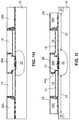
- FIGS. 4A-4Dare cross sectional views illustrating steps in another alternate embodiment for forming a pair of memory cells of the present invention.
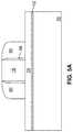
- FIGS. 5A-5Care cross sectional views illustrating steps in another alternate embodiment for forming a pair of memory cells of the present invention.
- FIG. 6is a cross sectional view of another alternate embodiment for forming a pair of memory cells of the present invention.
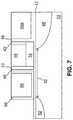
- FIG. 7is a cross sectional view of another alternate embodiment for forming a pair of memory cells of the present invention.
- the present inventionis a method of making pairs of memory cells with a reduced numbers of processing steps (e.g. only two polysilicon deposition steps).
- FIGS. 1A-1Ithere are shown cross-sectional views of the steps in the process to make pairs of memory cells (while only the formation of a single pair of memory cells are shown in the figures, it should be understood that an array of such memory cell pairs are formed concurrently).
- the processbegins by forming a layer of silicon dioxide (oxide) 12 on a substrate 10 of P type single crystalline silicon.
- the oxide layer 12can be 80-100 A thick.
- a layer 14 of polysilicon (or amorphous silicon)is formed on the layer 12 of silicon dioxide.
- Poly layer 14can be 200-300 A thick.
- Oxide layer 16can be 20-50 A thick, and nitride layer 18 can be about 500 A thick.
- Photoresist material(not shown) is coated on the structure, and a masking step is performed exposing selected portions of the photoresist material.
- the photoresistis developed such that portions of the photoresist are removed.
- the structureis etched. Specifically, nitride and oxide layers 18 and 16 are anisotropically etched (using poly layer 14 as an etch stop), leaving pairs of nitride blocks 18 as shown in FIG. 1B (after the photoresist is removed).
- the space between nitride blocks 18is termed herein the “inner region,” and the spaces outside of the pair of nitride blocks are termed herein the “outer regions.”
- Photoresist materialis again coated on the structure, and is patterned using masking and develop steps, to cover the inner region. An anisotropic poly etch is then used to remove those portions of poly layer 14 in the outer regions, as shown in FIG. 1C (after the photoresist is removed).
- Oxide spacers 20are then formed on the sides of the structure. Formation of spacers is well known in the art, and involves the deposition of a material over the contour of a structure, followed by an anisotropic etch process, whereby the material is removed from horizontal surfaces of the structure, while the material remains largely intact on vertically oriented surfaces of the structure (with a rounded upper surface). The resultant structure is shown in FIG. 1D . A poly etch is then used to remove the exposed portion of poly layer 14 in the inner region. An implant process (e.g. implantation and anneal) is then performed to form source region 22 in the substrate in the inner region. The resulting structure is shown in FIG. 1E .
- Photoresistis formed on the structure and removed from the inner region, and an oxide etch is used to remove the oxide spacers 20 in the inner region and the oxide layer 12 over the source region.
- a tunnel oxide layer 24is then formed over the structure (e.g. by high temperature oxide HTO), including the exposed portions of poly layer 14 in the inner region, as shown in FIG. 1F .
- a thick layer 26 of polysiliconis formed over the structure (see FIG. 1G ), followed by a poly etch (e.g. CMP using nitride 18 as an etch stop), leaving a poly block 26 a in the inner region and poly blocks 26 b in the outer regions, as shown in FIG. 1H .
- An optional poly etchcould be used to reduce the height of poly blocks 26 a and 26 b (i.e. below the tops of nitride blocks 18 ).
- Photoresistis formed on the structure and patterned to leave portions of poly blocks 26 b exposed, followed by a poly etch to remove exposed portions of poly blocks 26 (i.e. to define the outside edges of poly blocks 26 b ).
- An implantis then performed to form drain regions 30 in the substrate adjacent the outside edges of poly blocks 26 b .
- Salicide 28is then formed on the exposed upper surfaces of poly blocks 26 a and 26 b (for improved conductivity).
- the final structureis shown in FIG. 1I , and includes a pair of memory cells.
- Each memory cellincludes a source region 22 , a drain region 30 , a channel region 32 in the substrate between the source and drain regions, a floating gate 14 disposed over and insulated from a first portion of the channel region 32 , a word line gate 26 b disposed over and insulated from a second portion of the channel region 32 , and an erase gate 26 a disposed over and insulated from the source region 22 .
- the erase gate 26 ahas a first portion that is laterally adjacent to the floating gate 14 and a second portion that extends up and over a portion of the floating gate 14 .
- the above described manufacturing methodhas several advantages. First, only two poly depositions are used to form all three gates (floating 14 , erase 26 a and word line 26 b ).
- the floating gate 14has a sharp tip or edge 14 a facing a notch 27 in the erase gate 26 a for improved erase efficiency.
- the floating gate 14is relatively thin, while the nitride block 18 above the floating gate 14 is relatively thick and acts as a reliable hard mask and serves as a poly CMP stop layer.
- FIGS. 2-7there are shown cross-sectional views of alternate embodiments of the process to make pairs of memory cells (while only the formation of one memory cell is shown in these figures, it should be understood that a mirror memory cell is concurrently formed on the other side of the source region as part of a pair of memory cells, and that an array of such memory cell pairs are formed concurrently).
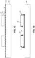
- FIG. 2illustrates an alternate embodiment of the process of FIGS. 1A-1I , wherein the spacer 42 formed over floating gate 14 in the inner region is left remaining before the formation of erase gate 50 a (i.e., no inner region oxide etch), to simplify the fabrication process.
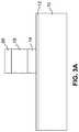
- FIGS. 3A-3Dillustrate yet another alternate embodiment of the process of FIGS. 1A-1I , wherein the process begins with the same processing steps described above and illustrated in FIG. 1A .
- a poly etchis used to remove the poly layer 14 in both the inner and outer regions as shown in FIG. 3A .
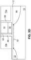
- an additional oxide layer 60is formed on nitride blocks 18 .
- Insulation spacers 62e.g. composite, formed of both oxide and nitride, or just oxide are formed along the sides of nitride block 18 and poly layer 14 , as shown in FIG. 3B .
- Photoresist 64is formed on the structure, and removed from the inner region.
- the exposed ON or oxide spacer 62is removed by nitride/oxide etch.
- An implant processis then used to form source region 66 , as shown in FIG. 3C .
- an oxide layer 68is formed over the structure.
- a poly deposition, CMP and poly etchare then performed to form the erase gate 70 a and word line gate 70 b .
- An implantis then used to form drain 72 .
- the final structureis shown in FIG. 3D . With this embodiment, the spacing between the erase gate 70 a and the floating gate 14 and nitride block 18 is dictated solely by oxide layer 68 .
- FIGS. 4A-4Dillustrate yet another alternate embodiment of the process of FIGS. 1A-1I , wherein the process begins with the same processing steps described above and illustrated in FIG. 1A .
- Spacers 74 of insulation materiale.g. oxide
- Photo resist 76is formed on the structure, and selectively removed from the outer regions.
- a poly etchis used to remove the exposed portions of poly layer 14 .
- a WLVT implantationis used to implant the substrate in the outer regions, as illustrated in FIG. 4A .
- photoresist 78is formed on the structure, and selectively removed from the inner region.
- An oxide wet etchis performed to thin the exposed spacers 74 in the inner region (to independently control the eventual overlap of the erase gate and the floating gate).
- a poly etchis then performed to remove the exposed portions of poly layer 14 in the inner region.
- An implant processis then performed to form source region 80 , as shown in FIG. 4B .
- an oxide etchis performed to remove spacers 74 and exposed portions of oxide layer 12 .
- a thermal oxidation processis used to form oxide layer 82 on the exposed surfaces of poly layer 14 and substrate 10 , as illustrated in FIG. 4C .
- a poly deposition and etchare used to form erase gate 84 a and word line gate 84 b , and an implant is used to form drain region 86 , as illustrated in FIG.
- Both the erase gate 84 a and word line gate 84 bhave a first portion laterally adjacent to the floating gate and a second portion extending up and over the floating gate, for enhanced erase efficiency and capacitive coupling.
- the amount of floating gate overlap by the erase gate relative to the word line gateis independently controlled and dictated by the oxide spacer thinning step.
- FIGS. 5A-5Cillustrate yet another alternate embodiment of the process of FIGS. 1A-1I , wherein the process begins with the same processing steps described above and illustrated in FIG. 1A .
- the erase gatereplaces nitride block 18 instead of being formed next to it.
- spacers 88 (optional) and 90 of insulation materiale.g. oxide-nitride for spacers 88 which is optional, and oxide for spacers 90
- a poly etchis used to remove those portions of poly layer 14 not protected by nitride block 18 and spacers 88 and 90 .
- Spacers 92 of insulation materiale.g.
- oxideare then formed on the sides of the structure, including the exposed ends of poly layer, as illustrated in FIG. 5B .
- a nitride etchis used to remove nitride block 18 leaving a trench behind and exposing a portion of the poly layer 14 at the bottom of the trench.
- a poly etchis used to remove the exposed portion of poly layer 14 .
- An implant processis used to form source region 93 . Spacers 88 are removed or thinned, or spacer 90 is thinned without optional spacer 88 , and oxide 94 is formed along the sidewalls of the trench left behind by the removal of nitride block 18 .
- a poly deposition and etchare performed to form erase gate 96 a and word line gates 96 b .
- An implant processis then used to form drain regions 98 . The resulting structure is shown in FIG. 5C .
- FIG. 6illustrates an alternate embodiment of the process of FIGS. 5A-5C , wherein before spacers 90 are formed, a poly slope etch is performed so that the upper surface of poly layer 14 slopes downwardly as it extends away from nitride block 18 . This results in each floating gate having an upwardly sloping surface terminating in a sharper edge that faces the notch of the erase gate.
- FIG. 7illustrates another alternate embodiment of the processes of FIGS. 1-6 , wherein the poly block that forms the word line gate is removed by poly etch, and replaced with an insulation layer of a high K material (i.e. having a dielectric constant K greater than that of oxide, such as HfO2, ZrO2, TiO2, etc.), and a block of metal material.
- a high K materiali.e. having a dielectric constant K greater than that of oxide, such as HfO2, ZrO2, TiO2, etc.
- poly block 50 bis removed by poly etch, and replaced with an insulation layer 56 of a high K material and a block 58 of metal material, as shown in FIG. 7 .
- the word line gate 58 formed of metalgreater gate conductivity can be achieved.
- poly block 26 b in FIG. 1Ipoly block 70 b in FIG. 3D
- poly block 84 b in FIG. 4Dpoly block 96 b in FIGS. 5C and 6 .
- nitride blocks 18could instead be made of oxide or composite layers with oxide-nitride-oxide, or oxide-nitride.
- the insulator under the word line gates 26 b , 50 b , 70 b , 84 b , and 96 bcan be silicon oxide, or nitrogen treated oxide with NO, N2O anneal or DPN (decoupled plasma nitridation), and is not limited to these examples. Further, as is apparent from the claims and specification, not all method steps need be performed in the exact order illustrated or claimed, but rather in any order that allows the proper formation of the memory cell of the present invention. Lastly, single layers of material could be formed as multiple layers of such or similar materials, and vice versa.
- the term “adjacent”includes “directly adjacent” (no intermediate materials, elements or space disposed therebetween) and “indirectly adjacent” (intermediate materials, elements or space disposed there between), “mounted to” includes “directly mounted to” (no intermediate materials, elements or space disposed there between) and “indirectly mounted to” (intermediate materials, elements or spaced disposed there between), and “electrically coupled” includes “directly electrically coupled to” (no intermediate materials or elements there between that electrically connect the elements together) and “indirectly electrically coupled to” (intermediate materials or elements there between that electrically connect the elements together).
- forming an element “over a substrate”can include forming the element directly on the substrate with no intermediate materials/elements therebetween, as well as forming the element indirectly on the substrate with one or more intermediate materials/elements therebetween.
Landscapes
- Engineering & Computer Science (AREA)
- Power Engineering (AREA)
- Physics & Mathematics (AREA)
- Condensed Matter Physics & Semiconductors (AREA)
- General Physics & Mathematics (AREA)
- Manufacturing & Machinery (AREA)
- Computer Hardware Design (AREA)
- Microelectronics & Electronic Packaging (AREA)
- Non-Volatile Memory (AREA)
- Semiconductor Memories (AREA)
Abstract
Description
- This application is a divisional of Ser. No. 16/245,069, filed Jan. 10, 2019, which is a divisional of Ser. No. 15/474,879, filed Mar. 30, 2017, which claims the benefit of Chinese Patent Application No. 201610247666.6 filed on Apr. 20, 2016, which are incorporated herein by reference.
- The present invention relates to a non-volatile flash memory cell which has a word line (WL) gate, a floating gate, and an erase gate.
- Split gate non-volatile flash memory cells having a word line (WL) gate, a floating gate, and an erase gate are well known in the art. See for example U.S. Pat. No. 7,315,056, which is incorporated herein by reference in its entirety.
- As non-volatile memory cells have reduced in size, it becomes more challenging to fabricate such memory cells in terms of self-aligned elements, and reduced numbers of processing steps (e.g. masking steps, poly deposition steps, etc.). Accordingly, it is one of the objectives of the present invention to simplify the fabrication process as the memory cells continue to shrink in size.
- A simplified method of forming a pair of non-volatile memory cells includes forming a first insulation layer on a semiconductor substrate, forming a first polysilicon layer on the first insulation layer in a first polysilicon deposition process, forming a pair of spaced apart insulation blocks on the first polysilicon layer, each of the insulation blocks having first sides facing toward each other and second sides facing away from each other, forming insulation spacers adjacent the first and second sides, reducing a width of the insulation spacers adjacent the first sides, removing portions of the first polysilicon layer while maintaining a pair of polysilicon blocks of the first polysilicon layer each disposed under one of the pair of insulation blocks and the insulation spacers adjacent the first and second sides of the one insulation block, forming a source region in the substrate and between the pair of insulation blocks, removing the insulation spacers to expose end portions of each of the pair of polysilicon blocks of the first polysilicon layer, forming a layer of insulation material that at least extends along the exposed end portions of each of the pair of polysilicon blocks of the first polysilicon layer, forming a second polysilicon layer over the substrate and the pair of insulation blocks in a second polysilicon deposition process, removing portions of the second polysilicon layer while maintaining a first polysilicon block, a second polysilicon block and a third polysilicon block of the second polysilicon layer (wherein the first polysilicon block is disposed between the pair of insulation blocks and over the source region, the second polysilicon block is disposed adjacent the second side of one of the insulation blocks, and the third polysilicon block is disposed adjacent the second side of another one of the insulation blocks), forming a first drain region in the substrate and adjacent the second polysilicon block, and forming a second drain region in the substrate and adjacent the third polysilicon block.
- A simplified method of forming a pair of non-volatile memory cells includes forming a first insulation layer on a semiconductor substrate, forming a first polysilicon layer on the first insulation layer in a first polysilicon deposition process, forming an insulation block on the first polysilicon layer having opposing first and second sides, forming a first insulation spacer on the first polysilicon layer and adjacent the first side and a second insulation spacer on the first polysilicon layer and adjacent the second side, removing portions of the first polysilicon layer while maintaining a polysilicon block of the first polysilicon layer disposed under the insulation block and first and second insulation spacers, removing the insulation block, removing a portion of the first polysilicon layer disposed between the first and second insulation spacers to form a first polysilicon block of the first polysilicon layer disposed under the first insulation spacer and a second polysilicon block of the first polysilicon layer disposed under the second insulation spacer, forming a source region in the substrate and between the first and second insulation spacers, forming insulation material that at least extends along an end portion of each of the first and second polysilicon blocks of the first polysilicon layer, forming a second polysilicon layer over the substrate and the pair of insulation spacers in a second polysilicon deposition process, removing portions of the second polysilicon layer while maintaining a third polysilicon block, a fourth polysilicon block and a fifth polysilicon block of the second polysilicon layer (wherein the third polysilicon block is disposed between the pair of insulation spacers and over the source region, the fourth polysilicon block is disposed adjacent the first insulation spacer, and the fifth polysilicon block is disposed adjacent the second insulation spacer), forming a first drain region in the substrate and adjacent the fourth polysilicon block, and forming a second drain region in the substrate and adjacent the fifth polysilicon block.
- Other objects and features of the present invention will become apparent by a review of the specification, claims and appended figures.
FIGS. 1A-1I are cross sectional views illustrating steps in forming a pair of memory cells of the present invention.FIG. 2 is a cross sectional view of another alternate embodiment for forming a pair of memory cells of the present invention.FIGS. 3A-3D are cross sectional views illustrating steps in another alternate embodiment for forming a pair of memory cells of the present invention.FIGS. 4A-4D are cross sectional views illustrating steps in another alternate embodiment for forming a pair of memory cells of the present invention.FIGS. 5A-5C are cross sectional views illustrating steps in another alternate embodiment for forming a pair of memory cells of the present invention.FIG. 6 is a cross sectional view of another alternate embodiment for forming a pair of memory cells of the present invention.FIG. 7 is a cross sectional view of another alternate embodiment for forming a pair of memory cells of the present invention.- The present invention is a method of making pairs of memory cells with a reduced numbers of processing steps (e.g. only two polysilicon deposition steps). Referring to
FIGS. 1A-1I , there are shown cross-sectional views of the steps in the process to make pairs of memory cells (while only the formation of a single pair of memory cells are shown in the figures, it should be understood that an array of such memory cell pairs are formed concurrently). The process begins by forming a layer of silicon dioxide (oxide)12 on asubstrate 10 of P type single crystalline silicon. Theoxide layer 12 can be 80-100 A thick. Thereafter alayer 14 of polysilicon (or amorphous silicon) is formed on thelayer 12 of silicon dioxide.Poly layer 14 can be 200-300 A thick. Another insulating layer16 (e.g. oxide) is formed onpoly layer 14, and yet another insulating layer18 (e.g. silicon nitride (nitride)) is formed onoxide layer 16, as shown inFIG. 1A .Oxide layer 16 can be 20-50 A thick, andnitride layer 18 can be about 500 A thick. - Photoresist material (not shown) is coated on the structure, and a masking step is performed exposing selected portions of the photoresist material. The photoresist is developed such that portions of the photoresist are removed. Using the remaining photoresist as a mask, the structure is etched. Specifically, nitride and
oxide layers poly layer 14 as an etch stop), leaving pairs ofnitride blocks 18 as shown inFIG. 1B (after the photoresist is removed). The space betweennitride blocks 18 is termed herein the “inner region,” and the spaces outside of the pair of nitride blocks are termed herein the “outer regions.” Photoresist material is again coated on the structure, and is patterned using masking and develop steps, to cover the inner region. An anisotropic poly etch is then used to remove those portions ofpoly layer 14 in the outer regions, as shown inFIG. 1C (after the photoresist is removed). Oxide spacers 20 are then formed on the sides of the structure. Formation of spacers is well known in the art, and involves the deposition of a material over the contour of a structure, followed by an anisotropic etch process, whereby the material is removed from horizontal surfaces of the structure, while the material remains largely intact on vertically oriented surfaces of the structure (with a rounded upper surface). The resultant structure is shown inFIG. 1D . A poly etch is then used to remove the exposed portion ofpoly layer 14 in the inner region. An implant process (e.g. implantation and anneal) is then performed to formsource region 22 in the substrate in the inner region. The resulting structure is shown inFIG. 1E .- Photoresist is formed on the structure and removed from the inner region, and an oxide etch is used to remove the
oxide spacers 20 in the inner region and theoxide layer 12 over the source region. After photoresist removal, atunnel oxide layer 24 is then formed over the structure (e.g. by high temperature oxide HTO), including the exposed portions ofpoly layer 14 in the inner region, as shown inFIG. 1F . Athick layer 26 of polysilicon is formed over the structure (seeFIG. 1G ), followed by a poly etch (e.g.CMP using nitride 18 as an etch stop), leaving apoly block 26ain the inner region andpoly blocks 26bin the outer regions, as shown inFIG. 1H . An optional poly etch could be used to reduce the height ofpoly blocks - Photoresist is formed on the structure and patterned to leave portions of
poly blocks 26bexposed, followed by a poly etch to remove exposed portions of poly blocks26 (i.e. to define the outside edges ofpoly blocks 26b). An implant is then performed to formdrain regions 30 in the substrate adjacent the outside edges ofpoly blocks 26b.Salicide 28 is then formed on the exposed upper surfaces of poly blocks26aand26b(for improved conductivity). The final structure is shown inFIG. 1I , and includes a pair of memory cells. Each memory cell includes asource region 22, adrain region 30, achannel region 32 in the substrate between the source and drain regions, a floatinggate 14 disposed over and insulated from a first portion of thechannel region 32, aword line gate 26bdisposed over and insulated from a second portion of thechannel region 32, and an erasegate 26adisposed over and insulated from thesource region 22. The erasegate 26ahas a first portion that is laterally adjacent to the floatinggate 14 and a second portion that extends up and over a portion of the floatinggate 14. - The above described manufacturing method has several advantages. First, only two poly depositions are used to form all three gates (floating14, erase26aand
word line 26b). The floatinggate 14 has a sharp tip or edge14afacing anotch 27 in the erasegate 26afor improved erase efficiency. The floatinggate 14 is relatively thin, while thenitride block 18 above the floatinggate 14 is relatively thick and acts as a reliable hard mask and serves as a poly CMP stop layer. - Referring to
FIGS. 2-7 , there are shown cross-sectional views of alternate embodiments of the process to make pairs of memory cells (while only the formation of one memory cell is shown in these figures, it should be understood that a mirror memory cell is concurrently formed on the other side of the source region as part of a pair of memory cells, and that an array of such memory cell pairs are formed concurrently). FIG. 2 illustrates an alternate embodiment of the process ofFIGS. 1A-1I , wherein thespacer 42 formed over floatinggate 14 in the inner region is left remaining before the formation of erasegate 50a(i.e., no inner region oxide etch), to simplify the fabrication process.FIGS. 3A-3D illustrate yet another alternate embodiment of the process ofFIGS. 1A-1I , wherein the process begins with the same processing steps described above and illustrated inFIG. 1A . However, unlike the poly etch that only removes the exposed portions ofpoly layer 14 in the outer regions as shown inFIG. 1C , a poly etch is used to remove thepoly layer 14 in both the inner and outer regions as shown inFIG. 3A . Preferably, anadditional oxide layer 60 is formed on nitride blocks18. Insulation spacers62 (e.g. composite, formed of both oxide and nitride, or just oxide) are formed along the sides ofnitride block 18 andpoly layer 14, as shown inFIG. 3B .Photoresist 64 is formed on the structure, and removed from the inner region. The exposed ON oroxide spacer 62 is removed by nitride/oxide etch. An implant process is then used to formsource region 66, as shown inFIG. 3C . After photoresist removal, anoxide layer 68 is formed over the structure. A poly deposition, CMP and poly etch are then performed to form the erasegate 70aandword line gate 70b. An implant is then used to formdrain 72. The final structure is shown inFIG. 3D . With this embodiment, the spacing between the erasegate 70aand the floatinggate 14 andnitride block 18 is dictated solely byoxide layer 68.FIGS. 4A-4D illustrate yet another alternate embodiment of the process ofFIGS. 1A-1I , wherein the process begins with the same processing steps described above and illustrated inFIG. 1A .Spacers 74 of insulation material (e.g. oxide) are formed on both sides ofnitride block 18. Photo resist76 is formed on the structure, and selectively removed from the outer regions. A poly etch is used to remove the exposed portions ofpoly layer 14. A WLVT implantation is used to implant the substrate in the outer regions, as illustrated inFIG. 4A . After photoresist removal,photoresist 78 is formed on the structure, and selectively removed from the inner region. An oxide wet etch is performed to thin the exposedspacers 74 in the inner region (to independently control the eventual overlap of the erase gate and the floating gate). A poly etch is then performed to remove the exposed portions ofpoly layer 14 in the inner region. An implant process is then performed to formsource region 80, as shown inFIG. 4B . After photoresist removal, an oxide etch is performed to removespacers 74 and exposed portions ofoxide layer 12. A thermal oxidation process is used to formoxide layer 82 on the exposed surfaces ofpoly layer 14 andsubstrate 10, as illustrated inFIG. 4C . A poly deposition and etch are used to form erasegate 84aandword line gate 84b, and an implant is used to formdrain region 86, as illustrated inFIG. 4D . Both the erasegate 84aandword line gate 84bhave a first portion laterally adjacent to the floating gate and a second portion extending up and over the floating gate, for enhanced erase efficiency and capacitive coupling. The amount of floating gate overlap by the erase gate relative to the word line gate is independently controlled and dictated by the oxide spacer thinning step.FIGS. 5A-5C illustrate yet another alternate embodiment of the process ofFIGS. 1A-1I , wherein the process begins with the same processing steps described above and illustrated inFIG. 1A . However, in this embodiment, the erase gate replacesnitride block 18 instead of being formed next to it. Specifically, spacers88 (optional) and90 of insulation material (e.g. oxide-nitride forspacers 88 which is optional, and oxide for spacers90) are formed on both sides ofnitride block 18, as illustrated inFIG. 5A . A poly etch is used to remove those portions ofpoly layer 14 not protected bynitride block 18 andspacers Spacers 92 of insulation material (e.g. oxide) are then formed on the sides of the structure, including the exposed ends of poly layer, as illustrated inFIG. 5B . A nitride etch is used to removenitride block 18 leaving a trench behind and exposing a portion of thepoly layer 14 at the bottom of the trench. A poly etch is used to remove the exposed portion ofpoly layer 14. An implant process is used to formsource region 93.Spacers 88 are removed or thinned, orspacer 90 is thinned withoutoptional spacer 88, andoxide 94 is formed along the sidewalls of the trench left behind by the removal ofnitride block 18. A poly deposition and etch are performed to form erasegate 96aandword line gates 96b. An implant process is then used to formdrain regions 98. The resulting structure is shown inFIG. 5C .FIG. 6 illustrates an alternate embodiment of the process ofFIGS. 5A-5C , wherein before spacers90 are formed, a poly slope etch is performed so that the upper surface ofpoly layer 14 slopes downwardly as it extends away fromnitride block 18. This results in each floating gate having an upwardly sloping surface terminating in a sharper edge that faces the notch of the erase gate.FIG. 7 illustrates another alternate embodiment of the processes ofFIGS. 1-6 , wherein the poly block that forms the word line gate is removed by poly etch, and replaced with an insulation layer of a high K material (i.e. having a dielectric constant K greater than that of oxide, such as HfO2, ZrO2, TiO2, etc.), and a block of metal material. For example, with respect to the embodiment ofFIG. 2 ,poly block 50bis removed by poly etch, and replaced with aninsulation layer 56 of a high K material and ablock 58 of metal material, as shown inFIG. 7 . By having theword line gate 58 formed of metal, greater gate conductivity can be achieved. The same can be done forpoly block 26binFIG. 1I ,poly block 70binFIG. 3D ,poly block 84binFIG. 4D , andpoly block 96binFIGS. 5C and 6 .- It is to be understood that the present invention is not limited to the embodiment(s) described above and illustrated herein, but encompasses any and all variations falling within the scope of the appended claims. For example, references to the present invention herein are not intended to limit the scope of any claim or claim term, but instead merely make reference to one or more features that may be covered by one or more of the claims. Materials, processes and numerical examples described above are exemplary only, and should not be deemed to limit the claims. For example, nitride blocks18 could instead be made of oxide or composite layers with oxide-nitride-oxide, or oxide-nitride. The insulator under the
word line gates - It should be noted that, as used herein, the terms “over” and “on” both inclusively include “directly on” (no intermediate materials, elements or space disposed therebetween) and “indirectly on” (intermediate materials, elements or space disposed therebetween). Likewise, the term “adjacent” includes “directly adjacent” (no intermediate materials, elements or space disposed therebetween) and “indirectly adjacent” (intermediate materials, elements or space disposed there between), “mounted to” includes “directly mounted to” (no intermediate materials, elements or space disposed there between) and “indirectly mounted to” (intermediate materials, elements or spaced disposed there between), and “electrically coupled” includes “directly electrically coupled to” (no intermediate materials or elements there between that electrically connect the elements together) and “indirectly electrically coupled to” (intermediate materials or elements there between that electrically connect the elements together). For example, forming an element “over a substrate” can include forming the element directly on the substrate with no intermediate materials/elements therebetween, as well as forming the element indirectly on the substrate with one or more intermediate materials/elements therebetween.
Claims (14)
Priority Applications (2)
| Application Number | Priority Date | Filing Date | Title |
|---|---|---|---|
| US17/021,678US11652162B2 (en) | 2016-04-20 | 2020-09-15 | Method of forming a three-gate non-volatile flash memory cell using two polysilicon deposition steps |
| US18/126,954US20230238453A1 (en) | 2016-04-20 | 2023-03-27 | Method of forming pairs of three-gate non-volatile flash memory cells using two polysilicon deposition steps |
Applications Claiming Priority (5)
| Application Number | Priority Date | Filing Date | Title |
|---|---|---|---|
| CN201610247666.6ACN107305892B (en) | 2016-04-20 | 2016-04-20 | Method of Forming Tri-Gate Non-Volatile Flash Memory Cell Pairs Using Two Polysilicon Deposition Steps |
| CN201610247666.6 | 2016-04-20 | ||
| US15/474,879US10217850B2 (en) | 2016-04-20 | 2017-03-30 | Method of forming pairs of three-gate non-volatile flash memory cells using two polysilicon deposition steps |
| US16/245,069US20190148529A1 (en) | 2016-04-20 | 2019-01-10 | Method Of Forming Pairs Of Three-Gate Non-volatile Flash Memory Cells Using Two Polysilicon Deposition Steps |
| US17/021,678US11652162B2 (en) | 2016-04-20 | 2020-09-15 | Method of forming a three-gate non-volatile flash memory cell using two polysilicon deposition steps |
Related Parent Applications (1)
| Application Number | Title | Priority Date | Filing Date |
|---|---|---|---|
| US16/245,069DivisionUS20190148529A1 (en) | 2016-04-20 | 2019-01-10 | Method Of Forming Pairs Of Three-Gate Non-volatile Flash Memory Cells Using Two Polysilicon Deposition Steps |
Related Child Applications (1)
| Application Number | Title | Priority Date | Filing Date |
|---|---|---|---|
| US18/126,954DivisionUS20230238453A1 (en) | 2016-04-20 | 2023-03-27 | Method of forming pairs of three-gate non-volatile flash memory cells using two polysilicon deposition steps |
Publications (2)
| Publication Number | Publication Date |
|---|---|
| US20200411673A1true US20200411673A1 (en) | 2020-12-31 |
| US11652162B2 US11652162B2 (en) | 2023-05-16 |
Family
ID=60151593
Family Applications (4)
| Application Number | Title | Priority Date | Filing Date |
|---|---|---|---|
| US15/474,879ActiveUS10217850B2 (en) | 2016-04-20 | 2017-03-30 | Method of forming pairs of three-gate non-volatile flash memory cells using two polysilicon deposition steps |
| US16/245,069AbandonedUS20190148529A1 (en) | 2016-04-20 | 2019-01-10 | Method Of Forming Pairs Of Three-Gate Non-volatile Flash Memory Cells Using Two Polysilicon Deposition Steps |
| US17/021,678Active2037-06-02US11652162B2 (en) | 2016-04-20 | 2020-09-15 | Method of forming a three-gate non-volatile flash memory cell using two polysilicon deposition steps |
| US18/126,954AbandonedUS20230238453A1 (en) | 2016-04-20 | 2023-03-27 | Method of forming pairs of three-gate non-volatile flash memory cells using two polysilicon deposition steps |
Family Applications Before (2)
| Application Number | Title | Priority Date | Filing Date |
|---|---|---|---|
| US15/474,879ActiveUS10217850B2 (en) | 2016-04-20 | 2017-03-30 | Method of forming pairs of three-gate non-volatile flash memory cells using two polysilicon deposition steps |
| US16/245,069AbandonedUS20190148529A1 (en) | 2016-04-20 | 2019-01-10 | Method Of Forming Pairs Of Three-Gate Non-volatile Flash Memory Cells Using Two Polysilicon Deposition Steps |
Family Applications After (1)
| Application Number | Title | Priority Date | Filing Date |
|---|---|---|---|
| US18/126,954AbandonedUS20230238453A1 (en) | 2016-04-20 | 2023-03-27 | Method of forming pairs of three-gate non-volatile flash memory cells using two polysilicon deposition steps |
Country Status (6)
| Country | Link |
|---|---|
| US (4) | US10217850B2 (en) |
| EP (1) | EP3446336A4 (en) |
| JP (1) | JP6716716B2 (en) |
| KR (3) | KR102125469B1 (en) |
| CN (1) | CN107305892B (en) |
| TW (1) | TWI641114B (en) |
Cited By (1)
| Publication number | Priority date | Publication date | Assignee | Title |
|---|---|---|---|---|
| US11652162B2 (en)* | 2016-04-20 | 2023-05-16 | Silicon Storage Technology, Inc. | Method of forming a three-gate non-volatile flash memory cell using two polysilicon deposition steps |
Families Citing this family (10)
| Publication number | Priority date | Publication date | Assignee | Title |
|---|---|---|---|---|
| CN108091659B (en)* | 2017-11-30 | 2021-01-01 | 上海华虹宏力半导体制造有限公司 | Split-gate flash memory unit and preparation method thereof |
| US10347728B1 (en)* | 2018-01-02 | 2019-07-09 | Microchip Technology Incorporated | Memory cell with asymmetric word line and erase gate for decoupled program erase performance |
| CN110071109B (en)* | 2018-01-24 | 2022-07-29 | 世界先进积体电路股份有限公司 | Forming method of separated grid flash memory element |
| CN112185815B (en)* | 2019-07-04 | 2024-07-23 | 硅存储技术公司 | Method for forming split gate flash memory cell |
| US11114451B1 (en) | 2020-02-27 | 2021-09-07 | Silicon Storage Technology, Inc. | Method of forming a device with FinFET split gate non-volatile memory cells and FinFET logic devices |
| US11362100B2 (en) | 2020-03-24 | 2022-06-14 | Silicon Storage Technology, Inc. | FinFET split gate non-volatile memory cells with enhanced floating gate to floating gate capacitive coupling |
| CN114335186B (en)* | 2020-09-30 | 2025-02-07 | 硅存储技术股份有限公司 | Split gate non-volatile memory cell with erase gate disposed above word line gate and method of making the same |
| CN113206010B (en)* | 2021-04-30 | 2023-10-24 | 广东省大湾区集成电路与系统应用研究院 | Semiconductor device and method for manufacturing the same |
| CN113394103B (en) | 2021-05-25 | 2024-08-06 | 上海华力集成电路制造有限公司 | A method for manufacturing a triple-gate structure semi-floating gate transistor |
| CN116322046A (en)* | 2023-02-14 | 2023-06-23 | 芯合半导体有限公司 | Split gate nonvolatile memory device and method of manufacturing the same |
Citations (38)
| Publication number | Priority date | Publication date | Assignee | Title |
|---|---|---|---|---|
| US5070032A (en)* | 1989-03-15 | 1991-12-03 | Sundisk Corporation | Method of making dense flash eeprom semiconductor memory structures |
| US5095344A (en)* | 1988-06-08 | 1992-03-10 | Eliyahou Harari | Highly compact eprom and flash eeprom devices |
| US5101250A (en)* | 1988-06-28 | 1992-03-31 | Mitsubishi Denki Kabushiki Kaisha | Electrically programmable non-volatile memory device and manufacturing method thereof |
| US20020034849A1 (en)* | 2000-09-20 | 2002-03-21 | Wang Chih Hsin | Self aligned method of forming a semiconductor memory array of floating gate memory cells with low resistance source regions and high source coupling, and a memory array made thereby |
| US20020034846A1 (en)* | 2000-09-20 | 2002-03-21 | Wang Chih Hsin | Self aligned method of forming a semiconductor memory array of floating gate memory cells with control gate spacers, and a memory array made thereby |
| US20020110983A1 (en)* | 2001-02-09 | 2002-08-15 | Chih-Cheng Liu | Method of fabricating a split-gate flash memory cell |
| US6486509B1 (en)* | 1997-09-09 | 2002-11-26 | Imec Vzw | Non-volatile memory cell |
| US6541324B1 (en)* | 2001-11-02 | 2003-04-01 | Silicon Storage Technology, Inc. | Method of forming a semiconductor array of floating gate memory cells having strap regions and a peripheral logic device region |
| US6563167B2 (en)* | 2001-01-05 | 2003-05-13 | Silicon Storage Technology, Inc. | Semiconductor memory array of floating gate memory cells with floating gates having multiple sharp edges |
| US20050199956A1 (en)* | 2004-03-10 | 2005-09-15 | Yi Ding | Fabrication of conductive lines interconnecting conductive gates in nonvolatile memories, and non-volatile memory structures |
| US20050269622A1 (en)* | 2004-06-07 | 2005-12-08 | Pavel Klinger | Semiconductor memory array of floating gate memory cells with program/erase and select gates, and methods of making and operating same |
| US20060113584A1 (en)* | 2004-11-08 | 2006-06-01 | Sanyo Electric Co., Ltd. | Manufacturing method of a semiconductor device |
| US20080217675A1 (en)* | 2007-03-07 | 2008-09-11 | Shih-Chang Liu | Novel profile of flash memory cells |
| US20090207662A1 (en)* | 2008-02-20 | 2009-08-20 | Taiwan Semiconductor Manufacturing Company, Ltd. | Multi-Transistor Non-Volatile Memory Element |
| US20090294832A1 (en)* | 2008-06-03 | 2009-12-03 | Infineon Technologies Ag | Semiconductor Device |
| US20100308392A1 (en)* | 2009-06-05 | 2010-12-09 | Nec Electronics Corporation | Nonvolatile semiconductor storage device |
| US20110049605A1 (en)* | 2009-08-28 | 2011-03-03 | Renesas Electronics Corporation | Split gate nonvolatile semiconductor storage device and method of manufacturing split gate nonvolatile semiconductor storage device |
| US8059473B2 (en)* | 2004-12-30 | 2011-11-15 | Samsung Electronics Co., Ltd. | Non-volatile memory device |
| US8138524B2 (en)* | 2006-11-01 | 2012-03-20 | Silicon Storage Technology, Inc. | Self-aligned method of forming a semiconductor memory array of floating memory cells with source side erase, and a memory array made thereby |
| US20150263040A1 (en)* | 2014-03-17 | 2015-09-17 | Silicon Storage Technology, Inc. | Embedded Memory Device With Silicon-On-Insulator Substrate, And Method Of Making Same |
| US9245638B2 (en)* | 2011-05-13 | 2016-01-26 | Silicon Storage Technology, Inc. | Method of operating a split gate flash memory cell with coupling gate |
| US20160064394A1 (en)* | 2014-08-29 | 2016-03-03 | Taiwan Semiconductor Manufacturing Co., Ltd. | Integrated Circuit for High-Voltage Device Protection |
| US20160141407A1 (en)* | 2014-11-14 | 2016-05-19 | Lapis Semiconductor Co., Ltd. | Semiconductor device and method of manufacturing semiconductor device |
| US20160204274A1 (en)* | 2015-01-13 | 2016-07-14 | Xinnova Technology Limited | Non-volatile memory unit and method for manufacturing the same |
| US20170062448A1 (en)* | 2015-08-28 | 2017-03-02 | Renesas Electronics Corporation | Semiconductor device and method of manufacturing semiconductor device |
| US20170125603A1 (en)* | 2015-11-03 | 2017-05-04 | Silicon Storage Technology, Inc. | Integration Of Metal Floating Gate In Non-Volatile Memory |
| US9673208B2 (en)* | 2015-10-12 | 2017-06-06 | Silicon Storage Technology, Inc. | Method of forming memory array and logic devices |
| US9793279B2 (en)* | 2015-07-10 | 2017-10-17 | Silicon Storage Technology, Inc. | Split gate non-volatile memory cell having a floating gate, word line, erase gate, and method of manufacturing |
| US20170301683A1 (en)* | 2016-04-19 | 2017-10-19 | United Microelectronics Corp. | Semiconductor device with split gate flash memory cell structure and method of manufacturing the same |
| US20170345832A1 (en)* | 2016-05-24 | 2017-11-30 | Taiwan Semiconductor Manufacturing Co., Ltd. | NVM Memory HKMG Integration Technology |
| US10217850B2 (en)* | 2016-04-20 | 2019-02-26 | Silicon Storage Technology, Inc. | Method of forming pairs of three-gate non-volatile flash memory cells using two polysilicon deposition steps |
| US10424589B2 (en)* | 2018-02-13 | 2019-09-24 | Microchip Technology Incorporated | Floating gate spacer for controlling a source region formation in a memory cell |
| US10553596B2 (en)* | 2016-12-12 | 2020-02-04 | Texas Instruments Incorporated | Select gate self-aligned patterning in split-gate flash memory cell |
| US10608090B2 (en)* | 2017-10-04 | 2020-03-31 | Silicon Storage Technology, Inc. | Method of manufacturing a split-gate flash memory cell with erase gate |
| US10644139B2 (en)* | 2016-05-18 | 2020-05-05 | Silicon Storage Technology, Inc. | Method of making split gate non-volatile flash memory cell |
| US10714634B2 (en)* | 2017-12-05 | 2020-07-14 | Silicon Storage Technology, Inc. | Non-volatile split gate memory cells with integrated high K metal control gates and method of making same |
| US10868197B1 (en)* | 2019-05-20 | 2020-12-15 | United Microelectronics Corp. | Structure of memory device and fabrication method thereof |
| US11056495B2 (en)* | 2019-06-13 | 2021-07-06 | United Microelectronics Corp. | Structure of memory device having floating gate with protruding structure |
Family Cites Families (102)
| Publication number | Priority date | Publication date | Assignee | Title |
|---|---|---|---|---|
| US5268319A (en)* | 1988-06-08 | 1993-12-07 | Eliyahou Harari | Highly compact EPROM and flash EEPROM devices |
| US6043530A (en)* | 1998-04-15 | 2000-03-28 | Chang; Ming-Bing | Flash EEPROM device employing polysilicon sidewall spacer as an erase gate |
| US6876031B1 (en)* | 1999-02-23 | 2005-04-05 | Winbond Electronics Corporation | Method and apparatus for split gate source side injection flash memory cell and array with dedicated erase gates |
| JP4222675B2 (en)* | 1999-03-29 | 2009-02-12 | 三洋電機株式会社 | Nonvolatile semiconductor memory device |
| US6338993B1 (en) | 1999-08-18 | 2002-01-15 | Worldwide Semiconductor Manufacturing Corp. | Method to fabricate embedded DRAM with salicide logic cell structure |
| KR100308128B1 (en)* | 1999-08-24 | 2001-11-01 | 김영환 | Non-volatile memory device and method of manufacturing the same |
| TW480676B (en)* | 2001-03-28 | 2002-03-21 | Nanya Technology Corp | Manufacturing method of flash memory cell |
| KR100441682B1 (en)* | 2001-06-14 | 2004-07-27 | 삼성전자주식회사 | Semiconductor device having LDD-type source/drain regions and fabrication method thereof |
| US6403424B1 (en)* | 2001-10-02 | 2002-06-11 | Macronix International Co., Ltd. | Method for forming self-aligned mask read only memory by dual damascene trenches |
| US6747310B2 (en)* | 2002-10-07 | 2004-06-08 | Actrans System Inc. | Flash memory cells with separated self-aligned select and erase gates, and process of fabrication |
| US6962851B2 (en)* | 2003-03-19 | 2005-11-08 | Promos Technologies, Inc. | Nonvolatile memories and methods of fabrication |
| US20040256657A1 (en)* | 2003-06-20 | 2004-12-23 | Chih-Wei Hung | [flash memory cell structure and method of manufacturing and operating the memory cell] |
| KR100518588B1 (en)* | 2003-08-07 | 2005-10-04 | 삼성전자주식회사 | Split gate type non-volatile semiconductor memory device having double-floating gate structure and process for manufacturing the same |
| US6992929B2 (en)* | 2004-03-17 | 2006-01-31 | Actrans System Incorporation, Usa | Self-aligned split-gate NAND flash memory and fabrication process |
| US7046552B2 (en)* | 2004-03-17 | 2006-05-16 | Actrans System Incorporation, Usa | Flash memory with enhanced program and erase coupling and process of fabricating the same |
| US7075830B2 (en)* | 2004-05-21 | 2006-07-11 | United Microelectronics Corp. | Method for programming single-bit storage SONOS type memory |
| TWI235462B (en)* | 2004-07-21 | 2005-07-01 | Powerchip Semiconductor Corp | Nonvolatile memory and manufacturing method thereof |
| JP2006253685A (en)* | 2005-03-07 | 2006-09-21 | Samsung Electronics Co Ltd | Split gate nonvolatile memory device and method of forming the same |
| CN100378961C (en)* | 2005-04-18 | 2008-04-02 | 力晶半导体股份有限公司 | Method for manufacturing non-volatile memory |
| KR100684897B1 (en)* | 2005-04-29 | 2007-02-20 | 삼성전자주식회사 | Split gate type nonvolatile memory and manufacturing method |
| US7242051B2 (en)* | 2005-05-20 | 2007-07-10 | Silicon Storage Technology, Inc. | Split gate NAND flash memory structure and array, method of programming, erasing and reading thereof, and method of manufacturing |
| TWI284415B (en)* | 2005-10-26 | 2007-07-21 | Promos Technologies Inc | Split gate flash memory cell and fabrication method thereof |
| US7655970B2 (en)* | 2006-02-22 | 2010-02-02 | Macronix International Co., Ltd. | Single poly non-volatile memory device with inversion diffusion regions and methods for operating the same |
| US7598561B2 (en)* | 2006-05-05 | 2009-10-06 | Silicon Storage Technolgy, Inc. | NOR flash memory |
| KR100823164B1 (en)* | 2006-11-15 | 2008-04-18 | 삼성전자주식회사 | Nonvolatile Memory Device and Formation Method |
| US7785966B2 (en)* | 2006-12-21 | 2010-08-31 | Taiwan Semiconductor Manufacturing Co., Ltd. | Method for fabricating floating gates structures with reduced and more uniform forward tunneling voltages |
| US20090039410A1 (en)* | 2007-08-06 | 2009-02-12 | Xian Liu | Split Gate Non-Volatile Flash Memory Cell Having A Floating Gate, Control Gate, Select Gate And An Erase Gate With An Overhang Over The Floating Gate, Array And Method Of Manufacturing |
| US20090098721A1 (en)* | 2007-10-16 | 2009-04-16 | Michael-Y Liu | Method of fabricating a flash memory |
| US7800159B2 (en)* | 2007-10-24 | 2010-09-21 | Silicon Storage Technology, Inc. | Array of contactless non-volatile memory cells |
| JP5503843B2 (en)* | 2007-12-27 | 2014-05-28 | ルネサスエレクトロニクス株式会社 | Nonvolatile semiconductor memory device and manufacturing method thereof |
| JP5190986B2 (en)* | 2008-02-08 | 2013-04-24 | ルネサスエレクトロニクス株式会社 | Nonvolatile semiconductor memory device and manufacturing method thereof |
| JP2009188293A (en)* | 2008-02-08 | 2009-08-20 | Nec Electronics Corp | Nonvolatile semiconductor memory device and manufacturing method thereof |
| US7611941B1 (en)* | 2008-06-18 | 2009-11-03 | Infineon Technologies Ag | Method for manufacturing a memory cell arrangement |
| US8445953B2 (en)* | 2009-07-08 | 2013-05-21 | Taiwan Semiconductor Manufacturing Company, Ltd. | Structure for flash memory cells |
| US8334560B2 (en)* | 2009-09-02 | 2012-12-18 | Taiwan Semiconductor Manufacturing Company, Ltd. | Reverse disturb immune asymmetrical sidewall floating gate devices |
| US8563386B2 (en)* | 2010-11-16 | 2013-10-22 | Globalfoundries Singapore Pte. Ltd. | Integrated circuit system with bandgap material and method of manufacture thereof |
| TWI422017B (en)* | 2011-04-18 | 2014-01-01 | Powerchip Technology Corp | Non-volatile memory element and method of manufacturing same |
| US8883592B2 (en)* | 2011-08-05 | 2014-11-11 | Silicon Storage Technology, Inc. | Non-volatile memory cell having a high K dielectric and metal gate |
| CN102956643A (en)* | 2011-08-24 | 2013-03-06 | 硅存储技术公司 | Non-volatile floating gate storage unit manufacturing method and storage unit manufactured by same |
| US8951864B2 (en)* | 2012-02-13 | 2015-02-10 | Taiwan Semiconductor Manufacturing Company, Ltd. | Split-gate device and method of fabricating the same |
| US9330922B2 (en) | 2012-03-07 | 2016-05-03 | Silicon Storage Technology, Inc. | Self-aligned stack gate structure for use in a non-volatile memory array and a method of forming such structure |
| US8878281B2 (en)* | 2012-05-23 | 2014-11-04 | Taiwan Semiconductor Manufacturing Company, Ltd. | Methods and apparatus for non-volatile memory cells |
| US8890230B2 (en)* | 2012-07-15 | 2014-11-18 | United Microelectronics Corp. | Semiconductor device |
| US8785307B2 (en)* | 2012-08-23 | 2014-07-22 | Silicon Storage Technology, Inc. | Method of forming a memory cell by reducing diffusion of dopants under a gate |
| US9018690B2 (en) | 2012-09-28 | 2015-04-28 | Silicon Storage Technology, Inc. | Split-gate memory cell with substrate stressor region, and method of making same |
| US8669607B1 (en)* | 2012-11-01 | 2014-03-11 | Taiwan Semiconductor Manufacturing Company, Ltd. | Methods and apparatus for non-volatile memory cells with increased programming efficiency |
| JP6114534B2 (en)* | 2012-11-07 | 2017-04-12 | ルネサスエレクトロニクス株式会社 | Semiconductor device and manufacturing method of semiconductor device |
| JP6081228B2 (en)* | 2013-02-28 | 2017-02-15 | ルネサスエレクトロニクス株式会社 | Semiconductor device and manufacturing method thereof |
| US9293359B2 (en)* | 2013-03-14 | 2016-03-22 | Silicon Storage Technology, Inc. | Non-volatile memory cells with enhanced channel region effective width, and method of making same |
| KR102008738B1 (en)* | 2013-03-15 | 2019-08-08 | 삼성전자주식회사 | Semiconductor devices and methods of manufacturing the same |
| US9484261B2 (en)* | 2013-07-05 | 2016-11-01 | Silicon Storage Technology, Inc. | Formation of self-aligned source for split-gate non-volatile memory cell |
| US9431256B2 (en)* | 2013-07-11 | 2016-08-30 | United Microelectronics Corp. | Semiconductor device and manufacturing method thereof |
| US9123822B2 (en)* | 2013-08-02 | 2015-09-01 | Silicon Storage Technology, Inc. | Split gate non-volatile flash memory cell having a silicon-metal floating gate and method of making same |
| US9111867B2 (en)* | 2013-08-30 | 2015-08-18 | Freescale Semiconductor, Inc. | Split gate nanocrystal memory integration |
| US9236453B2 (en)* | 2013-09-27 | 2016-01-12 | Ememory Technology Inc. | Nonvolatile memory structure and fabrication method thereof |
| FR3012673B1 (en)* | 2013-10-31 | 2017-04-14 | St Microelectronics Rousset | HOT CARRIER INJECTION PROGRAMMABLE MEMORY AND METHOD OF PROGRAMMING SUCH A MEMORY |
| US9184252B2 (en)* | 2013-11-15 | 2015-11-10 | Taiwan Semiconductor Manufacturing Company, Ltd. | Flash memory embedded with HKMG technology |
| JP2015130438A (en)* | 2014-01-08 | 2015-07-16 | ルネサスエレクトロニクス株式会社 | Semiconductor device and semiconductor device manufacturing method |
| US9202817B2 (en)* | 2014-01-22 | 2015-12-01 | Taiwan Semiconductorr Manufacturing Co., Ltd. | Semiconductor device and method for manufacturing the same |
| US9287282B2 (en)* | 2014-01-28 | 2016-03-15 | Taiwan Semiconductor Manufacturing Company, Ltd. | Method of forming a logic compatible flash memory |
| CN104934427B (en)* | 2014-03-19 | 2018-04-13 | 中芯国际集成电路制造(上海)有限公司 | Flash cell and its manufacture method |
| KR20150121399A (en) | 2014-04-18 | 2015-10-29 | 에스케이하이닉스 주식회사 | Non-volatile memory device having charge trapping layer and method of fabricating the same |
| US9379222B2 (en)* | 2014-05-30 | 2016-06-28 | Freescale Semiconductor, Inc. | Method of making a split gate non-volatile memory (NVM) cell |
| JP6238235B2 (en) | 2014-06-13 | 2017-11-29 | ルネサスエレクトロニクス株式会社 | Semiconductor device |
| US9614048B2 (en)* | 2014-06-17 | 2017-04-04 | Taiwan Semiconductor Manufacturing Co., Ltd. | Split gate flash memory structure and method of making the split gate flash memory structure |
| US9691883B2 (en)* | 2014-06-19 | 2017-06-27 | Taiwan Semiconductor Manufacturing Co., Ltd. | Asymmetric formation approach for a floating gate of a split gate flash memory structure |
| US9252150B1 (en)* | 2014-07-29 | 2016-02-02 | Taiwan Semiconductor Manufacturing Co., Ltd. | High endurance non-volatile memory cell |
| TWI563635B (en) | 2014-09-16 | 2016-12-21 | Winbond Electronics Corp | Non-volatile memory device and method for fabricating thereof |
| KR102170334B1 (en)* | 2014-10-31 | 2020-10-26 | 에스케이하이닉스 주식회사 | Non-volatile memory device having a single-layer gate |
| US10312248B2 (en)* | 2014-11-12 | 2019-06-04 | Silicon Storage Technology, Inc. | Virtual ground non-volatile memory array |
| US9960172B2 (en)* | 2014-11-19 | 2018-05-01 | Globalfoundries Singapore Pte. Ltd. | Reliable non-volatile memory device |
| KR102240022B1 (en)* | 2014-11-26 | 2021-04-15 | 삼성전자주식회사 | Semicondcutor device and manufacturing method for the same |
| CN105655338A (en)* | 2014-12-04 | 2016-06-08 | 联华电子股份有限公司 | Non-volatile memory unit and manufacturing method thereof |
| TWI566381B (en)* | 2014-12-05 | 2017-01-11 | 力晶科技股份有限公司 | Non-volatile memory and method of manufacturing same |
| US9484352B2 (en)* | 2014-12-17 | 2016-11-01 | Taiwan Semiconductor Manufacturing Co., Ltd. | Method for forming a split-gate flash memory cell device with a low power logic device |
| US9673204B2 (en)* | 2014-12-29 | 2017-06-06 | Taiwan Semiconductor Manufacturing Co., Ltd. | Semiconductor device structure and method for forming the same |
| US9276006B1 (en)* | 2015-01-05 | 2016-03-01 | Silicon Storage Technology, Inc. | Split gate non-volatile flash memory cell having metal-enhanced gates and method of making same |
| US9379121B1 (en)* | 2015-01-05 | 2016-06-28 | Silicon Storage Technology, Inc. | Split gate non-volatile flash memory cell having metal gates and method of making same |
| JP6503077B2 (en)* | 2015-01-22 | 2019-04-17 | シリコン ストーリッジ テクノロージー インコーポレイテッドSilicon Storage Technology, Inc. | High density split gate memory cell |
| WO2016118785A1 (en)* | 2015-01-23 | 2016-07-28 | Silicon Storage Technology, Inc. | Method of forming self-aligned split-gate memory cell array with metal gates and logic devices |
| TWI606551B (en)* | 2015-02-16 | 2017-11-21 | Xinnova Tech Ltd | Non-volatile memory device method |
| US9793280B2 (en)* | 2015-03-04 | 2017-10-17 | Silicon Storage Technology, Inc. | Integration of split gate flash memory array and logic devices |
| US9406687B1 (en)* | 2015-03-23 | 2016-08-02 | Globalfoundries Singapore Pte. Ltd. | Integration of memory devices with different voltages |
| US10134475B2 (en)* | 2015-03-31 | 2018-11-20 | Silicon Storage Technology, Inc. | Method and apparatus for inhibiting the programming of unselected bitlines in a flash memory system |
| US9917165B2 (en)* | 2015-05-15 | 2018-03-13 | Taiwan Semiconductor Manufacturing Co., Ltd. | Memory cell structure for improving erase speed |
| US9793281B2 (en) | 2015-07-21 | 2017-10-17 | Silicon Storage Technology, Inc. | Non-volatile split gate memory cells with integrated high K metal gate logic device and metal-free erase gate, and method of making same |
| US9711513B2 (en)* | 2015-08-14 | 2017-07-18 | Globalfoundries Inc. | Semiconductor structure including a nonvolatile memory cell and method for the formation thereof |
| JP2017045755A (en)* | 2015-08-24 | 2017-03-02 | ルネサスエレクトロニクス株式会社 | Semiconductor device and manufacturing method thereof |
| US9634019B1 (en)* | 2015-10-01 | 2017-04-25 | Silicon Storage Technology, Inc. | Non-volatile split gate memory cells with integrated high K metal gate, and method of making same |
| US9754951B2 (en)* | 2015-10-30 | 2017-09-05 | Globalfoundries Inc. | Semiconductor device with a memory device and a high-K metal gate transistor |
| US9548312B1 (en)* | 2015-11-10 | 2017-01-17 | Globalfoundries Inc. | Method including a formation of a control gate of a nonvolatile memory cell and semiconductor structure including a nonvolatile memory cell |
| US9583499B1 (en)* | 2015-11-25 | 2017-02-28 | Globalfoundries Singapore Pte. Ltd. | Devices with embedded non-volatile memory and metal gates and methods for fabricating the same |
| US9825046B2 (en)* | 2016-01-05 | 2017-11-21 | Taiwan Semiconductor Manufacturing Co., Ltd. | Flash memory device having high coupling ratio |
| CN107026171A (en)* | 2016-01-29 | 2017-08-08 | 联华电子股份有限公司 | Flash memory and manufacturing method thereof |
| CN107342288B (en)* | 2016-04-29 | 2020-08-04 | 硅存储技术公司 | Split-gate dual-bit non-volatile memory cell |
| US9922986B2 (en)* | 2016-05-16 | 2018-03-20 | Globalfoundries Inc. | Semiconductor structure including a plurality of pairs of nonvolatile memory cells and an edge cell and method for the formation thereof |
| US9947676B2 (en)* | 2016-07-08 | 2018-04-17 | Taiwan Semiconductor Manufacturing Co., Ltd. | NVM memory HKMG integration technology |
| US10475891B2 (en)* | 2016-10-06 | 2019-11-12 | Globalfoundries Singapore Pte. Ltd. | Reliable non-volatile memory device |
| US10103156B2 (en)* | 2017-02-16 | 2018-10-16 | Globalfoundries Singapore Pte. Ltd. | Strap layout for non-volatile memory device |
| US10546947B2 (en)* | 2017-09-27 | 2020-01-28 | Microchip Technology Incorporated | Memory cell with oxide cap and spacer layer for protecting a floating gate from a source implant |
| US10700077B2 (en)* | 2018-01-02 | 2020-06-30 | Microchip Technology Incorporated | Memory cell with a flat-topped floating gate structure |
| US10861550B1 (en)* | 2019-06-06 | 2020-12-08 | Microchip Technology Incorporated | Flash memory cell adapted for low voltage and/or non-volatile performance |
- 2016
- 2016-04-20CNCN201610247666.6Apatent/CN107305892B/enactiveActive
- 2017
- 2017-03-30USUS15/474,879patent/US10217850B2/enactiveActive
- 2017-03-31EPEP17786312.3Apatent/EP3446336A4/enactivePending
- 2017-03-31KRKR1020187032732Apatent/KR102125469B1/enactiveActive
- 2017-03-31JPJP2018554740Apatent/JP6716716B2/enactiveActive
- 2017-03-31KRKR1020207017319Apatent/KR102221577B1/enactiveActive
- 2017-03-31KRKR1020217005278Apatent/KR102237584B1/enactiveActive
- 2017-04-11TWTW106112013Apatent/TWI641114B/enactive
- 2019
- 2019-01-10USUS16/245,069patent/US20190148529A1/ennot_activeAbandoned
- 2020
- 2020-09-15USUS17/021,678patent/US11652162B2/enactiveActive
- 2023
- 2023-03-27USUS18/126,954patent/US20230238453A1/ennot_activeAbandoned
Patent Citations (41)
| Publication number | Priority date | Publication date | Assignee | Title |
|---|---|---|---|---|
| US5095344A (en)* | 1988-06-08 | 1992-03-10 | Eliyahou Harari | Highly compact eprom and flash eeprom devices |
| US5101250A (en)* | 1988-06-28 | 1992-03-31 | Mitsubishi Denki Kabushiki Kaisha | Electrically programmable non-volatile memory device and manufacturing method thereof |
| US5070032A (en)* | 1989-03-15 | 1991-12-03 | Sundisk Corporation | Method of making dense flash eeprom semiconductor memory structures |
| US6486509B1 (en)* | 1997-09-09 | 2002-11-26 | Imec Vzw | Non-volatile memory cell |
| US6855980B2 (en)* | 2000-09-20 | 2005-02-15 | Silicon Storage Technology, Inc. | Semiconductor memory array of floating gate memory cells with low resistance source regions and high source coupling |
| US20020034849A1 (en)* | 2000-09-20 | 2002-03-21 | Wang Chih Hsin | Self aligned method of forming a semiconductor memory array of floating gate memory cells with low resistance source regions and high source coupling, and a memory array made thereby |
| US20020034846A1 (en)* | 2000-09-20 | 2002-03-21 | Wang Chih Hsin | Self aligned method of forming a semiconductor memory array of floating gate memory cells with control gate spacers, and a memory array made thereby |
| US6563167B2 (en)* | 2001-01-05 | 2003-05-13 | Silicon Storage Technology, Inc. | Semiconductor memory array of floating gate memory cells with floating gates having multiple sharp edges |
| US20020110983A1 (en)* | 2001-02-09 | 2002-08-15 | Chih-Cheng Liu | Method of fabricating a split-gate flash memory cell |
| US6541324B1 (en)* | 2001-11-02 | 2003-04-01 | Silicon Storage Technology, Inc. | Method of forming a semiconductor array of floating gate memory cells having strap regions and a peripheral logic device region |
| US20050199956A1 (en)* | 2004-03-10 | 2005-09-15 | Yi Ding | Fabrication of conductive lines interconnecting conductive gates in nonvolatile memories, and non-volatile memory structures |
| US20050269622A1 (en)* | 2004-06-07 | 2005-12-08 | Pavel Klinger | Semiconductor memory array of floating gate memory cells with program/erase and select gates, and methods of making and operating same |
| US20060113584A1 (en)* | 2004-11-08 | 2006-06-01 | Sanyo Electric Co., Ltd. | Manufacturing method of a semiconductor device |
| US8059473B2 (en)* | 2004-12-30 | 2011-11-15 | Samsung Electronics Co., Ltd. | Non-volatile memory device |
| US8138524B2 (en)* | 2006-11-01 | 2012-03-20 | Silicon Storage Technology, Inc. | Self-aligned method of forming a semiconductor memory array of floating memory cells with source side erase, and a memory array made thereby |
| US20080217675A1 (en)* | 2007-03-07 | 2008-09-11 | Shih-Chang Liu | Novel profile of flash memory cells |
| US20110286284A1 (en)* | 2008-02-20 | 2011-11-24 | Taiwan Semiconductor Manufacturing Company, Ltd., ("Tsmc") | Multi-transistor non-volatile memory element |
| US8008702B2 (en)* | 2008-02-20 | 2011-08-30 | Taiwan Semiconductor Manufacturing Company, Ltd. | Multi-transistor non-volatile memory element |
| US20090207662A1 (en)* | 2008-02-20 | 2009-08-20 | Taiwan Semiconductor Manufacturing Company, Ltd. | Multi-Transistor Non-Volatile Memory Element |
| US20090294832A1 (en)* | 2008-06-03 | 2009-12-03 | Infineon Technologies Ag | Semiconductor Device |
| US20100308392A1 (en)* | 2009-06-05 | 2010-12-09 | Nec Electronics Corporation | Nonvolatile semiconductor storage device |
| US20110049605A1 (en)* | 2009-08-28 | 2011-03-03 | Renesas Electronics Corporation | Split gate nonvolatile semiconductor storage device and method of manufacturing split gate nonvolatile semiconductor storage device |
| US9245638B2 (en)* | 2011-05-13 | 2016-01-26 | Silicon Storage Technology, Inc. | Method of operating a split gate flash memory cell with coupling gate |
| US20150263040A1 (en)* | 2014-03-17 | 2015-09-17 | Silicon Storage Technology, Inc. | Embedded Memory Device With Silicon-On-Insulator Substrate, And Method Of Making Same |
| US20160064394A1 (en)* | 2014-08-29 | 2016-03-03 | Taiwan Semiconductor Manufacturing Co., Ltd. | Integrated Circuit for High-Voltage Device Protection |
| US20160141407A1 (en)* | 2014-11-14 | 2016-05-19 | Lapis Semiconductor Co., Ltd. | Semiconductor device and method of manufacturing semiconductor device |
| US20160204274A1 (en)* | 2015-01-13 | 2016-07-14 | Xinnova Technology Limited | Non-volatile memory unit and method for manufacturing the same |
| US9793279B2 (en)* | 2015-07-10 | 2017-10-17 | Silicon Storage Technology, Inc. | Split gate non-volatile memory cell having a floating gate, word line, erase gate, and method of manufacturing |
| US20170062448A1 (en)* | 2015-08-28 | 2017-03-02 | Renesas Electronics Corporation | Semiconductor device and method of manufacturing semiconductor device |
| US9673208B2 (en)* | 2015-10-12 | 2017-06-06 | Silicon Storage Technology, Inc. | Method of forming memory array and logic devices |
| US20170125603A1 (en)* | 2015-11-03 | 2017-05-04 | Silicon Storage Technology, Inc. | Integration Of Metal Floating Gate In Non-Volatile Memory |
| US20170301683A1 (en)* | 2016-04-19 | 2017-10-19 | United Microelectronics Corp. | Semiconductor device with split gate flash memory cell structure and method of manufacturing the same |
| US10217850B2 (en)* | 2016-04-20 | 2019-02-26 | Silicon Storage Technology, Inc. | Method of forming pairs of three-gate non-volatile flash memory cells using two polysilicon deposition steps |
| US10644139B2 (en)* | 2016-05-18 | 2020-05-05 | Silicon Storage Technology, Inc. | Method of making split gate non-volatile flash memory cell |
| US20170345832A1 (en)* | 2016-05-24 | 2017-11-30 | Taiwan Semiconductor Manufacturing Co., Ltd. | NVM Memory HKMG Integration Technology |
| US10553596B2 (en)* | 2016-12-12 | 2020-02-04 | Texas Instruments Incorporated | Select gate self-aligned patterning in split-gate flash memory cell |
| US10608090B2 (en)* | 2017-10-04 | 2020-03-31 | Silicon Storage Technology, Inc. | Method of manufacturing a split-gate flash memory cell with erase gate |
| US10714634B2 (en)* | 2017-12-05 | 2020-07-14 | Silicon Storage Technology, Inc. | Non-volatile split gate memory cells with integrated high K metal control gates and method of making same |
| US10424589B2 (en)* | 2018-02-13 | 2019-09-24 | Microchip Technology Incorporated | Floating gate spacer for controlling a source region formation in a memory cell |
| US10868197B1 (en)* | 2019-05-20 | 2020-12-15 | United Microelectronics Corp. | Structure of memory device and fabrication method thereof |
| US11056495B2 (en)* | 2019-06-13 | 2021-07-06 | United Microelectronics Corp. | Structure of memory device having floating gate with protruding structure |
Cited By (1)
| Publication number | Priority date | Publication date | Assignee | Title |
|---|---|---|---|---|
| US11652162B2 (en)* | 2016-04-20 | 2023-05-16 | Silicon Storage Technology, Inc. | Method of forming a three-gate non-volatile flash memory cell using two polysilicon deposition steps |
Also Published As
| Publication number | Publication date |
|---|---|
| CN107305892A (en) | 2017-10-31 |
| KR20210024211A (en) | 2021-03-04 |
| US20180069104A1 (en) | 2018-03-08 |
| EP3446336A1 (en) | 2019-02-27 |
| KR102237584B1 (en) | 2021-04-07 |
| US20230238453A1 (en) | 2023-07-27 |
| KR20180134971A (en) | 2018-12-19 |
| JP2019516245A (en) | 2019-06-13 |
| US11652162B2 (en) | 2023-05-16 |
| JP6716716B2 (en) | 2020-07-01 |
| TW201810623A (en) | 2018-03-16 |
| CN107305892B (en) | 2020-10-02 |
| US20190148529A1 (en) | 2019-05-16 |
| TWI641114B (en) | 2018-11-11 |
| EP3446336A4 (en) | 2020-03-25 |
| KR102221577B1 (en) | 2021-02-26 |
| KR20200074267A (en) | 2020-06-24 |
| US10217850B2 (en) | 2019-02-26 |
| KR102125469B1 (en) | 2020-06-23 |
Similar Documents
| Publication | Publication Date | Title |
|---|---|---|
| US11652162B2 (en) | Method of forming a three-gate non-volatile flash memory cell using two polysilicon deposition steps | |
| US9276006B1 (en) | Split gate non-volatile flash memory cell having metal-enhanced gates and method of making same | |
| US10714634B2 (en) | Non-volatile split gate memory cells with integrated high K metal control gates and method of making same | |
| CN108243625B (en) | Split-gate non-volatile flash memory cell with metal gate and method of making the same | |
| US9379121B1 (en) | Split gate non-volatile flash memory cell having metal gates and method of making same | |
| JP6470419B2 (en) | Method for forming split gate memory cell array with low voltage logic device and high voltage logic device | |
| EP3815149B1 (en) | Split-gate flash memory cell with varying insulation gate oxides, and method of forming same | |
| CN103065952B (en) | Nonvolatile semiconductor memory member and its manufacture method | |
| US11404545B2 (en) | Method of forming split-gate flash memory cell with spacer defined floating gate and discretely formed polysilicon gates | |
| KR100791331B1 (en) | Nonvolatile Memory Device and Manufacturing Method Thereof | |
| WO2017184315A1 (en) | Method of forming pairs of three-gate non-volatile flash memory cells using two polysilicon deposition steps | |
| JP2008066725A (en) | EEPROM device and manufacturing method thereof | |
| JP2006253311A (en) | Semiconductor device and manufacturing method thereof | |
| JP2002299479A (en) | Method for forming self-aligned floating gate poly in active region of flash e2prom |
Legal Events
| Date | Code | Title | Description |
|---|---|---|---|
| FEPP | Fee payment procedure | Free format text:ENTITY STATUS SET TO UNDISCOUNTED (ORIGINAL EVENT CODE: BIG.); ENTITY STATUS OF PATENT OWNER: LARGE ENTITY | |
| STPP | Information on status: patent application and granting procedure in general | Free format text:DOCKETED NEW CASE - READY FOR EXAMINATION | |
| AS | Assignment | Owner name:WELLS FARGO BANK, NATIONAL ASSOCIATION, AS COLLATERAL AGENT, MINNESOTA Free format text:SECURITY INTEREST;ASSIGNORS:MICROCHIP TECHNOLOGY INCORPORATED;SILICON STORAGE TECHNOLOGY, INC.;ATMEL CORPORATION;AND OTHERS;REEL/FRAME:055671/0612 Effective date:20201217 | |
| AS | Assignment | Owner name:WELLS FARGO BANK, NATIONAL ASSOCIATION, AS NOTES COLLATERAL AGENT, MINNESOTA Free format text:SECURITY INTEREST;ASSIGNORS:MICROCHIP TECHNOLOGY INCORPORATED;SILICON STORAGE TECHNOLOGY, INC.;ATMEL CORPORATION;AND OTHERS;REEL/FRAME:057935/0474 Effective date:20210528 | |
| AS | Assignment | Owner name:WELLS FARGO BANK, NATIONAL ASSOCIATION, AS NOTES COLLATERAL AGENT, MINNESOTA Free format text:GRANT OF SECURITY INTEREST IN PATENT RIGHTS;ASSIGNORS:MICROCHIP TECHNOLOGY INCORPORATED;SILICON STORAGE TECHNOLOGY, INC.;ATMEL CORPORATION;AND OTHERS;REEL/FRAME:058214/0625 Effective date:20211117 Owner name:JPMORGAN CHASE BANK, N.A., AS ADMINISTRATIVE AGENT, ILLINOIS Free format text:GRANT OF SECURITY INTEREST IN PATENT RIGHTS;ASSIGNORS:MICROCHIP TECHNOLOGY INCORPORATED;SILICON STORAGE TECHNOLOGY, INC.;ATMEL CORPORATION;AND OTHERS;REEL/FRAME:058214/0380 Effective date:20211117 Owner name:WELLS FARGO BANK, NATIONAL ASSOCIATION, AS NOTES COLLATERAL AGENT, MINNESOTA Free format text:GRANT OF SECURITY INTEREST IN PATENT RIGHTS;ASSIGNORS:MICROCHIP TECHNOLOGY INCORPORATED;SILICON STORAGE TECHNOLOGY, INC.;ATMEL CORPORATION;AND OTHERS;REEL/FRAME:058214/0238 Effective date:20211117 | |
| STPP | Information on status: patent application and granting procedure in general | Free format text:NON FINAL ACTION MAILED | |
| AS | Assignment | Owner name:MICROSEMI STORAGE SOLUTIONS, INC., ARIZONA Free format text:RELEASE BY SECURED PARTY;ASSIGNOR:JPMORGAN CHASE BANK, N.A., AS ADMINISTRATIVE AGENT;REEL/FRAME:059264/0384 Effective date:20220218 Owner name:MICROSEMI CORPORATION, ARIZONA Free format text:RELEASE BY SECURED PARTY;ASSIGNOR:JPMORGAN CHASE BANK, N.A., AS ADMINISTRATIVE AGENT;REEL/FRAME:059264/0384 Effective date:20220218 Owner name:ATMEL CORPORATION, ARIZONA Free format text:RELEASE BY SECURED PARTY;ASSIGNOR:JPMORGAN CHASE BANK, N.A., AS ADMINISTRATIVE AGENT;REEL/FRAME:059264/0384 Effective date:20220218 Owner name:SILICON STORAGE TECHNOLOGY, INC., ARIZONA Free format text:RELEASE BY SECURED PARTY;ASSIGNOR:JPMORGAN CHASE BANK, N.A., AS ADMINISTRATIVE AGENT;REEL/FRAME:059264/0384 Effective date:20220218 Owner name:MICROCHIP TECHNOLOGY INCORPORATED, ARIZONA Free format text:RELEASE BY SECURED PARTY;ASSIGNOR:JPMORGAN CHASE BANK, N.A., AS ADMINISTRATIVE AGENT;REEL/FRAME:059264/0384 Effective date:20220218 | |
| AS | Assignment | Owner name:MICROSEMI STORAGE SOLUTIONS, INC., ARIZONA Free format text:RELEASE BY SECURED PARTY;ASSIGNOR:WELLS FARGO BANK, NATIONAL ASSOCIATION, AS NOTES COLLATERAL AGENT;REEL/FRAME:059357/0823 Effective date:20220228 Owner name:MICROSEMI CORPORATION, ARIZONA Free format text:RELEASE BY SECURED PARTY;ASSIGNOR:WELLS FARGO BANK, NATIONAL ASSOCIATION, AS NOTES COLLATERAL AGENT;REEL/FRAME:059357/0823 Effective date:20220228 Owner name:ATMEL CORPORATION, ARIZONA Free format text:RELEASE BY SECURED PARTY;ASSIGNOR:WELLS FARGO BANK, NATIONAL ASSOCIATION, AS NOTES COLLATERAL AGENT;REEL/FRAME:059357/0823 Effective date:20220228 Owner name:SILICON STORAGE TECHNOLOGY, INC., ARIZONA Free format text:RELEASE BY SECURED PARTY;ASSIGNOR:WELLS FARGO BANK, NATIONAL ASSOCIATION, AS NOTES COLLATERAL AGENT;REEL/FRAME:059357/0823 Effective date:20220228 Owner name:MICROCHIP TECHNOLOGY INCORPORATED, ARIZONA Free format text:RELEASE BY SECURED PARTY;ASSIGNOR:WELLS FARGO BANK, NATIONAL ASSOCIATION, AS NOTES COLLATERAL AGENT;REEL/FRAME:059357/0823 Effective date:20220228 Owner name:MICROSEMI STORAGE SOLUTIONS, INC., ARIZONA Free format text:RELEASE BY SECURED PARTY;ASSIGNOR:WELLS FARGO BANK, NATIONAL ASSOCIATION, AS NOTES COLLATERAL AGENT;REEL/FRAME:059358/0335 Effective date:20220228 Owner name:MICROSEMI CORPORATION, ARIZONA Free format text:RELEASE BY SECURED PARTY;ASSIGNOR:WELLS FARGO BANK, NATIONAL ASSOCIATION, AS NOTES COLLATERAL AGENT;REEL/FRAME:059358/0335 Effective date:20220228 Owner name:ATMEL CORPORATION, ARIZONA Free format text:RELEASE BY SECURED PARTY;ASSIGNOR:WELLS FARGO BANK, NATIONAL ASSOCIATION, AS NOTES COLLATERAL AGENT;REEL/FRAME:059358/0335 Effective date:20220228 Owner name:SILICON STORAGE TECHNOLOGY, INC., ARIZONA Free format text:RELEASE BY SECURED PARTY;ASSIGNOR:WELLS FARGO BANK, NATIONAL ASSOCIATION, AS NOTES COLLATERAL AGENT;REEL/FRAME:059358/0335 Effective date:20220228 Owner name:MICROCHIP TECHNOLOGY INCORPORATED, ARIZONA Free format text:RELEASE BY SECURED PARTY;ASSIGNOR:WELLS FARGO BANK, NATIONAL ASSOCIATION, AS NOTES COLLATERAL AGENT;REEL/FRAME:059358/0335 Effective date:20220228 | |
| AS | Assignment | Owner name:MICROSEMI STORAGE SOLUTIONS, INC., ARIZONA Free format text:RELEASE BY SECURED PARTY;ASSIGNOR:WELLS FARGO BANK, NATIONAL ASSOCIATION, AS NOTES COLLATERAL AGENT;REEL/FRAME:059863/0400 Effective date:20220228 Owner name:MICROSEMI CORPORATION, ARIZONA Free format text:RELEASE BY SECURED PARTY;ASSIGNOR:WELLS FARGO BANK, NATIONAL ASSOCIATION, AS NOTES COLLATERAL AGENT;REEL/FRAME:059863/0400 Effective date:20220228 Owner name:ATMEL CORPORATION, ARIZONA Free format text:RELEASE BY SECURED PARTY;ASSIGNOR:WELLS FARGO BANK, NATIONAL ASSOCIATION, AS NOTES COLLATERAL AGENT;REEL/FRAME:059863/0400 Effective date:20220228 Owner name:SILICON STORAGE TECHNOLOGY, INC., ARIZONA Free format text:RELEASE BY SECURED PARTY;ASSIGNOR:WELLS FARGO BANK, NATIONAL ASSOCIATION, AS NOTES COLLATERAL AGENT;REEL/FRAME:059863/0400 Effective date:20220228 Owner name:MICROCHIP TECHNOLOGY INCORPORATED, ARIZONA Free format text:RELEASE BY SECURED PARTY;ASSIGNOR:WELLS FARGO BANK, NATIONAL ASSOCIATION, AS NOTES COLLATERAL AGENT;REEL/FRAME:059863/0400 Effective date:20220228 | |
| STPP | Information on status: patent application and granting procedure in general | Free format text:RESPONSE TO NON-FINAL OFFICE ACTION ENTERED AND FORWARDED TO EXAMINER | |
| AS | Assignment | Owner name:MICROSEMI STORAGE SOLUTIONS, INC., ARIZONA Free format text:RELEASE BY SECURED PARTY;ASSIGNOR:WELLS FARGO BANK, NATIONAL ASSOCIATION, AS NOTES COLLATERAL AGENT;REEL/FRAME:059363/0001 Effective date:20220228 Owner name:MICROSEMI CORPORATION, ARIZONA Free format text:RELEASE BY SECURED PARTY;ASSIGNOR:WELLS FARGO BANK, NATIONAL ASSOCIATION, AS NOTES COLLATERAL AGENT;REEL/FRAME:059363/0001 Effective date:20220228 Owner name:ATMEL CORPORATION, ARIZONA Free format text:RELEASE BY SECURED PARTY;ASSIGNOR:WELLS FARGO BANK, NATIONAL ASSOCIATION, AS NOTES COLLATERAL AGENT;REEL/FRAME:059363/0001 Effective date:20220228 Owner name:SILICON STORAGE TECHNOLOGY, INC., ARIZONA Free format text:RELEASE BY SECURED PARTY;ASSIGNOR:WELLS FARGO BANK, NATIONAL ASSOCIATION, AS NOTES COLLATERAL AGENT;REEL/FRAME:059363/0001 Effective date:20220228 Owner name:MICROCHIP TECHNOLOGY INCORPORATED, ARIZONA Free format text:RELEASE BY SECURED PARTY;ASSIGNOR:WELLS FARGO BANK, NATIONAL ASSOCIATION, AS NOTES COLLATERAL AGENT;REEL/FRAME:059363/0001 Effective date:20220228 | |
| STPP | Information on status: patent application and granting procedure in general | Free format text:NON FINAL ACTION MAILED | |
| STPP | Information on status: patent application and granting procedure in general | Free format text:RESPONSE TO NON-FINAL OFFICE ACTION ENTERED AND FORWARDED TO EXAMINER | |
| STPP | Information on status: patent application and granting procedure in general | Free format text:FINAL REJECTION MAILED | |
| STPP | Information on status: patent application and granting procedure in general | Free format text:ADVISORY ACTION MAILED | |
| STPP | Information on status: patent application and granting procedure in general | Free format text:DOCKETED NEW CASE - READY FOR EXAMINATION | |
| STCF | Information on status: patent grant | Free format text:PATENTED CASE |