US20200186688A1 - Display panel and display device using same - Google Patents
Display panel and display device using sameDownload PDFInfo
- Publication number
- US20200186688A1 US20200186688A1US16/702,999US201916702999AUS2020186688A1US 20200186688 A1US20200186688 A1US 20200186688A1US 201916702999 AUS201916702999 AUS 201916702999AUS 2020186688 A1US2020186688 A1US 2020186688A1
- Authority
- US
- United States
- Prior art keywords
- light shielding
- area
- light
- transmission area
- array substrate
- Prior art date
- Legal status (The legal status is an assumption and is not a legal conclusion. Google has not performed a legal analysis and makes no representation as to the accuracy of the status listed.)
- Granted
Links
- 239000000463materialSubstances0.000claimsabstractdescription83
- 239000000758substrateSubstances0.000claimsabstractdescription83
- 230000005540biological transmissionEffects0.000claimsabstractdescription70
- 239000012790adhesive layerSubstances0.000claimsdescription31
- 239000003292glueSubstances0.000claimsdescription18
- 230000003287optical effectEffects0.000claimsdescription4
- 239000010409thin filmSubstances0.000claimsdescription3
- 239000004973liquid crystal related substanceSubstances0.000description18
- 239000010410layerSubstances0.000description16
- 238000000034methodMethods0.000description9
- 239000012788optical filmSubstances0.000description9
- 230000000694effectsEffects0.000description6
- 238000004519manufacturing processMethods0.000description6
- 239000004820Pressure-sensitive adhesiveSubstances0.000description4
- 239000011159matrix materialSubstances0.000description4
- 239000000853adhesiveSubstances0.000description3
- 230000001070adhesive effectEffects0.000description3
- 230000003139buffering effectEffects0.000description3
- 210000002858crystal cellAnatomy0.000description3
- 239000000956alloySubstances0.000description1
- 229910045601alloyInorganic materials0.000description1
- 238000013459approachMethods0.000description1
- 238000005452bendingMethods0.000description1
- 239000003990capacitorSubstances0.000description1
- 238000000576coating methodMethods0.000description1
- 239000000084colloidal systemSubstances0.000description1
- 230000006835compressionEffects0.000description1
- 238000007906compressionMethods0.000description1
- 238000005336crackingMethods0.000description1
- 238000010586diagramMethods0.000description1
- 238000009792diffusion processMethods0.000description1
- 239000010408filmSubstances0.000description1
- 239000011521glassSubstances0.000description1
- 238000003384imaging methodMethods0.000description1
- 239000002184metalSubstances0.000description1
- 238000000059patterningMethods0.000description1
- 230000000149penetrating effectEffects0.000description1
- 230000002265preventionEffects0.000description1
- 239000011241protective layerSubstances0.000description1
- 238000000926separation methodMethods0.000description1
- 238000001039wet etchingMethods0.000description1
Images


Classifications
- G—PHYSICS
- G02—OPTICS
- G02F—OPTICAL DEVICES OR ARRANGEMENTS FOR THE CONTROL OF LIGHT BY MODIFICATION OF THE OPTICAL PROPERTIES OF THE MEDIA OF THE ELEMENTS INVOLVED THEREIN; NON-LINEAR OPTICS; FREQUENCY-CHANGING OF LIGHT; OPTICAL LOGIC ELEMENTS; OPTICAL ANALOGUE/DIGITAL CONVERTERS
- G02F1/00—Devices or arrangements for the control of the intensity, colour, phase, polarisation or direction of light arriving from an independent light source, e.g. switching, gating or modulating; Non-linear optics
- G02F1/01—Devices or arrangements for the control of the intensity, colour, phase, polarisation or direction of light arriving from an independent light source, e.g. switching, gating or modulating; Non-linear optics for the control of the intensity, phase, polarisation or colour
- G02F1/13—Devices or arrangements for the control of the intensity, colour, phase, polarisation or direction of light arriving from an independent light source, e.g. switching, gating or modulating; Non-linear optics for the control of the intensity, phase, polarisation or colour based on liquid crystals, e.g. single liquid crystal display cells
- G02F1/133—Constructional arrangements; Operation of liquid crystal cells; Circuit arrangements
- G02F1/1333—Constructional arrangements; Manufacturing methods
- G02F1/1335—Structural association of cells with optical devices, e.g. polarisers or reflectors
- G02F1/133528—Polarisers
- H04N5/2257—
- G—PHYSICS
- G02—OPTICS
- G02F—OPTICAL DEVICES OR ARRANGEMENTS FOR THE CONTROL OF LIGHT BY MODIFICATION OF THE OPTICAL PROPERTIES OF THE MEDIA OF THE ELEMENTS INVOLVED THEREIN; NON-LINEAR OPTICS; FREQUENCY-CHANGING OF LIGHT; OPTICAL LOGIC ELEMENTS; OPTICAL ANALOGUE/DIGITAL CONVERTERS
- G02F1/00—Devices or arrangements for the control of the intensity, colour, phase, polarisation or direction of light arriving from an independent light source, e.g. switching, gating or modulating; Non-linear optics
- G02F1/01—Devices or arrangements for the control of the intensity, colour, phase, polarisation or direction of light arriving from an independent light source, e.g. switching, gating or modulating; Non-linear optics for the control of the intensity, phase, polarisation or colour
- G02F1/13—Devices or arrangements for the control of the intensity, colour, phase, polarisation or direction of light arriving from an independent light source, e.g. switching, gating or modulating; Non-linear optics for the control of the intensity, phase, polarisation or colour based on liquid crystals, e.g. single liquid crystal display cells
- G02F1/133—Constructional arrangements; Operation of liquid crystal cells; Circuit arrangements
- G02F1/1333—Constructional arrangements; Manufacturing methods
- G02F1/1335—Structural association of cells with optical devices, e.g. polarisers or reflectors
- G02F1/133509—Filters, e.g. light shielding masks
- G02F1/133512—Light shielding layers, e.g. black matrix
- G—PHYSICS
- G02—OPTICS
- G02F—OPTICAL DEVICES OR ARRANGEMENTS FOR THE CONTROL OF LIGHT BY MODIFICATION OF THE OPTICAL PROPERTIES OF THE MEDIA OF THE ELEMENTS INVOLVED THEREIN; NON-LINEAR OPTICS; FREQUENCY-CHANGING OF LIGHT; OPTICAL LOGIC ELEMENTS; OPTICAL ANALOGUE/DIGITAL CONVERTERS
- G02F1/00—Devices or arrangements for the control of the intensity, colour, phase, polarisation or direction of light arriving from an independent light source, e.g. switching, gating or modulating; Non-linear optics
- G02F1/01—Devices or arrangements for the control of the intensity, colour, phase, polarisation or direction of light arriving from an independent light source, e.g. switching, gating or modulating; Non-linear optics for the control of the intensity, phase, polarisation or colour
- G02F1/13—Devices or arrangements for the control of the intensity, colour, phase, polarisation or direction of light arriving from an independent light source, e.g. switching, gating or modulating; Non-linear optics for the control of the intensity, phase, polarisation or colour based on liquid crystals, e.g. single liquid crystal display cells
- G02F1/133—Constructional arrangements; Operation of liquid crystal cells; Circuit arrangements
- G02F1/1333—Constructional arrangements; Manufacturing methods
- G02F1/1335—Structural association of cells with optical devices, e.g. polarisers or reflectors
- G02F1/133509—Filters, e.g. light shielding masks
- G02F1/133514—Colour filters
- G—PHYSICS
- G02—OPTICS
- G02F—OPTICAL DEVICES OR ARRANGEMENTS FOR THE CONTROL OF LIGHT BY MODIFICATION OF THE OPTICAL PROPERTIES OF THE MEDIA OF THE ELEMENTS INVOLVED THEREIN; NON-LINEAR OPTICS; FREQUENCY-CHANGING OF LIGHT; OPTICAL LOGIC ELEMENTS; OPTICAL ANALOGUE/DIGITAL CONVERTERS
- G02F1/00—Devices or arrangements for the control of the intensity, colour, phase, polarisation or direction of light arriving from an independent light source, e.g. switching, gating or modulating; Non-linear optics
- G02F1/01—Devices or arrangements for the control of the intensity, colour, phase, polarisation or direction of light arriving from an independent light source, e.g. switching, gating or modulating; Non-linear optics for the control of the intensity, phase, polarisation or colour
- G02F1/13—Devices or arrangements for the control of the intensity, colour, phase, polarisation or direction of light arriving from an independent light source, e.g. switching, gating or modulating; Non-linear optics for the control of the intensity, phase, polarisation or colour based on liquid crystals, e.g. single liquid crystal display cells
- G02F1/133—Constructional arrangements; Operation of liquid crystal cells; Circuit arrangements
- G02F1/1333—Constructional arrangements; Manufacturing methods
- G02F1/1335—Structural association of cells with optical devices, e.g. polarisers or reflectors
- G02F1/1336—Illuminating devices
- G—PHYSICS
- G02—OPTICS
- G02F—OPTICAL DEVICES OR ARRANGEMENTS FOR THE CONTROL OF LIGHT BY MODIFICATION OF THE OPTICAL PROPERTIES OF THE MEDIA OF THE ELEMENTS INVOLVED THEREIN; NON-LINEAR OPTICS; FREQUENCY-CHANGING OF LIGHT; OPTICAL LOGIC ELEMENTS; OPTICAL ANALOGUE/DIGITAL CONVERTERS
- G02F1/00—Devices or arrangements for the control of the intensity, colour, phase, polarisation or direction of light arriving from an independent light source, e.g. switching, gating or modulating; Non-linear optics
- G02F1/01—Devices or arrangements for the control of the intensity, colour, phase, polarisation or direction of light arriving from an independent light source, e.g. switching, gating or modulating; Non-linear optics for the control of the intensity, phase, polarisation or colour
- G02F1/13—Devices or arrangements for the control of the intensity, colour, phase, polarisation or direction of light arriving from an independent light source, e.g. switching, gating or modulating; Non-linear optics for the control of the intensity, phase, polarisation or colour based on liquid crystals, e.g. single liquid crystal display cells
- G02F1/133—Constructional arrangements; Operation of liquid crystal cells; Circuit arrangements
- G02F1/136—Liquid crystal cells structurally associated with a semi-conducting layer or substrate, e.g. cells forming part of an integrated circuit
- G02F1/1362—Active matrix addressed cells
- G02F1/136209—Light shielding layers, e.g. black matrix, incorporated in the active matrix substrate, e.g. structurally associated with the switching element
- G—PHYSICS
- G02—OPTICS
- G02F—OPTICAL DEVICES OR ARRANGEMENTS FOR THE CONTROL OF LIGHT BY MODIFICATION OF THE OPTICAL PROPERTIES OF THE MEDIA OF THE ELEMENTS INVOLVED THEREIN; NON-LINEAR OPTICS; FREQUENCY-CHANGING OF LIGHT; OPTICAL LOGIC ELEMENTS; OPTICAL ANALOGUE/DIGITAL CONVERTERS
- G02F1/00—Devices or arrangements for the control of the intensity, colour, phase, polarisation or direction of light arriving from an independent light source, e.g. switching, gating or modulating; Non-linear optics
- G02F1/01—Devices or arrangements for the control of the intensity, colour, phase, polarisation or direction of light arriving from an independent light source, e.g. switching, gating or modulating; Non-linear optics for the control of the intensity, phase, polarisation or colour
- G02F1/13—Devices or arrangements for the control of the intensity, colour, phase, polarisation or direction of light arriving from an independent light source, e.g. switching, gating or modulating; Non-linear optics for the control of the intensity, phase, polarisation or colour based on liquid crystals, e.g. single liquid crystal display cells
- G02F1/133—Constructional arrangements; Operation of liquid crystal cells; Circuit arrangements
- G02F1/136—Liquid crystal cells structurally associated with a semi-conducting layer or substrate, e.g. cells forming part of an integrated circuit
- G02F1/1362—Active matrix addressed cells
- G02F1/1368—Active matrix addressed cells in which the switching element is a three-electrode device
- H—ELECTRICITY
- H04—ELECTRIC COMMUNICATION TECHNIQUE
- H04N—PICTORIAL COMMUNICATION, e.g. TELEVISION
- H04N23/00—Cameras or camera modules comprising electronic image sensors; Control thereof
- H04N23/50—Constructional details
- H04N23/54—Mounting of pick-up tubes, electronic image sensors, deviation or focusing coils
- H—ELECTRICITY
- H04—ELECTRIC COMMUNICATION TECHNIQUE
- H04N—PICTORIAL COMMUNICATION, e.g. TELEVISION
- H04N23/00—Cameras or camera modules comprising electronic image sensors; Control thereof
- H04N23/57—Mechanical or electrical details of cameras or camera modules specially adapted for being embedded in other devices
- H04N5/2253—
- G—PHYSICS
- G02—OPTICS
- G02F—OPTICAL DEVICES OR ARRANGEMENTS FOR THE CONTROL OF LIGHT BY MODIFICATION OF THE OPTICAL PROPERTIES OF THE MEDIA OF THE ELEMENTS INVOLVED THEREIN; NON-LINEAR OPTICS; FREQUENCY-CHANGING OF LIGHT; OPTICAL LOGIC ELEMENTS; OPTICAL ANALOGUE/DIGITAL CONVERTERS
- G02F1/00—Devices or arrangements for the control of the intensity, colour, phase, polarisation or direction of light arriving from an independent light source, e.g. switching, gating or modulating; Non-linear optics
- G02F1/01—Devices or arrangements for the control of the intensity, colour, phase, polarisation or direction of light arriving from an independent light source, e.g. switching, gating or modulating; Non-linear optics for the control of the intensity, phase, polarisation or colour
- G02F1/13—Devices or arrangements for the control of the intensity, colour, phase, polarisation or direction of light arriving from an independent light source, e.g. switching, gating or modulating; Non-linear optics for the control of the intensity, phase, polarisation or colour based on liquid crystals, e.g. single liquid crystal display cells
- G02F1/133—Constructional arrangements; Operation of liquid crystal cells; Circuit arrangements
- G02F1/1333—Constructional arrangements; Manufacturing methods
- G02F1/133308—Support structures for LCD panels, e.g. frames or bezels
- G02F1/13332—Front frames
- G—PHYSICS
- G02—OPTICS
- G02F—OPTICAL DEVICES OR ARRANGEMENTS FOR THE CONTROL OF LIGHT BY MODIFICATION OF THE OPTICAL PROPERTIES OF THE MEDIA OF THE ELEMENTS INVOLVED THEREIN; NON-LINEAR OPTICS; FREQUENCY-CHANGING OF LIGHT; OPTICAL LOGIC ELEMENTS; OPTICAL ANALOGUE/DIGITAL CONVERTERS
- G02F2201/00—Constructional arrangements not provided for in groups G02F1/00 - G02F7/00
- G02F2201/50—Protective arrangements
- G—PHYSICS
- G02—OPTICS
- G02F—OPTICAL DEVICES OR ARRANGEMENTS FOR THE CONTROL OF LIGHT BY MODIFICATION OF THE OPTICAL PROPERTIES OF THE MEDIA OF THE ELEMENTS INVOLVED THEREIN; NON-LINEAR OPTICS; FREQUENCY-CHANGING OF LIGHT; OPTICAL LOGIC ELEMENTS; OPTICAL ANALOGUE/DIGITAL CONVERTERS
- G02F2202/00—Materials and properties
- G02F2202/28—Adhesive materials or arrangements
Definitions
- the subject matter hereingenerally relates to display devices.
- a display device with a large display area(high screen ratio) is usually preferred by consumers.
- a display device having a high screen ratiorefers to a display device having a narrow border with a notched area for a camera module.
- Such display devicesneed to define an area for the camera module, and a through hole corresponding to the camera module is needed on the display panel to accommodate the camera module extending through the display panel.
- a display device with such a designmay limit the screen ratio.
- FIG. 1is a structural diagram of a display device according to a first embodiment.
- FIG. 2is a top view of the display panel in FIG. 1 .
- FIG. 3is a cross-sectional view of the display device of FIG. 1 .
- FIG. 4is a cross-sectional view of a display device according to a second embodiment.
- FIG. 5is a cross-sectional view of a display device according to a third embodiment.
- FIG. 6is a cross-sectional view of a display device according to a fourth embodiment.
- circuitis defined as an integrated circuit (IC) with a plurality of electric elements, such as capacitors, resistors, amplifiers, and the like.
- a display device 100includes a display panel 10 , a backlight module 20 and a camera module 30 .
- the display panel 10has a display surface 10 a for displaying images
- the backlight module 20is on a side of the display panel 10 away from the display surface 10 a to provide backlight for the display panel 10 .
- the camera module 30is on a side of the display panel 10 away from the display surface 10 a .
- the backlight module 20defines a mounting hole 212 extending through the backlight module 20 to receive the camera module 30 .
- the display panel 10includes a thin film transistor (TFT)array substrate 15 , a color filter (CF) substrate 13 , and a liquid crystal layer 14 .
- TFTthin film transistor
- CFcolor filter
- the TFT array substrate 15is opposite the CF substrate 13 .
- the liquid crystal layer 14is between the TFT array substrate 15 and the CF substrate 13 .
- the display panel 10defines a display area A 1 for displaying images and a light transmission area A 2 surrounded by the display area A 1 .
- the light transmission area A 2is transparent to allow external light to enter, and is not used for displaying images.
- the camera module 30is installed in the mounting hole 212 and is aligned with the light transmission area A 2 . Light for images is collected through the light transmission area A 2 surrounded by the display area A 1 , without opening a through hole in the display panel 10 to set up a special area for placing the camera module 30 , thereby increasing the screen ratio of the display device 100 .
- the inventor of the present applicationfound that at the combination of the display panel 10 and the backlight module 20 , there is an area where the light of the backlight module 20 passes from the combination of the backlight module 20 and the display panel 10 .
- the problem of light leakage, and due to the assembly process error between the backlight module 20 and the display panel 10the frame 21 of the backlight module 20 (as shown in FIG. 3 ) is shifted to the display area near the light transmission area A 2 .
- a 1the liquid crystal cell gap is deformed to form a dark light leakage problem. Therefore, in this application, a light leakage prevention design is also included to prevent the light of the backlight module 20 from entering the light transmission area A 2 or to prevent light leakage in the dark state due to an assembly process error between the backlight module 20 and the display panel 10 .
- the display panel 10defines a light shielding area A 3 between the display area A 1 and the light transmission area A 2 .
- the light shielding area A 3surrounds the light transmission area A 2 .
- the display area A 1defines a plurality of pixels (not shown), and each pixel includes at least a red subpixel, a green subpixel, and a blue subpixel.
- the light transmission area A 2is transparent and allows external light to enter.
- the light transmission area A 2is not used for displaying images.
- the light transmission area A 2is circular, and the light shielding area A 3 is in the shape of a ring to surround the light transmission area A 2 .
- the light transmission area A 2 and the light shielding area A 3may have other various shapes.
- the light transmission area A 2may be rectangular, and the light shielding area A 3 may be a rectangular ring. That is, the outer edge of the light shielding area A 3 away from the light transmission area A 2 is rectangular.
- the display panel 10further defines a border area A 4 surrounding the display area A 1 .
- the border area A 4can be used for wiring or placing gate driving circuits.
- the display panel 10may not include the border area A 4 to achieve a full-screen display.
- the display panel 10includes an upper polarizer 11 , an upper adhesive layer 12 , a CF substrate 13 , a liquid crystal layer 14 , a TFT array substrate 15 , a lower adhesive layer 16 , and a lower polarizer 17 .
- the TFT array substrate 15is opposite to the CF substrate 13 .
- the liquid crystal layer 14is between the TFT array substrate 15 and the CF substrate 13 .
- the upper polarizer 11is on a side of the CF substrate 13 away from the TFT array substrate 15 .
- the upper adhesive layer 12is between the CF substrate 13 and the upper polarizer 11 .
- the CF substrate 13 and the upper polarizer 11are bonded together by the upper adhesive layer 12 .
- the lower polarizer 17is on the TFT array substrate 15 away from the CF substrate 13 .
- the lower adhesive layer 16is between the TFT array substrate 15 and the lower polarizer 17 .
- the TFT array substrate 15 and the lower polarizer 17are bonded together by the lower adhesive layer 16 .
- the TFT array substrate 15includes a transparent first substrate (not shown), and a TFT array layer (not shown) on a side of the first substrate close to the CF substrate 13 .
- the TFT array layerincludes, for example, TFTs, scan lines, data lines, and the like.
- Pixel electrodes (not shown) and common electrodes (not shown)are also provided in the display area A 1 .
- Each sub-pixelincludes one TFT and one pixel electrode electrically connected to the TFT.
- the pixel electrodes and the common electrodesare in the display area A 1 and rotate the liquid crystal molecules in the liquid crystal layer 14 to form images for display.
- the CF substrate 13includes a transparent second substrate (not shown), and a color filter layer (not shown) on a side of the second substrate near the TFT array substrate 15 (not shown), a black matrix (BM) (not shown), a protective layer (not shown), and so on.
- the CF layerincludes, for example, a red filter layer in a red subpixel area, a green filter layer in a green subpixel area, and a blue filter layer in a blue subpixel area.
- the black matrixis between adjacent sub-pixels to prevent crosstalk of the primary color light emitted from the adjacent sub-pixels.
- the lower polarizer 17defines a first through hole 172 .
- the first through hole 172penetrates the lower adhesive layer 16 .
- the first through hole 172is aligned with the light transmission area A 2 along a thickness direction of the display device 100 .
- the upper polarizer 11defines a second through hole 112 .
- the second through hole 112penetrates the upper adhesive layer 12 .
- the second through hole 112is aligned with the light transmission area A 2 along the thickness direction of the display device 100 .
- a material of the upper and the lower adhesive layer 12 and 16may each be, but is not limited to, pressure sensitive adhesive (PSA).
- PSApressure sensitive adhesive
- the backlight module 20is on a side of the display panel 10 away from its display surface 10 a .
- the backlight module 20includes a back plate 26 configured for carrying optical components of the backlight module 20 .
- the back plate 26includes a flat plate-shaped bottom plate 22 substantially parallel to the display panel 10 and a frame 21 connected to the bottom plate 22 .
- the frame 21is shaped to define an inner wall of the the mounting hole 212 extending to abut against a surface of the TFT array substrate 15 .
- the frame 21is opaque, to preventing the light of the backlight module 20 from leaking out from the frame 21 .
- a material of the frame 21is, for example, a metal or an alloy.
- the frame 21 and the bottom plate 22may be integrally formed. That is, the frame 21 is formed by bending the bottom plate 22 and extending in a direction toward the display panel 10 .
- the frame 21is substantially perpendicular to the display panel 10 .
- the frame 21defines a mounting hole 212 penetrating the backlight module 20 .
- the mounting hole 212is aligned with the light shielding area A 3 along the thickness direction of the display device 100 . That is, the inner wall of the mounting hole 212 is in the light shielding area A 3 .
- the camera module 30is embedded in the mounting hole 212 to reduce the thickness of the display device 100 .
- a size of the mounting hole 212is larger than or substantially equal to a size of the lens of the camera module 30 .
- the optical components of the backlight module 20include a light source (not shown), a reflection sheet 23 , a light guide plate 24 , an optical film group 25 , and so on.
- the reflection sheet 23 , the light guide plate 24 , and the optical film group 25are sequentially stacked as stated on the bottom plate 22 in a direction close to the display panel 10 .
- the reflection sheet 23 , the light guide plate 24 , and the optical film group 25are basically flat plates.
- the mounting hole 212penetrates the reflection sheet 23 , the light guide plate 24 , and the optical film group 25 . That is, the reflection sheet 23 , the light guide plate 24 , and the optical film group 25 are all designed with openings. and surround the frame 21 of the backlight module 20 .
- the backlight module 20may be a direct type backlight module or an edge type backlight module.
- the light sourcemay be a light-emitting diode.
- the optical film group 25includes, for example, a diffusion sheet (not shown) or a brightness enhancement film (not shown).
- the display panel 10includes a first light shielding material 41 on a side of the TFT array substrate 15 away from the CF substrate 13 .
- the first light shielding material 41is aligned with the light shielding area A 3 and surrounds the light transmission area A 2 .
- At least part of the first light shielding material 41is in the first through hole 172 for absorbing light from the lower polarizer 17 away from the TFT array substrate 15 toward the light transmission area A 2 .
- the first light shielding material 41includes a first horizontal portion 41 a , a bent portion 41 b , and a second horizontal portion 41 c .
- the first horizontal portion 41 apartially covers a surface of the TFT array substrate 15 (i.e., the first substrate).
- the bent portion 41 bextends from the first horizontal portion 41 a and covers sidewalls of the first through hole 172 .
- the second horizontal portion 41 cextends from the bent portion 41 b in a direction away from the light transmission area A 2 of the frame 21 , and covers a surface of the lower polarizer 17 away from the TFT array substrate 15 (i.e., the first substrate).
- the first light shielding material 41has light absorbing property, thereby preventing the light of the backlight module 20 from leaking out from an area where the display panel 10 and the backlight module 20 are combined.
- the projection of the frame 21 along the thickness direction of the display device 100falls within a projection of the first through hole 172 .
- the first horizontal portion 41 aextends beyond the frame 21 , in a direction in which the frame 21 approaches the light transmission area A 2 .
- the second horizontal portion 41 cextends beyond the frame 21 in a direction in which the frame 21 is away from the light transmission area A 2 . That is, the left and right ends of the first light shielding material 41 extend beyond the frame 21 , so that a size of the first light shielding material 41 is as large as possible to absorb more light entering the light shielding area A 3 and the light transmission area A 2 .
- a material of the first light shielding material 41may be, but is not limited to, ink, glue, and so on. If the material of the first light shielding material 41 is a light shielding ink (e.g., a black ink) with a high optical density (OD) value, its thickness is in a range from 5 microns to 15 microns.
- a light shielding inke.g., a black ink
- ODoptical density
- the CF substrate 13includes a second light shielding material 42 .
- the second light shielding material 42is aligned with the light shielding area A 3 and surrounds the light transmission area A 2 .
- the second light shielding material 42is in the shape of a ring. In other embodiments, the second light shielding material 42 may have other various shapes.
- the second light shielding material 42 and the black matrixare made of one material and formed by one patterning process (e.g., wet etching). In other embodiments, the second light shielding material 42 and the black matrix may be made independently, and the materials of the two may be different.
- an inner wall of the second through hole 112is between an inner side surface of the second light shielding material 42 near the light transmission area A 2 and an outer side surface of the second light shielding material 42 near the display area A 1 . That is, a projection of the inner wall of the second through hole 112 along the thickness direction of the display device 100 is within a projection of the second light shielding material 42 to ensure the light shielding effect.
- the display device 100includes a first light shielding portion 51 .
- the first light shielding portion 51is in direct contact with the display panel 10 and the frame 21 to fix them.
- the first light shielding portion 51is aligned with the light shielding area A 3 and surrounds the light transmission area A 2 to absorb light that is incident from the backlight module 20 into the light transmission area A 2 and the light shielding area A 3 . That is, the first light shielding portion 51 cooperates with the first and the second light shielding material 41 and 42 to absorb as much light as possible to avoid light leakage, and also serve as an adhesive to fix the display panel 10 and the backlight module 20 .
- a gap Gis defined between the frame 21 and the first light shielding material 41 .
- the first light shielding portion 51is at least in the gap G That is, the frame 21 of the backlight module 20 is abutted against the first light shielding portion 51 .
- a material of the first light shielding portion 51may be an elastic glue, which has a certain buffering effect.
- the elastic glueserves as a link and a buffer preventing separation of the display panel 10 from the backlight module 20 , and preventing cracking and failure of the first substrate (which is made of glass).
- the elastic compression deformation of the elastic glueprevents light leakage in the dark state due to an assembly process error between the display panel 10 and the backlight module 20 .
- the first light shielding portion 51extends from the gap G to a surface of the frame 21 near the light transmission area A 2 and is in contact with the surface of the frame 21 near the display panel 10 . Therefore, on the basis of maximally absorbing the light emitted from the backlight module 20 into the light shielding area A 3 and the light transmission area A 2 , contact area of the first light shielding portion 51 and the frame 21 is increased, thus the fixing effect between the display panel 10 and the backlight module 20 is improved.
- a side surface of the first horizontal portion 41 a near the light transmission area A 2 and a side surface of the first light shielding portion 51 near the light transmission area A 2may be overlapped or staggered. That is, the first light shielding portion 51 may cover the side surface of the first horizontal portion 41 a near the light transmission area A 2 and contact the TFT array substrate 15 (the first substrate) (as shown in FIG. 3 ) to further increase the contact area between the first light shielding portion 51 and the display panel 10 , thus the fixing effect between the display panel 10 and the backlight module 20 is further improved.
- the first light shielding portion 51may not exceed the side surface of the first horizontal portion 41 a near the light transmission area A 2 .
- the projection of the first light shielding material 41 along the thickness direction of the display device 100coincides with the light shielding area A 3 , or the projection of the first light shielding material 41 is in all the shading areas A 3 .
- the first light shielding material 41 and the first light shielding portion 51mainly absorb the light emitted by the backlight module 20 into the light shielding area A 3 and the light transmission area A 2
- the second light shielding material 42mainly absorbs light emitted through the liquid crystal layer 14 into the light shielding area A 3 .
- the projections of the first and the second light shielding material 41 and 42 , and the first light shielding portion 51are superposed along the thickness direction of the display device 100 to cover the light shielding area A 3 . That is, the inner and outer edges of the area where the projections of the first and the second light shielding material 41 and 42 , and the first light shielding portion 51 are superimposed are the inner edge of the light shielding area A 3 near the light transmission area A 2 and the outer edge of the light shielding area A 3 near the display area A 1 .
- the projections of the first light shielding material 41 along the thickness direction of the display device 100 , the second light shielding material 42 , and the first light shielding portion 51may cover a part of the light shielding area A 3 , and may also cover the entire area of the light shielding area A 3 . It is sufficient to ensure that the projection superposition of the three completely covers the light shielding area A 3 .
- the material of the first light shielding material 41is ink
- the material of the first light shielding portion 51is elastic glue.
- the light shielding area A 3is between the display area A 1 and the light transmission area A 2 , and the first light shielding material 41 is arranged to correspond to the light shielding area A 3 .
- the light from the backlight module 20 toward the light shielding area A 3 and the light transmission area A 2can be absorbed by the first light shielding material 41 .
- the camera module 30is aligned with the light transmission area A 2 surrounded by the display area A 1 , without opening a through hole in the display panel 10 to set up a special area for placing the camera module 30 , thereby increasing the screen ratio of the display device 100 .
- the CF substrate 13is further provided with the second light shielding material 42 corresponding to the light shielding area A 3 .
- the second light shielding material 42absorbs light that has entered the light shielding area A 3 after passing through the liquid crystal layer 14 , and prevents light from the display area A 1 from leaking into the light transmission area A 2 , thereby ensuring a display effect and an imaging effect.
- the second light shielding portion 52may be in direct contact with the optical film group 25 . That is, there is no gap between the second light shielding portion 52 and the optical film group 25 .
- a double-sided tapeis attached to the optical film group 25 and the frame 21 to form the second light shielding portion 52 .
- the frame 21 of the backlight module 20abuts against the second light shielding portion 52 (that is, the frame 21 is in direct contact with the second light shielding portion 52 ), and there is a gap G between the second light shielding portion 52 and the first light shielding material 41 .
- the first light shielding portion 51fills the gap G and directly contacts the surface of the TFT array substrate 15 , a side surface of the second light shielding portion 52 near the light transmission area A 2 , and s side surface of the frame 21 defining the mounting hole 212 .
- the second light shielding portion 52cooperates with the first and the second light shielding material 41 and 42 , and the first light shielding portion 51 to absorb as much light as possible to avoid light leakage.
- FIG. 5shows a display device 300 .
- a difference between the display device 300 and the display device 100is that a material of the lower adhesive layer 16 of the display device 300 is soft glue.
- the projection of the frame 21 along the thickness direction of the display device 100at least partially overlaps the lower polarizer 17 . That is, the size of the mounting hole 212 is equal to or larger than the size of the first through hole 172 . Since the material of the lower adhesive layer 16 is soft glue, it has a certain buffering effect.
- the frame 21contacts the first light shielding material 41 , the force of the frame 21 on the display panel 10 can be released by compressing the soft glue. The dark light leakage problem caused by the frame 21 compressing the liquid crystal cell gap is avoided.
- the lower adhesive layer 16is an optically clear adhesive (OCA), and the lower adhesive layer 16 and the lower polarizer 17 may be sequentially attached to the TFT array substrate 15 . The lower polarizer 17 with the lower adhesive layer 16 is then attached to the TFT array substrate 15 .
- OCAoptically clear adhesive
- FIG. 6shows a display device 400 .
- a difference between the display device 400 and the display device 200is that the material of the lower adhesive layer 16 is soft glue.
- the projection of the frame 21 along the thickness direction of the display device 400at least partially overlaps the lower polarizer 17 . That is, the size of the mounting hole 212 is equal to or larger than the size of the first through hole 172 . Since the material of the lower adhesive layer 16 is soft glue, it has a certain buffering effect.
- the frame 21contacts the first light shielding material 41 , the force of the frame 21 on the display panel 10 can be released by compressing the soft glue. The dark light leakage problem caused by the frame 21 compressing the the liquid crystal cell gap is avoided.
- the material of the lower adhesive layer 16is an OCA
- the material of the first light shielding material 41 and the second light shielding portion 52is ink
- the material of the first light shielding portion 51is an elastic glue.
- the side surface of the second light shielding portion 52 near the light transmission area A 2does not exceed the side surface of the lower polarizer 17 defining the first through hole 172 .
- a pre-assembled liquid crystal display panel(mainly including a TFT array substrate 15 , a CF substrate 13 , and a liquid crystal layer 14 ) is provided.
- the surface of the TFT array substrate 15 away from the CF substrate 13 and correspondingly the light shielding area A 3is printed with ink to form the first light shielding material 41 .
- the lower adhesive layer 16 and the lower polarizer 17are sequentially attached to the TFT array substrate 15 .
- the lower polarizer 17 with the lower adhesive layer 16is provided, and the lower polarizer 17 with the lower adhesive layer 16 is attached to the TFT array substrate 15 .
- the surface of the lower polarizer 17 away from the lower adhesive layer 16is printed with ink to form the second light shielding portion 52 .
- the backlight module 20is assembled.
- the elastic glueis applied to form the first light shielding portion 51 .
- the display device 100may be any product or component having a display function, such as a mobile phone, a liquid crystal display, a liquid crystal television, a tablet computer, a digital photo frame, a wearable device, and so on.
Landscapes
- Physics & Mathematics (AREA)
- Nonlinear Science (AREA)
- General Physics & Mathematics (AREA)
- Mathematical Physics (AREA)
- Chemical & Material Sciences (AREA)
- Crystallography & Structural Chemistry (AREA)
- Optics & Photonics (AREA)
- Engineering & Computer Science (AREA)
- Signal Processing (AREA)
- Multimedia (AREA)
- Microelectronics & Electronic Packaging (AREA)
- Liquid Crystal (AREA)
- Devices For Indicating Variable Information By Combining Individual Elements (AREA)
Abstract
Description
- The subject matter herein generally relates to display devices.
- A display device with a large display area (high screen ratio) is usually preferred by consumers. A display device having a high screen ratio refers to a display device having a narrow border with a notched area for a camera module. However, such display devices need to define an area for the camera module, and a through hole corresponding to the camera module is needed on the display panel to accommodate the camera module extending through the display panel. A display device with such a design may limit the screen ratio.
- Therefore, there is room for improvement in the art.
- Implementations of the present disclosure will now be described, by way of embodiment, with reference to the attached figures.
FIG. 1 is a structural diagram of a display device according to a first embodiment.FIG. 2 is a top view of the display panel inFIG. 1 .FIG. 3 is a cross-sectional view of the display device ofFIG. 1 .FIG. 4 is a cross-sectional view of a display device according to a second embodiment.FIG. 5 is a cross-sectional view of a display device according to a third embodiment.FIG. 6 is a cross-sectional view of a display device according to a fourth embodiment.- It will be appreciated that for simplicity and clarity of illustration, where appropriate, reference numerals have been repeated among the different figures to indicate corresponding or analogous elements. In addition, numerous specific details are set forth in order to provide a thorough understanding of the exemplary embodiments described herein. However, it will be understood by those of ordinary skill in the art that the exemplary embodiments described herein may be practiced without these specific details. In other instances, methods, procedures, and components have not been described in detail so as not to obscure the related relevant feature being described. Also, the description is not to be considered as limiting the scope of the exemplary embodiments described herein. The drawings are not necessarily to scale and the proportions of certain parts may be exaggerated to better illustrate details and features of the present disclosure.
- The term “comprising” when utilized, means “including, but not necessarily limited to”; it specifically indicates open-ended inclusion or membership in the so-described combination, group, series, and the like. The disclosure is illustrated by way of example and not by way of limitation in the figures of the accompanying drawings in which like references indicate similar elements. It should be noted that references to “an” or “one” embodiment in this disclosure are not necessarily to the same embodiment, and such references can mean “at least one”. The term “circuit” is defined as an integrated circuit (IC) with a plurality of electric elements, such as capacitors, resistors, amplifiers, and the like.
- As shown in
FIG. 1 , adisplay device 100 includes adisplay panel 10, abacklight module 20 and acamera module 30. Thedisplay panel 10 has adisplay surface 10afor displaying images, and thebacklight module 20 is on a side of thedisplay panel 10 away from thedisplay surface 10ato provide backlight for thedisplay panel 10. Thecamera module 30 is on a side of thedisplay panel 10 away from thedisplay surface 10a. Thebacklight module 20 defines amounting hole 212 extending through thebacklight module 20 to receive thecamera module 30. - The
display panel 10 includes a thin film transistor (TFT)array substrate 15, a color filter (CF)substrate 13, and aliquid crystal layer 14. TheTFT array substrate 15 is opposite theCF substrate 13. Theliquid crystal layer 14 is between theTFT array substrate 15 and theCF substrate 13. - As shown in
FIG. 2 , thedisplay panel 10 defines a display area A1 for displaying images and a light transmission area A2 surrounded by the display area A1. The light transmission area A2 is transparent to allow external light to enter, and is not used for displaying images. Thecamera module 30 is installed in themounting hole 212 and is aligned with the light transmission area A2. Light for images is collected through the light transmission area A2 surrounded by the display area A1, without opening a through hole in thedisplay panel 10 to set up a special area for placing thecamera module 30, thereby increasing the screen ratio of thedisplay device 100. - Further, in the process of implementing the present application, the inventor of the present application found that at the combination of the
display panel 10 and thebacklight module 20, there is an area where the light of thebacklight module 20 passes from the combination of thebacklight module 20 and thedisplay panel 10. The problem of light leakage, and due to the assembly process error between thebacklight module 20 and thedisplay panel 10, theframe 21 of the backlight module20 (as shown inFIG. 3 ) is shifted to the display area near the light transmission area A2. In A1, the liquid crystal cell gap is deformed to form a dark light leakage problem. Therefore, in this application, a light leakage prevention design is also included to prevent the light of thebacklight module 20 from entering the light transmission area A2 or to prevent light leakage in the dark state due to an assembly process error between thebacklight module 20 and thedisplay panel 10. - As shown in
FIG. 2 , thedisplay panel 10 defines a light shielding area A3 between the display area A1 and the light transmission area A2. The light shielding area A3 surrounds the light transmission area A2. The display area A1 defines a plurality of pixels (not shown), and each pixel includes at least a red subpixel, a green subpixel, and a blue subpixel. The light transmission area A2 is transparent and allows external light to enter. The light transmission area A2 is not used for displaying images. - As shown in
FIG. 2 , the light transmission area A2 is circular, and the light shielding area A3 is in the shape of a ring to surround the light transmission area A2. In other embodiments, the light transmission area A2 and the light shielding area A3 may have other various shapes. For example, the light transmission area A2 may be rectangular, and the light shielding area A3 may be a rectangular ring. That is, the outer edge of the light shielding area A3 away from the light transmission area A2 is rectangular. - As shown in
FIG. 2 , thedisplay panel 10 further defines a border area A4 surrounding the display area A1. The border area A4 can be used for wiring or placing gate driving circuits. In other embodiments, thedisplay panel 10 may not include the border area A4 to achieve a full-screen display. - As shown in
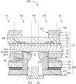
FIG. 3 , thedisplay panel 10 includes anupper polarizer 11, an upperadhesive layer 12, aCF substrate 13, aliquid crystal layer 14, aTFT array substrate 15, a loweradhesive layer 16, and alower polarizer 17. - The
TFT array substrate 15 is opposite to theCF substrate 13. Theliquid crystal layer 14 is between theTFT array substrate 15 and theCF substrate 13. Theupper polarizer 11 is on a side of theCF substrate 13 away from theTFT array substrate 15. The upperadhesive layer 12 is between theCF substrate 13 and theupper polarizer 11. TheCF substrate 13 and theupper polarizer 11 are bonded together by the upperadhesive layer 12. Thelower polarizer 17 is on theTFT array substrate 15 away from theCF substrate 13. The loweradhesive layer 16 is between theTFT array substrate 15 and thelower polarizer 17. TheTFT array substrate 15 and thelower polarizer 17 are bonded together by the loweradhesive layer 16. - The
TFT array substrate 15 includes a transparent first substrate (not shown), and a TFT array layer (not shown) on a side of the first substrate close to theCF substrate 13. The TFT array layer includes, for example, TFTs, scan lines, data lines, and the like. Pixel electrodes (not shown) and common electrodes (not shown) are also provided in the display area A1. Each sub-pixel includes one TFT and one pixel electrode electrically connected to the TFT. The pixel electrodes and the common electrodes are in the display area A1 and rotate the liquid crystal molecules in theliquid crystal layer 14 to form images for display. - In one embodiment, the
CF substrate 13 includes a transparent second substrate (not shown), and a color filter layer (not shown) on a side of the second substrate near the TFT array substrate15 (not shown), a black matrix (BM) (not shown), a protective layer (not shown), and so on. The CF layer includes, for example, a red filter layer in a red subpixel area, a green filter layer in a green subpixel area, and a blue filter layer in a blue subpixel area. The black matrix is between adjacent sub-pixels to prevent crosstalk of the primary color light emitted from the adjacent sub-pixels. - As shown in
FIG. 3 , thelower polarizer 17 defines a first throughhole 172. The first throughhole 172 penetrates the loweradhesive layer 16. The first throughhole 172 is aligned with the light transmission area A2 along a thickness direction of thedisplay device 100. Theupper polarizer 11 defines a second throughhole 112. The second throughhole 112 penetrates theupper adhesive layer 12. The second throughhole 112 is aligned with the light transmission area A2 along the thickness direction of thedisplay device 100. In one embodiment, a material of the upper and the loweradhesive layer - As shown in
FIG. 3 , thebacklight module 20 is on a side of thedisplay panel 10 away from itsdisplay surface 10a. Thebacklight module 20 includes aback plate 26 configured for carrying optical components of thebacklight module 20. Theback plate 26 includes a flat plate-shapedbottom plate 22 substantially parallel to thedisplay panel 10 and aframe 21 connected to thebottom plate 22. Theframe 21 is shaped to define an inner wall of the the mountinghole 212 extending to abut against a surface of theTFT array substrate 15. Theframe 21 is opaque, to preventing the light of thebacklight module 20 from leaking out from theframe 21. A material of theframe 21 is, for example, a metal or an alloy. - In other embodiments, the
frame 21 and thebottom plate 22 may be integrally formed. That is, theframe 21 is formed by bending thebottom plate 22 and extending in a direction toward thedisplay panel 10. - As shown in
FIG. 3 , theframe 21 is substantially perpendicular to thedisplay panel 10. Theframe 21 defines a mountinghole 212 penetrating thebacklight module 20. The mountinghole 212 is aligned with the light shielding area A3 along the thickness direction of thedisplay device 100. That is, the inner wall of the mountinghole 212 is in the light shielding area A3. Thecamera module 30 is embedded in the mountinghole 212 to reduce the thickness of thedisplay device 100. A size of the mountinghole 212 is larger than or substantially equal to a size of the lens of thecamera module 30. - The optical components of the
backlight module 20 include a light source (not shown), areflection sheet 23, alight guide plate 24, anoptical film group 25, and so on. Thereflection sheet 23, thelight guide plate 24, and theoptical film group 25 are sequentially stacked as stated on thebottom plate 22 in a direction close to thedisplay panel 10. Thereflection sheet 23, thelight guide plate 24, and theoptical film group 25 are basically flat plates. The mountinghole 212 penetrates thereflection sheet 23, thelight guide plate 24, and theoptical film group 25. That is, thereflection sheet 23, thelight guide plate 24, and theoptical film group 25 are all designed with openings. and surround theframe 21 of thebacklight module 20. - In one embodiment, the
backlight module 20 may be a direct type backlight module or an edge type backlight module. The light source may be a light-emitting diode. Theoptical film group 25 includes, for example, a diffusion sheet (not shown) or a brightness enhancement film (not shown). - As shown in
FIG. 3 , thedisplay panel 10 includes a firstlight shielding material 41 on a side of theTFT array substrate 15 away from theCF substrate 13. The firstlight shielding material 41 is aligned with the light shielding area A3 and surrounds the light transmission area A2. At least part of the firstlight shielding material 41 is in the first throughhole 172 for absorbing light from thelower polarizer 17 away from theTFT array substrate 15 toward the light transmission area A2. - The first
light shielding material 41 includes a firsthorizontal portion 41a, abent portion 41b, and a secondhorizontal portion 41c. The firsthorizontal portion 41apartially covers a surface of the TFT array substrate15 (i.e., the first substrate). Thebent portion 41bextends from the firsthorizontal portion 41aand covers sidewalls of the first throughhole 172. The secondhorizontal portion 41cextends from thebent portion 41bin a direction away from the light transmission area A2 of theframe 21, and covers a surface of thelower polarizer 17 away from the TFT array substrate15 (i.e., the first substrate). The firstlight shielding material 41 has light absorbing property, thereby preventing the light of thebacklight module 20 from leaking out from an area where thedisplay panel 10 and thebacklight module 20 are combined. - In one embodiment, the projection of the
frame 21 along the thickness direction of thedisplay device 100 falls within a projection of the first throughhole 172. The firsthorizontal portion 41aextends beyond theframe 21, in a direction in which theframe 21 approaches the light transmission area A2. The secondhorizontal portion 41cextends beyond theframe 21 in a direction in which theframe 21 is away from the light transmission area A2. That is, the left and right ends of the firstlight shielding material 41 extend beyond theframe 21, so that a size of the firstlight shielding material 41 is as large as possible to absorb more light entering the light shielding area A3 and the light transmission area A2. - In one embodiment, a material of the first
light shielding material 41 may be, but is not limited to, ink, glue, and so on. If the material of the firstlight shielding material 41 is a light shielding ink (e.g., a black ink) with a high optical density (OD) value, its thickness is in a range from 5 microns to 15 microns. - As shown in
FIG. 3 , theCF substrate 13 includes a secondlight shielding material 42. The secondlight shielding material 42 is aligned with the light shielding area A3 and surrounds the light transmission area A2. The secondlight shielding material 42 is in the shape of a ring. In other embodiments, the secondlight shielding material 42 may have other various shapes. - In one embodiment, in order to simplify manufacturing process, the second
light shielding material 42 and the black matrix are made of one material and formed by one patterning process (e.g., wet etching). In other embodiments, the secondlight shielding material 42 and the black matrix may be made independently, and the materials of the two may be different. - In one embodiment, an inner wall of the second through
hole 112 is between an inner side surface of the secondlight shielding material 42 near the light transmission area A2 and an outer side surface of the secondlight shielding material 42 near the display area A1. That is, a projection of the inner wall of the second throughhole 112 along the thickness direction of thedisplay device 100 is within a projection of the secondlight shielding material 42 to ensure the light shielding effect. - In one embodiment, the
display device 100 includes a firstlight shielding portion 51. The firstlight shielding portion 51 is in direct contact with thedisplay panel 10 and theframe 21 to fix them. The firstlight shielding portion 51 is aligned with the light shielding area A3 and surrounds the light transmission area A2 to absorb light that is incident from thebacklight module 20 into the light transmission area A2 and the light shielding area A3. That is, the firstlight shielding portion 51 cooperates with the first and the secondlight shielding material display panel 10 and thebacklight module 20. - In one embodiment, a gap G is defined between the
frame 21 and the firstlight shielding material 41. The firstlight shielding portion 51 is at least in the gap G That is, theframe 21 of thebacklight module 20 is abutted against the firstlight shielding portion 51. In this case, a material of the firstlight shielding portion 51 may be an elastic glue, which has a certain buffering effect. After thedisplay panel 10 and thebacklight module 20 are assembled, the elastic glue serves as a link and a buffer preventing separation of thedisplay panel 10 from thebacklight module 20, and preventing cracking and failure of the first substrate (which is made of glass). In addition, the elastic compression deformation of the elastic glue prevents light leakage in the dark state due to an assembly process error between thedisplay panel 10 and thebacklight module 20. - In one embodiment, the first
light shielding portion 51 extends from the gap G to a surface of theframe 21 near the light transmission area A2 and is in contact with the surface of theframe 21 near thedisplay panel 10. Therefore, on the basis of maximally absorbing the light emitted from thebacklight module 20 into the light shielding area A3 and the light transmission area A2, contact area of the firstlight shielding portion 51 and theframe 21 is increased, thus the fixing effect between thedisplay panel 10 and thebacklight module 20 is improved. - In one embodiment, a side surface of the first
horizontal portion 41anear the light transmission area A2 and a side surface of the firstlight shielding portion 51 near the light transmission area A2 may be overlapped or staggered. That is, the firstlight shielding portion 51 may cover the side surface of the firsthorizontal portion 41anear the light transmission area A2 and contact the TFT array substrate15 (the first substrate) (as shown inFIG. 3 ) to further increase the contact area between the firstlight shielding portion 51 and thedisplay panel 10, thus the fixing effect between thedisplay panel 10 and thebacklight module 20 is further improved. The firstlight shielding portion 51 may not exceed the side surface of the firsthorizontal portion 41anear the light transmission area A2. The projection of the firstlight shielding material 41 along the thickness direction of thedisplay device 100 coincides with the light shielding area A3, or the projection of the firstlight shielding material 41 is in all the shading areas A3. - The first
light shielding material 41 and the firstlight shielding portion 51 mainly absorb the light emitted by thebacklight module 20 into the light shielding area A3 and the light transmission area A2, and the secondlight shielding material 42 mainly absorbs light emitted through theliquid crystal layer 14 into the light shielding area A3. - In addition, in order to avoid light leakage to the light transmission area A2, the projections of the first and the second
light shielding material light shielding portion 51 are superposed along the thickness direction of thedisplay device 100 to cover the light shielding area A3. That is, the inner and outer edges of the area where the projections of the first and the secondlight shielding material light shielding portion 51 are superimposed are the inner edge of the light shielding area A3 near the light transmission area A2 and the outer edge of the light shielding area A3 near the display area A1. Therefore, the projections of the firstlight shielding material 41 along the thickness direction of thedisplay device 100, the secondlight shielding material 42, and the firstlight shielding portion 51 may cover a part of the light shielding area A3, and may also cover the entire area of the light shielding area A3. It is sufficient to ensure that the projection superposition of the three completely covers the light shielding area A3. - In one embodiment, the material of the first
light shielding material 41 is ink, and the material of the firstlight shielding portion 51 is elastic glue. When assembling thedisplay panel 10 and thebacklight module 20, only one inkjet process and one coating process are required. Compared with the case where the colloid is applied multiple times (at least twice) at the junction of thedisplay panel 10 and thebacklight module 20, the manufacturing tolerance of this method is small, and the manufacturing process is simplified. - In the
display device 100, the light shielding area A3 is between the display area A1 and the light transmission area A2, and the firstlight shielding material 41 is arranged to correspond to the light shielding area A3. The light from thebacklight module 20 toward the light shielding area A3 and the light transmission area A2 can be absorbed by the firstlight shielding material 41. Thecamera module 30 is aligned with the light transmission area A2 surrounded by the display area A1, without opening a through hole in thedisplay panel 10 to set up a special area for placing thecamera module 30, thereby increasing the screen ratio of thedisplay device 100. - In addition, in the
display device 100, theCF substrate 13 is further provided with the secondlight shielding material 42 corresponding to the light shielding area A3. The secondlight shielding material 42 absorbs light that has entered the light shielding area A3 after passing through theliquid crystal layer 14, and prevents light from the display area A1 from leaking into the light transmission area A2, thereby ensuring a display effect and an imaging effect. - Further, in the
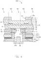
display device 100, by providing the firstlight shielding portion 51, the light emitted from thebacklight module 20 toward the light shielding area A3 and the light transmission area A2 can be further absorbed, and thebacklight module 20 and thedisplay panel 10 can be bonded. FIG. 4 shows adisplay device 200. As shown inFIG. 4 , a difference between thedisplay device 200 and thedisplay device 100 is that a size of an opening defined by the loweradhesive layer 16 of thedisplay device 200 is larger than a size of an opening of thelower polarizer 17 of thedisplay device 200. In thedisplay device 200, the firstlight shielding material 41 is between theTFT array substrate 15 and the lower polarized17. Thedisplay device 200 further includes a secondlight shielding portion 52 between thelower polarizer 17 and theframe 21. The secondlight shielding portion 52 is aligned with the light shielding area A3 and surrounds the light transmission area A2. The secondlight shielding portion 52 along a direction of theframe 21 away from the light transmission area A2 extends beyond theframe 21.- In one embodiment, the material of the lower
adhesive layer 16 is PSA, the material of the firstlight shielding material 41 is ink, the material of the firstlight shielding portion 51 is elastic glue, and the material of the secondlight shielding portion 52 is a double-sided tape. - During the manufacturing process, a pre-assembled liquid crystal display panel (mainly including a
TFT array substrate 15, aCF substrate 13, and a liquid crystal layer14) is provided. The surface of theTFT array substrate 15 away from theCF substrate 13 and correspondingly the light shielding area A3 is printed with ink to form a firstlight shielding material 41. PSA glue is attached to form the loweradhesive layer 16. Thelower polarizer 17 is attached, and double-sided adhesive is attached to theframe 21 of thebacklight module 20 to form the secondlight shielding portion 52. Thebacklight module 20 with the secondlight shielding portion 52 is attached to the liquid crystal display panel; and an elastic glue is applied to form the firstlight shielding portion 51. - In another embodiment, the second
light shielding portion 52 may be in direct contact with theoptical film group 25. That is, there is no gap between the secondlight shielding portion 52 and theoptical film group 25. During the manufacturing process, a double-sided tape is attached to theoptical film group 25 and theframe 21 to form the secondlight shielding portion 52. - The
frame 21 of thebacklight module 20 abuts against the second light shielding portion52 (that is, theframe 21 is in direct contact with the second light shielding portion52), and there is a gap G between the secondlight shielding portion 52 and the firstlight shielding material 41. The firstlight shielding portion 51 fills the gap G and directly contacts the surface of theTFT array substrate 15, a side surface of the secondlight shielding portion 52 near the light transmission area A2, and s side surface of theframe 21 defining the mountinghole 212. Therefore, on the basis of maximally absorbing the light emitted from thebacklight module 20 into the light shielding area A3 and the light transmission area A2, the contact area between the firstlight shielding portion 51 and thedisplay panel 10 is further increased, thus the fixing effect between thedisplay panel 10 and thebacklight module 20 is improved. - In the
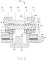
display device 200, the secondlight shielding portion 52 cooperates with the first and the secondlight shielding material light shielding portion 51 to absorb as much light as possible to avoid light leakage. FIG. 5 shows adisplay device 300. As shown inFIG. 5 , a difference between thedisplay device 300 and thedisplay device 100 is that a material of the loweradhesive layer 16 of thedisplay device 300 is soft glue. The projection of theframe 21 along the thickness direction of thedisplay device 100 at least partially overlaps thelower polarizer 17. That is, the size of the mountinghole 212 is equal to or larger than the size of the first throughhole 172. Since the material of the loweradhesive layer 16 is soft glue, it has a certain buffering effect. After thedisplay panel 10 and thebacklight module 20 are assembled, theframe 21 contacts the firstlight shielding material 41, the force of theframe 21 on thedisplay panel 10 can be released by compressing the soft glue. The dark light leakage problem caused by theframe 21 compressing the liquid crystal cell gap is avoided.- In one embodiment, the lower
adhesive layer 16 is an optically clear adhesive (OCA), and the loweradhesive layer 16 and thelower polarizer 17 may be sequentially attached to theTFT array substrate 15. Thelower polarizer 17 with the loweradhesive layer 16 is then attached to theTFT array substrate 15. FIG. 6 shows adisplay device 400. As shown inFIG. 6 , a difference between thedisplay device 400 and thedisplay device 200 is that the material of the loweradhesive layer 16 is soft glue. The projection of theframe 21 along the thickness direction of thedisplay device 400 at least partially overlaps thelower polarizer 17. That is, the size of the mountinghole 212 is equal to or larger than the size of the first throughhole 172. Since the material of the loweradhesive layer 16 is soft glue, it has a certain buffering effect. After thedisplay panel 10 and thebacklight module 20 are assembled, theframe 21 contacts the firstlight shielding material 41, the force of theframe 21 on thedisplay panel 10 can be released by compressing the soft glue. The dark light leakage problem caused by theframe 21 compressing the the liquid crystal cell gap is avoided.- In one embodiment, the material of the lower
adhesive layer 16 is an OCA, the material of the firstlight shielding material 41 and the secondlight shielding portion 52 is ink, and the material of the firstlight shielding portion 51 is an elastic glue. The side surface of the secondlight shielding portion 52 near the light transmission area A2 does not exceed the side surface of thelower polarizer 17 defining the first throughhole 172. During the manufacturing process, a pre-assembled liquid crystal display panel (mainly including aTFT array substrate 15, aCF substrate 13, and a liquid crystal layer14) is provided. The surface of theTFT array substrate 15 away from theCF substrate 13 and correspondingly the light shielding area A3 is printed with ink to form the firstlight shielding material 41. The loweradhesive layer 16 and thelower polarizer 17 are sequentially attached to theTFT array substrate 15. - Alternatively, the
lower polarizer 17 with the loweradhesive layer 16 is provided, and thelower polarizer 17 with the loweradhesive layer 16 is attached to theTFT array substrate 15. The surface of thelower polarizer 17 away from the loweradhesive layer 16 is printed with ink to form the secondlight shielding portion 52. Thebacklight module 20 is assembled. The elastic glue is applied to form the firstlight shielding portion 51. - The display device100 (200,300,400) may be any product or component having a display function, such as a mobile phone, a liquid crystal display, a liquid crystal television, a tablet computer, a digital photo frame, a wearable device, and so on.
- It is to be understood, even though information and advantages of the present exemplary embodiments have been set forth in the foregoing description, together with details of the structures and functions of the present exemplary embodiments, the disclosure is illustrative only. Changes may be made in detail, especially in matters of shape, size, and arrangement of parts within the principles of the present exemplary embodiments to the full extent indicated by the plain meaning of the terms in which the appended claims are expressed.
Claims (12)
Priority Applications (1)
| Application Number | Priority Date | Filing Date | Title |
|---|---|---|---|
| US16/702,999US11057556B2 (en) | 2018-12-07 | 2019-12-04 | Display panel and display device using same |
Applications Claiming Priority (2)
| Application Number | Priority Date | Filing Date | Title |
|---|---|---|---|
| US201862776470P | 2018-12-07 | 2018-12-07 | |
| US16/702,999US11057556B2 (en) | 2018-12-07 | 2019-12-04 | Display panel and display device using same |
Publications (2)
| Publication Number | Publication Date |
|---|---|
| US20200186688A1true US20200186688A1 (en) | 2020-06-11 |
| US11057556B2 US11057556B2 (en) | 2021-07-06 |
Family
ID=69750122
Family Applications (1)
| Application Number | Title | Priority Date | Filing Date |
|---|---|---|---|
| US16/702,999ActiveUS11057556B2 (en) | 2018-12-07 | 2019-12-04 | Display panel and display device using same |
Country Status (3)
| Country | Link |
|---|---|
| US (1) | US11057556B2 (en) |
| CN (2) | CN110888261A (en) |
| TW (1) | TWI719738B (en) |
Cited By (31)
| Publication number | Priority date | Publication date | Assignee | Title |
|---|---|---|---|---|
| CN109976061A (en)* | 2019-04-29 | 2019-07-05 | 武汉华星光电技术有限公司 | Display panel and display device |
| CN112034649A (en)* | 2020-09-15 | 2020-12-04 | 京东方科技集团股份有限公司 | Display panel and electronic device |
| US10866461B2 (en)* | 2019-03-14 | 2020-12-15 | Sharp Kabushiki Kaisha | Image display device |
| US10877207B1 (en)* | 2019-11-11 | 2020-12-29 | Wuhan China Star Optoelectronics Technology Co., Ltd. | Backlight module and display device |
| US20210026046A1 (en)* | 2019-07-22 | 2021-01-28 | Samsung Display Co., Ltd. | Window member, electronic apparatus including the same, and manufacturing method of window member |
| CN112363345A (en)* | 2020-11-10 | 2021-02-12 | 京东方科技集团股份有限公司 | Color film substrate, display module, display panel and display device |
| US10996503B2 (en)* | 2019-09-24 | 2021-05-04 | Wuhan China Star Optoelectronics Technology Co., Ltd. | Display device and method of manufacturing same |
| US20210193756A1 (en)* | 2019-12-18 | 2021-06-24 | Lg Display Co., Ltd. | Display device |
| US11057554B2 (en)* | 2017-05-22 | 2021-07-06 | Sharp Kabushiki Kaisha | Display device with hollowed part in backlight |
| US11106066B2 (en)* | 2019-03-11 | 2021-08-31 | Japan Display Inc. | Electro-optical device and electronic equipment |
| US11131890B2 (en)* | 2019-04-29 | 2021-09-28 | Beijing Xiaomi Mobile Software Co., Ltd. | LCD and display device |
| US20210405706A1 (en)* | 2020-06-24 | 2021-12-30 | Samsung Display Co., Ltd. | Electronic device |
| US20220026771A1 (en)* | 2018-12-13 | 2022-01-27 | Honor Device Co., Ltd. | Display Assembly, Display Device and Driving Method Therefor |
| US11258040B2 (en)* | 2019-04-12 | 2022-02-22 | Samsung Display Co., Ltd. | Display device |
| US11307459B2 (en)* | 2020-05-07 | 2022-04-19 | Innolux Corporation | Display device comprising a switchable diffuser and a backlight module having a first region and a second region, and a mobile device comprising the same |
| US20220279100A1 (en)* | 2019-11-18 | 2022-09-01 | Vivo Mobile Communication Co., Ltd. | Electronic device |
| US20220285656A1 (en)* | 2021-03-05 | 2022-09-08 | Samsung Display Co., Ltd. | Display device and method of manufacturing the same |
| US20220350230A1 (en)* | 2020-06-30 | 2022-11-03 | Boe Technology Group Co., Ltd. | Transparent Display Panel and Control Method and Apparatus Therefor, Display Apparatus, and Display System |
| US20230097654A1 (en)* | 2020-02-26 | 2023-03-30 | Wuhan China Star Optoelectronics Technology Co., Ltd | Display device |
| US20230176279A1 (en)* | 2020-04-23 | 2023-06-08 | JRD Communication (Shenzhen) Ltd. | Display panel and terminal |
| US11765945B2 (en)* | 2019-05-27 | 2023-09-19 | Samsung Display Co., Ltd. | Display device having a black matrix |
| US11785795B2 (en)* | 2020-02-14 | 2023-10-10 | Samsung Display Co., Ltd. | Display device including protective layer below substrate |
| EP4195649A4 (en)* | 2020-09-10 | 2024-01-31 | Samsung Electronics Co., Ltd. | Electronic device including camera module that takes photographs through at least part of display |
| US20240045134A1 (en)* | 2021-09-17 | 2024-02-08 | Wuhan China Star Optoelectronics Technology Co., Ltd. | Display panel and electronic device |
| TWI852105B (en)* | 2021-10-11 | 2024-08-11 | 美商雷亞有限公司 | Method, apparatus, device and storage medium for manufacturing a naked-eye 3d display device |
| US20240369871A1 (en)* | 2023-05-04 | 2024-11-07 | Interface Technology (Chengdu) Co., Ltd. | Touch display panel, display device, and method for manufacturing touch display panel |
| US12164346B2 (en)* | 2020-03-30 | 2024-12-10 | Samsung Display Co., Ltd. | Display apparatus |
| US12276876B2 (en)* | 2022-07-22 | 2025-04-15 | Wuhan China Star Optoelectronics Technology Co., Ltd. | Display device including driving mechanism |
| US12298624B2 (en)* | 2022-04-26 | 2025-05-13 | Beijing Boe Display Technology Co., Ltd. | Display device |
| US12310177B2 (en)* | 2021-07-13 | 2025-05-20 | Samsung Display Co., Ltd. | Display device with window having stack of transparent and light-blocking patterns, and method of manufacturing the same |
| US12443063B2 (en) | 2019-03-11 | 2025-10-14 | Magnolia White Corporation | Electro-optical device and electronic equipment |
Families Citing this family (18)
| Publication number | Priority date | Publication date | Assignee | Title |
|---|---|---|---|---|
| KR102603601B1 (en)* | 2018-08-13 | 2023-11-20 | 엘지디스플레이 주식회사 | Display device and manufacturing method of it |
| CN110888261A (en)* | 2018-12-07 | 2020-03-17 | 鸿富锦精密工业(深圳)有限公司 | Display panel and display device |
| KR20210003990A (en)* | 2019-07-02 | 2021-01-13 | 삼성디스플레이 주식회사 | Electronic apparatus and method of manufacturing the same |
| CN110837190A (en)* | 2019-10-29 | 2020-02-25 | 武汉华星光电技术有限公司 | Display device and manufacturing method thereof |
| KR102749504B1 (en)* | 2019-12-31 | 2025-01-03 | 삼성디스플레이 주식회사 | Display device and Method for manufacturing a display device |
| CN111402739B (en)* | 2020-03-31 | 2023-03-24 | 云谷(固安)科技有限公司 | Display module and preparation method thereof |
| CN111430422B (en)* | 2020-04-02 | 2023-06-20 | 合肥维信诺科技有限公司 | Display panel, manufacturing method thereof and display device |
| CN111443518A (en)* | 2020-04-07 | 2020-07-24 | 捷开通讯(深圳)有限公司 | Electronic device and driving method thereof |
| KR20210137856A (en)* | 2020-05-11 | 2021-11-18 | 삼성전자주식회사 | Electronic device including camera and display |
| CN111540271B (en)* | 2020-05-18 | 2022-06-17 | 昆山国显光电有限公司 | Display panels and display devices |
| CN111856809B (en)* | 2020-06-11 | 2023-01-06 | 友达光电(苏州)有限公司 | display module |
| CN111708208A (en)* | 2020-06-12 | 2020-09-25 | 深圳传音控股股份有限公司 | Display device |
| CN111610658B (en)* | 2020-06-24 | 2023-03-17 | 武汉天马微电子有限公司 | Display module, manufacturing method thereof and display device |
| CN111951671A (en)* | 2020-08-14 | 2020-11-17 | 武汉华星光电技术有限公司 | Display device and manufacturing method thereof |
| TWI710809B (en)* | 2020-08-17 | 2020-11-21 | 友達光電股份有限公司 | Light board device and manufacturing method thereof |
| CN112015008A (en)* | 2020-09-15 | 2020-12-01 | 武汉华星光电技术有限公司 | Backlight module, liquid crystal display panel and manufacturing method of liquid crystal display panel |
| CN117202720A (en)* | 2022-05-25 | 2023-12-08 | 中兴通讯股份有限公司 | Display screen, under-screen camera device and terminal equipment |
| CN119002121A (en)* | 2023-05-22 | 2024-11-22 | 京东方科技集团股份有限公司 | Backlight module, display module and display device |
Family Cites Families (37)
| Publication number | Priority date | Publication date | Assignee | Title |
|---|---|---|---|---|
| JP3733418B2 (en)* | 2001-04-16 | 2006-01-11 | シャープ株式会社 | Adhesive sheet, laminated sheet and liquid crystal display device |
| JP3875130B2 (en)* | 2002-03-26 | 2007-01-31 | 株式会社東芝 | Display device and manufacturing method thereof |
| US9143668B2 (en)* | 2010-10-29 | 2015-09-22 | Apple Inc. | Camera lens structures and display structures for electronic devices |
| US8467177B2 (en)* | 2010-10-29 | 2013-06-18 | Apple Inc. | Displays with polarizer windows and opaque masking layers for electronic devices |
| DE102011089443B4 (en)* | 2011-02-14 | 2016-12-01 | Lg Display Co., Ltd. | display device |
| KR101813459B1 (en)* | 2011-06-24 | 2018-01-02 | 엘지디스플레이 주식회사 | Display apparatus |
| US8867015B2 (en)* | 2012-01-11 | 2014-10-21 | Apple Inc. | Displays with liquid crystal shutters |
| KR102006775B1 (en)* | 2012-08-30 | 2019-08-02 | 엘지디스플레이 주식회사 | Liquid crystal panel and liquid crystal display device using the same |
| KR101998096B1 (en)* | 2012-09-03 | 2019-07-09 | 엘지디스플레이 주식회사 | Liquid crystal panel and liquid crystal display device using the same |
| US9075199B2 (en)* | 2012-10-30 | 2015-07-07 | Apple Inc. | Displays with polarizer layers for electronic devices |
| WO2015022887A1 (en)* | 2013-08-12 | 2015-02-19 | シャープ株式会社 | Display device |
| US9851605B2 (en)* | 2013-08-29 | 2017-12-26 | Sharp Kabushiki Kaisha | Display panel |
| JP6054582B2 (en)* | 2014-05-23 | 2016-12-27 | シャープ株式会社 | Lighting device and display device |
| KR102524754B1 (en)* | 2015-09-09 | 2023-04-21 | 엘지디스플레이 주식회사 | Display device |
| KR101717655B1 (en)* | 2015-11-30 | 2017-03-17 | 엘지디스플레이 주식회사 | Different form of display device having hole |
| KR102501111B1 (en)* | 2015-12-28 | 2023-02-16 | 엘지디스플레이 주식회사 | Camera module integrated liquid display device and manufacturing method thereof |
| JP2018004728A (en)* | 2016-06-28 | 2018-01-11 | 株式会社ジャパンディスプレイ | Display device and bonding method |
| CN106878564A (en)* | 2017-03-07 | 2017-06-20 | 广东欧珀移动通信有限公司 | Display control method and device, display screen and mobile terminal |
| SG11201909937XA (en)* | 2017-04-25 | 2019-11-28 | Huawei Tech Co Ltd | Lcd display, electronic device, lcd display manufacturing method |
| JP2019090941A (en)* | 2017-11-15 | 2019-06-13 | シャープ株式会社 | Display device |
| JP2019133097A (en)* | 2018-02-02 | 2019-08-08 | シャープ株式会社 | Image display device |
| JP2019184828A (en)* | 2018-04-10 | 2019-10-24 | シャープ株式会社 | Liquid crystal display |
| JP2019184827A (en)* | 2018-04-10 | 2019-10-24 | シャープ株式会社 | Liquid crystal display and method for manufacturing the same |
| US10690959B2 (en)* | 2018-04-26 | 2020-06-23 | Beijing Boe Optoelectronics Technology Co., Ltd. | Display apparatus |
| CN108919544A (en)* | 2018-06-26 | 2018-11-30 | Oppo广东移动通信有限公司 | Display screen assembly, electronic equipment and manufacturing method of electronic equipment |
| CN108873471A (en)* | 2018-06-28 | 2018-11-23 | Oppo广东移动通信有限公司 | Backlight module, display screen assembly and electronic equipment |
| CN108897174A (en)* | 2018-06-28 | 2018-11-27 | Oppo广东移动通信有限公司 | screen assembly and electronic device |
| CN108881543A (en)* | 2018-06-28 | 2018-11-23 | Oppo广东移动通信有限公司 | Display components and electronics |
| CN108681150B (en)* | 2018-06-29 | 2023-12-08 | 厦门天马微电子有限公司 | Backlight module and display device |
| CN108900672B (en)* | 2018-07-06 | 2021-05-04 | Oppo广东移动通信有限公司 | Electronic device and manufacturing method thereof |
| CN108681131B (en)* | 2018-07-27 | 2021-07-30 | 厦门天马微电子有限公司 | Display device |
| KR102598230B1 (en)* | 2018-08-13 | 2023-11-03 | 삼성디스플레이 주식회사 | Display device |
| KR102672833B1 (en)* | 2018-08-27 | 2024-06-05 | 엘지디스플레이 주식회사 | Display device |
| US10845664B2 (en)* | 2018-11-22 | 2020-11-24 | Wuhan China Star Optoelectronics Technology Co., Ltd. | Liquid crystal display panel and terminal device |
| CN110888261A (en)* | 2018-12-07 | 2020-03-17 | 鸿富锦精密工业(深圳)有限公司 | Display panel and display device |
| CN109541833A (en)* | 2018-12-13 | 2019-03-29 | 华为技术有限公司 | Display component, display device and its driving method |
| KR102803995B1 (en)* | 2019-04-03 | 2025-05-12 | 삼성디스플레이 주식회사 | Display apparatus and method of manufacturing the same |
- 2019
- 2019-12-03CNCN201911219570.9Apatent/CN110888261A/enactivePending
- 2019-12-03TWTW108144192Apatent/TWI719738B/enactive
- 2019-12-03CNCN201922156528.9Upatent/CN211180477U/enactiveActive
- 2019-12-04USUS16/702,999patent/US11057556B2/enactiveActive
Cited By (47)
| Publication number | Priority date | Publication date | Assignee | Title |
|---|---|---|---|---|
| US11057554B2 (en)* | 2017-05-22 | 2021-07-06 | Sharp Kabushiki Kaisha | Display device with hollowed part in backlight |
| US11796875B2 (en)* | 2018-12-13 | 2023-10-24 | Honor Device Co., Ltd. | Display assembly, display device and driving method therefor |
| US20220026771A1 (en)* | 2018-12-13 | 2022-01-27 | Honor Device Co., Ltd. | Display Assembly, Display Device and Driving Method Therefor |
| US20220236603A1 (en)* | 2019-03-11 | 2022-07-28 | Japan Display Inc. | Electro-optical device and electronic equipment |
| US12443063B2 (en) | 2019-03-11 | 2025-10-14 | Magnolia White Corporation | Electro-optical device and electronic equipment |
| US11719968B2 (en)* | 2019-03-11 | 2023-08-08 | Japan Display Inc. | Electro-optical device and electronic equipment |
| US12013604B2 (en) | 2019-03-11 | 2024-06-18 | Japan Display Inc. | Electro-optical device and electronic equipment |
| US11106066B2 (en)* | 2019-03-11 | 2021-08-31 | Japan Display Inc. | Electro-optical device and electronic equipment |
| US11333914B2 (en) | 2019-03-11 | 2022-05-17 | Japan Display Inc. | Electro-optical device and electronic equipment |
| US10866461B2 (en)* | 2019-03-14 | 2020-12-15 | Sharp Kabushiki Kaisha | Image display device |
| US11258040B2 (en)* | 2019-04-12 | 2022-02-22 | Samsung Display Co., Ltd. | Display device |
| US12133412B2 (en)* | 2019-04-12 | 2024-10-29 | Samsung Display Co., Ltd. | Display device |
| US20220271257A1 (en)* | 2019-04-12 | 2022-08-25 | Samsung Display Co., Ltd. | Display device |
| CN109976061A (en)* | 2019-04-29 | 2019-07-05 | 武汉华星光电技术有限公司 | Display panel and display device |
| US11131890B2 (en)* | 2019-04-29 | 2021-09-28 | Beijing Xiaomi Mobile Software Co., Ltd. | LCD and display device |
| US11765945B2 (en)* | 2019-05-27 | 2023-09-19 | Samsung Display Co., Ltd. | Display device having a black matrix |
| US20210026046A1 (en)* | 2019-07-22 | 2021-01-28 | Samsung Display Co., Ltd. | Window member, electronic apparatus including the same, and manufacturing method of window member |
| US12044866B2 (en)* | 2019-07-22 | 2024-07-23 | Samsung Display Co., Ltd. | Window member, electronic apparatus including the same, and manufacturing method of window member |
| US11592600B2 (en)* | 2019-07-22 | 2023-02-28 | Samsung Display Co., Ltd. | Window member, electronic apparatus including the same, and manufacturing method of window member |
| US10996503B2 (en)* | 2019-09-24 | 2021-05-04 | Wuhan China Star Optoelectronics Technology Co., Ltd. | Display device and method of manufacturing same |
| US10877207B1 (en)* | 2019-11-11 | 2020-12-29 | Wuhan China Star Optoelectronics Technology Co., Ltd. | Backlight module and display device |
| US20220279100A1 (en)* | 2019-11-18 | 2022-09-01 | Vivo Mobile Communication Co., Ltd. | Electronic device |
| US12069360B2 (en)* | 2019-11-18 | 2024-08-20 | Vivo Mobile Communication Co., Ltd. | Electronic device |
| US11626456B2 (en)* | 2019-12-18 | 2023-04-11 | Lg Display Co., Ltd. | Display device including stepped section substrate with embedded camera |
| US20210193756A1 (en)* | 2019-12-18 | 2021-06-24 | Lg Display Co., Ltd. | Display device |
| US12108650B2 (en)* | 2019-12-18 | 2024-10-01 | Lg Display Co., Ltd. | Display device including stepped section substrate with embedded camera |
| US20230209969A1 (en)* | 2019-12-18 | 2023-06-29 | Lg Display Co., Ltd. | Display device including stepped section substrate with embedded camera |
| US11785795B2 (en)* | 2020-02-14 | 2023-10-10 | Samsung Display Co., Ltd. | Display device including protective layer below substrate |
| US20230097654A1 (en)* | 2020-02-26 | 2023-03-30 | Wuhan China Star Optoelectronics Technology Co., Ltd | Display device |
| US11782302B2 (en)* | 2020-02-26 | 2023-10-10 | Wuhan China Star Optoelectronics Technology Co., Ltd | Display device |
| US12164346B2 (en)* | 2020-03-30 | 2024-12-10 | Samsung Display Co., Ltd. | Display apparatus |
| US20230176279A1 (en)* | 2020-04-23 | 2023-06-08 | JRD Communication (Shenzhen) Ltd. | Display panel and terminal |
| US11307459B2 (en)* | 2020-05-07 | 2022-04-19 | Innolux Corporation | Display device comprising a switchable diffuser and a backlight module having a first region and a second region, and a mobile device comprising the same |
| US20210405706A1 (en)* | 2020-06-24 | 2021-12-30 | Samsung Display Co., Ltd. | Electronic device |
| US11994790B2 (en)* | 2020-06-30 | 2024-05-28 | Beijing Boe Display Technology Co., Ltd. | Transparent display panel and control method and apparatus therefor, display apparatus, and display system |
| US20220350230A1 (en)* | 2020-06-30 | 2022-11-03 | Boe Technology Group Co., Ltd. | Transparent Display Panel and Control Method and Apparatus Therefor, Display Apparatus, and Display System |
| EP4195649A4 (en)* | 2020-09-10 | 2024-01-31 | Samsung Electronics Co., Ltd. | Electronic device including camera module that takes photographs through at least part of display |
| CN112034649A (en)* | 2020-09-15 | 2020-12-04 | 京东方科技集团股份有限公司 | Display panel and electronic device |
| CN112363345A (en)* | 2020-11-10 | 2021-02-12 | 京东方科技集团股份有限公司 | Color film substrate, display module, display panel and display device |
| US20220285656A1 (en)* | 2021-03-05 | 2022-09-08 | Samsung Display Co., Ltd. | Display device and method of manufacturing the same |
| US12310177B2 (en)* | 2021-07-13 | 2025-05-20 | Samsung Display Co., Ltd. | Display device with window having stack of transparent and light-blocking patterns, and method of manufacturing the same |
| US11947156B2 (en)* | 2021-09-17 | 2024-04-02 | Wuhan China Star Optoelectronics Technology Co., Ltd. | Display panel and electronic device |
| US20240045134A1 (en)* | 2021-09-17 | 2024-02-08 | Wuhan China Star Optoelectronics Technology Co., Ltd. | Display panel and electronic device |
| TWI852105B (en)* | 2021-10-11 | 2024-08-11 | 美商雷亞有限公司 | Method, apparatus, device and storage medium for manufacturing a naked-eye 3d display device |
| US12298624B2 (en)* | 2022-04-26 | 2025-05-13 | Beijing Boe Display Technology Co., Ltd. | Display device |
| US12276876B2 (en)* | 2022-07-22 | 2025-04-15 | Wuhan China Star Optoelectronics Technology Co., Ltd. | Display device including driving mechanism |
| US20240369871A1 (en)* | 2023-05-04 | 2024-11-07 | Interface Technology (Chengdu) Co., Ltd. | Touch display panel, display device, and method for manufacturing touch display panel |
Also Published As
| Publication number | Publication date |
|---|---|
| CN211180477U (en) | 2020-08-04 |
| TW202032231A (en) | 2020-09-01 |
| CN110888261A (en) | 2020-03-17 |
| US11057556B2 (en) | 2021-07-06 |
| TWI719738B (en) | 2021-02-21 |
Similar Documents
| Publication | Publication Date | Title |
|---|---|---|
| US11057556B2 (en) | Display panel and display device using same | |
| US10890794B2 (en) | Display device | |
| CN108628043B (en) | Screen components and electronic devices | |
| CN108153071B (en) | Display panel, manufacturing method thereof and display device | |
| CN210465917U (en) | Liquid crystal display device having a plurality of pixel electrodes | |
| CN101641634B (en) | Liquid crystal display panel with microlens array and method for manufacturing the same | |
| US8228479B2 (en) | Liquid crystal display with spacers arranged corresponding to metal electrode pedestals | |
| KR101279119B1 (en) | Liquid Crystal Display | |
| CN210465916U (en) | Liquid crystal display device having a plurality of pixel electrodes | |
| US10001676B2 (en) | Display device | |
| US11320697B2 (en) | Display device comprising a bendable light-transmissive layer and manufacturing method thereof | |
| JP2008242307A (en) | LCD panel with microlens array | |
| CN110796954A (en) | Display module, manufacturing method thereof and display device | |
| US20200174310A1 (en) | Liquid crystal display device | |
| KR101830242B1 (en) | Liquid crystal display device | |
| CN109946871A (en) | display device | |
| JP5659294B2 (en) | Display device | |
| CN103941474A (en) | A kind of manufacturing method of light-shielding tape and its backlight module | |
| US20200241358A1 (en) | Display assembly and display device | |
| JP5213616B2 (en) | Liquid crystal device, method for manufacturing liquid crystal device, and electronic apparatus | |
| CN101510033B (en) | Liquid crystal display device | |
| WO2010106709A1 (en) | Active matrix substrate and display device | |
| US20100053031A1 (en) | Electro-optical device and electronic apparatus | |
| CN110967856A (en) | Display module, manufacturing method thereof and display device | |
| JP2011191475A (en) | Electro-optic device and method for manufacturing the same, and electronic equipment |
Legal Events
| Date | Code | Title | Description |
|---|---|---|---|
| AS | Assignment | Owner name:HON HAI PRECISION INDUSTRY CO., LTD., TAIWAN Free format text:ASSIGNMENT OF ASSIGNORS INTEREST;ASSIGNORS:CHEN, CHUAN-KUN;HUANG, LI-CHIAO;REEL/FRAME:051176/0489 Effective date:20191202 | |
| FEPP | Fee payment procedure | Free format text:ENTITY STATUS SET TO UNDISCOUNTED (ORIGINAL EVENT CODE: BIG.); ENTITY STATUS OF PATENT OWNER: LARGE ENTITY | |
| STPP | Information on status: patent application and granting procedure in general | Free format text:NON FINAL ACTION MAILED | |
| STPP | Information on status: patent application and granting procedure in general | Free format text:RESPONSE TO NON-FINAL OFFICE ACTION ENTERED AND FORWARDED TO EXAMINER | |
| STPP | Information on status: patent application and granting procedure in general | Free format text:NOTICE OF ALLOWANCE MAILED -- APPLICATION RECEIVED IN OFFICE OF PUBLICATIONS | |
| STPP | Information on status: patent application and granting procedure in general | Free format text:PUBLICATIONS -- ISSUE FEE PAYMENT RECEIVED | |
| STPP | Information on status: patent application and granting procedure in general | Free format text:PUBLICATIONS -- ISSUE FEE PAYMENT VERIFIED | |
| STCF | Information on status: patent grant | Free format text:PATENTED CASE | |
| MAFP | Maintenance fee payment | Free format text:PAYMENT OF MAINTENANCE FEE, 4TH YEAR, LARGE ENTITY (ORIGINAL EVENT CODE: M1551); ENTITY STATUS OF PATENT OWNER: LARGE ENTITY Year of fee payment:4 |