US20200140263A1 - Reduced mems cavity gap - Google Patents
Reduced mems cavity gapDownload PDFInfo
- Publication number
- US20200140263A1 US20200140263A1US16/408,239US201916408239AUS2020140263A1US 20200140263 A1US20200140263 A1US 20200140263A1US 201916408239 AUS201916408239 AUS 201916408239AUS 2020140263 A1US2020140263 A1US 2020140263A1
- Authority
- US
- United States
- Prior art keywords
- wafer
- mems
- cap
- mems device
- cavity
- Prior art date
- Legal status (The legal status is an assumption and is not a legal conclusion. Google has not performed a legal analysis and makes no representation as to the accuracy of the status listed.)
- Granted
Links
Images


Classifications
- B—PERFORMING OPERATIONS; TRANSPORTING
- B81—MICROSTRUCTURAL TECHNOLOGY
- B81C—PROCESSES OR APPARATUS SPECIALLY ADAPTED FOR THE MANUFACTURE OR TREATMENT OF MICROSTRUCTURAL DEVICES OR SYSTEMS
- B81C1/00—Manufacture or treatment of devices or systems in or on a substrate
- B81C1/00015—Manufacture or treatment of devices or systems in or on a substrate for manufacturing microsystems
- B81C1/00261—Processes for packaging MEMS devices
- B81C1/00269—Bonding of solid lids or wafers to the substrate
- B—PERFORMING OPERATIONS; TRANSPORTING
- B81—MICROSTRUCTURAL TECHNOLOGY
- B81C—PROCESSES OR APPARATUS SPECIALLY ADAPTED FOR THE MANUFACTURE OR TREATMENT OF MICROSTRUCTURAL DEVICES OR SYSTEMS
- B81C1/00—Manufacture or treatment of devices or systems in or on a substrate
- B81C1/00015—Manufacture or treatment of devices or systems in or on a substrate for manufacturing microsystems
- B81C1/00023—Manufacture or treatment of devices or systems in or on a substrate for manufacturing microsystems without movable or flexible elements
- B81C1/00047—Cavities
- B—PERFORMING OPERATIONS; TRANSPORTING
- B81—MICROSTRUCTURAL TECHNOLOGY
- B81B—MICROSTRUCTURAL DEVICES OR SYSTEMS, e.g. MICROMECHANICAL DEVICES
- B81B7/00—Microstructural systems; Auxiliary parts of microstructural devices or systems
- B81B7/02—Microstructural systems; Auxiliary parts of microstructural devices or systems containing distinct electrical or optical devices of particular relevance for their function, e.g. microelectro-mechanical systems [MEMS]
- B—PERFORMING OPERATIONS; TRANSPORTING
- B81—MICROSTRUCTURAL TECHNOLOGY
- B81C—PROCESSES OR APPARATUS SPECIALLY ADAPTED FOR THE MANUFACTURE OR TREATMENT OF MICROSTRUCTURAL DEVICES OR SYSTEMS
- B81C1/00—Manufacture or treatment of devices or systems in or on a substrate
- B81C1/00436—Shaping materials, i.e. techniques for structuring the substrate or the layers on the substrate
- B81C1/00523—Etching material
- B81C1/00531—Dry etching
- B—PERFORMING OPERATIONS; TRANSPORTING
- B81—MICROSTRUCTURAL TECHNOLOGY
- B81B—MICROSTRUCTURAL DEVICES OR SYSTEMS, e.g. MICROMECHANICAL DEVICES
- B81B2203/00—Basic microelectromechanical structures
- B81B2203/03—Static structures
- B81B2203/0315—Cavities
- B—PERFORMING OPERATIONS; TRANSPORTING
- B81—MICROSTRUCTURAL TECHNOLOGY
- B81C—PROCESSES OR APPARATUS SPECIALLY ADAPTED FOR THE MANUFACTURE OR TREATMENT OF MICROSTRUCTURAL DEVICES OR SYSTEMS
- B81C2201/00—Manufacture or treatment of microstructural devices or systems
- B81C2201/01—Manufacture or treatment of microstructural devices or systems in or on a substrate
- B81C2201/0101—Shaping material; Structuring the bulk substrate or layers on the substrate; Film patterning
- B81C2201/0128—Processes for removing material
- B81C2201/013—Etching
- B81C2201/0132—Dry etching, i.e. plasma etching, barrel etching, reactive ion etching [RIE], sputter etching or ion milling
- B—PERFORMING OPERATIONS; TRANSPORTING
- B81—MICROSTRUCTURAL TECHNOLOGY
- B81C—PROCESSES OR APPARATUS SPECIALLY ADAPTED FOR THE MANUFACTURE OR TREATMENT OF MICROSTRUCTURAL DEVICES OR SYSTEMS
- B81C2203/00—Forming microstructural systems
- B81C2203/03—Bonding two components
- B81C2203/033—Thermal bonding
- B81C2203/036—Fusion bonding
Definitions
- MEMSmicro-electro-mechanical systems
- MEMS devicesare a class of devices that are fabricated using semiconductor-like processes and exhibit mechanical characteristics.
- MEMS devicesmay include the ability to move or deform. In many cases, but not always, MEMS interact with electrical signals.
- a MEMS devicemay refer to a semiconductor device that is implemented as a micro-electro-mechanical system.
- a MEMS deviceincludes mechanical elements and may optionally include electronics (e.g. electronics for sensing).
- MEMS devicesinclude but are not limited to, for example, gyroscopes, accelerometers, magnetometers, pressure sensors, etc. As technology advances, it is desirable to reduce the size of the MEMS devices, thereby resulting in die size reduction.
- a methodincluding forming a MEMS cap wafer.
- a cavityis formed in the MEMS cap wafer, and a bond material is deposited on the MEMS cap wafer, wherein the bond material lines the cavity after the depositing.
- the MEMS cap waferis bonded to a MEMS device wafer, wherein the bond material forms a bond between the MEMS cap wafer and the MEMS device wafer.
- a MEMS deviceis formed in the MEMS device wafer. The bond material is removed from the cavity.
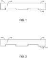
- FIG. 1shows a cap wafer including cap cavities according to one aspect of the present embodiments.
- FIG. 2shows an oxide formed on the first side and the cap cavity according to one aspect of the present embodiments.
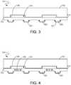
- FIG. 3shows the cap wafer fusion bonded to a MEMS device wafer including standoffs according to one aspect of the present embodiments.
- FIG. 4shows the formation of the MEMS device according to one aspect of the present embodiments.
- FIG. 5shows the removal of the bond in the cap cavity according to one aspect of the present embodiments.
- FIG. 6shows eutectic bonding of the MEMS wafer to a CMOS wafer according to one aspect of the present embodiments.
- FIG. 7shows an exemplary flow diagram for removing the bond material from the cavity according to one aspect of the present embodiments.
- ordinal numberse.g., first, second, third, etc. are used to distinguish or identify different elements or steps in a group of elements or steps, and do not supply a serial or numerical limitation on the elements or steps of the embodiments thereof.
- first, second, and “third” elements or stepsneed not necessarily appear in that order, and the embodiments thereof need not necessarily be limited to three elements or steps.
- any labelssuch as “left,” “right,” “front,” “back,” “top,” “middle,” “bottom,” “beside,” “forward,” “reverse,” “overlying,” “underlying,” “up,” “down,” or other similar terms such as “upper,” “lower,” “above,” “below,” “under,” “between,” “over,” “vertical,” “horizontal,” “proximal,” “distal,” and the like are used for convenience and are not intended to imply, for example, any particular fixed location, orientation, or direction. Instead, such labels are used to reflect, for example, relative location, orientation, or directions. It should also be understood that the singular forms of “a,” “an,” and “the” include plural references unless the context clearly dictates otherwise.
- Terms such as “over,” “overlying,” “above,” “under,” etc.are understood to refer to elements that may be in direct contact or may have other elements in-between.
- two layersmay be in overlying contact, wherein one layer is over another layer and the two layers physically contact.
- two layersmay be separated by one or more layers, wherein a first layer is over a second layer and one or more intermediate layers are between the first and second layers, such that the first and second layers do not physically contact.
- a MEMS deviceincludes mechanical elements and may optionally include electronics (e.g. electronics for sensing).
- MEMS devicesinclude but are not limited to, for example, gyroscopes, accelerometers, magnetometers, microphones, pressure sensors, etc.
- the dielectric oxide in the MEMS cap cavity above the MEMS deviceis removed using, for example, vapor hydrofluoric acid after the MEMS actuator etch. Removal of the dielectric oxide allows reduction of the cavity gap above the MEMS device, resulting in many advantages. For example, a reduced cavity gap above a MEMS accelerometer increases the accelerometer damping by reducing the cavity volume and increasing pressure. In addition, reducing the cavity gap provides better thermal and electrostatic balance between the MEMS cap cavity and a CMOS (“complementary metal-oxide semiconductor”) cavity, as well as rejection of common mode noise sources.
- CMOScomplementary metal-oxide semiconductor
- a cap wafer including cap cavitiesis shown according to one aspect of the present embodiments.
- a cap wafer 102is formed using any suitable fabrication method.
- the cap wafer 102may be, for example, a silicon wafer, however it is understood that embodiments are not limited to silicon wafers.
- the cap wafer 102may also be referred to as a MEMS cap wafer and includes a first side 104 and a second side 106 .
- a cap cavity 108(e.g. MEMS cap cavity) is formed in the first side 104 of the cap wafer 102 .
- the cap cavity 108may be formed by any suitable fabrication method (e.g. etching, cutting, laser ablation, etc.). It is understood that in various embodiments, one or more cap cavities 108 may be formed in the cap wafer 102 .
- a lining 210is formed over the first side 104 using any suitable fabrication method (e.g. deposition, growth, sputtering, etc.).
- the lining 210is a bond material, for example a thermal oxide growth (e.g. silicon dioxide) or chemical vapor deposition (CVD) oxide.
- the lining 210covers the first side 104 and the cap cavity 108 .
- the lining 210is deposited on the on the cap wafer 102 . After the lining 210 is deposited, it lines the first side 104 and the cap cavity 108 .
- a MEMS device wafer 312is bonded to the cap wafer 102 with a bond 314 formed from the lining 210 ( FIG. 2 ).
- the cap wafer 102may be fusion bonded to the MEMS device wafer 312 , thereby forming a silicon oxide silicon bond.
- the MEMS device wafer 312is a structural layer including silicon that will be formed into various MEMS devices (e.g. accelerometer, gyroscope, etc.).
- the cap wafer 102 and the MEMS device wafer 312may be referred to as a MEMS wafer 316 . Therefore, the MEMS wafer 316 includes the cap wafer 102 and the MEMS device wafer 312 .
- the cap wafer 102 and the MEMS device wafer 312define a cavity gap 318 in the cap cavity 108 .
- the cavity gap 318extends from the top of the cap cavity 108 in the cap wafer 102 down to the surface of the MEMS device wafer 312 .
- the cavity gap 318is smaller than previous cavity gaps.
- the cap cavity 108may be sized relative to a CMOS cavity 630 (see FIG. 6 ).
- the size of the cap cavity 108may be smaller than, equal to, or larger than the size of the CMOS cavity 630 .
- standoffs 320are patterned on the MEMS device wafer 312 , and a metal 321 (e.g. germanium) used for eutectic bonding (see FIG. 6 ) is deposited on the standoffs 320 .
- the standoffs 320define the vertical clearance between the structural layer (e.g. the MEMS device wafer 312 ) and a CMOS wafer (not shown but see FIG. 6 ).
- the standoffs 320may also provide electrical contact between the MEMS wafer 316 and the CMOS wafer.
- a MEMS device 420has been formed in the MEMS device wafer 312 using any suitable fabrication method, for example etching the device wafer 312 using deep reactive ion etching (“DRIE”). Fabrication methods may include, but are not limited to, etching, cutting, laser ablation, deposition, growth, sputtering, etc.
- the MEMS device 420may be any MEMS device, including, but not limited to, gyroscopes, accelerometers, microphones, and pressure sensors. Therefore, the MEMS device wafer 312 includes the MEMS device 420 surrounded by the cap cavity 108 .
- the cap cavity 108overlies the MEMS device 420 .
- the cap cavity 108 and the MEMS device 420define the cavity gap 318 overlying the MEMS device 420 .
- the bond 314lines the cap cavity 108 .
- the bond 314may be a fusion bond, and the bond material may include a fusion bond oxide.
- the bond 314has been removed from the inside of the cap cavity 108 .
- the cap cavity 108is no longer lined with the bond material (e.g. the bond 314 ).
- the bond materialis removed through the MEMS device 420 , and the cap wafer 102 remains bonded to the MEMS device wafer 312 after the removal of the bond material.
- the bond materialmay be removed from the cap cavity 108 by selective etching of the bond 314 .
- the selective etchingmay include introducing (see FIG. 5 arrow 522 ) vapor HF (“hydrofluoric acid”), liquid HF, BOE (“buffered oxide etchant”), or ME (“reactive ion etch”) into the cap cavity 108 through the MEMS device 402 to remove the bond material.
- vapor HFhydrofluoric acid
- BOEbuffer oxide etchant
- MEreactive ion etch
- the MEMS wafer 316is eutecticly bonded to a CMOS wafer 624 with eutectic bonds 626 .
- the eutectic bonds 626are aluminum-germanium (AlGe) bonds.
- AlGealuminum-germanium
- the eutectic bonds 626can be formed by tin-copper, tin-aluminum, gold-germanium, gold-tin, or gold-indium.
- the eutectic bonds 626bond the standoffs 320 to bond pads 628 on the CMOS wafer 624 .
- the eutectic bonds 626provide electrical connections between the MEMS wafer 316 and the CMOS wafer 624 .
- the MEMS device wafer 312 , the standoffs 320 , and the CMOS wafer 624define a CMOS cavity 630 below the MEMS device 420 .
- eutectic bonds 626form a hermetic seal around the MEMS device 420 .
- the pressure and/or gas compositionmay be set within the cap cavity 108 and the CMOS cavity 630 .
- the pressuremay be set to greater than, equal to, or lesser than atmospheric pressure.
- the CMOS wafer 624is an integrated circuit (“IC”) substrate with one or more electrical circuits.
- reducing the size of the cap cavity 108results in a smaller cavity gap 318 .
- This is advantagesbecause, for example, the reduced cavity gap 318 above a MEMS accelerometer (e.g. the MEMS device 420 ) increases the accelerometer damping by reducing the volume and increasing pressure of the cap cavity 108 .
- reducing the cavity gap 318provides better thermal and electrostatic balance between the cap cavity 108 (e.g. MEMS cap cavity) and the CMOS cavity 630 , as well as rejection of common mode noise sources.
- the bond 314 lining the cap cavity 108causes problems with the reduction of the cap cavity 108 .
- contact between the MEMS device 420 and the bond 314 lining the cap cavity 108can result in charging, which can drift over the lifetime of the product and cause performance degradation. Therefore as previously discussed, according to embodiments described herein, the bond 314 lining the cap cavity 108 is removed after fusion bonding of the MEMS device wafer 312 to the cap wafer 102 .
- the size reduction of the cap cavity 108is advantageous instead of detrimental (as described above).
- FIG. 7shows an exemplary flow diagram for removing the bond material from the cavity according to one aspect of the present embodiments.
- a MEMS cap waferis formed.
- a cavityis formed in the MEMS cap wafer.
- a bond materialis deposited on the MEMS cap wafer, wherein the bond material lines the cavity after the depositing.
- the MEMS cap waferis bonded to a MEMS device wafer, wherein the bond material forms a bond between the MEMS cap wafer and the MEMS device wafer.
- a MEMS deviceis formed in the MEMS device wafer.
- the MEMS devicemay be a gyroscope or accelerometer.
- the bond materialis removed from the cavity.
- the removingis after the bonding.
- the bond materialis removed through the MEMS device, and the MEMS cap wafer remains bonded to the MEMS device wafer after the removing.
- the bond materialmay be selectively etched. The selective etching may include introducing any one of vapor hydrofluoric acid, liquid HF, BOE, or RIE into the cavity through the MEMS device.
- a MEMS waferincludes the MEMS cap wafer and the MEMS device wafer, and the MEMS wafer is eutecticly bonded to a CMOS wafer.
- the bond materialincludes an oxide.
Landscapes
- Engineering & Computer Science (AREA)
- Microelectronics & Electronic Packaging (AREA)
- Manufacturing & Machinery (AREA)
- Computer Hardware Design (AREA)
- Chemical & Material Sciences (AREA)
- Analytical Chemistry (AREA)
- Micromachines (AREA)
- Gyroscopes (AREA)
Abstract
Description
- This application claims the benefit of U.S. Provisional Patent Application Ser. No. 62/754,069 filed Nov. 1, 2018, entitled “METHOD AND SYSTEM TO INCREASE CAVITY PRESSURE AND DECREASE DIELECTRIC CHARGING.”
- MEMS (“micro-electro-mechanical systems”) are a class of devices that are fabricated using semiconductor-like processes and exhibit mechanical characteristics. For example, MEMS devices may include the ability to move or deform. In many cases, but not always, MEMS interact with electrical signals. A MEMS device may refer to a semiconductor device that is implemented as a micro-electro-mechanical system. A MEMS device includes mechanical elements and may optionally include electronics (e.g. electronics for sensing). MEMS devices include but are not limited to, for example, gyroscopes, accelerometers, magnetometers, pressure sensors, etc. As technology advances, it is desirable to reduce the size of the MEMS devices, thereby resulting in die size reduction.
- Provided herein is a method including forming a MEMS cap wafer. A cavity is formed in the MEMS cap wafer, and a bond material is deposited on the MEMS cap wafer, wherein the bond material lines the cavity after the depositing. The MEMS cap wafer is bonded to a MEMS device wafer, wherein the bond material forms a bond between the MEMS cap wafer and the MEMS device wafer. A MEMS device is formed in the MEMS device wafer. The bond material is removed from the cavity. These and other features and advantages will be apparent from a reading of the following detailed description.
FIG. 1 shows a cap wafer including cap cavities according to one aspect of the present embodiments.FIG. 2 shows an oxide formed on the first side and the cap cavity according to one aspect of the present embodiments.FIG. 3 shows the cap wafer fusion bonded to a MEMS device wafer including standoffs according to one aspect of the present embodiments.FIG. 4 shows the formation of the MEMS device according to one aspect of the present embodiments.FIG. 5 shows the removal of the bond in the cap cavity according to one aspect of the present embodiments.FIG. 6 shows eutectic bonding of the MEMS wafer to a CMOS wafer according to one aspect of the present embodiments.FIG. 7 shows an exemplary flow diagram for removing the bond material from the cavity according to one aspect of the present embodiments.- Before various embodiments are described in greater detail, it should be understood that the embodiments are not limiting, as elements in such embodiments may vary. It should likewise be understood that a particular embodiment described and/or illustrated herein has elements which may be readily separated from the particular embodiment and optionally combined with any of several other embodiments or substituted for elements in any of several other embodiments described herein.
- It should also be understood that the terminology used herein is for the purpose of describing the certain concepts, and the terminology is not intended to be limiting. Unless defined otherwise, all technical and scientific terms used herein have the same meaning as commonly understood in the art to which the embodiments pertain.
- Unless indicated otherwise, ordinal numbers (e.g., first, second, third, etc.) are used to distinguish or identify different elements or steps in a group of elements or steps, and do not supply a serial or numerical limitation on the elements or steps of the embodiments thereof. For example, “first,” “second,” and “third” elements or steps need not necessarily appear in that order, and the embodiments thereof need not necessarily be limited to three elements or steps. It should also be understood that, unless indicated otherwise, any labels such as “left,” “right,” “front,” “back,” “top,” “middle,” “bottom,” “beside,” “forward,” “reverse,” “overlying,” “underlying,” “up,” “down,” or other similar terms such as “upper,” “lower,” “above,” “below,” “under,” “between,” “over,” “vertical,” “horizontal,” “proximal,” “distal,” and the like are used for convenience and are not intended to imply, for example, any particular fixed location, orientation, or direction. Instead, such labels are used to reflect, for example, relative location, orientation, or directions. It should also be understood that the singular forms of “a,” “an,” and “the” include plural references unless the context clearly dictates otherwise.
- Terms such as “over,” “overlying,” “above,” “under,” etc. are understood to refer to elements that may be in direct contact or may have other elements in-between. For example, two layers may be in overlying contact, wherein one layer is over another layer and the two layers physically contact. In another example, two layers may be separated by one or more layers, wherein a first layer is over a second layer and one or more intermediate layers are between the first and second layers, such that the first and second layers do not physically contact.
- A MEMS device includes mechanical elements and may optionally include electronics (e.g. electronics for sensing). MEMS devices include but are not limited to, for example, gyroscopes, accelerometers, magnetometers, microphones, pressure sensors, etc. As technology advances, it is desirable to reduce the size of the MEMS devices, thereby resulting in die size reduction. According to embodiments described herein, the dielectric oxide in the MEMS cap cavity above the MEMS device is removed using, for example, vapor hydrofluoric acid after the MEMS actuator etch. Removal of the dielectric oxide allows reduction of the cavity gap above the MEMS device, resulting in many advantages. For example, a reduced cavity gap above a MEMS accelerometer increases the accelerometer damping by reducing the cavity volume and increasing pressure. In addition, reducing the cavity gap provides better thermal and electrostatic balance between the MEMS cap cavity and a CMOS (“complementary metal-oxide semiconductor”) cavity, as well as rejection of common mode noise sources.
- Referring now to
FIG. 1 , a cap wafer including cap cavities is shown according to one aspect of the present embodiments. Acap wafer 102 is formed using any suitable fabrication method. Thecap wafer 102 may be, for example, a silicon wafer, however it is understood that embodiments are not limited to silicon wafers. Thecap wafer 102 may also be referred to as a MEMS cap wafer and includes afirst side 104 and asecond side 106. A cap cavity108 (e.g. MEMS cap cavity) is formed in thefirst side 104 of thecap wafer 102. Thecap cavity 108 may be formed by any suitable fabrication method (e.g. etching, cutting, laser ablation, etc.). It is understood that in various embodiments, one ormore cap cavities 108 may be formed in thecap wafer 102. - Referring now to
FIG. 2 , an oxide formation on the first side and the cap cavity is shown according to one aspect of the present embodiments. Alining 210 is formed over thefirst side 104 using any suitable fabrication method (e.g. deposition, growth, sputtering, etc.). Thelining 210 is a bond material, for example a thermal oxide growth (e.g. silicon dioxide) or chemical vapor deposition (CVD) oxide. Thelining 210 covers thefirst side 104 and thecap cavity 108. For example, in various embodiments, thelining 210 is deposited on the on thecap wafer 102. After thelining 210 is deposited, it lines thefirst side 104 and thecap cavity 108. - Referring now to
FIG. 3 , the cap wafer fusion bonded to a MEMS device wafer including standoffs is shown according to one aspect of the present embodiments. AMEMS device wafer 312 is bonded to thecap wafer 102 with abond 314 formed from the lining210 (FIG. 2 ). For example, thecap wafer 102 may be fusion bonded to theMEMS device wafer 312, thereby forming a silicon oxide silicon bond. In various embodiments, theMEMS device wafer 312 is a structural layer including silicon that will be formed into various MEMS devices (e.g. accelerometer, gyroscope, etc.). - Together, the
cap wafer 102 and theMEMS device wafer 312 may be referred to as aMEMS wafer 316. Therefore, theMEMS wafer 316 includes thecap wafer 102 and theMEMS device wafer 312. Thecap wafer 102 and theMEMS device wafer 312 define acavity gap 318 in thecap cavity 108. Thecavity gap 318 extends from the top of thecap cavity 108 in thecap wafer 102 down to the surface of theMEMS device wafer 312. - According to embodiments described herein, the
cavity gap 318 is smaller than previous cavity gaps. In addition, in some embodiments thecap cavity 108 may be sized relative to a CMOS cavity630 (seeFIG. 6 ). For example, the size of thecap cavity 108 may be smaller than, equal to, or larger than the size of theCMOS cavity 630. - In some embodiments,
standoffs 320 are patterned on theMEMS device wafer 312, and a metal321 (e.g. germanium) used for eutectic bonding (seeFIG. 6 ) is deposited on thestandoffs 320. Thestandoffs 320 define the vertical clearance between the structural layer (e.g. the MEMS device wafer312) and a CMOS wafer (not shown but seeFIG. 6 ). Thestandoffs 320 may also provide electrical contact between theMEMS wafer 316 and the CMOS wafer. - Referring now to
FIG. 4 , the formation of the MEMS device is shown according to one aspect of the present embodiments. AMEMS device 420 has been formed in theMEMS device wafer 312 using any suitable fabrication method, for example etching thedevice wafer 312 using deep reactive ion etching (“DRIE”). Fabrication methods may include, but are not limited to, etching, cutting, laser ablation, deposition, growth, sputtering, etc. TheMEMS device 420 may be any MEMS device, including, but not limited to, gyroscopes, accelerometers, microphones, and pressure sensors. Therefore, theMEMS device wafer 312 includes theMEMS device 420 surrounded by thecap cavity 108. - As illustrated, the
cap cavity 108 overlies theMEMS device 420. Thus, thecap cavity 108 and theMEMS device 420 define thecavity gap 318 overlying theMEMS device 420. At this stage of manufacture, thebond 314 lines thecap cavity 108. In various embodiments, thebond 314 may be a fusion bond, and the bond material may include a fusion bond oxide. - Referring now to
FIG. 5 , removal of the bond in the cap cavity is shown according to one aspect of the present embodiments. Thebond 314 has been removed from the inside of thecap cavity 108. As such, thecap cavity 108 is no longer lined with the bond material (e.g. the bond314). In various embodiments, the bond material is removed through theMEMS device 420, and thecap wafer 102 remains bonded to theMEMS device wafer 312 after the removal of the bond material. - The bond material may be removed from the
cap cavity 108 by selective etching of thebond 314. For example, the selective etching may include introducing (seeFIG. 5 arrow522) vapor HF (“hydrofluoric acid”), liquid HF, BOE (“buffered oxide etchant”), or ME (“reactive ion etch”) into thecap cavity 108 through the MEMS device402 to remove the bond material. It is understood that in the embodiments described herein, removal of the bond material from thecap cavity 108 occurs after the bonding of theMEMS device wafer 312 to thecap wafer 102, as described above in reference toFIG. 3 . Furthermore, it is understood that in various embodiments all of the of the bond material may be removed from thecap cavity 108, or some of the bond material may be removed from portions of thecap cavity 108. - Referring now to
FIG. 6 , eutectic bonding of the MEMS wafer to a CMOS wafer is shown according to one aspect of the present embodiments. TheMEMS wafer 316 is eutecticly bonded to aCMOS wafer 624 witheutectic bonds 626. In various embodiments, theeutectic bonds 626 are aluminum-germanium (AlGe) bonds. In other embodiments, theeutectic bonds 626 can be formed by tin-copper, tin-aluminum, gold-germanium, gold-tin, or gold-indium. Theeutectic bonds 626 bond thestandoffs 320 tobond pads 628 on theCMOS wafer 624. As such, theeutectic bonds 626 provide electrical connections between theMEMS wafer 316 and theCMOS wafer 624. TheMEMS device wafer 312, thestandoffs 320, and theCMOS wafer 624 define aCMOS cavity 630 below theMEMS device 420. In some embodiments,eutectic bonds 626 form a hermetic seal around theMEMS device 420. Thus, the pressure and/or gas composition may be set within thecap cavity 108 and theCMOS cavity 630. For example, the pressure may be set to greater than, equal to, or lesser than atmospheric pressure. It is understood that theCMOS wafer 624 is an integrated circuit (“IC”) substrate with one or more electrical circuits. - As previously discussed, reducing the size of the
cap cavity 108 results in asmaller cavity gap 318. This is advantages because, for example, the reducedcavity gap 318 above a MEMS accelerometer (e.g. the MEMS device420) increases the accelerometer damping by reducing the volume and increasing pressure of thecap cavity 108. In addition, reducing thecavity gap 318 provides better thermal and electrostatic balance between the cap cavity108 (e.g. MEMS cap cavity) and theCMOS cavity 630, as well as rejection of common mode noise sources. - However, the
bond 314 lining the cap cavity108 (seeFIG. 4 ) causes problems with the reduction of thecap cavity 108. For example, contact between theMEMS device 420 and thebond 314 lining thecap cavity 108 can result in charging, which can drift over the lifetime of the product and cause performance degradation. Therefore as previously discussed, according to embodiments described herein, thebond 314 lining thecap cavity 108 is removed after fusion bonding of theMEMS device wafer 312 to thecap wafer 102. As a result, the size reduction of thecap cavity 108 is advantageous instead of detrimental (as described above). - Furthermore, it is important that removal of the
bond 314 lining thecap cavity 108 occurs after fusion bonding, in order to ensure that the lining210 (seeFIG. 2 ) is not damaged. For example, attempts to remove the lining210 from thecap cavity 108 prior to fusion bonding produce damage to the lining210 in other areas. For example, even minor damage caused to thelining 210, using processes such as selective etching or masking prior to fusion bonding, can result in poor fusion bonding of theMEMS device wafer 312 to thecap wafer 102. FIG. 7 shows an exemplary flow diagram for removing the bond material from the cavity according to one aspect of the present embodiments. Atblock 702, a MEMS cap wafer is formed. At ablock 704, a cavity is formed in the MEMS cap wafer. At ablock 706, a bond material is deposited on the MEMS cap wafer, wherein the bond material lines the cavity after the depositing. At ablock 708, the MEMS cap wafer is bonded to a MEMS device wafer, wherein the bond material forms a bond between the MEMS cap wafer and the MEMS device wafer. At ablock 710, a MEMS device is formed in the MEMS device wafer. In various embodiments, the MEMS device may be a gyroscope or accelerometer.- At a
block 712, the bond material is removed from the cavity. In some embodiments, the removing is after the bonding. In further embodiments, the bond material is removed through the MEMS device, and the MEMS cap wafer remains bonded to the MEMS device wafer after the removing. In various embodiments the bond material may be selectively etched. The selective etching may include introducing any one of vapor hydrofluoric acid, liquid HF, BOE, or RIE into the cavity through the MEMS device. - In some embodiments, a MEMS wafer includes the MEMS cap wafer and the MEMS device wafer, and the MEMS wafer is eutecticly bonded to a CMOS wafer. In various embodiments the bond material includes an oxide.
- While the embodiments have been described and/or illustrated by means of particular examples, and while these embodiments and/or examples have been described in considerable detail, it is not the intention of the Applicants to restrict or in any way limit the scope of the embodiments to such detail. Additional adaptations and/or modifications of the embodiments may readily appear, and, in its broader aspects, the embodiments may encompass these adaptations and/or modifications. Accordingly, departures may be made from the foregoing embodiments and/or examples without departing from the scope of the concepts described herein. The implementations described above and other implementations are within the scope of the following claims.
Claims (14)
Priority Applications (1)
| Application Number | Priority Date | Filing Date | Title |
|---|---|---|---|
| US16/408,239US11220423B2 (en) | 2018-11-01 | 2019-05-09 | Reduced MEMS cavity gap |
Applications Claiming Priority (2)
| Application Number | Priority Date | Filing Date | Title |
|---|---|---|---|
| US201862754069P | 2018-11-01 | 2018-11-01 | |
| US16/408,239US11220423B2 (en) | 2018-11-01 | 2019-05-09 | Reduced MEMS cavity gap |
Publications (2)
| Publication Number | Publication Date |
|---|---|
| US20200140263A1true US20200140263A1 (en) | 2020-05-07 |
| US11220423B2 US11220423B2 (en) | 2022-01-11 |
Family
ID=70459368
Family Applications (1)
| Application Number | Title | Priority Date | Filing Date |
|---|---|---|---|
| US16/408,239ActiveUS11220423B2 (en) | 2018-11-01 | 2019-05-09 | Reduced MEMS cavity gap |
Country Status (1)
| Country | Link |
|---|---|
| US (1) | US11220423B2 (en) |
Cited By (1)
| Publication number | Priority date | Publication date | Assignee | Title |
|---|---|---|---|---|
| US11220423B2 (en)* | 2018-11-01 | 2022-01-11 | Invensense, Inc. | Reduced MEMS cavity gap |
Citations (14)
| Publication number | Priority date | Publication date | Assignee | Title |
|---|---|---|---|---|
| US20120326248A1 (en)* | 2011-06-27 | 2012-12-27 | Invensense, Inc. | Methods for cmos-mems integrated devices with multiple sealed cavities maintained at various pressures |
| US20150298965A1 (en)* | 2012-11-28 | 2015-10-22 | Invensense, Inc. | ALUMINUM NITRIDE (AlN) DEVICES WITH INFRARED ABSORPTION STRUCTURAL LAYER |
| US20160229685A1 (en)* | 2013-07-08 | 2016-08-11 | Motion Engine Inc. | Mems components and method of wafer-level manufacturing thereof |
| US9567208B1 (en)* | 2015-11-06 | 2017-02-14 | Taiwan Semiconductor Manufacturing Company Ltd. | Semiconductor device and method for fabricating the same |
| US20170207198A1 (en)* | 2014-04-21 | 2017-07-20 | Research Triangle Institute | Electronic packages with three-dimensional conductive planes, and methods for fabrication |
| US9714165B1 (en)* | 2014-07-14 | 2017-07-25 | Panasonic Corporation | MEMS sensor |
| US20170275153A1 (en)* | 2016-03-24 | 2017-09-28 | Taiwan Semiconductor Manufacturing Company, Ltd. | Bond rings in semiconductor devices and methods of forming same |
| US20180107854A1 (en)* | 2012-11-28 | 2018-04-19 | Invensense, Inc. | Integrated piezoelectric microelectromechanical ultrasound transducer (pmut) on integrated circuit (ic) for fingerprint sensing |
| US20180282154A1 (en)* | 2017-04-04 | 2018-10-04 | Kionix, Inc. | Method for manufacturing a micro electro-mechanical system |
| US20180346321A1 (en)* | 2017-06-06 | 2018-12-06 | Hitachi, Ltd. | Mems device |
| US20190064021A1 (en)* | 2016-02-29 | 2019-02-28 | Eth Zurich | MEMS Device Using a Released Device Layer as Membrane |
| US20190084826A1 (en)* | 2016-03-24 | 2019-03-21 | Agency For Science, Technology And Research | A through silicon interposer wafer and method of manufacturing the same |
| US20200067487A1 (en)* | 2016-03-11 | 2020-02-27 | Akoustis, Inc. | Bulk acoustic wave resonator filters including rejection-band resonators |
| US20200096336A1 (en)* | 2018-09-24 | 2020-03-26 | The Charles Stark Draper Laboratory, Inc. | Methods for fabricating silicon mems gyroscopes with upper and lower sense plates |
Family Cites Families (28)
| Publication number | Priority date | Publication date | Assignee | Title |
|---|---|---|---|---|
| SG111972A1 (en)* | 2002-10-17 | 2005-06-29 | Agency Science Tech & Res | Wafer-level package for micro-electro-mechanical systems |
| US7972683B2 (en)* | 2006-03-28 | 2011-07-05 | Innovative Micro Technology | Wafer bonding material with embedded conductive particles |
| DE102007002725A1 (en)* | 2007-01-18 | 2008-07-31 | Fraunhofer-Gesellschaft zur Förderung der angewandten Forschung e.V. | Housing for micromechanical and micro-optical components used in mobile applications |
| TW200919593A (en)* | 2007-10-18 | 2009-05-01 | Asia Pacific Microsystems Inc | Elements and modules with micro caps and wafer level packaging method thereof |
| US8058144B2 (en)* | 2008-05-30 | 2011-11-15 | Analog Devices, Inc. | Method for capping a MEMS wafer |
| US8580596B2 (en)* | 2009-04-10 | 2013-11-12 | Nxp, B.V. | Front end micro cavity |
| US9048811B2 (en)* | 2009-03-31 | 2015-06-02 | Sand 9, Inc. | Integration of piezoelectric materials with substrates |
| US8350346B1 (en) | 2012-07-03 | 2013-01-08 | Invensense, Inc. | Integrated MEMS devices with controlled pressure environments by means of enclosed volumes |
| JP2014187354A (en)* | 2013-02-21 | 2014-10-02 | Ricoh Co Ltd | Device and method of manufacturing device |
| US9085455B2 (en)* | 2013-03-14 | 2015-07-21 | Taiwan Semiconductor Manufacturing Company, Ltd. | MEMS devices and methods for forming same |
| US9463976B2 (en)* | 2014-06-27 | 2016-10-11 | Freescale Semiconductor, Inc. | MEMS fabrication process with two cavities operating at different pressures |
| US20160075554A1 (en) | 2014-09-11 | 2016-03-17 | Invensense, Inc. | Internal barrier for enclosed mems devices |
| TW201619040A (en)* | 2014-11-20 | 2016-06-01 | 力智電子股份有限公司 | MEMS device and method for fabricating the same |
| US10053361B2 (en)* | 2014-12-26 | 2018-08-21 | Taiwan Semiconductor Manufacturing Co., Ltd. | Method of selectively removing an anti-stiction layer on a eutectic bonding area |
| US9725305B2 (en) | 2015-03-17 | 2017-08-08 | Invensense, Inc. | Dual cavity pressure structures |
| US20180290882A1 (en)* | 2015-06-17 | 2018-10-11 | Agency For Science, Technology And Research | Semiconductor packages and methods for fabricating semiconductor packages |
| US9663349B2 (en) | 2015-06-23 | 2017-05-30 | Invensense, Inc. | MEMS device with electrodes permeable to outgassing species |
| US10494252B2 (en)* | 2015-09-22 | 2019-12-03 | Taiwan Semiconductor Manufacturing Company Ltd. | MEMS devices and methods of manufacturing the same |
| US9630831B1 (en)* | 2015-10-15 | 2017-04-25 | Taiwan Semiconductor Manufacturing Company Ltd. | Semiconductor sensing structure |
| US11078075B2 (en)* | 2015-12-31 | 2021-08-03 | Taiwan Semiconductor Manufacturing Company Ltd. | Packaging method and associated packaging structure |
| US9776852B2 (en)* | 2016-02-01 | 2017-10-03 | Taiwan Semiconductor Manufacturing Company Ltd. | Method for controlling surface roughness in MEMS structure |
| US10403674B2 (en)* | 2017-07-12 | 2019-09-03 | Meridian Innovation Pte Ltd | Scalable thermoelectric-based infrared detector |
| US10199424B1 (en)* | 2017-07-19 | 2019-02-05 | Meridian Innovation Pte Ltd | Thermoelectric-based infrared detector having a cavity and a MEMS structure defined by BEOL metals lines |
| US10294098B2 (en)* | 2017-09-27 | 2019-05-21 | Taiwan Semiconductor Manufacturing Co., Ltd. | Method for manufacturing a MEMS device by first hybrid bonding a CMOS wafer to a MEMS wafer |
| US10556792B2 (en)* | 2017-11-28 | 2020-02-11 | Taiwan Semiconductor Manufacturing Co., Ltd. | Wafer level integrated MEMS device enabled by silicon pillar and smart cap |
| US10630259B2 (en)* | 2018-02-05 | 2020-04-21 | Zhuhai Crystal Resonance Technologies Co., Ltd. | Single crystal piezoelectric RF resonators and filters with improved cavity definition |
| US10997446B2 (en)* | 2018-02-16 | 2021-05-04 | Fingerprint Cards Ab | Enrollment scheme for an electronic device |
| US11220423B2 (en)* | 2018-11-01 | 2022-01-11 | Invensense, Inc. | Reduced MEMS cavity gap |
- 2019
- 2019-05-09USUS16/408,239patent/US11220423B2/enactiveActive
Patent Citations (14)
| Publication number | Priority date | Publication date | Assignee | Title |
|---|---|---|---|---|
| US20120326248A1 (en)* | 2011-06-27 | 2012-12-27 | Invensense, Inc. | Methods for cmos-mems integrated devices with multiple sealed cavities maintained at various pressures |
| US20150298965A1 (en)* | 2012-11-28 | 2015-10-22 | Invensense, Inc. | ALUMINUM NITRIDE (AlN) DEVICES WITH INFRARED ABSORPTION STRUCTURAL LAYER |
| US20180107854A1 (en)* | 2012-11-28 | 2018-04-19 | Invensense, Inc. | Integrated piezoelectric microelectromechanical ultrasound transducer (pmut) on integrated circuit (ic) for fingerprint sensing |
| US20160229685A1 (en)* | 2013-07-08 | 2016-08-11 | Motion Engine Inc. | Mems components and method of wafer-level manufacturing thereof |
| US20170207198A1 (en)* | 2014-04-21 | 2017-07-20 | Research Triangle Institute | Electronic packages with three-dimensional conductive planes, and methods for fabrication |
| US9714165B1 (en)* | 2014-07-14 | 2017-07-25 | Panasonic Corporation | MEMS sensor |
| US9567208B1 (en)* | 2015-11-06 | 2017-02-14 | Taiwan Semiconductor Manufacturing Company Ltd. | Semiconductor device and method for fabricating the same |
| US20190064021A1 (en)* | 2016-02-29 | 2019-02-28 | Eth Zurich | MEMS Device Using a Released Device Layer as Membrane |
| US20200067487A1 (en)* | 2016-03-11 | 2020-02-27 | Akoustis, Inc. | Bulk acoustic wave resonator filters including rejection-band resonators |
| US20170275153A1 (en)* | 2016-03-24 | 2017-09-28 | Taiwan Semiconductor Manufacturing Company, Ltd. | Bond rings in semiconductor devices and methods of forming same |
| US20190084826A1 (en)* | 2016-03-24 | 2019-03-21 | Agency For Science, Technology And Research | A through silicon interposer wafer and method of manufacturing the same |
| US20180282154A1 (en)* | 2017-04-04 | 2018-10-04 | Kionix, Inc. | Method for manufacturing a micro electro-mechanical system |
| US20180346321A1 (en)* | 2017-06-06 | 2018-12-06 | Hitachi, Ltd. | Mems device |
| US20200096336A1 (en)* | 2018-09-24 | 2020-03-26 | The Charles Stark Draper Laboratory, Inc. | Methods for fabricating silicon mems gyroscopes with upper and lower sense plates |
Cited By (1)
| Publication number | Priority date | Publication date | Assignee | Title |
|---|---|---|---|---|
| US11220423B2 (en)* | 2018-11-01 | 2022-01-11 | Invensense, Inc. | Reduced MEMS cavity gap |
Also Published As
| Publication number | Publication date |
|---|---|
| US11220423B2 (en) | 2022-01-11 |
Similar Documents
| Publication | Publication Date | Title |
|---|---|---|
| US9981841B2 (en) | MEMS integrated pressure sensor and microphone devices and methods of forming same | |
| US9452920B2 (en) | Microelectromechanical system device with internal direct electric coupling | |
| US8564076B1 (en) | Internal electrical contact for enclosed MEMS devices | |
| US10160633B2 (en) | MEMS devices and fabrication methods thereof | |
| CN105480935B (en) | CMOS-MEMS integrating devices and manufacture method including multiple chambers under different controlled pressures | |
| US7767484B2 (en) | Method for sealing and backside releasing of microelectromechanical systems | |
| US10183860B2 (en) | Method to package multiple mems sensors and actuators at different gases and cavity pressures | |
| US9450109B2 (en) | MEMS devices and fabrication methods thereof | |
| US20200131028A1 (en) | Cmos-mems integration with through-chip via process | |
| US9586812B2 (en) | Device with vertically integrated sensors and method of fabrication | |
| US10308503B2 (en) | Dual cavity pressure structures | |
| US10829367B2 (en) | MEMS gap control structures | |
| US11945713B2 (en) | Systems and methods for providing getters in microelectromechanical systems | |
| US10505006B2 (en) | Proof mass and polysilicon electrode integrated thereon | |
| US10773951B2 (en) | CMOS-MEMS integrated device without standoff in MEMS | |
| US10773947B2 (en) | CMOS MEMS integrated device with increased shield vertical gap | |
| US11220423B2 (en) | Reduced MEMS cavity gap | |
| CN216890091U (en) | Micro electro mechanical system structure | |
| US11981560B2 (en) | Stress-isolated MEMS device comprising substrate having cavity and method of manufacture | |
| US11905170B2 (en) | MEMS tab removal process |
Legal Events
| Date | Code | Title | Description |
|---|---|---|---|
| AS | Assignment | Owner name:INVENSENSE, INC., CALIFORNIA Free format text:ASSIGNMENT OF ASSIGNORS INTEREST;ASSIGNORS:FLADER, IAN;KANG, DONGYANG;REEL/FRAME:049133/0799 Effective date:20190507 | |
| FEPP | Fee payment procedure | Free format text:ENTITY STATUS SET TO UNDISCOUNTED (ORIGINAL EVENT CODE: BIG.); ENTITY STATUS OF PATENT OWNER: LARGE ENTITY | |
| STPP | Information on status: patent application and granting procedure in general | Free format text:RESPONSE TO NON-FINAL OFFICE ACTION ENTERED AND FORWARDED TO EXAMINER | |
| STPP | Information on status: patent application and granting procedure in general | Free format text:NON FINAL ACTION MAILED | |
| STPP | Information on status: patent application and granting procedure in general | Free format text:RESPONSE TO NON-FINAL OFFICE ACTION ENTERED AND FORWARDED TO EXAMINER | |
| STPP | Information on status: patent application and granting procedure in general | Free format text:NOTICE OF ALLOWANCE MAILED -- APPLICATION RECEIVED IN OFFICE OF PUBLICATIONS | |
| STPP | Information on status: patent application and granting procedure in general | Free format text:PUBLICATIONS -- ISSUE FEE PAYMENT RECEIVED | |
| STPP | Information on status: patent application and granting procedure in general | Free format text:PUBLICATIONS -- ISSUE FEE PAYMENT VERIFIED | |
| STCF | Information on status: patent grant | Free format text:PATENTED CASE | |
| MAFP | Maintenance fee payment | Free format text:PAYMENT OF MAINTENANCE FEE, 4TH YEAR, LARGE ENTITY (ORIGINAL EVENT CODE: M1551); ENTITY STATUS OF PATENT OWNER: LARGE ENTITY Year of fee payment:4 |