US20200066738A1 - Method Of Programming A Split-Gate Flash Memory Cell With Erase Gate - Google Patents
Method Of Programming A Split-Gate Flash Memory Cell With Erase GateDownload PDFInfo
- Publication number
- US20200066738A1 US20200066738A1US16/209,515US201816209515AUS2020066738A1US 20200066738 A1US20200066738 A1US 20200066738A1US 201816209515 AUS201816209515 AUS 201816209515AUS 2020066738 A1US2020066738 A1US 2020066738A1
- Authority
- US
- United States
- Prior art keywords
- gate
- erase
- voltage
- erase gate
- floating gate
- Prior art date
- Legal status (The legal status is an assumption and is not a legal conclusion. Google has not performed a legal analysis and makes no representation as to the accuracy of the status listed.)
- Granted
Links
- 238000000034methodMethods0.000titleclaimsdescription23
- 239000000758substrateSubstances0.000claimsabstractdescription19
- 239000004065semiconductorSubstances0.000claimsabstractdescription8
- 239000000463materialSubstances0.000description13
- 239000002784hot electronSubstances0.000description7
- 238000002347injectionMethods0.000description7
- 239000007924injectionSubstances0.000description7
- 230000008878couplingEffects0.000description5
- 238000010168coupling processMethods0.000description5
- 238000005859coupling reactionMethods0.000description5
- 238000009413insulationMethods0.000description3
- 230000005641tunnelingEffects0.000description3
- 238000003491arrayMethods0.000description2
- 230000005689Fowler Nordheim tunnelingEffects0.000description1
- 230000015572biosynthetic processEffects0.000description1
- 239000002356single layerSubstances0.000description1
Images


Classifications
- H01L27/11521—
- G—PHYSICS
- G11—INFORMATION STORAGE
- G11C—STATIC STORES
- G11C16/00—Erasable programmable read-only memories
- G11C16/02—Erasable programmable read-only memories electrically programmable
- G11C16/04—Erasable programmable read-only memories electrically programmable using variable threshold transistors, e.g. FAMOS
- G11C16/0408—Erasable programmable read-only memories electrically programmable using variable threshold transistors, e.g. FAMOS comprising cells containing floating gate transistors
- G11C16/0425—Erasable programmable read-only memories electrically programmable using variable threshold transistors, e.g. FAMOS comprising cells containing floating gate transistors comprising cells containing a merged floating gate and select transistor
- G—PHYSICS
- G11—INFORMATION STORAGE
- G11C—STATIC STORES
- G11C16/00—Erasable programmable read-only memories
- G11C16/02—Erasable programmable read-only memories electrically programmable
- G11C16/04—Erasable programmable read-only memories electrically programmable using variable threshold transistors, e.g. FAMOS
- G11C16/0408—Erasable programmable read-only memories electrically programmable using variable threshold transistors, e.g. FAMOS comprising cells containing floating gate transistors
- G—PHYSICS
- G11—INFORMATION STORAGE
- G11C—STATIC STORES
- G11C16/00—Erasable programmable read-only memories
- G11C16/02—Erasable programmable read-only memories electrically programmable
- G11C16/06—Auxiliary circuits, e.g. for writing into memory
- G11C16/10—Programming or data input circuits
- H01L29/7885—
- H—ELECTRICITY
- H10—SEMICONDUCTOR DEVICES; ELECTRIC SOLID-STATE DEVICES NOT OTHERWISE PROVIDED FOR
- H10B—ELECTRONIC MEMORY DEVICES
- H10B41/00—Electrically erasable-and-programmable ROM [EEPROM] devices comprising floating gates
- H10B41/30—Electrically erasable-and-programmable ROM [EEPROM] devices comprising floating gates characterised by the memory core region
- H—ELECTRICITY
- H10—SEMICONDUCTOR DEVICES; ELECTRIC SOLID-STATE DEVICES NOT OTHERWISE PROVIDED FOR
- H10D—INORGANIC ELECTRIC SEMICONDUCTOR DEVICES
- H10D30/00—Field-effect transistors [FET]
- H10D30/60—Insulated-gate field-effect transistors [IGFET]
- H10D30/68—Floating-gate IGFETs
- H10D30/681—Floating-gate IGFETs having only two programming levels
- H10D30/684—Floating-gate IGFETs having only two programming levels programmed by hot carrier injection
- H10D30/685—Floating-gate IGFETs having only two programming levels programmed by hot carrier injection from the channel
- H—ELECTRICITY
- H10—SEMICONDUCTOR DEVICES; ELECTRIC SOLID-STATE DEVICES NOT OTHERWISE PROVIDED FOR
- H10D—INORGANIC ELECTRIC SEMICONDUCTOR DEVICES
- H10D30/00—Field-effect transistors [FET]
- H10D30/60—Insulated-gate field-effect transistors [IGFET]
- H10D30/68—Floating-gate IGFETs
- H10D30/6891—Floating-gate IGFETs characterised by the shapes, relative sizes or dispositions of the floating gate electrode
- H10D30/6892—Floating-gate IGFETs characterised by the shapes, relative sizes or dispositions of the floating gate electrode having at least one additional gate other than the floating gate and the control gate, e.g. program gate, erase gate or select gate
- G—PHYSICS
- G11—INFORMATION STORAGE
- G11C—STATIC STORES
- G11C2216/00—Indexing scheme relating to G11C16/00 and subgroups, for features not directly covered by these groups
- G11C2216/02—Structural aspects of erasable programmable read-only memories
- G11C2216/04—Nonvolatile memory cell provided with a separate control gate for erasing the cells, i.e. erase gate, independent of the normal read control gate
Definitions
- the present inventionrelates to non-volatile memory arrays.
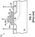
- FIG. 1Each memory cell 10 includes source and drain regions 14 / 16 formed in a semiconductor substrate 12 , with a channel region 18 there between.
- a floating gate 20is formed over and insulated from (and controls the conductivity of) a first portion of the channel region 18 , and over a portion of the drain region 16 .
- a control gate 22has a first portion 22 a that is disposed over and insulated from (and controls the conductivity of) a second portion of the channel region 18 , and a second portion 22 b that extends up and over the floating gate 20 .
- the floating gate 20 and control gate 22are insulated from the substrate 12 by a gate oxide 26 .
- the memory cellis referred to as split gate, because two different gates (floating gate 20 and control gate 22 ) separately control the conductivity of two different portions of the same channel region 18 . Therefore, the channel region 18 can conduct current between the source and drain regions 14 / 16 only if both of its portions are turned on by the floating and control gates 20 / 22 .
- the memory cellis erased (where electrons are removed from the floating gate) by placing a high positive voltage on the control gate 22 , which causes electrons on the floating gate 20 to tunnel through the intermediate insulation 24 from the floating gate 20 to the control gate 22 via the well-known technique of Fowler-Nordheim tunneling. Tunneling of electrons from one conductive gate to another conductive gate through intervening insulation is well known and not further described.
- the memory cellis programmed (where electrons are placed on the floating gate 20 ) by placing a positive voltage on the control gate 22 , and a positive voltage on the drain 16 .
- the portion of the channel region 18 under the control gate 22is turned on (made conductive) by the positive voltage on the control gate 22 .
- the portion of the channel region 18 under the floating gate 20is turned on (made conductive) by the positive voltages on the control gate 22 and drain region 16 being capacitively coupled to the floating gate 20 .
- Electron currentwill flow starting from the source 14 towards the drain 16 in the portion of the channel region 18 under the control gate 22 .
- the electronswill accelerate and become heated when they reach the gap between the control gate 22 and the floating gate 20 .
- Some of the heated electronswill be injected through the gate oxide 26 and onto the floating gate 20 due to the attractive electrostatic force from the floating gate 20 .
- This programming techniqueis well known as hot-electron injection, and is commonly used especially for split gate memory cells.
- the memory cell 10is read by placing positive read voltages on the drain region 16 and control gate 22 (which turns on the portion of channel region 18 under the control gate 22 ). If the floating gate 20 is positively charged (i.e. erased of electrons), then the portion of the channel region under the floating gate 20 is turned on as well (because of the capacitive coupling of the positive voltages to the floating gate 20 ), and current will flow across the channel region 18 , which is sensed as the erased or “1” state. If the floating gate 20 is negatively charged (i.e.
- the portion of the channel region under the floating gate 20is mostly or entirely turned off (because the capacitive coupling of the positive voltages cannot overcome the negative charge on the floating gate 20 ), and current will not flow (or there will be little flow) across the channel region 18 , which is sensed as the programmed or “0” state.
- source and draincan be interchangeable, where the floating gate 20 can extend partially over the source 14 instead of the drain 16 , as shown in FIG. 2 .
- split gate memory cells having more than two gatesare also known.
- U.S. Pat. No. 8,711,636(“the '636 patent”), incorporated herein by reference, discloses a split gate memory cell with an additional coupling gate disposed over and insulated from the source region, for better capacitive coupling to the floating gate. See for example FIG. 3 showing a split gate memory cell with a coupling gate 24 disposed over source region 14 .
- a split gate memory cell having four gatesis disclosed in U.S. Pat. Nos. 6,747,310 and 7,868,375, which are incorporated herein by reference.
- the four gate memory cell 10has a source region 14 , a drain region 16 , a floating gate 20 over a first portion of channel region 18 , a select gate 28 over a second portion of the channel region 18 (also referred to as the word line gate), a control gate 22 over the floating gate 20 , and an erase gate 30 over the source region 14 .
- Erasingis shown in FIG. 4 by electrons tunneling from the floating gate 20 to the erase gate 30 by placing a high positive voltage on the erase gate 30 .
- Programmingis shown in FIG. 4 by heated electrons from the channel region 18 injecting themselves onto the floating gate 20 by hot-electron injection.
- Table 1are exemplary voltages and current that can be used to program the memory cells:
- hot-electron injection programmingrequires a significant amount of electrical current for each memory cell to implement.
- programmingis often byte-by-byte, which means the memory device must include voltage and current sources sufficiently large enough to provide the necessary voltages and currents for concurrent programming of multiple memory cells.
- Mass programming using one or more internal charge pumpsis difficult because of the high programming current requirements of hot-electron injection.
- Some parallelization in programmingcan be achieved using external voltage source(s).
- mass programmingis simply not effective for most applications given the high current required, in additional to other factors such as the source line voltage drop.
- hot-electron injection programmingAnother issue with hot-electron injection programming is that it takes a relatively long time to complete, given that only some of the electrons traveling from the drain region 16 to the source region 14 end up being injected onto the floating gate 20 . The rest complete their journey to the source region 14 without being injected onto the floating gate 20 . Therefore, its efficiency in that respect is relatively low.
- a memory devicethat includes a semiconductor substrate, a memory cell and control circuitry.
- the memory cellincludes a source region and a drain region formed in the substrate, with a channel region of the substrate extending between the source and drain regions, a floating gate disposed over and insulated from a first portion of the channel region, for controlling a conductivity of the first portion of the channel region, a select gate disposed over and insulated from a second portion of the channel region, for controlling a conductivity of a second portion of the channel region, a control gate disposed over and insulated from the floating gate, and an erase gate disposed over and insulated from the source region, and disposed adjacent to and insulated from the floating gate.
- the control circuitryis configured to perform a program operation by applying a negative voltage to the erase gate for causing electrons to tunnel from the erase gate to the floating gate, and perform an erase operation by applying a positive voltage to the erase gate for causing electrons to tunnel from the floating gate to the erase gate.
- the methodincludes performing a program operation by applying a negative voltage to the erase gate to cause electrons to tunnel from the erase gate to the floating gate, and performing an erase operation by applying a positive voltage to the erase gate to cause electrons to tunnel from the floating gate to the erase gate.
- FIG. 1is a cross sectional view of a first embodiment of a conventional two-gate memory cell.
- FIG. 2is a cross sectional view of a second embodiment of a conventional two-gate memory cell.
- FIG. 3is a cross sectional view of a conventional three-gate memory cell.
- FIG. 4is a cross sectional view of a conventional four-gate memory cell.
- FIG. 5is a cross sectional view of a four-gate memory cell utilizing erase gate programming.
- FIG. 6is a plan view showing the architecture of an exemplary memory device of the present invention.
- a memory cell 32is shown in FIG. 5 , and includes a source region 36 and a drain region 38 formed in a semiconductor substrate 34 , with a channel region 40 of the substrate 34 extending between the source and drain regions 36 / 38 .
- a floating gate 42is disposed over and insulated from a first portion of channel region 40 .
- a select gate 44(also referred to as the word line gate) is disposed over and insulated from a second portion of the channel region 40 .
- a control gate 46is disposed over and insulated from the floating gate 42 .
- An erase gate 48is disposed over and insulated from the source region 36 , and disposed adjacent to and insulated from the floating gate 42 .
- the memory cell 32is a split gate memory cell because two different gates (floating gate 42 and select gate 44 ) separately control the conductivity of two different portions of the same channel region 40 .
- the memory cellsare preferably formed in pairs, where two adjacent memory cells share the same erase gate 48 and source region 36 , as shown in FIG. 5 . Two adjacent memory cell pairs can share the same drain region 38 .
- Table 2 belowillustrates the voltages applied to program the floating gate 42 with electrons.
- the programming of the floating gate 42 using the erase gate 48is highly efficient, as virtually all of the electrons in the electrical current generated by the negative voltage on the erase gate 48 will reach the floating gate 42 . Therefore, the electrical current needed to program the split gate memory cell using this erase gate programming technique is much lower than is needed using the hot-electron injection technique. This allows for more split gate memory cells to be programmed simultaneously without requiring larger and more powerful voltage and current sources that would otherwise be required, thus reducing the cost and size of the memory device. This programming technique is also faster than the prior art hot-electron injection programming technique of programming split gate memory cells. It is also ideal for those applications for which deep programming of the floating gate 42 of the split gate memory cell 32 is desired (i.e., placing a relatively high number of electrons on the floating gate 42 ).
- Memory cell 32is erased as described above, namely, applying a sufficiently high positive voltage on the erase gate 48 , such as positive 10-12 volts, causing electrons on the floating gate 42 to tunnel through the intervening insulation and onto the erase gate 48 .
- a sufficiently high positive voltageis applied to the select gate 44 , drain region 38 , source region 36 and control gate 46 during the erase operation.
- a lower positive voltagecan be used on the erase gate 48 to induce such erase tunneling if a negative voltage is also applied to the control gate 46 during the erase operation.
- a voltage of positive 6-8 volts on the erase gate 48 and a negative voltage of ⁇ 6 to ⁇ 8 volts on the control gate 46can be used to erase the floating gate 42 .
- Table 3illustrates the voltages applied to program the floating gate 42 with electrons in an alternate embodiment. Specifically, a positive voltage is applied to the control gate 46 simultaneously with the negative voltage on the erase gate 48 .
- the architecture of an exemplary memory device with the memory cells 32is illustrated in FIG. 6 .
- the memory deviceincludes an array 60 of the non-volatile memory cells 32 , which can be segregated into two separate planes (Plane A 62 a and Plane B 62 b ).
- the memory cells 32are preferably formed on a single chip, arranged in a plurality of rows and columns in the semiconductor substrate 34 . Adjacent to the array of non-volatile memory cells are address decoders (e.g.
- XDEC 64(a row decoder that drives the word lines), SLDRV 66 (a source line driver for driving the source lines), YMUX 68 (a column decoder that drives the bit lines), HVDEC 70 (a high voltage decoder) and a bit line controller (BLINHCTL 72 ), which are used to decode addresses and supply the various voltages to the various memory cell gates and regions during read, program, and erase operations for selected memory cells.
- Controller 76(containing control circuitry) controls the various device elements to implement each operation (program, erase, read) on target memory cells 32 (i.e., to directly or indirectly provide the voltages and currents to operate the memory cells 32 , including the voltages used to program the floating gate 42 using the erase gate negative voltage discussed above).
- Charge pump CHRGPMP 74provides the various voltages used to read, program and erase the memory cells under the control of the controller 76 .
- adjacentincludes “directly adjacent” (no intermediate materials, elements or space disposed there between) and “indirectly adjacent” (intermediate materials, elements or space disposed there between)
- mounted toincludes “directly mounted to” (no intermediate materials, elements or space disposed there between) and “indirectly mounted to” (intermediate materials, elements or spaced disposed there between)
- electrically coupledincludes “directly electrically coupled to” (no intermediate materials or elements there between that electrically connect the elements together) and “indirectly electrically coupled to” (intermediate materials or elements there between that electrically connect the elements together).
- forming an element “over a substrate”can include forming the element directly on the substrate with no intermediate materials/elements there between, as well as forming the element indirectly on the substrate with one or more intermediate materials/elements there between.
Landscapes
- Engineering & Computer Science (AREA)
- Microelectronics & Electronic Packaging (AREA)
- Non-Volatile Memory (AREA)
- Semiconductor Memories (AREA)
- Read Only Memory (AREA)
Abstract
Description
- This application claims the benefit of U.S. Provisional Application No. 62/722,107, filed on Aug. 23, 2018, and which is incorporated herein by reference.
- The present invention relates to non-volatile memory arrays.
- Split gate non-volatile memory cells, and arrays of such cells, are well known. For example, U.S. Pat. No. 5,029,130 (“the '130 patent”) discloses an array of split gate non-volatile memory cells, and is incorporated herein by reference for all purposes. The memory cell is shown in
FIG. 1 . Eachmemory cell 10 includes source anddrain regions 14/16 formed in asemiconductor substrate 12, with achannel region 18 there between. Afloating gate 20 is formed over and insulated from (and controls the conductivity of) a first portion of thechannel region 18, and over a portion of thedrain region 16. Acontrol gate 22 has afirst portion 22athat is disposed over and insulated from (and controls the conductivity of) a second portion of thechannel region 18, and asecond portion 22bthat extends up and over thefloating gate 20. Thefloating gate 20 andcontrol gate 22 are insulated from thesubstrate 12 by agate oxide 26. The memory cell is referred to as split gate, because two different gates (floatinggate 20 and control gate22) separately control the conductivity of two different portions of thesame channel region 18. Therefore, thechannel region 18 can conduct current between the source anddrain regions 14/16 only if both of its portions are turned on by the floating andcontrol gates 20/22. - The memory cell is erased (where electrons are removed from the floating gate) by placing a high positive voltage on the
control gate 22, which causes electrons on thefloating gate 20 to tunnel through theintermediate insulation 24 from thefloating gate 20 to thecontrol gate 22 via the well-known technique of Fowler-Nordheim tunneling. Tunneling of electrons from one conductive gate to another conductive gate through intervening insulation is well known and not further described. - The memory cell is programmed (where electrons are placed on the floating gate20) by placing a positive voltage on the
control gate 22, and a positive voltage on thedrain 16. The portion of thechannel region 18 under thecontrol gate 22 is turned on (made conductive) by the positive voltage on thecontrol gate 22. The portion of thechannel region 18 under thefloating gate 20 is turned on (made conductive) by the positive voltages on thecontrol gate 22 anddrain region 16 being capacitively coupled to thefloating gate 20. Electron current will flow starting from thesource 14 towards thedrain 16 in the portion of thechannel region 18 under thecontrol gate 22. The electrons will accelerate and become heated when they reach the gap between thecontrol gate 22 and thefloating gate 20. Some of the heated electrons will be injected through thegate oxide 26 and onto thefloating gate 20 due to the attractive electrostatic force from thefloating gate 20. This programming technique is well known as hot-electron injection, and is commonly used especially for split gate memory cells. - The
memory cell 10 is read by placing positive read voltages on thedrain region 16 and control gate22 (which turns on the portion ofchannel region 18 under the control gate22). If thefloating gate 20 is positively charged (i.e. erased of electrons), then the portion of the channel region under thefloating gate 20 is turned on as well (because of the capacitive coupling of the positive voltages to the floating gate20), and current will flow across thechannel region 18, which is sensed as the erased or “1” state. If thefloating gate 20 is negatively charged (i.e. programmed with electrons), then the portion of the channel region under thefloating gate 20 is mostly or entirely turned off (because the capacitive coupling of the positive voltages cannot overcome the negative charge on the floating gate20), and current will not flow (or there will be little flow) across thechannel region 18, which is sensed as the programmed or “0” state. Those skilled in the art understand that the terms source and drain can be interchangeable, where thefloating gate 20 can extend partially over thesource 14 instead of thedrain 16, as shown inFIG. 2 . - Split gate memory cells having more than two gates are also known. For example, U.S. Pat. No. 8,711,636 (“the '636 patent”), incorporated herein by reference, discloses a split gate memory cell with an additional coupling gate disposed over and insulated from the source region, for better capacitive coupling to the floating gate. See for example
FIG. 3 showing a split gate memory cell with acoupling gate 24 disposed oversource region 14. - A split gate memory cell having four gates is disclosed in U.S. Pat. Nos. 6,747,310 and 7,868,375, which are incorporated herein by reference. For example, as shown in
FIG. 4 , the fourgate memory cell 10 has asource region 14, adrain region 16, afloating gate 20 over a first portion ofchannel region 18, aselect gate 28 over a second portion of the channel region18 (also referred to as the word line gate), acontrol gate 22 over thefloating gate 20, and anerase gate 30 over thesource region 14. Erasing is shown inFIG. 4 by electrons tunneling from thefloating gate 20 to theerase gate 30 by placing a high positive voltage on theerase gate 30. Programming is shown inFIG. 4 by heated electrons from thechannel region 18 injecting themselves onto thefloating gate 20 by hot-electron injection. Below in Table 1 are exemplary voltages and current that can be used to program the memory cells: TABLE 1 SG 28Drain 16Source 14EG 30 CG 22 Program 1 V ~1 μA 4.5 V 4.5 V 10.5 V - One issue with hot-electron injection programming is that it requires a significant amount of electrical current for each memory cell to implement. However, programming is often byte-by-byte, which means the memory device must include voltage and current sources sufficiently large enough to provide the necessary voltages and currents for concurrent programming of multiple memory cells. Mass programming using one or more internal charge pumps is difficult because of the high programming current requirements of hot-electron injection. Some parallelization in programming can be achieved using external voltage source(s). However, mass programming is simply not effective for most applications given the high current required, in additional to other factors such as the source line voltage drop. Another issue with hot-electron injection programming is that it takes a relatively long time to complete, given that only some of the electrons traveling from the
drain region 16 to thesource region 14 end up being injected onto thefloating gate 20. The rest complete their journey to thesource region 14 without being injected onto thefloating gate 20. Therefore, its efficiency in that respect is relatively low. - There is a need for a more efficient technique of programming split gate memory cells having four gates.
- The aforementioned problems and needs are addressed by a memory device that includes a semiconductor substrate, a memory cell and control circuitry. The memory cell includes a source region and a drain region formed in the substrate, with a channel region of the substrate extending between the source and drain regions, a floating gate disposed over and insulated from a first portion of the channel region, for controlling a conductivity of the first portion of the channel region, a select gate disposed over and insulated from a second portion of the channel region, for controlling a conductivity of a second portion of the channel region, a control gate disposed over and insulated from the floating gate, and an erase gate disposed over and insulated from the source region, and disposed adjacent to and insulated from the floating gate. The control circuitry is configured to perform a program operation by applying a negative voltage to the erase gate for causing electrons to tunnel from the erase gate to the floating gate, and perform an erase operation by applying a positive voltage to the erase gate for causing electrons to tunnel from the floating gate to the erase gate.
- A method of operating a memory device having a memory cell that includes a source region and a drain region formed in a semiconductor substrate, with a channel region of the substrate extending between the source and drain regions, a floating gate disposed over and insulated from a first portion of the channel region, for controlling a conductivity of the first portion of the channel region, a select gate disposed over and insulated from a second portion of the channel region, for controlling a conductivity of a second portion of the channel region, a control gate disposed over and insulated from the floating gate, and an erase gate disposed over and insulated from the source region, and disposed adjacent to and insulated from the floating gate. The method includes performing a program operation by applying a negative voltage to the erase gate to cause electrons to tunnel from the erase gate to the floating gate, and performing an erase operation by applying a positive voltage to the erase gate to cause electrons to tunnel from the floating gate to the erase gate.
- Other objects and features of the present invention will become apparent by a review of the specification, claims and appended figures.
FIG. 1 is a cross sectional view of a first embodiment of a conventional two-gate memory cell.FIG. 2 is a cross sectional view of a second embodiment of a conventional two-gate memory cell.FIG. 3 is a cross sectional view of a conventional three-gate memory cell.FIG. 4 is a cross sectional view of a conventional four-gate memory cell.FIG. 5 is a cross sectional view of a four-gate memory cell utilizing erase gate programming.FIG. 6 is a plan view showing the architecture of an exemplary memory device of the present invention.- The present invention involves a new technique for programming split gate memory cells having four gates. Specifically, a
memory cell 32 is shown inFIG. 5 , and includes asource region 36 and adrain region 38 formed in asemiconductor substrate 34, with achannel region 40 of thesubstrate 34 extending between the source anddrain regions 36/38. Afloating gate 42 is disposed over and insulated from a first portion ofchannel region 40. A select gate44 (also referred to as the word line gate) is disposed over and insulated from a second portion of thechannel region 40. Acontrol gate 46 is disposed over and insulated from the floatinggate 42. An erasegate 48 is disposed over and insulated from thesource region 36, and disposed adjacent to and insulated from the floatinggate 42. Thememory cell 32 is a split gate memory cell because two different gates (floatinggate 42 and select gate44) separately control the conductivity of two different portions of thesame channel region 40. The memory cells are preferably formed in pairs, where two adjacent memory cells share the same erasegate 48 andsource region 36, as shown inFIG. 5 . Two adjacent memory cell pairs can share thesame drain region 38. - Table 2 below illustrates the voltages applied to program the floating
gate 42 with electrons. TABLE 2 SG 44Drain 38Source 36EG 48CG 46Program 0 V 0 V 0 V −11 V to −13 V 0 V
By applying a negative voltage of sufficient magnitude to the erasegate 48, with a zero voltage (i.e., ground) applied to the remaining elements (selectgate 44,drain region 38,source region 36 and control gate46), electrons will tunnel from the erasegate 48 to the floatinggate 42, as graphically shown inFIG. 5 .- The programming of the floating
gate 42 using the erasegate 48 is highly efficient, as virtually all of the electrons in the electrical current generated by the negative voltage on the erasegate 48 will reach the floatinggate 42. Therefore, the electrical current needed to program the split gate memory cell using this erase gate programming technique is much lower than is needed using the hot-electron injection technique. This allows for more split gate memory cells to be programmed simultaneously without requiring larger and more powerful voltage and current sources that would otherwise be required, thus reducing the cost and size of the memory device. This programming technique is also faster than the prior art hot-electron injection programming technique of programming split gate memory cells. It is also ideal for those applications for which deep programming of the floatinggate 42 of the splitgate memory cell 32 is desired (i.e., placing a relatively high number of electrons on the floating gate42). Memory cell 32 is erased as described above, namely, applying a sufficiently high positive voltage on the erasegate 48, such as positive 10-12 volts, causing electrons on the floatinggate 42 to tunnel through the intervening insulation and onto the erasegate 48. Preferably, a zero voltage is applied to theselect gate 44,drain region 38,source region 36 andcontrol gate 46 during the erase operation. Alternately, a lower positive voltage can be used on the erasegate 48 to induce such erase tunneling if a negative voltage is also applied to thecontrol gate 46 during the erase operation. For example, a voltage of positive 6-8 volts on the erasegate 48 and a negative voltage of −6 to −8 volts on thecontrol gate 46 can be used to erase the floatinggate 42.- Table 3 below illustrates the voltages applied to program the floating
gate 42 with electrons in an alternate embodiment. Specifically, a positive voltage is applied to thecontrol gate 46 simultaneously with the negative voltage on the erasegate 48. TABLE 3 SG 44Drain 38Source 36EG 48CG 46Program 0 V 0 V 0 V −7 V to −9 V 7 V to 9 V
The positive voltage on thecontrol gate 46 couples to the floatinggate 42, thereby better attracting the electrons on the erasegate 48 to tunnel to the floatinggate 42. By applying a positive voltage on thecontrol gate 46, the magnitude of the negative voltage on the erasegate 48 can be reduced, thereby further reducing the size and cost of the negative voltage source used by the device.- The architecture of an exemplary memory device with the
memory cells 32 is illustrated inFIG. 6 . The memory device includes anarray 60 of thenon-volatile memory cells 32, which can be segregated into two separate planes (Plane A62aandPlane B 62b). Thememory cells 32 are preferably formed on a single chip, arranged in a plurality of rows and columns in thesemiconductor substrate 34. Adjacent to the array of non-volatile memory cells are address decoders (e.g. XDEC64 (a row decoder that drives the word lines), SLDRV66 (a source line driver for driving the source lines), YMUX68 (a column decoder that drives the bit lines), HVDEC70 (a high voltage decoder) and a bit line controller (BLINHCTL72), which are used to decode addresses and supply the various voltages to the various memory cell gates and regions during read, program, and erase operations for selected memory cells. Controller76 (containing control circuitry) controls the various device elements to implement each operation (program, erase, read) on target memory cells32 (i.e., to directly or indirectly provide the voltages and currents to operate thememory cells 32, including the voltages used to program the floatinggate 42 using the erase gate negative voltage discussed above).Charge pump CHRGPMP 74 provides the various voltages used to read, program and erase the memory cells under the control of thecontroller 76. - It is to be understood that the present invention is not limited to the embodiment(s) described above and illustrated herein, but encompasses any and all variations falling within the scope of any claims. For example, references to the present invention herein are not intended to limit the scope of any claim or claim term, but instead merely make reference to one or more features that may be covered by one or more of the claims. Materials, processes and numerical examples described above are exemplary only, and should not be deemed to limit the claims. Further, as is apparent from the claims and specification, not all method steps need be performed in the exact order illustrated or claimed, but rather in any order that allows the proper formation of the memory device of the present invention. Lastly, single layers of material could be formed as multiple layers of such or similar materials, and vice versa.
- It should be noted that, as used herein, the terms “over” and “on” both inclusively include “directly on” (no intermediate materials, elements or space disposed there between) and “indirectly on” (intermediate materials, elements or space disposed there between). Likewise, the term “adjacent” includes “directly adjacent” (no intermediate materials, elements or space disposed there between) and “indirectly adjacent” (intermediate materials, elements or space disposed there between), “mounted to” includes “directly mounted to” (no intermediate materials, elements or space disposed there between) and “indirectly mounted to” (intermediate materials, elements or spaced disposed there between), and “electrically coupled” includes “directly electrically coupled to” (no intermediate materials or elements there between that electrically connect the elements together) and “indirectly electrically coupled to” (intermediate materials or elements there between that electrically connect the elements together). For example, forming an element “over a substrate” can include forming the element directly on the substrate with no intermediate materials/elements there between, as well as forming the element indirectly on the substrate with one or more intermediate materials/elements there between.
Claims (18)
Priority Applications (7)
| Application Number | Priority Date | Filing Date | Title |
|---|---|---|---|
| US16/209,515US10714489B2 (en) | 2018-08-23 | 2018-12-04 | Method of programming a split-gate flash memory cell with erase gate |
| JP2021510104AJP7116844B2 (en) | 2018-08-23 | 2019-07-09 | Method for programming split-gate flash memory cells with erase gates |
| CN201980054482.XACN112585680B (en) | 2018-08-23 | 2019-07-09 | Method of programming split gate flash memory cells with erase gates |
| PCT/US2019/041080WO2020040894A1 (en) | 2018-08-23 | 2019-07-09 | Method of programming a split-gate flash memory cell with erase gate |
| EP19790338.8AEP3841581B1 (en) | 2018-08-23 | 2019-07-09 | Method of programming a split-gate flash memory cell with erase gate |
| KR1020217003797AKR102290104B1 (en) | 2018-08-23 | 2019-07-09 | How to Program a Removable Gate Flash Memory Cell With an Erase Gate |
| TW108128769ATWI757625B (en) | 2018-08-23 | 2019-08-13 | Method of programming a split-gate flash memory cell with erase gate |
Applications Claiming Priority (2)
| Application Number | Priority Date | Filing Date | Title |
|---|---|---|---|
| US201862722107P | 2018-08-23 | 2018-08-23 | |
| US16/209,515US10714489B2 (en) | 2018-08-23 | 2018-12-04 | Method of programming a split-gate flash memory cell with erase gate |
Publications (2)
| Publication Number | Publication Date |
|---|---|
| US20200066738A1true US20200066738A1 (en) | 2020-02-27 |
| US10714489B2 US10714489B2 (en) | 2020-07-14 |
Family
ID=69583741
Family Applications (1)
| Application Number | Title | Priority Date | Filing Date |
|---|---|---|---|
| US16/209,515ActiveUS10714489B2 (en) | 2018-08-23 | 2018-12-04 | Method of programming a split-gate flash memory cell with erase gate |
Country Status (7)
| Country | Link |
|---|---|
| US (1) | US10714489B2 (en) |
| EP (1) | EP3841581B1 (en) |
| JP (1) | JP7116844B2 (en) |
| KR (1) | KR102290104B1 (en) |
| CN (1) | CN112585680B (en) |
| TW (1) | TWI757625B (en) |
| WO (1) | WO2020040894A1 (en) |
Cited By (1)
| Publication number | Priority date | Publication date | Assignee | Title |
|---|---|---|---|---|
| US11955180B2 (en)* | 2020-12-29 | 2024-04-09 | Micron Technology, Inc. | Memories having split-gate memory cells |
Families Citing this family (2)
| Publication number | Priority date | Publication date | Assignee | Title |
|---|---|---|---|---|
| CN114335186B (en)* | 2020-09-30 | 2025-02-07 | 硅存储技术股份有限公司 | Split gate non-volatile memory cell with erase gate disposed above word line gate and method of making the same |
| CN114743976B (en)* | 2022-05-10 | 2025-09-23 | 杭州知存算力科技有限公司 | Semiconductor device and method for manufacturing the same |
Citations (1)
| Publication number | Priority date | Publication date | Assignee | Title |
|---|---|---|---|---|
| US20170110194A1 (en)* | 2015-10-19 | 2017-04-20 | Silicon Storage Technology, Inc. | Power Driven Optimization For Flash Memory |
Family Cites Families (11)
| Publication number | Priority date | Publication date | Assignee | Title |
|---|---|---|---|---|
| US5029130A (en) | 1990-01-22 | 1991-07-02 | Silicon Storage Technology, Inc. | Single transistor non-valatile electrically alterable semiconductor memory device |
| US5386132A (en) | 1992-11-02 | 1995-01-31 | Wong; Chun C. D. | Multimedia storage system with highly compact memory device |
| KR100232235B1 (en) | 1996-11-15 | 1999-12-01 | 김영환 | Nonvolatile memory device |
| JP4647175B2 (en) | 2002-04-18 | 2011-03-09 | ルネサスエレクトロニクス株式会社 | Semiconductor integrated circuit device |
| US6747310B2 (en) | 2002-10-07 | 2004-06-08 | Actrans System Inc. | Flash memory cells with separated self-aligned select and erase gates, and process of fabrication |
| US7315056B2 (en)* | 2004-06-07 | 2008-01-01 | Silicon Storage Technology, Inc. | Semiconductor memory array of floating gate memory cells with program/erase and select gates |
| US20090039410A1 (en) | 2007-08-06 | 2009-02-12 | Xian Liu | Split Gate Non-Volatile Flash Memory Cell Having A Floating Gate, Control Gate, Select Gate And An Erase Gate With An Overhang Over The Floating Gate, Array And Method Of Manufacturing |
| JP2009301703A (en) | 2009-09-24 | 2009-12-24 | Renesas Technology Corp | Semiconductor device |
| US8711636B2 (en) | 2011-05-13 | 2014-04-29 | Silicon Storage Technology, Inc. | Method of operating a split gate flash memory cell with coupling gate |
| US8576648B2 (en) | 2011-11-09 | 2013-11-05 | Silicon Storage Technology, Inc. | Method of testing data retention of a non-volatile memory cell having a floating gate |
| CN105609131A (en) | 2014-07-22 | 2016-05-25 | 硅存储技术公司 | System and method for inhibiting erasing of part of splitting gate flash memory unit sector |
- 2018
- 2018-12-04USUS16/209,515patent/US10714489B2/enactiveActive
- 2019
- 2019-07-09EPEP19790338.8Apatent/EP3841581B1/enactiveActive
- 2019-07-09KRKR1020217003797Apatent/KR102290104B1/enactiveActive
- 2019-07-09WOPCT/US2019/041080patent/WO2020040894A1/ennot_activeCeased
- 2019-07-09CNCN201980054482.XApatent/CN112585680B/enactiveActive
- 2019-07-09JPJP2021510104Apatent/JP7116844B2/enactiveActive
- 2019-08-13TWTW108128769Apatent/TWI757625B/enactive
Patent Citations (1)
| Publication number | Priority date | Publication date | Assignee | Title |
|---|---|---|---|---|
| US20170110194A1 (en)* | 2015-10-19 | 2017-04-20 | Silicon Storage Technology, Inc. | Power Driven Optimization For Flash Memory |
Cited By (1)
| Publication number | Priority date | Publication date | Assignee | Title |
|---|---|---|---|---|
| US11955180B2 (en)* | 2020-12-29 | 2024-04-09 | Micron Technology, Inc. | Memories having split-gate memory cells |
Also Published As
| Publication number | Publication date |
|---|---|
| TW202025160A (en) | 2020-07-01 |
| WO2020040894A1 (en) | 2020-02-27 |
| EP3841581A1 (en) | 2021-06-30 |
| KR20210019575A (en) | 2021-02-22 |
| JP2021535531A (en) | 2021-12-16 |
| JP7116844B2 (en) | 2022-08-10 |
| US10714489B2 (en) | 2020-07-14 |
| CN112585680A (en) | 2021-03-30 |
| KR102290104B1 (en) | 2021-08-17 |
| CN112585680B (en) | 2021-12-14 |
| EP3841581B1 (en) | 2022-06-15 |
| TWI757625B (en) | 2022-03-11 |
Similar Documents
| Publication | Publication Date | Title |
|---|---|---|
| US10388389B2 (en) | Flash memory array with individual memory cell read, program and erase | |
| US10460811B2 (en) | Array of three-gate flash memory cells with individual memory cell read, program and erase | |
| EP4046158B1 (en) | Four gate, split-gate flash memory array with byte erase operation | |
| US10607703B2 (en) | Split-gate flash memory array with byte erase operation | |
| US10838652B2 (en) | Programming of memory cell having gate capacitively coupled to floating gate | |
| US10714489B2 (en) | Method of programming a split-gate flash memory cell with erase gate | |
| CN109328385B (en) | Memory cell array with individual memory cell reading, programming and erasing |
Legal Events
| Date | Code | Title | Description |
|---|---|---|---|
| FEPP | Fee payment procedure | Free format text:ENTITY STATUS SET TO UNDISCOUNTED (ORIGINAL EVENT CODE: BIG.); ENTITY STATUS OF PATENT OWNER: LARGE ENTITY | |
| AS | Assignment | Owner name:SILICON STORAGE TECHNOLOGY, INC., CALIFORNIA Free format text:ASSIGNMENT OF ASSIGNORS INTEREST;ASSIGNORS:TKACHEV, YURI;KOTOV, ALEXANDER;DO, NHAN;REEL/FRAME:047884/0052 Effective date:20181212 | |
| STPP | Information on status: patent application and granting procedure in general | Free format text:RESPONSE TO NON-FINAL OFFICE ACTION ENTERED AND FORWARDED TO EXAMINER | |
| STPP | Information on status: patent application and granting procedure in general | Free format text:NOTICE OF ALLOWANCE MAILED -- APPLICATION RECEIVED IN OFFICE OF PUBLICATIONS | |
| AS | Assignment | Owner name:JPMORGAN CHASE BANK, N.A., AS ADMINISTRATIVE AGENT, DELAWARE Free format text:SECURITY INTEREST;ASSIGNORS:MICROCHIP TECHNOLOGY INC.;SILICON STORAGE TECHNOLOGY, INC.;ATMEL CORPORATION;AND OTHERS;REEL/FRAME:053311/0305 Effective date:20200327 | |
| AS | Assignment | Owner name:ATMEL CORPORATION, ARIZONA Free format text:RELEASE BY SECURED PARTY;ASSIGNOR:JPMORGAN CHASE BANK, N.A, AS ADMINISTRATIVE AGENT;REEL/FRAME:053466/0011 Effective date:20200529 Owner name:MICROSEMI CORPORATION, CALIFORNIA Free format text:RELEASE BY SECURED PARTY;ASSIGNOR:JPMORGAN CHASE BANK, N.A, AS ADMINISTRATIVE AGENT;REEL/FRAME:053466/0011 Effective date:20200529 Owner name:SILICON STORAGE TECHNOLOGY, INC., ARIZONA Free format text:RELEASE BY SECURED PARTY;ASSIGNOR:JPMORGAN CHASE BANK, N.A, AS ADMINISTRATIVE AGENT;REEL/FRAME:053466/0011 Effective date:20200529 Owner name:MICROSEMI STORAGE SOLUTIONS, INC., ARIZONA Free format text:RELEASE BY SECURED PARTY;ASSIGNOR:JPMORGAN CHASE BANK, N.A, AS ADMINISTRATIVE AGENT;REEL/FRAME:053466/0011 Effective date:20200529 Owner name:MICROCHIP TECHNOLOGY INC., ARIZONA Free format text:RELEASE BY SECURED PARTY;ASSIGNOR:JPMORGAN CHASE BANK, N.A, AS ADMINISTRATIVE AGENT;REEL/FRAME:053466/0011 Effective date:20200529 | |
| AS | Assignment | Owner name:JPMORGAN CHASE BANK, N.A., AS ADMINISTRATIVE AGENT, ILLINOIS Free format text:SECURITY INTEREST;ASSIGNORS:MICROCHIP TECHNOLOGY INC.;SILICON STORAGE TECHNOLOGY, INC.;ATMEL CORPORATION;AND OTHERS;REEL/FRAME:052856/0909 Effective date:20200529 Owner name:WELLS FARGO BANK, NATIONAL ASSOCIATION, MINNESOTA Free format text:SECURITY INTEREST;ASSIGNORS:MICROCHIP TECHNOLOGY INC.;SILICON STORAGE TECHNOLOGY, INC.;ATMEL CORPORATION;AND OTHERS;REEL/FRAME:053468/0705 Effective date:20200529 | |
| STPP | Information on status: patent application and granting procedure in general | Free format text:PUBLICATIONS -- ISSUE FEE PAYMENT VERIFIED | |
| STCF | Information on status: patent grant | Free format text:PATENTED CASE | |
| AS | Assignment | Owner name:WELLS FARGO BANK, NATIONAL ASSOCIATION, AS COLLATERAL AGENT, MINNESOTA Free format text:SECURITY INTEREST;ASSIGNORS:MICROCHIP TECHNOLOGY INCORPORATED;SILICON STORAGE TECHNOLOGY, INC.;ATMEL CORPORATION;AND OTHERS;REEL/FRAME:055671/0612 Effective date:20201217 | |
| AS | Assignment | Owner name:WELLS FARGO BANK, NATIONAL ASSOCIATION, AS NOTES COLLATERAL AGENT, MINNESOTA Free format text:SECURITY INTEREST;ASSIGNORS:MICROCHIP TECHNOLOGY INCORPORATED;SILICON STORAGE TECHNOLOGY, INC.;ATMEL CORPORATION;AND OTHERS;REEL/FRAME:057935/0474 Effective date:20210528 | |
| AS | Assignment | Owner name:WELLS FARGO BANK, NATIONAL ASSOCIATION, AS NOTES COLLATERAL AGENT, MINNESOTA Free format text:GRANT OF SECURITY INTEREST IN PATENT RIGHTS;ASSIGNORS:MICROCHIP TECHNOLOGY INCORPORATED;SILICON STORAGE TECHNOLOGY, INC.;ATMEL CORPORATION;AND OTHERS;REEL/FRAME:058214/0625 Effective date:20211117 Owner name:JPMORGAN CHASE BANK, N.A., AS ADMINISTRATIVE AGENT, ILLINOIS Free format text:GRANT OF SECURITY INTEREST IN PATENT RIGHTS;ASSIGNORS:MICROCHIP TECHNOLOGY INCORPORATED;SILICON STORAGE TECHNOLOGY, INC.;ATMEL CORPORATION;AND OTHERS;REEL/FRAME:058214/0380 Effective date:20211117 Owner name:WELLS FARGO BANK, NATIONAL ASSOCIATION, AS NOTES COLLATERAL AGENT, MINNESOTA Free format text:GRANT OF SECURITY INTEREST IN PATENT RIGHTS;ASSIGNORS:MICROCHIP TECHNOLOGY INCORPORATED;SILICON STORAGE TECHNOLOGY, INC.;ATMEL CORPORATION;AND OTHERS;REEL/FRAME:058214/0238 Effective date:20211117 | |
| AS | Assignment | Owner name:MICROSEMI STORAGE SOLUTIONS, INC., ARIZONA Free format text:RELEASE BY SECURED PARTY;ASSIGNOR:JPMORGAN CHASE BANK, N.A., AS ADMINISTRATIVE AGENT;REEL/FRAME:059264/0384 Effective date:20220218 Owner name:MICROSEMI CORPORATION, ARIZONA Free format text:RELEASE BY SECURED PARTY;ASSIGNOR:JPMORGAN CHASE BANK, N.A., AS ADMINISTRATIVE AGENT;REEL/FRAME:059264/0384 Effective date:20220218 Owner name:ATMEL CORPORATION, ARIZONA Free format text:RELEASE BY SECURED PARTY;ASSIGNOR:JPMORGAN CHASE BANK, N.A., AS ADMINISTRATIVE AGENT;REEL/FRAME:059264/0384 Effective date:20220218 Owner name:SILICON STORAGE TECHNOLOGY, INC., ARIZONA Free format text:RELEASE BY SECURED PARTY;ASSIGNOR:JPMORGAN CHASE BANK, N.A., AS ADMINISTRATIVE AGENT;REEL/FRAME:059264/0384 Effective date:20220218 Owner name:MICROCHIP TECHNOLOGY INCORPORATED, ARIZONA Free format text:RELEASE BY SECURED PARTY;ASSIGNOR:JPMORGAN CHASE BANK, N.A., AS ADMINISTRATIVE AGENT;REEL/FRAME:059264/0384 Effective date:20220218 Owner name:MICROSEMI STORAGE SOLUTIONS, INC., ARIZONA Free format text:RELEASE BY SECURED PARTY;ASSIGNOR:JPMORGAN CHASE BANK, N.A., AS ADMINISTRATIVE AGENT;REEL/FRAME:059263/0001 Effective date:20220218 Owner name:MICROSEMI CORPORATION, ARIZONA Free format text:RELEASE BY SECURED PARTY;ASSIGNOR:JPMORGAN CHASE BANK, N.A., AS ADMINISTRATIVE AGENT;REEL/FRAME:059263/0001 Effective date:20220218 Owner name:ATMEL CORPORATION, ARIZONA Free format text:RELEASE BY SECURED PARTY;ASSIGNOR:JPMORGAN CHASE BANK, N.A., AS ADMINISTRATIVE AGENT;REEL/FRAME:059263/0001 Effective date:20220218 Owner name:SILICON STORAGE TECHNOLOGY, INC., ARIZONA Free format text:RELEASE BY SECURED PARTY;ASSIGNOR:JPMORGAN CHASE BANK, N.A., AS ADMINISTRATIVE AGENT;REEL/FRAME:059263/0001 Effective date:20220218 Owner name:MICROCHIP TECHNOLOGY INCORPORATED, ARIZONA Free format text:RELEASE BY SECURED PARTY;ASSIGNOR:JPMORGAN CHASE BANK, N.A., AS ADMINISTRATIVE AGENT;REEL/FRAME:059263/0001 Effective date:20220218 | |
| AS | Assignment | Owner name:MICROSEMI STORAGE SOLUTIONS, INC., ARIZONA Free format text:RELEASE BY SECURED PARTY;ASSIGNOR:WELLS FARGO BANK, NATIONAL ASSOCIATION, AS NOTES COLLATERAL AGENT;REEL/FRAME:059357/0823 Effective date:20220228 Owner name:MICROSEMI CORPORATION, ARIZONA Free format text:RELEASE BY SECURED PARTY;ASSIGNOR:WELLS FARGO BANK, NATIONAL ASSOCIATION, AS NOTES COLLATERAL AGENT;REEL/FRAME:059357/0823 Effective date:20220228 Owner name:ATMEL CORPORATION, ARIZONA Free format text:RELEASE BY SECURED PARTY;ASSIGNOR:WELLS FARGO BANK, NATIONAL ASSOCIATION, AS NOTES COLLATERAL AGENT;REEL/FRAME:059357/0823 Effective date:20220228 Owner name:SILICON STORAGE TECHNOLOGY, INC., ARIZONA Free format text:RELEASE BY SECURED PARTY;ASSIGNOR:WELLS FARGO BANK, NATIONAL ASSOCIATION, AS NOTES COLLATERAL AGENT;REEL/FRAME:059357/0823 Effective date:20220228 Owner name:MICROCHIP TECHNOLOGY INCORPORATED, ARIZONA Free format text:RELEASE BY SECURED PARTY;ASSIGNOR:WELLS FARGO BANK, NATIONAL ASSOCIATION, AS NOTES COLLATERAL AGENT;REEL/FRAME:059357/0823 Effective date:20220228 Owner name:MICROSEMI STORAGE SOLUTIONS, INC., ARIZONA Free format text:RELEASE BY SECURED PARTY;ASSIGNOR:WELLS FARGO BANK, NATIONAL ASSOCIATION, AS NOTES COLLATERAL AGENT;REEL/FRAME:059358/0335 Effective date:20220228 Owner name:MICROSEMI CORPORATION, ARIZONA Free format text:RELEASE BY SECURED PARTY;ASSIGNOR:WELLS FARGO BANK, NATIONAL ASSOCIATION, AS NOTES COLLATERAL AGENT;REEL/FRAME:059358/0335 Effective date:20220228 Owner name:ATMEL CORPORATION, ARIZONA Free format text:RELEASE BY SECURED PARTY;ASSIGNOR:WELLS FARGO BANK, NATIONAL ASSOCIATION, AS NOTES COLLATERAL AGENT;REEL/FRAME:059358/0335 Effective date:20220228 Owner name:SILICON STORAGE TECHNOLOGY, INC., ARIZONA Free format text:RELEASE BY SECURED PARTY;ASSIGNOR:WELLS FARGO BANK, NATIONAL ASSOCIATION, AS NOTES COLLATERAL AGENT;REEL/FRAME:059358/0335 Effective date:20220228 Owner name:MICROCHIP TECHNOLOGY INCORPORATED, ARIZONA Free format text:RELEASE BY SECURED PARTY;ASSIGNOR:WELLS FARGO BANK, NATIONAL ASSOCIATION, AS NOTES COLLATERAL AGENT;REEL/FRAME:059358/0335 Effective date:20220228 | |
| AS | Assignment | Owner name:MICROSEMI STORAGE SOLUTIONS, INC., ARIZONA Free format text:RELEASE BY SECURED PARTY;ASSIGNOR:WELLS FARGO BANK, NATIONAL ASSOCIATION, AS NOTES COLLATERAL AGENT;REEL/FRAME:059863/0400 Effective date:20220228 Owner name:MICROSEMI CORPORATION, ARIZONA Free format text:RELEASE BY SECURED PARTY;ASSIGNOR:WELLS FARGO BANK, NATIONAL ASSOCIATION, AS NOTES COLLATERAL AGENT;REEL/FRAME:059863/0400 Effective date:20220228 Owner name:ATMEL CORPORATION, ARIZONA Free format text:RELEASE BY SECURED PARTY;ASSIGNOR:WELLS FARGO BANK, NATIONAL ASSOCIATION, AS NOTES COLLATERAL AGENT;REEL/FRAME:059863/0400 Effective date:20220228 Owner name:SILICON STORAGE TECHNOLOGY, INC., ARIZONA Free format text:RELEASE BY SECURED PARTY;ASSIGNOR:WELLS FARGO BANK, NATIONAL ASSOCIATION, AS NOTES COLLATERAL AGENT;REEL/FRAME:059863/0400 Effective date:20220228 Owner name:MICROCHIP TECHNOLOGY INCORPORATED, ARIZONA Free format text:RELEASE BY SECURED PARTY;ASSIGNOR:WELLS FARGO BANK, NATIONAL ASSOCIATION, AS NOTES COLLATERAL AGENT;REEL/FRAME:059863/0400 Effective date:20220228 | |
| AS | Assignment | Owner name:MICROSEMI STORAGE SOLUTIONS, INC., ARIZONA Free format text:RELEASE BY SECURED PARTY;ASSIGNOR:WELLS FARGO BANK, NATIONAL ASSOCIATION, AS NOTES COLLATERAL AGENT;REEL/FRAME:060894/0437 Effective date:20220228 Owner name:MICROSEMI CORPORATION, ARIZONA Free format text:RELEASE BY SECURED PARTY;ASSIGNOR:WELLS FARGO BANK, NATIONAL ASSOCIATION, AS NOTES COLLATERAL AGENT;REEL/FRAME:060894/0437 Effective date:20220228 Owner name:ATMEL CORPORATION, ARIZONA Free format text:RELEASE BY SECURED PARTY;ASSIGNOR:WELLS FARGO BANK, NATIONAL ASSOCIATION, AS NOTES COLLATERAL AGENT;REEL/FRAME:060894/0437 Effective date:20220228 Owner name:SILICON STORAGE TECHNOLOGY, INC., ARIZONA Free format text:RELEASE BY SECURED PARTY;ASSIGNOR:WELLS FARGO BANK, NATIONAL ASSOCIATION, AS NOTES COLLATERAL AGENT;REEL/FRAME:060894/0437 Effective date:20220228 Owner name:MICROCHIP TECHNOLOGY INCORPORATED, ARIZONA Free format text:RELEASE BY SECURED PARTY;ASSIGNOR:WELLS FARGO BANK, NATIONAL ASSOCIATION, AS NOTES COLLATERAL AGENT;REEL/FRAME:060894/0437 Effective date:20220228 | |
| MAFP | Maintenance fee payment | Free format text:PAYMENT OF MAINTENANCE FEE, 4TH YEAR, LARGE ENTITY (ORIGINAL EVENT CODE: M1551); ENTITY STATUS OF PATENT OWNER: LARGE ENTITY Year of fee payment:4 |