US20200026002A1 - Compact and low loss y-junction for submicron silicon waveguide - Google Patents
Compact and low loss y-junction for submicron silicon waveguideDownload PDFInfo
- Publication number
- US20200026002A1 US20200026002A1US16/214,365US201816214365AUS2020026002A1US 20200026002 A1US20200026002 A1US 20200026002A1US 201816214365 AUS201816214365 AUS 201816214365AUS 2020026002 A1US2020026002 A1US 2020026002A1
- Authority
- US
- United States
- Prior art keywords
- width
- tapered section
- output ports
- input port
- maximum width
- Prior art date
- Legal status (The legal status is an assumption and is not a legal conclusion. Google has not performed a legal analysis and makes no representation as to the accuracy of the status listed.)
- Granted
Links
Images


Classifications
- G—PHYSICS
- G02—OPTICS
- G02B—OPTICAL ELEMENTS, SYSTEMS OR APPARATUS
- G02B6/00—Light guides; Structural details of arrangements comprising light guides and other optical elements, e.g. couplings
- G02B6/10—Light guides; Structural details of arrangements comprising light guides and other optical elements, e.g. couplings of the optical waveguide type
- G02B6/12—Light guides; Structural details of arrangements comprising light guides and other optical elements, e.g. couplings of the optical waveguide type of the integrated circuit kind
- G02B6/122—Basic optical elements, e.g. light-guiding paths
- G02B6/125—Bends, branchings or intersections
- G—PHYSICS
- G02—OPTICS
- G02B—OPTICAL ELEMENTS, SYSTEMS OR APPARATUS
- G02B27/00—Optical systems or apparatus not provided for by any of the groups G02B1/00 - G02B26/00, G02B30/00
- G02B27/0012—Optical design, e.g. procedures, algorithms, optimisation routines
- G—PHYSICS
- G02—OPTICS
- G02B—OPTICAL ELEMENTS, SYSTEMS OR APPARATUS
- G02B6/00—Light guides; Structural details of arrangements comprising light guides and other optical elements, e.g. couplings
- G02B6/10—Light guides; Structural details of arrangements comprising light guides and other optical elements, e.g. couplings of the optical waveguide type
- G02B6/107—Subwavelength-diameter waveguides, e.g. nanowires
- G—PHYSICS
- G02—OPTICS
- G02B—OPTICAL ELEMENTS, SYSTEMS OR APPARATUS
- G02B6/00—Light guides; Structural details of arrangements comprising light guides and other optical elements, e.g. couplings
- G02B6/10—Light guides; Structural details of arrangements comprising light guides and other optical elements, e.g. couplings of the optical waveguide type
- G02B6/12—Light guides; Structural details of arrangements comprising light guides and other optical elements, e.g. couplings of the optical waveguide type of the integrated circuit kind
- G02B6/122—Basic optical elements, e.g. light-guiding paths
- G02B6/1228—Tapered waveguides, e.g. integrated spot-size transformers
- G—PHYSICS
- G02—OPTICS
- G02B—OPTICAL ELEMENTS, SYSTEMS OR APPARATUS
- G02B6/00—Light guides; Structural details of arrangements comprising light guides and other optical elements, e.g. couplings
- G02B6/24—Coupling light guides
- G02B6/26—Optical coupling means
- G02B6/28—Optical coupling means having data bus means, i.e. plural waveguides interconnected and providing an inherently bidirectional system by mixing and splitting signals
- G02B6/2804—Optical coupling means having data bus means, i.e. plural waveguides interconnected and providing an inherently bidirectional system by mixing and splitting signals forming multipart couplers without wavelength selective elements, e.g. "T" couplers, star couplers
- G02B6/2808—Optical coupling means having data bus means, i.e. plural waveguides interconnected and providing an inherently bidirectional system by mixing and splitting signals forming multipart couplers without wavelength selective elements, e.g. "T" couplers, star couplers using a mixing element which evenly distributes an input signal over a number of outputs
- G06F17/5009—
- G06F17/5018—
- G06F17/5077—
- G—PHYSICS
- G06—COMPUTING OR CALCULATING; COUNTING
- G06F—ELECTRIC DIGITAL DATA PROCESSING
- G06F30/00—Computer-aided design [CAD]
- G06F30/20—Design optimisation, verification or simulation
- G—PHYSICS
- G06—COMPUTING OR CALCULATING; COUNTING
- G06F—ELECTRIC DIGITAL DATA PROCESSING
- G06F30/00—Computer-aided design [CAD]
- G06F30/20—Design optimisation, verification or simulation
- G06F30/23—Design optimisation, verification or simulation using finite element methods [FEM] or finite difference methods [FDM]
- G—PHYSICS
- G06—COMPUTING OR CALCULATING; COUNTING
- G06F—ELECTRIC DIGITAL DATA PROCESSING
- G06F30/00—Computer-aided design [CAD]
- G06F30/30—Circuit design
- G06F30/39—Circuit design at the physical level
- G06F30/394—Routing
- G—PHYSICS
- G06—COMPUTING OR CALCULATING; COUNTING
- G06N—COMPUTING ARRANGEMENTS BASED ON SPECIFIC COMPUTATIONAL MODELS
- G06N3/00—Computing arrangements based on biological models
- G06N3/12—Computing arrangements based on biological models using genetic models
- G06N3/126—Evolutionary algorithms, e.g. genetic algorithms or genetic programming
- G—PHYSICS
- G02—OPTICS
- G02B—OPTICAL ELEMENTS, SYSTEMS OR APPARATUS
- G02B6/00—Light guides; Structural details of arrangements comprising light guides and other optical elements, e.g. couplings
- G02B6/10—Light guides; Structural details of arrangements comprising light guides and other optical elements, e.g. couplings of the optical waveguide type
- G02B6/12—Light guides; Structural details of arrangements comprising light guides and other optical elements, e.g. couplings of the optical waveguide type of the integrated circuit kind
- G02B2006/12035—Materials
- G02B2006/12038—Glass (SiO2 based materials)
- G—PHYSICS
- G02—OPTICS
- G02B—OPTICAL ELEMENTS, SYSTEMS OR APPARATUS
- G02B6/00—Light guides; Structural details of arrangements comprising light guides and other optical elements, e.g. couplings
- G02B6/10—Light guides; Structural details of arrangements comprising light guides and other optical elements, e.g. couplings of the optical waveguide type
- G02B6/12—Light guides; Structural details of arrangements comprising light guides and other optical elements, e.g. couplings of the optical waveguide type of the integrated circuit kind
- G02B2006/12035—Materials
- G02B2006/12061—Silicon
- G—PHYSICS
- G02—OPTICS
- G02B—OPTICAL ELEMENTS, SYSTEMS OR APPARATUS
- G02B6/00—Light guides; Structural details of arrangements comprising light guides and other optical elements, e.g. couplings
- G02B6/10—Light guides; Structural details of arrangements comprising light guides and other optical elements, e.g. couplings of the optical waveguide type
- G02B6/12—Light guides; Structural details of arrangements comprising light guides and other optical elements, e.g. couplings of the optical waveguide type of the integrated circuit kind
- G02B2006/12133—Functions
- G02B2006/1215—Splitter
- G—PHYSICS
- G02—OPTICS
- G02B—OPTICAL ELEMENTS, SYSTEMS OR APPARATUS
- G02B6/00—Light guides; Structural details of arrangements comprising light guides and other optical elements, e.g. couplings
- G02B6/10—Light guides; Structural details of arrangements comprising light guides and other optical elements, e.g. couplings of the optical waveguide type
- G02B6/12—Light guides; Structural details of arrangements comprising light guides and other optical elements, e.g. couplings of the optical waveguide type of the integrated circuit kind
- G02B6/122—Basic optical elements, e.g. light-guiding paths
- G02B6/1223—Basic optical elements, e.g. light-guiding paths high refractive index type, i.e. high-contrast waveguides
Definitions
- the inventionrelates to optical waveguide components in general and particularly to a Y-junction for use with submicron silicon waveguides.
- a Y-junction formed by circular bends with a butt waveguide in between to avoid the sharp cornerhas over 1 dB insertion loss.
- Mach-Zehnder modulators having two such Y-branchesreadily have more than 2 dB insertion loss in the budget, regardless of other losses from free carrier absorption and on-and-off chip light coupling, making them less competitive to their III-V counterparts.
- complicated integrated optical circuitscannot be built on such lossy components.
- the abrupt waveguide discontinuitycauses light scattering and back-reflection. Implicit resonance cavities formed by these scattering sites degrade the system spectrum response.
- Y-junctionsAs one the most basic building blocks, a low loss and compact Y-junction is very important for silicon photonic circuits. Recently a number of authors have demonstrated attractive device performance for Y-junctions (see, for example, A. Sakai, T. Fukazawa, and T. Baba, “Low loss ultra-small branches in a silicon photonic wire waveguide,” IEICE Trans. Electron. E85-C, 1033-1038 (2002)), MMI couplers (see, for example, D. Van Thourhout, W. Bogaerts, P. Dumon, G. Roelkens, J. Van Campenhout, R. Baets, “Functional silicon wire waveguides,” Proc.
- cascaded splitterssee, for example, Z. Wang, Z. Fan, J. Xia, S. Chen and J. Yu, “1 ⁇ 8 cascaded multimode interference splitter in silicon-on-insulator,” Jpn. J. Appl. Phys. 43, 5085-5087 (2004) and S. H. Tao, Q. Fang, J. F. Song, M. B. Yu, G. Q. Lo, and D. L. Kwong, “Cascaded wide-angle Y-junction 1 ⁇ 16 power splitter based on silicon wire waveguides on silicon-on-insulator,” Opt. Express 16, 21456-21461 (2008)), photonic crystal 3 dB couplers (see, for example, L. H.
- the 1 ⁇ 3 power splitter functioncan be achieved by multi-mode interference (MMI) couplers or directional couplers.
- MMImulti-mode interference
- CMOScomplementary metal-oxide-semiconductor
- the inventionfeatures a 1 ⁇ 2 power splitter for use in submicron silicon waveguides.
- the 1 ⁇ 2 power splittercomprises an input port configured to receive an optical signal having a power of substantially P watts; and a pair of output ports configured to provide substantially equal output signals each having a power of substantially P/2 Watts; the 1 ⁇ 2 power splitter having a footprint of less than 1.2 ⁇ m ⁇ 2 ⁇ m in area.
- the input porthas a taper width of 0.5 ⁇ m.
- At least one of the output portshas taper width of 0.5 ⁇ m.
- the 1 ⁇ 2 power splitterhas a total output width of 1.2 ⁇ m.
- the 1 ⁇ 2 power splitterhas a minimum feature size of 200 nm.
- the 1 ⁇ 2 power splitteris configured to be manufactured using a CMOS fabrication process.
- the CMOS fabrication processis a process conducted using a 248 nm stepper.
- the CMOS fabrication processis a process conducted using a 193 nm stepper.
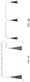
- FIG. 1Ais a schematic diagram of the device layout.
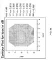
- FIG. 1Bis a diagram showing the contour plot of the simulated electric field intensity distribution at 1550 nm wavelength.
- FIG. 2Ais a graph showing the simulated power transmission as a function of wavelength.
- FIG. 2Bis a graph showing the simulated reflection as a function of wavelength.
- FIG. 3Ais a diagram showing the Y-junction characterization structure for a plurality of cascaded Mach-Zehnder structures to measure insertion loss.
- FIG. 3Bis a diagram showing the Y-junction characterization structure for a single Y-junction to measure coupling ratio and spectrum response.
- FIG. 4Ais a graph showing the typical measured spectra of the test structure in FIG. 3A for different numbers of cascaded Mach-Zehnders.
- FIG. 4Bis a graph showing the typical measured spectra of the test structure in FIG. 3B .
- FIG. 5Ais a graph of power loss as a function of the number of Y-junctions in a cascade.
- the dotsare measured peak optical power from test structure in shown FIG. 3A on Die (0,0).
- the lineis a linear fitting curve.
- FIG. 5Bis a plot of the measured cross-wafer insertion loss of Y-junctions.
- Our devicehas very low loss, small footprint, low wavelength sensitivity and was successfully fabricated by 248 nm CMOS with good cross-wafer uniformity.
- the devicecan be part of a more complicated optoelectronic device, such as a Mach-Zehnder modulator, or a basic building block of integrated silicon photonic circuit.
- the devicecan be a useful component of the process design kit (PDK) of a silicon photonics foundry. Companies commercializing silicon photonics technology, such as modulators and transceivers can also integrate this device in their products.
- PDKprocess design kit
- the deviceachieves low loss, compact, and wavelength insensitive 1 ⁇ 2 power splitting for submicron silicon waveguides. It interfaces with 500 nm ⁇ 200 nm silicon waveguide.
- the power splittercan be readily inserted into other silicon photonic device or circuits as a basic building block. It can be used as a standard GDS cell, similar to p-cells in electronic circuit, such as transistors and resistors.
- the goalwas to design a compact, low loss and wavelength insensitive Y-junction for submicron silicon waveguide, compatible with typical CMOS photonic processes, where 193 nm or 248 nm steppers are commonly used. A minimum feature size of 200 nm was assumed during the design, which will not break the designs rules, thus ensure yield. Silicon waveguide geometry is 500 nm ⁇ 220 nm. So the taper width is 0.5 ⁇ m at input and 1.2 ⁇ m at output, as shown in FIG. 1A . The length of the taper connecting input and output waveguides was set to 2 ⁇ m to keep the device compact.
- Ge-on-Si photodetectorsis usually on the order of 10 ⁇ m, and p-n junction modulator with phase shifter length of 50 ⁇ m has been demonstrated (see, for example, H. C. Nguyen, S. Hashimoto, M. Shinkawa and T. Baba, “Compact and fast photonic crystal silicon optical modulators,” Opt. Express 20, 22465-22474 (2012)).
- a simple passive component like Y-junctionshould be compact enough to be part of a more complicated active device or an integrated optical circuit.
- the Y-junctionis symmetric in the propagation direction to ensure balanced output at two branches.
- FDTDFinite Difference Time Domain
- GGenetic Algorithm
- v n⁇ *v n +c 1 *rand( )/*( p best,n ⁇ x n )+ c 2 *rand( )*( g best,n ⁇ x n ) (2)
- v n and x nare particle's velocity and position in nth dimension of the parameter space
- p best,n and g best,nare individual and global best positions.
- the new velocityis the old velocity scaled by ⁇ and increased the direction of p best,n and g best,n .
- ⁇known as the inertial weight
- c 1determines how much a particle is influenced by the memory of its best position, thus sometimes called cognitive rates.
- c 2is a factor demining how much the particle is affected by the global best position of the whole swarm, hence called social rates.
- the two random numbersare used to simulate the unpredictable behavior of natural swarm. It can be seen that the particle velocity is large when it is far from p best,n and g best,n , becomes smaller as it is closer to the best position and gets pulled back after flying over. The optimization is stopped when the figure of merit is good enough or a large number of iteration is reached.
- FIG. 1Ais a schematic diagram of the device layout.
- FIG. 1Bis a diagram showing the contour plot of the simulated electric field intensity distribution at 1550 nm wavelength.
- the taperwas first digitalized into 13 segments of equal length.
- the width of each segmentlabeled as w 1 to w 13 in FIG. 1A , was optimized to achieve low loss coupling.
- Taper geometryis defined by spline interpolation of these 13 points.
- the optimization figure of merit (FOM)was the power in TEO mode at either branch. It was calculated by the overlap integral of TEO mode of a 500 nm ⁇ 220 nm waveguide with the detected field at the output branch. Note that it is not proper to set the total detected power to be FOM, since higher order modes will leak out of the waveguide along the way. Maximizing the power effectively reduced the scattering and back-reflection. The swarm population was set to 30.
- 2D FDTDwas used as an approximation of 3D FDTD for computation efficiency during optimization.
- a commercially available code wadused (available from http://www.lumerical.com/tcad-products/fdtd/ [16].
- 3D FDTDwas run on this solution to double check the result with a mesh equal to 1/34 of the free space wavelength.
- the insertion losswas determined to be 0.13 dB. No noticeable scattering is seen in the contour plot of electric field intensity as shown in FIG. 1 b . There is an interference pattern at the input end, indicating non-zero back-reflection.
- FIG. 2Ais a graph showing the simulated power transmission as a function of wavelength.
- FIG. 2Bis a graph showing the simulated reflection as a function of wavelength.
- Starting substratewas an 8-inch SOI wafer, with 220 nm, 10 ohm-cm p-type top silicon film, 2 ⁇ m buried oxide on top of a silicon handle.
- Waveguideswere patterned using 248 nm UV lithography followed by dry etching. Then a few microns of oxide were deposited as top cladding.
- Light coupling on and off chipwas achieved by grating couplers (GC).
- GCgrating couplers
- Two kinds of characterization structuresare laid out, as shown in FIG. 3A and FIG. 3B .
- a cascade of Mach-Zehnder structures formed by butt coupled Y-junctionswere used to measure the insertion loss, similar those used in A.
- CMOS photonics platformIEEE J. Sel. Top. Quantum Electron. 17, 597-608 (2011).
- the other structurehas the three terminals of the Y-junction connected to three grating couplers to measure the output directly. In both cases, the bend radius of waveguide is 10 ⁇ m. And grating coupler pitch is 127 ⁇ m, determined by the pitch of fiber array. Simple GC loops, i.e. two GCs connected by a U-turn waveguide, were used as a reference structure. Tiles used around the devices to achieve a certain filling ratio are not shown.
- FIG. 3Ais a diagram showing the Y-junction characterization structure for a plurality of cascaded Mach-Zehnder structures to measure insertion loss.
- FIG. 3Bis a diagram showing the Y-junction characterization structure for a single Y-junction to measure coupling ratio and spectrum response.
- Deviceswere measured on a wafer scale setup that can map the wafer coordinate to the stage coordinate, so that any device can be easily probed after initial alignment.
- Light from a tunable laserwas coupled into the device under test (DUT) via a though a polarization maintaining (PM) fiber and grating coupler, then to a photodetector through another grating coupler and PM fiber.
- Chuck temperaturewas set to 35° C., slightly higher than room temperature. The device performance reported in this paper is not expected as a strong function of temperature. Reticle size on the wafer is 2.5 cm ⁇ 3.2 cm. Test structures shown in FIG. 3A and FIG. 3B in each die were tested to characterize the cross-wafer performance.
- FIG. 4Ais a graph showing the typical measured spectra of the test structure in FIG. 3A for different numbers of cascaded Mach-Zehnders.
- FIG. 4Bis a graph showing the typical measured spectra of the test structure in FIG. 3B .
- Typical spectra structures in FIG. 3A and FIG. 3Bare shown in FIG. 4A and FIG. 4B respectively.
- the parabolic-like shapeis determined by the grating coupler spectrum response.
- the grating coupler design used hereworks only for TE mode and is highly polarization selective. Due to the non-perfect polarization of input light, fringes appear on the spectra. The fringes are usually 0.5 dB peak to peak, and can be reduced by using a polarization controller.
- FIG. 5BA contour plot of insertion loss is shown in FIG. 5B . From the contour, we can see that our device performance is uniform across the wafer, with an average of 0.28 ⁇ 0.02 dB. Low cross-wafer variation confirms that our device is not fabrication sensitive, and can be reliable component of an integrated photonic system.
- the spectra in FIG. 4A and FIG. 4Balso validate the simulation results in FIG. 2A and FIG. 2B , that the device performance is wavelength insensitive.
- FIG. 5Ais a graph of power loss as a function of the number of Y-junctions in a cascade.
- the dotsare measured peak optical power from test structure in shown FIG. 3A on Die (0,0).
- the lineis a linear fitting curve.
- FIG. 5Bis a plot of the measured cross-wafer insertion loss of Y-junctions.
- any reference to an electronic signal or an electromagnetic signalis to be understood as referring to a non-volatile electronic signal or a non-volatile electromagnetic signal.
- Recording the results from an operation or data acquisitionsuch as for example, recording results at a particular frequency or wavelength is understood to mean and is defined herein as writing output data in a non-transitory manner to a storage element, to a machine-readable storage medium, or to a storage device.
- Non-transitory machine-readable storage mediathat can be used in the invention include electronic, magnetic and/or optical storage media, such as magnetic floppy disks and hard disks; a DVD drive, a CD drive that in some embodiments can employ DVD disks, any of CD-ROM disks (i.e., read-only optical storage disks), CD-R disks (i.e., write-once, read-many optical storage disks), and CD-RW disks (i.e., rewriteable optical storage disks); and electronic storage media, such as RAM, ROM, EPROM, Compact Flash cards, PCMCIA cards, or alternatively SD or SDIO memory; and the electronic components (e.g., floppy disk drive, DVD drive, CD/CD-R/CD-RW drive, or Compact Flash/PCMCIA/SD adapter) that accommodate and read from and/or write to the storage media.
- any reference herein to “record” or “recording”is understood to refer to a non-transitory record or
- Recording image data for later usecan be performed to enable the use of the recorded information as output, as data for display to a user, or as data to be made available for later use.
- Such digital memory elements or chipscan be standalone memory devices, or can be incorporated within a device of interest.
- “Writing output data” or “writing an image to memory”is defined herein as including writing transformed data to registers within a microcomputer.
- Microcomputeris defined herein as synonymous with microprocessor, microcontroller, and digital signal processor (“DSP”). It is understood that memory used by the microcomputer, including for example instructions for data processing coded as “firmware” can reside in memory physically inside of a microcomputer chip or in memory external to the microcomputer or in a combination of internal and external memory. Similarly, analog signals can be digitized by a standalone analog to digital converter (“ADC”) or one or more ADCs or multiplexed ADC channels can reside within a microcomputer package. It is also understood that field programmable array (“FPGA”) chips or application specific integrated circuits (“ASIC”) chips can perform microcomputer functions, either in hardware logic, software emulation of a microcomputer, or by a combination of the two. Apparatus having any of the inventive features described herein can operate entirely on one microcomputer or can include more than one microcomputer.
- ADCanalog to digital converter
- FPGAfield programmable array
- ASICapplication specific integrated circuits
- General purpose programmable computers useful for controlling instrumentation, recording signals and analyzing signals or data according to the present descriptioncan be any of a personal computer (PC), a microprocessor based computer, a portable computer, or other type of processing device.
- the general purpose programmable computertypically comprises a central processing unit, a storage or memory unit that can record and read information and programs using machine-readable storage media, a communication terminal such as a wired communication device or a wireless communication device, an output device such as a display terminal, and an input device such as a keyboard.
- the display terminalcan be a touch screen display, in which case it can function as both a display device and an input device.
- Different and/or additional input devicescan be present such as a pointing device, such as a mouse or a joystick, and different or additional output devices can be present such as an enunciator, for example a speaker, a second display, or a printer.
- the computercan run any one of a variety of operating systems, such as for example, any one of several versions of Windows, or of MacOS, or of UNIX, or of Linux. Computational results obtained in the operation of the general purpose computer can be stored for later use, and/or can be displayed to a user.
- each microprocessor-based general purpose computerhas registers that store the results of each computational step within the microprocessor, which results are then commonly stored in cache memory for later use, so that the result can be displayed, recorded to a non-volatile memory, or used in further data processing or analysis.
- any implementation of the transfer functionincluding any combination of hardware, firmware and software implementations of portions or segments of the transfer function, is contemplated herein, so long as at least some of the implementation is performed in hardware.
Landscapes
- Physics & Mathematics (AREA)
- Engineering & Computer Science (AREA)
- General Physics & Mathematics (AREA)
- Optics & Photonics (AREA)
- Theoretical Computer Science (AREA)
- General Engineering & Computer Science (AREA)
- Evolutionary Computation (AREA)
- Biophysics (AREA)
- Life Sciences & Earth Sciences (AREA)
- Health & Medical Sciences (AREA)
- Microelectronics & Electronic Packaging (AREA)
- Computer Hardware Design (AREA)
- Geometry (AREA)
- Bioinformatics & Cheminformatics (AREA)
- Evolutionary Biology (AREA)
- Bioinformatics & Computational Biology (AREA)
- Chemical & Material Sciences (AREA)
- Nanotechnology (AREA)
- Power Engineering (AREA)
- Physiology (AREA)
- Mathematical Physics (AREA)
- Software Systems (AREA)
- Computing Systems (AREA)
- Molecular Biology (AREA)
- General Health & Medical Sciences (AREA)
- Data Mining & Analysis (AREA)
- Computational Linguistics (AREA)
- Biomedical Technology (AREA)
- Artificial Intelligence (AREA)
- Genetics & Genomics (AREA)
- Computer Networks & Wireless Communication (AREA)
- Optical Integrated Circuits (AREA)
Abstract
Description
- This application claims priority to and the benefit of co-pending U.S. provisional patent application Ser. No. 61/731,502, filed Nov. 30, 2012, which application is incorporated herein by reference in its entirety.
- This invention was made with government support under Grant No FA9550-10-1-0053 awarded by the Air Force Office of Scientific Research (AFOSR). The government has certain rights in the invention.
- The invention relates to optical waveguide components in general and particularly to a Y-junction for use with submicron silicon waveguides.
- The last decade witnessed series of break-throughs in silicon photonics. Key components such as the electrically pumped laser (see, for example, R. Camacho-Aguilera, et al, “An electrically pumped germanium laser,” Opt. Express 20, 11316-11320 (2012)), the high-speed modulator (see, for example, G. T. Reed, G. Mashanovish, F. Y. Gardes and D. J. Thomson, “Silicon optical modulators,” Nat. Photonics 4, 518-526 (2010)) and the photodetector (see, for example, J. Michel, J. Liu, and L. C. Kimerling, “High-performance Ge-on-Si photodetectors,” Nat. Photonics, 4, 527-534 (2010)) have been successfully demonstrated. Foundry services are also becoming available to the community, making it easier to explore system level functionalities (see, for example, Y. Zhang, T. Baehr-Jones, R. Ding, T. Pinguet, Z. Xuan, M. Hochberg, “Silicon multi-project wafer platforms for optoelectronic system integration,” Proc. 9th IEEE Intern. Conf. GFP, 2012, and the web sites of opsisfoundry.org and epixfab.eu). The intrinsic advantage of silicon as a photonic material system is its high refractive index contrast over silicon dioxide, allowing submicron waveguides and tight bends, as well as the state-of-the-art CMOS fabrication infrastructure developed by the electronics industry. However, these two advantages do not always go in parallel. For example, a Y-junction is theoretically lossless, while this is generally not the case due to limited resolution of micro fabrication. Sharp corners favored by photonics designs usually violate the minimum feature size rule of a CMOS process, which can be easily caught by design rule checking (DRC) routines. The possible detrimental effects of this violation in fabrication includes peeling off of photoresists, shallower etch in the narrow gap, and voids in subsequent oxide cladding deposition. All the above degrade device performance and lower yield.
- A Y-junction formed by circular bends with a butt waveguide in between to avoid the sharp corner has over 1 dB insertion loss. Mach-Zehnder modulators having two such Y-branches readily have more than 2 dB insertion loss in the budget, regardless of other losses from free carrier absorption and on-and-off chip light coupling, making them less competitive to their III-V counterparts. In addition, complicated integrated optical circuits cannot be built on such lossy components. Moreover, the abrupt waveguide discontinuity causes light scattering and back-reflection. Implicit resonance cavities formed by these scattering sites degrade the system spectrum response.
- As one the most basic building blocks, a low loss and compact Y-junction is very important for silicon photonic circuits. Recently a number of authors have demonstrated attractive device performance for Y-junctions (see, for example, A. Sakai, T. Fukazawa, and T. Baba, “Low loss ultra-small branches in a silicon photonic wire waveguide,” IEICE Trans. Electron. E85-C, 1033-1038 (2002)), MMI couplers (see, for example, D. Van Thourhout, W. Bogaerts, P. Dumon, G. Roelkens, J. Van Campenhout, R. Baets, “Functional silicon wire waveguides,” Proc. Integrated Photonics Research and Applications (2006)), cascaded splitters (see, for example, Z. Wang, Z. Fan, J. Xia, S. Chen and J. Yu, “1×8 cascaded multimode interference splitter in silicon-on-insulator,” Jpn. J. Appl. Phys. 43, 5085-5087 (2004) and S. H. Tao, Q. Fang, J. F. Song, M. B. Yu, G. Q. Lo, and D. L. Kwong, “Cascaded wide-angle Y-
junction 1×16 power splitter based on silicon wire waveguides on silicon-on-insulator,” Opt. Express 16, 21456-21461 (2008)),photonic crystal 3 dB couplers (see, for example, L. H. Frandsen, et al, “Ultralow-loss 3 dB photonic crystal waveguide splitter,” Opt. Lett. 29, 1623-1625 (2004)) and directional couplers (see, for example, H. Yamada, T. Chu, S. Ishida, and Y. Arakawa, “Optical directional coupler based on Si-wire waveguides,” IEEE Photonics Technol. Lett. 17, 585-587 (2005)). However, a Y-junction with low excess loss, low wavelength sensitivity, small footprint, and dimensions clearly within the typical design rules of a modern CMOS photonics process has remained elusive. - The 1×3 power splitter function can be achieved by multi-mode interference (MMI) couplers or directional couplers. Usually these devices have large insertion loss, large footprint, high wavelength sensitivity or low compatibility with CMOS fabrication methods.
- There is a need for an efficient Y-junction device that can be manufactured easily.
- According to one aspect, the invention features a 1×2 power splitter for use in submicron silicon waveguides. The 1×2 power splitter comprises an input port configured to receive an optical signal having a power of substantially P watts; and a pair of output ports configured to provide substantially equal output signals each having a power of substantially P/2 Watts; the 1×2 power splitter having a footprint of less than 1.2 μm×2 μm in area.
- In one embodiment, the input port has a taper width of 0.5 μm.
- In another embodiment, at least one of the output ports has taper width of 0.5 μm.
- In yet another embodiment, the 1×2 power splitter has a total output width of 1.2 μm.
- In still another embodiment, the 1×2 power splitter has a minimum feature size of 200 nm.
- In a further embodiment, the 1×2 power splitter is configured to be manufactured using a CMOS fabrication process.
- In yet a further embodiment, the CMOS fabrication process is a process conducted using a 248 nm stepper.
- In an additional embodiment, the CMOS fabrication process is a process conducted using a 193 nm stepper.
- The foregoing and other objects, aspects, features, and advantages of the invention will become more apparent from the following description and from the claims.
- The objects and features of the invention can be better understood with reference to the drawings described below, and the claims. The drawings are not necessarily to scale, emphasis instead generally being placed upon illustrating the principles of the invention. In the drawings, like numerals are used to indicate like parts throughout the various views.
FIG. 1A is a schematic diagram of the device layout.FIG. 1B is a diagram showing the contour plot of the simulated electric field intensity distribution at 1550 nm wavelength.FIG. 2A is a graph showing the simulated power transmission as a function of wavelength.FIG. 2B is a graph showing the simulated reflection as a function of wavelength.FIG. 3A is a diagram showing the Y-junction characterization structure for a plurality of cascaded Mach-Zehnder structures to measure insertion loss.FIG. 3B is a diagram showing the Y-junction characterization structure for a single Y-junction to measure coupling ratio and spectrum response.FIG. 4A is a graph showing the typical measured spectra of the test structure inFIG. 3A for different numbers of cascaded Mach-Zehnders.FIG. 4B is a graph showing the typical measured spectra of the test structure inFIG. 3B .FIG. 5A is a graph of power loss as a function of the number of Y-junctions in a cascade. The dots are measured peak optical power from test structure in shownFIG. 3A on Die (0,0). The line is a linear fitting curve.FIG. 5B is a plot of the measured cross-wafer insertion loss of Y-junctions.- We have designed a compact, low-loss and wavelength insensitive Y-junction for submicron silicon waveguide using FDTD and particle swarm optimization (PSO), and fabricated the device in a 248 nm CMOS line. We have measured an average insertion loss of 0.28±0.02 dB across an 8-inch wafer. The device footprint is less than 1.2 μm×2 μm, orders of magnitude smaller than MMI and directional couplers. The function of the invention is to provide a 1×2 power splitter for submicron silicon waveguides.
- Our device has very low loss, small footprint, low wavelength sensitivity and was successfully fabricated by 248 nm CMOS with good cross-wafer uniformity.
- The device can be part of a more complicated optoelectronic device, such as a Mach-Zehnder modulator, or a basic building block of integrated silicon photonic circuit.
- The device can be a useful component of the process design kit (PDK) of a silicon photonics foundry. Companies commercializing silicon photonics technology, such as modulators and transceivers can also integrate this device in their products.
- The device achieves low loss, compact, and wavelength insensitive 1×2 power splitting for submicron silicon waveguides. It interfaces with 500 nm×200 nm silicon waveguide. The power splitter can be readily inserted into other silicon photonic device or circuits as a basic building block. It can be used as a standard GDS cell, similar to p-cells in electronic circuit, such as transistors and resistors.
- We modeled the electro-magnetic response of the structure using finite difference time domain (FDTD) method, and optimized the device geometry using particle swarm simulation (PSO).
- We have designed and fabricated a Y-junction for submicron silicon waveguide with a taper less than 1.2 μm×2 μm, and cross-wafer average insertion loss 0.28±0.02 dB, comparable to the result demonstrated by electron beam lithography (EBL) and MMIs with much larger footprint. The coupling ratio is wavelength insensitive. The device has a minimum feature size of 200 nm, and successfully fabricated using 248 nm lithography.
- The goal was to design a compact, low loss and wavelength insensitive Y-junction for submicron silicon waveguide, compatible with typical CMOS photonic processes, where 193 nm or 248 nm steppers are commonly used. A minimum feature size of 200 nm was assumed during the design, which will not break the designs rules, thus ensure yield. Silicon waveguide geometry is 500 nm×220 nm. So the taper width is 0.5 μm at input and 1.2 μm at output, as shown in
FIG. 1A . The length of the taper connecting input and output waveguides was set to 2 μm to keep the device compact. The size of Ge-on-Si photodetectors is usually on the order of 10 μm, and p-n junction modulator with phase shifter length of 50 μm has been demonstrated (see, for example, H. C. Nguyen, S. Hashimoto, M. Shinkawa and T. Baba, “Compact and fast photonic crystal silicon optical modulators,” Opt. Express 20, 22465-22474 (2012)). A simple passive component like Y-junction should be compact enough to be part of a more complicated active device or an integrated optical circuit. The Y-junction is symmetric in the propagation direction to ensure balanced output at two branches. - The electromagnetic response of dielectric structures of size on the order of wavelength of interest can be simulated by Finite Difference Time Domain (FDTD) method. FDTD can be coupled with optimization algorithms to for design optimization. Sanchis et al demonstrated a waveguide crossing with 0.2 dB insertion loss and −40 dB cross-talk designed by FDTD and Genetic Algorithm (GA) (see, for example, P. Sanchis, et al, “Highly efficient crossing structure for silicon-on-insulator waveguides,” Opt. Lett. 34, 2760-2762 (2009)). We utilized a different optimization algorithm, Particle Swarm Optimization (PSO), in this design. PSO is initially inspired by the social behavior of flocks of birds or schools of fish (see, for example, J. Kennedy and R. Eberhart, “Particle swarm optimization,” Proc. IEEE Intern. Conf. Neural Networks (1995)), and has been successfully applied to electromagnetic optimization problems (see, for example, J. Robinson and Y. Rhamat-Samii, “Particle swarm optimization in electromagnetics,” IEEE Trans. Antennas Propag. 52, 397-407 (2004)). In PSO, the potential solutions, called particles or agents, are initialized at random positions with random velocities in the parameter space. A figure of merit function is defined to evaluate the particle position according to the optimization goal. The best position for each individual particle is recorded, as well as a global best position ever achieved by any particle in the swarm. The position of a particle is updated by the following equation,
xn×xn+Δt*vn (1)
vn=ω*vn+c1*rand( )/*(pbest,n−xn)+c2*rand( )*(gbest,n−xn) (2)- where vnand xnare particle's velocity and position in nth dimension of the parameter space, and pbest,nand gbest,nare individual and global best positions. As is apparent from Eq. 2, the new velocity is the old velocity scaled by ω and increased the direction of pbest,nand gbest,n.
- ω, known as the inertial weight, is a measurement of how much a particle would like to stay at the old velocity. c1determines how much a particle is influenced by the memory of its best position, thus sometimes called cognitive rates. And c2is a factor demining how much the particle is affected by the global best position of the whole swarm, hence called social rates. The two random numbers are used to simulate the unpredictable behavior of natural swarm. It can be seen that the particle velocity is large when it is far from pbest,nand gbest,n, becomes smaller as it is closer to the best position and gets pulled back after flying over. The optimization is stopped when the figure of merit is good enough or a large number of iteration is reached.
FIG. 1A is a schematic diagram of the device layout.FIG. 1B is a diagram showing the contour plot of the simulated electric field intensity distribution at 1550 nm wavelength.- In this design, the taper was first digitalized into 13 segments of equal length. The width of each segment, labeled as w1 to w13 in
FIG. 1A , was optimized to achieve low loss coupling. Taper geometry is defined by spline interpolation of these 13 points. The optimization figure of merit (FOM) was the power in TEO mode at either branch. It was calculated by the overlap integral of TEO mode of a 500 nm×220 nm waveguide with the detected field at the output branch. Note that it is not proper to set the total detected power to be FOM, since higher order modes will leak out of the waveguide along the way. Maximizing the power effectively reduced the scattering and back-reflection. The swarm population was set to 30. 2D FDTD was used as an approximation of 3D FDTD for computation efficiency during optimization. A commercially available code wad used (available from http://www.lumerical.com/tcad-products/fdtd/ [16]. Within 50 iterations, one solution with sub-0.2 dB insertion loss emerged, as shown in Table 1. Then 3D FDTD was run on this solution to double check the result with a mesh equal to 1/34 of the free space wavelength. The insertion loss was determined to be 0.13 dB. No noticeable scattering is seen in the contour plot of electric field intensity as shown inFIG. 1b . There is an interference pattern at the input end, indicating non-zero back-reflection. Due to the root square relationship between field magnitude and optical intensity, very weak back-reflection is necessary to create clear interference patterns. The normalized transmission and reflection power as a function of wavelength is plotted inFIG. 2A andFIG. 2B . It can be seen that both the transmission and reflection are wavelength insensitive, with variation below 1% and 0.5% over wavelength range from 1500 nm to 1580 nm. TABLE 1 Taper width in μm w1 w2 w3 w4 w5 w6 w7 w8 w9 w10 w11 w12 w13 0.5 0.5 0.6 0.7 0.9 1.26 1.4 1.4 1.4 1.4 1.31 1.2 1.2 FIG. 2A is a graph showing the simulated power transmission as a function of wavelength.FIG. 2B is a graph showing the simulated reflection as a function of wavelength.- Starting substrate was an 8-inch SOI wafer, with 220 nm, 10 ohm-cm p-type top silicon film, 2 μm buried oxide on top of a silicon handle. Waveguides were patterned using 248 nm UV lithography followed by dry etching. Then a few microns of oxide were deposited as top cladding. Light coupling on and off chip was achieved by grating couplers (GC). Two kinds of characterization structures are laid out, as shown in
FIG. 3A andFIG. 3B . A cascade of Mach-Zehnder structures formed by butt coupled Y-junctions were used to measure the insertion loss, similar those used in A. Mekis, et al, “A grating-coupler-enabled CMOS photonics platform,” IEEE J. Sel. Top. Quantum Electron. 17, 597-608 (2011). The other structure has the three terminals of the Y-junction connected to three grating couplers to measure the output directly. In both cases, the bend radius of waveguide is 10 μm. And grating coupler pitch is 127 μm, determined by the pitch of fiber array. Simple GC loops, i.e. two GCs connected by a U-turn waveguide, were used as a reference structure. Tiles used around the devices to achieve a certain filling ratio are not shown. FIG. 3A is a diagram showing the Y-junction characterization structure for a plurality of cascaded Mach-Zehnder structures to measure insertion loss.FIG. 3B is a diagram showing the Y-junction characterization structure for a single Y-junction to measure coupling ratio and spectrum response.- Devices were measured on a wafer scale setup that can map the wafer coordinate to the stage coordinate, so that any device can be easily probed after initial alignment. Light from a tunable laser was coupled into the device under test (DUT) via a though a polarization maintaining (PM) fiber and grating coupler, then to a photodetector through another grating coupler and PM fiber. Chuck temperature was set to 35° C., slightly higher than room temperature. The device performance reported in this paper is not expected as a strong function of temperature. Reticle size on the wafer is 2.5 cm×3.2 cm. Test structures shown in
FIG. 3A andFIG. 3B in each die were tested to characterize the cross-wafer performance. FIG. 4A is a graph showing the typical measured spectra of the test structure inFIG. 3A for different numbers of cascaded Mach-Zehnders.FIG. 4B is a graph showing the typical measured spectra of the test structure inFIG. 3B .- Typical spectra structures in
FIG. 3A andFIG. 3B are shown inFIG. 4A andFIG. 4B respectively. The parabolic-like shape is determined by the grating coupler spectrum response. The grating coupler design used here works only for TE mode and is highly polarization selective. Due to the non-perfect polarization of input light, fringes appear on the spectra. The fringes are usually 0.5 dB peak to peak, and can be reduced by using a polarization controller. - It is difficult to measure sub-0.5 dB insertion loss from a single device. Therefore, test structures with different numbers of Y-junctions in the loop were used to figure out the insertion loss. The measured peak power as a function of number of Y-junctions in the loop is plotted in
FIG. 5A . Dots are test data, and the line is linear fitting. The slope of the line gives insertion loss in dB per Y-junction. Loop baseline losses, such as grating coupler insertion loss, are the same for all structures, thus won't affect the slope of the fitting line. We measured the insertion loss of all Y-junctions across the wafer. - A contour plot of insertion loss is shown in
FIG. 5B . From the contour, we can see that our device performance is uniform across the wafer, with an average of 0.28±0.02 dB. Low cross-wafer variation confirms that our device is not fabrication sensitive, and can be reliable component of an integrated photonic system. - We also note that the spectra of characterization structures in
FIG. 4A do not deviate from a reference GC spectrum, with only a linear offset in y-axis, even with a large number of Y-junctions in the loop. This validates our estimation that although there is an interference pattern inFIG. 1B the back-reflection is negligible and won't degrade the system spectrum response. - It is shown in S. H. Tao, Q. Fang, J. F. Song, M. B. Yu, G. Q. Lo, and D. L. Kwong, “Cascaded wide-angle Y-
junction 1×16 power splitter based on silicon wire waveguides on silicon-on-insulator,” Opt. Express 16, 21456-21461 (2008) that etch residues or air voids in the gap defined by sharp corners in the layout will lead to non-uniform output at two branches of the Y-junction. InFIG. 4B , the spectra of two branches overlaps over the whole testing wavelength range, indicating balanced output power. So our design fully addressed the DRC violation issue of conventional Y-junctions. - The spectra in
FIG. 4A andFIG. 4B also validate the simulation results inFIG. 2A andFIG. 2B , that the device performance is wavelength insensitive. FIG. 5A is a graph of power loss as a function of the number of Y-junctions in a cascade. The dots are measured peak optical power from test structure in shownFIG. 3A on Die (0,0). The line is a linear fitting curve.FIG. 5B is a plot of the measured cross-wafer insertion loss of Y-junctions.- Our result also confirms PSO as an efficient optimization algorithm for silicon photonic device design and optimization. We utilized moderate swarm population and iteration cycle. It is possible that even better device geometry will emerge with more dedicated optimization. This design method can be readily used address other challenges such as non-uniform grating couplers and distributed brag gratings (DBRs).
- Optical Waveguides and their Uses
- We have described various optical waveguide systems and application, as well as fabrication techniques for such waveguides in a number of patent documents, including U.S. Pat. Nos. 7,200,308, 7,424,192, 7,480,434, 7,643,714, and 7,760,970.
- Unless otherwise explicitly recited herein, any reference to an electronic signal or an electromagnetic signal (or their equivalents) is to be understood as referring to a non-volatile electronic signal or a non-volatile electromagnetic signal.
- Recording the results from an operation or data acquisition, such as for example, recording results at a particular frequency or wavelength is understood to mean and is defined herein as writing output data in a non-transitory manner to a storage element, to a machine-readable storage medium, or to a storage device. Non-transitory machine-readable storage media that can be used in the invention include electronic, magnetic and/or optical storage media, such as magnetic floppy disks and hard disks; a DVD drive, a CD drive that in some embodiments can employ DVD disks, any of CD-ROM disks (i.e., read-only optical storage disks), CD-R disks (i.e., write-once, read-many optical storage disks), and CD-RW disks (i.e., rewriteable optical storage disks); and electronic storage media, such as RAM, ROM, EPROM, Compact Flash cards, PCMCIA cards, or alternatively SD or SDIO memory; and the electronic components (e.g., floppy disk drive, DVD drive, CD/CD-R/CD-RW drive, or Compact Flash/PCMCIA/SD adapter) that accommodate and read from and/or write to the storage media. Unless otherwise explicitly recited, any reference herein to “record” or “recording” is understood to refer to a non-transitory record or a non-transitory recording.
- As is known to those of skill in the machine-readable storage media arts, new media and formats for data storage are continually being devised, and any convenient, commercially available storage medium and corresponding read/write device that may become available in the future is likely to be appropriate for use, especially if it provides any of a greater storage capacity, a higher access speed, a smaller size, and a lower cost per bit of stored information. Well known older machine-readable media are also available for use under certain conditions, such as punched paper tape or cards, magnetic recording on tape or wire, optical or magnetic reading of printed characters (e.g., OCR and magnetically encoded symbols) and machine-readable symbols such as one and two dimensional bar codes. Recording image data for later use (e.g., writing an image to memory or to digital memory) can be performed to enable the use of the recorded information as output, as data for display to a user, or as data to be made available for later use. Such digital memory elements or chips can be standalone memory devices, or can be incorporated within a device of interest. “Writing output data” or “writing an image to memory” is defined herein as including writing transformed data to registers within a microcomputer.
- “Microcomputer” is defined herein as synonymous with microprocessor, microcontroller, and digital signal processor (“DSP”). It is understood that memory used by the microcomputer, including for example instructions for data processing coded as “firmware” can reside in memory physically inside of a microcomputer chip or in memory external to the microcomputer or in a combination of internal and external memory. Similarly, analog signals can be digitized by a standalone analog to digital converter (“ADC”) or one or more ADCs or multiplexed ADC channels can reside within a microcomputer package. It is also understood that field programmable array (“FPGA”) chips or application specific integrated circuits (“ASIC”) chips can perform microcomputer functions, either in hardware logic, software emulation of a microcomputer, or by a combination of the two. Apparatus having any of the inventive features described herein can operate entirely on one microcomputer or can include more than one microcomputer.
- General purpose programmable computers useful for controlling instrumentation, recording signals and analyzing signals or data according to the present description can be any of a personal computer (PC), a microprocessor based computer, a portable computer, or other type of processing device. The general purpose programmable computer typically comprises a central processing unit, a storage or memory unit that can record and read information and programs using machine-readable storage media, a communication terminal such as a wired communication device or a wireless communication device, an output device such as a display terminal, and an input device such as a keyboard. The display terminal can be a touch screen display, in which case it can function as both a display device and an input device. Different and/or additional input devices can be present such as a pointing device, such as a mouse or a joystick, and different or additional output devices can be present such as an enunciator, for example a speaker, a second display, or a printer. The computer can run any one of a variety of operating systems, such as for example, any one of several versions of Windows, or of MacOS, or of UNIX, or of Linux. Computational results obtained in the operation of the general purpose computer can be stored for later use, and/or can be displayed to a user. At the very least, each microprocessor-based general purpose computer has registers that store the results of each computational step within the microprocessor, which results are then commonly stored in cache memory for later use, so that the result can be displayed, recorded to a non-volatile memory, or used in further data processing or analysis.
- Many functions of electrical and electronic apparatus can be implemented in hardware (for example, hard-wired logic), in software (for example, logic encoded in a program operating on a general purpose processor), and in firmware (for example, logic encoded in a non-volatile memory that is invoked for operation on a processor as required). The present invention contemplates the substitution of one implementation of hardware, firmware and software for another implementation of the equivalent functionality using a different one of hardware, firmware and software. To the extent that an implementation can be represented mathematically by a transfer function, that is, a specified response is generated at an output terminal for a specific excitation applied to an input terminal of a “black box” exhibiting the transfer function, any implementation of the transfer function, including any combination of hardware, firmware and software implementations of portions or segments of the transfer function, is contemplated herein, so long as at least some of the implementation is performed in hardware.
- Although the theoretical description given herein is thought to be correct, the operation of the devices described and claimed herein does not depend upon the accuracy or validity of the theoretical description. That is, later theoretical developments that may explain the observed results on a basis different from the theory presented herein will not detract from the inventions described herein.
- Any patent, patent application, patent application publication, journal article, book, published paper, or other publicly available material identified in the specification is hereby incorporated by reference herein in its entirety. Any material, or portion thereof, that is said to be incorporated by reference herein, but which conflicts with existing definitions, statements, or other disclosure material explicitly set forth herein is only incorporated to the extent that no conflict arises between that incorporated material and the present disclosure material. In the event of a conflict, the conflict is to be resolved in favor of the present disclosure as the preferred disclosure.
- While the present invention has been particularly shown and described with reference to the preferred mode as illustrated in the drawing, it will be understood by one skilled in the art that various changes in detail may be affected therein without departing from the spirit and scope of the invention as defined by the claims.
Claims (21)
Priority Applications (1)
| Application Number | Priority Date | Filing Date | Title |
|---|---|---|---|
| US16/214,365US11036004B2 (en) | 2012-11-30 | 2018-12-10 | Compact and low loss Y-junction for submicron silicon waveguide |
Applications Claiming Priority (6)
| Application Number | Priority Date | Filing Date | Title |
|---|---|---|---|
| US201261731502P | 2012-11-30 | 2012-11-30 | |
| US14/093,263US9217829B2 (en) | 2012-11-30 | 2013-11-29 | Compact and low loss Y-junction for submicron silicon waveguide |
| US14/834,597US20160033765A1 (en) | 2012-11-30 | 2015-08-25 | Compact and low loss y-junction for submicron silicon waveguide |
| US15/446,375US9851503B2 (en) | 2012-11-30 | 2017-03-01 | Compact and low loss Y-junction for submicron silicon waveguide |
| US15/825,266US10185087B2 (en) | 2012-11-30 | 2017-11-29 | Compact and low loss Y-junction for submicron silicon waveguide |
| US16/214,365US11036004B2 (en) | 2012-11-30 | 2018-12-10 | Compact and low loss Y-junction for submicron silicon waveguide |
Related Parent Applications (1)
| Application Number | Title | Priority Date | Filing Date |
|---|---|---|---|
| US15/825,266ContinuationUS10185087B2 (en) | 2012-11-30 | 2017-11-29 | Compact and low loss Y-junction for submicron silicon waveguide |
Publications (2)
| Publication Number | Publication Date |
|---|---|
| US20200026002A1true US20200026002A1 (en) | 2020-01-23 |
| US11036004B2 US11036004B2 (en) | 2021-06-15 |
Family
ID=50974769
Family Applications (6)
| Application Number | Title | Priority Date | Filing Date |
|---|---|---|---|
| US14/093,263Active2034-03-01US9217829B2 (en) | 2012-11-30 | 2013-11-29 | Compact and low loss Y-junction for submicron silicon waveguide |
| US14/834,597AbandonedUS20160033765A1 (en) | 2012-11-30 | 2015-08-25 | Compact and low loss y-junction for submicron silicon waveguide |
| US14/940,097AbandonedUS20170131470A1 (en) | 2012-11-30 | 2015-11-12 | Compact and low loss Y-junction for submicron silicon waveguide |
| US15/446,375ActiveUS9851503B2 (en) | 2012-11-30 | 2017-03-01 | Compact and low loss Y-junction for submicron silicon waveguide |
| US15/825,266ActiveUS10185087B2 (en) | 2012-11-30 | 2017-11-29 | Compact and low loss Y-junction for submicron silicon waveguide |
| US16/214,365ActiveUS11036004B2 (en) | 2012-11-30 | 2018-12-10 | Compact and low loss Y-junction for submicron silicon waveguide |
Family Applications Before (5)
| Application Number | Title | Priority Date | Filing Date |
|---|---|---|---|
| US14/093,263Active2034-03-01US9217829B2 (en) | 2012-11-30 | 2013-11-29 | Compact and low loss Y-junction for submicron silicon waveguide |
| US14/834,597AbandonedUS20160033765A1 (en) | 2012-11-30 | 2015-08-25 | Compact and low loss y-junction for submicron silicon waveguide |
| US14/940,097AbandonedUS20170131470A1 (en) | 2012-11-30 | 2015-11-12 | Compact and low loss Y-junction for submicron silicon waveguide |
| US15/446,375ActiveUS9851503B2 (en) | 2012-11-30 | 2017-03-01 | Compact and low loss Y-junction for submicron silicon waveguide |
| US15/825,266ActiveUS10185087B2 (en) | 2012-11-30 | 2017-11-29 | Compact and low loss Y-junction for submicron silicon waveguide |
Country Status (1)
| Country | Link |
|---|---|
| US (6) | US9217829B2 (en) |
Cited By (1)
| Publication number | Priority date | Publication date | Assignee | Title |
|---|---|---|---|---|
| WO2024189249A1 (en) | 2023-03-10 | 2024-09-19 | Consejo Superior De Investigaciones Científicas (Csic) | Power-splitting device integrated into waveguides |
Families Citing this family (33)
| Publication number | Priority date | Publication date | Assignee | Title |
|---|---|---|---|---|
| US20130058611A1 (en)* | 2011-09-01 | 2013-03-07 | Feng Shi | Photonic crystal optical waveguide solar spectrum splitter |
| US9217829B2 (en) | 2012-11-30 | 2015-12-22 | Coriant Advanced Technology, LLC | Compact and low loss Y-junction for submicron silicon waveguide |
| WO2016134323A1 (en) | 2015-02-19 | 2016-08-25 | Coriant Advanced Technology, LLC | Integrated polarization splitter and rotator |
| US9588298B2 (en)* | 2015-06-04 | 2017-03-07 | Elenion Technologies, Llc | Edge coupler |
| BR112017023036A2 (en) | 2015-06-04 | 2018-07-03 | Halliburton Energy Services Inc | integrated computational method and element |
| US9874693B2 (en) | 2015-06-10 | 2018-01-23 | The Research Foundation For The State University Of New York | Method and structure for integrating photonics with CMOs |
| US9557486B2 (en)* | 2015-06-29 | 2017-01-31 | Elenion Technologies, Llc | Optimized 2×2 3dB multi-mode interference coupler |
| US9739947B2 (en)* | 2015-06-29 | 2017-08-22 | Elenion Technologies, Llc | Multi-mode interference coupler |
| WO2017049276A2 (en)* | 2015-09-18 | 2017-03-23 | Elenion Technologies, Llc | Methods for designing photonic devices |
| US9946020B1 (en)* | 2017-02-03 | 2018-04-17 | Elenion Technologies, Llc | Mode matched Y-junction |
| US10514499B2 (en) | 2018-01-19 | 2019-12-24 | Elenion Technologies, Llc | Photonic chip with an input wavelength filter |
| US11205022B2 (en) | 2019-01-10 | 2021-12-21 | X Development Llc | System and method for optimizing physical characteristics of a physical device |
| US10615869B1 (en) | 2019-01-10 | 2020-04-07 | X Development Llc | Physical electromagnetics simulator for design optimization of photonic devices |
| US11550971B1 (en) | 2019-01-18 | 2023-01-10 | X Development Llc | Physics simulation on machine-learning accelerated hardware platforms |
| US11295212B1 (en) | 2019-04-23 | 2022-04-05 | X Development Llc | Deep neural networks via physical electromagnetics simulator |
| US11238190B1 (en) | 2019-04-23 | 2022-02-01 | X Development Llc | Physical device optimization with reduced computational latency via low-rank objectives |
| US11900026B1 (en) | 2019-04-24 | 2024-02-13 | X Development Llc | Learned fabrication constraints for optimizing physical devices |
| US11397895B2 (en) | 2019-04-24 | 2022-07-26 | X Development Llc | Neural network inference within physical domain via inverse design tool |
| US11106841B1 (en) | 2019-04-29 | 2021-08-31 | X Development Llc | Physical device optimization with reduced memory footprint via time reversal at absorbing boundaries |
| US11501169B1 (en) | 2019-04-30 | 2022-11-15 | X Development Llc | Compressed field response representation for memory efficient physical device simulation |
| US11003814B1 (en) | 2019-05-22 | 2021-05-11 | X Development Llc | Optimization of physical devices via adaptive filter techniques |
| CN110187499B (en)* | 2019-05-29 | 2021-10-19 | 哈尔滨工业大学(深圳) | A Design Method of On-Chip Optical Power Attenuator Based on Neural Network |
| US11379633B2 (en) | 2019-06-05 | 2022-07-05 | X Development Llc | Cascading models for optimization of fabrication and design of a physical device |
| US10862610B1 (en) | 2019-11-11 | 2020-12-08 | X Development Llc | Multi-channel integrated photonic wavelength demultiplexer |
| US11187854B2 (en) | 2019-11-15 | 2021-11-30 | X Development Llc | Two-channel integrated photonic wavelength demultiplexer |
| CN111274673B (en)* | 2020-01-07 | 2021-02-23 | 上海索辰信息科技股份有限公司 | Optical product model optimization method and system based on particle swarm optimization |
| US11280961B1 (en)* | 2020-12-07 | 2022-03-22 | Globalfoundries U.S. Inc. | Optical power splitters with side-confining elements |
| CN112987289B (en)* | 2021-02-05 | 2022-09-20 | 中国科学院微电子研究所 | A parameter optimization method for waveguide structure |
| US12153662B2 (en) | 2021-04-05 | 2024-11-26 | X Development Llc | Metastructured photonic device authentication |
| US11536907B2 (en) | 2021-04-21 | 2022-12-27 | X Development Llc | Cascaded integrated photonic wavelength demultiplexer |
| US20230030875A1 (en)* | 2021-07-28 | 2023-02-02 | Hewlett Packard Enterprise Development Lp | Photodetector behavior modeling |
| US11962351B2 (en) | 2021-12-01 | 2024-04-16 | X Development Llc | Multilayer photonic devices with metastructured layers |
| US11609392B1 (en)* | 2022-02-24 | 2023-03-21 | X Development Llc | Photonic coupler |
Citations (2)
| Publication number | Priority date | Publication date | Assignee | Title |
|---|---|---|---|---|
| US20120311516A1 (en)* | 2004-08-02 | 2012-12-06 | Nippon Telegraph And Telephone Corporation | Planar Lightwave Circuit, Design Method for Wave Propagation Circuit, and Computer Program |
| US9915781B1 (en)* | 2017-03-28 | 2018-03-13 | Inphi Corporation | Silicon-waveguide-based broadband polarization splitter-rotator |
Family Cites Families (25)
| Publication number | Priority date | Publication date | Assignee | Title |
|---|---|---|---|---|
| JP3066868B2 (en)* | 1989-11-15 | 2000-07-17 | 三菱瓦斯化学株式会社 | Optical splitter |
| JP3102874B2 (en)* | 1990-11-05 | 2000-10-23 | 日本板硝子株式会社 | Y-branch optical circuit |
| DE69417986T2 (en)* | 1993-11-01 | 1999-09-30 | Sumitomo Electric Industries, Ltd. | Optical branch element |
| US6792172B1 (en)* | 1998-05-08 | 2004-09-14 | The Trustees Of Columbia University Of The City Of New York | Reduced size multimode interference based coupler |
| US6236784B1 (en)* | 1998-08-10 | 2001-05-22 | Hitachi, Ltd. | Y branching optical waveguide and optical integrated circuit |
| KR100417001B1 (en)* | 2001-12-17 | 2004-02-05 | 삼성전자주식회사 | Optical power splitter with assistant waveguide |
| CA2488263A1 (en)* | 2002-06-04 | 2003-12-11 | Nkt Integration A/S | Integrated splitter with reduced losses |
| US7317853B2 (en)* | 2003-08-19 | 2008-01-08 | Ignis Technologies As | Integrated optics spot size converter and manufacturing method |
| US20060039646A1 (en)* | 2004-08-20 | 2006-02-23 | Keiichi Nashimoto | Optical switch and matrix optical switch |
| JP4732806B2 (en)* | 2005-06-06 | 2011-07-27 | 日本電信電話株式会社 | Quartz-based Y-branch optical circuit and manufacturing method thereof |
| US7200308B2 (en) | 2005-06-28 | 2007-04-03 | California Institute Of Technology | Frequency conversion with nonlinear optical polymers and high index contrast waveguides |
| US7643714B2 (en)* | 2005-06-28 | 2010-01-05 | California Institute Of Technology | Nanophotonic devices in silicon |
| US7424192B2 (en) | 2005-06-28 | 2008-09-09 | California Institute Of Technology | Frequency conversion with nonlinear optical polymers and high index contrast waveguides |
| US7480434B2 (en) | 2006-07-25 | 2009-01-20 | California Institute Of Technology | Low loss terahertz waveguides, and terahertz generation with nonlinear optical systems |
| CN101641622B (en)* | 2007-03-20 | 2011-09-14 | 日本电气株式会社 | Optical waveguide and spot size converter using this |
| US7760970B2 (en) | 2007-10-11 | 2010-07-20 | California Institute Of Technology | Single photon absorption all-optical modulator in silicon |
| US8031991B2 (en)* | 2008-05-28 | 2011-10-04 | Lightwire Inc. | Low index, large mode field diameter optical coupler |
| JP2012014027A (en)* | 2010-07-02 | 2012-01-19 | Oki Electric Ind Co Ltd | Star coupler and optical multiplexing/demultiplexing device |
| US20130330036A1 (en)* | 2012-06-06 | 2013-12-12 | International Business Machines Corporation | Exciting a selected mode in an optical waveguide |
| US8627240B1 (en) | 2012-06-28 | 2014-01-07 | International Business Machines Corporation | Integrated design environment for nanophotonics |
| US9217829B2 (en) | 2012-11-30 | 2015-12-22 | Coriant Advanced Technology, LLC | Compact and low loss Y-junction for submicron silicon waveguide |
| US9435946B2 (en)* | 2013-07-23 | 2016-09-06 | National Institute Of Advanced Industrial Science And Technology | Interlayer light wave coupling device |
| TWI512418B (en)* | 2013-07-26 | 2015-12-11 | Nat Univ Tsing Hua | A five axis flank milling system for machining curved surface and a toolpath planning method thereof |
| EP2924482B1 (en)* | 2014-03-26 | 2017-12-20 | Huawei Technologies Co., Ltd. | Polarisation mode converter with an asymmetric silicon nitride waveguide |
| US9557486B2 (en)* | 2015-06-29 | 2017-01-31 | Elenion Technologies, Llc | Optimized 2×2 3dB multi-mode interference coupler |
- 2013
- 2013-11-29USUS14/093,263patent/US9217829B2/enactiveActive
- 2015
- 2015-08-25USUS14/834,597patent/US20160033765A1/ennot_activeAbandoned
- 2015-11-12USUS14/940,097patent/US20170131470A1/ennot_activeAbandoned
- 2017
- 2017-03-01USUS15/446,375patent/US9851503B2/enactiveActive
- 2017-11-29USUS15/825,266patent/US10185087B2/enactiveActive
- 2018
- 2018-12-10USUS16/214,365patent/US11036004B2/enactiveActive
Patent Citations (2)
| Publication number | Priority date | Publication date | Assignee | Title |
|---|---|---|---|---|
| US20120311516A1 (en)* | 2004-08-02 | 2012-12-06 | Nippon Telegraph And Telephone Corporation | Planar Lightwave Circuit, Design Method for Wave Propagation Circuit, and Computer Program |
| US9915781B1 (en)* | 2017-03-28 | 2018-03-13 | Inphi Corporation | Silicon-waveguide-based broadband polarization splitter-rotator |
Cited By (1)
| Publication number | Priority date | Publication date | Assignee | Title |
|---|---|---|---|---|
| WO2024189249A1 (en) | 2023-03-10 | 2024-09-19 | Consejo Superior De Investigaciones Científicas (Csic) | Power-splitting device integrated into waveguides |
Also Published As
| Publication number | Publication date |
|---|---|
| US9851503B2 (en) | 2017-12-26 |
| US20160033765A1 (en) | 2016-02-04 |
| US20170235046A1 (en) | 2017-08-17 |
| US20180081116A1 (en) | 2018-03-22 |
| US11036004B2 (en) | 2021-06-15 |
| US20170131470A1 (en) | 2017-05-11 |
| US10185087B2 (en) | 2019-01-22 |
| US20140178005A1 (en) | 2014-06-26 |
| US9217829B2 (en) | 2015-12-22 |
Similar Documents
| Publication | Publication Date | Title |
|---|---|---|
| US11036004B2 (en) | Compact and low loss Y-junction for submicron silicon waveguide | |
| US20160012176A1 (en) | Methods for designing photonic devices | |
| Zhang et al. | A compact and low loss Y-junction for submicron silicon waveguide | |
| Wang et al. | Focusing sub-wavelength grating couplers with low back reflections for rapid prototyping of silicon photonic circuits | |
| Deng et al. | Design rules for slanted-angle polarization rotators | |
| WO2017049276A2 (en) | Methods for designing photonic devices | |
| Ang et al. | Effects of grating heights on highly efficient unibond SOI waveguide grating couplers | |
| Shen et al. | Ultra‐Low‐Crosstalk Silicon Arrayed‐Waveguide Grating (De) multiplexer with 1.6‐nm Channel Spacing | |
| Sánchez‐Postigo et al. | Breaking the coupling efficiency–bandwidth trade‐off in surface grating couplers using zero‐order radiation | |
| Cui et al. | Compact microring resonator based on ultralow-loss multimode silicon nitride waveguide | |
| Fowler et al. | Fiber grating coupler development for Si-photonics process design kits at CEA-LETI | |
| Onawa et al. | Polarisation insensitive wavelength de‐multiplexer using arrayed waveguide grating and polarisation rotator/splitter | |
| Hansen et al. | Efficient low-reflection fully etched vertical free-space grating couplers for suspended silicon photonics | |
| Yu et al. | Photonic welding points for arbitrary on-chip optical interconnects | |
| Zhao | High-precision distributed Bragg reflectors in a generic photonic integration platform | |
| Gafsi et al. | All‐Dielectric Metawaveguide Ring Resonators with Deeply Sub‐Diffractive Mode Volumes | |
| Van Laere et al. | Compact focusing grating couplers between optical fibers and silicon-on-insulator photonic wire waveguides | |
| Shen et al. | A taper to reduce the straight-to-bend transition loss in compact silicon waveguides | |
| Ghannam et al. | Silicon nitride C-band grating couplers with reduced waveguide back-reflection | |
| Kleijn | Passive components in indium phosphide generic integration technologies | |
| Jia et al. | Waveguide integrated GaN distributed Bragg reflector cavity using low‐cost nanolithography | |
| Chiu et al. | The Critical Adiabatic Linear Tapered Waveguide Combined with a Multimode Waveguide Coupler on an SOI Chip | |
| Sved et al. | Ultracompact high-reflectivity on-chip reflectors with wideband operation and fabrication feasibility | |
| Saito et al. | Low‐loss and broadband InP mirror‐based out‐of‐plane optical coupler | |
| Anderson | Large scale integrated slow-light silicon photonic devices for rf-photonic applications |
Legal Events
| Date | Code | Title | Description |
|---|---|---|---|
| AS | Assignment | Owner name:UNIVERSITY OF DELAWARE, DELAWARE Free format text:ASSIGNMENT OF ASSIGNORS INTEREST;ASSIGNORS:ZHANG, YI;YANG, SHUYU;BAEHR-JONES, TOM;SIGNING DATES FROM 20131219 TO 20140106;REEL/FRAME:047729/0365 Owner name:HOCHBERG, MICHAEL, NEW YORK Free format text:ASSIGNMENT OF ASSIGNORS INTEREST;ASSIGNOR:UNIVERSITY OF DELAWARE;REEL/FRAME:047729/0560 Effective date:20141103 Owner name:CORIANT ADVANCED TECHNOLOGY, LLC, ILLINOIS Free format text:ASSIGNMENT OF ASSIGNORS INTEREST;ASSIGNOR:HOCHBERG, MICHAEL;REEL/FRAME:047729/0743 Effective date:20141120 Owner name:CORIANT ADVANCED TECHNOLOGY, LLC, NEW YORK Free format text:ASSIGNMENT OF ASSIGNORS INTEREST;ASSIGNORS:LIU, YANG;MA, YANGJIN;SHI, RUIZHI;AND OTHERS;REEL/FRAME:047729/0874 Effective date:20151111 Owner name:ELENION TECHNOLOGIES, LLC, NEW YORK Free format text:CHANGE OF NAME;ASSIGNOR:CORIANT ADVANCED TECHNOLOGY, LLC;REEL/FRAME:048962/0856 Effective date:20161116 | |
| FEPP | Fee payment procedure | Free format text:ENTITY STATUS SET TO UNDISCOUNTED (ORIGINAL EVENT CODE: BIG.); ENTITY STATUS OF PATENT OWNER: LARGE ENTITY | |
| FEPP | Fee payment procedure | Free format text:ENTITY STATUS SET TO SMALL (ORIGINAL EVENT CODE: SMAL); ENTITY STATUS OF PATENT OWNER: LARGE ENTITY | |
| AS | Assignment | Owner name:HERCULES CAPITAL INC., AS AGENT, CALIFORNIA Free format text:SECURITY INTEREST;ASSIGNORS:ELENION TECHNOLOGIES, LLC;ELENION TECHNOLOGIES CORPORATION;REEL/FRAME:048289/0060 Effective date:20190208 | |
| STPP | Information on status: patent application and granting procedure in general | Free format text:RESPONSE TO NON-FINAL OFFICE ACTION ENTERED AND FORWARDED TO EXAMINER | |
| STPP | Information on status: patent application and granting procedure in general | Free format text:NON FINAL ACTION MAILED | |
| AS | Assignment | Owner name:ELENION TECHNOLOGIES, LLC, NEW YORK Free format text:RELEASE BY SECURED PARTY;ASSIGNOR:HERCULES CAPITAL, INC.;REEL/FRAME:052251/0186 Effective date:20200324 Owner name:ELENION TECHNOLOGIES CORPORATION, NEW YORK Free format text:RELEASE BY SECURED PARTY;ASSIGNOR:HERCULES CAPITAL, INC.;REEL/FRAME:052251/0186 Effective date:20200324 | |
| FEPP | Fee payment procedure | Free format text:ENTITY STATUS SET TO UNDISCOUNTED (ORIGINAL EVENT CODE: BIG.); ENTITY STATUS OF PATENT OWNER: LARGE ENTITY | |
| STPP | Information on status: patent application and granting procedure in general | Free format text:RESPONSE TO NON-FINAL OFFICE ACTION ENTERED AND FORWARDED TO EXAMINER | |
| STPP | Information on status: patent application and granting procedure in general | Free format text:NOTICE OF ALLOWANCE MAILED -- APPLICATION RECEIVED IN OFFICE OF PUBLICATIONS | |
| STPP | Information on status: patent application and granting procedure in general | Free format text:DOCKETED NEW CASE - READY FOR EXAMINATION | |
| STPP | Information on status: patent application and granting procedure in general | Free format text:NOTICE OF ALLOWANCE MAILED -- APPLICATION RECEIVED IN OFFICE OF PUBLICATIONS | |
| STPP | Information on status: patent application and granting procedure in general | Free format text:PUBLICATIONS -- ISSUE FEE PAYMENT RECEIVED | |
| STPP | Information on status: patent application and granting procedure in general | Free format text:PUBLICATIONS -- ISSUE FEE PAYMENT VERIFIED | |
| STCF | Information on status: patent grant | Free format text:PATENTED CASE | |
| AS | Assignment | Owner name:NOKIA SOLUTIONS AND NETWORKS OY, FINLAND Free format text:ASSIGNMENT OF ASSIGNORS INTEREST;ASSIGNOR:ELENION TECHNOLOGIES LLC;REEL/FRAME:063273/0611 Effective date:20200910 | |
| MAFP | Maintenance fee payment | Free format text:PAYMENT OF MAINTENANCE FEE, 4TH YEAR, LARGE ENTITY (ORIGINAL EVENT CODE: M1551); ENTITY STATUS OF PATENT OWNER: LARGE ENTITY Year of fee payment:4 |