US20190221509A1 - Semiconductor device and method of manufacturing the same - Google Patents
Semiconductor device and method of manufacturing the sameDownload PDFInfo
- Publication number
- US20190221509A1 US20190221509A1US16/359,485US201916359485AUS2019221509A1US 20190221509 A1US20190221509 A1US 20190221509A1US 201916359485 AUS201916359485 AUS 201916359485AUS 2019221509 A1US2019221509 A1US 2019221509A1
- Authority
- US
- United States
- Prior art keywords
- wiring substrate
- semiconductor chip
- chip
- resin
- heat spreader
- Prior art date
- Legal status (The legal status is an assumption and is not a legal conclusion. Google has not performed a legal analysis and makes no representation as to the accuracy of the status listed.)
- Granted
Links
Images


Classifications
- H—ELECTRICITY
- H01—ELECTRIC ELEMENTS
- H01L—SEMICONDUCTOR DEVICES NOT COVERED BY CLASS H10
- H01L23/00—Details of semiconductor or other solid state devices
- H01L23/48—Arrangements for conducting electric current to or from the solid state body in operation, e.g. leads, terminal arrangements ; Selection of materials therefor
- H01L23/488—Arrangements for conducting electric current to or from the solid state body in operation, e.g. leads, terminal arrangements ; Selection of materials therefor consisting of soldered or bonded constructions
- H01L23/498—Leads, i.e. metallisations or lead-frames on insulating substrates, e.g. chip carriers
- H01L23/49827—Via connections through the substrates, e.g. pins going through the substrate, coaxial cables
- H—ELECTRICITY
- H01—ELECTRIC ELEMENTS
- H01L—SEMICONDUCTOR DEVICES NOT COVERED BY CLASS H10
- H01L21/00—Processes or apparatus adapted for the manufacture or treatment of semiconductor or solid state devices or of parts thereof
- H01L21/02—Manufacture or treatment of semiconductor devices or of parts thereof
- H01L21/04—Manufacture or treatment of semiconductor devices or of parts thereof the devices having potential barriers, e.g. a PN junction, depletion layer or carrier concentration layer
- H01L21/48—Manufacture or treatment of parts, e.g. containers, prior to assembly of the devices, using processes not provided for in a single one of the groups H01L21/18 - H01L21/326 or H10D48/04 - H10D48/07
- H01L21/4814—Conductive parts
- H01L21/4846—Leads on or in insulating or insulated substrates, e.g. metallisation
- H01L21/4853—Connection or disconnection of other leads to or from a metallisation, e.g. pins, wires, bumps
- H—ELECTRICITY
- H01—ELECTRIC ELEMENTS
- H01L—SEMICONDUCTOR DEVICES NOT COVERED BY CLASS H10
- H01L21/00—Processes or apparatus adapted for the manufacture or treatment of semiconductor or solid state devices or of parts thereof
- H01L21/02—Manufacture or treatment of semiconductor devices or of parts thereof
- H01L21/04—Manufacture or treatment of semiconductor devices or of parts thereof the devices having potential barriers, e.g. a PN junction, depletion layer or carrier concentration layer
- H01L21/50—Assembly of semiconductor devices using processes or apparatus not provided for in a single one of the groups H01L21/18 - H01L21/326 or H10D48/04 - H10D48/07 e.g. sealing of a cap to a base of a container
- H01L21/56—Encapsulations, e.g. encapsulation layers, coatings
- H01L21/563—Encapsulation of active face of flip-chip device, e.g. underfilling or underencapsulation of flip-chip, encapsulation preform on chip or mounting substrate
- H—ELECTRICITY
- H01—ELECTRIC ELEMENTS
- H01L—SEMICONDUCTOR DEVICES NOT COVERED BY CLASS H10
- H01L21/00—Processes or apparatus adapted for the manufacture or treatment of semiconductor or solid state devices or of parts thereof
- H01L21/67—Apparatus specially adapted for handling semiconductor or electric solid state devices during manufacture or treatment thereof; Apparatus specially adapted for handling wafers during manufacture or treatment of semiconductor or electric solid state devices or components ; Apparatus not specifically provided for elsewhere
- H01L21/683—Apparatus specially adapted for handling semiconductor or electric solid state devices during manufacture or treatment thereof; Apparatus specially adapted for handling wafers during manufacture or treatment of semiconductor or electric solid state devices or components ; Apparatus not specifically provided for elsewhere for supporting or gripping
- H01L21/6835—Apparatus specially adapted for handling semiconductor or electric solid state devices during manufacture or treatment thereof; Apparatus specially adapted for handling wafers during manufacture or treatment of semiconductor or electric solid state devices or components ; Apparatus not specifically provided for elsewhere for supporting or gripping using temporarily an auxiliary support
- H—ELECTRICITY
- H01—ELECTRIC ELEMENTS
- H01L—SEMICONDUCTOR DEVICES NOT COVERED BY CLASS H10
- H01L23/00—Details of semiconductor or other solid state devices
- H01L23/28—Encapsulations, e.g. encapsulating layers, coatings, e.g. for protection
- H01L23/31—Encapsulations, e.g. encapsulating layers, coatings, e.g. for protection characterised by the arrangement or shape
- H01L23/3107—Encapsulations, e.g. encapsulating layers, coatings, e.g. for protection characterised by the arrangement or shape the device being completely enclosed
- H01L23/3142—Sealing arrangements between parts, e.g. adhesion promotors
- H—ELECTRICITY
- H01—ELECTRIC ELEMENTS
- H01L—SEMICONDUCTOR DEVICES NOT COVERED BY CLASS H10
- H01L23/00—Details of semiconductor or other solid state devices
- H01L23/28—Encapsulations, e.g. encapsulating layers, coatings, e.g. for protection
- H01L23/31—Encapsulations, e.g. encapsulating layers, coatings, e.g. for protection characterised by the arrangement or shape
- H01L23/3157—Partial encapsulation or coating
- H—ELECTRICITY
- H01—ELECTRIC ELEMENTS
- H01L—SEMICONDUCTOR DEVICES NOT COVERED BY CLASS H10
- H01L23/00—Details of semiconductor or other solid state devices
- H01L23/34—Arrangements for cooling, heating, ventilating or temperature compensation ; Temperature sensing arrangements
- H01L23/36—Selection of materials, or shaping, to facilitate cooling or heating, e.g. heatsinks
- H01L23/373—Cooling facilitated by selection of materials for the device or materials for thermal expansion adaptation, e.g. carbon
- H—ELECTRICITY
- H01—ELECTRIC ELEMENTS
- H01L—SEMICONDUCTOR DEVICES NOT COVERED BY CLASS H10
- H01L23/00—Details of semiconductor or other solid state devices
- H01L23/48—Arrangements for conducting electric current to or from the solid state body in operation, e.g. leads, terminal arrangements ; Selection of materials therefor
- H01L23/488—Arrangements for conducting electric current to or from the solid state body in operation, e.g. leads, terminal arrangements ; Selection of materials therefor consisting of soldered or bonded constructions
- H01L23/498—Leads, i.e. metallisations or lead-frames on insulating substrates, e.g. chip carriers
- H01L23/49811—Additional leads joined to the metallisation on the insulating substrate, e.g. pins, bumps, wires, flat leads
- H01L23/49816—Spherical bumps on the substrate for external connection, e.g. ball grid arrays [BGA]
- H—ELECTRICITY
- H01—ELECTRIC ELEMENTS
- H01L—SEMICONDUCTOR DEVICES NOT COVERED BY CLASS H10
- H01L23/00—Details of semiconductor or other solid state devices
- H01L23/48—Arrangements for conducting electric current to or from the solid state body in operation, e.g. leads, terminal arrangements ; Selection of materials therefor
- H01L23/488—Arrangements for conducting electric current to or from the solid state body in operation, e.g. leads, terminal arrangements ; Selection of materials therefor consisting of soldered or bonded constructions
- H01L23/498—Leads, i.e. metallisations or lead-frames on insulating substrates, e.g. chip carriers
- H01L23/49822—Multilayer substrates
- H—ELECTRICITY
- H01—ELECTRIC ELEMENTS
- H01L—SEMICONDUCTOR DEVICES NOT COVERED BY CLASS H10
- H01L23/00—Details of semiconductor or other solid state devices
- H01L23/48—Arrangements for conducting electric current to or from the solid state body in operation, e.g. leads, terminal arrangements ; Selection of materials therefor
- H01L23/488—Arrangements for conducting electric current to or from the solid state body in operation, e.g. leads, terminal arrangements ; Selection of materials therefor consisting of soldered or bonded constructions
- H01L23/498—Leads, i.e. metallisations or lead-frames on insulating substrates, e.g. chip carriers
- H01L23/49838—Geometry or layout
- H—ELECTRICITY
- H01—ELECTRIC ELEMENTS
- H01L—SEMICONDUCTOR DEVICES NOT COVERED BY CLASS H10
- H01L23/00—Details of semiconductor or other solid state devices
- H01L23/48—Arrangements for conducting electric current to or from the solid state body in operation, e.g. leads, terminal arrangements ; Selection of materials therefor
- H01L23/488—Arrangements for conducting electric current to or from the solid state body in operation, e.g. leads, terminal arrangements ; Selection of materials therefor consisting of soldered or bonded constructions
- H01L23/498—Leads, i.e. metallisations or lead-frames on insulating substrates, e.g. chip carriers
- H01L23/49866—Leads, i.e. metallisations or lead-frames on insulating substrates, e.g. chip carriers characterised by the materials
- H01L23/49894—Materials of the insulating layers or coatings
- H—ELECTRICITY
- H01—ELECTRIC ELEMENTS
- H01L—SEMICONDUCTOR DEVICES NOT COVERED BY CLASS H10
- H01L23/00—Details of semiconductor or other solid state devices
- H01L23/562—Protection against mechanical damage
- H—ELECTRICITY
- H01—ELECTRIC ELEMENTS
- H01L—SEMICONDUCTOR DEVICES NOT COVERED BY CLASS H10
- H01L24/00—Arrangements for connecting or disconnecting semiconductor or solid-state bodies; Methods or apparatus related thereto
- H01L24/01—Means for bonding being attached to, or being formed on, the surface to be connected, e.g. chip-to-package, die-attach, "first-level" interconnects; Manufacturing methods related thereto
- H01L24/10—Bump connectors ; Manufacturing methods related thereto
- H01L24/11—Manufacturing methods
- H—ELECTRICITY
- H01—ELECTRIC ELEMENTS
- H01L—SEMICONDUCTOR DEVICES NOT COVERED BY CLASS H10
- H01L24/00—Arrangements for connecting or disconnecting semiconductor or solid-state bodies; Methods or apparatus related thereto
- H01L24/01—Means for bonding being attached to, or being formed on, the surface to be connected, e.g. chip-to-package, die-attach, "first-level" interconnects; Manufacturing methods related thereto
- H01L24/10—Bump connectors ; Manufacturing methods related thereto
- H01L24/15—Structure, shape, material or disposition of the bump connectors after the connecting process
- H01L24/16—Structure, shape, material or disposition of the bump connectors after the connecting process of an individual bump connector
- H—ELECTRICITY
- H01—ELECTRIC ELEMENTS
- H01L—SEMICONDUCTOR DEVICES NOT COVERED BY CLASS H10
- H01L24/00—Arrangements for connecting or disconnecting semiconductor or solid-state bodies; Methods or apparatus related thereto
- H01L24/01—Means for bonding being attached to, or being formed on, the surface to be connected, e.g. chip-to-package, die-attach, "first-level" interconnects; Manufacturing methods related thereto
- H01L24/26—Layer connectors, e.g. plate connectors, solder or adhesive layers; Manufacturing methods related thereto
- H01L24/28—Structure, shape, material or disposition of the layer connectors prior to the connecting process
- H01L24/29—Structure, shape, material or disposition of the layer connectors prior to the connecting process of an individual layer connector
- H—ELECTRICITY
- H01—ELECTRIC ELEMENTS
- H01L—SEMICONDUCTOR DEVICES NOT COVERED BY CLASS H10
- H01L24/00—Arrangements for connecting or disconnecting semiconductor or solid-state bodies; Methods or apparatus related thereto
- H01L24/01—Means for bonding being attached to, or being formed on, the surface to be connected, e.g. chip-to-package, die-attach, "first-level" interconnects; Manufacturing methods related thereto
- H01L24/26—Layer connectors, e.g. plate connectors, solder or adhesive layers; Manufacturing methods related thereto
- H01L24/31—Structure, shape, material or disposition of the layer connectors after the connecting process
- H01L24/32—Structure, shape, material or disposition of the layer connectors after the connecting process of an individual layer connector
- H—ELECTRICITY
- H01—ELECTRIC ELEMENTS
- H01L—SEMICONDUCTOR DEVICES NOT COVERED BY CLASS H10
- H01L24/00—Arrangements for connecting or disconnecting semiconductor or solid-state bodies; Methods or apparatus related thereto
- H01L24/74—Apparatus for manufacturing arrangements for connecting or disconnecting semiconductor or solid-state bodies
- H01L24/741—Apparatus for manufacturing means for bonding, e.g. connectors
- H01L24/743—Apparatus for manufacturing layer connectors
- H—ELECTRICITY
- H01—ELECTRIC ELEMENTS
- H01L—SEMICONDUCTOR DEVICES NOT COVERED BY CLASS H10
- H01L24/00—Arrangements for connecting or disconnecting semiconductor or solid-state bodies; Methods or apparatus related thereto
- H01L24/80—Methods for connecting semiconductor or other solid state bodies using means for bonding being attached to, or being formed on, the surface to be connected
- H01L24/81—Methods for connecting semiconductor or other solid state bodies using means for bonding being attached to, or being formed on, the surface to be connected using a bump connector
- H—ELECTRICITY
- H05—ELECTRIC TECHNIQUES NOT OTHERWISE PROVIDED FOR
- H05K—PRINTED CIRCUITS; CASINGS OR CONSTRUCTIONAL DETAILS OF ELECTRIC APPARATUS; MANUFACTURE OF ASSEMBLAGES OF ELECTRICAL COMPONENTS
- H05K3/00—Apparatus or processes for manufacturing printed circuits
- H05K3/46—Manufacturing multilayer circuits
- H05K3/4602—Manufacturing multilayer circuits characterized by a special circuit board as base or central core whereon additional circuit layers are built or additional circuit boards are laminated
- H—ELECTRICITY
- H01—ELECTRIC ELEMENTS
- H01L—SEMICONDUCTOR DEVICES NOT COVERED BY CLASS H10
- H01L21/00—Processes or apparatus adapted for the manufacture or treatment of semiconductor or solid state devices or of parts thereof
- H01L21/02—Manufacture or treatment of semiconductor devices or of parts thereof
- H01L21/04—Manufacture or treatment of semiconductor devices or of parts thereof the devices having potential barriers, e.g. a PN junction, depletion layer or carrier concentration layer
- H01L21/50—Assembly of semiconductor devices using processes or apparatus not provided for in a single one of the groups H01L21/18 - H01L21/326 or H10D48/04 - H10D48/07 e.g. sealing of a cap to a base of a container
- H01L21/60—Attaching or detaching leads or other conductive members, to be used for carrying current to or from the device in operation
- H01L2021/60007—Attaching or detaching leads or other conductive members, to be used for carrying current to or from the device in operation involving a soldering or an alloying process
- H01L2021/60022—Attaching or detaching leads or other conductive members, to be used for carrying current to or from the device in operation involving a soldering or an alloying process using bump connectors, e.g. for flip chip mounting
- H01L2021/60097—Applying energy, e.g. for the soldering or alloying process
- H01L2021/6015—Applying energy, e.g. for the soldering or alloying process using conduction, e.g. chuck heater, thermocompression
- H—ELECTRICITY
- H01—ELECTRIC ELEMENTS
- H01L—SEMICONDUCTOR DEVICES NOT COVERED BY CLASS H10
- H01L2224/00—Indexing scheme for arrangements for connecting or disconnecting semiconductor or solid-state bodies and methods related thereto as covered by H01L24/00
- H01L2224/01—Means for bonding being attached to, or being formed on, the surface to be connected, e.g. chip-to-package, die-attach, "first-level" interconnects; Manufacturing methods related thereto
- H01L2224/02—Bonding areas; Manufacturing methods related thereto
- H01L2224/04—Structure, shape, material or disposition of the bonding areas prior to the connecting process
- H01L2224/05—Structure, shape, material or disposition of the bonding areas prior to the connecting process of an individual bonding area
- H01L2224/05001—Internal layers
- H01L2224/05005—Structure
- H01L2224/05008—Bonding area integrally formed with a redistribution layer on the semiconductor or solid-state body, e.g.
- H—ELECTRICITY
- H01—ELECTRIC ELEMENTS
- H01L—SEMICONDUCTOR DEVICES NOT COVERED BY CLASS H10
- H01L2224/00—Indexing scheme for arrangements for connecting or disconnecting semiconductor or solid-state bodies and methods related thereto as covered by H01L24/00
- H01L2224/01—Means for bonding being attached to, or being formed on, the surface to be connected, e.g. chip-to-package, die-attach, "first-level" interconnects; Manufacturing methods related thereto
- H01L2224/02—Bonding areas; Manufacturing methods related thereto
- H01L2224/04—Structure, shape, material or disposition of the bonding areas prior to the connecting process
- H01L2224/05—Structure, shape, material or disposition of the bonding areas prior to the connecting process of an individual bonding area
- H01L2224/05001—Internal layers
- H01L2224/05005—Structure
- H01L2224/05009—Bonding area integrally formed with a via connection of the semiconductor or solid-state body
- H—ELECTRICITY
- H01—ELECTRIC ELEMENTS
- H01L—SEMICONDUCTOR DEVICES NOT COVERED BY CLASS H10
- H01L2224/00—Indexing scheme for arrangements for connecting or disconnecting semiconductor or solid-state bodies and methods related thereto as covered by H01L24/00
- H01L2224/01—Means for bonding being attached to, or being formed on, the surface to be connected, e.g. chip-to-package, die-attach, "first-level" interconnects; Manufacturing methods related thereto
- H01L2224/02—Bonding areas; Manufacturing methods related thereto
- H01L2224/04—Structure, shape, material or disposition of the bonding areas prior to the connecting process
- H01L2224/05—Structure, shape, material or disposition of the bonding areas prior to the connecting process of an individual bonding area
- H01L2224/05001—Internal layers
- H01L2224/0502—Disposition
- H01L2224/05022—Disposition the internal layer being at least partially embedded in the surface
- H—ELECTRICITY
- H01—ELECTRIC ELEMENTS
- H01L—SEMICONDUCTOR DEVICES NOT COVERED BY CLASS H10
- H01L2224/00—Indexing scheme for arrangements for connecting or disconnecting semiconductor or solid-state bodies and methods related thereto as covered by H01L24/00
- H01L2224/01—Means for bonding being attached to, or being formed on, the surface to be connected, e.g. chip-to-package, die-attach, "first-level" interconnects; Manufacturing methods related thereto
- H01L2224/02—Bonding areas; Manufacturing methods related thereto
- H01L2224/04—Structure, shape, material or disposition of the bonding areas prior to the connecting process
- H01L2224/05—Structure, shape, material or disposition of the bonding areas prior to the connecting process of an individual bonding area
- H01L2224/05001—Internal layers
- H01L2224/0502—Disposition
- H01L2224/05023—Disposition the whole internal layer protruding from the surface
- H—ELECTRICITY
- H01—ELECTRIC ELEMENTS
- H01L—SEMICONDUCTOR DEVICES NOT COVERED BY CLASS H10
- H01L2224/00—Indexing scheme for arrangements for connecting or disconnecting semiconductor or solid-state bodies and methods related thereto as covered by H01L24/00
- H01L2224/01—Means for bonding being attached to, or being formed on, the surface to be connected, e.g. chip-to-package, die-attach, "first-level" interconnects; Manufacturing methods related thereto
- H01L2224/02—Bonding areas; Manufacturing methods related thereto
- H01L2224/04—Structure, shape, material or disposition of the bonding areas prior to the connecting process
- H01L2224/05—Structure, shape, material or disposition of the bonding areas prior to the connecting process of an individual bonding area
- H01L2224/05001—Internal layers
- H01L2224/0502—Disposition
- H01L2224/05024—Disposition the internal layer being disposed on a redistribution layer on the semiconductor or solid-state body
- H—ELECTRICITY
- H01—ELECTRIC ELEMENTS
- H01L—SEMICONDUCTOR DEVICES NOT COVERED BY CLASS H10
- H01L2224/00—Indexing scheme for arrangements for connecting or disconnecting semiconductor or solid-state bodies and methods related thereto as covered by H01L24/00
- H01L2224/01—Means for bonding being attached to, or being formed on, the surface to be connected, e.g. chip-to-package, die-attach, "first-level" interconnects; Manufacturing methods related thereto
- H01L2224/02—Bonding areas; Manufacturing methods related thereto
- H01L2224/04—Structure, shape, material or disposition of the bonding areas prior to the connecting process
- H01L2224/05—Structure, shape, material or disposition of the bonding areas prior to the connecting process of an individual bonding area
- H01L2224/05001—Internal layers
- H01L2224/0502—Disposition
- H01L2224/05025—Disposition the internal layer being disposed on a via connection of the semiconductor or solid-state body
- H—ELECTRICITY
- H01—ELECTRIC ELEMENTS
- H01L—SEMICONDUCTOR DEVICES NOT COVERED BY CLASS H10
- H01L2224/00—Indexing scheme for arrangements for connecting or disconnecting semiconductor or solid-state bodies and methods related thereto as covered by H01L24/00
- H01L2224/01—Means for bonding being attached to, or being formed on, the surface to be connected, e.g. chip-to-package, die-attach, "first-level" interconnects; Manufacturing methods related thereto
- H01L2224/02—Bonding areas; Manufacturing methods related thereto
- H01L2224/04—Structure, shape, material or disposition of the bonding areas prior to the connecting process
- H01L2224/05—Structure, shape, material or disposition of the bonding areas prior to the connecting process of an individual bonding area
- H01L2224/05001—Internal layers
- H01L2224/05099—Material
- H01L2224/051—Material with a principal constituent of the material being a metal or a metalloid, e.g. boron [B], silicon [Si], germanium [Ge], arsenic [As], antimony [Sb], tellurium [Te] and polonium [Po], and alloys thereof
- H01L2224/05117—Material with a principal constituent of the material being a metal or a metalloid, e.g. boron [B], silicon [Si], germanium [Ge], arsenic [As], antimony [Sb], tellurium [Te] and polonium [Po], and alloys thereof the principal constituent melting at a temperature of greater than or equal to 400°C and less than 950°C
- H01L2224/05124—Aluminium [Al] as principal constituent
- H—ELECTRICITY
- H01—ELECTRIC ELEMENTS
- H01L—SEMICONDUCTOR DEVICES NOT COVERED BY CLASS H10
- H01L2224/00—Indexing scheme for arrangements for connecting or disconnecting semiconductor or solid-state bodies and methods related thereto as covered by H01L24/00
- H01L2224/01—Means for bonding being attached to, or being formed on, the surface to be connected, e.g. chip-to-package, die-attach, "first-level" interconnects; Manufacturing methods related thereto
- H01L2224/02—Bonding areas; Manufacturing methods related thereto
- H01L2224/04—Structure, shape, material or disposition of the bonding areas prior to the connecting process
- H01L2224/05—Structure, shape, material or disposition of the bonding areas prior to the connecting process of an individual bonding area
- H01L2224/0554—External layer
- H01L2224/0556—Disposition
- H01L2224/05571—Disposition the external layer being disposed in a recess of the surface
- H01L2224/05572—Disposition the external layer being disposed in a recess of the surface the external layer extending out of an opening
- H—ELECTRICITY
- H01—ELECTRIC ELEMENTS
- H01L—SEMICONDUCTOR DEVICES NOT COVERED BY CLASS H10
- H01L2224/00—Indexing scheme for arrangements for connecting or disconnecting semiconductor or solid-state bodies and methods related thereto as covered by H01L24/00
- H01L2224/01—Means for bonding being attached to, or being formed on, the surface to be connected, e.g. chip-to-package, die-attach, "first-level" interconnects; Manufacturing methods related thereto
- H01L2224/02—Bonding areas; Manufacturing methods related thereto
- H01L2224/04—Structure, shape, material or disposition of the bonding areas prior to the connecting process
- H01L2224/05—Structure, shape, material or disposition of the bonding areas prior to the connecting process of an individual bonding area
- H01L2224/0554—External layer
- H01L2224/05599—Material
- H01L2224/056—Material with a principal constituent of the material being a metal or a metalloid, e.g. boron [B], silicon [Si], germanium [Ge], arsenic [As], antimony [Sb], tellurium [Te] and polonium [Po], and alloys thereof
- H—ELECTRICITY
- H01—ELECTRIC ELEMENTS
- H01L—SEMICONDUCTOR DEVICES NOT COVERED BY CLASS H10
- H01L2224/00—Indexing scheme for arrangements for connecting or disconnecting semiconductor or solid-state bodies and methods related thereto as covered by H01L24/00
- H01L2224/01—Means for bonding being attached to, or being formed on, the surface to be connected, e.g. chip-to-package, die-attach, "first-level" interconnects; Manufacturing methods related thereto
- H01L2224/02—Bonding areas; Manufacturing methods related thereto
- H01L2224/04—Structure, shape, material or disposition of the bonding areas prior to the connecting process
- H01L2224/06—Structure, shape, material or disposition of the bonding areas prior to the connecting process of a plurality of bonding areas
- H01L2224/061—Disposition
- H01L2224/0612—Layout
- H01L2224/0613—Square or rectangular array
- H01L2224/06131—Square or rectangular array being uniform, i.e. having a uniform pitch across the array
- H—ELECTRICITY
- H01—ELECTRIC ELEMENTS
- H01L—SEMICONDUCTOR DEVICES NOT COVERED BY CLASS H10
- H01L2224/00—Indexing scheme for arrangements for connecting or disconnecting semiconductor or solid-state bodies and methods related thereto as covered by H01L24/00
- H01L2224/01—Means for bonding being attached to, or being formed on, the surface to be connected, e.g. chip-to-package, die-attach, "first-level" interconnects; Manufacturing methods related thereto
- H01L2224/10—Bump connectors; Manufacturing methods related thereto
- H01L2224/11—Manufacturing methods
- H01L2224/11001—Involving a temporary auxiliary member not forming part of the manufacturing apparatus, e.g. removable or sacrificial coating, film or substrate
- H01L2224/11003—Involving a temporary auxiliary member not forming part of the manufacturing apparatus, e.g. removable or sacrificial coating, film or substrate for holding or transferring the bump preform
- H—ELECTRICITY
- H01—ELECTRIC ELEMENTS
- H01L—SEMICONDUCTOR DEVICES NOT COVERED BY CLASS H10
- H01L2224/00—Indexing scheme for arrangements for connecting or disconnecting semiconductor or solid-state bodies and methods related thereto as covered by H01L24/00
- H01L2224/01—Means for bonding being attached to, or being formed on, the surface to be connected, e.g. chip-to-package, die-attach, "first-level" interconnects; Manufacturing methods related thereto
- H01L2224/10—Bump connectors; Manufacturing methods related thereto
- H01L2224/12—Structure, shape, material or disposition of the bump connectors prior to the connecting process
- H01L2224/13—Structure, shape, material or disposition of the bump connectors prior to the connecting process of an individual bump connector
- H01L2224/13001—Core members of the bump connector
- H01L2224/13099—Material
- H01L2224/131—Material with a principal constituent of the material being a metal or a metalloid, e.g. boron [B], silicon [Si], germanium [Ge], arsenic [As], antimony [Sb], tellurium [Te] and polonium [Po], and alloys thereof
- H—ELECTRICITY
- H01—ELECTRIC ELEMENTS
- H01L—SEMICONDUCTOR DEVICES NOT COVERED BY CLASS H10
- H01L2224/00—Indexing scheme for arrangements for connecting or disconnecting semiconductor or solid-state bodies and methods related thereto as covered by H01L24/00
- H01L2224/01—Means for bonding being attached to, or being formed on, the surface to be connected, e.g. chip-to-package, die-attach, "first-level" interconnects; Manufacturing methods related thereto
- H01L2224/10—Bump connectors; Manufacturing methods related thereto
- H01L2224/15—Structure, shape, material or disposition of the bump connectors after the connecting process
- H01L2224/16—Structure, shape, material or disposition of the bump connectors after the connecting process of an individual bump connector
- H01L2224/161—Disposition
- H01L2224/16151—Disposition the bump connector connecting between a semiconductor or solid-state body and an item not being a semiconductor or solid-state body, e.g. chip-to-substrate, chip-to-passive
- H01L2224/16221—Disposition the bump connector connecting between a semiconductor or solid-state body and an item not being a semiconductor or solid-state body, e.g. chip-to-substrate, chip-to-passive the body and the item being stacked
- H01L2224/16225—Disposition the bump connector connecting between a semiconductor or solid-state body and an item not being a semiconductor or solid-state body, e.g. chip-to-substrate, chip-to-passive the body and the item being stacked the item being non-metallic, e.g. insulating substrate with or without metallisation
- H01L2224/16227—Disposition the bump connector connecting between a semiconductor or solid-state body and an item not being a semiconductor or solid-state body, e.g. chip-to-substrate, chip-to-passive the body and the item being stacked the item being non-metallic, e.g. insulating substrate with or without metallisation the bump connector connecting to a bond pad of the item
- H—ELECTRICITY
- H01—ELECTRIC ELEMENTS
- H01L—SEMICONDUCTOR DEVICES NOT COVERED BY CLASS H10
- H01L2224/00—Indexing scheme for arrangements for connecting or disconnecting semiconductor or solid-state bodies and methods related thereto as covered by H01L24/00
- H01L2224/01—Means for bonding being attached to, or being formed on, the surface to be connected, e.g. chip-to-package, die-attach, "first-level" interconnects; Manufacturing methods related thereto
- H01L2224/26—Layer connectors, e.g. plate connectors, solder or adhesive layers; Manufacturing methods related thereto
- H01L2224/28—Structure, shape, material or disposition of the layer connectors prior to the connecting process
- H01L2224/29—Structure, shape, material or disposition of the layer connectors prior to the connecting process of an individual layer connector
- H01L2224/29001—Core members of the layer connector
- H01L2224/29099—Material
- H01L2224/291—Material with a principal constituent of the material being a metal or a metalloid, e.g. boron [B], silicon [Si], germanium [Ge], arsenic [As], antimony [Sb], tellurium [Te] and polonium [Po], and alloys thereof
- H01L2224/29101—Material with a principal constituent of the material being a metal or a metalloid, e.g. boron [B], silicon [Si], germanium [Ge], arsenic [As], antimony [Sb], tellurium [Te] and polonium [Po], and alloys thereof the principal constituent melting at a temperature of less than 400°C
- H01L2224/29111—Tin [Sn] as principal constituent
- H—ELECTRICITY
- H01—ELECTRIC ELEMENTS
- H01L—SEMICONDUCTOR DEVICES NOT COVERED BY CLASS H10
- H01L2224/00—Indexing scheme for arrangements for connecting or disconnecting semiconductor or solid-state bodies and methods related thereto as covered by H01L24/00
- H01L2224/01—Means for bonding being attached to, or being formed on, the surface to be connected, e.g. chip-to-package, die-attach, "first-level" interconnects; Manufacturing methods related thereto
- H01L2224/26—Layer connectors, e.g. plate connectors, solder or adhesive layers; Manufacturing methods related thereto
- H01L2224/28—Structure, shape, material or disposition of the layer connectors prior to the connecting process
- H01L2224/29—Structure, shape, material or disposition of the layer connectors prior to the connecting process of an individual layer connector
- H01L2224/29001—Core members of the layer connector
- H01L2224/29099—Material
- H01L2224/2919—Material with a principal constituent of the material being a polymer, e.g. polyester, phenolic based polymer, epoxy
- H—ELECTRICITY
- H01—ELECTRIC ELEMENTS
- H01L—SEMICONDUCTOR DEVICES NOT COVERED BY CLASS H10
- H01L2224/00—Indexing scheme for arrangements for connecting or disconnecting semiconductor or solid-state bodies and methods related thereto as covered by H01L24/00
- H01L2224/01—Means for bonding being attached to, or being formed on, the surface to be connected, e.g. chip-to-package, die-attach, "first-level" interconnects; Manufacturing methods related thereto
- H01L2224/26—Layer connectors, e.g. plate connectors, solder or adhesive layers; Manufacturing methods related thereto
- H01L2224/31—Structure, shape, material or disposition of the layer connectors after the connecting process
- H01L2224/32—Structure, shape, material or disposition of the layer connectors after the connecting process of an individual layer connector
- H01L2224/321—Disposition
- H01L2224/32151—Disposition the layer connector connecting between a semiconductor or solid-state body and an item not being a semiconductor or solid-state body, e.g. chip-to-substrate, chip-to-passive
- H01L2224/32221—Disposition the layer connector connecting between a semiconductor or solid-state body and an item not being a semiconductor or solid-state body, e.g. chip-to-substrate, chip-to-passive the body and the item being stacked
- H01L2224/32225—Disposition the layer connector connecting between a semiconductor or solid-state body and an item not being a semiconductor or solid-state body, e.g. chip-to-substrate, chip-to-passive the body and the item being stacked the item being non-metallic, e.g. insulating substrate with or without metallisation
- H—ELECTRICITY
- H01—ELECTRIC ELEMENTS
- H01L—SEMICONDUCTOR DEVICES NOT COVERED BY CLASS H10
- H01L2224/00—Indexing scheme for arrangements for connecting or disconnecting semiconductor or solid-state bodies and methods related thereto as covered by H01L24/00
- H01L2224/73—Means for bonding being of different types provided for in two or more of groups H01L2224/10, H01L2224/18, H01L2224/26, H01L2224/34, H01L2224/42, H01L2224/50, H01L2224/63, H01L2224/71
- H01L2224/732—Location after the connecting process
- H01L2224/73201—Location after the connecting process on the same surface
- H01L2224/73203—Bump and layer connectors
- H01L2224/73204—Bump and layer connectors the bump connector being embedded into the layer connector
- H—ELECTRICITY
- H01—ELECTRIC ELEMENTS
- H01L—SEMICONDUCTOR DEVICES NOT COVERED BY CLASS H10
- H01L2224/00—Indexing scheme for arrangements for connecting or disconnecting semiconductor or solid-state bodies and methods related thereto as covered by H01L24/00
- H01L2224/73—Means for bonding being of different types provided for in two or more of groups H01L2224/10, H01L2224/18, H01L2224/26, H01L2224/34, H01L2224/42, H01L2224/50, H01L2224/63, H01L2224/71
- H01L2224/732—Location after the connecting process
- H01L2224/73251—Location after the connecting process on different surfaces
- H01L2224/73253—Bump and layer connectors
- H—ELECTRICITY
- H01—ELECTRIC ELEMENTS
- H01L—SEMICONDUCTOR DEVICES NOT COVERED BY CLASS H10
- H01L2224/00—Indexing scheme for arrangements for connecting or disconnecting semiconductor or solid-state bodies and methods related thereto as covered by H01L24/00
- H01L2224/80—Methods for connecting semiconductor or other solid state bodies using means for bonding being attached to, or being formed on, the surface to be connected
- H01L2224/81—Methods for connecting semiconductor or other solid state bodies using means for bonding being attached to, or being formed on, the surface to be connected using a bump connector
- H01L2224/8119—Arrangement of the bump connectors prior to mounting
- H01L2224/81193—Arrangement of the bump connectors prior to mounting wherein the bump connectors are disposed on both the semiconductor or solid-state body and another item or body to be connected to the semiconductor or solid-state body
- H—ELECTRICITY
- H01—ELECTRIC ELEMENTS
- H01L—SEMICONDUCTOR DEVICES NOT COVERED BY CLASS H10
- H01L2224/00—Indexing scheme for arrangements for connecting or disconnecting semiconductor or solid-state bodies and methods related thereto as covered by H01L24/00
- H01L2224/80—Methods for connecting semiconductor or other solid state bodies using means for bonding being attached to, or being formed on, the surface to be connected
- H01L2224/81—Methods for connecting semiconductor or other solid state bodies using means for bonding being attached to, or being formed on, the surface to be connected using a bump connector
- H01L2224/812—Applying energy for connecting
- H01L2224/81201—Compression bonding
- H01L2224/81205—Ultrasonic bonding
- H—ELECTRICITY
- H01—ELECTRIC ELEMENTS
- H01L—SEMICONDUCTOR DEVICES NOT COVERED BY CLASS H10
- H01L2224/00—Indexing scheme for arrangements for connecting or disconnecting semiconductor or solid-state bodies and methods related thereto as covered by H01L24/00
- H01L2224/80—Methods for connecting semiconductor or other solid state bodies using means for bonding being attached to, or being formed on, the surface to be connected
- H01L2224/81—Methods for connecting semiconductor or other solid state bodies using means for bonding being attached to, or being formed on, the surface to be connected using a bump connector
- H01L2224/818—Bonding techniques
- H01L2224/81801—Soldering or alloying
- H—ELECTRICITY
- H01—ELECTRIC ELEMENTS
- H01L—SEMICONDUCTOR DEVICES NOT COVERED BY CLASS H10
- H01L2224/00—Indexing scheme for arrangements for connecting or disconnecting semiconductor or solid-state bodies and methods related thereto as covered by H01L24/00
- H01L2224/80—Methods for connecting semiconductor or other solid state bodies using means for bonding being attached to, or being formed on, the surface to be connected
- H01L2224/81—Methods for connecting semiconductor or other solid state bodies using means for bonding being attached to, or being formed on, the surface to be connected using a bump connector
- H01L2224/81909—Post-treatment of the bump connector or bonding area
- H—ELECTRICITY
- H01—ELECTRIC ELEMENTS
- H01L—SEMICONDUCTOR DEVICES NOT COVERED BY CLASS H10
- H01L2224/00—Indexing scheme for arrangements for connecting or disconnecting semiconductor or solid-state bodies and methods related thereto as covered by H01L24/00
- H01L2224/80—Methods for connecting semiconductor or other solid state bodies using means for bonding being attached to, or being formed on, the surface to be connected
- H01L2224/83—Methods for connecting semiconductor or other solid state bodies using means for bonding being attached to, or being formed on, the surface to be connected using a layer connector
- H01L2224/831—Methods for connecting semiconductor or other solid state bodies using means for bonding being attached to, or being formed on, the surface to be connected using a layer connector the layer connector being supplied to the parts to be connected in the bonding apparatus
- H01L2224/83102—Methods for connecting semiconductor or other solid state bodies using means for bonding being attached to, or being formed on, the surface to be connected using a layer connector the layer connector being supplied to the parts to be connected in the bonding apparatus using surface energy, e.g. capillary forces
- H—ELECTRICITY
- H01—ELECTRIC ELEMENTS
- H01L—SEMICONDUCTOR DEVICES NOT COVERED BY CLASS H10
- H01L2224/00—Indexing scheme for arrangements for connecting or disconnecting semiconductor or solid-state bodies and methods related thereto as covered by H01L24/00
- H01L2224/91—Methods for connecting semiconductor or solid state bodies including different methods provided for in two or more of groups H01L2224/80 - H01L2224/90
- H01L2224/92—Specific sequence of method steps
- H01L2224/921—Connecting a surface with connectors of different types
- H01L2224/9212—Sequential connecting processes
- H01L2224/92122—Sequential connecting processes the first connecting process involving a bump connector
- H01L2224/92125—Sequential connecting processes the first connecting process involving a bump connector the second connecting process involving a layer connector
- H—ELECTRICITY
- H01—ELECTRIC ELEMENTS
- H01L—SEMICONDUCTOR DEVICES NOT COVERED BY CLASS H10
- H01L2924/00—Indexing scheme for arrangements or methods for connecting or disconnecting semiconductor or solid-state bodies as covered by H01L24/00
- H01L2924/01—Chemical elements
- H01L2924/01005—Boron [B]
- H—ELECTRICITY
- H01—ELECTRIC ELEMENTS
- H01L—SEMICONDUCTOR DEVICES NOT COVERED BY CLASS H10
- H01L2924/00—Indexing scheme for arrangements or methods for connecting or disconnecting semiconductor or solid-state bodies as covered by H01L24/00
- H01L2924/01—Chemical elements
- H01L2924/01006—Carbon [C]
- H—ELECTRICITY
- H01—ELECTRIC ELEMENTS
- H01L—SEMICONDUCTOR DEVICES NOT COVERED BY CLASS H10
- H01L2924/00—Indexing scheme for arrangements or methods for connecting or disconnecting semiconductor or solid-state bodies as covered by H01L24/00
- H01L2924/01—Chemical elements
- H01L2924/01013—Aluminum [Al]
- H—ELECTRICITY
- H01—ELECTRIC ELEMENTS
- H01L—SEMICONDUCTOR DEVICES NOT COVERED BY CLASS H10
- H01L2924/00—Indexing scheme for arrangements or methods for connecting or disconnecting semiconductor or solid-state bodies as covered by H01L24/00
- H01L2924/01—Chemical elements
- H01L2924/01018—Argon [Ar]
- H—ELECTRICITY
- H01—ELECTRIC ELEMENTS
- H01L—SEMICONDUCTOR DEVICES NOT COVERED BY CLASS H10
- H01L2924/00—Indexing scheme for arrangements or methods for connecting or disconnecting semiconductor or solid-state bodies as covered by H01L24/00
- H01L2924/01—Chemical elements
- H01L2924/01019—Potassium [K]
- H—ELECTRICITY
- H01—ELECTRIC ELEMENTS
- H01L—SEMICONDUCTOR DEVICES NOT COVERED BY CLASS H10
- H01L2924/00—Indexing scheme for arrangements or methods for connecting or disconnecting semiconductor or solid-state bodies as covered by H01L24/00
- H01L2924/01—Chemical elements
- H01L2924/01022—Titanium [Ti]
- H—ELECTRICITY
- H01—ELECTRIC ELEMENTS
- H01L—SEMICONDUCTOR DEVICES NOT COVERED BY CLASS H10
- H01L2924/00—Indexing scheme for arrangements or methods for connecting or disconnecting semiconductor or solid-state bodies as covered by H01L24/00
- H01L2924/01—Chemical elements
- H01L2924/01029—Copper [Cu]
- H—ELECTRICITY
- H01—ELECTRIC ELEMENTS
- H01L—SEMICONDUCTOR DEVICES NOT COVERED BY CLASS H10
- H01L2924/00—Indexing scheme for arrangements or methods for connecting or disconnecting semiconductor or solid-state bodies as covered by H01L24/00
- H01L2924/01—Chemical elements
- H01L2924/01033—Arsenic [As]
- H—ELECTRICITY
- H01—ELECTRIC ELEMENTS
- H01L—SEMICONDUCTOR DEVICES NOT COVERED BY CLASS H10
- H01L2924/00—Indexing scheme for arrangements or methods for connecting or disconnecting semiconductor or solid-state bodies as covered by H01L24/00
- H01L2924/01—Chemical elements
- H01L2924/0105—Tin [Sn]
- H—ELECTRICITY
- H01—ELECTRIC ELEMENTS
- H01L—SEMICONDUCTOR DEVICES NOT COVERED BY CLASS H10
- H01L2924/00—Indexing scheme for arrangements or methods for connecting or disconnecting semiconductor or solid-state bodies as covered by H01L24/00
- H01L2924/01—Chemical elements
- H01L2924/01074—Tungsten [W]
- H—ELECTRICITY
- H01—ELECTRIC ELEMENTS
- H01L—SEMICONDUCTOR DEVICES NOT COVERED BY CLASS H10
- H01L2924/00—Indexing scheme for arrangements or methods for connecting or disconnecting semiconductor or solid-state bodies as covered by H01L24/00
- H01L2924/01—Chemical elements
- H01L2924/01078—Platinum [Pt]
- H—ELECTRICITY
- H01—ELECTRIC ELEMENTS
- H01L—SEMICONDUCTOR DEVICES NOT COVERED BY CLASS H10
- H01L2924/00—Indexing scheme for arrangements or methods for connecting or disconnecting semiconductor or solid-state bodies as covered by H01L24/00
- H01L2924/01—Chemical elements
- H01L2924/01082—Lead [Pb]
- H—ELECTRICITY
- H01—ELECTRIC ELEMENTS
- H01L—SEMICONDUCTOR DEVICES NOT COVERED BY CLASS H10
- H01L2924/00—Indexing scheme for arrangements or methods for connecting or disconnecting semiconductor or solid-state bodies as covered by H01L24/00
- H01L2924/013—Alloys
- H01L2924/0133—Ternary Alloys
- H—ELECTRICITY
- H01—ELECTRIC ELEMENTS
- H01L—SEMICONDUCTOR DEVICES NOT COVERED BY CLASS H10
- H01L2924/00—Indexing scheme for arrangements or methods for connecting or disconnecting semiconductor or solid-state bodies as covered by H01L24/00
- H01L2924/013—Alloys
- H01L2924/014—Solder alloys
- H—ELECTRICITY
- H01—ELECTRIC ELEMENTS
- H01L—SEMICONDUCTOR DEVICES NOT COVERED BY CLASS H10
- H01L2924/00—Indexing scheme for arrangements or methods for connecting or disconnecting semiconductor or solid-state bodies as covered by H01L24/00
- H01L2924/10—Details of semiconductor or other solid state devices to be connected
- H01L2924/11—Device type
- H01L2924/12—Passive devices, e.g. 2 terminal devices
- H01L2924/1204—Optical Diode
- H01L2924/12042—LASER
- H—ELECTRICITY
- H01—ELECTRIC ELEMENTS
- H01L—SEMICONDUCTOR DEVICES NOT COVERED BY CLASS H10
- H01L2924/00—Indexing scheme for arrangements or methods for connecting or disconnecting semiconductor or solid-state bodies as covered by H01L24/00
- H01L2924/10—Details of semiconductor or other solid state devices to be connected
- H01L2924/11—Device type
- H01L2924/12—Passive devices, e.g. 2 terminal devices
- H01L2924/1204—Optical Diode
- H01L2924/12044—OLED
- H—ELECTRICITY
- H01—ELECTRIC ELEMENTS
- H01L—SEMICONDUCTOR DEVICES NOT COVERED BY CLASS H10
- H01L2924/00—Indexing scheme for arrangements or methods for connecting or disconnecting semiconductor or solid-state bodies as covered by H01L24/00
- H01L2924/10—Details of semiconductor or other solid state devices to be connected
- H01L2924/11—Device type
- H01L2924/13—Discrete devices, e.g. 3 terminal devices
- H01L2924/1304—Transistor
- H01L2924/1306—Field-effect transistor [FET]
- H01L2924/13091—Metal-Oxide-Semiconductor Field-Effect Transistor [MOSFET]
- H—ELECTRICITY
- H01—ELECTRIC ELEMENTS
- H01L—SEMICONDUCTOR DEVICES NOT COVERED BY CLASS H10
- H01L2924/00—Indexing scheme for arrangements or methods for connecting or disconnecting semiconductor or solid-state bodies as covered by H01L24/00
- H01L2924/15—Details of package parts other than the semiconductor or other solid state devices to be connected
- H01L2924/151—Die mounting substrate
- H01L2924/1517—Multilayer substrate
- H01L2924/15172—Fan-out arrangement of the internal vias
- H01L2924/15174—Fan-out arrangement of the internal vias in different layers of the multilayer substrate
- H—ELECTRICITY
- H01—ELECTRIC ELEMENTS
- H01L—SEMICONDUCTOR DEVICES NOT COVERED BY CLASS H10
- H01L2924/00—Indexing scheme for arrangements or methods for connecting or disconnecting semiconductor or solid-state bodies as covered by H01L24/00
- H01L2924/15—Details of package parts other than the semiconductor or other solid state devices to be connected
- H01L2924/151—Die mounting substrate
- H01L2924/1517—Multilayer substrate
- H01L2924/15182—Fan-in arrangement of the internal vias
- H01L2924/15184—Fan-in arrangement of the internal vias in different layers of the multilayer substrate
- H—ELECTRICITY
- H01—ELECTRIC ELEMENTS
- H01L—SEMICONDUCTOR DEVICES NOT COVERED BY CLASS H10
- H01L2924/00—Indexing scheme for arrangements or methods for connecting or disconnecting semiconductor or solid-state bodies as covered by H01L24/00
- H01L2924/15—Details of package parts other than the semiconductor or other solid state devices to be connected
- H01L2924/151—Die mounting substrate
- H01L2924/153—Connection portion
- H01L2924/1531—Connection portion the connection portion being formed only on the surface of the substrate opposite to the die mounting surface
- H01L2924/15311—Connection portion the connection portion being formed only on the surface of the substrate opposite to the die mounting surface being a ball array, e.g. BGA
- H—ELECTRICITY
- H01—ELECTRIC ELEMENTS
- H01L—SEMICONDUCTOR DEVICES NOT COVERED BY CLASS H10
- H01L2924/00—Indexing scheme for arrangements or methods for connecting or disconnecting semiconductor or solid-state bodies as covered by H01L24/00
- H01L2924/15—Details of package parts other than the semiconductor or other solid state devices to be connected
- H01L2924/151—Die mounting substrate
- H01L2924/153—Connection portion
- H01L2924/1531—Connection portion the connection portion being formed only on the surface of the substrate opposite to the die mounting surface
- H01L2924/15312—Connection portion the connection portion being formed only on the surface of the substrate opposite to the die mounting surface being a pin array, e.g. PGA
- H—ELECTRICITY
- H01—ELECTRIC ELEMENTS
- H01L—SEMICONDUCTOR DEVICES NOT COVERED BY CLASS H10
- H01L2924/00—Indexing scheme for arrangements or methods for connecting or disconnecting semiconductor or solid-state bodies as covered by H01L24/00
- H01L2924/15—Details of package parts other than the semiconductor or other solid state devices to be connected
- H01L2924/151—Die mounting substrate
- H01L2924/156—Material
- H01L2924/157—Material with a principal constituent of the material being a metal or a metalloid, e.g. boron [B], silicon [Si], germanium [Ge], arsenic [As], antimony [Sb], tellurium [Te] and polonium [Po], and alloys thereof
- H01L2924/15717—Material with a principal constituent of the material being a metal or a metalloid, e.g. boron [B], silicon [Si], germanium [Ge], arsenic [As], antimony [Sb], tellurium [Te] and polonium [Po], and alloys thereof the principal constituent melting at a temperature of greater than or equal to 400 C and less than 950 C
- H01L2924/15724—Aluminium [Al] as principal constituent
- H—ELECTRICITY
- H01—ELECTRIC ELEMENTS
- H01L—SEMICONDUCTOR DEVICES NOT COVERED BY CLASS H10
- H01L2924/00—Indexing scheme for arrangements or methods for connecting or disconnecting semiconductor or solid-state bodies as covered by H01L24/00
- H01L2924/15—Details of package parts other than the semiconductor or other solid state devices to be connected
- H01L2924/151—Die mounting substrate
- H01L2924/156—Material
- H01L2924/157—Material with a principal constituent of the material being a metal or a metalloid, e.g. boron [B], silicon [Si], germanium [Ge], arsenic [As], antimony [Sb], tellurium [Te] and polonium [Po], and alloys thereof
- H01L2924/15738—Material with a principal constituent of the material being a metal or a metalloid, e.g. boron [B], silicon [Si], germanium [Ge], arsenic [As], antimony [Sb], tellurium [Te] and polonium [Po], and alloys thereof the principal constituent melting at a temperature of greater than or equal to 950 C and less than 1550 C
- H01L2924/15747—Copper [Cu] as principal constituent
- H—ELECTRICITY
- H01—ELECTRIC ELEMENTS
- H01L—SEMICONDUCTOR DEVICES NOT COVERED BY CLASS H10
- H01L2924/00—Indexing scheme for arrangements or methods for connecting or disconnecting semiconductor or solid-state bodies as covered by H01L24/00
- H01L2924/15—Details of package parts other than the semiconductor or other solid state devices to be connected
- H01L2924/151—Die mounting substrate
- H01L2924/156—Material
- H01L2924/1579—Material with a principal constituent of the material being a polymer, e.g. polyester, phenolic based polymer, epoxy
- H—ELECTRICITY
- H01—ELECTRIC ELEMENTS
- H01L—SEMICONDUCTOR DEVICES NOT COVERED BY CLASS H10
- H01L2924/00—Indexing scheme for arrangements or methods for connecting or disconnecting semiconductor or solid-state bodies as covered by H01L24/00
- H01L2924/30—Technical effects
- H01L2924/35—Mechanical effects
- H01L2924/351—Thermal stress
- H—ELECTRICITY
- H05—ELECTRIC TECHNIQUES NOT OTHERWISE PROVIDED FOR
- H05K—PRINTED CIRCUITS; CASINGS OR CONSTRUCTIONAL DETAILS OF ELECTRIC APPARATUS; MANUFACTURE OF ASSEMBLAGES OF ELECTRICAL COMPONENTS
- H05K1/00—Printed circuits
- H05K1/02—Details
- H05K1/03—Use of materials for the substrate
- H05K1/0313—Organic insulating material
- H05K1/0353—Organic insulating material consisting of two or more materials, e.g. two or more polymers, polymer + filler, + reinforcement
- H05K1/0366—Organic insulating material consisting of two or more materials, e.g. two or more polymers, polymer + filler, + reinforcement reinforced, e.g. by fibres, fabrics
- H—ELECTRICITY
- H05—ELECTRIC TECHNIQUES NOT OTHERWISE PROVIDED FOR
- H05K—PRINTED CIRCUITS; CASINGS OR CONSTRUCTIONAL DETAILS OF ELECTRIC APPARATUS; MANUFACTURE OF ASSEMBLAGES OF ELECTRICAL COMPONENTS
- H05K2201/00—Indexing scheme relating to printed circuits covered by H05K1/00
- H05K2201/02—Fillers; Particles; Fibers; Reinforcement materials
- H05K2201/0275—Fibers and reinforcement materials
- H05K2201/029—Woven fibrous reinforcement or textile
Definitions
- the present inventionrelates to a semiconductor device which makes flip chip connection of a semiconductor chip on a wiring substrate, and forms a heat spreader on a back surface of this semiconductor chip, and its manufacturing method.
- a semiconductor device which makes flip chip connection of the semiconductor chip via the bump on the wiring substrateis proposed.
- the gap of the semiconductor chip and the wiring substrateis filled up with under-filling resin in this semiconductor device.
- a heat spreaderis formed on the back surface of the semiconductor chip.
- a stiffener(reinforcing plate) was formed (for example, refer to Patent Reference 1).
- Patent Reference 1Japanese Unexamined Patent Publication No. 2003-51568
- a conventional wiring substratedoes not have high rigidity as mentioned above, when the stiffener is omitted for cost reduction, and the shape is made to have a clearance between the portion which projects to the perimeter of the chip of the heat spreader, and the wiring substrate upper surface, the wiring substrate of the portion which projects to the perimeter of the chip becomes the shape where, although a very portion is covered by under-filling resin, the most exposes, and twist and distortion of the wiring substrate generate.
- the shapeis made to have a clearance between the portion which projects to the perimeter of the chip of the heat spreader, and the wiring substrate upper surface, and heat radiation resin is thin, a crack and a damage will enter into the semiconductor chip easily.
- heat radiation resinis thick, the divergence characteristics of heat will worsen. Therefore, it is necessary to control the thickness of heat radiation resin with high precision.
- the stiffeneris omitted, and the shape is made to have a clearance between the portion which projects to the perimeter of the chip of the heat spreader, and the wiring substrate upper surface, when a solder ball is formed on the under surface of the wiring substrate, and doing an electric test of the wiring substrate and the semiconductor chip after that, there was also a problem of the heat spreader having hit a formation instrument and a test instrument, and damaging.
- the present inventionwas made in order to solve the above problems.
- the first purposeis to obtain a semiconductor device which can prevent the generation of twist and distortion of a wiring substrate, even when the stiffener is omitted.
- the second purposeis to obtain a manufacturing method of a semiconductor device which can improve the filling factor of the under-filling resin in the gap of a semiconductor chip and a wiring substrate.
- the third purposeis to obtain a semiconductor device which can control the thickness of heat radiation resin with high precision, when the shape is made to omit the stiffener and to have a clearance between the portion which projects to the perimeter of the chip of the heat spreader, and the wiring substrate upper surface.
- the fourth purposeis to obtain a manufacturing method of a semiconductor device which can prevent a heat spreader's hitting a formation instrument and a test instrument, and damaging in the case of formation of a solder ball, or an electric test, even when the shape is made to omit the stiffener and to have a clearance between the portion which projects to the perimeter of the chip of the heat spreader, and the wiring substrate upper surface.
- the semiconductor devicecomprises: a wiring substrate; a semiconductor chip which is flip-chip-bonded over the wiring substrate; and a heat spreader adhered over a back surface of the semiconductor chip; wherein a stiffener for reinforcing the wiring substrate and maintaining a surface smoothness of the heat spreader is omitted; and the wiring substrate has a plurality of insulating substrates in which a through hole whose diameter differs, respectively is formed, and each insulating substrate contains a glass cloth.
- the semiconductor devicecomprises: a wiring substrate; a semiconductor chip which is flip-chip-bonded over the wiring substrate; and a heat spreader adhered over a back surface of the semiconductor chip; wherein a stiffener for reinforcing the wiring substrate and maintaining a surface smoothness of the heat spreader is omitted; and the wiring substrate has a plurality of layers of insulating substrates in which a through hole whose diameter is less than 100 ⁇ m is formed, and a plurality of layers of wiring layers, and the insulating substrate contains a glass cloth.
- the method of manufacturing a semiconductor devicecomprises the steps of: flip-chip-bonding a semiconductor chip via a bump over a wiring substrate; supplying O 2 plasma in a gap of the wiring substrate and the semiconductor chip after the step of flip-chip-bonding; and pouring under-filling resin in the gap of the wiring substrate and the semiconductor chip after the step of supplying O 2 plasma.
- the semiconductor devicecomprises: a wiring substrate; a semiconductor chip flip-chip-bonded over the wiring substrate; and a heat spreader adhered over a back surface of the semiconductor chip with heat radiation resin; wherein the heat radiation resin contains a filler; and by setting a thickness of the heat radiation resin to A, and a maximum grain size of the filler to B MAX , a relation: A ⁇ 4/5 ⁇ B MAX is held.
- the semiconductor devicecomprises: a wiring substrate; a semiconductor chip flip-chip-bonded over the wiring substrate; and a heat spreader adhered over a back surface of the semiconductor chip with heat radiation resin; wherein the heat radiation resin contains a filler and a spacer; and by setting a thickness of the heat radiation resin to A, and an average particle diameter of the spacer to C, a relation of A ⁇ 9/10 ⁇ C is held.
- the method of manufacturing a semiconductor device concerning claim 11 of the present inventioncomprises the steps of: flip-chip-bonding a semiconductor chip over an upper surface of a wiring substrate; adhering a heat spreader smaller than the wiring substrate over a back surface of the semiconductor chip; holding the wiring substrate by a hold means which touches a portion which is an upper surface of the wiring substrate and an outside of the heat spreader, turning the upper surface of the wiring substrate down; and joining a solder bump to an under surface of the wiring substrate where the wiring substrate is held.
- the filling factor of the under-filling resin in the gap of a semiconductor chip and a wiring substratecan be improved.
- the thickness of heat radiation resincan be controlled with high precision.
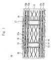
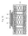
- FIG. 1is a sectional view showing the wiring substrate of the semiconductor device concerning Embodiment 1 of the present invention
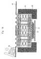
- FIG. 2is a top view showing the wiring substrate of the semiconductor device concerning Embodiment 1 of the present invention
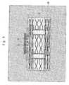
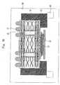
- FIG. 3is a bottom view showing the wiring substrate of the semiconductor device concerning Embodiment 1 of the present invention.
- FIG. 4is a side view of a semiconductor chip
- FIG. 5is a bottom view of a semiconductor chip
- FIG. 6is a sectional view showing the state where the semiconductor chip was located above wiring substrate 10 ;
- FIG. 7is a sectional view showing the state that the bump of a semiconductor chip and the bump of a wiring substrate are made to weld by pressure;
- FIG. 8is a top view showing the state where the flip chip bond of the semiconductor chip was made to the upper surface of the wiring substrate;
- FIG. 9is a sectional view showing the state that a wiring substrate and a semiconductor chip are exposed to O 2 plasma;
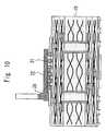
- FIG. 10is a sectional view showing the state that under-filling resin is poured into the gap of a semiconductor chip and a wiring substrate;
- FIG. 11is a sectional view showing the state that a wiring substrate and a semiconductor chip are put in a baking furnace, and baking is performed;
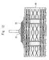
- FIG. 12is a sectional view showing the state that heat radiation resin is applied to the back surface of a semiconductor chip
- FIG. 13is a sectional view showing the state that a heat spreader is adhered on the back surface of a semiconductor chip
- FIG. 14is a sectional view showing the state that a wiring substrate, a semiconductor chip, and a heat spreader are put in a baking furnace, and baking is performed;
- FIG. 15is a top view showing the state where the heat spreader was mounted on the back surface of the semiconductor chip
- FIG. 16is a sectional view showing the state that the flux is applied to the under surface of a wiring substrate
- FIG. 17is a sectional view showing the state where the solder ball was located above the wiring substrate
- FIG. 18is a sectional view showing the state that the wiring substrate which carried solder ball 37 is put in a reflow furnace, and reflow is performed;
- FIG. 19is the bottom view of a wiring substrate on which the solder balls were adhered.
- FIG. 20is a sectional view showing the state where alignment of the solder ball was made on the test pin
- FIG. 21is a sectional view showing the semiconductor device concerning Embodiment 1 of the present invention.
- FIG. 22is a sectional view showing the semiconductor device concerning Embodiment 2 of the present invention.
- FIG. 23is a partially expanded cross-sectional view of a semiconductor chip.
- FIG. 1is a sectional view showing the wiring substrate of the semiconductor device concerning Embodiment 1 of the present invention
- FIG. 2is the top view
- FIG. 3is the bottom view.
- This wiring substrate 10puts build-up substrates 12 a and 12 b on the upper surface of core substrate 11 , puts build-up substrates 12 c and 12 d on the under surface, and is made to unify by thermo-compression using a vacuum press etc. However, in order to prevent a warp of wiring substrate 10 , the build-up substrate of the same number of sheets is bonded together to the upper and lower sides of core substrate 11 .
- core substrate 11 and build-up substrates 12 a - 12 dinclude a layer in which the glass cloth was impregnated with insulating resin to solidify into a plate, respectively.
- the textile fabrics which include long glass textiles, or the nonwoven fabric which includes short glass textilesis also good as a glass cloth.
- the cross which includes another insulating materials with high rigidity compared with insulating resin, for example, a carbon fiber etc., instead of a glass clothcan also be used.
- insulating resinfor example polysulfone, polyether sulfone, polyphenyl sulfone, polyphthalamide, polyamidoimide, polyketone, polyacetal, polyimide, polycarbonate, modified polyphenylene ether, polybutylene terephthalate, polyarylate, polysulfone, polyphenylene sulfide, polyetheretherketone, tetrafluoroethylene, epoxy, bismaleimide system resin, etc.
- polysulfonefor example polysulfone, polyether sulfone, polyphenyl sulfone, polyphthalamide, polyamidoimide, polyketone, polyacetal, polyimide, polycarbonate, modified polyphenylene ether, polybutylene terephthalate, polyarylate, polysulfone, polyphenylene sulfide, polyetheretherketone, tetrafluoroethylene, epoxy, bismaleimide system resin, etc.
- polysulfonefor example polys
- Through hole 13is formed in core substrate 11 by the drill.
- the diameter of through hole 13is 100-300 ⁇ m, and is 200 ⁇ m here.
- through hole via 14which includes Cu etc. is formed at the side wall of through hole 13 by plating etc.
- Wiring layer 15which includes Cu etc. is formed on the upper surface of core substrate 11 by an electroplating method, photo lithography, etc.
- wiring layer 16which includes Cu etc. is similarly formed on the under surface of core substrate 11 . This wiring layer 15 and wiring layer 16 are connected via through hole via 14 .
- Through hole 17is formed also in build-up substrates 12 a - 12 d , respectively.
- a diameter of through hole 17 of build-up substrates 12 a - 12 dis small compared with that of through hole 13 of core substrate 11 , is 30-100 ⁇ m concretely, and is 50 ⁇ m here.
- UV-YAG laser, carbon dioxide gas laser, excimer laser, a dry etching method using plasma, etc.can be used for formation of this through hole 17 .
- wiring layer 18which includes Cu etc., is respectively formed by an electroplating method, photo lithography, etc.
- through hole via 19is formed in through hole 17 by filling up with electric conduction paste, such as Cu.
- solder resist 20The front surface of wiring substrate 10 is covered by solder resist 20 . Opening is formed in this solder resist 20 , and a part of top and lowest wiring layer 18 is exposed.
- solder resist 20a resin which is electrically and thermally excellent, such as an epoxy system, a polyimide system, an acrylic system, and BT system, can be used.
- bump 21 awhich includes lead free solder is formed by plating or vacuum deposition on the exposed top wiring layer 18 .
- These bumps 21 aare arranged on wiring substrate 10 in a lattice manner.
- bumps 21 aare arranged at full matrix form in the region on which semiconductor chip 22 is arranged, various arrangement can be chosen suitably.
- Lead free solderis solder in which lead is not included or only lead of the grade (less than 1 wt %) with few environmental impacts is included.
- lead free solderis solder in which lead is not included or only lead of the grade (less than 1 wt %) with few environmental impacts is included.
- what contained Cu 1 to 3% in Snis used as lead free solder.
- FIG. 4is a side view of a semiconductor chip
- FIG. 5is the bottom view.
- Bumps 21 bwhich include lead free solder are formed on the mounting surface of semiconductor chip 22 by plating or vacuum deposition.
- the partially expanded cross-sectional view of semiconductor chip 22is described in FIG. 23 .
- Semiconductor chip 22is provided with silicon substrate 100 , semiconductor element 101 formed on silicon substrate 100 , such as MOSFET, an interlayer insulation film which includes a laminated structure of SiO 2 insulating film 102 , SiCN etching stopper film 103 , SiOC low dielectric constant film 104 , and SiOF tightly adhering film 105 , wiring layer 106 in a chip which includes a tungsten plug embedded in this interlayer insulation film, Cu wiring, etc., aluminum pad layer 107 formed on the interlayer insulation film, a laminated film of inorganic passivation film 108 which includes a SiO 2 /SiN laminated film, and organic passivation film 109 which includes a polyimide film (PiQ film) in which an opening was formed so that aluminum pad 107 might be exposed, barrier metal 110 which was formed on aluminum pad 107 and which includes, for example a Ti/Cu/Ni laminated film, and solder bump 21 b formed on barrier metal 110 .
- SiQ filmpolyimide film
- the strength reduction of the interlayer insulation filmposes a problem.
- the problemis remarkable in a porous Low-k film which reduces a dielectric constant by reducing the density of a film especially as compared with the TEOS film which is SiO 2 common film.
- the technology of reducing the stress applied to a chipbecomes very important, when improving the reliability of a semiconductor device.
- a porous SiOC filmis adopted as a low dielectric constant film.
- This porous SiOC filmis methyl-containing polysiloxane which mainly includes many Si—CH 3 groups, since a gap is generated in molecular structure by existence of CH 3 , it becomes porosity, and the dielectric constant is falling.
- a material which forms semiconductor chip 22although the example was shown above, it is not restricted to these.
- a porous low dielectric constant film of SiOCH baseporous silica system materials, such as a Nano Clustering Silica film, H-containing polysiloxane which is called porous HSQ, organic polymer film, and a porous film of organic polymer etc. are available suitably.
- wiring substrate 10is laid in the predetermined location on bonding stage 24 . And the surface on which bumps 21 b were formed is turned down, and vacuum adsorption of the semiconductor chip 22 is made on the under surface of bonding head 25 . And horizontal displacement of the bonding head 25 is made, and semiconductor chip 22 is located above wiring substrate 10 .
- bonding stage 24heats wiring substrate 10 to about 150° C. with the built-in heater (un-illustrating).
- bonding head 25heats semiconductor chip 22 to about 150° C. with the built-in heater (un-illustrating).
- bonding head 25is descended and bump 21 b of semiconductor chip 22 and bump 21 a of wiring substrate 10 are made to weld by pressure, as shown in FIG. 7 .
- semiconductor chip 22is heated to about 260° C. which is more than a solder melting point by bonding head 25 , and bonding head 25 is made to move (scrub) rhythmically periodically to a horizontal direction or a perpendicular direction, where bumps 21 a and 21 b are melted.
- bump 21 a and bump 21 bunify, and bump 21 is formed.
- FIG. 8is a top view showing the condition of having made the flip chip bond of the semiconductor chip to the upper surface of the wiring substrate.
- the flip chip bondcan be performed for semiconductor chip 22 to wiring substrate 10 via bump 21 according to the above-mentioned step, without using flux, the washing process of the flux can be skipped. Since void is not formed in bump 21 by expansion of a flux residue, reliability can be improved.
- wiring substrate 10 and semiconductor chip 22are exposed to O 2 plasma. Since this O 2 plasma also enters a slit compared with an argon spatter etc., O 2 plasma can be supplied also to the gap of semiconductor chip 22 and wiring substrate 10 .
- the passivation filmsfor example, organic resin films, such as a polyimide film
- the passivation filmsare cleaned and activated (roughened) by this plasma treatment.
- adhesion with the under-filling resin formed latercan be improved.
- the filling factor of under-filling resin in the gap of semiconductor chip 22 and wiring substrate 10can be improved.
- under-filling resin 28 of paste state or liquid stateis poured into the gap of semiconductor chip 22 and wiring substrate 10 .
- Thermosetting resinsuch as an epoxy resin, can be used as under-filling resin 28 , and a filler etc. may be contained.
- the under-filling resinwhose glass transition temperature (Tg) is 100-120° C., for example, 110° C., is used.
- Tgglass transition temperature
- DMA methodpulse method
- wiring substrate 10 and semiconductor chip 22are put in baking furnace 29 , and baking of about 6 hours is performed at about 125° C. which is low temperature from the former. This cures under-filling resin 28 .
- the modulus of elasticity of under-filling resinis securable by making Tg to more than or equal to 100° C. also at about 125° C.-150° C. which are generally asked for operational reliability. For this reason, a bump can fully be protected.
- Resin curing temperature(curing temperature) can be made low by making Tg less than or equal to 120° C. For this reason, after curing under-filling resin, the difference of temperature at the time of making it change from resin curing temperature to low temperature can be made small, and the internal stress applied to a chip can be made small.
- heat radiation resin 31is applied to the back surface of semiconductor chip 22 .
- heat spreader 32is adhered on the back surface of semiconductor chip 22 with heat radiation resin 31 .
- material of heat spreader 32Cu, Al, Al—Si—Cu alloy, etc. can be used in consideration of heat radiation property.
- the stiffeneris omitted for cost reduction, and the shape is made to have a clearance more than or equivalent to the thickness of the chip between the portion which projects to the perimeter of the chip of the heat spreader, and the wiring substrate upper surface, when heat radiation resin 31 is thin, a crack and a damage will enter into semiconductor chip 22 easily. On the other hand, when heat radiation resin 31 is thick, the divergence characteristics of heat will worsen. Therefore, it is necessary to control the thickness (gap) of heat radiation resin 31 with high precision.
- the size of the filler mixed in heat radiation resin 31is optimized, and the thickness of heat radiation resin 31 is controlled.
- the thing the average particle diameter of whose filler is 13 ⁇ mis used.
- the thing whose particle diameter is more than or equal to 45 ⁇ mis cut using a mesh.
- the thickness of heat radiation resinis controllable to 60 ⁇ 20 ⁇ m.
- a filleris chosen so that it may have the relation:
- the thickness of heat radiation resinis controllable within fixed limits centered on desired thickness.
- heat radiation resin 31it is preferred to use the heat-curing type heat radiation resin of a silicone system from the ease of workability and the height of the heat conductivity.
- Silicone system heat radiation resinis the resin which blended highly thermally conductive powders, such as alumina, with the base of silicone oil. Since it is a product of high viscosity grease state in the state before cure, the thickness of heat radiation resin 31 can be controlled comparatively easily and in quite high accuracy by using the position control of a jig.
- viscosity of heat radiation resin 31material higher than the viscosity at the time of injection of under-filling resin 28 is preferred at least.
- maximum grain size B MAX of a filleralthough not restricted to 4 ⁇ 5 or less of thickness A of heat radiation resin, it is preferred to have the relation that maximum grain size B MAX of a filler is smaller than the portion A MIN at which the thickness becomes the smallest of heat radiation resin.
- B MAXbecomes the same as A MIN , or larger than that, possibility that a filler will be put between heat spreader 32 and semiconductor chip 22 back surface will become high.
- Shape of a filleris made into a globular form and the damage to semiconductor chip 22 or heat spreader 32 is made small.
- the shape of a filleris not a globular form strictly, let the particle diameter of a filler be a diameter of the longest place.
- wiring substrate 10 , semiconductor chip 22 , and heat spreader 32are put in baking furnace 29 , baking is performed, and heat radiation resin 31 is cured. This mounts heat spreader 32 on semiconductor chip 22 .
- FIG. 15is a top view showing the state of having mounted heat spreader 32 on semiconductor chip 22 .
- Heat spreader 32is made small compared with wiring substrate 10 . Hereby, cost can be reduced. However, in order to secure heat radiation property, heat spreader 32 is made larger than semiconductor chip 22 .
- wiring substrate 10is turned down, and wiring substrate 10 is held by hold means 33 which touches the portion which is the upper surface (surface on which semiconductor chip 22 was mounted) of wiring substrate 10 and the outside of heat spreader 32 , and the side surface of wiring substrate 10 .
- hold means 33which touches the portion which is the upper surface (surface on which semiconductor chip 22 was mounted) of wiring substrate 10 and the outside of heat spreader 32 , and the side surface of wiring substrate 10 .
- wiring substrate 10can be held, without giving stress to semiconductor chip 22 and heat spreader 32 .
- flux 35is applied to the under surface of wiring substrate 10 via mask 34 .
- flux 35is applied to wiring layer 18 exposed on the under surface of wiring substrate 10 .
- soldering pastemay be applied instead of flux 35 .
- FIG. 18is a bottom view of the wiring substrate which joined the solder ball.
- solder ball 37 of wiring substrate 10is turned downward, and alignment of the solder ball 37 is made on test pin 41 which includes elastic members, such as a spring. And solder ball 37 of wiring substrate 10 is pushed against test pin 41 by pressing down wiring substrate 10 by pressing tool 42 from an upside.
- pressing tool 42has the space which includes heat spreader 32 and semiconductor chip 22 , and presses down the portion which is the upper surface of wiring substrate 10 and the outside of heat spreader 32 .
- the electric test of wiring substrate 10 and semiconductor chip 22is done by exchanging an electrical signal between test pin 41 and solder ball 37 in this state.
- the semiconductor device concerning Embodiment 1 of the present invention as shown in FIG. 21is completed. Then, the above-mentioned semiconductor device is mounted on a mother board etc. using solder balls 37 .
- This semiconductor deviceomits the stiffener conventionally formed in order to reinforce the wiring substrate and to maintain the surface smoothness of the heat spreader for cost reduction, and has the shape which has a clearance more than or equivalent to the thickness of the chip between most portions which project to the perimeter of the chip of the heat spreader, and the wiring substrate upper surface.
- under-filling resin 28it may become the shape which fills between the very portion which projects to the perimeter of the chip of the heat spreader and the wiring substrate upper surface, but as compared with the case where it has a stiffener, the effect of reinforcement of a wiring substrate is very restrictive.
- the rigidity improvement in the wiring substrate itselfbecomes important.
- a glass clothis contained not only core substrate 11 but build-up substrate 12 a - 12 d.
- wiring substrate 10has a plurality of insulating substrates (core substrate 11 and build-up substrates 12 a - 12 d ) in which a through hole whose diameter differs, respectively was formed, and each insulating substrate contains a glass cloth.
- Wiring substrate 10has the insulating substrate (build-up substrates 12 a - 12 d ) in which a through hole whose diameter is 100 ⁇ m or less was formed, and this insulating substrate also contains a glass cloth.
- the thickness of the glass cloth which build-up substrate 12 a - 12 d containsis made thinner than the thickness of the glass cloth which core substrate 11 contains.
- the thickness of build-up substrates 12 a - 12 dis also made thinner than core substrate 11 .
- organic system passivation filmssuch as a polyimide passivation film
- organic system passivation filmshave high adhesion with under-filling resin 28 as compared with inorganic system passivation films, such as a SiN film.
- wiring substrate 10the case where what has high rigidity by containing a glass cloth in each layer was used was described as wiring substrate 10 .
- the method of using the glass cloth which wove the glass fiber in the shape of a clothbut also the method of using the nonwoven fabric type glass cloth formed by the glass fiber, the method of making the short glass fiber be contained as a reinforcement agent, etc. can be chosen suitably.
- material of the fibernot only the glass that uses silica as a base but the material which uses a carbon fiber can be chosen suitably.
- FIG. 22is a sectional view showing the semiconductor device concerning Embodiment 2 of the present invention.
- the difference with Embodiment 1is using the thing which made thin insulating substrates 43 a - 43 d in which the through hole less than or equal to 100 ⁇ m was formed for the diameter bond by thermo-compression with a vacuum press etc., and made them unify, not using a core substrate as wiring substrate 10 .
- each insulating substrates 43 a - 43 dinclude the layer in which the glass cloth was impregnated with insulating resin, respectively, and was solidified platy.
- Other structureis the same as that of Embodiment 1.
- Embodiment 3heat radiation property is improved using the thing smaller than Embodiment 1 as a filler mixed in heat radiation resin 31 .
- the fillerwhose average particle diameter is 5.8 ⁇ m and whose maximum grain size is 24 ⁇ m is used.
- a spacer which includes globular form zirconiais mixed in heat radiation resin 31 .
- the spacer whose average particle diameter is 25 ⁇ m and whose maximum grain size is 33 ⁇ mis used.
- the thickness of heat radiation resin 31is controllable by this spacer to 60 ⁇ 20 ⁇ m.
- the desired thickness of heat radiation resinis set to A
- average particle diameter of a spaceris set to C
- a spaceris chosen so that it may have the relation:
- the thickness of heat radiation resinis controllable within fixed limits centered on desired thickness.
- a spaceris chosen so that it may have the relation:
- the thickness of heat radiation resinis controllable by not a filler but a spacer.
- Average particle diameter of a filleris set to B, the minimum particle size of a spacer is set to C MIN , the particle diameter which occupies 90% of the occupying rate of a filler is made into B 90% , and a spacer is chosen so that it may have any of relations:
- the content in heat radiation resin of a spaceris made to less than or equal to 10 volume %, and preferably to less than or equal to 5 volume %.
- the flow property of heat radiation resin 31 which adheres semiconductor chip 22 and heat spreader 32is set as the following values.
- the flow property of heat radiation resin 31shall be decided by making 1 g heat radiation resin dropped on a plane from the 10 mm upper part at room-temperature 25° C., and measuring the breadth of the heat radiation resin.
- the heat radiation resin of the flow property whose breadth is 4 mm or more, and 12 mm or less, for example, 8 mmis used in the above-mentioned measuring method.
- a drift of heat spreader 32can be prevented by using the heat radiation resin of flow property whose breadth is 12 mm or less. Since it fully gets wet and spreads when heat radiation resin 31 is applied on semiconductor chip 22 by using the heat radiation resin of flow property whose breadth is 4 mm or more, the generation of void can be prevented.
Landscapes
- Engineering & Computer Science (AREA)
- Microelectronics & Electronic Packaging (AREA)
- Computer Hardware Design (AREA)
- Power Engineering (AREA)
- Physics & Mathematics (AREA)
- Condensed Matter Physics & Semiconductors (AREA)
- General Physics & Mathematics (AREA)
- Manufacturing & Machinery (AREA)
- Chemical & Material Sciences (AREA)
- Materials Engineering (AREA)
- Ceramic Engineering (AREA)
- Geometry (AREA)
- Wire Bonding (AREA)
- Structures For Mounting Electric Components On Printed Circuit Boards (AREA)
- Cooling Or The Like Of Semiconductors Or Solid State Devices (AREA)
- Production Of Multi-Layered Print Wiring Board (AREA)
Abstract
Description
- This application is a Continuation of U.S. Ser. No. 15/796,746 filed Oct. 27, 2017, which is a Continuation of U.S. Ser. No. 15/398,444 filed Jan. 4, 2017, now U.S. Pat. No. 9,831,166, which is a Continuation of U.S. Ser. No. 15/241,777 filed Aug. 19, 2016, now U.S. Pat. No. 9,576,890, which is a Continuation of U.S. Ser. No. 15/045,978 filed Feb. 17, 2016, now U.S. Pat. No. 9,496,153, which is a continuation of U.S. Ser. No. 14/569,423 filed Dec. 12, 2014, now U.S. Pat. No. 9,299,681, which is a Continuation Application of U.S. Ser. No. 14/338,175 filed Jul. 22, 2014, now U.S. Pat. No. 8,928,147, which is a Continuation of U.S. Ser. No. 14/044,497 filed Oct. 2, 2013, now U.S. Pat. No. 8,822,269, which is a Divisional of U.S. Ser. No. 13/863,241 filed Apr. 15, 2013, now U.S. Pat. No. 8,581,410, which is a Continuation of U.S. Ser. No. 13/648,876 filed Oct. 10, 2012, now U.S. Pat. No. 8,575,757, which is a Continuation of U.S. Ser. No. 13/367,029 filed Feb. 6, 2012, now U.S. Pat. No. 8,314,495, which is a Continuation of U.S. Ser. No. 13/183,196 filed Jul. 14, 2011, now Abandoned, which is a Divisional of U.S. Ser. No. 12/753,521 filed Apr. 2, 2010, now U.S. Pat. No. 8,018,066, which is a Divisional of U.S. Ser. No. 12/401,193 filed Mar. 10, 2009, now U.S. Pat. No. 7,791,204, which is a Divisional of U.S. Ser. No. 11/406,337 filed Apr. 19, 2006, now U.S. Pat. No. 7,521,799, which claims priority from Japanese patent applications No. 2005-121063 filed on Apr. 19, 2005, and No. 2006-096999 filed on Mar. 31, 2006. The subject matter of each is incorporated herein by reference in entirety.
- The present invention relates to a semiconductor device which makes flip chip connection of a semiconductor chip on a wiring substrate, and forms a heat spreader on a back surface of this semiconductor chip, and its manufacturing method.
- A semiconductor device which makes flip chip connection of the semiconductor chip via the bump on the wiring substrate is proposed. The gap of the semiconductor chip and the wiring substrate is filled up with under-filling resin in this semiconductor device. In order to make heat radiation property high, a heat spreader is formed on the back surface of the semiconductor chip. In order to reinforce a wiring substrate and to maintain the surface smoothness of a heat spreader conventionally, a stiffener (reinforcing plate) was formed (for example, refer to Patent Reference 1).
- What formed the build-up substrate by soft resin coating or a soft film being conventionally stuck on both sides of the hard core substrate containing a glass cloth was used as a wiring substrate. And wirings of fine pitch were formed in the build-up substrate. However, since the build-up substrate was soft, the rigidity of the wiring substrate itself was not high.
- [Patent Reference 1] Japanese Unexamined Patent Publication No. 2003-51568
- Since a conventional wiring substrate does not have high rigidity as mentioned above, when the stiffener is omitted for cost reduction, and the shape is made to have a clearance between the portion which projects to the perimeter of the chip of the heat spreader, and the wiring substrate upper surface, the wiring substrate of the portion which projects to the perimeter of the chip becomes the shape where, although a very portion is covered by under-filling resin, the most exposes, and twist and distortion of the wiring substrate generate. Hereby, there were problems that the solder ball joined to the under surface of the wiring substrate floated, or a stress was applied to the edge of the semiconductor chip.
- There was a problem that the adhesion of a semiconductor chip, a wiring substrate, and under-filling may not be good, and the gap of the semiconductor chip and the wiring substrate was not fully filled up with under-filling resin. And in an argon spatter, argon etc. could not fully be supplied to the narrow gap of the semiconductor chip and the wiring substrate, and the adhesion of the gap concerned has not fully been improved.
- When the stiffener is omitted for cost reduction, the shape is made to have a clearance between the portion which projects to the perimeter of the chip of the heat spreader, and the wiring substrate upper surface, and heat radiation resin is thin, a crack and a damage will enter into the semiconductor chip easily. On the other hand, when heat radiation resin is thick, the divergence characteristics of heat will worsen. Therefore, it is necessary to control the thickness of heat radiation resin with high precision.
- In the case that the stiffener is omitted, and the shape is made to have a clearance between the portion which projects to the perimeter of the chip of the heat spreader, and the wiring substrate upper surface, when a solder ball is formed on the under surface of the wiring substrate, and doing an electric test of the wiring substrate and the semiconductor chip after that, there was also a problem of the heat spreader having hit a formation instrument and a test instrument, and damaging.
- The present invention was made in order to solve the above problems. The first purpose is to obtain a semiconductor device which can prevent the generation of twist and distortion of a wiring substrate, even when the stiffener is omitted.
- The second purpose is to obtain a manufacturing method of a semiconductor device which can improve the filling factor of the under-filling resin in the gap of a semiconductor chip and a wiring substrate.
- The third purpose is to obtain a semiconductor device which can control the thickness of heat radiation resin with high precision, when the shape is made to omit the stiffener and to have a clearance between the portion which projects to the perimeter of the chip of the heat spreader, and the wiring substrate upper surface.
- The fourth purpose is to obtain a manufacturing method of a semiconductor device which can prevent a heat spreader's hitting a formation instrument and a test instrument, and damaging in the case of formation of a solder ball, or an electric test, even when the shape is made to omit the stiffener and to have a clearance between the portion which projects to the perimeter of the chip of the heat spreader, and the wiring substrate upper surface.
- The semiconductor device according to one aspect of the present disclosure comprises: a wiring substrate; a semiconductor chip which is flip-chip-bonded over the wiring substrate; and a heat spreader adhered over a back surface of the semiconductor chip; wherein a stiffener for reinforcing the wiring substrate and maintaining a surface smoothness of the heat spreader is omitted; and the wiring substrate has a plurality of insulating substrates in which a through hole whose diameter differs, respectively is formed, and each insulating substrate contains a glass cloth.
- The semiconductor device according to another aspect of the present disclosure comprises: a wiring substrate; a semiconductor chip which is flip-chip-bonded over the wiring substrate; and a heat spreader adhered over a back surface of the semiconductor chip; wherein a stiffener for reinforcing the wiring substrate and maintaining a surface smoothness of the heat spreader is omitted; and the wiring substrate has a plurality of layers of insulating substrates in which a through hole whose diameter is less than 100 μm is formed, and a plurality of layers of wiring layers, and the insulating substrate contains a glass cloth.
- The method of manufacturing a semiconductor device comprises the steps of: flip-chip-bonding a semiconductor chip via a bump over a wiring substrate; supplying O2plasma in a gap of the wiring substrate and the semiconductor chip after the step of flip-chip-bonding; and pouring under-filling resin in the gap of the wiring substrate and the semiconductor chip after the step of supplying O2plasma.
- The semiconductor device according to another aspect of the present disclosure comprises: a wiring substrate; a semiconductor chip flip-chip-bonded over the wiring substrate; and a heat spreader adhered over a back surface of the semiconductor chip with heat radiation resin; wherein the heat radiation resin contains a filler; and by setting a thickness of the heat radiation resin to A, and a maximum grain size of the filler to BMAX, a relation: A×4/5≥BMAXis held.
- The semiconductor device comprises: a wiring substrate; a semiconductor chip flip-chip-bonded over the wiring substrate; and a heat spreader adhered over a back surface of the semiconductor chip with heat radiation resin; wherein the heat radiation resin contains a filler and a spacer; and by setting a thickness of the heat radiation resin to A, and an average particle diameter of the spacer to C, a relation of A×9/10≥C is held.
- The method of manufacturing a semiconductor device concerning claim11 of the present invention comprises the steps of: flip-chip-bonding a semiconductor chip over an upper surface of a wiring substrate; adhering a heat spreader smaller than the wiring substrate over a back surface of the semiconductor chip; holding the wiring substrate by a hold means which touches a portion which is an upper surface of the wiring substrate and an outside of the heat spreader, turning the upper surface of the wiring substrate down; and joining a solder bump to an under surface of the wiring substrate where the wiring substrate is held. The other features of the present invention are made clear to below.
- Even when the shape is made to have a clearance between the portion which projects to the perimeter of the chip of the heat spreader, and the wiring substrate upper surface, the generation of twist and distortion of the wiring substrate can be prevented.
- The present invention, the filling factor of the under-filling resin in the gap of a semiconductor chip and a wiring substrate can be improved.
- Even when the shape is made to have a clearance between the portion which projects to the perimeter of the chip of the heat spreader, and the wiring substrate upper surface, the thickness of heat radiation resin can be controlled with high precision.
- Even when the shape is made to have a clearance between the portion which projects to the perimeter of the chip of the heat spreader, and the wiring substrate upper surface, a heat spreader's hitting a formation instrument and a test instrument, and damaging can be prevented in the case of formation of a solder ball.
FIG. 1 is a sectional view showing the wiring substrate of the semiconductor device concerning Embodiment 1 of the present invention;FIG. 2 is a top view showing the wiring substrate of the semiconductor device concerning Embodiment 1 of the present invention;FIG. 3 is a bottom view showing the wiring substrate of the semiconductor device concerning Embodiment 1 of the present invention;FIG. 4 is a side view of a semiconductor chip;FIG. 5 is a bottom view of a semiconductor chip;FIG. 6 is a sectional view showing the state where the semiconductor chip was located above wiring substrate10;FIG. 7 is a sectional view showing the state that the bump of a semiconductor chip and the bump of a wiring substrate are made to weld by pressure;FIG. 8 is a top view showing the state where the flip chip bond of the semiconductor chip was made to the upper surface of the wiring substrate;FIG. 9 is a sectional view showing the state that a wiring substrate and a semiconductor chip are exposed to O2plasma;FIG. 10 is a sectional view showing the state that under-filling resin is poured into the gap of a semiconductor chip and a wiring substrate;FIG. 11 is a sectional view showing the state that a wiring substrate and a semiconductor chip are put in a baking furnace, and baking is performed;FIG. 12 is a sectional view showing the state that heat radiation resin is applied to the back surface of a semiconductor chip;FIG. 13 is a sectional view showing the state that a heat spreader is adhered on the back surface of a semiconductor chip;FIG. 14 is a sectional view showing the state that a wiring substrate, a semiconductor chip, and a heat spreader are put in a baking furnace, and baking is performed;FIG. 15 is a top view showing the state where the heat spreader was mounted on the back surface of the semiconductor chip;FIG. 16 is a sectional view showing the state that the flux is applied to the under surface of a wiring substrate;FIG. 17 is a sectional view showing the state where the solder ball was located above the wiring substrate;FIG. 18 is a sectional view showing the state that the wiring substrate which carried solder ball37 is put in a reflow furnace, and reflow is performed;FIG. 19 is the bottom view of a wiring substrate on which the solder balls were adhered;FIG. 20 is a sectional view showing the state where alignment of the solder ball was made on the test pin;FIG. 21 is a sectional view showing the semiconductor device concerning Embodiment 1 of the present invention;FIG. 22 is a sectional view showing the semiconductor device concerning Embodiment 2 of the present invention; and.FIG. 23 is a partially expanded cross-sectional view of a semiconductor chip.- Hereafter, the manufacturing method of the semiconductor device concerning Embodiment 1 of the present invention is explained using drawings.
FIG. 1 is a sectional view showing the wiring substrate of the semiconductor device concerning Embodiment 1 of the present invention,FIG. 2 is the top view, andFIG. 3 is the bottom view.- This wiring substrate10 puts build-up substrates12aand12bon the upper surface of core substrate11, puts build-up substrates12cand12don the under surface, and is made to unify by thermo-compression using a vacuum press etc. However, in order to prevent a warp of wiring substrate10, the build-up substrate of the same number of sheets is bonded together to the upper and lower sides of core substrate11.
- And core substrate11 and build-up substrates12a-12dinclude a layer in which the glass cloth was impregnated with insulating resin to solidify into a plate, respectively. Here, the textile fabrics which include long glass textiles, or the nonwoven fabric which includes short glass textiles is also good as a glass cloth. And the cross which includes another insulating materials with high rigidity compared with insulating resin, for example, a carbon fiber etc., instead of a glass cloth can also be used.
- As insulating resin, for example polysulfone, polyether sulfone, polyphenyl sulfone, polyphthalamide, polyamidoimide, polyketone, polyacetal, polyimide, polycarbonate, modified polyphenylene ether, polybutylene terephthalate, polyarylate, polysulfone, polyphenylene sulfide, polyetheretherketone, tetrafluoroethylene, epoxy, bismaleimide system resin, etc. can be used.
- Through hole13 is formed in core substrate11 by the drill. The diameter of through hole13 is 100-300 μm, and is 200 μm here. And through hole via14 which includes Cu etc. is formed at the side wall of through hole13 by plating etc. Wiring layer15 which includes Cu etc. is formed on the upper surface of core substrate11 by an electroplating method, photo lithography, etc. And wiring layer16 which includes Cu etc. is similarly formed on the under surface of core substrate11. This wiring layer15 and wiring layer16 are connected via through hole via14.
- Through hole17 is formed also in build-up substrates12a-12d, respectively. However, since build-up substrates12a-12dare thin compared with core substrate11, and fine processing is easy for them, a diameter of through hole17 of build-up substrates12a-12dis small compared with that of through hole13 of core substrate11, is 30-100 μm concretely, and is 50 μm here. UV-YAG laser, carbon dioxide gas laser, excimer laser, a dry etching method using plasma, etc. can be used for formation of this through hole17.
- On build-up substrate12a-12d, wiring layer18 which includes Cu etc., is respectively formed by an electroplating method, photo lithography, etc. And through hole via19 is formed in through hole17 by filling up with electric conduction paste, such as Cu.
- The front surface of wiring substrate10 is covered by solder resist20. Opening is formed in this solder resist20, and a part of top and lowest wiring layer18 is exposed. As solder resist20, a resin which is electrically and thermally excellent, such as an epoxy system, a polyimide system, an acrylic system, and BT system, can be used.
- And bump21awhich includes lead free solder is formed by plating or vacuum deposition on the exposed top wiring layer18. These bumps21aare arranged on wiring substrate10 in a lattice manner. In
FIG. 2 , although bumps21aare arranged at full matrix form in the region on which semiconductor chip22 is arranged, various arrangement can be chosen suitably. Lead free solder is solder in which lead is not included or only lead of the grade (less than 1 wt %) with few environmental impacts is included. Here, what contained Cu 1 to 3% in Sn is used as lead free solder. FIG. 4 is a side view of a semiconductor chip, andFIG. 5 is the bottom view. Bumps21bwhich include lead free solder are formed on the mounting surface of semiconductor chip22 by plating or vacuum deposition. The partially expanded cross-sectional view of semiconductor chip22 is described inFIG. 23 . Semiconductor chip22 is provided with silicon substrate100, semiconductor element101 formed on silicon substrate100, such as MOSFET, an interlayer insulation film which includes a laminated structure of SiO2insulating film102, SiCN etching stopper film103, SiOC low dielectric constant film104, and SiOF tightly adhering film105, wiring layer106 in a chip which includes a tungsten plug embedded in this interlayer insulation film, Cu wiring, etc., aluminum pad layer107 formed on the interlayer insulation film, a laminated film of inorganic passivation film108 which includes a SiO2/SiN laminated film, and organic passivation film109 which includes a polyimide film (PiQ film) in which an opening was formed so that aluminum pad107 might be exposed, barrier metal110 which was formed on aluminum pad107 and which includes, for example a Ti/Cu/Ni laminated film, and solder bump21bformed on barrier metal110. When using a film of a dielectric constant lower than the dielectric-constant of SiO2film K=4.3 as an interlayer insulation film in semiconductor chip22, the strength reduction of the interlayer insulation film poses a problem. The problem is remarkable in a porous Low-k film which reduces a dielectric constant by reducing the density of a film especially as compared with the TEOS film which is SiO2common film. The technology of reducing the stress applied to a chip becomes very important, when improving the reliability of a semiconductor device. In this embodiment, a porous SiOC film is adopted as a low dielectric constant film. This porous SiOC film is methyl-containing polysiloxane which mainly includes many Si—CH3groups, since a gap is generated in molecular structure by existence of CH3, it becomes porosity, and the dielectric constant is falling. As a material which forms semiconductor chip22, although the example was shown above, it is not restricted to these. For example, as a low dielectric constant film, a porous low dielectric constant film of SiOCH base, porous silica system materials, such as a Nano Clustering Silica film, H-containing polysiloxane which is called porous HSQ, organic polymer film, and a porous film of organic polymer etc. are available suitably.- Next, the step which performs flip chip bond of the semiconductor chip22 on the above-mentioned wiring substrate10 is explained.
- First, as shown in
FIG. 6 , wiring substrate10 is laid in the predetermined location on bonding stage24. And the surface on which bumps21bwere formed is turned down, and vacuum adsorption of the semiconductor chip22 is made on the under surface of bonding head25. And horizontal displacement of the bonding head25 is made, and semiconductor chip22 is located above wiring substrate10. - On this occasion, bonding stage24 heats wiring substrate10 to about 150° C. with the built-in heater (un-illustrating). Similarly, bonding head25 heats semiconductor chip22 to about 150° C. with the built-in heater (un-illustrating).
- Next, bonding head25 is descended and bump21bof semiconductor chip22 and bump21aof wiring substrate10 are made to weld by pressure, as shown in
FIG. 7 . In this condition, semiconductor chip22 is heated to about 260° C. which is more than a solder melting point by bonding head25, and bonding head25 is made to move (scrub) rhythmically periodically to a horizontal direction or a perpendicular direction, where bumps21aand21bare melted. As a result, bump21aand bump21bunify, and bump21 is formed. - Then, bonding head25 is cooled to temperature lower than a solder melting point, and bump21 is solidified. And adsorption of semiconductor chip22 by bonding head25 is canceled, bonding head25 is raised, and bonding is terminated.
FIG. 8 is a top view showing the condition of having made the flip chip bond of the semiconductor chip to the upper surface of the wiring substrate. - Since the flip chip bond can be performed for semiconductor chip22 to wiring substrate10 via bump21 according to the above-mentioned step, without using flux, the washing process of the flux can be skipped. Since void is not formed in bump21 by expansion of a flux residue, reliability can be improved.
- Next, the step which forms under-filling resin between semiconductor chip22 and wiring substrate10 in order to prevent that bump21 is injured with thermal stress etc. is explained.
- First, as shown in
FIG. 9 , wiring substrate10 and semiconductor chip22 are exposed to O2plasma. Since this O2plasma also enters a slit compared with an argon spatter etc., O2plasma can be supplied also to the gap of semiconductor chip22 and wiring substrate10. - The passivation films (for example, organic resin films, such as a polyimide film) of wiring substrate10 and semiconductor chip22 are cleaned and activated (roughened) by this plasma treatment. Hereby, adhesion with the under-filling resin formed later can be improved. The filling factor of under-filling resin in the gap of semiconductor chip22 and wiring substrate10 can be improved.
- Next, as shown in
FIG. 10 , under-filling resin28 of paste state or liquid state is poured into the gap of semiconductor chip22 and wiring substrate10. Thermosetting resin, such as an epoxy resin, can be used as under-filling resin28, and a filler etc. may be contained. - Here, the under-filling resin whose glass transition temperature (Tg) is 100-120° C., for example, 110° C., is used. However, although there are various measuring methods of Tg, the DMA method (pull method) is used here.
- Next, as shown in
FIG. 11 , wiring substrate10 and semiconductor chip22 are put in baking furnace29, and baking of about 6 hours is performed at about 125° C. which is low temperature from the former. This cures under-filling resin28. - Thus, the modulus of elasticity of under-filling resin is securable by making Tg to more than or equal to 100° C. also at about 125° C.-150° C. which are generally asked for operational reliability. For this reason, a bump can fully be protected.
- Resin curing temperature (curing temperature) can be made low by making Tg less than or equal to 120° C. For this reason, after curing under-filling resin, the difference of temperature at the time of making it change from resin curing temperature to low temperature can be made small, and the internal stress applied to a chip can be made small.
- Next, the step which adheres a heat spreader on the back surface (the surface of the opposite side to the mounting surface) of semiconductor chip22 is explained.
- First, as shown in
FIG. 12 , heat radiation resin31 is applied to the back surface of semiconductor chip22. Next, as shown inFIG. 13 , heat spreader32 is adhered on the back surface of semiconductor chip22 with heat radiation resin31. As material of heat spreader32, Cu, Al, Al—Si—Cu alloy, etc. can be used in consideration of heat radiation property. - Since the stiffener is omitted for cost reduction, and the shape is made to have a clearance more than or equivalent to the thickness of the chip between the portion which projects to the perimeter of the chip of the heat spreader, and the wiring substrate upper surface, when heat radiation resin31 is thin, a crack and a damage will enter into semiconductor chip22 easily. On the other hand, when heat radiation resin31 is thick, the divergence characteristics of heat will worsen. Therefore, it is necessary to control the thickness (gap) of heat radiation resin31 with high precision.
- Then, the size of the filler mixed in heat radiation resin31 is optimized, and the thickness of heat radiation resin31 is controlled. Here, the thing the average particle diameter of whose filler is 13 μm is used. However, since the size of a filler has a distribution, the thing whose particle diameter is more than or equal to 45 μm is cut using a mesh. Hereby, the thickness of heat radiation resin is controllable to 60±20 μm.
- Namely, by setting the desired thickness of heat radiation resin to A, and the maximum grain size of a filler to BMAX, a filler is chosen so that it may have the relation:
A×4/5≥BMAX.- Hereby, the thickness of heat radiation resin is controllable within fixed limits centered on desired thickness. As heat radiation resin31, it is preferred to use the heat-curing type heat radiation resin of a silicone system from the ease of workability and the height of the heat conductivity. Silicone system heat radiation resin is the resin which blended highly thermally conductive powders, such as alumina, with the base of silicone oil. Since it is a product of high viscosity grease state in the state before cure, the thickness of heat radiation resin31 can be controlled comparatively easily and in quite high accuracy by using the position control of a jig. As viscosity of heat radiation resin31, material higher than the viscosity at the time of injection of under-filling resin28 is preferred at least. As maximum grain size BMAXof a filler, although not restricted to ⅘ or less of thickness A of heat radiation resin, it is preferred to have the relation that maximum grain size BMAXof a filler is smaller than the portion AMINat which the thickness becomes the smallest of heat radiation resin. When BMAXbecomes the same as AMIN, or larger than that, possibility that a filler will be put between heat spreader32 and semiconductor chip22 back surface will become high. Especially when it does not have the structure which supports heat spreaders32, such as a stiffener, firmly around semiconductor chip22 like this embodiment, in the step which sticks a heat spreader, when it is going to control the thickness of heat radiation resin only by load control, by the filler inserted between heat spreader32 and semiconductor chip22, a crack may enter into semiconductor chip22 back surface, and the reliability of the semiconductor device may be dropped.
- Shape of a filler is made into a globular form and the damage to semiconductor chip22 or heat spreader32 is made small. Here, when the shape of a filler is not a globular form strictly, let the particle diameter of a filler be a diameter of the longest place.
- Next, as shown in
FIG. 14 , wiring substrate10, semiconductor chip22, and heat spreader32 are put in baking furnace29, baking is performed, and heat radiation resin31 is cured. This mounts heat spreader32 on semiconductor chip22. FIG. 15 is a top view showing the state of having mounted heat spreader32 on semiconductor chip22. Heat spreader32 is made small compared with wiring substrate10. Hereby, cost can be reduced. However, in order to secure heat radiation property, heat spreader32 is made larger than semiconductor chip22.- Next, the step which joins the solder ball used as an external connection terminal to the under surface of wiring substrate10 is explained.
- First, as shown in
FIG. 16 , the upper surface of wiring substrate10 is turned down, and wiring substrate10 is held by hold means33 which touches the portion which is the upper surface (surface on which semiconductor chip22 was mounted) of wiring substrate10 and the outside of heat spreader32, and the side surface of wiring substrate10. Hereby, wiring substrate10 can be held, without giving stress to semiconductor chip22 and heat spreader32. - And where wiring substrate10 is held, flux35 is applied to the under surface of wiring substrate10 via mask34. Hereby, flux35 is applied to wiring layer18 exposed on the under surface of wiring substrate10. However, soldering paste may be applied instead of flux35.
- Next, as shown in
FIG. 17 , vacuum adsorption of the solder ball37 which includes lead free solder is made to the under surface of ball mounting head36. And horizontal displacement of the ball mounting head36 is made, and solder ball37 is located above wiring substrate10. And ball mounting head36 is descended and solder ball37 is mounted on flux35 of wiring substrate10. Then, adsorption of solder ball37 by ball mounting head36 is canceled, and ball mounting head36 is raised. - Next, as shown in
FIG. 18 , where wiring substrate10 is held by hold means33 turning solder ball37 upwards, putting on conveyor38, putting in reflow furnace39, reflow is performed, and solder ball37 is joined to wiring substrate10. Then, flux35 is removed by washing.FIG. 19 is a bottom view of the wiring substrate which joined the solder ball. - Next, as shown in
FIG. 20 , the surface which joined solder ball37 of wiring substrate10 is turned downward, and alignment of the solder ball37 is made on test pin41 which includes elastic members, such as a spring. And solder ball37 of wiring substrate10 is pushed against test pin41 by pressing down wiring substrate10 by pressing tool42 from an upside. However, pressing tool42 has the space which includes heat spreader32 and semiconductor chip22, and presses down the portion which is the upper surface of wiring substrate10 and the outside of heat spreader32. - The electric test of wiring substrate10 and semiconductor chip22 is done by exchanging an electrical signal between test pin41 and solder ball37 in this state.
- According to the above steps, the semiconductor device concerning Embodiment 1 of the present invention as shown in
FIG. 21 is completed. Then, the above-mentioned semiconductor device is mounted on a mother board etc. using solder balls37. - This semiconductor device omits the stiffener conventionally formed in order to reinforce the wiring substrate and to maintain the surface smoothness of the heat spreader for cost reduction, and has the shape which has a clearance more than or equivalent to the thickness of the chip between most portions which project to the perimeter of the chip of the heat spreader, and the wiring substrate upper surface. When there is much amount of under-filling resin28, it may become the shape which fills between the very portion which projects to the perimeter of the chip of the heat spreader and the wiring substrate upper surface, but as compared with the case where it has a stiffener, the effect of reinforcement of a wiring substrate is very restrictive. Thus, in the shape which the great portion of wiring substrate upper surface of the perimeter of the chip exposes, the rigidity improvement in the wiring substrate itself becomes important. And in wiring substrate10, a glass cloth is contained not only core substrate11 but build-up substrate12a-12d.
- That is, wiring substrate10 has a plurality of insulating substrates (core substrate11 and build-up substrates12a-12d) in which a through hole whose diameter differs, respectively was formed, and each insulating substrate contains a glass cloth. Wiring substrate10 has the insulating substrate (build-up substrates12a-12d) in which a through hole whose diameter is 100 μm or less was formed, and this insulating substrate also contains a glass cloth.
- Hereby, rigidity can be made high as the wiring substrate10 whole. Therefore, even when a stiffener is omitted for cost reduction, a warp and a distortion of wiring substrate10 can be prevented. As compared with core substrate11, formation of a finer through hole is required to the insulating layer which forms build-up substrates12a-12d. By making the diameter of a through hole small, the area of the portion which can arrange a wiring becomes wide and the degree of freedom of a wiring layout improves. In particular, when there are many electrodes formed on semiconductor chip22 as hundreds of or more pieces, i.e., the number of bumps21, securing the layout degree of freedom of wiring layer18 of the top layer which connects with bump21 becomes important. So, securing the forming accuracy in a micro fabrication becomes indispensable at build-up substrate12bwith which through hole via19 connected to wiring layer18 of the top layer is formed in the inside. In this embodiment, in order to secure the forming accuracy of build-up substrates12a-12d, the thickness of the glass cloth which build-up substrate12a-12dcontains is made thinner than the thickness of the glass cloth which core substrate11 contains. The thickness of build-up substrates12a-12dis also made thinner than core substrate11. Thus, by using a thin glass cloth as compared with that of core substrate11, and making thin build-up substrate12a-12deach layer, forming accuracy is improved maintaining the rigidity of build-up substrates12a-12d, and formation of fine through hole17 is made easy. When using, for example what has a vulnerable porous low dielectric constant film etc. as compared with a TEOS film instead of conventional SiO2interlayer insulation film as semiconductor chip22 like a description in this embodiment, to adopt build-up substrates12a-12dwhich increased strength by the glass cloth is especially effective. That is, by increasing the strength of build-up substrates12a-12d, the internal stress exerted on semiconductor chip22 can be reduced, and the generation of peeling in the vulnerable layer of semiconductor chip22 inside can be prevented. It is preferred as semiconductor chip22 that organic system passivation films, such as a polyimide passivation film, are formed on the main surface. Organic system passivation films, such as polyimide, have high adhesion with under-filling resin28 as compared with inorganic system passivation films, such as a SiN film. By covering main surface upper part of semiconductor chip22 by an organic system passivation film, peeling at the interface of under-filling resin28 and semiconductor chip22 can be prevented. By maintaining the almost equal adhesion state of the interface of under-filling resin28 and semiconductor chip22, the generation of problems, such as peeling inside the low dielectric constant film by a local stress concentration, can be prevented. In this embodiment, the case where what has high rigidity by containing a glass cloth in each layer was used was described as wiring substrate10. However, as a means which improves the rigidity of each layer of a wiring substrate, not only limited to the method of using the glass cloth which wove the glass fiber in the shape of a cloth, but also the method of using the nonwoven fabric type glass cloth formed by the glass fiber, the method of making the short glass fiber be contained as a reinforcement agent, etc. can be chosen suitably. Also as material of the fiber, not only the glass that uses silica as a base but the material which uses a carbon fiber can be chosen suitably.
FIG. 22 is a sectional view showing the semiconductor device concerning Embodiment 2 of the present invention. The difference with Embodiment 1 is using the thing which made thin insulating substrates43a-43din which the through hole less than or equal to 100 μm was formed for the diameter bond by thermo-compression with a vacuum press etc., and made them unify, not using a core substrate as wiring substrate10. However, each insulating substrates43a-43dinclude the layer in which the glass cloth was impregnated with insulating resin, respectively, and was solidified platy. Other structure is the same as that of Embodiment 1.- Hereby, rigidity can be made high as the wiring substrate10 whole. Therefore, even when the stiffener is omitted for cost reduction, a warp and a distortion of wiring substrate10 can be prevented.
- In Embodiment 3, heat radiation property is improved using the thing smaller than Embodiment 1 as a filler mixed in heat radiation resin31. Concretely, the filler whose average particle diameter is 5.8 μm and whose maximum grain size is 24 μm is used.
- And in order to control the thickness of heat radiation resin31, a spacer which includes globular form zirconia is mixed in heat radiation resin31. Concretely, the spacer whose average particle diameter is 25 μm and whose maximum grain size is 33 μm is used. The thickness of heat radiation resin31 is controllable by this spacer to 60±20 μm.
- That is, the desired thickness of heat radiation resin is set to A, average particle diameter of a spacer is set to C, and a spacer is chosen so that it may have the relation:
A×9/10≥C.- Hereby, the thickness of heat radiation resin is controllable within fixed limits centered on desired thickness.
- And by setting the maximum grain size of a filler to BMAX, and the maximum grain size of a spacer to CMAX, a spacer is chosen so that it may have the relation:
CMAX>BMAX.- Hereby, the thickness of heat radiation resin is controllable by not a filler but a spacer.
- Average particle diameter of a filler is set to B, the minimum particle size of a spacer is set to CMIN, the particle diameter which occupies 90% of the occupying rate of a filler is made into B90%, and a spacer is chosen so that it may have any of relations:
C>BMAX,
CMIN>B,
CMIN>B90%.- Hereby, the utilization efficiency of a spacer can be improved.
- In order to improve heat radiation property, the content in heat radiation resin of a spacer is made to less than or equal to 10 volume %, and preferably to less than or equal to 5 volume %.
- In Embodiment 4, the flow property of heat radiation resin31 which adheres semiconductor chip22 and heat spreader32 is set as the following values. Here, the flow property of heat radiation resin31 shall be decided by making 1 g heat radiation resin dropped on a plane from the 10 mm upper part at room-temperature 25° C., and measuring the breadth of the heat radiation resin.
- Conventionally, in this measuring method, the heat radiation resin of the flow property whose breadth is 19 mm was used. However, since resin is still a liquid state which has not solidified in the transportation after mounting heat spreader32 on semiconductor chip22 after mounting until curing when a stiffener is omitted, there was a problem that a drift of heat spreader32 occurred by an oscillation and an inclination.
- On the other hand, in Embodiment 4, the heat radiation resin of the flow property whose breadth is 4 mm or more, and 12 mm or less, for example, 8 mm, is used in the above-mentioned measuring method. Thus, a drift of heat spreader32 can be prevented by using the heat radiation resin of flow property whose breadth is 12 mm or less. Since it fully gets wet and spreads when heat radiation resin31 is applied on semiconductor chip22 by using the heat radiation resin of flow property whose breadth is 4 mm or more, the generation of void can be prevented.
Claims (1)
Priority Applications (1)
| Application Number | Priority Date | Filing Date | Title |
|---|---|---|---|
| US16/359,485US10714415B2 (en) | 2005-04-19 | 2019-03-20 | Semiconductor device and method of manufacturing the same |
Applications Claiming Priority (19)
| Application Number | Priority Date | Filing Date | Title |
|---|---|---|---|
| JP2005-121063 | 2005-04-19 | ||
| JP2005121063 | 2005-04-19 | ||
| JP2006-096999 | 2006-03-31 | ||
| JP2006096999AJP4534062B2 (en) | 2005-04-19 | 2006-03-31 | Semiconductor device |
| US11/406,337US7521799B2 (en) | 2005-04-19 | 2006-04-19 | Semiconductor device and method of manufacturing the same |
| US12/401,193US7791204B2 (en) | 2005-04-19 | 2009-03-10 | Semiconductor device and method of manufacturing the same |
| US12/753,521US8018066B2 (en) | 2005-04-19 | 2010-04-02 | Semiconductor device and method of manufacturing the same |
| US13/183,196US20110269273A1 (en) | 2005-04-19 | 2011-07-14 | Semiconductor device and method of manufacturing the same |
| US13/367,029US8314495B2 (en) | 2005-04-19 | 2012-02-06 | Semiconductor device and method of manufacturing the same |
| US13/648,876US8575757B2 (en) | 2005-04-19 | 2012-10-10 | Semiconductor device and method of manufacturing the same |
| US13/863,241US8581410B2 (en) | 2005-04-19 | 2013-04-15 | Semiconductor device and method of manufacturing the same |
| US14/044,497US8822269B2 (en) | 2005-04-19 | 2013-10-02 | Semiconductor device and method of manufacturing the same |
| US14/338,175US8928147B2 (en) | 2005-04-19 | 2014-07-22 | Semiconductor device and method of manufacturing the same |
| US14/569,423US9299681B2 (en) | 2005-04-19 | 2014-12-12 | Semiconductor device and method of manufacturing |
| US15/045,978US9496153B2 (en) | 2005-04-19 | 2016-02-17 | Semiconductor device and method of manufacturing the same |
| US15/241,777US9576890B2 (en) | 2005-04-19 | 2016-08-19 | Semiconductor device and method of manufacturing the same |
| US15/398,444US9831166B2 (en) | 2005-04-19 | 2017-01-04 | Semiconductor device |
| US15/796,746US10283444B2 (en) | 2005-04-19 | 2017-10-27 | Semiconductor device and method of manufacturing the same |
| US16/359,485US10714415B2 (en) | 2005-04-19 | 2019-03-20 | Semiconductor device and method of manufacturing the same |
Related Parent Applications (1)
| Application Number | Title | Priority Date | Filing Date |
|---|---|---|---|
| US15/796,746ContinuationUS10283444B2 (en) | 2005-04-19 | 2017-10-27 | Semiconductor device and method of manufacturing the same |
Publications (2)
| Publication Number | Publication Date |
|---|---|
| US20190221509A1true US20190221509A1 (en) | 2019-07-18 |
| US10714415B2 US10714415B2 (en) | 2020-07-14 |
Family
ID=37233663
Family Applications (15)
| Application Number | Title | Priority Date | Filing Date |
|---|---|---|---|
| US11/406,337Active2026-11-13US7521799B2 (en) | 2005-04-19 | 2006-04-19 | Semiconductor device and method of manufacturing the same |
| US12/401,193ActiveUS7791204B2 (en) | 2005-04-19 | 2009-03-10 | Semiconductor device and method of manufacturing the same |
| US12/753,521ActiveUS8018066B2 (en) | 2005-04-19 | 2010-04-02 | Semiconductor device and method of manufacturing the same |
| US13/183,196AbandonedUS20110269273A1 (en) | 2005-04-19 | 2011-07-14 | Semiconductor device and method of manufacturing the same |
| US13/367,029ActiveUS8314495B2 (en) | 2005-04-19 | 2012-02-06 | Semiconductor device and method of manufacturing the same |
| US13/648,876ActiveUS8575757B2 (en) | 2005-04-19 | 2012-10-10 | Semiconductor device and method of manufacturing the same |
| US13/863,241ActiveUS8581410B2 (en) | 2005-04-19 | 2013-04-15 | Semiconductor device and method of manufacturing the same |
| US14/044,497ActiveUS8822269B2 (en) | 2005-04-19 | 2013-10-02 | Semiconductor device and method of manufacturing the same |
| US14/338,175ActiveUS8928147B2 (en) | 2005-04-19 | 2014-07-22 | Semiconductor device and method of manufacturing the same |
| US14/569,423ActiveUS9299681B2 (en) | 2005-04-19 | 2014-12-12 | Semiconductor device and method of manufacturing |
| US15/045,978ActiveUS9496153B2 (en) | 2005-04-19 | 2016-02-17 | Semiconductor device and method of manufacturing the same |
| US15/241,777ActiveUS9576890B2 (en) | 2005-04-19 | 2016-08-19 | Semiconductor device and method of manufacturing the same |
| US15/398,444ActiveUS9831166B2 (en) | 2005-04-19 | 2017-01-04 | Semiconductor device |
| US15/796,746ActiveUS10283444B2 (en) | 2005-04-19 | 2017-10-27 | Semiconductor device and method of manufacturing the same |
| US16/359,485ActiveUS10714415B2 (en) | 2005-04-19 | 2019-03-20 | Semiconductor device and method of manufacturing the same |
Family Applications Before (14)
| Application Number | Title | Priority Date | Filing Date |
|---|---|---|---|
| US11/406,337Active2026-11-13US7521799B2 (en) | 2005-04-19 | 2006-04-19 | Semiconductor device and method of manufacturing the same |
| US12/401,193ActiveUS7791204B2 (en) | 2005-04-19 | 2009-03-10 | Semiconductor device and method of manufacturing the same |
| US12/753,521ActiveUS8018066B2 (en) | 2005-04-19 | 2010-04-02 | Semiconductor device and method of manufacturing the same |
| US13/183,196AbandonedUS20110269273A1 (en) | 2005-04-19 | 2011-07-14 | Semiconductor device and method of manufacturing the same |
| US13/367,029ActiveUS8314495B2 (en) | 2005-04-19 | 2012-02-06 | Semiconductor device and method of manufacturing the same |
| US13/648,876ActiveUS8575757B2 (en) | 2005-04-19 | 2012-10-10 | Semiconductor device and method of manufacturing the same |
| US13/863,241ActiveUS8581410B2 (en) | 2005-04-19 | 2013-04-15 | Semiconductor device and method of manufacturing the same |
| US14/044,497ActiveUS8822269B2 (en) | 2005-04-19 | 2013-10-02 | Semiconductor device and method of manufacturing the same |
| US14/338,175ActiveUS8928147B2 (en) | 2005-04-19 | 2014-07-22 | Semiconductor device and method of manufacturing the same |
| US14/569,423ActiveUS9299681B2 (en) | 2005-04-19 | 2014-12-12 | Semiconductor device and method of manufacturing |
| US15/045,978ActiveUS9496153B2 (en) | 2005-04-19 | 2016-02-17 | Semiconductor device and method of manufacturing the same |
| US15/241,777ActiveUS9576890B2 (en) | 2005-04-19 | 2016-08-19 | Semiconductor device and method of manufacturing the same |
| US15/398,444ActiveUS9831166B2 (en) | 2005-04-19 | 2017-01-04 | Semiconductor device |
| US15/796,746ActiveUS10283444B2 (en) | 2005-04-19 | 2017-10-27 | Semiconductor device and method of manufacturing the same |
Country Status (2)
| Country | Link |
|---|---|
| US (15) | US7521799B2 (en) |
| JP (1) | JP4534062B2 (en) |
Families Citing this family (71)
| Publication number | Priority date | Publication date | Assignee | Title |
|---|---|---|---|---|
| JP4534062B2 (en) | 2005-04-19 | 2010-09-01 | ルネサスエレクトロニクス株式会社 | Semiconductor device |
| WO2008069343A1 (en)* | 2006-12-05 | 2008-06-12 | Sumitomo Bakelite Company Limited | Semiconductor package, core layer material, buildup layer material, and encapsulation resin composition |
| JP5018182B2 (en)* | 2007-03-30 | 2012-09-05 | ルネサスエレクトロニクス株式会社 | Manufacturing method of semiconductor device |
| TWI416673B (en)* | 2007-03-30 | 2013-11-21 | Sumitomo Bakelite Co | Connection structure for flip-chip semiconductor package, build-up layer material, sealing resin composition, and circuit substrate |
| WO2009022461A1 (en)* | 2007-08-10 | 2009-02-19 | Sanyo Electric Co., Ltd. | Circuit device, circuit device manufacturing method and portable device |
| US20100043694A1 (en)* | 2008-08-20 | 2010-02-25 | Patel Gordhanbhai N | Tamper evident indicating devices |
| US20100044093A1 (en)* | 2008-08-25 | 2010-02-25 | Wilinx Corporation | Layout geometries for differential signals |
| KR101627574B1 (en)* | 2008-09-22 | 2016-06-21 | 쿄세라 코포레이션 | Wiring substrate and the method of manufacturing the same |
| US8895359B2 (en)* | 2008-12-16 | 2014-11-25 | Panasonic Corporation | Semiconductor device, flip-chip mounting method and flip-chip mounting apparatus |
| CN102272903A (en)* | 2009-01-30 | 2011-12-07 | 松下电器产业株式会社 | Semiconductor device and manufacturing method thereof |
| US8207453B2 (en)* | 2009-12-17 | 2012-06-26 | Intel Corporation | Glass core substrate for integrated circuit devices and methods of making the same |
| US9420707B2 (en) | 2009-12-17 | 2016-08-16 | Intel Corporation | Substrate for integrated circuit devices including multi-layer glass core and methods of making the same |
| US8381965B2 (en) | 2010-07-22 | 2013-02-26 | Taiwan Semiconductor Manufacturing Company, Ltd. | Thermal compress bonding |
| US8946904B2 (en)* | 2010-08-27 | 2015-02-03 | Avago Technologies General Ip (Singapore) Pte. Ltd. | Substrate vias for heat removal from semiconductor die |
| US8104666B1 (en) | 2010-09-01 | 2012-01-31 | Taiwan Semiconductor Manufacturing Company, Ltd. | Thermal compressive bonding with separate die-attach and reflow processes |
| JP5581933B2 (en)* | 2010-09-22 | 2014-09-03 | ソニー株式会社 | Package substrate, module using the same, and electric / electronic device |
| US8177862B2 (en)* | 2010-10-08 | 2012-05-15 | Taiwan Semiconductor Manufacturing Co., Ltd | Thermal compressive bond head |
| US20120090883A1 (en)* | 2010-10-13 | 2012-04-19 | Qualcomm Incorporated | Method and Apparatus for Improving Substrate Warpage |
| CN102034721B (en)* | 2010-11-05 | 2013-07-10 | 南通富士通微电子股份有限公司 | Method for encapsulating chip |
| CN102034720B (en) | 2010-11-05 | 2013-05-15 | 南通富士通微电子股份有限公司 | Chip packaging method |
| US8643154B2 (en) | 2011-01-31 | 2014-02-04 | Ibiden Co., Ltd. | Semiconductor mounting device having multiple substrates connected via bumps |
| JP5853389B2 (en)* | 2011-03-28 | 2016-02-09 | ソニー株式会社 | Semiconductor device and manufacturing method of semiconductor device. |
| JP2012256675A (en)* | 2011-06-08 | 2012-12-27 | Shinko Electric Ind Co Ltd | Wiring board, semiconductor device, and manufacturing method of semiconductor device |
| TWI473551B (en) | 2011-07-08 | 2015-02-11 | Unimicron Technology Corp | Package substrate and fabrication method thereof |
| US20130026660A1 (en)* | 2011-07-29 | 2013-01-31 | Namics Corporation | Liquid epoxy resin composition for semiconductor encapsulation, and semiconductor device using the same |
| JP5820673B2 (en)* | 2011-09-15 | 2015-11-24 | 新光電気工業株式会社 | Semiconductor device and manufacturing method thereof |
| TWI596997B (en) | 2011-09-26 | 2017-08-21 | 京瓷股份有限公司 | Wiring substrate and implementation structure thereof, and method for manufacturing the same |
| US8633588B2 (en)* | 2011-12-21 | 2014-01-21 | Mediatek Inc. | Semiconductor package |
| WO2013101241A1 (en) | 2011-12-31 | 2013-07-04 | Intel Corporation | Organic thin film passivation of metal interconnections |
| US9368437B2 (en) | 2011-12-31 | 2016-06-14 | Intel Corporation | High density package interconnects |
| JP2013157366A (en) | 2012-01-27 | 2013-08-15 | Kyocer Slc Technologies Corp | Wiring board and packaging structure including the same |
| US8497579B1 (en)* | 2012-02-16 | 2013-07-30 | Chipbond Technology Corporation | Semiconductor packaging method and structure thereof |
| WO2013133827A1 (en) | 2012-03-07 | 2013-09-12 | Intel Corporation | Glass clad microelectronic substrate |
| KR101382811B1 (en)* | 2012-03-14 | 2014-04-08 | 엘지이노텍 주식회사 | The printed circuit board and the method for manufacturing the same |
| US9001520B2 (en) | 2012-09-24 | 2015-04-07 | Intel Corporation | Microelectronic structures having laminated or embedded glass routing structures for high density packaging |
| US10622310B2 (en) | 2012-09-26 | 2020-04-14 | Ping-Jung Yang | Method for fabricating glass substrate package |
| US9615453B2 (en) | 2012-09-26 | 2017-04-04 | Ping-Jung Yang | Method for fabricating glass substrate package |
| JP2015038911A (en)* | 2012-09-27 | 2015-02-26 | イビデン株式会社 | Printed wiring board and method of manufacturing printed wiring board |
| EP2743972A1 (en)* | 2012-12-17 | 2014-06-18 | Imec | Method for bonding semiconductor substrates and devices obtained thereby |
| JP5941847B2 (en)* | 2013-01-17 | 2016-06-29 | 信越化学工業株式会社 | Silicone / organic resin composite laminate, method for producing the same, and light-emitting semiconductor device using the same |
| JP2014168007A (en)* | 2013-02-28 | 2014-09-11 | Kyocer Slc Technologies Corp | Wiring board and manufacturing method of the same |
| US9704829B2 (en) | 2013-03-06 | 2017-07-11 | Win Semiconductor Corp. | Stacked structure of semiconductor chips having via holes and metal bumps |
| TWI524487B (en)* | 2013-03-06 | 2016-03-01 | 穩懋半導體股份有限公司 | A fabrication method of a semiconductor chip with substrate via holes and metal bumps |
| CN105247972A (en)* | 2013-04-26 | 2016-01-13 | 株式会社电装 | Multi-layer substrate, electronic device using multi-layer substrate, manufacturing method for multi-layer substrate, substrate, and electronic device using substrate |
| US20150101846A1 (en)* | 2013-10-14 | 2015-04-16 | Samsung Electro-Mechanics Co., Ltd. | Printed circuit board and method of manufacturing the same |
| KR101548816B1 (en)* | 2013-11-11 | 2015-08-31 | 삼성전기주식회사 | Printed circuit board and method of manufacturing the same |
| WO2016044179A2 (en)* | 2014-09-15 | 2016-03-24 | Invensas Corporation | Electronic structures strengthened by porous and non-porous layers, and methods of fabrication |
| KR102411998B1 (en)* | 2015-06-25 | 2022-06-22 | 삼성전기주식회사 | Circuit board and method of manufacturing the same |
| KR102458034B1 (en) | 2015-10-16 | 2022-10-25 | 삼성전자주식회사 | Semiconductor package, Method of fabricating the Semiconductor package, And Semiconductor module |
| JP2017108070A (en)* | 2015-12-11 | 2017-06-15 | 新光電気工業株式会社 | Wiring board, semiconductor device and wiring board manufacturing method |
| US9812446B2 (en)* | 2016-03-30 | 2017-11-07 | Toyota Motor Engineering & Manufacturing North America, Inc. | Electronic apparatus with pocket of low permittivity material to reduce electromagnetic interference |
| JP6751910B2 (en)* | 2016-10-05 | 2020-09-09 | パナソニックIpマネジメント株式会社 | Manufacturing method of multi-layer printed wiring board and multi-layer printed wiring board |
| US11276667B2 (en)* | 2016-12-31 | 2022-03-15 | Intel Corporation | Heat removal between top and bottom die interface |
| US10460957B2 (en) | 2017-01-31 | 2019-10-29 | Skyworks Solutions, Inc. | Control of under-fill using an encapsulant for a dual-sided ball grid array package |
| DE102017205247A1 (en)* | 2017-03-28 | 2018-10-04 | Robert Bosch Gmbh | electronic module |
| CA3062864C (en)* | 2017-05-15 | 2022-03-22 | Apex Industrial Technologies Llc | Motorized door assembly with safety features for heated cabinet |
| KR20190018812A (en)* | 2017-08-16 | 2019-02-26 | 삼성전기주식회사 | Semiconductor package and electronic device having the same |
| JP7143329B2 (en)* | 2018-01-05 | 2022-09-28 | ソニーセミコンダクタソリューションズ株式会社 | semiconductor equipment |
| CN108649023B (en)* | 2018-03-28 | 2020-03-03 | 宁波市鄞州路麦电子有限公司 | Lead frame and preparation method thereof |
| JP7139862B2 (en)* | 2018-10-15 | 2022-09-21 | 株式会社デンソー | semiconductor equipment |
| JP7225787B2 (en)* | 2018-12-25 | 2023-02-21 | Tdk株式会社 | Circuit board with built-in semiconductor IC and its manufacturing method |
| JP7163205B2 (en)* | 2019-01-18 | 2022-10-31 | ルネサスエレクトロニクス株式会社 | semiconductor equipment |
| KR102764370B1 (en)* | 2019-12-26 | 2025-02-07 | 삼성전자주식회사 | Semiconductor package |
| US20230095332A1 (en)* | 2020-03-17 | 2023-03-30 | Sony Semiconductor Solutions Corporation | Imaging element and semiconductor chip |
| US20220069489A1 (en)* | 2020-08-28 | 2022-03-03 | Unimicron Technology Corp. | Circuit board structure and manufacturing method thereof |
| US11545425B2 (en)* | 2020-10-08 | 2023-01-03 | Qualcomm Incorporated | Substrate comprising interconnects embedded in a solder resist layer |
| JP7566652B2 (en)* | 2021-02-02 | 2024-10-15 | キオクシア株式会社 | Semiconductor device and substrate |
| JP7534243B2 (en) | 2021-03-19 | 2024-08-14 | Necプラットフォームズ株式会社 | Multilayer substrate, integrated magnetic device, power supply device, and method of manufacturing multilayer substrate |
| US11823983B2 (en) | 2021-03-23 | 2023-11-21 | Qualcomm Incorporated | Package with a substrate comprising pad-on-pad interconnects |
| CN113709972A (en)* | 2021-09-27 | 2021-11-26 | 合肥移瑞通信技术有限公司 | Circuit board, manufacturing method thereof and packaging piece |
| US20240332155A1 (en)* | 2023-03-31 | 2024-10-03 | Intel Corporation | Substrates with a glass core and glass buildup layers |
Citations (2)
| Publication number | Priority date | Publication date | Assignee | Title |
|---|---|---|---|---|
| US20020033275A1 (en)* | 2000-07-13 | 2002-03-21 | Ngk Spark Plug Co., Ltd. | Paste for filling throughhole and printed wiring board using same |
| US6406942B2 (en)* | 2000-03-09 | 2002-06-18 | Nec Corporation | Flip chip type semiconductor device and method for manufacturing the same |
Family Cites Families (82)
| Publication number | Priority date | Publication date | Assignee | Title |
|---|---|---|---|---|
| US5917707A (en) | 1993-11-16 | 1999-06-29 | Formfactor, Inc. | Flexible contact structure with an electrically conductive shell |
| JPH02278821A (en) | 1989-04-20 | 1990-11-15 | Fuji Electric Co Ltd | Polycrystalline silicon patterning method |
| JPH02278831A (en) | 1989-04-20 | 1990-11-15 | Fujitsu Ltd | How to form solder bumps |
| JP2830504B2 (en) | 1991-05-16 | 1998-12-02 | 松下電工株式会社 | Substrate for mounting semiconductor devices |
| JPH05251596A (en) | 1992-03-06 | 1993-09-28 | Sony Corp | Ic chip package structure of flip chip system |
| US5677045A (en) | 1993-09-14 | 1997-10-14 | Hitachi, Ltd. | Laminate and multilayer printed circuit board |
| JPH07221125A (en) | 1994-01-27 | 1995-08-18 | Toyota Autom Loom Works Ltd | Mounting structure of semiconductor device and insulating adhesive agent |
| US5753975A (en) | 1994-09-01 | 1998-05-19 | Kabushiki Kaisha Toshiba | Semiconductor device with improved adhesion between titanium-based metal wiring layer and insulation film |
| US6004887A (en) | 1994-09-01 | 1999-12-21 | Kabushiki Kaisha Toshiba | Semiconductor device with improved adhesion between titanium-based metal wiring layer and insulation film |
| JP4295943B2 (en) | 1994-09-01 | 2009-07-15 | 株式会社東芝 | Semiconductor device |
| JPH08162455A (en) | 1994-12-06 | 1996-06-21 | Toshiba Corp | Spherical electrode forming method and forming apparatus |
| JP3274314B2 (en) | 1995-06-08 | 2002-04-15 | 東芝マイクロエレクトロニクス株式会社 | Resin-sealed semiconductor device and method of manufacturing the same |
| US6008071A (en) | 1995-09-20 | 1999-12-28 | Fujitsu Limited | Method of forming solder bumps onto an integrated circuit device |
| JPH0982882A (en) | 1995-09-20 | 1997-03-28 | Nec Corp | Multi-chip module |
| US5956605A (en) | 1996-09-20 | 1999-09-21 | Micron Technology, Inc. | Use of nitrides for flip-chip encapsulation |
| JP3629345B2 (en) | 1996-12-12 | 2005-03-16 | 新光電気工業株式会社 | Flip chip mounting method |
| WO1999004430A1 (en) | 1997-07-21 | 1999-01-28 | Aguila Technologies, Inc. | Semiconductor flip-chip package and method for the fabrication thereof |
| JP2000022040A (en) | 1998-07-07 | 2000-01-21 | Mitsubishi Electric Corp | Semiconductor device and method of manufacturing the same |
| JP3152209B2 (en) | 1998-07-07 | 2001-04-03 | 日本電気株式会社 | Semiconductor device and manufacturing method thereof |
| JP3116926B2 (en) | 1998-11-16 | 2000-12-11 | 日本電気株式会社 | Package structure and semiconductor device, package manufacturing method, and semiconductor device manufacturing method |
| JP2000260817A (en) | 1999-03-11 | 2000-09-22 | Mitsubishi Electric Corp | Semiconductor device and manufacturing method thereof |
| JP2000307225A (en) | 1999-04-21 | 2000-11-02 | Ibiden Co Ltd | Mask for solder printing and print wiring board and manufacture thereof |
| US6184142B1 (en) | 1999-04-26 | 2001-02-06 | United Microelectronics Corp. | Process for low k organic dielectric film etch |
| JP4275806B2 (en) | 1999-06-01 | 2009-06-10 | 株式会社ルネサステクノロジ | Mounting method of semiconductor element |
| US6373717B1 (en) | 1999-07-02 | 2002-04-16 | International Business Machines Corporation | Electronic package with high density interconnect layer |
| CN101232777B (en)* | 1999-09-02 | 2010-06-09 | 伊比登株式会社 | printed wiring board |
| JP3334693B2 (en) | 1999-10-08 | 2002-10-15 | 日本電気株式会社 | Method for manufacturing semiconductor device |
| JP3367554B2 (en) | 1999-10-13 | 2003-01-14 | 日本電気株式会社 | Flip chip package |
| JP2001127095A (en) | 1999-10-29 | 2001-05-11 | Shinko Electric Ind Co Ltd | Semiconductor device and its manufacturing method |
| TW512653B (en) | 1999-11-26 | 2002-12-01 | Ibiden Co Ltd | Multilayer circuit board and semiconductor device |
| JP3397313B2 (en)* | 1999-12-20 | 2003-04-14 | 富士通株式会社 | Semiconductor device manufacturing method and electronic component mounting method |
| US6710446B2 (en) | 1999-12-30 | 2004-03-23 | Renesas Technology Corporation | Semiconductor device comprising stress relaxation layers and method for manufacturing the same |
| JP2001217514A (en)* | 2000-02-03 | 2001-08-10 | Denso Corp | Multi-layered wiring board |
| JP2001230341A (en) | 2000-02-18 | 2001-08-24 | Hitachi Ltd | Semiconductor device |
| JP2001274556A (en) | 2000-03-23 | 2001-10-05 | Nec Corp | Printed wiring board |
| ATE295391T1 (en)* | 2000-05-26 | 2005-05-15 | Dow Global Technologies Inc | PELYETHYLENE-RICH BLENDS WITH POLYPROPYLENE AND THEIR USE |
| JP4447143B2 (en) | 2000-10-11 | 2010-04-07 | 新光電気工業株式会社 | Semiconductor device and manufacturing method thereof |
| JP4421118B2 (en) | 2001-01-05 | 2010-02-24 | 富士通マイクロエレクトロニクス株式会社 | Semiconductor device manufacturing method |
| JP2002232135A (en) | 2001-01-30 | 2002-08-16 | Matsushita Electric Ind Co Ltd | Double-sided circuit board for lamination, method for manufacturing the same, and multilayer printed wiring board using the same |
| JP2002232102A (en) | 2001-01-31 | 2002-08-16 | Ngk Spark Plug Co Ltd | Circuit board |
| JP2002261214A (en) | 2001-03-01 | 2002-09-13 | Toshiba Corp | Semiconductor device, method of manufacturing semiconductor device, and lid member |
| JP2002270717A (en) | 2001-03-12 | 2002-09-20 | Rohm Co Ltd | Semiconductor device |
| JP2002311084A (en) | 2001-04-11 | 2002-10-23 | Nec Corp | Flip-chip lsi and analysis method for flip-chip lsi |
| US7356916B2 (en) | 2001-07-18 | 2008-04-15 | Matsushita Electric Industrial Co., Ltd. | Circuit-formed substrate and method of manufacturing circuit-formed substrate |
| JP2003051568A (en) | 2001-08-08 | 2003-02-21 | Nec Corp | Semiconductor device |
| US6861757B2 (en)* | 2001-09-03 | 2005-03-01 | Nec Corporation | Interconnecting substrate for carrying semiconductor device, method of producing thereof and package of semiconductor device |
| US6617683B2 (en) | 2001-09-28 | 2003-09-09 | Intel Corporation | Thermal performance in flip chip/integral heat spreader packages using low modulus thermal interface material |
| JP2003204171A (en) | 2002-01-04 | 2003-07-18 | Karentekku:Kk | Build-up multi-layer board |
| JP2003273482A (en) | 2002-03-15 | 2003-09-26 | Fujitsu Ltd | Circuit board, method of manufacturing the same, and electronic device |
| US6815486B2 (en)* | 2002-04-12 | 2004-11-09 | Dow Corning Corporation | Thermally conductive phase change materials and methods for their preparation and use |
| US6794273B2 (en)* | 2002-05-24 | 2004-09-21 | Fujitsu Limited | Semiconductor device and manufacturing method thereof |
| TWI234253B (en) | 2002-05-31 | 2005-06-11 | Fujitsu Ltd | Semiconductor device and manufacturing method thereof |
| US6791839B2 (en)* | 2002-06-25 | 2004-09-14 | Dow Corning Corporation | Thermal interface materials and methods for their preparation and use |
| US7078822B2 (en) | 2002-06-25 | 2006-07-18 | Intel Corporation | Microelectronic device interconnects |
| JP4393817B2 (en)* | 2002-08-07 | 2010-01-06 | 東レ・ダウコーニング株式会社 | Thermally conductive filler, thermally conductive silicone elastomer composition, and semiconductor device |
| US6936919B2 (en) | 2002-08-21 | 2005-08-30 | Texas Instruments Incorporated | Heatsink-substrate-spacer structure for an integrated-circuit package |
| JP4119205B2 (en) | 2002-08-27 | 2008-07-16 | 富士通株式会社 | Multilayer wiring board |
| JP2004095582A (en) | 2002-08-29 | 2004-03-25 | Dainippon Printing Co Ltd | Core substrate and method of manufacturing the same |
| JP3822549B2 (en) | 2002-09-26 | 2006-09-20 | 富士通株式会社 | Wiring board |
| JP2004134679A (en)* | 2002-10-11 | 2004-04-30 | Dainippon Printing Co Ltd | Core substrate, manufacturing method thereof, and multilayer wiring substrate |
| JP3894097B2 (en) | 2002-10-25 | 2007-03-14 | 松下電器産業株式会社 | Semiconductor device |
| AU2003269495A1 (en) | 2002-10-25 | 2004-05-13 | Matsushita Electric Industrial Co., Ltd. | Semiconductor device and resin binder for assembling semiconductor device |
| US7059512B2 (en)* | 2002-11-06 | 2006-06-13 | Ricoh Company, Ltd. | Solder alloy material layer composition, electroconductive and adhesive composition, flux material layer composition, solder ball transferring sheet, bump and bump forming process, and semiconductor device |
| JP2004158671A (en) | 2002-11-07 | 2004-06-03 | Eito Kogyo:Kk | Multilayer board and its producing process |
| US6949404B1 (en) | 2002-11-25 | 2005-09-27 | Altera Corporation | Flip chip package with warpage control |
| JP2004179545A (en) | 2002-11-28 | 2004-06-24 | Kyocera Corp | Wiring board |
| JP2004207338A (en) | 2002-12-24 | 2004-07-22 | Kyocera Corp | Wiring board |
| JP4149289B2 (en)* | 2003-03-12 | 2008-09-10 | 株式会社ルネサステクノロジ | Semiconductor device |
| JP4116911B2 (en) | 2003-03-25 | 2008-07-09 | 富士通株式会社 | Conductive ball mounting jig and conductive ball mounting method |
| JP3778445B2 (en) | 2003-03-27 | 2006-05-24 | 富士通株式会社 | Semiconductor device |
| JP4873827B2 (en) | 2003-04-28 | 2012-02-08 | イビデン株式会社 | Multilayer printed wiring board |
| TWI300261B (en) | 2003-07-02 | 2008-08-21 | Advanced Semiconductor Eng | Chip package structur |
| TWI229434B (en) | 2003-08-25 | 2005-03-11 | Advanced Semiconductor Eng | Flip chip stacked package |
| JP2005093556A (en) | 2003-09-12 | 2005-04-07 | Matsushita Electric Ind Co Ltd | Printed wiring board and manufacturing method thereof |
| US7067902B2 (en) | 2003-12-02 | 2006-06-27 | International Business Machines Corporation | Building metal pillars in a chip for structure support |
| US20050174738A1 (en)* | 2004-02-06 | 2005-08-11 | International Business Machines Corporation | Method and structure for heat sink attachment in semiconductor device packaging |
| US7119432B2 (en) | 2004-04-07 | 2006-10-10 | Lsi Logic Corporation | Method and apparatus for establishing improved thermal communication between a die and a heatspreader in a semiconductor package |
| US7544522B2 (en)* | 2004-06-09 | 2009-06-09 | Renesas Technology Corp. | Fabrication method of semiconductor integrated circuit device |
| JP2006019636A (en) | 2004-07-05 | 2006-01-19 | Renesas Technology Corp | Semiconductor apparatus |
| DE602005023531D1 (en)* | 2004-12-16 | 2010-10-21 | Dow Corning | AMIDSUBSTITUTED SILICONE AND METHOD FOR THE PRODUCTION AND USE THEREOF |
| JP4534062B2 (en)* | 2005-04-19 | 2010-09-01 | ルネサスエレクトロニクス株式会社 | Semiconductor device |
| JP5035997B2 (en) | 2008-05-29 | 2012-09-26 | ルネサスエレクトロニクス株式会社 | A / D converter |
- 2006
- 2006-03-31JPJP2006096999Apatent/JP4534062B2/enactiveActive
- 2006-04-19USUS11/406,337patent/US7521799B2/enactiveActive
- 2009
- 2009-03-10USUS12/401,193patent/US7791204B2/enactiveActive
- 2010
- 2010-04-02USUS12/753,521patent/US8018066B2/enactiveActive
- 2011
- 2011-07-14USUS13/183,196patent/US20110269273A1/ennot_activeAbandoned
- 2012
- 2012-02-06USUS13/367,029patent/US8314495B2/enactiveActive
- 2012-10-10USUS13/648,876patent/US8575757B2/enactiveActive
- 2013
- 2013-04-15USUS13/863,241patent/US8581410B2/enactiveActive
- 2013-10-02USUS14/044,497patent/US8822269B2/enactiveActive
- 2014
- 2014-07-22USUS14/338,175patent/US8928147B2/enactiveActive
- 2014-12-12USUS14/569,423patent/US9299681B2/enactiveActive
- 2016
- 2016-02-17USUS15/045,978patent/US9496153B2/enactiveActive
- 2016-08-19USUS15/241,777patent/US9576890B2/enactiveActive
- 2017
- 2017-01-04USUS15/398,444patent/US9831166B2/enactiveActive
- 2017-10-27USUS15/796,746patent/US10283444B2/enactiveActive
- 2019
- 2019-03-20USUS16/359,485patent/US10714415B2/enactiveActive
Patent Citations (2)
| Publication number | Priority date | Publication date | Assignee | Title |
|---|---|---|---|---|
| US6406942B2 (en)* | 2000-03-09 | 2002-06-18 | Nec Corporation | Flip chip type semiconductor device and method for manufacturing the same |
| US20020033275A1 (en)* | 2000-07-13 | 2002-03-21 | Ngk Spark Plug Co., Ltd. | Paste for filling throughhole and printed wiring board using same |
Also Published As
| Publication number | Publication date |
|---|---|
| US9299681B2 (en) | 2016-03-29 |
| US20140038361A1 (en) | 2014-02-06 |
| US20130228913A1 (en) | 2013-09-05 |
| US9831166B2 (en) | 2017-11-28 |
| US10283444B2 (en) | 2019-05-07 |
| US7791204B2 (en) | 2010-09-07 |
| US8928147B2 (en) | 2015-01-06 |
| US20090174065A1 (en) | 2009-07-09 |
| JP4534062B2 (en) | 2010-09-01 |
| US8822269B2 (en) | 2014-09-02 |
| US20130037947A1 (en) | 2013-02-14 |
| US8581410B2 (en) | 2013-11-12 |
| US20060244128A1 (en) | 2006-11-02 |
| US20120133045A1 (en) | 2012-05-31 |
| US9496153B2 (en) | 2016-11-15 |
| US20150099331A1 (en) | 2015-04-09 |
| US20170117216A1 (en) | 2017-04-27 |
| US20140327137A1 (en) | 2014-11-06 |
| US7521799B2 (en) | 2009-04-21 |
| US20160196987A1 (en) | 2016-07-07 |
| US8018066B2 (en) | 2011-09-13 |
| US8314495B2 (en) | 2012-11-20 |
| US20110269273A1 (en) | 2011-11-03 |
| JP2006324642A (en) | 2006-11-30 |
| US8575757B2 (en) | 2013-11-05 |
| US20180068936A1 (en) | 2018-03-08 |
| US20160358846A1 (en) | 2016-12-08 |
| US20100187679A1 (en) | 2010-07-29 |
| US9576890B2 (en) | 2017-02-21 |
| US10714415B2 (en) | 2020-07-14 |
Similar Documents
| Publication | Publication Date | Title |
|---|---|---|
| US10714415B2 (en) | Semiconductor device and method of manufacturing the same | |
| CN101226920B (en) | Semiconductor device using wiring substrate having a wiring structure reducing wiring disconnection | |
| JP4108643B2 (en) | Wiring board and semiconductor package using the same | |
| JP3973340B2 (en) | Semiconductor device, wiring board, and manufacturing method thereof | |
| JP3905100B2 (en) | Semiconductor device and manufacturing method thereof | |
| JP6123836B2 (en) | Manufacturing method of semiconductor device | |
| US20050266668A1 (en) | Semiconductor device and method of manufacturing the same | |
| US7901997B2 (en) | Method of manufacturing semiconductor device | |
| JP2003037210A (en) | Semiconductor device and method of manufacturing the same | |
| JP2008300561A (en) | Manufacturing method of semiconductor device |
Legal Events
| Date | Code | Title | Description |
|---|---|---|---|
| FEPP | Fee payment procedure | Free format text:ENTITY STATUS SET TO UNDISCOUNTED (ORIGINAL EVENT CODE: BIG.); ENTITY STATUS OF PATENT OWNER: LARGE ENTITY | |
| AS | Assignment | Owner name:RENESAS TECHNOLOGY CORP., JAPAN Free format text:ASSIGNMENT OF ASSIGNORS INTEREST;ASSIGNORS:HAYASHI, EIJI;GO, KYO;HARADA, KOZO;AND OTHERS;SIGNING DATES FROM 20060406 TO 20060407;REEL/FRAME:049174/0136 | |
| AS | Assignment | Owner name:RENESAS ELECTRONICS CORPORATION, JAPAN Free format text:CHANGE OF NAME;ASSIGNOR:RENESAS TECHNOLOGY CORP.;REEL/FRAME:049180/0796 Effective date:20100401 | |
| AS | Assignment | Owner name:RENESAS ELECTRONICS CORPORATION, JAPAN Free format text:CHANGE OF ADDRESS OF ASSIGNEE;ASSIGNOR:RENESAS ELECTRONICS CORPORATION;REEL/FRAME:049195/0345 Effective date:20180214 | |
| STPP | Information on status: patent application and granting procedure in general | Free format text:NON FINAL ACTION MAILED | |
| STPP | Information on status: patent application and granting procedure in general | Free format text:RESPONSE TO NON-FINAL OFFICE ACTION ENTERED AND FORWARDED TO EXAMINER | |
| STPP | Information on status: patent application and granting procedure in general | Free format text:PUBLICATIONS -- ISSUE FEE PAYMENT VERIFIED | |
| STCF | Information on status: patent grant | Free format text:PATENTED CASE | |
| CC | Certificate of correction | ||
| MAFP | Maintenance fee payment | Free format text:PAYMENT OF MAINTENANCE FEE, 4TH YEAR, LARGE ENTITY (ORIGINAL EVENT CODE: M1551); ENTITY STATUS OF PATENT OWNER: LARGE ENTITY Year of fee payment:4 |