US20190198409A1 - Bonded structures - Google Patents
Bonded structuresDownload PDFInfo
- Publication number
- US20190198409A1 US20190198409A1US16/011,525US201816011525AUS2019198409A1US 20190198409 A1US20190198409 A1US 20190198409A1US 201816011525 AUS201816011525 AUS 201816011525AUS 2019198409 A1US2019198409 A1US 2019198409A1
- Authority
- US
- United States
- Prior art keywords
- bonded structure
- opening
- channel
- getter material
- bonding surface
- Prior art date
- Legal status (The legal status is an assumption and is not a legal conclusion. Google has not performed a legal analysis and makes no representation as to the accuracy of the status listed.)
- Granted
Links
- 239000000463materialSubstances0.000claimsabstractdescription95
- 238000009792diffusion processMethods0.000claimsabstractdescription5
- 238000000034methodMethods0.000claimsdescription28
- 239000000853adhesiveSubstances0.000claimsdescription12
- 230000001070adhesive effectEffects0.000claimsdescription12
- 238000005530etchingMethods0.000claimsdescription5
- 239000007789gasSubstances0.000description21
- 230000008569processEffects0.000description11
- 239000004065semiconductorSubstances0.000description11
- 230000008901benefitEffects0.000description7
- 238000005553drillingMethods0.000description7
- 239000000758substrateSubstances0.000description7
- 230000009286beneficial effectEffects0.000description6
- 239000010936titaniumSubstances0.000description6
- 239000011777magnesiumSubstances0.000description5
- 239000010955niobiumSubstances0.000description5
- 229910052782aluminiumInorganic materials0.000description4
- 238000005229chemical vapour depositionMethods0.000description4
- 238000005240physical vapour depositionMethods0.000description4
- 229910052719titaniumInorganic materials0.000description4
- 239000011800void materialSubstances0.000description4
- CURLTUGMZLYLDI-UHFFFAOYSA-NCarbon dioxideChemical compoundO=C=OCURLTUGMZLYLDI-UHFFFAOYSA-N0.000description3
- VYPSYNLAJGMNEJ-UHFFFAOYSA-NSilicium dioxideChemical compoundO=[Si]=OVYPSYNLAJGMNEJ-UHFFFAOYSA-N0.000description3
- 229910052776ThoriumInorganic materials0.000description3
- 229910052788bariumInorganic materials0.000description3
- 239000001257hydrogenSubstances0.000description3
- 229910052739hydrogenInorganic materials0.000description3
- 229910052749magnesiumInorganic materials0.000description3
- QJGQUHMNIGDVPM-UHFFFAOYSA-Nnitrogen groupChemical group[N]QJGQUHMNIGDVPM-UHFFFAOYSA-N0.000description3
- 229910052698phosphorusInorganic materials0.000description3
- 238000007650screen-printingMethods0.000description3
- 229910052814silicon oxideInorganic materials0.000description3
- ZSLUVFAKFWKJRC-IGMARMGPSA-N232ThChemical compound[232Th]ZSLUVFAKFWKJRC-IGMARMGPSA-N0.000description2
- QGZKDVFQNNGYKY-UHFFFAOYSA-NAmmoniaChemical compoundNQGZKDVFQNNGYKY-UHFFFAOYSA-N0.000description2
- IJGRMHOSHXDMSA-UHFFFAOYSA-NAtomic nitrogenChemical compoundN#NIJGRMHOSHXDMSA-UHFFFAOYSA-N0.000description2
- MYMOFIZGZYHOMD-UHFFFAOYSA-NDioxygenChemical compoundO=OMYMOFIZGZYHOMD-UHFFFAOYSA-N0.000description2
- 239000004593EpoxySubstances0.000description2
- UFHFLCQGNIYNRP-UHFFFAOYSA-NHydrogenChemical compound[H][H]UFHFLCQGNIYNRP-UHFFFAOYSA-N0.000description2
- XEEYBQQBJWHFJM-UHFFFAOYSA-NIronChemical compound[Fe]XEEYBQQBJWHFJM-UHFFFAOYSA-N0.000description2
- FYYHWMGAXLPEAU-UHFFFAOYSA-NMagnesiumChemical compound[Mg]FYYHWMGAXLPEAU-UHFFFAOYSA-N0.000description2
- OAICVXFJPJFONN-UHFFFAOYSA-NPhosphorusChemical compound[P]OAICVXFJPJFONN-UHFFFAOYSA-N0.000description2
- RTAQQCXQSZGOHL-UHFFFAOYSA-NTitaniumChemical compound[Ti]RTAQQCXQSZGOHL-UHFFFAOYSA-N0.000description2
- XAGFODPZIPBFFR-UHFFFAOYSA-NaluminiumChemical compound[Al]XAGFODPZIPBFFR-UHFFFAOYSA-N0.000description2
- QVGXLLKOCUKJST-UHFFFAOYSA-Natomic oxygenChemical compound[O]QVGXLLKOCUKJST-UHFFFAOYSA-N0.000description2
- 229910002092carbon dioxideInorganic materials0.000description2
- 239000001569carbon dioxideSubstances0.000description2
- 238000010586diagramMethods0.000description2
- 229910001882dioxygenInorganic materials0.000description2
- 238000004070electrodepositionMethods0.000description2
- 238000005429filling processMethods0.000description2
- 238000010438heat treatmentMethods0.000description2
- 238000012986modificationMethods0.000description2
- 230000004048modificationEffects0.000description2
- 229910052758niobiumInorganic materials0.000description2
- GUCVJGMIXFAOAE-UHFFFAOYSA-Nniobium atomChemical compound[Nb]GUCVJGMIXFAOAE-UHFFFAOYSA-N0.000description2
- 239000001301oxygenSubstances0.000description2
- 229910052760oxygenInorganic materials0.000description2
- 238000004806packaging method and processMethods0.000description2
- 239000011574phosphorusSubstances0.000description2
- VSZWPYCFIRKVQL-UHFFFAOYSA-Nselanylidenegallium;seleniumChemical compound[Se].[Se]=[Ga].[Se]=[Ga]VSZWPYCFIRKVQL-UHFFFAOYSA-N0.000description2
- 229910000679solderInorganic materials0.000description2
- 238000004544sputter depositionMethods0.000description2
- 230000003746surface roughnessEffects0.000description2
- XUIMIQQOPSSXEZ-UHFFFAOYSA-NSiliconChemical compound[Si]XUIMIQQOPSSXEZ-UHFFFAOYSA-N0.000description1
- 238000010521absorption reactionMethods0.000description1
- 230000004913activationEffects0.000description1
- 229910021529ammoniaInorganic materials0.000description1
- DSAJWYNOEDNPEQ-UHFFFAOYSA-Nbarium atomChemical compound[Ba]DSAJWYNOEDNPEQ-UHFFFAOYSA-N0.000description1
- 230000015572biosynthetic processEffects0.000description1
- 239000000919ceramicSubstances0.000description1
- 230000008859changeEffects0.000description1
- 150000001875compoundsChemical class0.000description1
- 239000000356contaminantSubstances0.000description1
- 238000011109contaminationMethods0.000description1
- 239000011521glassSubstances0.000description1
- 150000002431hydrogenChemical class0.000description1
- 230000003993interactionEffects0.000description1
- 229910052742ironInorganic materials0.000description1
- 239000007788liquidSubstances0.000description1
- 230000007774longtermEffects0.000description1
- 229910052757nitrogenInorganic materials0.000description1
- 230000003287optical effectEffects0.000description1
- 238000005498polishingMethods0.000description1
- 239000002861polymer materialSubstances0.000description1
- 239000000843powderSubstances0.000description1
- 238000002360preparation methodMethods0.000description1
- 239000011347resinSubstances0.000description1
- 229920005989resinPolymers0.000description1
- 238000007789sealingMethods0.000description1
- 238000005389semiconductor device fabricationMethods0.000description1
- 229910052710siliconInorganic materials0.000description1
- 239000010703siliconSubstances0.000description1
- 239000007787solidSubstances0.000description1
- 239000000126substanceSubstances0.000description1
- 229910052715tantalumInorganic materials0.000description1
- GUVRBAGPIYLISA-UHFFFAOYSA-Ntantalum atomChemical compound[Ta]GUVRBAGPIYLISA-UHFFFAOYSA-N0.000description1
- 229910052720vanadiumInorganic materials0.000description1
- LEONUFNNVUYDNQ-UHFFFAOYSA-Nvanadium atomChemical compound[V]LEONUFNNVUYDNQ-UHFFFAOYSA-N0.000description1
- 229910052726zirconiumInorganic materials0.000description1
Images


Classifications
- H—ELECTRICITY
- H01—ELECTRIC ELEMENTS
- H01L—SEMICONDUCTOR DEVICES NOT COVERED BY CLASS H10
- H01L23/00—Details of semiconductor or other solid state devices
- H01L23/16—Fillings or auxiliary members in containers or encapsulations, e.g. centering rings
- H01L23/18—Fillings characterised by the material, its physical or chemical properties, or its arrangement within the complete device
- H01L23/26—Fillings characterised by the material, its physical or chemical properties, or its arrangement within the complete device including materials for absorbing or reacting with moisture or other undesired substances, e.g. getters
- B—PERFORMING OPERATIONS; TRANSPORTING
- B81—MICROSTRUCTURAL TECHNOLOGY
- B81B—MICROSTRUCTURAL DEVICES OR SYSTEMS, e.g. MICROMECHANICAL DEVICES
- B81B7/00—Microstructural systems; Auxiliary parts of microstructural devices or systems
- B81B7/0032—Packages or encapsulation
- B81B7/0035—Packages or encapsulation for maintaining a controlled atmosphere inside of the chamber containing the MEMS
- B81B7/0038—Packages or encapsulation for maintaining a controlled atmosphere inside of the chamber containing the MEMS using materials for controlling the level of pressure, contaminants or moisture inside of the package, e.g. getters
- B—PERFORMING OPERATIONS; TRANSPORTING
- B81—MICROSTRUCTURAL TECHNOLOGY
- B81C—PROCESSES OR APPARATUS SPECIALLY ADAPTED FOR THE MANUFACTURE OR TREATMENT OF MICROSTRUCTURAL DEVICES OR SYSTEMS
- B81C3/00—Assembling of devices or systems from individually processed components
- B81C3/001—Bonding of two components
- H—ELECTRICITY
- H01—ELECTRIC ELEMENTS
- H01L—SEMICONDUCTOR DEVICES NOT COVERED BY CLASS H10
- H01L21/00—Processes or apparatus adapted for the manufacture or treatment of semiconductor or solid state devices or of parts thereof
- H01L21/02—Manufacture or treatment of semiconductor devices or of parts thereof
- H01L21/04—Manufacture or treatment of semiconductor devices or of parts thereof the devices having potential barriers, e.g. a PN junction, depletion layer or carrier concentration layer
- H01L21/18—Manufacture or treatment of semiconductor devices or of parts thereof the devices having potential barriers, e.g. a PN junction, depletion layer or carrier concentration layer the devices having semiconductor bodies comprising elements of Group IV of the Periodic Table or AIIIBV compounds with or without impurities, e.g. doping materials
- H01L21/30—Treatment of semiconductor bodies using processes or apparatus not provided for in groups H01L21/20 - H01L21/26
- H01L21/322—Treatment of semiconductor bodies using processes or apparatus not provided for in groups H01L21/20 - H01L21/26 to modify their internal properties, e.g. to produce internal imperfections
- H01L21/3221—Treatment of semiconductor bodies using processes or apparatus not provided for in groups H01L21/20 - H01L21/26 to modify their internal properties, e.g. to produce internal imperfections of silicon bodies, e.g. for gettering
- H—ELECTRICITY
- H01—ELECTRIC ELEMENTS
- H01L—SEMICONDUCTOR DEVICES NOT COVERED BY CLASS H10
- H01L23/00—Details of semiconductor or other solid state devices
- H01L23/02—Containers; Seals
- H01L23/04—Containers; Seals characterised by the shape of the container or parts, e.g. caps, walls
- H—ELECTRICITY
- H01—ELECTRIC ELEMENTS
- H01L—SEMICONDUCTOR DEVICES NOT COVERED BY CLASS H10
- H01L23/00—Details of semiconductor or other solid state devices
- H01L23/02—Containers; Seals
- H01L23/10—Containers; Seals characterised by the material or arrangement of seals between parts, e.g. between cap and base of the container or between leads and walls of the container
- H—ELECTRICITY
- H01—ELECTRIC ELEMENTS
- H01L—SEMICONDUCTOR DEVICES NOT COVERED BY CLASS H10
- H01L24/00—Arrangements for connecting or disconnecting semiconductor or solid-state bodies; Methods or apparatus related thereto
- H01L24/01—Means for bonding being attached to, or being formed on, the surface to be connected, e.g. chip-to-package, die-attach, "first-level" interconnects; Manufacturing methods related thereto
- H01L24/02—Bonding areas ; Manufacturing methods related thereto
- H01L24/03—Manufacturing methods
- H—ELECTRICITY
- H01—ELECTRIC ELEMENTS
- H01L—SEMICONDUCTOR DEVICES NOT COVERED BY CLASS H10
- H01L24/00—Arrangements for connecting or disconnecting semiconductor or solid-state bodies; Methods or apparatus related thereto
- H01L24/01—Means for bonding being attached to, or being formed on, the surface to be connected, e.g. chip-to-package, die-attach, "first-level" interconnects; Manufacturing methods related thereto
- H01L24/02—Bonding areas ; Manufacturing methods related thereto
- H01L24/07—Structure, shape, material or disposition of the bonding areas after the connecting process
- H01L24/09—Structure, shape, material or disposition of the bonding areas after the connecting process of a plurality of bonding areas
- H—ELECTRICITY
- H01—ELECTRIC ELEMENTS
- H01L—SEMICONDUCTOR DEVICES NOT COVERED BY CLASS H10
- H01L24/00—Arrangements for connecting or disconnecting semiconductor or solid-state bodies; Methods or apparatus related thereto
- H01L24/80—Methods for connecting semiconductor or other solid state bodies using means for bonding being attached to, or being formed on, the surface to be connected
- H—ELECTRICITY
- H01—ELECTRIC ELEMENTS
- H01L—SEMICONDUCTOR DEVICES NOT COVERED BY CLASS H10
- H01L2224/00—Indexing scheme for arrangements for connecting or disconnecting semiconductor or solid-state bodies and methods related thereto as covered by H01L24/00
- H01L2224/01—Means for bonding being attached to, or being formed on, the surface to be connected, e.g. chip-to-package, die-attach, "first-level" interconnects; Manufacturing methods related thereto
- H01L2224/02—Bonding areas; Manufacturing methods related thereto
- H01L2224/07—Structure, shape, material or disposition of the bonding areas after the connecting process
- H01L2224/08—Structure, shape, material or disposition of the bonding areas after the connecting process of an individual bonding area
- H01L2224/081—Disposition
- H01L2224/0812—Disposition the bonding area connecting directly to another bonding area, i.e. connectorless bonding, e.g. bumpless bonding
- H01L2224/08135—Disposition the bonding area connecting directly to another bonding area, i.e. connectorless bonding, e.g. bumpless bonding the bonding area connecting between different semiconductor or solid-state bodies, i.e. chip-to-chip
- H01L2224/08145—Disposition the bonding area connecting directly to another bonding area, i.e. connectorless bonding, e.g. bumpless bonding the bonding area connecting between different semiconductor or solid-state bodies, i.e. chip-to-chip the bodies being stacked
- H—ELECTRICITY
- H01—ELECTRIC ELEMENTS
- H01L—SEMICONDUCTOR DEVICES NOT COVERED BY CLASS H10
- H01L2224/00—Indexing scheme for arrangements for connecting or disconnecting semiconductor or solid-state bodies and methods related thereto as covered by H01L24/00
- H01L2224/01—Means for bonding being attached to, or being formed on, the surface to be connected, e.g. chip-to-package, die-attach, "first-level" interconnects; Manufacturing methods related thereto
- H01L2224/02—Bonding areas; Manufacturing methods related thereto
- H01L2224/07—Structure, shape, material or disposition of the bonding areas after the connecting process
- H01L2224/08—Structure, shape, material or disposition of the bonding areas after the connecting process of an individual bonding area
- H01L2224/081—Disposition
- H01L2224/0812—Disposition the bonding area connecting directly to another bonding area, i.e. connectorless bonding, e.g. bumpless bonding
- H01L2224/08151—Disposition the bonding area connecting directly to another bonding area, i.e. connectorless bonding, e.g. bumpless bonding the bonding area connecting between a semiconductor or solid-state body and an item not being a semiconductor or solid-state body, e.g. chip-to-substrate, chip-to-passive
- H01L2224/08221—Disposition the bonding area connecting directly to another bonding area, i.e. connectorless bonding, e.g. bumpless bonding the bonding area connecting between a semiconductor or solid-state body and an item not being a semiconductor or solid-state body, e.g. chip-to-substrate, chip-to-passive the body and the item being stacked
- H01L2224/08225—Disposition the bonding area connecting directly to another bonding area, i.e. connectorless bonding, e.g. bumpless bonding the bonding area connecting between a semiconductor or solid-state body and an item not being a semiconductor or solid-state body, e.g. chip-to-substrate, chip-to-passive the body and the item being stacked the item being non-metallic, e.g. insulating substrate with or without metallisation
- H—ELECTRICITY
- H01—ELECTRIC ELEMENTS
- H01L—SEMICONDUCTOR DEVICES NOT COVERED BY CLASS H10
- H01L2224/00—Indexing scheme for arrangements for connecting or disconnecting semiconductor or solid-state bodies and methods related thereto as covered by H01L24/00
- H01L2224/01—Means for bonding being attached to, or being formed on, the surface to be connected, e.g. chip-to-package, die-attach, "first-level" interconnects; Manufacturing methods related thereto
- H01L2224/26—Layer connectors, e.g. plate connectors, solder or adhesive layers; Manufacturing methods related thereto
- H01L2224/28—Structure, shape, material or disposition of the layer connectors prior to the connecting process
- H01L2224/29—Structure, shape, material or disposition of the layer connectors prior to the connecting process of an individual layer connector
- H01L2224/29001—Core members of the layer connector
- H01L2224/29099—Material
- H01L2224/2919—Material with a principal constituent of the material being a polymer, e.g. polyester, phenolic based polymer, epoxy
- H—ELECTRICITY
- H01—ELECTRIC ELEMENTS
- H01L—SEMICONDUCTOR DEVICES NOT COVERED BY CLASS H10
- H01L2224/00—Indexing scheme for arrangements for connecting or disconnecting semiconductor or solid-state bodies and methods related thereto as covered by H01L24/00
- H01L2224/01—Means for bonding being attached to, or being formed on, the surface to be connected, e.g. chip-to-package, die-attach, "first-level" interconnects; Manufacturing methods related thereto
- H01L2224/26—Layer connectors, e.g. plate connectors, solder or adhesive layers; Manufacturing methods related thereto
- H01L2224/31—Structure, shape, material or disposition of the layer connectors after the connecting process
- H01L2224/32—Structure, shape, material or disposition of the layer connectors after the connecting process of an individual layer connector
- H01L2224/321—Disposition
- H01L2224/32135—Disposition the layer connector connecting between different semiconductor or solid-state bodies, i.e. chip-to-chip
- H01L2224/32145—Disposition the layer connector connecting between different semiconductor or solid-state bodies, i.e. chip-to-chip the bodies being stacked
- H—ELECTRICITY
- H01—ELECTRIC ELEMENTS
- H01L—SEMICONDUCTOR DEVICES NOT COVERED BY CLASS H10
- H01L2224/00—Indexing scheme for arrangements for connecting or disconnecting semiconductor or solid-state bodies and methods related thereto as covered by H01L24/00
- H01L2224/01—Means for bonding being attached to, or being formed on, the surface to be connected, e.g. chip-to-package, die-attach, "first-level" interconnects; Manufacturing methods related thereto
- H01L2224/26—Layer connectors, e.g. plate connectors, solder or adhesive layers; Manufacturing methods related thereto
- H01L2224/31—Structure, shape, material or disposition of the layer connectors after the connecting process
- H01L2224/32—Structure, shape, material or disposition of the layer connectors after the connecting process of an individual layer connector
- H01L2224/321—Disposition
- H01L2224/32151—Disposition the layer connector connecting between a semiconductor or solid-state body and an item not being a semiconductor or solid-state body, e.g. chip-to-substrate, chip-to-passive
- H01L2224/32221—Disposition the layer connector connecting between a semiconductor or solid-state body and an item not being a semiconductor or solid-state body, e.g. chip-to-substrate, chip-to-passive the body and the item being stacked
- H01L2224/32225—Disposition the layer connector connecting between a semiconductor or solid-state body and an item not being a semiconductor or solid-state body, e.g. chip-to-substrate, chip-to-passive the body and the item being stacked the item being non-metallic, e.g. insulating substrate with or without metallisation
- H—ELECTRICITY
- H01—ELECTRIC ELEMENTS
- H01L—SEMICONDUCTOR DEVICES NOT COVERED BY CLASS H10
- H01L2224/00—Indexing scheme for arrangements for connecting or disconnecting semiconductor or solid-state bodies and methods related thereto as covered by H01L24/00
- H01L2224/80—Methods for connecting semiconductor or other solid state bodies using means for bonding being attached to, or being formed on, the surface to be connected
- H01L2224/80001—Methods for connecting semiconductor or other solid state bodies using means for bonding being attached to, or being formed on, the surface to be connected by connecting a bonding area directly to another bonding area, i.e. connectorless bonding, e.g. bumpless bonding
- H01L2224/80009—Pre-treatment of the bonding area
- H01L2224/8001—Cleaning the bonding area, e.g. oxide removal step, desmearing
- H01L2224/80011—Chemical cleaning, e.g. etching, flux
- H—ELECTRICITY
- H01—ELECTRIC ELEMENTS
- H01L—SEMICONDUCTOR DEVICES NOT COVERED BY CLASS H10
- H01L2224/00—Indexing scheme for arrangements for connecting or disconnecting semiconductor or solid-state bodies and methods related thereto as covered by H01L24/00
- H01L2224/80—Methods for connecting semiconductor or other solid state bodies using means for bonding being attached to, or being formed on, the surface to be connected
- H01L2224/80001—Methods for connecting semiconductor or other solid state bodies using means for bonding being attached to, or being formed on, the surface to be connected by connecting a bonding area directly to another bonding area, i.e. connectorless bonding, e.g. bumpless bonding
- H01L2224/808—Bonding techniques
- H01L2224/80894—Direct bonding, i.e. joining surfaces by means of intermolecular attracting interactions at their interfaces, e.g. covalent bonds, van der Waals forces
- H01L2224/80896—Direct bonding, i.e. joining surfaces by means of intermolecular attracting interactions at their interfaces, e.g. covalent bonds, van der Waals forces between electrically insulating surfaces, e.g. oxide or nitride layers
Definitions
- the fieldgenerally relates to bonded structures, and in particular, to bonded structures having a getter material for sealing an internal portion of the bonded structures.
- MEMS devicesIn semiconductor device fabrication and packaging, some integrated devices are sealed from the outside environs in order to, e.g., reduce contamination or prevent damage to the integrated device.
- some microelectromechanical systems (MEMS) devicesinclude a cavity defined by a cap attached to a substrate with an adhesive such as solder.
- an adhesivesuch as solder.
- some adhesivesmay be permeable to gases, such that the gases can, over time, pass through the adhesive and into the cavity.
- Moisture or some gases, such as hydrogen or oxygen gascan damage sensitive integrated devices.
- Other adhesives, such as soldermay have other long-term reliability issues. Accordingly, there remains a continued need for improved seals for integrated devices.
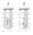
- FIG. 1is a schematic cross-sectional view of a portion of a bonded structure including a first element and a second element.
- FIG. 2is a schematic cross-sectional view of a portion of a bonded structure having a cavity.
- FIG. 3is a sectional plan view of the bonded structure of FIG. 2 .
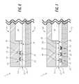
- FIG. 4is a schematic cross-sectional view of the bonded structure having a plurality of spaces for receiving getter material(s) disposed in the first and second elements.
- FIG. 5is a schematic cross-sectional view of a bonded structure having a first space comprising a first opening in the first element and a second space comprising a second opening in the second element, with the first and second spaces being laterally or horizontally spaced from one another.
- FIG. 6is a schematic cross-sectional view of a bonded structure in which a first space comprising a first opening in the second element and a second space comprising a second opening in the second element, with the first and second spaces being horizontally spaced.
- FIG. 7is a schematic cross-sectional view of a bonded structure in which an element has a plurality of spaces that are horizontally spaced from one another.
- FIG. 8is a sectional plan view of the bonded structure having a plurality of channels disposed around an interior region of the bonded structure.
- FIG. 9is a schematic side cross-sectional view of a bonded structure with a getter layer disposed in the cavity.
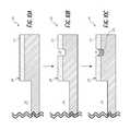
- FIG. 10Ais a cross sectional view of the first element prior to forming an opening for receiving a getter material.
- FIG. 10Bis a cross sectional view of the first element of FIG. 10A after forming the opening and prior to receiving the getter material.
- FIG. 10Cis a cross sectional view of the first element of FIG. 10B after disposing the getter material in the opening.
- FIG. 11Ais a cross sectional view of a bonded structure, according to an embodiment.
- FIG. 11Bis a cross sectional view of the bonded structure of FIG. 11A after forming an opening in the bonded structure.
- FIG. 11Cis a cross sectional view of the bonded structure of FIG. 11B after disposing a getter material in the opening.
- FIG. 11Dis a cross sectional view of the bonded structure of FIG. 11C after plugging the opening.
- FIG. 12is a schematic diagram of an electronic system incorporating one or more bonded structures.
- a bonded structurecan comprise a plurality of semiconductor elements bonded to one another along a bonding interface.
- An integrated devicecan be coupled to or formed with a semiconductor element.
- the bonded structurecan comprise a microelectromechanical systems (MEMS) device in which a cap (a first semiconductor element) is bonded to a carrier (a second semiconductor element).
- MEMS elementthe integrated device
- the element(s)can comprise other types of elements, such as optical elements, etc.
- the bonded structurecan comprise a getter material disposed between the first and second elements.
- the getter materialmay absorb and/or occlude incident moisture or gases.
- the getter materialcan prevent gases (or significantly reduce an amount of the gas(es)) from reaching interior regions and/or integrated devices of the bonded structure.
- the getter materialcan be disposed in a space provided along the bonding surface.
- the first and second elementscan be directly bonded without an intervening adhesive, e.g., such that bonding interfaces of the first and second elements contact one another.
- FIG. 1is a schematic cross sectional view of a portion of a bonded structure 1 according to various embodiments.
- the bonded structurecan include a first element 10 , a second element 12 , a getter material 24 disposed in a space or void 22 and an integrated device 15 .
- the integrated device 15can comprise any suitable type of device, such as an integrated circuit, a micro electro mechanical systems (MEMS) device, etc.
- MEMSmicro electro mechanical systems
- a first bonding surface 28 of the first element 10 and a second bonding surface 30 of the second element 12can be bonded at a bonding interface 32 by way of direct bonding, e.g., without an intervening adhesive.
- FIG. 2is a schematic side cross sectional view of a portion of the bonded structure 1 according to another embodiment.
- the bonded structure 1 of FIG. 2includes a cavity 26 for receiving an integrated device.
- the integrated device 15 shown in FIG. 1can be disposed in the cavity 26 in FIG. 2 .
- FIG. 3is a sectional plan view of the bonded structure 1 of FIG. 2 . It should be understood that the bonded structure 1 can include more than one integrated device 15 and/or more than one cavity 26 , in some embodiments.
- the second element 12can comprise a carrier to which the first element 10 is bonded.
- the carriercan comprise an integrated device die, such as a processor die configured to process signals transduced by the integrated device 15 .
- the integrated device 15can comprise a MEMS element, such as a MEMS switch, an accelerometer, a gyroscope, etc.
- the integrated device 15can be coupled to or formed with the first semiconductor element 10 or the second semiconductor element 12 .
- the carriercan comprise a substrate, such as a semiconductor substrate (e.g., a silicon interposer with conductive interconnects), a printed circuit board (PCB), a ceramic substrate, a glass substrate, or any other suitable carrier.
- a semiconductor substratee.g., a silicon interposer with conductive interconnects
- PCBprinted circuit board
- the carriercan transfer signals between the integrated device 15 and a larger packaging structure or electronic system (not shown).
- the carriercan comprise an integrated device die, such as a processor die configured to process signals transduced by the integrated device 15 .
- the integrated device 15can comprise a MEMS element, such as a MEMS switch, an accelerometer, a gyroscope, etc.
- the integrated device 15can be coupled to or formed with the first semiconductor element 10 or the second semiconductor element 12 .
- the integrated device die 15can be important to isolate or separate the integrated device die 15 from the outside environs, e.g., from exposure to gases and/or contaminants.
- gasessuch as hydrogen or oxygen gas
- leakage of any other gases from the outside environmente.g., oxygen, nitrogen, etc.
- the space 22can comprise a first opening 18 in the first element 10 and a second opening 20 in the second element 12 , such as in the embodiments of FIGS. 1 to 3 . Even though the first and second openings 18 , 20 shown in FIG. 1 may be generally aligned to define the space 22 , in practice, there can be offsets between positions of the first and second openings 18 , 20 . In some embodiments, the space 22 can be enclosed. However, as shown in some other embodiments, the space 22 may only comprise one opening in either the first or the second elements 10 , 12 (see FIGS. 6 and 7 ).
- the openings 18 , 20can comprise trenches formed at the bonding surface(s) 28 , 30 of the first and/or second elements 10 , 12 .
- the space or void 22 with the getter material 24can extend around the device in an effectively closed profile.
- the space or void 22can comprise a continuous channel around the integrated device 15 and/or the cavity 26 , as shown in FIG. 3 .
- the space 22may not comprise a continuous channel.
- the space 22can comprise a plurality of space portions and/or a plurality of channel portions around the integrated device 15 and/or the cavity 26 , which collectively define an effectively closed profile around the device 15 and/or cavity 26 .
- the space 22 with getter material 24can define an effectively closed profile around the device 15 and/or cavity 26 to seal the device 15 and/or cavity 26 from the outside environs, regardless of whether the space 20 is continuous or includes gaps.
- the disclosed embodimentscan utilize getter materials that can collect free gases incident to them by, for example, absorption and/or occlusion.
- getter materialscan have different properties.
- aluminum (Al)can have a getter capacity of about 1 Pa-l/mg against oxygen (O 2 ).
- Barium (Ba)can have a getter capacity of about 0.69 Pa-l/mg against carbon dioxide (CO 2 ), about 11.5 Pa-l/mg against hydrogen (H 2 ), and about 2 Pa-l/mg against (O 2 ).
- Titanium (Ti)can have about 4.4 Pa-l/mg against (O 2 ).
- the getter material 24can be selected based on the types of gases that are likely be present in the environment of which the bonded structure 1 would be used. Accordingly, the getter material 24 in the space 22 disposed along the bonding surface 32 can effectively provide seals for preserving hermetical or near-hermetical property for the integrated device 15 and/or the cavity 26 .
- the getter material 24can comprise one of or any two or more combination of Al, Ba, Ti, magnesium (Mg), niobium (Cb), zirconium (Zr), thorium (Th), phosphorus (P), vanadium (V), iron (Fe), and/or any other getter materials suitable.
- the getter material 24can fill the space 22 completely or partially.
- the getter material 24can be coated around an inner periphery of the space 22 .
- the getter material 24can comprise a powder form, solid form, liquid form, or any other suitable form for targeted purposes.
- the openings 18 , 20can receive two distinct types of getter material. Such embodiments can beneficially act on different gases at the bonding surface 32 .
- the same getter material 24can be provided in each element 10 , 12 . In other embodiments, each element 10 , 12 may utilize different getter materials.
- the first and second elementscan be bonded in any suitable manner, including by direct bonding.
- the direct bond between the first element 10 and the second element 12can include a direct bond between the first bonding surface 28 of the first element 10 and the second bonding surface 30 of the second element 12 .
- Preparation for bonding top surfaces of respective substrates 11 , 13can include provision of nonconductive layers 14 , 16 , such as silicon oxide, with exposed openings 18 , 20 .
- the bonding surfaces of the first element 10 and the second element 12can be polished to a very high degree of smoothness (e.g., less than 20 nm surface roughness, or more particularly, less than 5 nm surface roughness) for example, by chemical mechanical polishing (CMP).
- CMPchemical mechanical polishing
- the surfaces to be bondedmay be terminated with a suitable species and activated prior to bonding.
- the bonding surfaces 28 , 30 of the bonding layer to be bondedsuch as silicon oxide material
- the bonding surfaces 28 , 30 of the bonding layer to be bondedmay be very slightly etched for activation and exposed to a nitrogen-containing solution and terminated with a nitrogen-containing species.
- the surfaces 28 , 30 to be bondedmay be exposed to an ammonia dip after a very slight etch, and/or a nitrogen-containing plasma (with or without a separate etch).
- the interaction of the activated surfacescan cause the first bonding surface 28 of the first element 10 to directly bond with the second surface 30 of the second element 12 without an intervening adhesive, without application of external pressure, without application of voltage, and at room temperature.
- the bonding forces of the nonconductive regionscan include covalent bonds that are greater than Van der Waals bonds and exert significant forces between the conductive features.
- the bonding energy of the dielectric-dielectric surfacecan be in a range from 150-300 mJ/m 2 , which can increase to 1500-4000 mJ/m 2 after a period of heat treatment. Additional details of the direct bonding processes used in conjunction with each of the disclosed embodiments may be found throughout U.S. Pat. Nos.
- the elements 10 , 12can be bonded with an adhesive.
- the bonding surface 32can have a dimension d from an outer edge 17 to the integrated device 15 or the cavity 26 , for example, in a range of 10 ⁇ m to 600 ⁇ m, in a range of 10 ⁇ m to 80 ⁇ m, in a range of 40 ⁇ m to 60 ⁇ m, in a range of 100 ⁇ m to 600 ⁇ m, in a range of 200 ⁇ m to 300 ⁇ m, etc.
- FIGS. 4-9show alternative embodiments of the bonded structure 1 .
- FIG. 4is a schematic cross sectional view of the bonded structure 1 having the space 22 and a second space 23 disposed horizontally adjacent to each other for receiving the getter material 24 and a second getter material 25 , respectively.
- the components of FIG. 4may be the same as or generally similar to like-numbered components of FIGS. 1-3 .
- the space 22can comprise the first and second openings 18 , 20 formed in the respective first and second elements 10 , 12
- the second space 23can comprise third and fourth openings 19 , 21 formed in the respective first and second elements 10 , 12 .
- the space 22 and the nd space 23can comprise the same or different shapes and/or sizes.
- the openings 18 , 20 , 19 and 21can comprise the same or different shapes and/or sizes.
- the getter material 24 and the second getter material 25can comprise the same or different getter materials. It can be beneficial to have different getter materials 24 , 25 , in some embodiments. For example, different getter materials can act on different types gases to more effectively seal the integrated device and/or the cavity 26 within the bonded structure 1 .
- FIG. 5is a schematic cross sectional view of the bonded structure 1 having the space 22 comprising the first opening 18 in the first element 10 and the second space 23 comprising the second opening 20 in the second element 12 disposed horizontally adjacent to each other for receiving the getter material 24 and the second getter material 25 respectively.
- the components of FIG. 5may be the same as or generally similar to like-numbered components of FIGS. 1-4 .
- the first opening 18can be formed in the first element 10 and the second opening 20 can be formed in the second element 12 .
- the first opening 18 and the second opening 20can comprise the same or different shapes and/or sizes.
- first and second openings 18 , 20can be horizontally mismatched, for example, such that they do not together cooperate to define a common space to receive the getter material. Therefore, the first opening 18 and a portion of the second bonding surface 30 can define the space 22 , and the second opening 20 and a portion of the first bonding surface 28 can define the second space 23 .
- Such embodiments that physically separate the spaces 22 , 23can be beneficial because, different getter materials 24 , 25 may react with one another, which can affect the performance of the getter materials 24 , 25 when the spaces 22 , 23 are not separated from one another.
- getter filling processesmay limit the type of these reactive getter materials that are to be received within the elements (e.g., within the die or wafer (top or bottom)) e.g. screen printing methods.
- some filling processesmay be suitable for use with some devices or material sets (e.g., with one type of die, carrier, or substrate), and may be unsuitable for other types of devices.
- different processes and materialsmay be used to fill the spaces in the first and second elements 10 , 12 , respectively.
- FIG. 6is a schematic cross sectional view of the bonded structure 1 in which the space 22 comprises the opening 18 formed in the first element 10 and the second space 23 comprises the opening 19 formed in the first element 10 .
- the first and second spaces 22 , 23can be disposed horizontally adjacent to each other for receiving the getter material 24 and the second getter material 25 respectively.
- the components of FIG. 6may be the same as or generally similar to like-numbered components of FIGS. 1-5 .
- the opening 18 formed in the first element 10 and a first portion of the second bonding surface 30can comprise the first space 22
- the opening 19 formed in the first element 10 and a second portion of the second bonding surface 30can comprise the second space 23 .
- This embodimentcan be beneficial because the openings may be formed only on the first element such that formation of the openings can be simpler (e.g., fewer steps in a forming process, etc.) than forming openings in both the first and second elements 10 , 12 .
- having the openings 18 , 19 only in the first element 10can be beneficial since the first element can serve as a dummy element acting as a cap to form a cavity 26 .
- the second element 12can comprise a functional chip or device die; in such embodiments, providing the openings in only the first element 10 may obviate the use of openings in the second element 12 , e.g., an active chip or device die, which can beneficially avoid complications related to the wiring in second element 12 .
- openingscan be formed in the second element 12 as well.
- FIG. 7is a schematic cross sectional view of the bonded structure 1 in which the space 22 comprises the opening 20 formed in the second element 12 , the second space 23 comprises the opening 21 formed in the second element 12 , and the third space 40 comprises an opening 41 formed in the second element 12 .
- the openingscan be formed in the first element 10 , in some embodiments.
- the first, second and third spaces, 22 , 23 , 41can be disposed horizontally adjacent to each other for receiving the getter material 24 , the second getter material 25 and a third getter material 42 respectively.
- the components of FIG. 7may be the same as or generally similar to like-numbered components of FIGS. 1-6 .
- the third space 40can be provided for receiving the third getter material 42 .
- the opening 23 formed in the second element 12 and a third portion of the first bonding surface 28can form the third space 40 .
- increasing the number of spaces for receiving different getter materialscan be beneficial because, as explained above, different getter materials can act on different types of gases making the seal of the bonded structure 1 more hermetical.
- FIG. 8is a sectional plan view of the bonded structure 1 having the spaces 22 , 23 separated by gaps. Unless otherwise noted, the components of FIG. 8 may be the same as or generally similar to like-numbered components of FIGS. 1-7 . As illustrated in FIG. 8 , the spaces 22 , 23 are disposed to form channels comprising channel portions 52 , 53 . As shown, the channel portions 52 can be provided around the channel portions 53 . Although there are gaps between adjacent channel portions 52 , 53 , the illustrated embodiment can nevertheless provide an effectively closed profile for the cavity 26 . It should be understood that the channel portions 52 , 53 can have different shapes and/or sizes. In some embodiments, one of the spaces 22 , 23 can comprise a continuous channel and the other can comprise a discontinuous channel.
- different channel portions 52 , 53 of the spaces 22 , 23can comprise different getter materials suitable for an environment that the bonded structure 1 is to be used in. It should also be appreciated that any of the embodiments disclosed herein can utilize discontinuous channels to define the effectively closed profile.
- the bonded structure 1can have one or more electrical connections (e.g., wiring) between the channel portions 52 , 53 .
- the integrated device and/or the cavity 26can be accessed from outside of the bonded structure 1 through the connections.
- the channel portions 52can at least partially cover or overlap the gaps between the channel portions 53 that are disposed within the channel portions 52 .
- the channel portions 52may be positioned so as to block gases from passing through the gaps between the channel portions 53 .
- the channel portions 53may be positioned so as to block gases that pass through the gaps between the channel portions 52 from entering the cavity 26 .
- FIG. 9is a schematic cross sectional view of the bonded structure 1 with a getter layer 34 disposed in the cavity 26 .
- the components of FIG. 9may be the same as or generally similar to like-numbered components of FIGS. 1-8 .
- the embodiment illustrated in FIG. 9is similar to the embodiment illustrated in FIG. 2 except the bonded structure 1 of FIG. 9 further includes the getter layer 34 in the cavity 26 .
- the getter layer 34can be provided along an inner wall 35 of the cavity 26 .
- the getter layer 34can be activated when residual gas enters into the cavity 26 to absorb and/or occlude the residual gas to maintain ideal environment within the cavity 26 .
- the getter layer 34can be used to selectively alter the pressure within the cavity 26 .
- the bonded structurecan include more than one cavity 26 and each cavity may include different getter layer to alter the pressures in different cavities in the bonded structure 1 .
- the getter layer 34can comprise one of or any two or more combination of Al, Ba, Ti, Mg, Cb, Zr, Th, P, V, Fe, and/or any other getter materials suitable.
- FIGS. 10A-10Cshow steps for forming the first opening 18 in the first element 10 from the first bonding surface 28 and disposing the getter material 24 in the opening 18 .
- the first elementcan be provided.
- the cavity 26may be formed in the element 10 .
- the cavity 26can be formed in any suitable way, e.g., by etching, drilling, etc.
- the opening 18can be formed by way of, for example, etching (wet or dry), drilling (e.g., mechanical drilling, laser drilling, etc.), and/or any other suitable processes.
- the opening 18can be formed after forming the cavity 26 .
- the cavity 26can be formed before the opening 18 , or the cavity 26 and opening 18 can be formed at the same time.
- the getter material 24can be disposed in the opening 18 by way of, for example, electrochemical deposition, sputter coating, chemical vapor deposition (CVD), physical vapor deposition (PVD), screen printing, etc., and the process can vary depending on the particular material used as the getter material 24 .
- the getter material 24can be disposed in the opening completely or partially. It should be understood that a similar process can be applied to the second element 12 (see for example FIG. 2 ) to form openings in the second element 12 .
- a second elementcan be provided on the first bonding surface 28 to define the space 22 (see for example FIG. 2 ).
- FIGS. 11A-11Dshow steps for forming an trench 38 from a back surface 36 of the first element 10 , disposing the getter material 24 in the trench 38 , and forming the space or void 22 .
- a bonded structure 1can be provided in FIG. 11A .
- the trench 38can be formed by way of, for example, etching (wet, dry), drilling (e.g., mechanical drilling, laser drilling, etc.), and/or any other suitable processes. Referring to FIG.
- the getter material 24can be disposed in the trench 38 by way of, for example, electrochemical deposition, sputter coating, chemical vapor deposition (CVD), physical vapor deposition (PVD), screen printing, but the process can vary depending on the particular material used as the getter material 24 .
- a plug 56can be provided to plug the trench 38 to define the space 22 .
- the getter material 24can fully or partially fill the space 22 .
- the plugcan comprise, for example, a polymer material (e.g., epoxy, resin, epoxy mold compound, etc.). It should be understood that a similar process can be applied from a back surface 37 of the second element 12 .
- the bonded structure of FIG. 11Amay already include the space 22 along the bonding interface 32 after bonding the first and second elements 10 , 12 .
- the space 22may not have the getter material therein.
- the trench 38 from the back surface 36 of the first element 10can be provided only for disposing the getter material 24 into the space 22 already formed and not to form the openings for the space 22 .
- Thismay allow the trench 38 for providing the getter material 24 to have more flexible dimensional configurations than what is illustrated in FIGS. 11B-11D because the opening 38 may not depend on the dimensions of the space 22 in which the getter material 24 is disposed.
- the trench 38may be narrower than the space 22 .
- a thickness of the first element 10 from the front surface to the back surfaceis relatively thick (e.g., larger than 50 ⁇ m), because forming the trench 38 in such thick element may create a relatively big trench. If the space 22 were already formed, opening 38 from a back surface 36 may be narrower than a diameter of the space 22 , which reduces a dimension of the plug 56 .
- FIG. 12is a schematic diagram of an electronic system 80 incorporating one or more bonded structures 1 , according to various embodiments.
- the system 80can comprise any suitable type of electronic device, such as a mobile electronic device (e.g., a smartphone, a tablet computing device, a laptop computer, etc.), a desktop computer, an automobile or components thereof, a stereo system, a medical device, a camera, or any other suitable type of system.
- the electronic system 80can comprise a microprocessor, a graphics processor, an electronic recording device, or digital memory.
- the system 80can include one or more device packages 82 which are mechanically and electrically connected to the system 80 , e.g., by way of one or more motherboards. Each package 82 can comprise one or more bonded structures 1 .
- the system 80 shown in FIG. 8can comprise any of the bonded structures 1 and associated seals shown and described herein.
- a bonded structurein one aspect, can include a first element having a first bonding surface, a second element having a second bonding surface. The first and second bonding surfaces can be bonded to one another along a bonding interface.
- the bonded structurecan further include an integrated device that is coupled to or formed with the first element or the second element.
- the bonded structurecan also include a channel that is disposed along the bonding interface around the integrated device.
- the bonded structurecan also include a getter material disposed in the channel.
- the getter materialcan be configured to reduce the diffusion of gas into an interior region of the bonded structure.
- the first and second bonding surfacescan be directly bonded without an intervening adhesive.
- the bonding surfacecan have a dimension from an outer edge to the integrated device in a range of 10 ⁇ m to 600 ⁇ m.
- the channelcan include a first trench disposed through the first bonding surface and a second trench disposed through the second bonding surface.
- the bonded structurecan include a cavity and the integrated device can be disposed in the cavity.
- the channel and the getter materialcan be disposed around the cavity.
- the channelcan comprise a continuous channel surrounding the integrated device.
- a first group of the channel portionscan be filled with the getter material and a second group of the channel portions can be filled with a second getter material.
- the getter materialcan comprise at least one of titanium (Ti), tantalum (Ta), aluminum (Al), magnesium (Mg), thorium (Th), niobium (Cb), zirconium (Zr), and phosphorus (P).
- the channelcan be formed in only one of the first and second elements.
- the channelcan comprise a first trench disposed through the first bonding surface and a second trench disposed through the second bonding surface.
- the channelcan comprise a plurality of trenches that are offset laterally along the bonding interface.
- a bonded structurein another aspect, can include a first element, a second element that is directly bonded to the first element along a bonding interface without an intervening adhesive, and a getter material that is disposed in a space along the bonding surface.
- the getter materialis configured to reduce the diffusion of gas into an interior region of the bonded structure.
- the spacecan comprise a channel. In some embodiments, the space is enclosed.
- the bonded structurecan also include an integrated device that is coupled to or formed with the first element or the second element.
- the channelcan be disposed around the integrated device to define an effectively closed profile.
- a method of forming a bonded structurecan include providing a first element that has a first bonding surface. An opening is disposed through a portion of the first bonding surface. The method also includes disposing a getter material in the opening. The method further includes bonding a second bonding surface of a second element to the first bonding surface of the first element. The first and second bonding surfaces are bonded such that the opening and a portion of the second element cooperate to define a space configured to receive the getter material.
- the openingcan comprise a trench and the space can comprise a channel.
- the openingcan be provided by etching the first element from the first bonding surface to form a plurality of opening portions around the integrated device.
- the methodcan also include forming the opening and forming a second opening in the first element.
- the second openingare laterally offset from the opening. After the bonding, the second opening and a second portion of the second element can cooperate to define a second space configured to receive a second getter material.
- the methodcan also include forming the opening in the first element and forming a second opening in the second element through a portion of the second bonding surface.
- the opening and the second openingcan cooperate to define the space.
- the methodcan also include forming the opening by removing a portion of the first element from a back surface of the first element opposite the first bonding surface.
- the methodcan also include filling at least a portion of the opening from the back surface after disposing the getter material to form the for the getter material.
- the methodcan also include defining a cavity between the first element and the second element.
- the integrated devicecan be disposed in the cavity.
Landscapes
- Engineering & Computer Science (AREA)
- Microelectronics & Electronic Packaging (AREA)
- Computer Hardware Design (AREA)
- Power Engineering (AREA)
- Physics & Mathematics (AREA)
- Condensed Matter Physics & Semiconductors (AREA)
- General Physics & Mathematics (AREA)
- Manufacturing & Machinery (AREA)
- Micromachines (AREA)
Abstract
Description
- This application claims the benefit of U.S. Provisional Application No. 62/609,683 entitled “BONDED STRUCTURES,” filed Dec. 22, 2017, the entire disclosure of which is incorporated herein by reference for all purposes.
- The field generally relates to bonded structures, and in particular, to bonded structures having a getter material for sealing an internal portion of the bonded structures.
- In semiconductor device fabrication and packaging, some integrated devices are sealed from the outside environs in order to, e.g., reduce contamination or prevent damage to the integrated device. For example, some microelectromechanical systems (MEMS) devices include a cavity defined by a cap attached to a substrate with an adhesive such as solder. However, some adhesives may be permeable to gases, such that the gases can, over time, pass through the adhesive and into the cavity. Moisture or some gases, such as hydrogen or oxygen gas, can damage sensitive integrated devices. Other adhesives, such as solder, may have other long-term reliability issues. Accordingly, there remains a continued need for improved seals for integrated devices.
- Specific implementations of the invention will now be described with reference to the following drawings, which are provided by way of example, and not limitation.
FIG. 1 is a schematic cross-sectional view of a portion of a bonded structure including a first element and a second element.FIG. 2 is a schematic cross-sectional view of a portion of a bonded structure having a cavity.FIG. 3 is a sectional plan view of the bonded structure ofFIG. 2 .FIG. 4 is a schematic cross-sectional view of the bonded structure having a plurality of spaces for receiving getter material(s) disposed in the first and second elements.FIG. 5 is a schematic cross-sectional view of a bonded structure having a first space comprising a first opening in the first element and a second space comprising a second opening in the second element, with the first and second spaces being laterally or horizontally spaced from one another.FIG. 6 is a schematic cross-sectional view of a bonded structure in which a first space comprising a first opening in the second element and a second space comprising a second opening in the second element, with the first and second spaces being horizontally spaced.FIG. 7 is a schematic cross-sectional view of a bonded structure in which an element has a plurality of spaces that are horizontally spaced from one another.FIG. 8 is a sectional plan view of the bonded structure having a plurality of channels disposed around an interior region of the bonded structure.FIG. 9 is a schematic side cross-sectional view of a bonded structure with a getter layer disposed in the cavity.FIG. 10A is a cross sectional view of the first element prior to forming an opening for receiving a getter material.FIG. 10B is a cross sectional view of the first element ofFIG. 10A after forming the opening and prior to receiving the getter material.FIG. 10C is a cross sectional view of the first element ofFIG. 10B after disposing the getter material in the opening.FIG. 11A is a cross sectional view of a bonded structure, according to an embodiment.FIG. 11B is a cross sectional view of the bonded structure ofFIG. 11A after forming an opening in the bonded structure.FIG. 11C is a cross sectional view of the bonded structure ofFIG. 11B after disposing a getter material in the opening.FIG. 11D is a cross sectional view of the bonded structure ofFIG. 11C after plugging the opening.FIG. 12 is a schematic diagram of an electronic system incorporating one or more bonded structures.- Various embodiments disclosed herein relate to bonded structures that connect two elements (which may comprise semiconductor elements) in a manner that effectively seals interior portions and/or integrated devices of the semiconductor elements from the outside environs. For example, in some embodiments, a bonded structure can comprise a plurality of semiconductor elements bonded to one another along a bonding interface. An integrated device can be coupled to or formed with a semiconductor element. For example, in some embodiments, the bonded structure can comprise a microelectromechanical systems (MEMS) device in which a cap (a first semiconductor element) is bonded to a carrier (a second semiconductor element). A MEMS element (the integrated device) can be disposed in a cavity defined at least in part by the cap and the carrier. In other embodiments, the element(s) can comprise other types of elements, such as optical elements, etc.
- In some arrangements, the bonded structure can comprise a getter material disposed between the first and second elements. In some embodiments, the getter material may absorb and/or occlude incident moisture or gases. In some embodiments, the getter material can prevent gases (or significantly reduce an amount of the gas(es)) from reaching interior regions and/or integrated devices of the bonded structure. In some embodiments, the getter material can be disposed in a space provided along the bonding surface. In some embodiments, the first and second elements can be directly bonded without an intervening adhesive, e.g., such that bonding interfaces of the first and second elements contact one another.
FIG. 1 is a schematic cross sectional view of a portion of abonded structure 1 according to various embodiments. The bonded structure can include afirst element 10, asecond element 12, agetter material 24 disposed in a space orvoid 22 and an integrateddevice 15. The integrateddevice 15 can comprise any suitable type of device, such as an integrated circuit, a micro electro mechanical systems (MEMS) device, etc. In some embodiments, afirst bonding surface 28 of thefirst element 10 and asecond bonding surface 30 of thesecond element 12 can be bonded at abonding interface 32 by way of direct bonding, e.g., without an intervening adhesive.FIG. 2 is a schematic side cross sectional view of a portion of thebonded structure 1 according to another embodiment. Unlike thebonded structure 1 ofFIG. 1 , thebonded structure 1 ofFIG. 2 includes acavity 26 for receiving an integrated device. For example, the integrateddevice 15 shown inFIG. 1 can be disposed in thecavity 26 inFIG. 2 .FIG. 3 is a sectional plan view of thebonded structure 1 ofFIG. 2 . It should be understood that thebonded structure 1 can include more than one integrateddevice 15 and/or more than onecavity 26, in some embodiments.- In some embodiments, the
second element 12 can comprise a carrier to which thefirst element 10 is bonded. In some embodiments, the carrier can comprise an integrated device die, such as a processor die configured to process signals transduced by the integrateddevice 15. In some embodiments, theintegrated device 15 can comprise a MEMS element, such as a MEMS switch, an accelerometer, a gyroscope, etc. Theintegrated device 15 can be coupled to or formed with thefirst semiconductor element 10 or thesecond semiconductor element 12. In some embodiments, the carrier can comprise a substrate, such as a semiconductor substrate (e.g., a silicon interposer with conductive interconnects), a printed circuit board (PCB), a ceramic substrate, a glass substrate, or any other suitable carrier. In such embodiments, the carrier can transfer signals between theintegrated device 15 and a larger packaging structure or electronic system (not shown). In some embodiments, the carrier can comprise an integrated device die, such as a processor die configured to process signals transduced by theintegrated device 15. In some embodiments, theintegrated device 15 can comprise a MEMS element, such as a MEMS switch, an accelerometer, a gyroscope, etc. Theintegrated device 15 can be coupled to or formed with thefirst semiconductor element 10 or thesecond semiconductor element 12. - In some configurations, it can be important to isolate or separate the integrated device die15 from the outside environs, e.g., from exposure to gases and/or contaminants. For example, for some integrated devices, exposure to moisture or gases (such as hydrogen or oxygen gas) can damage the
integrated device 15 or other components. In other examples, leakage of any other gases from the outside environment (e.g., oxygen, nitrogen, etc.) may not be desired, as it may change the pressure inside the cavity, effectively altering the device performance. Accordingly, it can be important to provide a seal that effectively or substantially seals (e.g., hermetically or near-hermetically seals) the integrated device15 (FIG. 1 ) and/or the cavity26 (FIG. 2 ) from gases. - In some embodiments, the
space 22 can comprise afirst opening 18 in thefirst element 10 and asecond opening 20 in thesecond element 12, such as in the embodiments ofFIGS. 1 to 3 . Even though the first andsecond openings FIG. 1 may be generally aligned to define thespace 22, in practice, there can be offsets between positions of the first andsecond openings space 22 can be enclosed. However, as shown in some other embodiments, thespace 22 may only comprise one opening in either the first or thesecond elements 10,12 (seeFIGS. 6 and 7 ). Theopenings second elements getter material 24 can extend around the device in an effectively closed profile. In some embodiments, the space or void22 can comprise a continuous channel around theintegrated device 15 and/or thecavity 26, as shown inFIG. 3 . However, in other embodiments, thespace 22 may not comprise a continuous channel. Rather, thespace 22 can comprise a plurality of space portions and/or a plurality of channel portions around theintegrated device 15 and/or thecavity 26, which collectively define an effectively closed profile around thedevice 15 and/orcavity 26. Thus, thespace 22 withgetter material 24 can define an effectively closed profile around thedevice 15 and/orcavity 26 to seal thedevice 15 and/orcavity 26 from the outside environs, regardless of whether thespace 20 is continuous or includes gaps. - The disclosed embodiments can utilize getter materials that can collect free gases incident to them by, for example, absorption and/or occlusion. Different getter materials can have different properties. For example, aluminum (Al) can have a getter capacity of about 1 Pa-l/mg against oxygen (O2). Barium (Ba) can have a getter capacity of about 0.69 Pa-l/mg against carbon dioxide (CO2), about 11.5 Pa-l/mg against hydrogen (H2), and about 2 Pa-l/mg against (O2). Titanium (Ti) can have about 4.4 Pa-l/mg against (O2). Thus, in some embodiments, the
getter material 24 can be selected based on the types of gases that are likely be present in the environment of which the bondedstructure 1 would be used. Accordingly, thegetter material 24 in thespace 22 disposed along thebonding surface 32 can effectively provide seals for preserving hermetical or near-hermetical property for theintegrated device 15 and/or thecavity 26. In some embodiments, for example, thegetter material 24 can comprise one of or any two or more combination of Al, Ba, Ti, magnesium (Mg), niobium (Cb), zirconium (Zr), thorium (Th), phosphorus (P), vanadium (V), iron (Fe), and/or any other getter materials suitable. Thegetter material 24 can fill thespace 22 completely or partially. In some embodiments, thegetter material 24 can be coated around an inner periphery of thespace 22. In some embodiments, thegetter material 24 can comprise a powder form, solid form, liquid form, or any other suitable form for targeted purposes. In some embodiments, theopenings bonding surface 32. In some embodiments, thesame getter material 24 can be provided in eachelement element - The first and second elements can be bonded in any suitable manner, including by direct bonding. In some embodiments, the direct bond between the
first element 10 and thesecond element 12 can include a direct bond between thefirst bonding surface 28 of thefirst element 10 and thesecond bonding surface 30 of thesecond element 12. Preparation for bonding top surfaces ofrespective substrates nonconductive layers openings first element 10 and thesecond element 12 can be polished to a very high degree of smoothness (e.g., less than 20 nm surface roughness, or more particularly, less than 5 nm surface roughness) for example, by chemical mechanical polishing (CMP). In some embodiments, the surfaces to be bonded may be terminated with a suitable species and activated prior to bonding. For example, in some embodiments, the bonding surfaces28,30 of the bonding layer to be bonded, such as silicon oxide material, may be very slightly etched for activation and exposed to a nitrogen-containing solution and terminated with a nitrogen-containing species. As one example, thesurfaces second elements first bonding surface 28 of thefirst element 10 to directly bond with thesecond surface 30 of thesecond element 12 without an intervening adhesive, without application of external pressure, without application of voltage, and at room temperature. In various embodiments, the bonding forces of the nonconductive regions can include covalent bonds that are greater than Van der Waals bonds and exert significant forces between the conductive features. Prior to any heat treatment, the bonding energy of the dielectric-dielectric surface can be in a range from 150-300 mJ/m2, which can increase to 1500-4000 mJ/m2after a period of heat treatment. Additional details of the direct bonding processes used in conjunction with each of the disclosed embodiments may be found throughout U.S. Pat. Nos. 7,126,212; 8,153,505; 7,622,324; 7,602,070; 8,163,373; 8,389,378; and 8,735,219, and throughout U.S. Patent Application Publication Nos. 2017/0062366; 2016/0314346; 2017/0200711, the contents of each of which are hereby incorporated by reference herein in their entirety and for all purposes. In still other embodiments, theelements - In some embodiments, the
bonding surface 32 can have a dimension d from anouter edge 17 to theintegrated device 15 or thecavity 26, for example, in a range of 10 μm to 600 μm, in a range of 10 μm to 80 μm, in a range of 40 μm to 60 μm, in a range of 100 μm to 600 μm, in a range of 200 μm to 300 μm, etc. FIGS. 4-9 show alternative embodiments of the bondedstructure 1.FIG. 4 is a schematic cross sectional view of the bondedstructure 1 having thespace 22 and asecond space 23 disposed horizontally adjacent to each other for receiving thegetter material 24 and asecond getter material 25, respectively. Unless otherwise noted, the components ofFIG. 4 may be the same as or generally similar to like-numbered components ofFIGS. 1-3 . Thespace 22 can comprise the first andsecond openings second elements second space 23 can comprise third andfourth openings second elements space 22 and thend space 23 can comprise the same or different shapes and/or sizes. In other embodiments, theopenings getter material 24 and thesecond getter material 25 can comprise the same or different getter materials. It can be beneficial to havedifferent getter materials cavity 26 within the bondedstructure 1.FIG. 5 is a schematic cross sectional view of the bondedstructure 1 having thespace 22 comprising thefirst opening 18 in thefirst element 10 and thesecond space 23 comprising thesecond opening 20 in thesecond element 12 disposed horizontally adjacent to each other for receiving thegetter material 24 and thesecond getter material 25 respectively. Unless otherwise noted, the components ofFIG. 5 may be the same as or generally similar to like-numbered components ofFIGS. 1-4 . Unlike the bondedstructure 1 ofFIGS. 1-4 , thefirst opening 18 can be formed in thefirst element 10 and thesecond opening 20 can be formed in thesecond element 12. In some embodiments, thefirst opening 18 and thesecond opening 20 can comprise the same or different shapes and/or sizes. Further, as shown, the first andsecond openings first opening 18 and a portion of thesecond bonding surface 30 can define thespace 22, and thesecond opening 20 and a portion of thefirst bonding surface 28 can define thesecond space 23. Such embodiments that physically separate thespaces different getter materials getter materials spaces spaces FIG. 5 , different processes and materials may be used to fill the spaces in the first andsecond elements FIG. 6 is a schematic cross sectional view of the bondedstructure 1 in which thespace 22 comprises theopening 18 formed in thefirst element 10 and thesecond space 23 comprises theopening 19 formed in thefirst element 10. As shown, the first andsecond spaces getter material 24 and thesecond getter material 25 respectively. Unless otherwise noted, the components ofFIG. 6 may be the same as or generally similar to like-numbered components ofFIGS. 1-5 . InFIG. 6 , theopening 18 formed in thefirst element 10 and a first portion of thesecond bonding surface 30 can comprise thefirst space 22, and theopening 19 formed in thefirst element 10 and a second portion of thesecond bonding surface 30 can comprise thesecond space 23. This embodiment can be beneficial because the openings may be formed only on the first element such that formation of the openings can be simpler (e.g., fewer steps in a forming process, etc.) than forming openings in both the first andsecond elements openings first element 10 can be beneficial since the first element can serve as a dummy element acting as a cap to form acavity 26. Thesecond element 12 can comprise a functional chip or device die; in such embodiments, providing the openings in only thefirst element 10 may obviate the use of openings in thesecond element 12, e.g., an active chip or device die, which can beneficially avoid complications related to the wiring insecond element 12. However, it should be understood that, in some embodiments, openings can be formed in thesecond element 12 as well.FIG. 7 is a schematic cross sectional view of the bondedstructure 1 in which thespace 22 comprises theopening 20 formed in thesecond element 12, thesecond space 23 comprises theopening 21 formed in thesecond element 12, and thethird space 40 comprises anopening 41 formed in thesecond element 12. In should be understood that the openings can be formed in thefirst element 10, in some embodiments. As shown, the first, second and third spaces,22,23,41 can be disposed horizontally adjacent to each other for receiving thegetter material 24, thesecond getter material 25 and athird getter material 42 respectively. Unless otherwise noted, the components ofFIG. 7 may be the same as or generally similar to like-numbered components ofFIGS. 1-6 . The embodiment shown inFIGS. 6 and 7 are similar except in the embodiment inFIG. 7 thethird space 40 can be provided for receiving thethird getter material 42. Theopening 23 formed in thesecond element 12 and a third portion of thefirst bonding surface 28 can form thethird space 40. In some embodiments, increasing the number of spaces for receiving different getter materials can be beneficial because, as explained above, different getter materials can act on different types of gases making the seal of the bondedstructure 1 more hermetical.FIG. 8 is a sectional plan view of the bondedstructure 1 having thespaces FIG. 8 may be the same as or generally similar to like-numbered components ofFIGS. 1-7 . As illustrated inFIG. 8 , thespaces channel portions channel portions 52 can be provided around thechannel portions 53. Although there are gaps betweenadjacent channel portions cavity 26. It should be understood that thechannel portions spaces different channel portions spaces structure 1 is to be used in. It should also be appreciated that any of the embodiments disclosed herein can utilize discontinuous channels to define the effectively closed profile. In some embodiments, the bondedstructure 1 can have one or more electrical connections (e.g., wiring) between thechannel portions cavity 26 can be accessed from outside of the bondedstructure 1 through the connections. In the illustrated embodiment, thechannel portions 52 can at least partially cover or overlap the gaps between thechannel portions 53 that are disposed within thechannel portions 52. For example, thechannel portions 52 may be positioned so as to block gases from passing through the gaps between thechannel portions 53. Similarly, thechannel portions 53 may be positioned so as to block gases that pass through the gaps between thechannel portions 52 from entering thecavity 26.FIG. 9 is a schematic cross sectional view of the bondedstructure 1 with agetter layer 34 disposed in thecavity 26. Unless otherwise noted, the components ofFIG. 9 may be the same as or generally similar to like-numbered components ofFIGS. 1-8 . The embodiment illustrated inFIG. 9 is similar to the embodiment illustrated inFIG. 2 except the bondedstructure 1 ofFIG. 9 further includes thegetter layer 34 in thecavity 26. As shown, thegetter layer 34 can be provided along aninner wall 35 of thecavity 26. In some embodiments, thegetter layer 34 can be activated when residual gas enters into thecavity 26 to absorb and/or occlude the residual gas to maintain ideal environment within thecavity 26. In some embodiments, thegetter layer 34 can be used to selectively alter the pressure within thecavity 26. In some embodiments, the bonded structure can include more than onecavity 26 and each cavity may include different getter layer to alter the pressures in different cavities in the bondedstructure 1. As with the getter materials disposed between at the bonding surface, thegetter layer 34 can comprise one of or any two or more combination of Al, Ba, Ti, Mg, Cb, Zr, Th, P, V, Fe, and/or any other getter materials suitable.FIGS. 10A-10C show steps for forming thefirst opening 18 in thefirst element 10 from thefirst bonding surface 28 and disposing thegetter material 24 in theopening 18. InFIG. 10A , the first element can be provided. As shown inFIG. 10A , thecavity 26 may be formed in theelement 10. Thecavity 26 can be formed in any suitable way, e.g., by etching, drilling, etc. As shown inFIG. 10B theopening 18 can be formed by way of, for example, etching (wet or dry), drilling (e.g., mechanical drilling, laser drilling, etc.), and/or any other suitable processes. In the embodiment ofFIG. 10A , theopening 18 can be formed after forming thecavity 26. In other embodiments, however, thecavity 26 can be formed before theopening 18, or thecavity 26 andopening 18 can be formed at the same time. Referring toFIG. 10C , after theopening 18 is formed, thegetter material 24 can be disposed in theopening 18 by way of, for example, electrochemical deposition, sputter coating, chemical vapor deposition (CVD), physical vapor deposition (PVD), screen printing, etc., and the process can vary depending on the particular material used as thegetter material 24. Thegetter material 24 can be disposed in the opening completely or partially. It should be understood that a similar process can be applied to the second element12 (see for exampleFIG. 2 ) to form openings in thesecond element 12. In some embodiments, after thegetter material 24 is disposed in theopening 18, a second element can be provided on thefirst bonding surface 28 to define the space22 (see for exampleFIG. 2 ).FIGS. 11A-11D show steps for forming antrench 38 from aback surface 36 of thefirst element 10, disposing thegetter material 24 in thetrench 38, and forming the space or void22. InFIG. 11A , a bondedstructure 1 can be provided. As shown inFIG. 11B , thetrench 38 can be formed by way of, for example, etching (wet, dry), drilling (e.g., mechanical drilling, laser drilling, etc.), and/or any other suitable processes. Referring toFIG. 11C , after thetrench 38 is formed, thegetter material 24 can be disposed in thetrench 38 by way of, for example, electrochemical deposition, sputter coating, chemical vapor deposition (CVD), physical vapor deposition (PVD), screen printing, but the process can vary depending on the particular material used as thegetter material 24. Turning toFIG. 11D , aplug 56 can be provided to plug thetrench 38 to define thespace 22. Thegetter material 24 can fully or partially fill thespace 22. The plug can comprise, for example, a polymer material (e.g., epoxy, resin, epoxy mold compound, etc.). It should be understood that a similar process can be applied from aback surface 37 of thesecond element 12.- In some embodiments, the bonded structure of
FIG. 11A may already include thespace 22 along thebonding interface 32 after bonding the first andsecond elements space 22 may not have the getter material therein. In such embodiments, thetrench 38 from theback surface 36 of thefirst element 10 can be provided only for disposing thegetter material 24 into thespace 22 already formed and not to form the openings for thespace 22. This may allow thetrench 38 for providing thegetter material 24 to have more flexible dimensional configurations than what is illustrated inFIGS. 11B-11D because theopening 38 may not depend on the dimensions of thespace 22 in which thegetter material 24 is disposed. For example, thetrench 38 may be narrower than thespace 22. This can be beneficial, for example, when a thickness of thefirst element 10 from the front surface to the back surface is relatively thick (e.g., larger than 50 μm), because forming thetrench 38 in such thick element may create a relatively big trench. If thespace 22 were already formed, opening38 from aback surface 36 may be narrower than a diameter of thespace 22, which reduces a dimension of theplug 56. FIG. 12 is a schematic diagram of anelectronic system 80 incorporating one or more bondedstructures 1, according to various embodiments. Thesystem 80 can comprise any suitable type of electronic device, such as a mobile electronic device (e.g., a smartphone, a tablet computing device, a laptop computer, etc.), a desktop computer, an automobile or components thereof, a stereo system, a medical device, a camera, or any other suitable type of system. In some embodiments, theelectronic system 80 can comprise a microprocessor, a graphics processor, an electronic recording device, or digital memory. Thesystem 80 can include one or more device packages82 which are mechanically and electrically connected to thesystem 80, e.g., by way of one or more motherboards. Eachpackage 82 can comprise one or more bondedstructures 1. Thesystem 80 shown inFIG. 8 can comprise any of the bondedstructures 1 and associated seals shown and described herein.- In one aspect, a bonded structure is disclosed. The bonded structure can include a first element having a first bonding surface, a second element having a second bonding surface. The first and second bonding surfaces can be bonded to one another along a bonding interface. The bonded structure can further include an integrated device that is coupled to or formed with the first element or the second element. The bonded structure can also include a channel that is disposed along the bonding interface around the integrated device.
- In some embodiments, the bonded structure can also include a getter material disposed in the channel. The getter material can be configured to reduce the diffusion of gas into an interior region of the bonded structure. The first and second bonding surfaces can be directly bonded without an intervening adhesive. In some embodiments, the bonding surface can have a dimension from an outer edge to the integrated device in a range of 10 μm to 600 μm. The channel can include a first trench disposed through the first bonding surface and a second trench disposed through the second bonding surface.
- In some embodiments, the bonded structure can include a cavity and the integrated device can be disposed in the cavity. The channel and the getter material can be disposed around the cavity.
- In some embodiments, the channel can comprise a continuous channel surrounding the integrated device. A first group of the channel portions can be filled with the getter material and a second group of the channel portions can be filled with a second getter material.
- In some embodiments, the getter material can comprise at least one of titanium (Ti), tantalum (Ta), aluminum (Al), magnesium (Mg), thorium (Th), niobium (Cb), zirconium (Zr), and phosphorus (P).
- In some embodiments, the channel can be formed in only one of the first and second elements.
- In some embodiments, the channel can comprise a first trench disposed through the first bonding surface and a second trench disposed through the second bonding surface. The channel can comprise a plurality of trenches that are offset laterally along the bonding interface.
- In another aspect, a bonded structure is disclosed. The bonded structure can include a first element, a second element that is directly bonded to the first element along a bonding interface without an intervening adhesive, and a getter material that is disposed in a space along the bonding surface. The getter material is configured to reduce the diffusion of gas into an interior region of the bonded structure.
- In some embodiments, the space can comprise a channel. In some embodiments, the space is enclosed. The bonded structure can also include an integrated device that is coupled to or formed with the first element or the second element. The channel can be disposed around the integrated device to define an effectively closed profile.
- In another aspect a method of forming a bonded structure is disclosed. The method can include providing a first element that has a first bonding surface. An opening is disposed through a portion of the first bonding surface. The method also includes disposing a getter material in the opening. The method further includes bonding a second bonding surface of a second element to the first bonding surface of the first element. The first and second bonding surfaces are bonded such that the opening and a portion of the second element cooperate to define a space configured to receive the getter material.
- In some embodiments, the opening can comprise a trench and the space can comprise a channel. In some embodiments, the opening can be provided by etching the first element from the first bonding surface to form a plurality of opening portions around the integrated device.
- In some embodiments, the method can also include forming the opening and forming a second opening in the first element. The second opening are laterally offset from the opening. After the bonding, the second opening and a second portion of the second element can cooperate to define a second space configured to receive a second getter material.
- In some embodiments, the method can also include forming the opening in the first element and forming a second opening in the second element through a portion of the second bonding surface. The opening and the second opening can cooperate to define the space.
- In some embodiments, the method can also include forming the opening by removing a portion of the first element from a back surface of the first element opposite the first bonding surface. The method can also include filling at least a portion of the opening from the back surface after disposing the getter material to form the for the getter material.
- In some embodiments, the method can also include defining a cavity between the first element and the second element. The integrated device can be disposed in the cavity.
- For purposes of summarizing the disclosed embodiments and the advantages achieved over the prior art, certain objects and advantages have been described herein. Of course, it is to be understood that not necessarily all such objects or advantages may be achieved in accordance with any particular embodiment. Thus, for example, those skilled in the art will recognize that the disclosed implementations may be embodied or carried out in a manner that achieves or optimizes one advantage or group of advantages as taught or suggested herein without necessarily achieving other objects or advantages as may be taught or suggested herein.
- All of these embodiments are intended to be within the scope of this disclosure. These and other embodiments will become readily apparent to those skilled in the art from the following detailed description of the embodiments having reference to the attached figures, the claims not being limited to any particular embodiment(s) disclosed. Although this certain embodiments and examples have been disclosed herein, it will be understood by those skilled in the art that the disclosed implementations extend beyond the specifically disclosed embodiments to other alternative embodiments and/or uses and obvious modifications and equivalents thereof. In addition, while several variations have been shown and described in detail, other modifications will be readily apparent to those of skill in the art based upon this disclosure. It is also contemplated that various combinations or sub-combinations of the specific features and aspects of the embodiments may be made and still fall within the scope. It should be understood that various features and aspects of the disclosed embodiments can be combined with, or substituted for, one another in order to form varying modes of the disclosed implementations. Thus, it is intended that the scope of the subject matter herein disclosed should not be limited by the particular disclosed embodiments described above, but should be determined only by a fair reading of the claims that follow.
Claims (30)
Priority Applications (5)
| Application Number | Priority Date | Filing Date | Title |
|---|---|---|---|
| US16/011,525US11380597B2 (en) | 2017-12-22 | 2018-06-18 | Bonded structures |
| PCT/US2018/060044WO2019125639A1 (en) | 2017-12-22 | 2018-11-09 | Bonded structures |
| US17/829,185US11948847B2 (en) | 2017-12-22 | 2022-05-31 | Bonded structures |
| US18/545,136US20240120245A1 (en) | 2017-12-22 | 2023-12-19 | Bonded structures |
| US18/545,120US20240162102A1 (en) | 2017-12-22 | 2023-12-19 | Bonded structures |
Applications Claiming Priority (2)
| Application Number | Priority Date | Filing Date | Title |
|---|---|---|---|
| US201762609683P | 2017-12-22 | 2017-12-22 | |
| US16/011,525US11380597B2 (en) | 2017-12-22 | 2018-06-18 | Bonded structures |
Related Child Applications (1)
| Application Number | Title | Priority Date | Filing Date |
|---|---|---|---|
| US17/829,185ContinuationUS11948847B2 (en) | 2017-12-22 | 2022-05-31 | Bonded structures |
Publications (2)
| Publication Number | Publication Date |
|---|---|
| US20190198409A1true US20190198409A1 (en) | 2019-06-27 |
| US11380597B2 US11380597B2 (en) | 2022-07-05 |
Family
ID=66950600
Family Applications (4)
| Application Number | Title | Priority Date | Filing Date |
|---|---|---|---|
| US16/011,525ActiveUS11380597B2 (en) | 2017-12-22 | 2018-06-18 | Bonded structures |
| US17/829,185Active2038-07-17US11948847B2 (en) | 2017-12-22 | 2022-05-31 | Bonded structures |
| US18/545,120PendingUS20240162102A1 (en) | 2017-12-22 | 2023-12-19 | Bonded structures |
| US18/545,136PendingUS20240120245A1 (en) | 2017-12-22 | 2023-12-19 | Bonded structures |
Family Applications After (3)
| Application Number | Title | Priority Date | Filing Date |
|---|---|---|---|
| US17/829,185Active2038-07-17US11948847B2 (en) | 2017-12-22 | 2022-05-31 | Bonded structures |
| US18/545,120PendingUS20240162102A1 (en) | 2017-12-22 | 2023-12-19 | Bonded structures |
| US18/545,136PendingUS20240120245A1 (en) | 2017-12-22 | 2023-12-19 | Bonded structures |
Country Status (2)
| Country | Link |
|---|---|
| US (4) | US11380597B2 (en) |
| WO (1) | WO2019125639A1 (en) |
Cited By (74)
| Publication number | Priority date | Publication date | Assignee | Title |
|---|---|---|---|---|
| US10546832B2 (en) | 2016-12-21 | 2020-01-28 | Invensas Bonding Technologies, Inc. | Bonded structures |
| US10607937B2 (en) | 2015-12-18 | 2020-03-31 | Invensas Bonding Technologies, Inc. | Increased contact alignment tolerance for direct bonding |
| US10777533B2 (en) | 2012-08-30 | 2020-09-15 | Invensas Bonding Technologies, Inc. | Heterogeneous device |
| US10784191B2 (en) | 2017-03-31 | 2020-09-22 | Invensas Bonding Technologies, Inc. | Interface structures and methods for forming same |
| US10840205B2 (en) | 2017-09-24 | 2020-11-17 | Invensas Bonding Technologies, Inc. | Chemical mechanical polishing for hybrid bonding |
| US10879210B2 (en) | 2017-02-09 | 2020-12-29 | Invensas Bonding Technologies, Inc. | Bonded structures |
| US10879226B2 (en) | 2016-05-19 | 2020-12-29 | Invensas Bonding Technologies, Inc. | Stacked dies and methods for forming bonded structures |
| US10896902B2 (en) | 2016-01-13 | 2021-01-19 | Invensas Bonding Technologies, Inc. | Systems and methods for efficient transfer of semiconductor elements |
| US10923408B2 (en) | 2017-12-22 | 2021-02-16 | Invensas Bonding Technologies, Inc. | Cavity packages |
| US10998265B2 (en) | 2016-09-30 | 2021-05-04 | Invensas Bonding Technologies, Inc. | Interface structures and methods for forming same |
| US11004757B2 (en) | 2018-05-14 | 2021-05-11 | Invensas Bonding Technologies, Inc. | Bonded structures |
| US11011494B2 (en) | 2018-08-31 | 2021-05-18 | Invensas Bonding Technologies, Inc. | Layer structures for making direct metal-to-metal bonds at low temperatures in microelectronics |
| US11011418B2 (en) | 2005-08-11 | 2021-05-18 | Invensas Bonding Technologies, Inc. | 3D IC method and device |
| US11056390B2 (en) | 2015-06-24 | 2021-07-06 | Invensas Corporation | Structures and methods for reliable packages |
| US11158573B2 (en) | 2018-10-22 | 2021-10-26 | Invensas Bonding Technologies, Inc. | Interconnect structures |
| WO2021222020A1 (en)* | 2020-04-29 | 2021-11-04 | Elbit Systems Of America, Llc | Mems hermetic seal apparatus and methods |
| US11169326B2 (en) | 2018-02-26 | 2021-11-09 | Invensas Bonding Technologies, Inc. | Integrated optical waveguides, direct-bonded waveguide interface joints, optical routing and interconnects |
| US11195748B2 (en) | 2017-09-27 | 2021-12-07 | Invensas Corporation | Interconnect structures and methods for forming same |
| US11205600B2 (en) | 2014-03-12 | 2021-12-21 | Invensas Corporation | Integrated circuits protected by substrates with cavities, and methods of manufacture |
| US11205625B2 (en) | 2019-04-12 | 2021-12-21 | Invensas Bonding Technologies, Inc. | Wafer-level bonding of obstructive elements |
| US11244920B2 (en) | 2018-12-18 | 2022-02-08 | Invensas Bonding Technologies, Inc. | Method and structures for low temperature device bonding |
| US11257727B2 (en) | 2017-03-21 | 2022-02-22 | Invensas Bonding Technologies, Inc. | Seal for microelectronic assembly |
| US11264345B2 (en) | 2015-08-25 | 2022-03-01 | Invensas Bonding Technologies, Inc. | Conductive barrier direct hybrid bonding |
| US11373963B2 (en) | 2019-04-12 | 2022-06-28 | Invensas Bonding Technologies, Inc. | Protective elements for bonded structures |
| US11385278B2 (en) | 2019-05-23 | 2022-07-12 | Invensas Bonding Technologies, Inc. | Security circuitry for bonded structures |
| US11387214B2 (en) | 2017-06-15 | 2022-07-12 | Invensas Llc | Multi-chip modules formed using wafer-level processing of a reconstituted wafer |
| US11393779B2 (en) | 2018-06-13 | 2022-07-19 | Invensas Bonding Technologies, Inc. | Large metal pads over TSV |
| US20220246564A1 (en)* | 2018-08-29 | 2022-08-04 | Invensas Bonding Technologies, Inc. | Bond enhancement structure in microelectronics for trapping contaminants during direct-bonding processes |
| US11462419B2 (en) | 2018-07-06 | 2022-10-04 | Invensas Bonding Technologies, Inc. | Microelectronic assemblies |
| US11476213B2 (en) | 2019-01-14 | 2022-10-18 | Invensas Bonding Technologies, Inc. | Bonded structures without intervening adhesive |
| US11515291B2 (en) | 2018-08-28 | 2022-11-29 | Adeia Semiconductor Inc. | Integrated voltage regulator and passive components |
| US11515279B2 (en) | 2018-04-11 | 2022-11-29 | Adeia Semiconductor Bonding Technologies Inc. | Low temperature bonded structures |
| US11538781B2 (en) | 2020-06-30 | 2022-12-27 | Adeia Semiconductor Bonding Technologies Inc. | Integrated device packages including bonded structures |
| US11610846B2 (en) | 2019-04-12 | 2023-03-21 | Adeia Semiconductor Bonding Technologies Inc. | Protective elements for bonded structures including an obstructive element |
| US11626363B2 (en) | 2016-12-29 | 2023-04-11 | Adeia Semiconductor Bonding Technologies Inc. | Bonded structures with integrated passive component |
| US11652083B2 (en) | 2017-05-11 | 2023-05-16 | Adeia Semiconductor Bonding Technologies Inc. | Processed stacked dies |
| US11664357B2 (en) | 2018-07-03 | 2023-05-30 | Adeia Semiconductor Bonding Technologies Inc. | Techniques for joining dissimilar materials in microelectronics |
| US11710718B2 (en) | 2015-07-10 | 2023-07-25 | Adeia Semiconductor Technologies Llc | Structures and methods for low temperature bonding using nanoparticles |
| US11715730B2 (en) | 2017-03-16 | 2023-08-01 | Adeia Semiconductor Technologies Llc | Direct-bonded LED arrays including optical elements configured to transmit optical signals from LED elements |
| US11721653B2 (en) | 2019-12-23 | 2023-08-08 | Adeia Semiconductor Bonding Technologies Inc. | Circuitry for electrical redundancy in bonded structures |
| US11728313B2 (en) | 2018-06-13 | 2023-08-15 | Adeia Semiconductor Bonding Technologies Inc. | Offset pads over TSV |
| US11728273B2 (en) | 2020-09-04 | 2023-08-15 | Adeia Semiconductor Bonding Technologies Inc. | Bonded structure with interconnect structure |
| US11735523B2 (en) | 2020-05-19 | 2023-08-22 | Adeia Semiconductor Bonding Technologies Inc. | Laterally unconfined structure |
| US11742314B2 (en) | 2020-03-31 | 2023-08-29 | Adeia Semiconductor Bonding Technologies Inc. | Reliable hybrid bonded apparatus |
| US11742315B2 (en) | 2017-04-21 | 2023-08-29 | Adeia Semiconductor Bonding Technologies Inc. | Die processing |
| US11760059B2 (en) | 2003-05-19 | 2023-09-19 | Adeia Semiconductor Bonding Technologies Inc. | Method of room temperature covalent bonding |
| US11762200B2 (en) | 2019-12-17 | 2023-09-19 | Adeia Semiconductor Bonding Technologies Inc. | Bonded optical devices |
| US11764189B2 (en) | 2018-07-06 | 2023-09-19 | Adeia Semiconductor Bonding Technologies Inc. | Molded direct bonded and interconnected stack |
| US11764177B2 (en) | 2020-09-04 | 2023-09-19 | Adeia Semiconductor Bonding Technologies Inc. | Bonded structure with interconnect structure |
| US11791307B2 (en) | 2018-04-20 | 2023-10-17 | Adeia Semiconductor Bonding Technologies Inc. | DBI to SI bonding for simplified handle wafer |
| US11804377B2 (en) | 2018-04-05 | 2023-10-31 | Adeia Semiconductor Bonding Technologies, Inc. | Method for preparing a surface for direct-bonding |
| US11842894B2 (en) | 2019-12-23 | 2023-12-12 | Adeia Semiconductor Bonding Technologies Inc. | Electrical redundancy for bonded structures |
| US11855064B2 (en) | 2018-02-15 | 2023-12-26 | Adeia Semiconductor Bonding Technologies Inc. | Techniques for processing devices |
| US11894326B2 (en) | 2017-03-17 | 2024-02-06 | Adeia Semiconductor Bonding Technologies Inc. | Multi-metal contact structure |
| US11901281B2 (en) | 2019-03-11 | 2024-02-13 | Adeia Semiconductor Bonding Technologies Inc. | Bonded structures with integrated passive component |
| US11908739B2 (en) | 2017-06-05 | 2024-02-20 | Adeia Semiconductor Technologies Llc | Flat metal features for microelectronics applications |
| US11916054B2 (en) | 2018-05-15 | 2024-02-27 | Adeia Semiconductor Bonding Technologies Inc. | Stacked devices and methods of fabrication |
| US11929347B2 (en) | 2020-10-20 | 2024-03-12 | Adeia Semiconductor Technologies Llc | Mixed exposure for large die |
| US11935907B2 (en) | 2014-12-11 | 2024-03-19 | Adeia Semiconductor Technologies Llc | Image sensor device |
| US11955463B2 (en) | 2019-06-26 | 2024-04-09 | Adeia Semiconductor Bonding Technologies Inc. | Direct bonded stack structures for increased reliability and improved yield in microelectronics |
| US11973056B2 (en) | 2016-10-27 | 2024-04-30 | Adeia Semiconductor Technologies Llc | Methods for low temperature bonding using nanoparticles |
| US11978681B2 (en) | 2019-04-22 | 2024-05-07 | Adeia Semiconductor Bonding Technologies Inc. | Mitigating surface damage of probe pads in preparation for direct bonding of a substrate |
| US12009338B2 (en) | 2020-03-19 | 2024-06-11 | Adeia Semiconductor Bonding Technologies Inc. | Dimension compensation control for directly bonded structures |
| US12051621B2 (en) | 2016-12-28 | 2024-07-30 | Adeia Semiconductor Bonding Technologies Inc. | Microelectronic assembly from processed substrate |
| US12080672B2 (en) | 2019-09-26 | 2024-09-03 | Adeia Semiconductor Bonding Technologies Inc. | Direct gang bonding methods including directly bonding first element to second element to form bonded structure without adhesive |
| US12100676B2 (en) | 2018-04-11 | 2024-09-24 | Adeia Semiconductor Bonding Technologies Inc. | Low temperature bonded structures |
| US12211809B2 (en) | 2020-12-30 | 2025-01-28 | Adeia Semiconductor Bonding Technologies Inc. | Structure with conductive feature and method of forming same |
| US12270970B2 (en) | 2018-03-20 | 2025-04-08 | Adeia Semiconductor Bonding Technologies Inc. | Direct-bonded lamination for improved image clarity in optical devices |
| US12300634B2 (en) | 2021-08-02 | 2025-05-13 | Adeia Semiconductor Bonding Technologies Inc. | Protective semiconductor elements for bonded structures |
| US12341083B2 (en) | 2023-02-08 | 2025-06-24 | Adeia Semiconductor Bonding Technologies Inc. | Electronic device cooling structures bonded to semiconductor elements |
| US12374556B2 (en) | 2016-12-28 | 2025-07-29 | Adeia Semiconductor Bonding Technologies Inc. | Processing stacked substrates |
| US12374641B2 (en) | 2019-06-12 | 2025-07-29 | Adeia Semiconductor Bonding Technologies Inc. | Sealed bonded structures and methods for forming the same |
| US12406959B2 (en) | 2018-07-26 | 2025-09-02 | Adeia Semiconductor Bonding Technologies Inc. | Post CMP processing for hybrid bonding |
| US12424584B2 (en) | 2020-10-29 | 2025-09-23 | Adeia Semiconductor Bonding Technologies Inc. | Direct bonding methods and structures |
Families Citing this family (14)
| Publication number | Priority date | Publication date | Assignee | Title |
|---|---|---|---|---|
| US10672663B2 (en) | 2016-10-07 | 2020-06-02 | Xcelsis Corporation | 3D chip sharing power circuit |
| US10580735B2 (en) | 2016-10-07 | 2020-03-03 | Xcelsis Corporation | Stacked IC structure with system level wiring on multiple sides of the IC die |
| US11176450B2 (en) | 2017-08-03 | 2021-11-16 | Xcelsis Corporation | Three dimensional circuit implementing machine trained network |
| US11031285B2 (en) | 2017-10-06 | 2021-06-08 | Invensas Bonding Technologies, Inc. | Diffusion barrier collar for interconnects |
| US11380597B2 (en) | 2017-12-22 | 2022-07-05 | Invensas Bonding Technologies, Inc. | Bonded structures |
| US10991804B2 (en) | 2018-03-29 | 2021-04-27 | Xcelsis Corporation | Transistor level interconnection methodologies utilizing 3D interconnects |
| US10923413B2 (en) | 2018-05-30 | 2021-02-16 | Xcelsis Corporation | Hard IP blocks with physically bidirectional passageways |
| US10910344B2 (en) | 2018-06-22 | 2021-02-02 | Xcelsis Corporation | Systems and methods for releveled bump planes for chiplets |
| US11387202B2 (en) | 2019-03-01 | 2022-07-12 | Invensas Llc | Nanowire bonding interconnect for fine-pitch microelectronics |
| US10854578B2 (en) | 2019-03-29 | 2020-12-01 | Invensas Corporation | Diffused bitline replacement in stacked wafer memory |
| US12113054B2 (en) | 2019-10-21 | 2024-10-08 | Adeia Semiconductor Technologies Llc | Non-volatile dynamic random access memory |
| US11862602B2 (en) | 2019-11-07 | 2024-01-02 | Adeia Semiconductor Technologies Llc | Scalable architecture for reduced cycles across SOC |
| US11876076B2 (en) | 2019-12-20 | 2024-01-16 | Adeia Semiconductor Technologies Llc | Apparatus for non-volatile random access memory stacks |
| JP2024501017A (en) | 2020-12-28 | 2024-01-10 | アデイア セミコンダクター ボンディング テクノロジーズ インコーポレイテッド | Structure with through-substrate via and method for forming the same |
Citations (4)
| Publication number | Priority date | Publication date | Assignee | Title |
|---|---|---|---|---|
| WO2006100444A1 (en)* | 2005-03-22 | 2006-09-28 | Cambridge Display Technology Limited | Apparatus and method for increased device lifetime in an organic electro-luminescent device. |
| US7622324B2 (en)* | 2002-09-25 | 2009-11-24 | Ziptronix | Wafer bonding hermetic encapsulation |
| US20150068666A1 (en)* | 2012-05-18 | 2015-03-12 | Panasonic Intellectual Property Management Co., Ltd. | Production method of multiple panes |
| US20170137281A1 (en)* | 2014-07-18 | 2017-05-18 | Ulis | Method for Manufacturing a Device Comprising a Hermetically Sealed Vacuum Housing and Getter |
Family Cites Families (353)
| Publication number | Priority date | Publication date | Assignee | Title |
|---|---|---|---|---|
| JPH0272642A (en) | 1988-09-07 | 1990-03-12 | Nec Corp | Structure and method for connecting substrates |
| JPH0344067A (en) | 1989-07-11 | 1991-02-25 | Nec Corp | Laminating method of semiconductor substrate |
| CA2083072C (en) | 1991-11-21 | 1998-02-03 | Shinichi Hasegawa | Method for manufacturing polyimide multilayer wiring substrate |
| US6008126A (en) | 1992-04-08 | 1999-12-28 | Elm Technology Corporation | Membrane dielectric isolation IC fabrication |
| EP0651449B1 (en) | 1993-11-01 | 2002-02-13 | Matsushita Electric Industrial Co., Ltd. | Electronic component and method for producing the same |
| KR960009074A (en) | 1994-08-29 | 1996-03-22 | 모리시다 요이치 | Semiconductor device and manufacturing method thereof |
| DE4433330C2 (en) | 1994-09-19 | 1997-01-30 | Fraunhofer Ges Forschung | Method for producing semiconductor structures with advantageous high-frequency properties and a semiconductor wafer structure |
| JP3979687B2 (en) | 1995-10-26 | 2007-09-19 | アプライド マテリアルズ インコーポレイテッド | Method for improving film stability of halogen-doped silicon oxide films |
| JPH10112517A (en) | 1996-10-03 | 1998-04-28 | Ngk Spark Plug Co Ltd | Electronic components housing package |
| US6221753B1 (en) | 1997-01-24 | 2001-04-24 | Micron Technology, Inc. | Flip chip technique for chip assembly |
| JP4032454B2 (en) | 1997-06-27 | 2008-01-16 | ソニー株式会社 | Manufacturing method of three-dimensional circuit element |
| US6097096A (en) | 1997-07-11 | 2000-08-01 | Advanced Micro Devices | Metal attachment method and structure for attaching substrates at low temperatures |
| US6872984B1 (en) | 1998-07-29 | 2005-03-29 | Silicon Light Machines Corporation | Method of sealing a hermetic lid to a semiconductor die at an angle |
| JP2000100679A (en) | 1998-09-22 | 2000-04-07 | Canon Inc | Micro-region solid-state bonding method between substrates by thinning and device structure |
| JP3532788B2 (en) | 1999-04-13 | 2004-05-31 | 唯知 須賀 | Semiconductor device and manufacturing method thereof |
| JP2001102479A (en) | 1999-09-27 | 2001-04-13 | Toshiba Corp | Semiconductor integrated circuit device and method of manufacturing the same |
| US6984571B1 (en) | 1999-10-01 | 2006-01-10 | Ziptronix, Inc. | Three dimensional device integration method and integrated device |
| JP2001148436A (en) | 1999-11-22 | 2001-05-29 | Ngk Spark Plug Co Ltd | Ceramic package and its manufacturing method |
| US6902987B1 (en) | 2000-02-16 | 2005-06-07 | Ziptronix, Inc. | Method for low temperature bonding and bonded structure |
| JP4322402B2 (en) | 2000-06-22 | 2009-09-02 | 大日本印刷株式会社 | Printed wiring board and manufacturing method thereof |
| JP3440057B2 (en) | 2000-07-05 | 2003-08-25 | 唯知 須賀 | Semiconductor device and manufacturing method thereof |
| US6423640B1 (en) | 2000-08-09 | 2002-07-23 | Taiwan Semiconductor Manufacturing Co., Ltd. | Headless CMP process for oxide planarization |
| US6900549B2 (en) | 2001-01-17 | 2005-05-31 | Micron Technology, Inc. | Semiconductor assembly without adhesive fillets |
| JP2002353416A (en) | 2001-05-25 | 2002-12-06 | Sony Corp | Semiconductor storage device and method of manufacturing the same |
| US20020179921A1 (en) | 2001-06-02 | 2002-12-05 | Cohn Michael B. | Compliant hermetic package |
| US6818464B2 (en) | 2001-10-17 | 2004-11-16 | Hymite A/S | Double-sided etching technique for providing a semiconductor structure with through-holes, and a feed-through metalization process for sealing the through-holes |
| JP2003204074A (en) | 2001-10-29 | 2003-07-18 | Sharp Corp | Solar cell sealing film and method for manufacturing solar cell panel using the same |
| US20030113947A1 (en) | 2001-12-19 | 2003-06-19 | Vandentop Gilroy J. | Electrical/optical integration scheme using direct copper bonding |
| US6887769B2 (en) | 2002-02-06 | 2005-05-03 | Intel Corporation | Dielectric recess for wafer-to-wafer and die-to-die metal bonding and method of fabricating the same |
| US6762076B2 (en) | 2002-02-20 | 2004-07-13 | Intel Corporation | Process of vertically stacking multiple wafers supporting different active integrated circuit (IC) devices |
| US6876062B2 (en) | 2002-06-27 | 2005-04-05 | Taiwan Semiconductor Manufacturing Co., Ltd | Seal ring and die corner stress relief pattern design to protect against moisture and metallic impurities |
| US7105980B2 (en) | 2002-07-03 | 2006-09-12 | Sawtek, Inc. | Saw filter device and method employing normal temperature bonding for producing desirable filter production and performance characteristics |
| JP4083502B2 (en) | 2002-08-19 | 2008-04-30 | 株式会社フジミインコーポレーテッド | Polishing method and polishing composition used therefor |
| DE10238523B4 (en) | 2002-08-22 | 2014-10-02 | Epcos Ag | Encapsulated electronic component and method of manufacture |
| US7023093B2 (en) | 2002-10-24 | 2006-04-04 | International Business Machines Corporation | Very low effective dielectric constant interconnect Structures and methods for fabricating the same |
| US7354798B2 (en) | 2002-12-20 | 2008-04-08 | International Business Machines Corporation | Three-dimensional device fabrication method |
| JP4502173B2 (en) | 2003-02-03 | 2010-07-14 | ルネサスエレクトロニクス株式会社 | Semiconductor device and manufacturing method thereof |
| US6962835B2 (en) | 2003-02-07 | 2005-11-08 | Ziptronix, Inc. | Method for room temperature metal direct bonding |
| US6908027B2 (en) | 2003-03-31 | 2005-06-21 | Intel Corporation | Complete device layer transfer without edge exclusion via direct wafer bonding and constrained bond-strengthening process |
| US7109092B2 (en) | 2003-05-19 | 2006-09-19 | Ziptronix, Inc. | Method of room temperature covalent bonding |
| TWI275168B (en) | 2003-06-06 | 2007-03-01 | Sanyo Electric Co | Semiconductor device and method for making the same |
| US20040259325A1 (en) | 2003-06-19 | 2004-12-23 | Qing Gan | Wafer level chip scale hermetic package |
| WO2005031861A1 (en) | 2003-09-26 | 2005-04-07 | Tessera, Inc. | Structure and method of making capped chips including a flowable conductive medium |
| US6867073B1 (en) | 2003-10-21 | 2005-03-15 | Ziptronix, Inc. | Single mask via method and device |
| US7165896B2 (en) | 2004-02-12 | 2007-01-23 | Hymite A/S | Light transmitting modules with optical power monitoring |
| US7842948B2 (en) | 2004-02-27 | 2010-11-30 | Nvidia Corporation | Flip chip semiconductor die internal signal access system and method |
| US7952189B2 (en) | 2004-05-27 | 2011-05-31 | Chang-Feng Wan | Hermetic packaging and method of manufacture and use therefore |
| US7183622B2 (en) | 2004-06-30 | 2007-02-27 | Intel Corporation | Module integrating MEMS and passive components |
| US20060057945A1 (en) | 2004-09-16 | 2006-03-16 | Chia-Lin Hsu | Chemical mechanical polishing process |
| US20060076634A1 (en) | 2004-09-27 | 2006-04-13 | Lauren Palmateer | Method and system for packaging MEMS devices with incorporated getter |
| US8191756B2 (en) | 2004-11-04 | 2012-06-05 | Microchips, Inc. | Hermetically sealing using a cold welded tongue and groove structure |
| KR100498708B1 (en) | 2004-11-08 | 2005-07-01 | 옵토팩 주식회사 | Electronic package for semiconductor device and packaging method thereof |
| US7358106B2 (en) | 2005-03-03 | 2008-04-15 | Stellar Micro Devices | Hermetic MEMS package and method of manufacture |
| US7442570B2 (en) | 2005-03-18 | 2008-10-28 | Invensence Inc. | Method of fabrication of a AL/GE bonding in a wafer packaging environment and a product produced therefrom |
| JP2007019107A (en) | 2005-07-05 | 2007-01-25 | Shinko Electric Ind Co Ltd | Semiconductor device and its manufacturing method |
| US7485968B2 (en) | 2005-08-11 | 2009-02-03 | Ziptronix, Inc. | 3D IC method and device |
| US7582969B2 (en) | 2005-08-26 | 2009-09-01 | Innovative Micro Technology | Hermetic interconnect structure and method of manufacture |
| US20070045795A1 (en) | 2005-08-31 | 2007-03-01 | Mcbean Ronald V | MEMS package and method of forming the same |
| US8067769B2 (en) | 2005-11-25 | 2011-11-29 | Panasonic Electric Works Co., Ltd. | Wafer level package structure, and sensor device obtained from the same package structure |
| US7193423B1 (en) | 2005-12-12 | 2007-03-20 | International Business Machines Corporation | Wafer-to-wafer alignments |
| US7288458B2 (en) | 2005-12-14 | 2007-10-30 | Freescale Semiconductor, Inc. | SOI active layer with different surface orientation |
| US20070188054A1 (en) | 2006-02-13 | 2007-08-16 | Honeywell International Inc. | Surface acoustic wave packages and methods of forming same |
| US20080002460A1 (en) | 2006-03-01 | 2008-01-03 | Tessera, Inc. | Structure and method of making lidded chips |
| TWI299552B (en) | 2006-03-24 | 2008-08-01 | Advanced Semiconductor Eng | Package structure |
| US7972683B2 (en) | 2006-03-28 | 2011-07-05 | Innovative Micro Technology | Wafer bonding material with embedded conductive particles |
| DE102006016260B4 (en) | 2006-04-06 | 2024-07-18 | Fraunhofer-Gesellschaft zur Förderung der angewandten Forschung e.V. | Multiple component with several components containing active structures (MEMS) for later separation, flat substrate or flat cap structure, component with active structures that can be used in microsystem technology, single substrate or cap structure with active structures and method for producing a multiple component |
| US7462931B2 (en) | 2006-05-15 | 2008-12-09 | Innovative Micro Technology | Indented structure for encapsulated devices and method of manufacture |
| US7750488B2 (en) | 2006-07-10 | 2010-07-06 | Tezzaron Semiconductor, Inc. | Method for bonding wafers to produce stacked integrated circuits |
| US7430359B2 (en)* | 2006-10-02 | 2008-09-30 | Miradia, Inc. | Micromechanical system containing a microfluidic lubricant channel |
| US20080124835A1 (en) | 2006-11-03 | 2008-05-29 | International Business Machines Corporation | Hermetic seal and reliable bonding structures for 3d applications |
| JP4983219B2 (en) | 2006-11-22 | 2012-07-25 | 株式会社村田製作所 | Component built-in board |
| KR100833508B1 (en) | 2006-12-07 | 2008-05-29 | 한국전자통신연구원 | MEMs package and its method |
| US7803693B2 (en) | 2007-02-15 | 2010-09-28 | John Trezza | Bowed wafer hybridization compensation |
| JP4792143B2 (en) | 2007-02-22 | 2011-10-12 | 株式会社デンソー | Semiconductor device and manufacturing method thereof |
| US8513791B2 (en) | 2007-05-18 | 2013-08-20 | International Business Machines Corporation | Compact multi-port CAM cell implemented in 3D vertical integration |
| US7737513B2 (en) | 2007-05-30 | 2010-06-15 | Tessera, Inc. | Chip assembly including package element and integrated circuit chip |
| JP2009039843A (en) | 2007-08-10 | 2009-02-26 | Toshiba Corp | Electrical component and manufacturing method thereof |
| KR20090056044A (en) | 2007-11-29 | 2009-06-03 | 삼성전자주식회사 | Semiconductor device package and method of manufacturing same |
| JP2009238905A (en) | 2008-03-26 | 2009-10-15 | Nippon Telegr & Teleph Corp <Ntt> | Mounting structure and mounting method for semiconductor element |
| US8349635B1 (en) | 2008-05-20 | 2013-01-08 | Silicon Laboratories Inc. | Encapsulated MEMS device and method to form the same |
| US8513810B2 (en) | 2008-07-31 | 2013-08-20 | Nec Corporation | Semiconductor device and method of manufacturing same |
| US9893004B2 (en) | 2011-07-27 | 2018-02-13 | Broadpak Corporation | Semiconductor interposer integration |
| US8129828B2 (en) | 2008-09-29 | 2012-03-06 | Ngk Spark Plug Co., Ltd. | Wiring substrate with reinforcement |
| KR100945800B1 (en) | 2008-12-09 | 2010-03-05 | 김영혜 | Method for manufacturing heterogeneous bonded wafer |
| US8089144B2 (en) | 2008-12-17 | 2012-01-03 | Denso Corporation | Semiconductor device and method for manufacturing the same |
| US8058143B2 (en) | 2009-01-21 | 2011-11-15 | Freescale Semiconductor, Inc. | Substrate bonding with metal germanium silicon material |
| US8269671B2 (en) | 2009-01-27 | 2012-09-18 | International Business Machines Corporation | Simple radio frequency integrated circuit (RFIC) packages with integrated antennas |
| US8278749B2 (en) | 2009-01-30 | 2012-10-02 | Infineon Technologies Ag | Integrated antennas in wafer level package |
| US8476165B2 (en) | 2009-04-01 | 2013-07-02 | Tokyo Electron Limited | Method for thinning a bonding wafer |
| CN101554988B (en)* | 2009-04-30 | 2011-03-30 | 华中科技大学 | Wafer-level vacuum packaging method for micro-electromechanical systems |
| SE537499C2 (en) | 2009-04-30 | 2015-05-26 | Silex Microsystems Ab | Bonding material structure and process with bonding material structure |
| US20100288525A1 (en) | 2009-05-12 | 2010-11-18 | Alcatel-Lucent Usa, Incorporated | Electronic package and method of manufacture |
| EP2259018B1 (en) | 2009-05-29 | 2017-06-28 | Infineon Technologies AG | Gap control for die or layer bonding using intermediate layers of a micro-electromechanical system |
| FR2947481B1 (en) | 2009-07-03 | 2011-08-26 | Commissariat Energie Atomique | SIMPLIFIED COPPER-COPPER BONDING PROCESS |
| US8198174B2 (en) | 2009-08-05 | 2012-06-12 | International Business Machines Corporation | Air channel interconnects for 3-D integration |
| US8482132B2 (en) | 2009-10-08 | 2013-07-09 | International Business Machines Corporation | Pad bonding employing a self-aligned plated liner for adhesion enhancement |
| FR2953679B1 (en) | 2009-12-04 | 2012-06-01 | Thales Sa | HERMETIC ELECTRONIC HOUSING AND METHOD FOR HERMETICALLY ASSEMBLING A HOUSING |
| JP5115618B2 (en) | 2009-12-17 | 2013-01-09 | 株式会社デンソー | Semiconductor device |
| FR2954585B1 (en) | 2009-12-23 | 2012-03-02 | Soitec Silicon Insulator Technologies | METHOD FOR MAKING A HETEROSTRUCTURE WITH MINIMIZATION OF STRESS |
| JP5568786B2 (en) | 2009-12-24 | 2014-08-13 | 新光電気工業株式会社 | Semiconductor package manufacturing method and semiconductor package |
| US8455356B2 (en) | 2010-01-21 | 2013-06-04 | International Business Machines Corporation | Integrated void fill for through silicon via |
| GB2477492B (en) | 2010-01-27 | 2014-04-09 | Thales Holdings Uk Plc | Integrated circuit package |
| JP4900498B2 (en) | 2010-04-26 | 2012-03-21 | セイコーエプソン株式会社 | Electronic components |
| JP5517800B2 (en) | 2010-07-09 | 2014-06-11 | キヤノン株式会社 | Member for solid-state imaging device and method for manufacturing solid-state imaging device |
| TWI422080B (en) | 2010-08-20 | 2014-01-01 | Txc Corp | Enhanced gas - tightness of the oscillator device wafer - level package structure |
| US8330559B2 (en) | 2010-09-10 | 2012-12-11 | Taiwan Semiconductor Manufacturing Company, Ltd. | Wafer level packaging |
| US8411444B2 (en) | 2010-09-15 | 2013-04-02 | International Business Machines Corporation | Thermal interface material application for integrated circuit cooling |
| FR2966283B1 (en) | 2010-10-14 | 2012-11-30 | Soi Tec Silicon On Insulator Tech Sa | METHOD FOR PRODUCING A COLLAGE STRUCTURE |
| US8377798B2 (en) | 2010-11-10 | 2013-02-19 | Taiwan Semiconductor Manufacturing Co., Ltd | Method and structure for wafer to wafer bonding in semiconductor packaging |
| US9386688B2 (en) | 2010-11-12 | 2016-07-05 | Freescale Semiconductor, Inc. | Integrated antenna package |
| US8476146B2 (en) | 2010-12-03 | 2013-07-02 | Taiwan Semiconductor Manufacturing Company, Ltd. | Reducing wafer distortion through a low CTE layer |
| US8569090B2 (en) | 2010-12-03 | 2013-10-29 | Babak Taheri | Wafer level structures and methods for fabricating and packaging MEMS |
| US8620164B2 (en) | 2011-01-20 | 2013-12-31 | Intel Corporation | Hybrid III-V silicon laser formed by direct bonding |
| JP5696513B2 (en) | 2011-02-08 | 2015-04-08 | ソニー株式会社 | SOLID-STATE IMAGING DEVICE, ITS MANUFACTURING METHOD, AND ELECTRONIC DEVICE |
| US8988299B2 (en) | 2011-02-17 | 2015-03-24 | International Business Machines Corporation | Integrated antenna for RFIC package applications |
| US8847337B2 (en) | 2011-02-25 | 2014-09-30 | Evigia Systems, Inc. | Processes and mounting fixtures for fabricating electromechanical devices and devices formed therewith |
| US8395229B2 (en) | 2011-03-11 | 2013-03-12 | Institut National D'optique | MEMS-based getter microdevice |
| US8501537B2 (en) | 2011-03-31 | 2013-08-06 | Soitec | Methods for bonding semiconductor structures involving annealing processes, and bonded semiconductor structures formed using such methods |
| US8716105B2 (en) | 2011-03-31 | 2014-05-06 | Soitec | Methods for bonding semiconductor structures involving annealing processes, and bonded semiconductor structures and intermediate structures formed using such methods |
| TWI471951B (en) | 2011-03-31 | 2015-02-01 | Soitec Silicon On Insulator | Methods for bonding semiconductor structures involving annealing processes, and bonded semiconductor structures and intermediate structures formed using such methods |
| EP2514713B1 (en) | 2011-04-20 | 2013-10-02 | Tronics Microsystems S.A. | A micro-electromechanical system (MEMS) device |
| EP2717300B1 (en) | 2011-05-24 | 2020-03-18 | Sony Corporation | Semiconductor device |
| KR102282833B1 (en) | 2011-06-17 | 2021-07-27 | 가부시키가이샤 한도오따이 에네루기 켄큐쇼 | Transistor |
| US9540230B2 (en) | 2011-06-27 | 2017-01-10 | Invensense, Inc. | Methods for CMOS-MEMS integrated devices with multiple sealed cavities maintained at various pressures |
| JP5982748B2 (en) | 2011-08-01 | 2016-08-31 | ソニー株式会社 | SEMICONDUCTOR DEVICE, SEMICONDUCTOR DEVICE MANUFACTURING METHOD, AND ELECTRONIC DEVICE |
| US8697493B2 (en) | 2011-07-18 | 2014-04-15 | Soitec | Bonding surfaces for direct bonding of semiconductor structures |
| US8441131B2 (en) | 2011-09-12 | 2013-05-14 | Globalfoundries Inc. | Strain-compensating fill patterns for controlling semiconductor chip package interactions |
| TWI426572B (en) | 2011-10-20 | 2014-02-11 | Ind Tech Res Inst | Structure and process for microelectromechanical system-based sensor |
| EA038017B1 (en) | 2011-11-03 | 2021-06-23 | Фасткэп Системз Корпорейшн | Production logging instrument |
| US9139423B2 (en) | 2012-01-19 | 2015-09-22 | Taiwan Semiconductor Manufacturing Company, Ltd. | Micro electro mechanical system structures |
| CN103377911B (en) | 2012-04-16 | 2016-09-21 | 中国科学院微电子研究所 | Method for Improving Uniformity of Chemical Mechanical Planarization Process |
| US9139420B2 (en) | 2012-04-18 | 2015-09-22 | Taiwan Semiconductor Manufacturing Company, Ltd. | MEMS device structure and methods of forming same |
| JP2013243333A (en) | 2012-04-24 | 2013-12-05 | Tadatomo Suga | Chip-on wafer bonding method and bonding device and structure including chip and wafer |
| DE102012206732B4 (en) | 2012-04-24 | 2024-12-12 | Robert Bosch Gmbh | Method for producing a hybrid integrated component |
| KR102103811B1 (en) | 2012-04-24 | 2020-04-23 | 본드테크 가부시키가이샤 | Chip-on-wafer bonding method and bonding device, and structure comprising chip and wafer |
| FR2990314B1 (en) | 2012-05-03 | 2014-06-06 | Commissariat Energie Atomique | MICROELECTRONIC DEVICE FOR WIRELESS TRANSMISSION |
| US8809123B2 (en) | 2012-06-05 | 2014-08-19 | Taiwan Semiconductor Manufacturing Company, Ltd. | Three dimensional integrated circuit structures and hybrid bonding methods for semiconductor wafers |
| US9048283B2 (en) | 2012-06-05 | 2015-06-02 | Taiwan Semiconductor Manufacturing Company, Ltd. | Hybrid bonding systems and methods for semiconductor wafers |
| US9142517B2 (en) | 2012-06-05 | 2015-09-22 | Taiwan Semiconductor Manufacturing Company, Ltd. | Hybrid bonding mechanisms for semiconductor wafers |
| US8530997B1 (en) | 2012-07-31 | 2013-09-10 | Taiwan Semiconductor Manufacturing Company, Ltd. | Double seal ring |
| US9219144B2 (en)* | 2012-08-10 | 2015-12-22 | Infineon Technologies Austria Ag | Semiconductor device including a trench in a semiconductor substrate and method of manufacturing a semiconductor device |
| US8735219B2 (en) | 2012-08-30 | 2014-05-27 | Ziptronix, Inc. | Heterogeneous annealing method and device |
| CN103794538B (en) | 2012-10-31 | 2016-06-08 | 北京北方微电子基地设备工艺研究中心有限责任公司 | Electrostatic chuck and plasma processing device |
| US20140130595A1 (en) | 2012-11-12 | 2014-05-15 | Memsic, Inc. | Monolithic sensor package |
| US9511994B2 (en) | 2012-11-28 | 2016-12-06 | Invensense, Inc. | Aluminum nitride (AlN) devices with infrared absorption structural layer |
| DE102012224310A1 (en) | 2012-12-21 | 2014-06-26 | Tesa Se | Gettermaterial containing adhesive tape |
| US20140175655A1 (en) | 2012-12-22 | 2014-06-26 | Industrial Technology Research Institute | Chip bonding structure and manufacturing method thereof |
| US8916448B2 (en) | 2013-01-09 | 2014-12-23 | International Business Machines Corporation | Metal to metal bonding for stacked (3D) integrated circuits |
| US8766461B1 (en) | 2013-01-16 | 2014-07-01 | Texas Instruments Incorporated | Substrate with bond fingers |
| US8564076B1 (en) | 2013-01-30 | 2013-10-22 | Invensense, Inc. | Internal electrical contact for enclosed MEMS devices |
| US9452920B2 (en) | 2013-01-30 | 2016-09-27 | Invensense, Inc. | Microelectromechanical system device with internal direct electric coupling |
| US9136254B2 (en) | 2013-02-01 | 2015-09-15 | Invensas Corporation | Microelectronic package having wire bond vias and stiffening layer |
| US9287188B2 (en) | 2013-02-05 | 2016-03-15 | Taiwan Semiconductor Manufacturing Company, Ltd. | Method and apparatus for a seal ring structure |
| TWI518991B (en) | 2013-02-08 | 2016-01-21 | Sj Antenna Design | Integrated antenna and integrated circuit components of the shielding module |
| US20140225206A1 (en) | 2013-02-11 | 2014-08-14 | Yizhen Lin | Pressure level adjustment in a cavity of a semiconductor die |
| US8946784B2 (en) | 2013-02-18 | 2015-02-03 | Taiwan Semiconductor Manufacturing Company, Ltd. | Method and apparatus for image sensor packaging |
| US9469527B2 (en) | 2013-03-14 | 2016-10-18 | Taiwan Semiconductor Manufacturing Company, Ltd. | MEMS pressure sensor and microphone devices having through-vias and methods of forming same |
| US9443796B2 (en) | 2013-03-15 | 2016-09-13 | Taiwan Semiconductor Manufacturing Company, Ltd. | Air trench in packages incorporating hybrid bonding |
| US8802538B1 (en) | 2013-03-15 | 2014-08-12 | Taiwan Semiconductor Manufacturing Company, Ltd. | Methods for hybrid wafer bonding |
| US9119313B2 (en) | 2013-04-25 | 2015-08-25 | Intel Corporation | Package substrate with high density interconnect design to capture conductive features on embedded die |
| JP6020341B2 (en) | 2013-05-09 | 2016-11-02 | 株式会社デンソー | Capacitive physical quantity sensor and manufacturing method thereof |
| JPWO2014184988A1 (en) | 2013-05-16 | 2017-02-23 | パナソニックIpマネジメント株式会社 | Semiconductor device and manufacturing method thereof |
| US9064937B2 (en) | 2013-05-30 | 2015-06-23 | International Business Machines Corporation | Substrate bonding with diffusion barrier structures |
| US9136233B2 (en) | 2013-06-06 | 2015-09-15 | STMicroelctronis (Crolles 2) SAS | Process for fabricating a three-dimensional integrated structure with improved heat dissipation, and corresponding three-dimensional integrated structure |
| EP2813465B1 (en) | 2013-06-12 | 2020-01-15 | Tronic's Microsystems | MEMS device with getter layer |
| CN104249991B (en) | 2013-06-26 | 2016-08-10 | 中芯国际集成电路制造(上海)有限公司 | MEMS and preparation method thereof |
| US10273147B2 (en) | 2013-07-08 | 2019-04-30 | Motion Engine Inc. | MEMS components and method of wafer-level manufacturing thereof |
| US9929050B2 (en) | 2013-07-16 | 2018-03-27 | Taiwan Semiconductor Manufacturing Company, Ltd. | Mechanisms for forming three-dimensional integrated circuit (3DIC) stacking structure |
| US9723716B2 (en) | 2013-09-27 | 2017-08-01 | Infineon Technologies Ag | Contact pad structure, an electronic component, and a method for manufacturing a contact pad structure |
| KR20160036666A (en) | 2013-09-27 | 2016-04-04 | 인텔 코포레이션 | Die package with superposer substrate for passive components |
| US9035451B2 (en) | 2013-09-30 | 2015-05-19 | Taiwan Semiconductor Manufacturing Co., Ltd. | Wafer level sealing methods with different vacuum levels for MEMS sensors |
| US9617150B2 (en) | 2013-10-09 | 2017-04-11 | Taiwan Semiconductor Manufacturing Co., Ltd. | Micro-electro mechanical system (MEMS) device having a blocking layer formed between closed chamber and a dielectric layer of a CMOS substrate |
| US10464836B2 (en) | 2013-10-10 | 2019-11-05 | Medtronic, Inc. | Hermetic conductive feedthroughs for a semiconductor wafer |
| US9257399B2 (en) | 2013-10-17 | 2016-02-09 | Taiwan Semiconductor Manufacturing Company, Ltd. | 3D integrated circuit and methods of forming the same |
| KR20150058940A (en) | 2013-11-21 | 2015-05-29 | 삼성전자주식회사 | Semiconductor package having heat spreader |
| JP2015100886A (en) | 2013-11-26 | 2015-06-04 | セイコーエプソン株式会社 | Electronic devices and electronic equipment |
| JP2015115446A (en) | 2013-12-11 | 2015-06-22 | 株式会社東芝 | Manufacturing method of semiconductor device |
| US9437572B2 (en) | 2013-12-18 | 2016-09-06 | Taiwan Semiconductor Manufacturing Company, Ltd. | Conductive pad structure for hybrid bonding and methods of forming same |
| US9773742B2 (en) | 2013-12-18 | 2017-09-26 | Intel Corporation | Embedded millimeter-wave phased array module |
| JP2015153791A (en) | 2014-02-11 | 2015-08-24 | 三菱電機株式会社 | Method for manufacturing hermetic seal type semiconductor device, and hermetic seal type semiconductor device |
| US20150262902A1 (en) | 2014-03-12 | 2015-09-17 | Invensas Corporation | Integrated circuits protected by substrates with cavities, and methods of manufacture |
| US9299736B2 (en) | 2014-03-28 | 2016-03-29 | Taiwan Semiconductor Manufacturing Company, Ltd. | Hybrid bonding with uniform pattern density |
| US9230941B2 (en) | 2014-03-28 | 2016-01-05 | Taiwan Semiconductor Manufacturing Company, Ltd. | Bonding structure for stacked semiconductor devices |
| US9878901B2 (en) | 2014-04-04 | 2018-01-30 | Analog Devices, Inc. | Fabrication of tungsten MEMS structures |
| US9472458B2 (en) | 2014-06-04 | 2016-10-18 | Semiconductor Components Industries, Llc | Method of reducing residual contamination in singulated semiconductor die |
| KR102275705B1 (en) | 2014-07-11 | 2021-07-09 | 삼성전자주식회사 | Wafer-to-wafer bonding structure |
| US9620464B2 (en) | 2014-08-13 | 2017-04-11 | International Business Machines Corporation | Wireless communications package with integrated antennas and air cavity |
| US9536848B2 (en) | 2014-10-16 | 2017-01-03 | Globalfoundries Inc. | Bond pad structure for low temperature flip chip bonding |
| US9394161B2 (en) | 2014-11-14 | 2016-07-19 | Taiwan Semiconductor Manufacturing Co., Ltd. | MEMS and CMOS integration with low-temperature bonding |
| JP2016099224A (en) | 2014-11-21 | 2016-05-30 | セイコーエプソン株式会社 | Physical quantity sensor, electronic apparatus and moving body |
| US9899442B2 (en) | 2014-12-11 | 2018-02-20 | Invensas Corporation | Image sensor device |
| US9331043B1 (en) | 2015-01-30 | 2016-05-03 | Invensas Corporation | Localized sealing of interconnect structures in small gaps |
| JP5931246B1 (en) | 2015-04-03 | 2016-06-08 | 田中貴金属工業株式会社 | Package manufacturing method and package manufactured by the method |
| US9738516B2 (en) | 2015-04-29 | 2017-08-22 | Taiwan Semiconductor Manufacturing Co., Ltd. | Structure to reduce backside silicon damage |
| US9741620B2 (en) | 2015-06-24 | 2017-08-22 | Invensas Corporation | Structures and methods for reliable packages |
| US10315915B2 (en) | 2015-07-02 | 2019-06-11 | Kionix, Inc. | Electronic systems with through-substrate interconnects and MEMS device |
| US9656852B2 (en) | 2015-07-06 | 2017-05-23 | Taiwan Semiconductor Manufacturing Company Ltd. | CMOS-MEMS device structure, bonding mesa structure and associated method |
| US10886250B2 (en) | 2015-07-10 | 2021-01-05 | Invensas Corporation | Structures and methods for low temperature bonding using nanoparticles |
| US10075657B2 (en) | 2015-07-21 | 2018-09-11 | Fermi Research Alliance, Llc | Edgeless large area camera system |
| US9728521B2 (en) | 2015-07-23 | 2017-08-08 | Taiwan Semiconductor Manufacturing Co., Ltd. | Hybrid bond using a copper alloy for yield improvement |
| US9559081B1 (en) | 2015-08-21 | 2017-01-31 | Apple Inc. | Independent 3D stacking |
| US9953941B2 (en) | 2015-08-25 | 2018-04-24 | Invensas Bonding Technologies, Inc. | Conductive barrier direct hybrid bonding |
| US9650241B2 (en) | 2015-09-17 | 2017-05-16 | Invensense, Inc. | Method for providing a MEMS device with a plurality of sealed enclosures having uneven standoff structures and MEMS device thereof |
| WO2017100256A1 (en) | 2015-12-08 | 2017-06-15 | Skyworks Solutions, Inc. | Transient liquid phase material bonding and sealing structures and methods of forming same |
| US9496239B1 (en) | 2015-12-11 | 2016-11-15 | International Business Machines Corporation | Nitride-enriched oxide-to-oxide 3D wafer bonding |
| US9852988B2 (en) | 2015-12-18 | 2017-12-26 | Invensas Bonding Technologies, Inc. | Increased contact alignment tolerance for direct bonding |
| US9972603B2 (en) | 2015-12-29 | 2018-05-15 | Taiwan Semiconductor Manufacturing Co., Ltd. | Seal-ring structure for stacking integrated circuits |
| US9881882B2 (en) | 2016-01-06 | 2018-01-30 | Mediatek Inc. | Semiconductor package with three-dimensional antenna |
| US9923011B2 (en) | 2016-01-12 | 2018-03-20 | Taiwan Semiconductor Manufacturing Co., Ltd. | Semiconductor device structure with stacked semiconductor dies |
| US10446532B2 (en) | 2016-01-13 | 2019-10-15 | Invensas Bonding Technologies, Inc. | Systems and methods for efficient transfer of semiconductor elements |
| US10636767B2 (en) | 2016-02-29 | 2020-04-28 | Invensas Corporation | Correction die for wafer/die stack |
| US10026716B2 (en) | 2016-04-15 | 2018-07-17 | Taiwan Semiconductor Manufacturing Company, Ltd. | 3DIC formation with dies bonded to formed RDLs |
| US10273141B2 (en) | 2016-04-26 | 2019-04-30 | Taiwan Semiconductor Manufacturing Co., Ltd. | Rough layer for better anti-stiction deposition |
| US10204893B2 (en) | 2016-05-19 | 2019-02-12 | Invensas Bonding Technologies, Inc. | Stacked dies and methods for forming bonded structures |
| KR102505856B1 (en) | 2016-06-09 | 2023-03-03 | 삼성전자 주식회사 | wafer-to-wafer bonding structure |
| US9941241B2 (en) | 2016-06-30 | 2018-04-10 | International Business Machines Corporation | Method for wafer-wafer bonding |
| US9892961B1 (en) | 2016-08-09 | 2018-02-13 | International Business Machines Corporation | Air gap spacer formation for nano-scale semiconductor devices |
| US10062656B2 (en) | 2016-08-15 | 2018-08-28 | Taiwan Semiconductor Manufacturing Co., Ltd. | Composite bond structure in stacked semiconductor structure |
| US10446487B2 (en) | 2016-09-30 | 2019-10-15 | Invensas Bonding Technologies, Inc. | Interface structures and methods for forming same |
| US10672663B2 (en) | 2016-10-07 | 2020-06-02 | Xcelsis Corporation | 3D chip sharing power circuit |
| US10580735B2 (en) | 2016-10-07 | 2020-03-03 | Xcelsis Corporation | Stacked IC structure with system level wiring on multiple sides of the IC die |
| US11176450B2 (en) | 2017-08-03 | 2021-11-16 | Xcelsis Corporation | Three dimensional circuit implementing machine trained network |
| US9834435B1 (en) | 2016-11-29 | 2017-12-05 | Taiwan Semiconductor Manufacturing Co., Ltd. | Structure and formation method of semiconductor device structure |
| US10163750B2 (en) | 2016-12-05 | 2018-12-25 | Taiwan Semiconductor Manufacturing Company, Ltd. | Package structure for heat dissipation |
| US10453832B2 (en) | 2016-12-15 | 2019-10-22 | Taiwan Semiconductor Manufacturing Co., Ltd. | Seal ring structures and methods of forming same |
| US10002844B1 (en) | 2016-12-21 | 2018-06-19 | Invensas Bonding Technologies, Inc. | Bonded structures |
| CN117878055A (en) | 2016-12-28 | 2024-04-12 | 艾德亚半导体接合科技有限公司 | Stacking substrate processing |
| US20180182665A1 (en) | 2016-12-28 | 2018-06-28 | Invensas Bonding Technologies, Inc. | Processed Substrate |
| US20180190583A1 (en) | 2016-12-29 | 2018-07-05 | Invensas Bonding Technologies, Inc. | Bonded structures with integrated passive component |
| TWI837879B (en) | 2016-12-29 | 2024-04-01 | 美商艾德亞半導體接合科技有限公司 | Bonded structures with integrated passive component |
| US10276909B2 (en) | 2016-12-30 | 2019-04-30 | Invensas Bonding Technologies, Inc. | Structure comprising at least a first element bonded to a carrier having a closed metallic channel waveguide formed therein |
| US10431614B2 (en) | 2017-02-01 | 2019-10-01 | Semiconductor Components Industries, Llc | Edge seals for semiconductor packages |
| EP3580166A4 (en) | 2017-02-09 | 2020-09-02 | Invensas Bonding Technologies, Inc. | Bonded structures |
| WO2018169968A1 (en) | 2017-03-16 | 2018-09-20 | Invensas Corporation | Direct-bonded led arrays and applications |
| US10790240B2 (en) | 2017-03-17 | 2020-09-29 | Taiwan Semiconductor Manufacturing Co., Ltd. | Metal line design for hybrid-bonding application |
| US10515913B2 (en) | 2017-03-17 | 2019-12-24 | Invensas Bonding Technologies, Inc. | Multi-metal contact structure |
| US10508030B2 (en) | 2017-03-21 | 2019-12-17 | Invensas Bonding Technologies, Inc. | Seal for microelectronic assembly |
| JP6640780B2 (en) | 2017-03-22 | 2020-02-05 | キオクシア株式会社 | Semiconductor device manufacturing method and semiconductor device |
| US10784191B2 (en) | 2017-03-31 | 2020-09-22 | Invensas Bonding Technologies, Inc. | Interface structures and methods for forming same |
| US10269756B2 (en) | 2017-04-21 | 2019-04-23 | Invensas Bonding Technologies, Inc. | Die processing |
| US10580823B2 (en) | 2017-05-03 | 2020-03-03 | United Microelectronics Corp. | Wafer level packaging method |
| US10879212B2 (en) | 2017-05-11 | 2020-12-29 | Invensas Bonding Technologies, Inc. | Processed stacked dies |
| US10446441B2 (en) | 2017-06-05 | 2019-10-15 | Invensas Corporation | Flat metal features for microelectronics applications |
| US10217720B2 (en) | 2017-06-15 | 2019-02-26 | Invensas Corporation | Multi-chip modules formed using wafer-level processing of a reconstitute wafer |
| US10840205B2 (en) | 2017-09-24 | 2020-11-17 | Invensas Bonding Technologies, Inc. | Chemical mechanical polishing for hybrid bonding |
| US11195748B2 (en) | 2017-09-27 | 2021-12-07 | Invensas Corporation | Interconnect structures and methods for forming same |
| US11031285B2 (en) | 2017-10-06 | 2021-06-08 | Invensas Bonding Technologies, Inc. | Diffusion barrier collar for interconnects |
| US11251157B2 (en) | 2017-11-01 | 2022-02-15 | Taiwan Semiconductor Manufacturing Company, Ltd. | Die stack structure with hybrid bonding structure and method of fabricating the same and package |
| US10312201B1 (en) | 2017-11-30 | 2019-06-04 | Taiwan Semiconductor Manufacturing Company, Ltd. | Seal ring for hybrid-bond |
| US11011503B2 (en) | 2017-12-15 | 2021-05-18 | Invensas Bonding Technologies, Inc. | Direct-bonded optoelectronic interconnect for high-density integrated photonics |
| US10923408B2 (en) | 2017-12-22 | 2021-02-16 | Invensas Bonding Technologies, Inc. | Cavity packages |
| US11380597B2 (en) | 2017-12-22 | 2022-07-05 | Invensas Bonding Technologies, Inc. | Bonded structures |
| US11127738B2 (en) | 2018-02-09 | 2021-09-21 | Xcelsis Corporation | Back biasing of FD-SOI circuit blocks |
| US10727219B2 (en) | 2018-02-15 | 2020-07-28 | Invensas Bonding Technologies, Inc. | Techniques for processing devices |
| US11169326B2 (en) | 2018-02-26 | 2021-11-09 | Invensas Bonding Technologies, Inc. | Integrated optical waveguides, direct-bonded waveguide interface joints, optical routing and interconnects |
| US11256004B2 (en) | 2018-03-20 | 2022-02-22 | Invensas Bonding Technologies, Inc. | Direct-bonded lamination for improved image clarity in optical devices |
| US10991804B2 (en) | 2018-03-29 | 2021-04-27 | Xcelsis Corporation | Transistor level interconnection methodologies utilizing 3D interconnects |
| US11056348B2 (en) | 2018-04-05 | 2021-07-06 | Invensas Bonding Technologies, Inc. | Bonding surfaces for microelectronics |
| US10790262B2 (en) | 2018-04-11 | 2020-09-29 | Invensas Bonding Technologies, Inc. | Low temperature bonded structures |
| US10964664B2 (en) | 2018-04-20 | 2021-03-30 | Invensas Bonding Technologies, Inc. | DBI to Si bonding for simplified handle wafer |
| US11398258B2 (en) | 2018-04-30 | 2022-07-26 | Invensas Llc | Multi-die module with low power operation |
| US10403577B1 (en) | 2018-05-03 | 2019-09-03 | Invensas Corporation | Dielets on flexible and stretchable packaging for microelectronics |
| US11004757B2 (en) | 2018-05-14 | 2021-05-11 | Invensas Bonding Technologies, Inc. | Bonded structures |
| US11276676B2 (en) | 2018-05-15 | 2022-03-15 | Invensas Bonding Technologies, Inc. | Stacked devices and methods of fabrication |
| US10629592B2 (en) | 2018-05-25 | 2020-04-21 | Taiwan Semiconductor Manufacturing Co., Ltd. | Through silicon via design for stacking integrated circuits |
| US10923413B2 (en) | 2018-05-30 | 2021-02-16 | Xcelsis Corporation | Hard IP blocks with physically bidirectional passageways |
| US11171117B2 (en) | 2018-06-12 | 2021-11-09 | Invensas Bonding Technologies, Inc. | Interlayer connection of stacked microelectronic components |
| US11393779B2 (en) | 2018-06-13 | 2022-07-19 | Invensas Bonding Technologies, Inc. | Large metal pads over TSV |
| KR20210009426A (en) | 2018-06-13 | 2021-01-26 | 인벤사스 본딩 테크놀로지스 인코포레이티드 | TV as a pad |
| US10910344B2 (en) | 2018-06-22 | 2021-02-02 | Xcelsis Corporation | Systems and methods for releveled bump planes for chiplets |
| WO2020010056A1 (en) | 2018-07-03 | 2020-01-09 | Invensas Bonding Technologies, Inc. | Techniques for joining dissimilar materials in microelectronics |
| US11158606B2 (en) | 2018-07-06 | 2021-10-26 | Invensas Bonding Technologies, Inc. | Molded direct bonded and interconnected stack |
| US11462419B2 (en) | 2018-07-06 | 2022-10-04 | Invensas Bonding Technologies, Inc. | Microelectronic assemblies |
| US12406959B2 (en) | 2018-07-26 | 2025-09-02 | Adeia Semiconductor Bonding Technologies Inc. | Post CMP processing for hybrid bonding |
| US11515291B2 (en) | 2018-08-28 | 2022-11-29 | Adeia Semiconductor Inc. | Integrated voltage regulator and passive components |
| US20200075533A1 (en) | 2018-08-29 | 2020-03-05 | Invensas Bonding Technologies, Inc. | Bond enhancement in microelectronics by trapping contaminants and arresting cracks during direct-bonding processes |
| US11011494B2 (en) | 2018-08-31 | 2021-05-18 | Invensas Bonding Technologies, Inc. | Layer structures for making direct metal-to-metal bonds at low temperatures in microelectronics |
| US11158573B2 (en) | 2018-10-22 | 2021-10-26 | Invensas Bonding Technologies, Inc. | Interconnect structures |
| CN109390305B (en) | 2018-10-22 | 2021-05-11 | 长江存储科技有限责任公司 | Bonding wafer and preparation method thereof |
| US11235969B2 (en) | 2018-10-30 | 2022-02-01 | Taiwan Semiconductor Manufacturing Company, Ltd. | CMOS-MEMS integration with through-chip via process |
| US11244920B2 (en) | 2018-12-18 | 2022-02-08 | Invensas Bonding Technologies, Inc. | Method and structures for low temperature device bonding |
| CN113330557A (en) | 2019-01-14 | 2021-08-31 | 伊文萨思粘合技术公司 | Bonding structure |
| US11387202B2 (en) | 2019-03-01 | 2022-07-12 | Invensas Llc | Nanowire bonding interconnect for fine-pitch microelectronics |
| US11901281B2 (en) | 2019-03-11 | 2024-02-13 | Adeia Semiconductor Bonding Technologies Inc. | Bonded structures with integrated passive component |
| US10854578B2 (en) | 2019-03-29 | 2020-12-01 | Invensas Corporation | Diffused bitline replacement in stacked wafer memory |
| US11205625B2 (en) | 2019-04-12 | 2021-12-21 | Invensas Bonding Technologies, Inc. | Wafer-level bonding of obstructive elements |
| US11373963B2 (en) | 2019-04-12 | 2022-06-28 | Invensas Bonding Technologies, Inc. | Protective elements for bonded structures |
| US11610846B2 (en) | 2019-04-12 | 2023-03-21 | Adeia Semiconductor Bonding Technologies Inc. | Protective elements for bonded structures including an obstructive element |
| US11355404B2 (en) | 2019-04-22 | 2022-06-07 | Invensas Bonding Technologies, Inc. | Mitigating surface damage of probe pads in preparation for direct bonding of a substrate |
| US11385278B2 (en) | 2019-05-23 | 2022-07-12 | Invensas Bonding Technologies, Inc. | Security circuitry for bonded structures |
| US12374641B2 (en) | 2019-06-12 | 2025-07-29 | Adeia Semiconductor Bonding Technologies Inc. | Sealed bonded structures and methods for forming the same |
| US11296053B2 (en) | 2019-06-26 | 2022-04-05 | Invensas Bonding Technologies, Inc. | Direct bonded stack structures for increased reliability and improved yield in microelectronics |
| US12080672B2 (en) | 2019-09-26 | 2024-09-03 | Adeia Semiconductor Bonding Technologies Inc. | Direct gang bonding methods including directly bonding first element to second element to form bonded structure without adhesive |
| US12113054B2 (en) | 2019-10-21 | 2024-10-08 | Adeia Semiconductor Technologies Llc | Non-volatile dynamic random access memory |
| US11862602B2 (en) | 2019-11-07 | 2024-01-02 | Adeia Semiconductor Technologies Llc | Scalable architecture for reduced cycles across SOC |
| US11762200B2 (en) | 2019-12-17 | 2023-09-19 | Adeia Semiconductor Bonding Technologies Inc. | Bonded optical devices |
| US11876076B2 (en) | 2019-12-20 | 2024-01-16 | Adeia Semiconductor Technologies Llc | Apparatus for non-volatile random access memory stacks |
| US11721653B2 (en) | 2019-12-23 | 2023-08-08 | Adeia Semiconductor Bonding Technologies Inc. | Circuitry for electrical redundancy in bonded structures |
| CN115088068A (en) | 2019-12-23 | 2022-09-20 | 伊文萨思粘合技术公司 | Electrical redundancy for bonded structures |
| US20210242152A1 (en) | 2020-02-05 | 2021-08-05 | Invensas Bonding Technologies, Inc. | Selective alteration of interconnect pads for direct bonding |
| WO2021188846A1 (en) | 2020-03-19 | 2021-09-23 | Invensas Bonding Technologies, Inc. | Dimension compensation control for directly bonded structures |
| US11742314B2 (en) | 2020-03-31 | 2023-08-29 | Adeia Semiconductor Bonding Technologies Inc. | Reliable hybrid bonded apparatus |
| WO2021236361A1 (en) | 2020-05-19 | 2021-11-25 | Invensas Bonding Technologies, Inc. | Laterally unconfined structure |
| US11631647B2 (en) | 2020-06-30 | 2023-04-18 | Adeia Semiconductor Bonding Technologies Inc. | Integrated device packages with integrated device die and dummy element |
| US11728273B2 (en) | 2020-09-04 | 2023-08-15 | Adeia Semiconductor Bonding Technologies Inc. | Bonded structure with interconnect structure |
| US11764177B2 (en) | 2020-09-04 | 2023-09-19 | Adeia Semiconductor Bonding Technologies Inc. | Bonded structure with interconnect structure |
| US11264357B1 (en) | 2020-10-20 | 2022-03-01 | Invensas Corporation | Mixed exposure for large die |
| KR20230097121A (en) | 2020-10-29 | 2023-06-30 | 아데이아 세미컨덕터 본딩 테크놀로지스 인코포레이티드 | Direct bonding method and structure |
| TW202236439A (en) | 2020-10-29 | 2022-09-16 | 美商英帆薩斯邦德科技有限公司 | Direct bonding methods and structures |
| JP2024501017A (en) | 2020-12-28 | 2024-01-10 | アデイア セミコンダクター ボンディング テクノロジーズ インコーポレイテッド | Structure with through-substrate via and method for forming the same |
| KR20230125309A (en) | 2020-12-28 | 2023-08-29 | 아데이아 세미컨덕터 본딩 테크놀로지스 인코포레이티드 | Structures having through-substrate vias and methods for forming the same |
| JP2024501559A (en) | 2020-12-30 | 2024-01-12 | アデイア セミコンダクター ボンディング テクノロジーズ インコーポレイテッド | Structures with conductive features and methods of forming the same |
| US20220208723A1 (en) | 2020-12-30 | 2022-06-30 | Invensas Bonding Technologies, Inc. | Directly bonded structures |
| KR20230153446A (en) | 2021-03-03 | 2023-11-06 | 아데이아 세미컨덕터 본딩 테크놀로지스 인코포레이티드 | Contact structure for direct coupling |
| JP2024515032A (en) | 2021-03-31 | 2024-04-04 | アデイア セミコンダクター ボンディング テクノロジーズ インコーポレイテッド | Direct bonding and peeling of carriers |
| WO2022212596A1 (en) | 2021-03-31 | 2022-10-06 | Invensas Bonding Technologies, Inc. | Direct bonding methods and structures |
| WO2022212594A1 (en) | 2021-03-31 | 2022-10-06 | Invensas Bonding Technologies, Inc. | Direct bonding and debonding of carrier |
| EP4364194A4 (en) | 2021-06-30 | 2025-05-28 | Adeia Semiconductor Bonding Technologies Inc. | ELEMENT WITH ROUTING STRUCTURE IN THE LINK LAYER |
| KR20240036032A (en) | 2021-07-16 | 2024-03-19 | 아데이아 세미컨덕터 본딩 테크놀로지스 인코포레이티드 | Optically blocking protective elements in bonded structures |
| KR20240036698A (en) | 2021-08-02 | 2024-03-20 | 아데이아 세미컨덕터 본딩 테크놀로지스 인코포레이티드 | Protective semiconductor elements for combined structures |
| CN118302858A (en) | 2021-09-01 | 2024-07-05 | 美商艾德亚半导体科技有限责任公司 | Stacked structure with interposer |
| US20230067677A1 (en) | 2021-09-01 | 2023-03-02 | Invensas Bonding Technologies, Inc. | Sequences and equipment for direct bonding |
| EP4402717A1 (en) | 2021-09-14 | 2024-07-24 | Adeia Semiconductor Bonding Technologies Inc. | Method of bonding thin substrates |
| KR20240059637A (en) | 2021-09-24 | 2024-05-07 | 아데이아 세미컨덕터 본딩 테크놀로지스 인코포레이티드 | Combination structure with active interposer |
| JP2024538179A (en) | 2021-10-18 | 2024-10-18 | アデイア セミコンダクター テクノロジーズ リミテッド ライアビリティ カンパニー | Reducing parasitic capacitance in coupling structures |
| EP4420165A4 (en) | 2021-10-19 | 2025-08-13 | Adeia Semiconductor Bonding Technologies Inc | Stacked inductors in multi-chip stacking |
| WO2023070033A1 (en) | 2021-10-22 | 2023-04-27 | Adeia Semiconductor Technologies Llc | Radio frequency device packages |
| CN118355491A (en) | 2021-10-25 | 2024-07-16 | 美商艾德亚半导体接合科技有限公司 | Power Distribution in Stacked Electronics |
| US20230125395A1 (en) | 2021-10-27 | 2023-04-27 | Adeia Semiconductor Bonding Technologies Inc. | Stacked structures with capacitive coupling connections |
| US20230140107A1 (en) | 2021-10-28 | 2023-05-04 | Adeia Semiconductor Bonding Technologies Inc. | Direct bonding methods and structures |
| JP2024539325A (en) | 2021-10-28 | 2024-10-28 | アデイア セミコンダクター ボンディング テクノロジーズ インコーポレイテッド | Diffusion barrier and method for forming the same - Patents.com |
| US20230142680A1 (en) | 2021-10-28 | 2023-05-11 | Adeia Semiconductor Bonding Technologies Inc. | Stacked electronic devices |
| KR20240094026A (en) | 2021-11-05 | 2024-06-24 | 아데이아 세미컨덕터 본딩 테크놀로지스 인코포레이티드 | Multi-channel device stacking |
| CN118476024A (en) | 2021-11-17 | 2024-08-09 | 美商艾德亚半导体接合科技有限公司 | Thermal bypass for stacked die |
| WO2023091485A1 (en) | 2021-11-18 | 2023-05-25 | Adeia Semiconductor Bonding Technologies Inc. | Fluid cooling for die stacks |
| KR20240122826A (en) | 2021-12-13 | 2024-08-13 | 아데이아 세미컨덕터 본딩 테크놀로지스 인코포레이티드 | Interconnected structure |
| US20230187264A1 (en) | 2021-12-13 | 2023-06-15 | Adeia Semiconductor Technologies Llc | Methods for bonding semiconductor elements |
| KR20240118874A (en) | 2021-12-17 | 2024-08-05 | 아데이아 세미컨덕터 본딩 테크놀로지스 인코포레이티드 | Structures with conductive features for direct bonding and methods of forming the same |
| KR20240127407A (en) | 2021-12-20 | 2024-08-22 | 아데이아 세미컨덕터 본딩 테크놀로지스 인코포레이티드 | Direct bonding and debonding of elements |
| US20230197559A1 (en) | 2021-12-20 | 2023-06-22 | Adeia Semiconductor Bonding Technologies Inc. | Thermoelectric cooling for die packages |
| CN118614163A (en) | 2021-12-20 | 2024-09-06 | 美商艾德亚半导体接合科技有限公司 | Thermoelectric Cooling in Microelectronics |
| EP4454006A1 (en) | 2021-12-22 | 2024-10-30 | Adeia Semiconductor Bonding Technologies Inc. | Low stress direct hybrid bonding |
| EP4454008A1 (en) | 2021-12-23 | 2024-10-30 | Adeia Semiconductor Bonding Technologies Inc. | Direct bonding on package substrates |
| KR20240128928A (en) | 2021-12-23 | 2024-08-27 | 아데이아 세미컨덕터 본딩 테크놀로지스 인코포레이티드 | Device and method for die bonding control |
| JP2024545467A (en) | 2021-12-23 | 2024-12-06 | アデイア セミコンダクター ボンディング テクノロジーズ インコーポレイテッド | Joint structure with interconnect assembly |
| EP4457860A1 (en) | 2021-12-27 | 2024-11-06 | Adeia Semiconductor Bonding Technologies Inc. | Directly bonded frame wafers |
| KR20240144961A (en) | 2022-01-31 | 2024-10-04 | 아데이아 세미컨덕터 본딩 테크놀로지스 인코포레이티드 | Heat dissipation systems for electronic devices |
| WO2023164564A1 (en) | 2022-02-24 | 2023-08-31 | Adeia Semiconductor Bonding Technologies Inc. | Bonded structures |
| CN119096348A (en) | 2022-04-25 | 2024-12-06 | 美商艾德亚半导体接合科技有限公司 | Expansion control structure for direct bonding and method of forming the same |
| US20230360950A1 (en) | 2022-05-05 | 2023-11-09 | Adeia Semiconductor Bonding Technologies Inc. | Gang-flipping of dies prior to bonding |
| CN119110988A (en) | 2022-05-05 | 2024-12-10 | 美商艾德亚半导体接合科技有限公司 | Low temperature direct bonding |
| US20230369136A1 (en) | 2022-05-13 | 2023-11-16 | Adeia Semiconductor Bonding Technologies Inc. | Bonding surface validation on dicing tape |
| US20230375613A1 (en) | 2022-05-23 | 2023-11-23 | Adeia Semiconductor Bonding Technologies Inc. | Testing elements for bonded structures |
- 2018
- 2018-06-18USUS16/011,525patent/US11380597B2/enactiveActive
- 2018-11-09WOPCT/US2018/060044patent/WO2019125639A1/ennot_activeCeased
- 2022
- 2022-05-31USUS17/829,185patent/US11948847B2/enactiveActive
- 2023
- 2023-12-19USUS18/545,120patent/US20240162102A1/enactivePending
- 2023-12-19USUS18/545,136patent/US20240120245A1/enactivePending
Patent Citations (4)
| Publication number | Priority date | Publication date | Assignee | Title |
|---|---|---|---|---|
| US7622324B2 (en)* | 2002-09-25 | 2009-11-24 | Ziptronix | Wafer bonding hermetic encapsulation |
| WO2006100444A1 (en)* | 2005-03-22 | 2006-09-28 | Cambridge Display Technology Limited | Apparatus and method for increased device lifetime in an organic electro-luminescent device. |
| US20150068666A1 (en)* | 2012-05-18 | 2015-03-12 | Panasonic Intellectual Property Management Co., Ltd. | Production method of multiple panes |
| US20170137281A1 (en)* | 2014-07-18 | 2017-05-18 | Ulis | Method for Manufacturing a Device Comprising a Hermetically Sealed Vacuum Housing and Getter |
Cited By (145)
| Publication number | Priority date | Publication date | Assignee | Title |
|---|---|---|---|---|
| US11760059B2 (en) | 2003-05-19 | 2023-09-19 | Adeia Semiconductor Bonding Technologies Inc. | Method of room temperature covalent bonding |
| US11515202B2 (en) | 2005-08-11 | 2022-11-29 | Adeia Semiconductor Bonding Technologies Inc. | 3D IC method and device |
| US11289372B2 (en) | 2005-08-11 | 2022-03-29 | Invensas Bonding Technologies, Inc. | 3D IC method and device |
| US11011418B2 (en) | 2005-08-11 | 2021-05-18 | Invensas Bonding Technologies, Inc. | 3D IC method and device |
| US11631586B2 (en) | 2012-08-30 | 2023-04-18 | Adeia Semiconductor Bonding Technologies Inc. | Heterogeneous annealing method |
| US10777533B2 (en) | 2012-08-30 | 2020-09-15 | Invensas Bonding Technologies, Inc. | Heterogeneous device |
| US12199069B2 (en) | 2012-08-30 | 2025-01-14 | Adeia Semiconductor Bonding Technologies Inc. | Heterogeneous annealing method and device |
| US11205600B2 (en) | 2014-03-12 | 2021-12-21 | Invensas Corporation | Integrated circuits protected by substrates with cavities, and methods of manufacture |
| US11935907B2 (en) | 2014-12-11 | 2024-03-19 | Adeia Semiconductor Technologies Llc | Image sensor device |
| US12324268B2 (en) | 2014-12-11 | 2025-06-03 | Adeia Semiconductor Technologies Llc | Image sensor device |
| US11056390B2 (en) | 2015-06-24 | 2021-07-06 | Invensas Corporation | Structures and methods for reliable packages |
| US11710718B2 (en) | 2015-07-10 | 2023-07-25 | Adeia Semiconductor Technologies Llc | Structures and methods for low temperature bonding using nanoparticles |
| US11830838B2 (en) | 2015-08-25 | 2023-11-28 | Adeia Semiconductor Bonding Technologies Inc. | Conductive barrier direct hybrid bonding |
| US11264345B2 (en) | 2015-08-25 | 2022-03-01 | Invensas Bonding Technologies, Inc. | Conductive barrier direct hybrid bonding |
| US12381168B2 (en) | 2015-08-25 | 2025-08-05 | Adeia Semiconductor Bonding Technologies Inc. | Conductive barrier direct hybrid bonding |
| US10607937B2 (en) | 2015-12-18 | 2020-03-31 | Invensas Bonding Technologies, Inc. | Increased contact alignment tolerance for direct bonding |
| US10896902B2 (en) | 2016-01-13 | 2021-01-19 | Invensas Bonding Technologies, Inc. | Systems and methods for efficient transfer of semiconductor elements |
| US11837596B2 (en) | 2016-05-19 | 2023-12-05 | Adeia Semiconductor Bonding Technologies Inc. | Stacked dies and methods for forming bonded structures |
| US12113056B2 (en) | 2016-05-19 | 2024-10-08 | Adeia Semiconductor Bonding Technologies Inc. | Stacked dies and methods for forming bonded structures |
| US11658173B2 (en) | 2016-05-19 | 2023-05-23 | Adeia Semiconductor Bonding Technologies Inc. | Stacked dies and methods for forming bonded structures |
| US12266650B2 (en) | 2016-05-19 | 2025-04-01 | Adeia Semiconductor Bonding Technologies Inc. | Stacked dies and methods for forming bonded structures |
| US10879226B2 (en) | 2016-05-19 | 2020-12-29 | Invensas Bonding Technologies, Inc. | Stacked dies and methods for forming bonded structures |
| US10998265B2 (en) | 2016-09-30 | 2021-05-04 | Invensas Bonding Technologies, Inc. | Interface structures and methods for forming same |
| US11973056B2 (en) | 2016-10-27 | 2024-04-30 | Adeia Semiconductor Technologies Llc | Methods for low temperature bonding using nanoparticles |
| US12027487B2 (en) | 2016-10-27 | 2024-07-02 | Adeia Semiconductor Technologies Llc | Structures for low temperature bonding using nanoparticles |
| US12100684B2 (en) | 2016-12-21 | 2024-09-24 | Adeia Semiconductor Bonding Technologies Inc. | Bonded structures |
| US10879207B2 (en) | 2016-12-21 | 2020-12-29 | Invensas Bonding Technologies, Inc. | Bonded structures |
| US10546832B2 (en) | 2016-12-21 | 2020-01-28 | Invensas Bonding Technologies, Inc. | Bonded structures |
| US11670615B2 (en) | 2016-12-21 | 2023-06-06 | Adeia Semiconductor Bonding Technologies Inc. | Bonded structures |
| US12374556B2 (en) | 2016-12-28 | 2025-07-29 | Adeia Semiconductor Bonding Technologies Inc. | Processing stacked substrates |
| US12051621B2 (en) | 2016-12-28 | 2024-07-30 | Adeia Semiconductor Bonding Technologies Inc. | Microelectronic assembly from processed substrate |
| US11626363B2 (en) | 2016-12-29 | 2023-04-11 | Adeia Semiconductor Bonding Technologies Inc. | Bonded structures with integrated passive component |
| US12057383B2 (en) | 2016-12-29 | 2024-08-06 | Adeia Semiconductor Bonding Technologies Inc. | Bonded structures with integrated passive component |
| US10879210B2 (en) | 2017-02-09 | 2020-12-29 | Invensas Bonding Technologies, Inc. | Bonded structures |
| US12199082B2 (en) | 2017-03-16 | 2025-01-14 | Adeia Semiconductor Technologies Llc | Method of direct-bonded optoelectronic devices |
| US11715730B2 (en) | 2017-03-16 | 2023-08-01 | Adeia Semiconductor Technologies Llc | Direct-bonded LED arrays including optical elements configured to transmit optical signals from LED elements |
| US12166024B2 (en) | 2017-03-16 | 2024-12-10 | Adeia Semiconductor Technologies Llc | Direct-bonded LED arrays drivers |
| US11894326B2 (en) | 2017-03-17 | 2024-02-06 | Adeia Semiconductor Bonding Technologies Inc. | Multi-metal contact structure |
| US11417576B2 (en) | 2017-03-21 | 2022-08-16 | Invensas Bonding Technologies, Inc. | Seal for microelectronic assembly |
| US11257727B2 (en) | 2017-03-21 | 2022-02-22 | Invensas Bonding Technologies, Inc. | Seal for microelectronic assembly |
| US10784191B2 (en) | 2017-03-31 | 2020-09-22 | Invensas Bonding Technologies, Inc. | Interface structures and methods for forming same |
| US12431460B2 (en) | 2017-04-21 | 2025-09-30 | Adeia Semiconductor Bonding Technologies Inc. | Die processing |
| US11742315B2 (en) | 2017-04-21 | 2023-08-29 | Adeia Semiconductor Bonding Technologies Inc. | Die processing |
| US11652083B2 (en) | 2017-05-11 | 2023-05-16 | Adeia Semiconductor Bonding Technologies Inc. | Processed stacked dies |
| US12068278B2 (en) | 2017-05-11 | 2024-08-20 | Adeia Semiconductor Bonding Technologies Inc. | Processed stacked dies |
| US11908739B2 (en) | 2017-06-05 | 2024-02-20 | Adeia Semiconductor Technologies Llc | Flat metal features for microelectronics applications |
| US11387214B2 (en) | 2017-06-15 | 2022-07-12 | Invensas Llc | Multi-chip modules formed using wafer-level processing of a reconstituted wafer |
| US12374656B2 (en) | 2017-06-15 | 2025-07-29 | Adeia Semiconductor Bonding Technologies Inc. | Multi-chip modules formed using wafer-level processing of a reconstituted wafer |
| US11552041B2 (en) | 2017-09-24 | 2023-01-10 | Adeia Semiconductor Bonding Technologies Inc. | Chemical mechanical polishing for hybrid bonding |
| US12381173B2 (en) | 2017-09-24 | 2025-08-05 | Adeia Semiconductor Bonding Technologies Inc. | Direct hybrid bonding of substrates having microelectronic components with different profiles and/or pitches at the bonding interface |
| US10840205B2 (en) | 2017-09-24 | 2020-11-17 | Invensas Bonding Technologies, Inc. | Chemical mechanical polishing for hybrid bonding |
| US11195748B2 (en) | 2017-09-27 | 2021-12-07 | Invensas Corporation | Interconnect structures and methods for forming same |
| US10923408B2 (en) | 2017-12-22 | 2021-02-16 | Invensas Bonding Technologies, Inc. | Cavity packages |
| US11600542B2 (en) | 2017-12-22 | 2023-03-07 | Adeia Semiconductor Bonding Technologies Inc. | Cavity packages |
| US12406975B2 (en) | 2018-02-15 | 2025-09-02 | Adeia Semiconductor Bonding Technologies Inc. | Techniques for processing devices |
| US11855064B2 (en) | 2018-02-15 | 2023-12-26 | Adeia Semiconductor Bonding Technologies Inc. | Techniques for processing devices |
| US11860415B2 (en) | 2018-02-26 | 2024-01-02 | Adeia Semiconductor Bonding Technologies Inc. | Integrated optical waveguides, direct-bonded waveguide interface joints, optical routing and interconnects |
| US12271032B2 (en) | 2018-02-26 | 2025-04-08 | Adeia Semiconductor Bonding Technologies Inc. | Integrated optical waveguides, direct-bonded waveguide interface joints, optical routing and interconnects |
| US11169326B2 (en) | 2018-02-26 | 2021-11-09 | Invensas Bonding Technologies, Inc. | Integrated optical waveguides, direct-bonded waveguide interface joints, optical routing and interconnects |
| US12270970B2 (en) | 2018-03-20 | 2025-04-08 | Adeia Semiconductor Bonding Technologies Inc. | Direct-bonded lamination for improved image clarity in optical devices |
| US12341018B2 (en) | 2018-04-05 | 2025-06-24 | Adeia Semiconductor Bonding Technologies Inc. | Method for preparing a surface for direct-bonding |
| US11804377B2 (en) | 2018-04-05 | 2023-10-31 | Adeia Semiconductor Bonding Technologies, Inc. | Method for preparing a surface for direct-bonding |
| US12100676B2 (en) | 2018-04-11 | 2024-09-24 | Adeia Semiconductor Bonding Technologies Inc. | Low temperature bonded structures |
| US12132020B2 (en) | 2018-04-11 | 2024-10-29 | Adeia Semiconductor Bonding Technologies Inc. | Low temperature bonded structures |
| US12046571B2 (en) | 2018-04-11 | 2024-07-23 | Adeia Semiconductor Bonding Technologies Inc. | Low temperature bonded structures |
| US11515279B2 (en) | 2018-04-11 | 2022-11-29 | Adeia Semiconductor Bonding Technologies Inc. | Low temperature bonded structures |
| US11791307B2 (en) | 2018-04-20 | 2023-10-17 | Adeia Semiconductor Bonding Technologies Inc. | DBI to SI bonding for simplified handle wafer |
| US12300662B2 (en) | 2018-04-20 | 2025-05-13 | Adeia Semiconductor Bonding Technologies Inc. | DBI to SI bonding for simplified handle wafer |
| US12438122B2 (en) | 2018-04-20 | 2025-10-07 | Adeia Semiconductor Bonding Technologies Inc. | DBI to Si bonding for simplified handle wafer |
| US11955393B2 (en) | 2018-05-14 | 2024-04-09 | Adeia Semiconductor Bonding Technologies Inc. | Structures for bonding elements including conductive interface features |
| US11004757B2 (en) | 2018-05-14 | 2021-05-11 | Invensas Bonding Technologies, Inc. | Bonded structures |
| US12347820B2 (en) | 2018-05-15 | 2025-07-01 | Adeia Semiconductor Bonding Technologies Inc. | Stacked devices and methods of fabrication |
| US12401011B2 (en) | 2018-05-15 | 2025-08-26 | Adeia Semiconductor Bonding Technologies Inc. | Stacked devices and methods of fabrication |
| US11916054B2 (en) | 2018-05-15 | 2024-02-27 | Adeia Semiconductor Bonding Technologies Inc. | Stacked devices and methods of fabrication |
| US12205926B2 (en) | 2018-06-13 | 2025-01-21 | Adeia Semiconductor Bonding Technologies Inc. | TSV as pad |
| US11393779B2 (en) | 2018-06-13 | 2022-07-19 | Invensas Bonding Technologies, Inc. | Large metal pads over TSV |
| US11728313B2 (en) | 2018-06-13 | 2023-08-15 | Adeia Semiconductor Bonding Technologies Inc. | Offset pads over TSV |
| US12243851B2 (en) | 2018-06-13 | 2025-03-04 | Adeia Semiconductor Bonding Technologies Inc. | Offset pads over TSV |
| US11749645B2 (en) | 2018-06-13 | 2023-09-05 | Adeia Semiconductor Bonding Technologies Inc. | TSV as pad |
| US11955445B2 (en) | 2018-06-13 | 2024-04-09 | Adeia Semiconductor Bonding Technologies Inc. | Metal pads over TSV |
| US11664357B2 (en) | 2018-07-03 | 2023-05-30 | Adeia Semiconductor Bonding Technologies Inc. | Techniques for joining dissimilar materials in microelectronics |
| US11462419B2 (en) | 2018-07-06 | 2022-10-04 | Invensas Bonding Technologies, Inc. | Microelectronic assemblies |
| US12266640B2 (en) | 2018-07-06 | 2025-04-01 | Adeia Semiconductor Bonding Technologies Inc. | Molded direct bonded and interconnected stack |
| US12046482B2 (en) | 2018-07-06 | 2024-07-23 | Adeia Semiconductor Bonding Technologies, Inc. | Microelectronic assemblies |
| US11837582B2 (en) | 2018-07-06 | 2023-12-05 | Adeia Semiconductor Bonding Technologies Inc. | Molded direct bonded and interconnected stack |
| US12341025B2 (en) | 2018-07-06 | 2025-06-24 | Adeia Semiconductor Bonding Technologies Inc. | Microelectronic assemblies |
| US11764189B2 (en) | 2018-07-06 | 2023-09-19 | Adeia Semiconductor Bonding Technologies Inc. | Molded direct bonded and interconnected stack |
| US12406959B2 (en) | 2018-07-26 | 2025-09-02 | Adeia Semiconductor Bonding Technologies Inc. | Post CMP processing for hybrid bonding |
| US12278215B2 (en) | 2018-08-28 | 2025-04-15 | Adeia Semiconductor Inc. | Integrated voltage regulator and passive components |
| US11515291B2 (en) | 2018-08-28 | 2022-11-29 | Adeia Semiconductor Inc. | Integrated voltage regulator and passive components |
| US11894345B2 (en) | 2018-08-28 | 2024-02-06 | Adeia Semiconductor Inc. | Integrated voltage regulator and passive components |
| US20220246564A1 (en)* | 2018-08-29 | 2022-08-04 | Invensas Bonding Technologies, Inc. | Bond enhancement structure in microelectronics for trapping contaminants during direct-bonding processes |
| US11967575B2 (en)* | 2018-08-29 | 2024-04-23 | Adeia Semiconductor Bonding Technologies Inc. | Bond enhancement structure in microelectronics for trapping contaminants during direct-bonding processes |
| US12136605B2 (en) | 2018-08-31 | 2024-11-05 | Adeia Semiconductor Bonding Technologies Inc. | Layer structures for making direct metal-to-metal bonds at low temperatures in microelectronics and method for forming the same |
| US11011494B2 (en) | 2018-08-31 | 2021-05-18 | Invensas Bonding Technologies, Inc. | Layer structures for making direct metal-to-metal bonds at low temperatures in microelectronics |
| US11158573B2 (en) | 2018-10-22 | 2021-10-26 | Invensas Bonding Technologies, Inc. | Interconnect structures |
| US11756880B2 (en) | 2018-10-22 | 2023-09-12 | Adeia Semiconductor Bonding Technologies Inc. | Interconnect structures |
| US12125784B2 (en) | 2018-10-22 | 2024-10-22 | Adeia Semiconductor Bonding Technologies Inc. | Interconnect structures |
| US12154880B2 (en) | 2018-12-18 | 2024-11-26 | Adeia Semiconductor Bonding Technologies Inc. | Method and structures for low temperature device bonding |
| US11244920B2 (en) | 2018-12-18 | 2022-02-08 | Invensas Bonding Technologies, Inc. | Method and structures for low temperature device bonding |
| US11817409B2 (en) | 2019-01-14 | 2023-11-14 | Adeia Semiconductor Bonding Technologies Inc. | Directly bonded structures without intervening adhesive and methods for forming the same |
| US11476213B2 (en) | 2019-01-14 | 2022-10-18 | Invensas Bonding Technologies, Inc. | Bonded structures without intervening adhesive |
| US11901281B2 (en) | 2019-03-11 | 2024-02-13 | Adeia Semiconductor Bonding Technologies Inc. | Bonded structures with integrated passive component |
| US11610846B2 (en) | 2019-04-12 | 2023-03-21 | Adeia Semiconductor Bonding Technologies Inc. | Protective elements for bonded structures including an obstructive element |
| US11205625B2 (en) | 2019-04-12 | 2021-12-21 | Invensas Bonding Technologies, Inc. | Wafer-level bonding of obstructive elements |
| US11728287B2 (en) | 2019-04-12 | 2023-08-15 | Adeia Semiconductor Bonding Technologies Inc. | Wafer-level bonding of obstructive elements |
| US12176303B2 (en) | 2019-04-12 | 2024-12-24 | Adeia Semiconductor Bonding Technologies Inc. | Wafer-level bonding of obstructive elements |
| US11848284B2 (en) | 2019-04-12 | 2023-12-19 | Adeia Semiconductor Bonding Technologies Inc. | Protective elements for bonded structures |
| US11373963B2 (en) | 2019-04-12 | 2022-06-28 | Invensas Bonding Technologies, Inc. | Protective elements for bonded structures |
| US20230317628A1 (en)* | 2019-04-12 | 2023-10-05 | Adeia Semiconductor Bonding Technologies Inc. | Protective elements for bonded structures |
| US12417950B2 (en) | 2019-04-22 | 2025-09-16 | Adeia Semiconductor Bonding Technologies Inc. | Mitigating surface damage of probe pads in preparation for direct bonding of a substrate |
| US11978681B2 (en) | 2019-04-22 | 2024-05-07 | Adeia Semiconductor Bonding Technologies Inc. | Mitigating surface damage of probe pads in preparation for direct bonding of a substrate |
| US11385278B2 (en) | 2019-05-23 | 2022-07-12 | Invensas Bonding Technologies, Inc. | Security circuitry for bonded structures |
| US12374641B2 (en) | 2019-06-12 | 2025-07-29 | Adeia Semiconductor Bonding Technologies Inc. | Sealed bonded structures and methods for forming the same |
| US11955463B2 (en) | 2019-06-26 | 2024-04-09 | Adeia Semiconductor Bonding Technologies Inc. | Direct bonded stack structures for increased reliability and improved yield in microelectronics |
| US12272677B2 (en) | 2019-06-26 | 2025-04-08 | Adeia Semiconductor Bonding Technologies Inc. | Direct bonded stack structures for increased reliability and improved yield in microelectronics |
| US12080672B2 (en) | 2019-09-26 | 2024-09-03 | Adeia Semiconductor Bonding Technologies Inc. | Direct gang bonding methods including directly bonding first element to second element to form bonded structure without adhesive |
| US11762200B2 (en) | 2019-12-17 | 2023-09-19 | Adeia Semiconductor Bonding Technologies Inc. | Bonded optical devices |
| US12153222B2 (en) | 2019-12-17 | 2024-11-26 | Adeia Semiconductor Bonding Technologies Inc. | Bonded optical devices |
| US12218107B2 (en) | 2019-12-23 | 2025-02-04 | Adeia Semiconductor Bonding Technologies Inc. | Electrical redundancy for bonded structures |
| US11721653B2 (en) | 2019-12-23 | 2023-08-08 | Adeia Semiconductor Bonding Technologies Inc. | Circuitry for electrical redundancy in bonded structures |
| US12431449B2 (en) | 2019-12-23 | 2025-09-30 | Adeia Semiconductor Bonding Technologies Inc. | Circuitry for electrical redundancy in bonded structures |
| US12308332B2 (en) | 2019-12-23 | 2025-05-20 | Adeia Semiconductor Bonding Technologies Inc. | Circuitry for electrical redundancy in bonded structures |
| US12046583B2 (en) | 2019-12-23 | 2024-07-23 | Adeia Semiconductor Bonding Technologies Inc. | Electrical redundancy for bonded structures |
| US11842894B2 (en) | 2019-12-23 | 2023-12-12 | Adeia Semiconductor Bonding Technologies Inc. | Electrical redundancy for bonded structures |
| US12009338B2 (en) | 2020-03-19 | 2024-06-11 | Adeia Semiconductor Bonding Technologies Inc. | Dimension compensation control for directly bonded structures |
| US12341125B2 (en) | 2020-03-19 | 2025-06-24 | Adeia Semiconductor Bonding Technologies Inc. | Dimension compensation control for directly bonded structures |
| US12300661B2 (en) | 2020-03-31 | 2025-05-13 | Adeia Semiconductor Bonding Technologies Inc. | Reliable hybrid bonded apparatus |
| US11742314B2 (en) | 2020-03-31 | 2023-08-29 | Adeia Semiconductor Bonding Technologies Inc. | Reliable hybrid bonded apparatus |
| JP2023523632A (en)* | 2020-04-29 | 2023-06-06 | エルビット システムズ オブ アメリカ,エルエルシー | MEMS hermetic sealing device and method |
| WO2021222020A1 (en)* | 2020-04-29 | 2021-11-04 | Elbit Systems Of America, Llc | Mems hermetic seal apparatus and methods |
| US12033943B2 (en) | 2020-05-19 | 2024-07-09 | Adeia Semiconductor Bonding Technologies Inc. | Laterally unconfined structure |
| US11735523B2 (en) | 2020-05-19 | 2023-08-22 | Adeia Semiconductor Bonding Technologies Inc. | Laterally unconfined structure |
| US11538781B2 (en) | 2020-06-30 | 2022-12-27 | Adeia Semiconductor Bonding Technologies Inc. | Integrated device packages including bonded structures |
| US12046569B2 (en) | 2020-06-30 | 2024-07-23 | Adeia Semiconductor Bonding Technologies Inc. | Integrated device packages with integrated device die and dummy element |
| US11631647B2 (en) | 2020-06-30 | 2023-04-18 | Adeia Semiconductor Bonding Technologies Inc. | Integrated device packages with integrated device die and dummy element |
| US12176294B2 (en) | 2020-09-04 | 2024-12-24 | Adeia Semiconductor Bonding Technologies, Inc. | Bonded structure with interconnect structure |
| US12322718B2 (en) | 2020-09-04 | 2025-06-03 | Adeia Semiconductor Bonding Technologies Inc. | Bonded structure with interconnect structure |
| US11764177B2 (en) | 2020-09-04 | 2023-09-19 | Adeia Semiconductor Bonding Technologies Inc. | Bonded structure with interconnect structure |
| US11728273B2 (en) | 2020-09-04 | 2023-08-15 | Adeia Semiconductor Bonding Technologies Inc. | Bonded structure with interconnect structure |
| US11929347B2 (en) | 2020-10-20 | 2024-03-12 | Adeia Semiconductor Technologies Llc | Mixed exposure for large die |
| US12424584B2 (en) | 2020-10-29 | 2025-09-23 | Adeia Semiconductor Bonding Technologies Inc. | Direct bonding methods and structures |
| US12211809B2 (en) | 2020-12-30 | 2025-01-28 | Adeia Semiconductor Bonding Technologies Inc. | Structure with conductive feature and method of forming same |
| US12300634B2 (en) | 2021-08-02 | 2025-05-13 | Adeia Semiconductor Bonding Technologies Inc. | Protective semiconductor elements for bonded structures |
| US12341083B2 (en) | 2023-02-08 | 2025-06-24 | Adeia Semiconductor Bonding Technologies Inc. | Electronic device cooling structures bonded to semiconductor elements |
Also Published As
| Publication number | Publication date |
|---|---|
| US11948847B2 (en) | 2024-04-02 |
| US20220367302A1 (en) | 2022-11-17 |
| US20240120245A1 (en) | 2024-04-11 |
| WO2019125639A1 (en) | 2019-06-27 |
| US20240162102A1 (en) | 2024-05-16 |
| US11380597B2 (en) | 2022-07-05 |
Similar Documents
| Publication | Publication Date | Title |
|---|---|---|
| US11948847B2 (en) | Bonded structures | |
| US9567204B2 (en) | Microelectrochemical systems (MEMS) device having a seal layer arranged over or lining a hole in fluid communication with a cavity of the MEMS device | |
| US20200395321A1 (en) | Sealed bonded structures and methods for forming the same | |
| TWI856375B (en) | Method of forming a microelectronic assembly | |
| US9171964B2 (en) | Systems and methods for a three-layer chip-scale MEMS device | |
| US10676343B2 (en) | Multi-layer sealing film for high seal yield | |
| CN101554987B (en) | Wafer-grade vacuum encapsulation process for micro-electro-mechanical system | |
| US9425119B2 (en) | Package structure and fabrication method thereof | |
| CN102786026B (en) | Film sealing cap packaging structure for MEMS optical device and manufacturing method thereof | |
| US20150104895A1 (en) | Method of fabricating mems devices having a plurality of cavities | |
| US20220221363A1 (en) | Pressure Sensor Device and Method for Forming a Pressure Sensor Device | |
| US20160137487A1 (en) | Package structure including a cavity coupled to an injection gas channel composed of a permeable material | |
| US11014807B2 (en) | Method for producing a system including a first microelectromechanical element and a second microelectromechanical element, and a system | |
| CN103663351B (en) | The wafer-class encapsulation and related manufacturing process of MEMS integrated devices | |
| CN114502503A (en) | Method of making a device for detecting electromagnetic radiation comprising a getter material | |
| CN113636521A (en) | Airtight packaging structure of device with cavity and manufacturing method | |
| CN101016148B (en) | Chip-stage cavity airtight packaging method and packaging structure | |
| CN216303263U (en) | Airtight packaging structure of device with cavity | |
| JP4383854B2 (en) | Micromechanical cap structure and corresponding manufacturing method | |
| US9018043B2 (en) | Method of encapsulating a micro-device by anodic bonding | |
| TWI436457B (en) | Vacuum and airtight system integrated package structure | |
| CN115092876A (en) | Airtight packaging structure of device with cavity | |
| JP2023523632A (en) | MEMS hermetic sealing device and method | |
| US20190010046A1 (en) | Packaging structure and packaging method of mems chip and asic chip | |
| CN117723779A (en) | MEMS accelerometer device structure and preparation method thereof |
Legal Events
| Date | Code | Title | Description |
|---|---|---|---|
| FEPP | Fee payment procedure | Free format text:ENTITY STATUS SET TO UNDISCOUNTED (ORIGINAL EVENT CODE: BIG.); ENTITY STATUS OF PATENT OWNER: LARGE ENTITY | |
| AS | Assignment | Owner name:INVENSAS BONDING TECHNOLOGIES, INC., CALIFORNIA Free format text:ASSIGNMENT OF ASSIGNORS INTEREST;ASSIGNORS:KATKAR, RAJESH;WANG, LIANG;SIGNING DATES FROM 20180816 TO 20180830;REEL/FRAME:046804/0943 | |
| STPP | Information on status: patent application and granting procedure in general | Free format text:NON FINAL ACTION MAILED | |
| STPP | Information on status: patent application and granting procedure in general | Free format text:RESPONSE TO NON-FINAL OFFICE ACTION ENTERED AND FORWARDED TO EXAMINER | |
| AS | Assignment | Owner name:BANK OF AMERICA, N.A., NORTH CAROLINA Free format text:SECURITY INTEREST;ASSIGNORS:ROVI SOLUTIONS CORPORATION;ROVI TECHNOLOGIES CORPORATION;ROVI GUIDES, INC.;AND OTHERS;REEL/FRAME:053468/0001 Effective date:20200601 | |
| STPP | Information on status: patent application and granting procedure in general | Free format text:FINAL REJECTION MAILED | |
| STPP | Information on status: patent application and granting procedure in general | Free format text:NON FINAL ACTION MAILED | |
| STPP | Information on status: patent application and granting procedure in general | Free format text:RESPONSE TO NON-FINAL OFFICE ACTION ENTERED AND FORWARDED TO EXAMINER | |
| STPP | Information on status: patent application and granting procedure in general | Free format text:FINAL REJECTION MAILED | |
| STPP | Information on status: patent application and granting procedure in general | Free format text:DOCKETED NEW CASE - READY FOR EXAMINATION | |
| STPP | Information on status: patent application and granting procedure in general | Free format text:NON FINAL ACTION MAILED | |
| STPP | Information on status: patent application and granting procedure in general | Free format text:RESPONSE TO NON-FINAL OFFICE ACTION ENTERED AND FORWARDED TO EXAMINER | |
| STPP | Information on status: patent application and granting procedure in general | Free format text:NOTICE OF ALLOWANCE MAILED -- APPLICATION RECEIVED IN OFFICE OF PUBLICATIONS | |
| STPP | Information on status: patent application and granting procedure in general | Free format text:PUBLICATIONS -- ISSUE FEE PAYMENT VERIFIED | |
| STCF | Information on status: patent grant | Free format text:PATENTED CASE |