US20190189515A1 - Methods Of Forming A Transistor And Methods Of Forming An Array Of Memory Cells - Google Patents
Methods Of Forming A Transistor And Methods Of Forming An Array Of Memory CellsDownload PDFInfo
- Publication number
- US20190189515A1 US20190189515A1US15/843,493US201715843493AUS2019189515A1US 20190189515 A1US20190189515 A1US 20190189515A1US 201715843493 AUS201715843493 AUS 201715843493AUS 2019189515 A1US2019189515 A1US 2019189515A1
- Authority
- US
- United States
- Prior art keywords
- gate
- individual
- forming
- recessed
- access
- Prior art date
- Legal status (The legal status is an assumption and is not a legal conclusion. Google has not performed a legal analysis and makes no representation as to the accuracy of the status listed.)
- Granted
Links
- 238000000034methodMethods0.000titleclaimsabstractdescription38
- 239000000463materialSubstances0.000claimsabstractdescription221
- 238000010276constructionMethods0.000claimsabstractdescription118
- 239000004065semiconductorSubstances0.000claimsabstractdescription69
- 230000000873masking effectEffects0.000claimsabstractdescription40
- 239000002356single layerSubstances0.000claimsabstractdescription26
- 239000002019doping agentSubstances0.000claimsdescription45
- 239000012212insulatorSubstances0.000claimsdescription19
- 239000003990capacitorSubstances0.000claimsdescription12
- 239000000203mixtureSubstances0.000claimsdescription12
- 230000015572biosynthetic processEffects0.000claimsdescription6
- 238000003486chemical etchingMethods0.000claimsdescription5
- 238000000231atomic layer depositionMethods0.000claimsdescription3
- 238000000151depositionMethods0.000claims1
- VYPSYNLAJGMNEJ-UHFFFAOYSA-NSilicium dioxideChemical compoundO=[Si]=OVYPSYNLAJGMNEJ-UHFFFAOYSA-N0.000description14
- 238000012545processingMethods0.000description14
- 239000000758substrateSubstances0.000description9
- 239000000377silicon dioxideSubstances0.000description7
- 229910052751metalInorganic materials0.000description6
- 239000002184metalSubstances0.000description6
- 235000012239silicon dioxideNutrition0.000description6
- 229910052581Si3N4Inorganic materials0.000description3
- 239000003989dielectric materialSubstances0.000description3
- 230000005669field effectEffects0.000description3
- HQVNEWCFYHHQES-UHFFFAOYSA-Nsilicon nitrideChemical compoundN12[Si]34N5[Si]62N3[Si]51N64HQVNEWCFYHHQES-UHFFFAOYSA-N0.000description3
- 238000000137annealingMethods0.000description2
- 238000003491arrayMethods0.000description2
- 238000009792diffusion processMethods0.000description2
- 238000005530etchingMethods0.000description2
- 230000006870functionEffects0.000description2
- 238000002955isolationMethods0.000description2
- 230000014759maintenance of locationEffects0.000description2
- 238000004519manufacturing processMethods0.000description2
- 239000007769metal materialSubstances0.000description2
- 150000002739metalsChemical class0.000description2
- 239000002243precursorSubstances0.000description2
- 239000002904solventSubstances0.000description2
- RUIKOPXSCCGLOM-UHFFFAOYSA-N1-diethoxyphosphorylpropaneChemical compoundCCCP(=O)(OCC)OCCRUIKOPXSCCGLOM-UHFFFAOYSA-N0.000description1
- BMIBJCFFZPYJHF-UHFFFAOYSA-N2-methoxy-5-methyl-3-(4,4,5,5-tetramethyl-1,3,2-dioxaborolan-2-yl)pyridineChemical compoundCOC1=NC=C(C)C=C1B1OC(C)(C)C(C)(C)O1BMIBJCFFZPYJHF-UHFFFAOYSA-N0.000description1
- RYGMFSIKBFXOCR-UHFFFAOYSA-NCopperChemical compound[Cu]RYGMFSIKBFXOCR-UHFFFAOYSA-N0.000description1
- GYHNNYVSQQEPJS-UHFFFAOYSA-NGalliumChemical compound[Ga]GYHNNYVSQQEPJS-UHFFFAOYSA-N0.000description1
- RTAQQCXQSZGOHL-UHFFFAOYSA-NTitaniumChemical compound[Ti]RTAQQCXQSZGOHL-UHFFFAOYSA-N0.000description1
- 239000002253acidSubstances0.000description1
- 229910045601alloyInorganic materials0.000description1
- 239000000956alloySubstances0.000description1
- 229910002056binary alloyInorganic materials0.000description1
- 238000005229chemical vapour depositionMethods0.000description1
- 229910052681coesiteInorganic materials0.000description1
- 239000004020conductorSubstances0.000description1
- 229910052802copperInorganic materials0.000description1
- 239000010949copperSubstances0.000description1
- 229910052906cristobaliteInorganic materials0.000description1
- 239000013078crystalSubstances0.000description1
- 238000013500data storageMethods0.000description1
- 230000007423decreaseEffects0.000description1
- 230000007547defectEffects0.000description1
- -1etc.)Substances0.000description1
- 229910052733galliumInorganic materials0.000description1
- 238000010438heat treatmentMethods0.000description1
- 238000005468ion implantationMethods0.000description1
- 150000002500ionsChemical class0.000description1
- AUHZEENZYGFFBQ-UHFFFAOYSA-NmesityleneSubstancesCC1=CC(C)=CC(C)=C1AUHZEENZYGFFBQ-UHFFFAOYSA-N0.000description1
- 125000001827mesitylenyl groupChemical group[H]C1=C(C(*)=C(C([H])=C1C([H])([H])[H])C([H])([H])[H])C([H])([H])[H]0.000description1
- 150000001247metal acetylidesChemical class0.000description1
- 150000002736metal compoundsChemical class0.000description1
- 229910021421monocrystalline siliconInorganic materials0.000description1
- 150000004767nitridesChemical class0.000description1
- 230000002093peripheral effectEffects0.000description1
- 238000000206photolithographyMethods0.000description1
- 238000005240physical vapour depositionMethods0.000description1
- 229910021332silicideInorganic materials0.000description1
- FVBUAEGBCNSCDD-UHFFFAOYSA-Nsilicide(4-)Chemical compound[Si-4]FVBUAEGBCNSCDD-UHFFFAOYSA-N0.000description1
- 229910052710siliconInorganic materials0.000description1
- 239000010703siliconSubstances0.000description1
- 229910052682stishoviteInorganic materials0.000description1
- 238000003860storageMethods0.000description1
- 239000010936titaniumSubstances0.000description1
- 229910052719titaniumInorganic materials0.000description1
- 229910052905tridymiteInorganic materials0.000description1
- HEJHDIUGKLMCAK-UHFFFAOYSA-Ntris(prop-2-enyl)arsaneChemical compoundC=CC[As](CC=C)CC=CHEJHDIUGKLMCAK-UHFFFAOYSA-N0.000description1
- WFKWXMTUELFFGS-UHFFFAOYSA-NtungstenChemical compound[W]WFKWXMTUELFFGS-UHFFFAOYSA-N0.000description1
- 229910052721tungstenInorganic materials0.000description1
- 239000010937tungstenSubstances0.000description1
Images


Classifications
- H01L21/8239—
- H—ELECTRICITY
- H10—SEMICONDUCTOR DEVICES; ELECTRIC SOLID-STATE DEVICES NOT OTHERWISE PROVIDED FOR
- H10B—ELECTRONIC MEMORY DEVICES
- H10B12/00—Dynamic random access memory [DRAM] devices
- H10B12/30—DRAM devices comprising one-transistor - one-capacitor [1T-1C] memory cells
- H10B12/48—Data lines or contacts therefor
- H10B12/488—Word lines
- G—PHYSICS
- G11—INFORMATION STORAGE
- G11C—STATIC STORES
- G11C11/00—Digital stores characterised by the use of particular electric or magnetic storage elements; Storage elements therefor
- G11C11/21—Digital stores characterised by the use of particular electric or magnetic storage elements; Storage elements therefor using electric elements
- G11C11/34—Digital stores characterised by the use of particular electric or magnetic storage elements; Storage elements therefor using electric elements using semiconductor devices
- G11C11/40—Digital stores characterised by the use of particular electric or magnetic storage elements; Storage elements therefor using electric elements using semiconductor devices using transistors
- H01L21/8229—
- H01L21/823437—
- H01L21/823462—
- H01L29/105—
- H—ELECTRICITY
- H10—SEMICONDUCTOR DEVICES; ELECTRIC SOLID-STATE DEVICES NOT OTHERWISE PROVIDED FOR
- H10B—ELECTRONIC MEMORY DEVICES
- H10B12/00—Dynamic random access memory [DRAM] devices
- H10B12/30—DRAM devices comprising one-transistor - one-capacitor [1T-1C] memory cells
- H10B12/48—Data lines or contacts therefor
- H10B12/482—Bit lines
- H—ELECTRICITY
- H10—SEMICONDUCTOR DEVICES; ELECTRIC SOLID-STATE DEVICES NOT OTHERWISE PROVIDED FOR
- H10B—ELECTRONIC MEMORY DEVICES
- H10B12/00—Dynamic random access memory [DRAM] devices
- H10B12/30—DRAM devices comprising one-transistor - one-capacitor [1T-1C] memory cells
- H10B12/48—Data lines or contacts therefor
- H10B12/485—Bit line contacts
- H—ELECTRICITY
- H10—SEMICONDUCTOR DEVICES; ELECTRIC SOLID-STATE DEVICES NOT OTHERWISE PROVIDED FOR
- H10D—INORGANIC ELECTRIC SEMICONDUCTOR DEVICES
- H10D62/00—Semiconductor bodies, or regions thereof, of devices having potential barriers
- H10D62/10—Shapes, relative sizes or dispositions of the regions of the semiconductor bodies; Shapes of the semiconductor bodies
- H10D62/17—Semiconductor regions connected to electrodes not carrying current to be rectified, amplified or switched, e.g. channel regions
- H10D62/213—Channel regions of field-effect devices
- H10D62/221—Channel regions of field-effect devices of FETs
- H10D62/235—Channel regions of field-effect devices of FETs of IGFETs
- H10D62/314—Channel regions of field-effect devices of FETs of IGFETs having vertical doping variations
- H—ELECTRICITY
- H10—SEMICONDUCTOR DEVICES; ELECTRIC SOLID-STATE DEVICES NOT OTHERWISE PROVIDED FOR
- H10D—INORGANIC ELECTRIC SEMICONDUCTOR DEVICES
- H10D84/00—Integrated devices formed in or on semiconductor substrates that comprise only semiconducting layers, e.g. on Si wafers or on GaAs-on-Si wafers
- H10D84/01—Manufacture or treatment
- H10D84/0123—Integrating together multiple components covered by H10D12/00 or H10D30/00, e.g. integrating multiple IGBTs
- H10D84/0126—Integrating together multiple components covered by H10D12/00 or H10D30/00, e.g. integrating multiple IGBTs the components including insulated gates, e.g. IGFETs
- H10D84/0135—Manufacturing their gate conductors
- H—ELECTRICITY
- H10—SEMICONDUCTOR DEVICES; ELECTRIC SOLID-STATE DEVICES NOT OTHERWISE PROVIDED FOR
- H10D—INORGANIC ELECTRIC SEMICONDUCTOR DEVICES
- H10D84/00—Integrated devices formed in or on semiconductor substrates that comprise only semiconducting layers, e.g. on Si wafers or on GaAs-on-Si wafers
- H10D84/01—Manufacture or treatment
- H10D84/0123—Integrating together multiple components covered by H10D12/00 or H10D30/00, e.g. integrating multiple IGBTs
- H10D84/0126—Integrating together multiple components covered by H10D12/00 or H10D30/00, e.g. integrating multiple IGBTs the components including insulated gates, e.g. IGFETs
- H10D84/0144—Manufacturing their gate insulating layers
- G—PHYSICS
- G11—INFORMATION STORAGE
- G11C—STATIC STORES
- G11C2211/00—Indexing scheme relating to digital stores characterized by the use of particular electric or magnetic storage elements; Storage elements therefor
- G11C2211/401—Indexing scheme relating to cells needing refreshing or charge regeneration, i.e. dynamic cells
- G11C2211/4016—Memory devices with silicon-on-insulator cells
- H—ELECTRICITY
- H10—SEMICONDUCTOR DEVICES; ELECTRIC SOLID-STATE DEVICES NOT OTHERWISE PROVIDED FOR
- H10D—INORGANIC ELECTRIC SEMICONDUCTOR DEVICES
- H10D62/00—Semiconductor bodies, or regions thereof, of devices having potential barriers
- H10D62/10—Shapes, relative sizes or dispositions of the regions of the semiconductor bodies; Shapes of the semiconductor bodies
- H10D62/17—Semiconductor regions connected to electrodes not carrying current to be rectified, amplified or switched, e.g. channel regions
- H10D62/213—Channel regions of field-effect devices
- H10D62/221—Channel regions of field-effect devices of FETs
- H10D62/235—Channel regions of field-effect devices of FETs of IGFETs
- H10D62/299—Channel regions of field-effect devices of FETs of IGFETs having lateral doping variations
- H—ELECTRICITY
- H10—SEMICONDUCTOR DEVICES; ELECTRIC SOLID-STATE DEVICES NOT OTHERWISE PROVIDED FOR
- H10D—INORGANIC ELECTRIC SEMICONDUCTOR DEVICES
- H10D84/00—Integrated devices formed in or on semiconductor substrates that comprise only semiconducting layers, e.g. on Si wafers or on GaAs-on-Si wafers
- H10D84/01—Manufacture or treatment
- H10D84/0123—Integrating together multiple components covered by H10D12/00 or H10D30/00, e.g. integrating multiple IGBTs
- H10D84/0126—Integrating together multiple components covered by H10D12/00 or H10D30/00, e.g. integrating multiple IGBTs the components including insulated gates, e.g. IGFETs
- H10D84/013—Manufacturing their source or drain regions, e.g. silicided source or drain regions
- H—ELECTRICITY
- H10—SEMICONDUCTOR DEVICES; ELECTRIC SOLID-STATE DEVICES NOT OTHERWISE PROVIDED FOR
- H10D—INORGANIC ELECTRIC SEMICONDUCTOR DEVICES
- H10D84/00—Integrated devices formed in or on semiconductor substrates that comprise only semiconducting layers, e.g. on Si wafers or on GaAs-on-Si wafers
- H10D84/01—Manufacture or treatment
- H10D84/02—Manufacture or treatment characterised by using material-based technologies
- H10D84/03—Manufacture or treatment characterised by using material-based technologies using Group IV technology, e.g. silicon technology or silicon-carbide [SiC] technology
- H10D84/038—Manufacture or treatment characterised by using material-based technologies using Group IV technology, e.g. silicon technology or silicon-carbide [SiC] technology using silicon technology, e.g. SiGe
Definitions
- Embodiments disclosed hereinpertain to methods of forming a transistor and to methods of forming an array of memory cells.
- Memoryis one type of integrated circuitry, and is used in computer systems for storing data.
- Memorymay he fabricated in one or more arrays of individual memory cells.
- Memory cellsmay be written to, or read from, using digit lines (which may also be referred to as hit lines, data lines, or sense lines) and access lines (which may also be referred to as word lines).
- the sense linesmay conductively interconnect memory cells along columns of the array, and the access lines may conductively interconnect memory cells along rows of the array. Each memory cell may be uniquely addressed through the combination of a sense line and an access line.
- Memory cellsmay be volatile, semi-volatile, or non-volatile.
- Non-volatile memory cellscan store data for extended periods of time in the absence of power.
- Non-volatile memoryis conventionally specified to be memory having a retention time of at least about 10 years. Volatile memory dissipates, and is therefore refreshed/rewritten to maintain data storage. Volatile memory may have a retention time of milliseconds or less.
- memory cellsare configured to retain or store memory in at least two different selectable states. In a binary system, the states are considered as either a “0” or a “1”. In other systems, at least some individual memory cells may be configured to store more than two levels or states of information.
- a field effect transistoris one type of electronic component that may be used in a memory cell. These transistors comprise a pair of conductive source/drain regions having a semiconductive channel region there-between. A conductive gate is adjacent the channel region and separated there-from by a thin gate insulator. Application of a suitable voltage to the gate allows current to flow from one of the source/drain regions to the other through the channel region. When the voltage is removed from the gate, current is largely prevented from flowing through the channel region.
- Field effect transistorsmay also include additional structure, for example a reversibly programmable charge-storage region as part of the gate construction between the gate insulator and the conductive gate.
- Transistorsmay be used in circuitry other than memory circuitry.
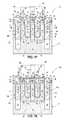
- FIG. 1is a diagrammatic cross-sectional view of a portion of an array of memory cells in process in accordance with an embodiment of the invention, and is taken through line 1 - 1 in FIG. 2 .
- FIG. 2is a cross-sectional view taken through line 2 - 2 in FIG. 1 .
- FIG. 3is a view of the FIG. 2 construction at a processing step subsequent to that shown by FIG. 2 .
- FIG. 4is a view of the FIG. 3 construction at a processing step subsequent to that shown by FIG. 3 .
- FIG. 5is an enlarged view of a portion of the FIG. 4 construction at a processing step subsequent to that shown by FIG. 4 .
- FIG. 6is a view of the FIG. 4 construction at a processing step subsequent to that shown by FIG. 5 .
- FIG. 7is an enlarged view of a portion of the FIG. 6 construction.
- FIG. 8is a view of the FIG. 4 construction at an alternate processing step subsequent to that shown by FIG. 5 .
- FIG. 9is an enlarged view of a portion of the FIG. 8 construction.
- FIG. 10is a view of the FIG. 1 construction at a processing step subsequent to that shown by FIGS. 6 and 7 , and is taken through line 10 - 10 in FIG. 11 .
- FIG. 11is a cross-sectional view taken through line 1 . 1 - 11 in FIG. 10 .
- FIG. 12is an enlarged view of a portion of the FIG. 11 construction.
- FIG. 13is a view of the FIG. 10 construction at a processing step subsequent to that shown by FIG. 10 , and is taken through line 13 - 13 in FIG. 14 .
- FIG. 14is a cross-sectional view taken through line 14 - 14 in FIG. 13 .
- FIG. 15is a view of the FIG. 11 construction at an alternate processing step to that shown by FIG. 14 .
- FIG. 16is a view of the FIG. 13 construction at a processing step subsequent to that shown by FIG. 13 , and is taken through line 16 - 16 in FIG. 17 .
- FIG. 17is a hybrid schematic and cross-sectional view taken through line 17 - 17 in FIG. 16 .
- FIG. 18is a hybrid schematic and cross-sectional view of the FIG. 14 construction at an alternate processing step to that shown by FIG. 17 .
- Embodiments of the inventionencompass methods of forming a transistor and methods of forming an array of memory cells that individually comprise a transistor and a capacitor (i.e., at least one transistor and at least one capacitor).
- an example construction 10comprises a base substrate 11 that may include one or more of conductive/conductor/conducting (i.e., electrically herein), semiconductive/semiconductor semiconducting, or insulative/insulator/insulating (i.e., electrically herein) materials.
- conductive/conductor/conductingi.e., electrically herein
- semiconductive/semiconductor semiconductingi.e., electrically herein
- insulative/insulator/insulatingi.e., electrically herein
- Example base substrate 11comprises suitably doped semiconductor material 12 (e.g., monocrystalline silicon) that in part functions as a channel of transistors.
- Masking material 22(e.g., thin silicon dioxide atop semiconductor material 12 and thicker silicon nitride atop the silicon dioxide) has been formed directly on semiconductor material 12 . Such is shown as having been patterned (e.g. using photolithography) and subsequently used as a mask in forming trenches 20 into semiconductor material 12 . Pitch multiplication may be used.
- the FIG. 2 cross-sectionshows trenches 20 passing over trench isolation 33 (e.g., one or both of silicon nitride and silicon dioxide) of the two laterally-outermost trenches 20 .
- An example depth of trenches 20 from the depicted tops 15 of semiconductor material 12 to the bases of trench isolation 33is 2,000 to 3,000 Angstroms.
- Recessed-access-gate-line constructions 14 a, 14 bhave been formed within semiconductor material 12 , for example within trenches 20 as shown.
- Example individual constructions 14 a, 14 bcomprise conductive gate material 16 having an elevationally-outermost surface 24 .
- Example materials 16include elemental metals (e.g., tungsten, titanium, copper, etc.), metal material (e.g., metal nitrides, metal silicide's, metal carbides, etc.), and conductively-doped-semiconductive materials (e.g., silicon, gallium, etc.), including mixtures thereof.
- Gate insulator material 18e.g., silicon dioxide and/or high k dielectrics is aside conductive gate material 16 .
- Example thickness for conductive gate material 16 where directly above semiconductor material 12is 800 to 1,200 Angstroms.
- Example thickness for gate insulator 18is 50 to 90 Angstroms.
- Recessed-access-gate-line constructions 14 a, 14 bmay be considered as individually comprising sides 17 and 19 , for example in the depicted FIG. 2 cross-section. Elevationally-outermost surface 24 of conductive gate material 16 is lower than elevationally-outermost surface 15 of semiconductor material 12 that is aside and above both sides 17 and 19 of an individual recessed-access-gate-line construction 14 a, 14 b.
- Recessed-access-gate-line constructions 14 a, 14 bmay be considered as comprising individual pairs 14 a / 14 b that are laterally-spaced relative one another (e.g., in vertical cross-sections along and parallel to line 2 - 2 in FIG. 1 ). Pairs 14 a / 14 b individually comprise a digit-line-contact region 26 laterally-inward between constructions 14 a and 14 b of the pair and a capacitor-contact region 28 laterally-outward of each of constructions 14 a and 14 b of the pair.
- Semiconductor material 12 that is above both sides 17 and 19 of individual recessed-access-gate line constructions 14 a, 14 bmay be considered as individually comprising two opposing sidewall surfaces 21 and 23 .
- One set of sidewalls surfaces 21 and 23may be considered as a pair 21 / 23 , with thereby there being two pairs 21 / 23 of two opposing sidewall surfaces 21 and 23 above both sides 17 and 19 of individual recessed-access-gate line constructions 14 .
- gate insulator material 18also extends elevationally along sidewall surfaces 21 and 23 .
- Example length of individual sidewall surfaces 21 and 23 above materials 18 and 30is 400 to 800 Angstroms.
- masking material 30(e.g., silicon dioxide) has been formed within trenches 20 atop conductive gate material 16 .
- masking material 30has been formed laterally over two facing sidewall surfaces 23 , 21 of semiconductor material 12 that is above both sides 17 and 19 of gate construction 14 .
- Such two facing sidewall surfaces 23 and 21individually are a different one of two opposing sidewall surfaces from a different one of two pairs 21 / 23 .
- such an individual sidewall 23is one from one pair 21 / 23 (e.g., the left-depicted pair) and an individual other sidewall 21 is one from another pair 21 / 23 (e.g., the right-depicted pair).
- masking material 30is formed laterally aside gate insulator material 18 that extends elevationally along such two facing sidewalls surfaces 23 and 21 .
- masking material 30has been elevationally recessed to leave top 24 of conductive gate material 16 covered by masking material 30 .
- gate insulator 18has been elevationally recessed.
- An example technique for such elevationally recessingis chemical etching using one or more etching chemistries depending upon the composition(s) of materials 30 and 18 .
- materials 30 and 18are of the same composition relative one another and the elevationally recessing of such materials occurs by chemical etching such materials at the same time.
- masking material 22 atop semiconductor material 12 and masking material 30 atop conductive gate material 16are formed to comprise different compositions relative one another (e.g., at least an outer portion of masking material 22 being silicon nitride and materials 18 and 30 being silicon dioxide). In one such embodiment and as shown, the chemical etching has been conducted selectively relative to masking material 22 that is atop semiconductor material 12 . Regardless, in one embodiment, gate insulator material 18 and masking material 30 after the act of elevationally recessing such materials have elevationally-outermost surfaces 32 and 34 , respectively, that are at a common elevation relative one another above conductive gate material 16 .
- Example thickness of materials 18 and 30 above conductive gate material 16is 30 to 100 Angstroms. One or both of materials 18 and 30 above conductive gate material 16 may at some point be sacrificial.
- tops 15 of semiconductor material 12 and top 24 of individual regions of conductive gate material 16have been covered with masking material 22 , 30 .
- Two pairs 21 / 23 of two opposing sidewall surfaces 21 and 23 of semiconductor material 12 in FIG. 4are laterally exposed above both sides 17 and 19 of individual recessed-access-gate-line constructions 14 a, 14 b.
- such act of covering tops 15 and top 24occurs over different time-space periods of time, and in one embodiment as shown and described wherein tops 15 of semiconductor material 12 have been covered with masking material 22 before the covering of tops 24 of conductive gate material 16 with masking material 30 .
- the act of coveringforms masking material 22 atop semiconductor material 12 and masking material 30 atop conductive gate material 16 to comprise different compositions relative one another.
- FIG. 5is a diagrammatic enlarged portion of FIG. 4 and shows processing occurring subsequently to that described above for FIG. 4 .
- a dopant monolayer 38has been formed directly on each of laterally-exposed two opposing sidewall surfaces 21 and 23 of each of two pairs 21 / 23 above both sides 17 and 19 of individual recessed-access-gate-line constructions 14 a, 14 b.
- dopant monolayers 38 and the methodcomprises monolayer doping whereby by definition dopant monolayers 38 are individually formed as a self-assembled covalently-bonded dopant-containing monolayer and directly on each of laterally exposed two opposing sidewall surfaces 21 and 23 of each of two pairs 21 / 23 , for example as shown.
- example dopant monolayers 38are individually diagrammatically shown as comprising individual molecules comprising a species Z and a species X bonded relative one another, with species X being covalently bonded to surface 21 or 23 .
- surfaces 21 and 23may be exposed to dilute HF at room temperature to remove any native oxide and leave a positively-charged surface.
- Surfaces 21 and 23may then be exposed to an organic dopant-containing source/precursor and mesitylene as a solvent. (from 4:1 to 25:1 by volume solvent to source/precursor) for 2.5 hours at 120° C. to form individual monolayers 38 .
- Diethyl 1-propylphosphonateis an example P dopant source
- a lylboronic acid pinacol esteris an example B dopant source
- triallylarsineis an example As dopant source.
- individual dopant monolayers 38may be formed by atomic layer deposition to include some conductivity-modifying dopant formed as a monolayer analogous to or the same as monolayer 38 or formed as a plurality (i.e., at least two) of stacked monolayers (not shown).
- a covering material 40in one embodiment which is dielectric (e.g., SiO 2 ), has been formed directly on dopant monolayers 38 .
- FIGS. 6 and 7show an example embodiment wherein covering material 40 completely fills space between immediately-adjacent projections of semiconductor material 12 .
- the covering materialmay be formed to less-than-fill such spaces, for example as is shown as covering material 40 d with respect to an alternate construction 10 d in FIGS. 8 and 9 .
- Like numerals from the above-described embodimentshave been used where appropriate, with some construction differences being indicated with the suffix “d”. Any other attribute(s) or aspect(s) as shown and/or described herein with respect to other embodiments may be used.
- dopantse.g., indicated by species X, and which may be only a portion of species X
- dopantshave been diffused (e.g., by rapid thermal anneal for 5 seconds at 950° C. or above) from dopant monolayers 38 having covering material 40 thereon (when present) into semiconductor material 12 that is above both sides 17 and 19 of individual recessed-access-gate-line constructions 14 a, 14 b through each of two opposing sidewall surfaces 21 and 23 of each of two pairs 21 / 23 .
- FIGS. 10-12diagrammatically show the diffused dopants as initially forming respective annuli 42 .
- Subsequent heating/annealingthat is one or both of inherent in subsequent processing or as a dedicated step (e.g., at 300° C. or greater for at least 30 minutes) results in likely complete lateral diffusion of the dopants (e.g., annuli 42 disappear), and forming there-from doped source/drain regions 44 and 45 as shown in FIGS. 13 and 14 above both sides 17 and 19 of individual recessed-access-gate-line constructions 14 a, 14 b.
- Individual source/drain regions 44are laterally-inward between recessed-access-gate-line constructions 14 a and 14 b of individual pairs 14 a / 14 b of the recessed-access-gate-line constructions and comprise individual digit-line-contact regions 26 .
- Source/drain regions 45are laterally-outward of each of recessed-access-gate-line constructions 14 a and 14 b of individual pairs 14 a / 14 b to comprise individual capacitor-contact regions 28 . Individual transistors 75 are thereby formed (only two being shown with outlines in FIGS. 13 and 14 for clarity). Semiconductor material 12 below source/drain regions 44 , 45 and around the bottom of constructions 14 a, 14 b functions as switchable channel material depending on voltage of conductive gate material 16 .
- FIGS. 13 and 14all of covering material 40 (not shown) has been removed after the diffusing shown by FIGS. 10-12 .
- Dielectric material 48has subsequently been deposited atop gate constructions 14 and source/drain regions 44 and 45 .
- at least some of a dielectric covering material 40may not be removed after the act of diffusing the dopants and which remains as part of a finished circuit construction that comprises the transistor.
- none of the dielectric covering materialis removed after the diffusing.
- FIG. 15shows such an example embodiment and construction 10 e wherein all of dielectric covering material 40 as shown in FIG. 6 remains, with dielectric material 48 e having been formed thereover.
- Like numerals from the above described embodimentshave been used where appropriate, with some construction differences being indicated with the suffix “e”. Any other attribute(s) or aspect(s) as shown and/or described herein with respect to other embodiments may be used
- capacitors 60are formed which individually electrically couple, in one embodiment directly electrically couple, to individual capacitor-contact regions 28 .
- Digit lines 70have been formed which individual electrically couple, in one embodiment directly electrically couple, to individual digit-line-contact regions 26 .
- Digit lines 70are schematically shown in FIG. 17 and example outlines thereof are diagrammatically shown in FIG. 16 .
- Capacitors 60may be formed above, below, or laterally-overlapping with digit lines 70 .
- example individual memory cells 80are formed that individually comprise a transistor 75 and a capacitor 60 . Other constructions may result.
- first conductive viasare formed which individually directly electrically couple individual capacitors 60 to individual capacitor-contact regions 28 .
- individual second conductive viasare formed which individually directly electrically couple individual digit lines 70 to individual digit-line-contact regions 26 .
- first conductive vias 62are shown as vertical schematic extensions as part of or from capacitors 60 and which directly electrically couple with individual capacitor-contact regions 28 .
- second conductive vias 72are shown as vertical schematic extensions of or from digit lines 70 .
- At least one of (a) first conductive vias 62 and (b) second conductive vias 72are directly against respective tops 15 of their individual capacitor-contact region 28 or individual digit-line-contact region 28 , with both (a) and (b) being so-directly against as shown in FIG. 17 .
- Construction 10 fhas at least one of (in one embodiment both of, as shown) (a) first conductive vias 62 f and (b) second conductive vias 72 f directly against a respective sidewall (e.g., a sidewall 21 or 23 ) of their individual capacitor contact region 26 or individual digit-line-contact region 28 .
- An embodiment of the inventioncomprises a method of forming a transistor (e.g., 75 ) comprising forming a gate construction (e.g., 14 a or 14 b ) having an elevationally-outermost surface (e.g., 24 ) of conductive gate material (e.g., 16 ) that is lower than an elevationally-outer surface 15 ), in one embodiment an elevationally-outermost surface (e.g., 15 ), of semiconductor material (e.g., 12 ) that is aside and above both sides (e.g., 17 and 19 ) of the gate construction.
- a gate constructione.g., 14 a or 14 b
- an elevationally-outermost surfacee.g., 24
- semiconductor materiale.g., 12
- Tops of the semiconductor material (e.g., tops 15 ) and the conductive gate material (e.g., top 24 )are covered with masking material (e.g., 22 / 30 ).
- Two pairs (e.g., two 21 / 23 's) of two opposing sidewall surfaces (e.g., 21 and 23 ) of the semiconductor materialare laterally exposed above both of the sides of the gate construction.
- the semiconductor material that is above both of the sides of the gate constructionis subjected to monolayer doping through each of the laterally-exposed two opposing sidewall surfaces of each of the two pairs and doped source/drain regions (e.g., 44 and 45 ) are formed there-from above both of the sides of the gate construction.
- a method of forming a transistorcomprises forming a gate construction (e.g., 14 a or 14 b ) having an elevationally outermost surface (e.g., 24 ) of conductive gate material (e.g., 16 ) that is lower than an elevationally-outermost surface (e.g., 15 ) of semiconductor material (e.g., 12 ) that is aside and above both sides (e.g., 17 and 19 ) of the gate construction.
- the semiconductor material that is above both of the sides of the gate constructionis subjected to monolayer doping and doped source/drain regions (e.g., 44 and 45 ) are formed there-from above both of the sides of the gate construction.
- the monolayer dopingis conducted in a vertically-self-aligned manner through two pairs (e.g., 21 / 23 ) of opposing sidewall surfaces (e.g., 21 and 23 ) of the semiconductor material that is above both of the sides of the gate construction.
- a method of forming a transistorcomprises forming a gate construction (e.g., 14 a or 14 b ) having an elevationally-outermost surface (e.g., 24 ) of conductive gate material (e.g., 16 ) that is lower than an elevationally-outer surface (e.g., 15 ) of semiconductor material (e.g., 12 ) that is aside and above both sides (e.g., 17 and 19 ) of the gate construction. Tops of the semiconductor material (e.g., tops 15 ) and the conductive gate material (e.g., top 24 ) are covered with masking material.
- Two pairs (e.g., two 21 / 23 's) of two opposing sidewall surfaces (e.g., 21 and 23 ) of the semiconductor materialare laterally exposed above both of the sides of the gate construction.
- a dopant monolayer (e.g., 38 )is formed directly on each of the laterally-exposed two opposing sidewall surfaces of each of the two pairs.
- a covering materiale.g., 40 or 40 d ) is formed directly on the dopant monolayers.
- Dopantsare diffused from the dopant monolayers having the covering material thereon into the semiconductor material that is above both of the sides of the gate construction through each of the two opposing sidewall surfaces of each of the two pairs and doped source/drain regions (e.g., 44 and 45 ) are formed there-from above both of the sides of the gate construction.
- Embodiments of the inventionmay achieve one or more advantages. For example, embodiments of the invention may be conducted without any ion implantation of dopant in forming source/drain regions, thereby reducing, minimizing, or eliminating defects and/or crystal lattice damage. Additionally, embodiments of the invention may form source/drain regions that are vertically-self-aligned accurately above the transistor gate thereby reducing, minimizing, or eliminating gate induced drain leakage. Additionally, as diameter of an elevationally-projecting cylindrical mass of semiconductor material decreases, the ratio of its area to volume increases, which may lead to more uniform doping of source/drain regions using embodiments of the invention.
- “monolayer doping”is defined as the formation of a self-assembled covalently-bonded dopant-containing monolayer directly on the surface of crystalline semiconductor material followed by annealing to thermally diffuse dopant atoms from the dopant-containing monolayer into the crystalline semiconductor material.
- “elevational”, “higher”, “upper”, “lower”, “top”, “atop”, “bottom”, “above”, “below”, “under”, “beneath”, “up”, and “down”are generally with reference to the vertical direction.
- “Horizontal”refers to a general direction (i.e., within 10 degrees) along a primary substrate surface and may be relative to which the substrate is processed during fabrication, and vertical is a direction generally orthogonal thereto.
- Reference to “exactly horizontal”is the direction along the primary substrate surface (i.e., no degrees there-from) and may be relative to which the substrate is processed during fabrication.
- “vertical” and “horizontal” as used hereinare generally perpendicular directions relative one another and independent of orientation of the substrate in three-dimensional space.
- “elevationally-extending” and “extending elevationally”refer to a direction that is angled away by at least 45° from exactly horizontal.
- “extend(ing) elevationally” and “elevationally-extending” with respect to a field effect transistorare with reference to orientation of the transistor's channel length along which current flows in operation between the source/drain regions.
- “extend(ing) elevationally” and “elevationally-extending”are with reference to orientation of the base length along which current flows in operation between the emitter and collector.
- any of the materials, regions, and structures described hereinmay be homogenous or non-homogenous, and regardless may be continuous or discontinuous over any material which such overlie. Further, unless otherwise stated, each material may be formed using any suitable or yet-to-be-developed technique, with atomic layer deposition, chemical vapor deposition, physical vapor deposition, epitaxial growth, diffusion doping, and ion implanting being examples.
- thicknessby itself (no preceding directional adjective) is defined as the mean straight-line distance through a given material or region perpendicularly from a closest surface of an immediately-adjacent material of different composition or of an immediately-adjacent region.
- various materials or regions described hereinmay be of substantially constant thickness or of variable thicknesses. If of variable thickness, thickness refers to average thickness unless otherwise indicated, and such material or region will have some minimum thickness and some maximum thickness due to the thickness being variable.
- different compositiononly requires those portions of two stated materials or regions that may be directly against one another to be chemically and/or physically different, for example if such materials or regions are not homogenous.
- “different composition”only requires that those portions of the two stated materials or regions that are closest to one another be chemically and/or physically different if such materials or regions are not homogenous.
- a material, region, or structureis “directly against” another when there is at least some physical touching contact of the stated materials, regions, or structures relative one another.
- “over”, “on”, “adjacent”, “along”, and “against” not preceded by “directly”encompass “directly against” as well as construction where intervening material(s), region(s), or structure(s) result(s) in no physical touching contact of the stated materials, regions, or structures relative one another.
- regions-materials-componentsare “electrically coupled” relative one another if in normal operation electric current is capable of continuously flowing from one to the other, and does so predominately by movement of subatomic positive and/or negative charges when such are sufficiently generated.
- Another electronic componentmay be between and electrically coupled to the regions-materials-components.
- regions-materials-componentsare referred to as being “directly electrically coupled”, no intervening electronic component (e.g., no diode, transistor, resistor, transducer, switch, fuse, etc.) is between the directly electrically coupled regions-materials-components.
- metal materialis any one or combination of an elemental metal, a mixture or an alloy of two or more elemental metals, and any conductive metal compound.
- etch, etching, removing, removal, forming, and/or formationis such an act of one stated material relative to another stated material(s) so acted upon at a rate of at least 2:1 by volume.
- a “vertically-self-aligned manner”means a technique whereby length and position of some or all of an elevationally-extending feature (e.g., a source/drain region) is formed by previously-defined top and bottom termini of an elevationally-extending sidewall or a portion thereof of said feature, thereby not requiring subsequent processing with respect to those top and bottom termini, and with the technique being selective to formation of the feature on and/or through said sidewall or portion thereof (i.e., selective to formation on and/or through said sidewall or portion thereof relative to horizontal surfaces and selective to formation on and/or through said sidewall or portion thereof relative to other elevationally-extending surfaces).
- an elevationally-extending featuree.g., a source/drain region
Landscapes
- Engineering & Computer Science (AREA)
- Microelectronics & Electronic Packaging (AREA)
- Computer Hardware Design (AREA)
- Semiconductor Memories (AREA)
Abstract
Description
- Embodiments disclosed herein pertain to methods of forming a transistor and to methods of forming an array of memory cells.
- Memory is one type of integrated circuitry, and is used in computer systems for storing data. Memory may he fabricated in one or more arrays of individual memory cells. Memory cells may be written to, or read from, using digit lines (which may also be referred to as hit lines, data lines, or sense lines) and access lines (which may also be referred to as word lines). The sense lines may conductively interconnect memory cells along columns of the array, and the access lines may conductively interconnect memory cells along rows of the array. Each memory cell may be uniquely addressed through the combination of a sense line and an access line.
- Memory cells may be volatile, semi-volatile, or non-volatile. Non-volatile memory cells can store data for extended periods of time in the absence of power. Non-volatile memory is conventionally specified to be memory having a retention time of at least about 10 years. Volatile memory dissipates, and is therefore refreshed/rewritten to maintain data storage. Volatile memory may have a retention time of milliseconds or less. Regardless, memory cells are configured to retain or store memory in at least two different selectable states. In a binary system, the states are considered as either a “0” or a “1”. In other systems, at least some individual memory cells may be configured to store more than two levels or states of information.
- A field effect transistor is one type of electronic component that may be used in a memory cell. These transistors comprise a pair of conductive source/drain regions having a semiconductive channel region there-between. A conductive gate is adjacent the channel region and separated there-from by a thin gate insulator. Application of a suitable voltage to the gate allows current to flow from one of the source/drain regions to the other through the channel region. When the voltage is removed from the gate, current is largely prevented from flowing through the channel region. Field effect transistors may also include additional structure, for example a reversibly programmable charge-storage region as part of the gate construction between the gate insulator and the conductive gate.
- Transistors may be used in circuitry other than memory circuitry.
FIG. 1 is a diagrammatic cross-sectional view of a portion of an array of memory cells in process in accordance with an embodiment of the invention, and is taken through line1-1 inFIG. 2 .FIG. 2 is a cross-sectional view taken through line2-2 inFIG. 1 .FIG. 3 is a view of theFIG. 2 construction at a processing step subsequent to that shown byFIG. 2 .FIG. 4 is a view of theFIG. 3 construction at a processing step subsequent to that shown byFIG. 3 .FIG. 5 is an enlarged view of a portion of theFIG. 4 construction at a processing step subsequent to that shown byFIG. 4 .FIG. 6 is a view of theFIG. 4 construction at a processing step subsequent to that shown byFIG. 5 .FIG. 7 is an enlarged view of a portion of theFIG. 6 construction.FIG. 8 is a view of theFIG. 4 construction at an alternate processing step subsequent to that shown byFIG. 5 .FIG. 9 is an enlarged view of a portion of theFIG. 8 construction.FIG. 10 is a view of theFIG. 1 construction at a processing step subsequent to that shown byFIGS. 6 and 7 , and is taken through line10-10 inFIG. 11 .FIG. 11 is a cross-sectional view taken through line1.1-11 inFIG. 10 .FIG. 12 is an enlarged view of a portion of theFIG. 11 construction.FIG. 13 is a view of theFIG. 10 construction at a processing step subsequent to that shown byFIG. 10 , and is taken through line13-13 inFIG. 14 .FIG. 14 is a cross-sectional view taken through line14-14 inFIG. 13 .FIG. 15 is a view of theFIG. 11 construction at an alternate processing step to that shown byFIG. 14 .FIG. 16 is a view of theFIG. 13 construction at a processing step subsequent to that shown byFIG. 13 , and is taken through line16-16 inFIG. 17 .FIG. 17 is a hybrid schematic and cross-sectional view taken through line17-17 inFIG. 16 .FIG. 18 is a hybrid schematic and cross-sectional view of theFIG. 14 construction at an alternate processing step to that shown byFIG. 17 .- Embodiments of the invention encompass methods of forming a transistor and methods of forming an array of memory cells that individually comprise a transistor and a capacitor (i.e., at least one transistor and at least one capacitor).
- Referring to
FIGS. 1 and 2 , anexample construction 10 comprises abase substrate 11 that may include one or more of conductive/conductor/conducting (i.e., electrically herein), semiconductive/semiconductor semiconducting, or insulative/insulator/insulating (i.e., electrically herein) materials. Various materials have been formed abovebase substrate 11. Materials may be aside, elevationally inward of, or elevationally outward of theFIGS. 1 and 2 —depicted materials. For example, other partially or wholly fabricated components of integrated circuitry may be provided somewhere above, about, or withinbase substrate 11. Control and/or other peripheral circuitry for operating components within an array of memory cells may also be fabricated, and may or may not be wholly or partially within an array or sub-array. Further, multiple sub-arrays may also be fabricated and operated independently, in tandem, or otherwise relative one another. As used in this document, a “sub-array” may also be considered as an array.Example base substrate 11 comprises suitably doped semiconductor material12 (e.g., monocrystalline silicon) that in part functions as a channel of transistors. - Masking material22 (e.g., thin silicon dioxide atop
semiconductor material 12 and thicker silicon nitride atop the silicon dioxide) has been formed directly onsemiconductor material 12. Such is shown as having been patterned (e.g. using photolithography) and subsequently used as a mask in formingtrenches 20 intosemiconductor material 12. Pitch multiplication may be used. TheFIG. 2 cross-section showstrenches 20 passing over trench isolation33 (e.g., one or both of silicon nitride and silicon dioxide) of the two laterally-outermost trenches 20. An example depth oftrenches 20 from the depictedtops 15 ofsemiconductor material 12 to the bases oftrench isolation 33 is 2,000 to 3,000 Angstroms. - Recessed-access-gate-
line constructions semiconductor material 12, for example withintrenches 20 as shown. Exampleindividual constructions conductive gate material 16 having an elevationally-outermost surface 24.Example materials 16 include elemental metals (e.g., tungsten, titanium, copper, etc.), metal material (e.g., metal nitrides, metal silicide's, metal carbides, etc.), and conductively-doped-semiconductive materials (e.g., silicon, gallium, etc.), including mixtures thereof. Gate insulator material18 (e.g., silicon dioxide and/or high k dielectrics) is asideconductive gate material 16. Example thickness forconductive gate material 16 where directly above semiconductor material12 (e.g., the two laterally-middle constructions FIG. 3 ) is 800 to 1,200 Angstroms. Example thickness forgate insulator 18 is 50 to 90 Angstroms. Recessed-access-gate-line constructions sides FIG. 2 cross-section. Elevationally-outermost surface 24 ofconductive gate material 16 is lower than elevationally-outermost surface 15 ofsemiconductor material 12 that is aside and above bothsides line construction - Recessed-access-gate-
line constructions individual pairs 14a/14bthat are laterally-spaced relative one another (e.g., in vertical cross-sections along and parallel to line2-2 inFIG. 1 ).Pairs 14a/14bindividually comprise a digit-line-contact region 26 laterally-inward betweenconstructions contact region 28 laterally-outward of each ofconstructions Semiconductor material 12 that is above bothsides access-gate line constructions pair 21/23, with thereby there being twopairs 21/23 of two opposing sidewall surfaces21 and23 above bothsides access-gate line constructions 14. Regardless, in one embodiment and as shown,gate insulator material 18 also extends elevationally along sidewall surfaces21 and23. Example length of individual sidewall surfaces21 and23 abovematerials - Referring to
FIG. 3 , masking material30 (e.g., silicon dioxide) has been formed withintrenches 20 atopconductive gate material 16. In one embodiment and as shown, maskingmaterial 30 has been formed laterally over two facing sidewall surfaces23,21 ofsemiconductor material 12 that is above bothsides gate construction 14. Such two facing sidewall surfaces23 and21 individually are a different one of two opposing sidewall surfaces from a different one of twopairs 21/23. For example, and as shown, such anindividual sidewall 23 is one from onepair 21/23 (e.g., the left-depicted pair) and an individualother sidewall 21 is one from anotherpair 21/23 (e.g., the right-depicted pair). In one embodiment and as shown, maskingmaterial 30 is formed laterally asidegate insulator material 18 that extends elevationally along such two facing sidewalls surfaces23 and21. - Referring to
FIG. 4 , maskingmaterial 30 has been elevationally recessed to leave top24 ofconductive gate material 16 covered by maskingmaterial 30. Further, in one embodiment and as shown,gate insulator 18 has been elevationally recessed. An example technique for such elevationally recessing is chemical etching using one or more etching chemistries depending upon the composition(s) ofmaterials materials material 22 atopsemiconductor material 12 and maskingmaterial 30 atopconductive gate material 16 are formed to comprise different compositions relative one another (e.g., at least an outer portion of maskingmaterial 22 being silicon nitride andmaterials material 22 that is atopsemiconductor material 12. Regardless, in one embodiment,gate insulator material 18 and maskingmaterial 30 after the act of elevationally recessing such materials have elevationally-outermost surfaces conductive gate material 16. Example thickness ofmaterials conductive gate material 16 is 30 to 100 Angstroms. One or both ofmaterials conductive gate material 16 may at some point be sacrificial. - The above example processings are example techniques whereby tops15 of
semiconductor material 12 and top24 of individual regions ofconductive gate material 16 have been covered with maskingmaterial pairs 21/23 of two opposing sidewall surfaces21 and23 ofsemiconductor material 12 inFIG. 4 are laterally exposed above bothsides line constructions semiconductor material 12 have been covered with maskingmaterial 22 before the covering oftops 24 ofconductive gate material 16 with maskingmaterial 30. Regardless, in one embodiment and as described above, the act of coveringforms masking material 22 atopsemiconductor material 12 and maskingmaterial 30 atopconductive gate material 16 to comprise different compositions relative one another. FIG. 5 is a diagrammatic enlarged portion ofFIG. 4 and shows processing occurring subsequently to that described above forFIG. 4 . Specifically, adopant monolayer 38 has been formed directly on each of laterally-exposed two opposing sidewall surfaces21 and23 of each of twopairs 21/23 above bothsides line constructions dopant monolayers 38 and the method comprises monolayer doping whereby bydefinition dopant monolayers 38 are individually formed as a self-assembled covalently-bonded dopant-containing monolayer and directly on each of laterally exposed two opposing sidewall surfaces21 and23 of each of twopairs 21/23, for example as shown. Specifically,example dopant monolayers 38 are individually diagrammatically shown as comprising individual molecules comprising a species Z and a species X bonded relative one another, with species X being covalently bonded to surface21 or23. For example, and by way or examples only, surfaces21 and23 may be exposed to dilute HF at room temperature to remove any native oxide and leave a positively-charged surface.Surfaces individual monolayers 38. Diethyl 1-propylphosphonate is an example P dopant source, a lylboronic acid pinacol ester is an example B dopant source, and triallylarsine is an example As dopant source.- Alternately and by way of example only,
individual dopant monolayers 38 may be formed by atomic layer deposition to include some conductivity-modifying dopant formed as a monolayer analogous to or the same asmonolayer 38 or formed as a plurality (i.e., at least two) of stacked monolayers (not shown). - Referring to
FIGS. 6 and 7 , and in one embodiment, a coveringmaterial 40, in one embodiment which is dielectric (e.g., SiO2), has been formed directly ondopant monolayers 38.FIGS. 6 and 7 show an example embodiment wherein coveringmaterial 40 completely fills space between immediately-adjacent projections ofsemiconductor material 12. Alternately, the covering material may be formed to less-than-fill such spaces, for example as is shown as coveringmaterial 40dwith respect to analternate construction 10dinFIGS. 8 and 9 . Like numerals from the above-described embodiments have been used where appropriate, with some construction differences being indicated with the suffix “d”. Any other attribute(s) or aspect(s) as shown and/or described herein with respect to other embodiments may be used. - Referring to
FIGS. 10-12 , dopants (e.g., indicated by species X, and which may be only a portion of species X) have been diffused (e.g., by rapid thermal anneal for 5 seconds at 950° C. or above) fromdopant monolayers 38 havingcovering material 40 thereon (when present) intosemiconductor material 12 that is above bothsides line constructions pairs 21/23.FIGS. 10-12 diagrammatically show the diffused dopants as initially formingrespective annuli 42. - Subsequent heating/annealing that is one or both of inherent in subsequent processing or as a dedicated step (e.g., at 300° C. or greater for at least 30 minutes) results in likely complete lateral diffusion of the dopants (e.g.,
annuli 42 disappear), and forming there-from doped source/drain regions FIGS. 13 and 14 above bothsides line constructions drain regions 44 are laterally-inward between recessed-access-gate-line constructions individual pairs 14a/14bof the recessed-access-gate-line constructions and comprise individual digit-line-contact regions 26. Source/drain regions 45 are laterally-outward of each of recessed-access-gate-line constructions individual pairs 14a/14bto comprise individual capacitor-contact regions 28.Individual transistors 75 are thereby formed (only two being shown with outlines inFIGS. 13 and 14 for clarity).Semiconductor material 12 below source/drain regions constructions conductive gate material 16. - In one embodiment and as shown in
FIGS. 13 and 14 , all of covering material40 (not shown) has been removed after the diffusing shown byFIGS. 10-12 .Dielectric material 48 has subsequently been deposited atopgate constructions 14 and source/drain regions dielectric covering material 40 may not be removed after the act of diffusing the dopants and which remains as part of a finished circuit construction that comprises the transistor. In one such embodiment, none of the dielectric covering material is removed after the diffusing.FIG. 15 shows such an example embodiment andconstruction 10ewherein all ofdielectric covering material 40 as shown inFIG. 6 remains, withdielectric material 48e having been formed thereover. Like numerals from the above described embodiments have been used where appropriate, with some construction differences being indicated with the suffix “e”. Any other attribute(s) or aspect(s) as shown and/or described herein with respect to other embodiments may be used - Referring to
FIGS. 16 and 17 , after the act of diffusing the dopants,capacitors 60 are formed which individually electrically couple, in one embodiment directly electrically couple, to individual capacitor-contact regions 28.Digit lines 70 have been formed which individual electrically couple, in one embodiment directly electrically couple, to individual digit-line-contact regions 26.Digit lines 70 are schematically shown inFIG. 17 and example outlines thereof are diagrammatically shown inFIG. 16 .Capacitors 60 may be formed above, below, or laterally-overlapping withdigit lines 70. Regardless, exampleindividual memory cells 80 are formed that individually comprise atransistor 75 and acapacitor 60. Other constructions may result. - In one embodiment, individual first conductive vias are formed which individually directly electrically couple
individual capacitors 60 to individual capacitor-contact regions 28. In one embodiment, individual second conductive vias are formed which individually directly electrically coupleindividual digit lines 70 to individual digit-line-contact regions 26. By way of examples and diagrammatically, firstconductive vias 62 are shown as vertical schematic extensions as part of or fromcapacitors 60 and which directly electrically couple with individual capacitor-contact regions 28. Additionally, example such secondconductive vias 72 are shown as vertical schematic extensions of or from digit lines70. In one embodiment, at least one of (a) firstconductive vias 62 and (b) secondconductive vias 72 are directly againstrespective tops 15 of their individual capacitor-contact region 28 or individual digit-line-contact region 28, with both (a) and (b) being so-directly against as shown inFIG. 17 . - An alternate example embodiment is shown in
FIG. 18 . Like numerals from the above-described embodiments have been used where appropriate, with some construction differences being indicated with the suffix “f”.Construction 10f has at least one of (in one embodiment both of, as shown) (a) firstconductive vias 62fand (b) second conductive vias72fdirectly against a respective sidewall (e.g., asidewall 21 or23) of their individualcapacitor contact region 26 or individual digit-line-contact region 28. - An embodiment of the invention comprises a method of forming a transistor (e.g.,75) comprising forming a gate construction (e.g.,14aor14b) having an elevationally-outermost surface (e.g.,24) of conductive gate material (e.g.,16) that is lower than an elevationally-outer surface15), in one embodiment an elevationally-outermost surface (e.g.,15), of semiconductor material (e.g.,12) that is aside and above both sides (e.g.,17 and19) of the gate construction. Tops of the semiconductor material (e.g., tops15) and the conductive gate material (e.g., top24) are covered with masking material (e.g.,22/30). Two pairs (e.g., two21/23's) of two opposing sidewall surfaces (e.g.,21 and23) of the semiconductor material are laterally exposed above both of the sides of the gate construction. After the covering, the semiconductor material that is above both of the sides of the gate construction is subjected to monolayer doping through each of the laterally-exposed two opposing sidewall surfaces of each of the two pairs and doped source/drain regions (e.g.,44 and45) are formed there-from above both of the sides of the gate construction.
- In one embodiment, a method of forming a transistor (e.g.,75) comprises forming a gate construction (e.g.,14aor14b) having an elevationally outermost surface (e.g.,24) of conductive gate material (e.g.,16) that is lower than an elevationally-outermost surface (e.g.,15) of semiconductor material (e.g.,12) that is aside and above both sides (e.g.,17 and19) of the gate construction. The semiconductor material that is above both of the sides of the gate construction is subjected to monolayer doping and doped source/drain regions (e.g.,44 and45) are formed there-from above both of the sides of the gate construction. The monolayer doping is conducted in a vertically-self-aligned manner through two pairs (e.g.,21/23) of opposing sidewall surfaces (e.g.,21 and23) of the semiconductor material that is above both of the sides of the gate construction.
- In one embodiment, a method of forming a transistor (e.g.,75) comprises forming a gate construction (e.g.,14aor14b) having an elevationally-outermost surface (e.g.,24) of conductive gate material (e.g.,16) that is lower than an elevationally-outer surface (e.g.,15) of semiconductor material (e.g.,12) that is aside and above both sides (e.g.,17 and19) of the gate construction. Tops of the semiconductor material (e.g., tops15) and the conductive gate material (e.g., top24) are covered with masking material. Two pairs (e.g., two21/23's) of two opposing sidewall surfaces (e.g.,21 and23) of the semiconductor material are laterally exposed above both of the sides of the gate construction. A dopant monolayer (e.g.,38) is formed directly on each of the laterally-exposed two opposing sidewall surfaces of each of the two pairs. A covering material (e.g.,40 or40d) is formed directly on the dopant monolayers. Dopants are diffused from the dopant monolayers having the covering material thereon into the semiconductor material that is above both of the sides of the gate construction through each of the two opposing sidewall surfaces of each of the two pairs and doped source/drain regions (e.g.,44 and45) are formed there-from above both of the sides of the gate construction.
- Embodiments of the invention may achieve one or more advantages. For example, embodiments of the invention may be conducted without any ion implantation of dopant in forming source/drain regions, thereby reducing, minimizing, or eliminating defects and/or crystal lattice damage. Additionally, embodiments of the invention may form source/drain regions that are vertically-self-aligned accurately above the transistor gate thereby reducing, minimizing, or eliminating gate induced drain leakage. Additionally, as diameter of an elevationally-projecting cylindrical mass of semiconductor material decreases, the ratio of its area to volume increases, which may lead to more uniform doping of source/drain regions using embodiments of the invention.
- In this document, “monolayer doping” is defined as the formation of a self-assembled covalently-bonded dopant-containing monolayer directly on the surface of crystalline semiconductor material followed by annealing to thermally diffuse dopant atoms from the dopant-containing monolayer into the crystalline semiconductor material.
- In this document unless otherwise indicated, “elevational”, “higher”, “upper”, “lower”, “top”, “atop”, “bottom”, “above”, “below”, “under”, “beneath”, “up”, and “down” are generally with reference to the vertical direction. “Horizontal” refers to a general direction (i.e., within 10 degrees) along a primary substrate surface and may be relative to which the substrate is processed during fabrication, and vertical is a direction generally orthogonal thereto. Reference to “exactly horizontal” is the direction along the primary substrate surface (i.e., no degrees there-from) and may be relative to which the substrate is processed during fabrication. Further, “vertical” and “horizontal” as used herein are generally perpendicular directions relative one another and independent of orientation of the substrate in three-dimensional space. Additionally, “elevationally-extending” and “extending elevationally” refer to a direction that is angled away by at least 45° from exactly horizontal. Further, “extend(ing) elevationally” and “elevationally-extending” with respect to a field effect transistor are with reference to orientation of the transistor's channel length along which current flows in operation between the source/drain regions. For bipolar junction transistors, “extend(ing) elevationally” and “elevationally-extending” are with reference to orientation of the base length along which current flows in operation between the emitter and collector.
- Further, “directly above” and “directly under” require at least some lateral overlap (i.e., horizontally) of two stated regions/materials/components relative one another. Also, use of “above” not preceded by “directly” only requires that some portion of the stated region/material/component that is above the other be elevationally outward of the other (i.e., independent of whether there is any lateral overlap of the two stated regions/materials/components). Analogously, use of “under” not preceded by “directly” only requires that some portion of the stated region/material/component that is under the other be elevationally inward of the other (i.e., independent of whether there is any lateral overlap of the two stated regions/material s/components).
- Any of the materials, regions, and structures described herein may be homogenous or non-homogenous, and regardless may be continuous or discontinuous over any material which such overlie. Further, unless otherwise stated, each material may be formed using any suitable or yet-to-be-developed technique, with atomic layer deposition, chemical vapor deposition, physical vapor deposition, epitaxial growth, diffusion doping, and ion implanting being examples.
- Additionally, “thickness” by itself (no preceding directional adjective) is defined as the mean straight-line distance through a given material or region perpendicularly from a closest surface of an immediately-adjacent material of different composition or of an immediately-adjacent region. Additionally, the various materials or regions described herein may be of substantially constant thickness or of variable thicknesses. If of variable thickness, thickness refers to average thickness unless otherwise indicated, and such material or region will have some minimum thickness and some maximum thickness due to the thickness being variable. As used herein, “different composition” only requires those portions of two stated materials or regions that may be directly against one another to be chemically and/or physically different, for example if such materials or regions are not homogenous. If the two stated materials or regions are not directly against one another, “different composition” only requires that those portions of the two stated materials or regions that are closest to one another be chemically and/or physically different if such materials or regions are not homogenous. In this document, a material, region, or structure is “directly against” another when there is at least some physical touching contact of the stated materials, regions, or structures relative one another. In contrast, “over”, “on”, “adjacent”, “along”, and “against” not preceded by “directly” encompass “directly against” as well as construction where intervening material(s), region(s), or structure(s) result(s) in no physical touching contact of the stated materials, regions, or structures relative one another.
- Herein, regions-materials-components are “electrically coupled” relative one another if in normal operation electric current is capable of continuously flowing from one to the other, and does so predominately by movement of subatomic positive and/or negative charges when such are sufficiently generated. Another electronic component may be between and electrically coupled to the regions-materials-components. In contrast, when regions-materials-components are referred to as being “directly electrically coupled”, no intervening electronic component (e.g., no diode, transistor, resistor, transducer, switch, fuse, etc.) is between the directly electrically coupled regions-materials-components.
- Additionally, “metal material” is any one or combination of an elemental metal, a mixture or an alloy of two or more elemental metals, and any conductive metal compound.
- In this document, “selective” as to etch, etching, removing, removal, forming, and/or formation is such an act of one stated material relative to another stated material(s) so acted upon at a rate of at least 2:1 by volume.
- In this document, a “vertically-self-aligned manner” means a technique whereby length and position of some or all of an elevationally-extending feature (e.g., a source/drain region) is formed by previously-defined top and bottom termini of an elevationally-extending sidewall or a portion thereof of said feature, thereby not requiring subsequent processing with respect to those top and bottom termini, and with the technique being selective to formation of the feature on and/or through said sidewall or portion thereof (i.e., selective to formation on and/or through said sidewall or portion thereof relative to horizontal surfaces and selective to formation on and/or through said sidewall or portion thereof relative to other elevationally-extending surfaces).
- In compliance with the statute, the subject matter disclosed herein has been described in language more or less specific as to structural and methodical features. It is to be understood, however, that the claims are not limited to the specific features shown and described, since the means herein disclosed comprise example embodiments. The claims are thus to be afforded full scope as literally worded, and to be appropriately interpreted in accordance with the doctrine of equivalents.
Claims (21)
Priority Applications (4)
| Application Number | Priority Date | Filing Date | Title |
|---|---|---|---|
| US15/843,493US10643906B2 (en) | 2017-12-15 | 2017-12-15 | Methods of forming a transistor and methods of forming an array of memory cells |
| CN201880063923.8ACN111164755B (en) | 2017-12-15 | 2018-10-11 | Method of forming transistor and method of forming memory cell array |
| PCT/US2018/055407WO2019118052A1 (en) | 2017-12-15 | 2018-10-11 | Methods of forming a transistor and methods of forming an array of memory cells |
| TW107137864ATWI675452B (en) | 2017-12-15 | 2018-10-26 | Methods of forming a transistor and methods of forming an array of memory cells |
Applications Claiming Priority (1)
| Application Number | Priority Date | Filing Date | Title |
|---|---|---|---|
| US15/843,493US10643906B2 (en) | 2017-12-15 | 2017-12-15 | Methods of forming a transistor and methods of forming an array of memory cells |
Publications (2)
| Publication Number | Publication Date |
|---|---|
| US20190189515A1true US20190189515A1 (en) | 2019-06-20 |
| US10643906B2 US10643906B2 (en) | 2020-05-05 |
Family
ID=66814686
Family Applications (1)
| Application Number | Title | Priority Date | Filing Date |
|---|---|---|---|
| US15/843,493Active2038-01-30US10643906B2 (en) | 2017-12-15 | 2017-12-15 | Methods of forming a transistor and methods of forming an array of memory cells |
Country Status (4)
| Country | Link |
|---|---|
| US (1) | US10643906B2 (en) |
| CN (1) | CN111164755B (en) |
| TW (1) | TWI675452B (en) |
| WO (1) | WO2019118052A1 (en) |
Families Citing this family (4)
| Publication number | Priority date | Publication date | Assignee | Title |
|---|---|---|---|---|
| JP2021150605A (en)* | 2020-03-23 | 2021-09-27 | キオクシア株式会社 | Semiconductor storage device and manufacturing method for the same |
| US11785762B2 (en)* | 2021-06-30 | 2023-10-10 | Micron Technology, Inc. | Memory circuitry and method used in forming memory circuitry |
| CN116471837B (en)* | 2023-03-16 | 2024-03-12 | 北京超弦存储器研究院 | Semiconductor structure, memory structure and preparation method thereof |
| TWI883767B (en)* | 2024-01-05 | 2025-05-11 | 力晶積成電子製造股份有限公司 | Trench type semiconductor device |
Citations (43)
| Publication number | Priority date | Publication date | Assignee | Title |
|---|---|---|---|---|
| US5854111A (en)* | 1997-03-27 | 1998-12-29 | United Microelectronics Corp. | ROM device using a schuckly diode |
| US20050179075A1 (en)* | 2004-02-13 | 2005-08-18 | Lee Jin-Woo | Transistors having a channel region between channel-portion holes and methods of forming the same |
| US20050189582A1 (en)* | 2004-02-10 | 2005-09-01 | Thomas Mikolajick | Charge trapping memory cell and fabrication method |
| US20070034922A1 (en)* | 2005-08-11 | 2007-02-15 | Micron Technology, Inc. | Integrated surround gate multifunctional memory device |
| US20070082448A1 (en)* | 2005-10-12 | 2007-04-12 | Samsung Electronics Co., Ltd. | Semiconductor devices having transistors with vertical channels and method of fabricating the same |
| US20070253233A1 (en)* | 2006-03-30 | 2007-11-01 | Torsten Mueller | Semiconductor memory device and method of production |
| US20090029520A1 (en)* | 2007-07-23 | 2009-01-29 | Samsung Electronics Co., Ltd. | Methods of forming semiconductor device |
| US20090294842A1 (en)* | 2008-05-30 | 2009-12-03 | Micron Technology, Inc. | Methods of forming data cells and connections to data cells |
| US20100066440A1 (en)* | 2008-09-15 | 2010-03-18 | Micron Technology, Inc. | Transistor with a passive gate and methods of fabricating the same |
| US20110217820A1 (en)* | 2010-03-02 | 2011-09-08 | Samsung Electronics Co., Ltd. | Methods of fabricating semiconductor devices |
| US20110298046A1 (en)* | 2010-06-04 | 2011-12-08 | Ki-Ro Hong | Semiconductor device with buried bit lines and method for fabricating the same |
| US20120018702A1 (en)* | 2010-07-26 | 2012-01-26 | The Regents Of The University Of California | Surface and gas phase doping of iii-v semiconductors |
| US20120126883A1 (en)* | 2010-11-19 | 2012-05-24 | Micron Technology,Inc. | Vertically stacked fin transistors and methods of fabricating and operating the same |
| US20120217570A1 (en)* | 2011-02-28 | 2012-08-30 | Hynix Semiconductor Inc. | Semiconductor memory device and method for manufacturing the same |
| US20130049072A1 (en)* | 2011-08-25 | 2013-02-28 | Lars P. Heineck | Arrays Of Recessed Access Devices, Methods Of Forming Recessed Access Gate Constructions, And Methods Of Forming Isolation Gate Constructions In The Fabrication Of Recessed Access Devices |
| US20130187207A1 (en)* | 2011-07-27 | 2013-07-25 | Advanced Ion Beam Technology, Inc. | Replacement source/drain finfet fabrication |
| US20130234230A1 (en)* | 2012-03-09 | 2013-09-12 | Kazuaki TAKESAKO | Semiconductor Device and Method for Making the Same |
| US20130299895A1 (en)* | 2012-05-09 | 2013-11-14 | Taiwan Semiconductor Manufacturing Co., Ltd. | Iii-v compound semiconductor device having dopant layer and method of making the same |
| US20130316513A1 (en)* | 2012-05-23 | 2013-11-28 | International Business Machines Corporation | Fin isolation for multigate transistors |
| US20140252475A1 (en)* | 2013-03-08 | 2014-09-11 | Taiwan Semiconductor Manufacturing Company, Ltd. | FinFETs and Methods for Forming the Same |
| US20150028406A1 (en)* | 2013-07-23 | 2015-01-29 | Micron Technology, Inc. | Arrays Of Recessed Access Gate Lines, Arrays Of Conductive Lines, Arrays Of Recessed Access Gate Lines And Conductive Lines, Memory Circuitry, Methods Of Forming An Array Of Recessed Access Gate Lines, Methods Of Forming An Array Of Conductive Lines, And Methods Of Forming An Array Of Recessed Access Gate Lines And An Array Of Conductive Lines |
| US20150243748A1 (en)* | 2014-02-26 | 2015-08-27 | Micron Technology, Inc. | Vertical access devices, semiconductor device structures, and related methods |
| US20160093732A1 (en)* | 2014-09-25 | 2016-03-31 | Inotera Memories, Inc. | Non-floating vertical transistor structure |
| US20160365411A1 (en)* | 2015-06-15 | 2016-12-15 | International Business Machines Corporation | Series resistance reduction in vertically stacked silicon nanowire transistors |
| US20170040449A1 (en)* | 2015-08-03 | 2017-02-09 | Semiwise Limited | Reduced Local Threshold Voltage Variation MOSFET Using Multiple Layers of Epi for Improved Device Operation |
| US9583489B1 (en)* | 2016-01-08 | 2017-02-28 | International Business Machines Corporation | Solid state diffusion doping for bulk finFET devices |
| US20170062575A1 (en)* | 2015-08-31 | 2017-03-02 | Samsung Electronics Co., Ltd. | Semiconductor device and method of fabricating the same |
| US20170162694A1 (en)* | 2015-12-03 | 2017-06-08 | International Business Machines Corporation | Transistor and method of forming same |
| US20170179031A1 (en)* | 2015-12-19 | 2017-06-22 | Micron Technology, Inc. | Electronic Component Of Integrated Circuitry And A Method Of Forming A Conductive Via To A Region Of Semiconductor Material |
| US20180025911A1 (en)* | 2016-07-20 | 2018-01-25 | Imec Vzw | Monolithic Integration of Semiconductor Materials |
| US9997521B2 (en)* | 2016-03-15 | 2018-06-12 | Samsung Electronics Co., Ltd. | Semiconductor devices |
| US20180212055A1 (en)* | 2017-01-23 | 2018-07-26 | United Microelectronics Corp. | Semiconductor device and method of forming the same |
| US20180247939A1 (en)* | 2015-09-25 | 2018-08-30 | Intel Corporation | Techniques for controlling transistor sub-fin leakage |
| US20180315833A1 (en)* | 2017-04-27 | 2018-11-01 | Taiwan Semiconductor Manufacturing Co., Ltd. | Semiconductor device and manufacturing method thereof |
| US10170376B1 (en)* | 2017-10-22 | 2019-01-01 | United Microelectronics Corp. | Device and forming method thereof |
| US20190096767A1 (en)* | 2017-09-28 | 2019-03-28 | Taiwan Semiconductor Manufacturing Co., Ltd. | Method for manufacturing semiconductor devices |
| US20190115351A1 (en)* | 2017-10-16 | 2019-04-18 | Samsung Electronics Co., Ltd. | Semiconductor memory device and method of manufacturing the same |
| US20190140050A1 (en)* | 2016-11-14 | 2019-05-09 | Tokyo Electron Limited | Method of preventing bulk silicon charge transfer for nanowire and nanoslab processing |
| US10304943B2 (en)* | 2017-07-21 | 2019-05-28 | Samsung Electronics Co., Ltd. | Integrated circuit devices with blocking layers |
| US20190165009A1 (en)* | 2017-11-27 | 2019-05-30 | Taiwan Semiconductor Manufacturing Co., Ltd. | Multiple deep trench isolation (mdti) structure for cmos image sensor |
| US20190165175A1 (en)* | 2017-11-29 | 2019-05-30 | Taiwan Semiconductor Manufacturing Co., Ltd. | P-Type Strained Channel |
| US20190244933A1 (en)* | 2016-10-10 | 2019-08-08 | Monolithic 3D Inc. | 3d semiconductor device and structure |
| US20200013791A1 (en)* | 2017-02-04 | 2020-01-09 | Monolithic 3D Inc. | 3d semiconductor device and structure |
Family Cites Families (8)
| Publication number | Priority date | Publication date | Assignee | Title |
|---|---|---|---|---|
| US6034389A (en) | 1997-01-22 | 2000-03-07 | International Business Machines Corporation | Self-aligned diffused source vertical transistors with deep trench capacitors in a 4F-square memory cell array |
| TW594935B (en) | 2003-05-23 | 2004-06-21 | Nanya Technology Corp | Method for manufacturing a memory device with vertical transistors and deep trench capacitors to prevent merging of buried strap out-diffusion regions |
| TW594979B (en) | 2003-07-03 | 2004-06-21 | Nanya Technology Corp | Memory device with vertical transistors and deep trench capacitors and method of fabricating the same |
| US8207032B2 (en) | 2010-08-31 | 2012-06-26 | Micron Technology, Inc. | Methods of forming pluralities of vertical transistors, and methods of forming memory arrays |
| US8450175B2 (en) | 2011-02-22 | 2013-05-28 | Micron Technology, Inc. | Methods of forming a vertical transistor and at least a conductive line electrically coupled therewith |
| US9070585B2 (en) | 2012-02-24 | 2015-06-30 | Semiconductor Components Industries, Llc | Electronic device including a trench and a conductive structure therein and a process of forming the same |
| US20160002784A1 (en) | 2014-07-07 | 2016-01-07 | Varian Semiconductor Equipment Associates, Inc. | Method and apparatus for depositing a monolayer on a three dimensional structure |
| KR102455869B1 (en) | 2015-12-23 | 2022-10-20 | 에스케이하이닉스 주식회사 | Semiconductor device having buried gate structure and method for manufacturing the same, memory cell having the same |
- 2017
- 2017-12-15USUS15/843,493patent/US10643906B2/enactiveActive
- 2018
- 2018-10-11WOPCT/US2018/055407patent/WO2019118052A1/ennot_activeCeased
- 2018-10-11CNCN201880063923.8Apatent/CN111164755B/enactiveActive
- 2018-10-26TWTW107137864Apatent/TWI675452B/enactive
Patent Citations (44)
| Publication number | Priority date | Publication date | Assignee | Title |
|---|---|---|---|---|
| US5854111A (en)* | 1997-03-27 | 1998-12-29 | United Microelectronics Corp. | ROM device using a schuckly diode |
| US20050189582A1 (en)* | 2004-02-10 | 2005-09-01 | Thomas Mikolajick | Charge trapping memory cell and fabrication method |
| US20050179075A1 (en)* | 2004-02-13 | 2005-08-18 | Lee Jin-Woo | Transistors having a channel region between channel-portion holes and methods of forming the same |
| US20070034922A1 (en)* | 2005-08-11 | 2007-02-15 | Micron Technology, Inc. | Integrated surround gate multifunctional memory device |
| US20070082448A1 (en)* | 2005-10-12 | 2007-04-12 | Samsung Electronics Co., Ltd. | Semiconductor devices having transistors with vertical channels and method of fabricating the same |
| US20070253233A1 (en)* | 2006-03-30 | 2007-11-01 | Torsten Mueller | Semiconductor memory device and method of production |
| US20090029520A1 (en)* | 2007-07-23 | 2009-01-29 | Samsung Electronics Co., Ltd. | Methods of forming semiconductor device |
| US20090294842A1 (en)* | 2008-05-30 | 2009-12-03 | Micron Technology, Inc. | Methods of forming data cells and connections to data cells |
| US20100066440A1 (en)* | 2008-09-15 | 2010-03-18 | Micron Technology, Inc. | Transistor with a passive gate and methods of fabricating the same |
| US20110217820A1 (en)* | 2010-03-02 | 2011-09-08 | Samsung Electronics Co., Ltd. | Methods of fabricating semiconductor devices |
| US20110298046A1 (en)* | 2010-06-04 | 2011-12-08 | Ki-Ro Hong | Semiconductor device with buried bit lines and method for fabricating the same |
| US20120018702A1 (en)* | 2010-07-26 | 2012-01-26 | The Regents Of The University Of California | Surface and gas phase doping of iii-v semiconductors |
| US20120126883A1 (en)* | 2010-11-19 | 2012-05-24 | Micron Technology,Inc. | Vertically stacked fin transistors and methods of fabricating and operating the same |
| US20120217570A1 (en)* | 2011-02-28 | 2012-08-30 | Hynix Semiconductor Inc. | Semiconductor memory device and method for manufacturing the same |
| US20130187207A1 (en)* | 2011-07-27 | 2013-07-25 | Advanced Ion Beam Technology, Inc. | Replacement source/drain finfet fabrication |
| US20130049072A1 (en)* | 2011-08-25 | 2013-02-28 | Lars P. Heineck | Arrays Of Recessed Access Devices, Methods Of Forming Recessed Access Gate Constructions, And Methods Of Forming Isolation Gate Constructions In The Fabrication Of Recessed Access Devices |
| US20130234230A1 (en)* | 2012-03-09 | 2013-09-12 | Kazuaki TAKESAKO | Semiconductor Device and Method for Making the Same |
| US20130299895A1 (en)* | 2012-05-09 | 2013-11-14 | Taiwan Semiconductor Manufacturing Co., Ltd. | Iii-v compound semiconductor device having dopant layer and method of making the same |
| US20130316513A1 (en)* | 2012-05-23 | 2013-11-28 | International Business Machines Corporation | Fin isolation for multigate transistors |
| US20140252475A1 (en)* | 2013-03-08 | 2014-09-11 | Taiwan Semiconductor Manufacturing Company, Ltd. | FinFETs and Methods for Forming the Same |
| US20150028406A1 (en)* | 2013-07-23 | 2015-01-29 | Micron Technology, Inc. | Arrays Of Recessed Access Gate Lines, Arrays Of Conductive Lines, Arrays Of Recessed Access Gate Lines And Conductive Lines, Memory Circuitry, Methods Of Forming An Array Of Recessed Access Gate Lines, Methods Of Forming An Array Of Conductive Lines, And Methods Of Forming An Array Of Recessed Access Gate Lines And An Array Of Conductive Lines |
| US20150243748A1 (en)* | 2014-02-26 | 2015-08-27 | Micron Technology, Inc. | Vertical access devices, semiconductor device structures, and related methods |
| US20160093732A1 (en)* | 2014-09-25 | 2016-03-31 | Inotera Memories, Inc. | Non-floating vertical transistor structure |
| US20160365411A1 (en)* | 2015-06-15 | 2016-12-15 | International Business Machines Corporation | Series resistance reduction in vertically stacked silicon nanowire transistors |
| US20170040449A1 (en)* | 2015-08-03 | 2017-02-09 | Semiwise Limited | Reduced Local Threshold Voltage Variation MOSFET Using Multiple Layers of Epi for Improved Device Operation |
| US20170062575A1 (en)* | 2015-08-31 | 2017-03-02 | Samsung Electronics Co., Ltd. | Semiconductor device and method of fabricating the same |
| US20180247939A1 (en)* | 2015-09-25 | 2018-08-30 | Intel Corporation | Techniques for controlling transistor sub-fin leakage |
| US20170162694A1 (en)* | 2015-12-03 | 2017-06-08 | International Business Machines Corporation | Transistor and method of forming same |
| US20170179031A1 (en)* | 2015-12-19 | 2017-06-22 | Micron Technology, Inc. | Electronic Component Of Integrated Circuitry And A Method Of Forming A Conductive Via To A Region Of Semiconductor Material |
| US9583489B1 (en)* | 2016-01-08 | 2017-02-28 | International Business Machines Corporation | Solid state diffusion doping for bulk finFET devices |
| US9997521B2 (en)* | 2016-03-15 | 2018-06-12 | Samsung Electronics Co., Ltd. | Semiconductor devices |
| US20190287975A1 (en)* | 2016-03-15 | 2019-09-19 | Samsung Electronics Co., Ltd. | Semiconductor devices |
| US20180025911A1 (en)* | 2016-07-20 | 2018-01-25 | Imec Vzw | Monolithic Integration of Semiconductor Materials |
| US20190244933A1 (en)* | 2016-10-10 | 2019-08-08 | Monolithic 3D Inc. | 3d semiconductor device and structure |
| US20190140050A1 (en)* | 2016-11-14 | 2019-05-09 | Tokyo Electron Limited | Method of preventing bulk silicon charge transfer for nanowire and nanoslab processing |
| US20180212055A1 (en)* | 2017-01-23 | 2018-07-26 | United Microelectronics Corp. | Semiconductor device and method of forming the same |
| US20200013791A1 (en)* | 2017-02-04 | 2020-01-09 | Monolithic 3D Inc. | 3d semiconductor device and structure |
| US20180315833A1 (en)* | 2017-04-27 | 2018-11-01 | Taiwan Semiconductor Manufacturing Co., Ltd. | Semiconductor device and manufacturing method thereof |
| US10304943B2 (en)* | 2017-07-21 | 2019-05-28 | Samsung Electronics Co., Ltd. | Integrated circuit devices with blocking layers |
| US20190096767A1 (en)* | 2017-09-28 | 2019-03-28 | Taiwan Semiconductor Manufacturing Co., Ltd. | Method for manufacturing semiconductor devices |
| US20190115351A1 (en)* | 2017-10-16 | 2019-04-18 | Samsung Electronics Co., Ltd. | Semiconductor memory device and method of manufacturing the same |
| US10170376B1 (en)* | 2017-10-22 | 2019-01-01 | United Microelectronics Corp. | Device and forming method thereof |
| US20190165009A1 (en)* | 2017-11-27 | 2019-05-30 | Taiwan Semiconductor Manufacturing Co., Ltd. | Multiple deep trench isolation (mdti) structure for cmos image sensor |
| US20190165175A1 (en)* | 2017-11-29 | 2019-05-30 | Taiwan Semiconductor Manufacturing Co., Ltd. | P-Type Strained Channel |
Also Published As
| Publication number | Publication date |
|---|---|
| CN111164755A (en) | 2020-05-15 |
| TWI675452B (en) | 2019-10-21 |
| CN111164755B (en) | 2023-06-06 |
| US10643906B2 (en) | 2020-05-05 |
| WO2019118052A1 (en) | 2019-06-20 |
| TW201929194A (en) | 2019-07-16 |
Similar Documents
| Publication | Publication Date | Title |
|---|---|---|
| US10607936B2 (en) | Construction of integrated circuitry and a method of forming an elevationally-extending conductor laterally between a pair of structures | |
| US11355531B1 (en) | Array of capacitors, an array of memory cells, method used in forming an array of memory cells, methods used in forming an array of capacitors, and methods used in forming a plurality of horizontally-spaced conductive lines | |
| US10643906B2 (en) | Methods of forming a transistor and methods of forming an array of memory cells | |
| US10978484B2 (en) | Methods used in forming an array of memory cells | |
| US10461149B1 (en) | Elevationally-elongated conductive structure of integrated circuitry, method of forming an array of capacitors, method of forming DRAM circuitry, and method of forming an elevationally-elongated conductive structure of integrated circuitry | |
| US10679996B2 (en) | Construction of integrated circuitry and a DRAM construction | |
| US9960114B1 (en) | Structure of integrated circuitry and a method of forming a conductive via | |
| US20220157837A1 (en) | Vertical Transistor, Integrated Circuitry, Method Of Forming A Vertical Transistor, And Method Of Forming Integrated Circuitry | |
| US10553703B2 (en) | Array of elevationally-extending transistors and a method used in forming an array of elevationally-extending transistors | |
| US10607998B1 (en) | Integrated circuitry, DRAM circuitry, method of forming a plurality of conductive vias, and method of forming DRAM circuitry | |
| US11557591B2 (en) | Transistors, memory arrays, and methods used in forming an array of memory cells individually comprising a transistor | |
| US10943907B2 (en) | Integrated circuitry comprising an array, method of forming an array, method of forming DRAM circuitry, and method used in the fabrication of integrated circuitry | |
| US11469236B2 (en) | DRAM circuitry, and integrated circuitry | |
| US11469158B2 (en) | Construction of integrated circuitry and a method of forming an elevationally-elongated conductive via to a diffusion region in semiconductive material | |
| US11785762B2 (en) | Memory circuitry and method used in forming memory circuitry | |
| US20240172412A1 (en) | Memory Circuitry And Methods Used In Forming Memory Circuitry |
Legal Events
| Date | Code | Title | Description |
|---|---|---|---|
| AS | Assignment | Owner name:MICRON TECHNOLOGY, INC., IDAHO Free format text:ASSIGNMENT OF ASSIGNORS INTEREST;ASSIGNORS:HWANG, DAVID K.;SMYTHE, JOHN A.;LIU, HAITAO;AND OTHERS;REEL/FRAME:044407/0917 Effective date:20171214 | |
| FEPP | Fee payment procedure | Free format text:ENTITY STATUS SET TO UNDISCOUNTED (ORIGINAL EVENT CODE: BIG.); ENTITY STATUS OF PATENT OWNER: LARGE ENTITY | |
| AS | Assignment | Owner name:MORGAN STANLEY SENIOR FUNDING, INC., AS COLLATERAL Free format text:SUPPLEMENT NO. 7 TO PATENT SECURITY AGREEMENT;ASSIGNOR:MICRON TECHNOLOGY, INC.;REEL/FRAME:045267/0833 Effective date:20180123 Owner name:MORGAN STANLEY SENIOR FUNDING, INC., AS COLLATERAL AGENT, MARYLAND Free format text:SUPPLEMENT NO. 7 TO PATENT SECURITY AGREEMENT;ASSIGNOR:MICRON TECHNOLOGY, INC.;REEL/FRAME:045267/0833 Effective date:20180123 | |
| AS | Assignment | Owner name:JPMORGAN CHASE BANK, N.A., AS COLLATERAL AGENT, IL Free format text:SECURITY INTEREST;ASSIGNORS:MICRON TECHNOLOGY, INC.;MICRON SEMICONDUCTOR PRODUCTS, INC.;REEL/FRAME:047540/0001 Effective date:20180703 Owner name:JPMORGAN CHASE BANK, N.A., AS COLLATERAL AGENT, ILLINOIS Free format text:SECURITY INTEREST;ASSIGNORS:MICRON TECHNOLOGY, INC.;MICRON SEMICONDUCTOR PRODUCTS, INC.;REEL/FRAME:047540/0001 Effective date:20180703 | |
| STPP | Information on status: patent application and granting procedure in general | Free format text:RESPONSE TO NON-FINAL OFFICE ACTION ENTERED AND FORWARDED TO EXAMINER | |
| STPP | Information on status: patent application and granting procedure in general | Free format text:NON FINAL ACTION MAILED | |
| AS | Assignment | Owner name:MICRON TECHNOLOGY, INC., CALIFORNIA Free format text:RELEASE BY SECURED PARTY;ASSIGNOR:MORGAN STANLEY SENIOR FUNDING, INC., AS COLLATERAL AGENT;REEL/FRAME:050716/0678 Effective date:20190731 | |
| AS | Assignment | Owner name:MICRON TECHNOLOGY, INC., IDAHO Free format text:RELEASE BY SECURED PARTY;ASSIGNOR:JPMORGAN CHASE BANK, N.A., AS COLLATERAL AGENT;REEL/FRAME:051028/0001 Effective date:20190731 Owner name:MICRON SEMICONDUCTOR PRODUCTS, INC., IDAHO Free format text:RELEASE BY SECURED PARTY;ASSIGNOR:JPMORGAN CHASE BANK, N.A., AS COLLATERAL AGENT;REEL/FRAME:051028/0001 Effective date:20190731 | |
| STPP | Information on status: patent application and granting procedure in general | Free format text:RESPONSE TO NON-FINAL OFFICE ACTION ENTERED AND FORWARDED TO EXAMINER | |
| STCF | Information on status: patent grant | Free format text:PATENTED CASE | |
| MAFP | Maintenance fee payment | Free format text:PAYMENT OF MAINTENANCE FEE, 4TH YEAR, LARGE ENTITY (ORIGINAL EVENT CODE: M1551); ENTITY STATUS OF PATENT OWNER: LARGE ENTITY Year of fee payment:4 |