US20190181304A1 - Light Emitting Device and Fluidic Manufacture Thereof - Google Patents
Light Emitting Device and Fluidic Manufacture ThereofDownload PDFInfo
- Publication number
- US20190181304A1 US20190181304A1US16/268,416US201916268416AUS2019181304A1US 20190181304 A1US20190181304 A1US 20190181304A1US 201916268416 AUS201916268416 AUS 201916268416AUS 2019181304 A1US2019181304 A1US 2019181304A1
- Authority
- US
- United States
- Prior art keywords
- light emitting
- type
- emitting diode
- hole
- micro light
- Prior art date
- Legal status (The legal status is an assumption and is not a legal conclusion. Google has not performed a legal analysis and makes no representation as to the accuracy of the status listed.)
- Granted
Links
Images


Classifications
- H01L33/483—
- H—ELECTRICITY
- H10—SEMICONDUCTOR DEVICES; ELECTRIC SOLID-STATE DEVICES NOT OTHERWISE PROVIDED FOR
- H10H—INORGANIC LIGHT-EMITTING SEMICONDUCTOR DEVICES HAVING POTENTIAL BARRIERS
- H10H20/00—Individual inorganic light-emitting semiconductor devices having potential barriers, e.g. light-emitting diodes [LED]
- H10H20/80—Constructional details
- H10H20/81—Bodies
- H10H20/819—Bodies characterised by their shape, e.g. curved or truncated substrates
- H—ELECTRICITY
- H01—ELECTRIC ELEMENTS
- H01L—SEMICONDUCTOR DEVICES NOT COVERED BY CLASS H10
- H01L24/00—Arrangements for connecting or disconnecting semiconductor or solid-state bodies; Methods or apparatus related thereto
- H01L24/93—Batch processes
- H01L24/95—Batch processes at chip-level, i.e. with connecting carried out on a plurality of singulated devices, i.e. on diced chips
- H01L24/97—Batch processes at chip-level, i.e. with connecting carried out on a plurality of singulated devices, i.e. on diced chips the devices being connected to a common substrate, e.g. interposer, said common substrate being separable into individual assemblies after connecting
- H—ELECTRICITY
- H01—ELECTRIC ELEMENTS
- H01L—SEMICONDUCTOR DEVICES NOT COVERED BY CLASS H10
- H01L25/00—Assemblies consisting of a plurality of semiconductor or other solid state devices
- H01L25/03—Assemblies consisting of a plurality of semiconductor or other solid state devices all the devices being of a type provided for in a single subclass of subclasses H10B, H10D, H10F, H10H, H10K or H10N, e.g. assemblies of rectifier diodes
- H01L25/04—Assemblies consisting of a plurality of semiconductor or other solid state devices all the devices being of a type provided for in a single subclass of subclasses H10B, H10D, H10F, H10H, H10K or H10N, e.g. assemblies of rectifier diodes the devices not having separate containers
- H01L25/075—Assemblies consisting of a plurality of semiconductor or other solid state devices all the devices being of a type provided for in a single subclass of subclasses H10B, H10D, H10F, H10H, H10K or H10N, e.g. assemblies of rectifier diodes the devices not having separate containers the devices being of a type provided for in group H10H20/00
- H01L25/0753—Assemblies consisting of a plurality of semiconductor or other solid state devices all the devices being of a type provided for in a single subclass of subclasses H10B, H10D, H10F, H10H, H10K or H10N, e.g. assemblies of rectifier diodes the devices not having separate containers the devices being of a type provided for in group H10H20/00 the devices being arranged next to each other
- H—ELECTRICITY
- H01—ELECTRIC ELEMENTS
- H01L—SEMICONDUCTOR DEVICES NOT COVERED BY CLASS H10
- H01L25/00—Assemblies consisting of a plurality of semiconductor or other solid state devices
- H01L25/50—Multistep manufacturing processes of assemblies consisting of devices, the devices being individual devices of subclass H10D or integrated devices of class H10
- H01L33/20—
- H—ELECTRICITY
- H10—SEMICONDUCTOR DEVICES; ELECTRIC SOLID-STATE DEVICES NOT OTHERWISE PROVIDED FOR
- H10H—INORGANIC LIGHT-EMITTING SEMICONDUCTOR DEVICES HAVING POTENTIAL BARRIERS
- H10H20/00—Individual inorganic light-emitting semiconductor devices having potential barriers, e.g. light-emitting diodes [LED]
- H10H20/01—Manufacture or treatment
- H—ELECTRICITY
- H10—SEMICONDUCTOR DEVICES; ELECTRIC SOLID-STATE DEVICES NOT OTHERWISE PROVIDED FOR
- H10H—INORGANIC LIGHT-EMITTING SEMICONDUCTOR DEVICES HAVING POTENTIAL BARRIERS
- H10H20/00—Individual inorganic light-emitting semiconductor devices having potential barriers, e.g. light-emitting diodes [LED]
- H10H20/80—Constructional details
- H10H20/85—Packages
- H10H20/8506—Containers
- H—ELECTRICITY
- H01—ELECTRIC ELEMENTS
- H01L—SEMICONDUCTOR DEVICES NOT COVERED BY CLASS H10
- H01L2224/00—Indexing scheme for arrangements for connecting or disconnecting semiconductor or solid-state bodies and methods related thereto as covered by H01L24/00
- H01L2224/01—Means for bonding being attached to, or being formed on, the surface to be connected, e.g. chip-to-package, die-attach, "first-level" interconnects; Manufacturing methods related thereto
- H01L2224/26—Layer connectors, e.g. plate connectors, solder or adhesive layers; Manufacturing methods related thereto
- H01L2224/28—Structure, shape, material or disposition of the layer connectors prior to the connecting process
- H01L2224/29—Structure, shape, material or disposition of the layer connectors prior to the connecting process of an individual layer connector
- H01L2224/29001—Core members of the layer connector
- H01L2224/29099—Material
- H01L2224/291—Material with a principal constituent of the material being a metal or a metalloid, e.g. boron [B], silicon [Si], germanium [Ge], arsenic [As], antimony [Sb], tellurium [Te] and polonium [Po], and alloys thereof
- H—ELECTRICITY
- H01—ELECTRIC ELEMENTS
- H01L—SEMICONDUCTOR DEVICES NOT COVERED BY CLASS H10
- H01L2224/00—Indexing scheme for arrangements for connecting or disconnecting semiconductor or solid-state bodies and methods related thereto as covered by H01L24/00
- H01L2224/01—Means for bonding being attached to, or being formed on, the surface to be connected, e.g. chip-to-package, die-attach, "first-level" interconnects; Manufacturing methods related thereto
- H01L2224/26—Layer connectors, e.g. plate connectors, solder or adhesive layers; Manufacturing methods related thereto
- H01L2224/31—Structure, shape, material or disposition of the layer connectors after the connecting process
- H01L2224/32—Structure, shape, material or disposition of the layer connectors after the connecting process of an individual layer connector
- H01L2224/321—Disposition
- H01L2224/32151—Disposition the layer connector connecting between a semiconductor or solid-state body and an item not being a semiconductor or solid-state body, e.g. chip-to-substrate, chip-to-passive
- H01L2224/32221—Disposition the layer connector connecting between a semiconductor or solid-state body and an item not being a semiconductor or solid-state body, e.g. chip-to-substrate, chip-to-passive the body and the item being stacked
- H01L2224/32225—Disposition the layer connector connecting between a semiconductor or solid-state body and an item not being a semiconductor or solid-state body, e.g. chip-to-substrate, chip-to-passive the body and the item being stacked the item being non-metallic, e.g. insulating substrate with or without metallisation
- H—ELECTRICITY
- H01—ELECTRIC ELEMENTS
- H01L—SEMICONDUCTOR DEVICES NOT COVERED BY CLASS H10
- H01L2224/00—Indexing scheme for arrangements for connecting or disconnecting semiconductor or solid-state bodies and methods related thereto as covered by H01L24/00
- H01L2224/80—Methods for connecting semiconductor or other solid state bodies using means for bonding being attached to, or being formed on, the surface to be connected
- H01L2224/83—Methods for connecting semiconductor or other solid state bodies using means for bonding being attached to, or being formed on, the surface to be connected using a layer connector
- H01L2224/8312—Aligning
- H01L2224/83143—Passive alignment, i.e. self alignment, e.g. using surface energy, chemical reactions, thermal equilibrium
- H—ELECTRICITY
- H01—ELECTRIC ELEMENTS
- H01L—SEMICONDUCTOR DEVICES NOT COVERED BY CLASS H10
- H01L2224/00—Indexing scheme for arrangements for connecting or disconnecting semiconductor or solid-state bodies and methods related thereto as covered by H01L24/00
- H01L2224/80—Methods for connecting semiconductor or other solid state bodies using means for bonding being attached to, or being formed on, the surface to be connected
- H01L2224/83—Methods for connecting semiconductor or other solid state bodies using means for bonding being attached to, or being formed on, the surface to be connected using a layer connector
- H01L2224/8338—Bonding interfaces outside the semiconductor or solid-state body
- H01L2224/83399—Material
- H01L2224/834—Material with a principal constituent of the material being a metal or a metalloid, e.g. boron [B], silicon [Si], germanium [Ge], arsenic [As], antimony [Sb], tellurium [Te] and polonium [Po], and alloys thereof
- H01L2224/83417—Material with a principal constituent of the material being a metal or a metalloid, e.g. boron [B], silicon [Si], germanium [Ge], arsenic [As], antimony [Sb], tellurium [Te] and polonium [Po], and alloys thereof the principal constituent melting at a temperature of greater than or equal to 400°C and less than 950°C
- H01L2224/83424—Aluminium [Al] as principal constituent
- H—ELECTRICITY
- H01—ELECTRIC ELEMENTS
- H01L—SEMICONDUCTOR DEVICES NOT COVERED BY CLASS H10
- H01L2224/00—Indexing scheme for arrangements for connecting or disconnecting semiconductor or solid-state bodies and methods related thereto as covered by H01L24/00
- H01L2224/80—Methods for connecting semiconductor or other solid state bodies using means for bonding being attached to, or being formed on, the surface to be connected
- H01L2224/83—Methods for connecting semiconductor or other solid state bodies using means for bonding being attached to, or being formed on, the surface to be connected using a layer connector
- H01L2224/8338—Bonding interfaces outside the semiconductor or solid-state body
- H01L2224/83399—Material
- H01L2224/834—Material with a principal constituent of the material being a metal or a metalloid, e.g. boron [B], silicon [Si], germanium [Ge], arsenic [As], antimony [Sb], tellurium [Te] and polonium [Po], and alloys thereof
- H01L2224/83438—Material with a principal constituent of the material being a metal or a metalloid, e.g. boron [B], silicon [Si], germanium [Ge], arsenic [As], antimony [Sb], tellurium [Te] and polonium [Po], and alloys thereof the principal constituent melting at a temperature of greater than or equal to 950°C and less than 1550°C
- H01L2224/83447—Copper [Cu] as principal constituent
- H—ELECTRICITY
- H01—ELECTRIC ELEMENTS
- H01L—SEMICONDUCTOR DEVICES NOT COVERED BY CLASS H10
- H01L2224/00—Indexing scheme for arrangements for connecting or disconnecting semiconductor or solid-state bodies and methods related thereto as covered by H01L24/00
- H01L2224/80—Methods for connecting semiconductor or other solid state bodies using means for bonding being attached to, or being formed on, the surface to be connected
- H01L2224/83—Methods for connecting semiconductor or other solid state bodies using means for bonding being attached to, or being formed on, the surface to be connected using a layer connector
- H01L2224/8338—Bonding interfaces outside the semiconductor or solid-state body
- H01L2224/83399—Material
- H01L2224/83486—Material with a principal constituent of the material being a non metallic, non metalloid inorganic material
- H01L2224/83488—Glasses, e.g. amorphous oxides, nitrides or fluorides
- H—ELECTRICITY
- H01—ELECTRIC ELEMENTS
- H01L—SEMICONDUCTOR DEVICES NOT COVERED BY CLASS H10
- H01L2224/00—Indexing scheme for arrangements for connecting or disconnecting semiconductor or solid-state bodies and methods related thereto as covered by H01L24/00
- H01L2224/80—Methods for connecting semiconductor or other solid state bodies using means for bonding being attached to, or being formed on, the surface to be connected
- H01L2224/83—Methods for connecting semiconductor or other solid state bodies using means for bonding being attached to, or being formed on, the surface to be connected using a layer connector
- H01L2224/838—Bonding techniques
- H01L2224/83801—Soldering or alloying
- H01L2224/83805—Soldering or alloying involving forming a eutectic alloy at the bonding interface
- H—ELECTRICITY
- H01—ELECTRIC ELEMENTS
- H01L—SEMICONDUCTOR DEVICES NOT COVERED BY CLASS H10
- H01L2224/00—Indexing scheme for arrangements for connecting or disconnecting semiconductor or solid-state bodies and methods related thereto as covered by H01L24/00
- H01L2224/80—Methods for connecting semiconductor or other solid state bodies using means for bonding being attached to, or being formed on, the surface to be connected
- H01L2224/83—Methods for connecting semiconductor or other solid state bodies using means for bonding being attached to, or being formed on, the surface to be connected using a layer connector
- H01L2224/838—Bonding techniques
- H01L2224/83801—Soldering or alloying
- H01L2224/83815—Reflow soldering
- H—ELECTRICITY
- H01—ELECTRIC ELEMENTS
- H01L—SEMICONDUCTOR DEVICES NOT COVERED BY CLASS H10
- H01L2224/00—Indexing scheme for arrangements for connecting or disconnecting semiconductor or solid-state bodies and methods related thereto as covered by H01L24/00
- H01L2224/93—Batch processes
- H01L2224/95—Batch processes at chip-level, i.e. with connecting carried out on a plurality of singulated devices, i.e. on diced chips
- H01L2224/95001—Batch processes at chip-level, i.e. with connecting carried out on a plurality of singulated devices, i.e. on diced chips involving a temporary auxiliary member not forming part of the bonding apparatus, e.g. removable or sacrificial coating, film or substrate
- H—ELECTRICITY
- H01—ELECTRIC ELEMENTS
- H01L—SEMICONDUCTOR DEVICES NOT COVERED BY CLASS H10
- H01L2224/00—Indexing scheme for arrangements for connecting or disconnecting semiconductor or solid-state bodies and methods related thereto as covered by H01L24/00
- H01L2224/93—Batch processes
- H01L2224/95—Batch processes at chip-level, i.e. with connecting carried out on a plurality of singulated devices, i.e. on diced chips
- H01L2224/95053—Bonding environment
- H01L2224/95085—Bonding environment being a liquid, e.g. for fluidic self-assembly
- H—ELECTRICITY
- H01—ELECTRIC ELEMENTS
- H01L—SEMICONDUCTOR DEVICES NOT COVERED BY CLASS H10
- H01L2224/00—Indexing scheme for arrangements for connecting or disconnecting semiconductor or solid-state bodies and methods related thereto as covered by H01L24/00
- H01L2224/93—Batch processes
- H01L2224/95—Batch processes at chip-level, i.e. with connecting carried out on a plurality of singulated devices, i.e. on diced chips
- H01L2224/951—Supplying the plurality of semiconductor or solid-state bodies
- H01L2224/95101—Supplying the plurality of semiconductor or solid-state bodies in a liquid medium
- H—ELECTRICITY
- H01—ELECTRIC ELEMENTS
- H01L—SEMICONDUCTOR DEVICES NOT COVERED BY CLASS H10
- H01L2224/00—Indexing scheme for arrangements for connecting or disconnecting semiconductor or solid-state bodies and methods related thereto as covered by H01L24/00
- H01L2224/93—Batch processes
- H01L2224/95—Batch processes at chip-level, i.e. with connecting carried out on a plurality of singulated devices, i.e. on diced chips
- H01L2224/9512—Aligning the plurality of semiconductor or solid-state bodies
- H01L2224/95136—Aligning the plurality of semiconductor or solid-state bodies involving guiding structures, e.g. shape matching, spacers or supporting members
- H—ELECTRICITY
- H01—ELECTRIC ELEMENTS
- H01L—SEMICONDUCTOR DEVICES NOT COVERED BY CLASS H10
- H01L2224/00—Indexing scheme for arrangements for connecting or disconnecting semiconductor or solid-state bodies and methods related thereto as covered by H01L24/00
- H01L2224/93—Batch processes
- H01L2224/95—Batch processes at chip-level, i.e. with connecting carried out on a plurality of singulated devices, i.e. on diced chips
- H01L2224/9512—Aligning the plurality of semiconductor or solid-state bodies
- H01L2224/95143—Passive alignment, i.e. self alignment, e.g. using surface energy, chemical reactions, thermal equilibrium
- H01L2224/95146—Passive alignment, i.e. self alignment, e.g. using surface energy, chemical reactions, thermal equilibrium by surface tension
- H—ELECTRICITY
- H01—ELECTRIC ELEMENTS
- H01L—SEMICONDUCTOR DEVICES NOT COVERED BY CLASS H10
- H01L2224/00—Indexing scheme for arrangements for connecting or disconnecting semiconductor or solid-state bodies and methods related thereto as covered by H01L24/00
- H01L2224/93—Batch processes
- H01L2224/95—Batch processes at chip-level, i.e. with connecting carried out on a plurality of singulated devices, i.e. on diced chips
- H01L2224/97—Batch processes at chip-level, i.e. with connecting carried out on a plurality of singulated devices, i.e. on diced chips the devices being connected to a common substrate, e.g. interposer, said common substrate being separable into individual assemblies after connecting
- H—ELECTRICITY
- H01—ELECTRIC ELEMENTS
- H01L—SEMICONDUCTOR DEVICES NOT COVERED BY CLASS H10
- H01L24/00—Arrangements for connecting or disconnecting semiconductor or solid-state bodies; Methods or apparatus related thereto
- H01L24/01—Means for bonding being attached to, or being formed on, the surface to be connected, e.g. chip-to-package, die-attach, "first-level" interconnects; Manufacturing methods related thereto
- H01L24/26—Layer connectors, e.g. plate connectors, solder or adhesive layers; Manufacturing methods related thereto
- H01L24/28—Structure, shape, material or disposition of the layer connectors prior to the connecting process
- H01L24/29—Structure, shape, material or disposition of the layer connectors prior to the connecting process of an individual layer connector
- H—ELECTRICITY
- H01—ELECTRIC ELEMENTS
- H01L—SEMICONDUCTOR DEVICES NOT COVERED BY CLASS H10
- H01L24/00—Arrangements for connecting or disconnecting semiconductor or solid-state bodies; Methods or apparatus related thereto
- H01L24/01—Means for bonding being attached to, or being formed on, the surface to be connected, e.g. chip-to-package, die-attach, "first-level" interconnects; Manufacturing methods related thereto
- H01L24/26—Layer connectors, e.g. plate connectors, solder or adhesive layers; Manufacturing methods related thereto
- H01L24/31—Structure, shape, material or disposition of the layer connectors after the connecting process
- H01L24/32—Structure, shape, material or disposition of the layer connectors after the connecting process of an individual layer connector
- H—ELECTRICITY
- H01—ELECTRIC ELEMENTS
- H01L—SEMICONDUCTOR DEVICES NOT COVERED BY CLASS H10
- H01L24/00—Arrangements for connecting or disconnecting semiconductor or solid-state bodies; Methods or apparatus related thereto
- H01L24/80—Methods for connecting semiconductor or other solid state bodies using means for bonding being attached to, or being formed on, the surface to be connected
- H01L24/83—Methods for connecting semiconductor or other solid state bodies using means for bonding being attached to, or being formed on, the surface to be connected using a layer connector
- H—ELECTRICITY
- H01—ELECTRIC ELEMENTS
- H01L—SEMICONDUCTOR DEVICES NOT COVERED BY CLASS H10
- H01L2924/00—Indexing scheme for arrangements or methods for connecting or disconnecting semiconductor or solid-state bodies as covered by H01L24/00
- H01L2924/10—Details of semiconductor or other solid state devices to be connected
- H01L2924/1015—Shape
- H01L2924/10155—Shape being other than a cuboid
- H—ELECTRICITY
- H01—ELECTRIC ELEMENTS
- H01L—SEMICONDUCTOR DEVICES NOT COVERED BY CLASS H10
- H01L2924/00—Indexing scheme for arrangements or methods for connecting or disconnecting semiconductor or solid-state bodies as covered by H01L24/00
- H01L2924/10—Details of semiconductor or other solid state devices to be connected
- H01L2924/11—Device type
- H01L2924/12—Passive devices, e.g. 2 terminal devices
- H01L2924/1204—Optical Diode
- H01L2924/12041—LED
- H—ELECTRICITY
- H01—ELECTRIC ELEMENTS
- H01L—SEMICONDUCTOR DEVICES NOT COVERED BY CLASS H10
- H01L2924/00—Indexing scheme for arrangements or methods for connecting or disconnecting semiconductor or solid-state bodies as covered by H01L24/00
- H01L2924/15—Details of package parts other than the semiconductor or other solid state devices to be connected
- H01L2924/151—Die mounting substrate
- H01L2924/1515—Shape
- H01L2924/15153—Shape the die mounting substrate comprising a recess for hosting the device
- H01L2924/15155—Shape the die mounting substrate comprising a recess for hosting the device the shape of the recess being other than a cuboid
- H01L2933/0066—
- H01L33/62—
- H—ELECTRICITY
- H10—SEMICONDUCTOR DEVICES; ELECTRIC SOLID-STATE DEVICES NOT OTHERWISE PROVIDED FOR
- H10H—INORGANIC LIGHT-EMITTING SEMICONDUCTOR DEVICES HAVING POTENTIAL BARRIERS
- H10H20/00—Individual inorganic light-emitting semiconductor devices having potential barriers, e.g. light-emitting diodes [LED]
- H10H20/01—Manufacture or treatment
- H10H20/036—Manufacture or treatment of packages
- H10H20/0364—Manufacture or treatment of packages of interconnections
- H—ELECTRICITY
- H10—SEMICONDUCTOR DEVICES; ELECTRIC SOLID-STATE DEVICES NOT OTHERWISE PROVIDED FOR
- H10H—INORGANIC LIGHT-EMITTING SEMICONDUCTOR DEVICES HAVING POTENTIAL BARRIERS
- H10H20/00—Individual inorganic light-emitting semiconductor devices having potential barriers, e.g. light-emitting diodes [LED]
- H10H20/80—Constructional details
- H10H20/85—Packages
- H10H20/857—Interconnections, e.g. lead-frames, bond wires or solder balls
Definitions
- LEDsLight emitting devices
- displays and lightsRecently, micro LEDs have been developed for future high-efficiency lighting applications.
- One challenge associated with such devicesis that the assembly of micro-scale components can be costly and complicated, making it difficult to achieve high assembly accuracy at a reasonable manufacturing cost.
- a transparent substratesuch as glass or a polymer
- One cost-effective methodis fluidic self-assembly, in which a liquid carrier medium of an ink or slurry is filled with small lighting devices, and allowed to flow over the substrate.
- the small lighting devicesare carried across the substrate by fluid transport, and gravity is used to mechanically trap the small lighting devices in mechanical trapping sites on the substrate in the manufacturing process.
- gravityis used to mechanically trap the small lighting devices in mechanical trapping sites on the substrate in the manufacturing process.
- conventional fluidic self-assembly methodswhen small devices with different sizes are trapped in trapping sites, the devices are often misaligned or disposed in the incorrect sites.
- the resulting surface of the light emitting devicemay not be planar, requiring a polishing step after assembly, which compromises the cost-effectiveness of the manufacturing process, and in some cases can undesirably alter the precise positioning of the small lighting devices.
- alight emitting devicecomprising a substrate having a recess, and an interlayer dielectric layer located on the substrate.
- the interlayer dielectric layermay have a first hole and a second hole, the first hole opening over the recess of the substrate.
- the light emitting devicemay further include a first and second micro light emitting device, the first micro light emitting device having a thickness greater than a second micro light emitting device. The first micro light emitting device and the second micro light emitting device may be placed in the first hole and the second hole, respectively.
- FIGS. 1A-Bshow schematic diagrams of a light emitting device according to a first embodiment of the present invention.
- FIG. 2shows a schematic diagram of a light emitting device according to a second embodiment of the present invention.
- FIGS. 3A-Bshow schematic diagrams of a light emitting device according to a third embodiment of the present invention.
- FIGS. 3Cshows a schematic diagram of a light emitting device according to a fifth embodiment of the present invention.
- FIGS. 4A-Hshow an overview of the process for producing a light emitting device in accordance with the first embodiment of the present invention.
- FIGS. 5A-Bshow schematic diagrams of a self-alignment process for producing a light emitting device in accordance with the first embodiment of the present invention.
- FIG. 6shows an overview of a modified process for producing a light emitting device in accordance with the first embodiment of the present invention.
- FIGS. 7A-Bshow schematic diagrams of a light emitting device according to a fourth embodiment of the present invention.
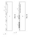
- FIG. 1Ashows a cross-sectional view of a light emitting device 10 (referred to alternatively herein as “LED”).
- the light emitting device 10comprises a substrate 20 having a recess 30 , an interlayer dielectric layer 40 being located on the substrate 20 , and having a first hole 22 and a second hole 24 , the first hole 22 opening over the recess 30 of the substrate 20 so as to communicate with the recess 30 .
- the light emitting device 10may further comprise a third hole 26 in the interlayer dielectric layer 40 having a different size from the second hole 24 .
- the first hole 22 , second hole 24 , and third hole 26have different sizes from each other. Numerous shapes are possible for the cross sections of the holes, and numerous dimensions are possible for the different sizes of the holes.
- the first hole 22 , second hole 24 , and third hole 26may be configured in circular shapes with diameters of between 95 and 115 ⁇ m, between 70 and 90 ⁇ m, and between 45 and 65 ⁇ m, respectively. And, in one more specific example the respective dimensions may be 105 ⁇ m, 80 ⁇ m, and 55 ⁇ m.
- the effective diameter of the holesare sized to be a few microns (e.g., 1-6 ⁇ m, and more typically 3 ⁇ m) larger than the corresponding micro LEDs to allow the micro LEDs to fit within the holes without being too easily dislodged.
- the holesare configured to mechanically trap micro LEDs of different sizes during fluid transport in the manufacturing process, as explained in more detail below.
- the first hole 22is delineated on the top and bottom by dotted lines A and B, respectively, and the recess 30 is delineated on the top by dotted line B.
- Dotted line Arepresents an imaginary plane that extends over the first hole 22 along the plane of the upper surface of the interlayer dielectric layer 40
- dotted line Brepresents an imaginary plane delineating the boundary between the first recess 30 and the first hole 22 , extending over the first recess 30 along the plane of the upper surface of the substrate 20 .
- the depth of the recess 30is configured to be substantially equal to a thickness of the interlayer dielectric layer 40 , although it will be appreciated that other configurations are possible and the recess 30 may be shallower or deeper than the thickness of the interlayer dielectric layer 40 , with the total thickness of the recess 30 and first hole 22 being selected to match the thickness of a corresponding micro LED, as described below. Accordingly, a trapping site is created that can selectively trap larger devices.
- the first hole 22 , second hole 24 , and third hole 26may be configured with thicknesses that are substantially equal to the thickness of the interlayer dielectric layer 40 .
- the thickness of the interlayer dielectric layer 40may be selected to be between 0.1 and 100 ⁇ m, and more specifically may be selected to be between 1 and 50 ⁇ m, and in one particular embodiment may be 5 ⁇ m.
- FIG. 1Ait will be appreciated that the micro LEDs have been removed for illustrative purposes.
- the recess 30is provided on the upper surface of the substrate 20 , which is preferably a transparent substrate that may comprise or be formed of a plastic, polymer (polyimide, for example), or glass (perforated glass, quartz glass, or sapphire glass, for example).
- the transparent substratemay alternatively be a laminated sheet comprising a substrate having two layers.
- a depth of the recess 30is typically selected to be between 0.1 and 100 ⁇ m, and more specifically may be between 1 and 50 ⁇ m, and in one particular embodiment may be 5 ⁇ m.
- the recess 30may be configured in a shape and dimension that corresponds to the first hole 22 , which in one specific example may be a circular shape with a diameter of between 95 and 115 ⁇ m, or more specifically of 105 ⁇ m.
- the recesses 30could be embossed or etched to have different depths on the same substrate 20 to accommodate micro LED devices of different depths.
- the interlayer dielectric layer 40typically located on the upper surface of the substrate 20 , comprises a polymeric material such as an acrylic resin or a polyimide resin in this embodiment, but may also comprise a silicon nitride (SiNx) or a silicon oxide (SiO) instead.
- a thickness of the interlayer dielectric layer 40may be configured to range between 0.1 and 100 ⁇ m, and more specifically between 1 and 50 ⁇ m.
- the micro LEDsare depicted in the holes and recess 30 to illustrate the final assembly of the light emitting device 10 .
- a first micro LED 12has a thickness greater than a second micro LED 14 and is placed in the first hole 22
- the second micro LED 14is located in the second hole 24 .
- a third micro LED 16may be located in the third hole 26 and may have a different size from the second micro LED 14 .
- the first micro LED 12 and second micro LED 14may be provided on the light emitting device 10 , such that an upper surface of the interlayer dielectric layer 40 , an upper surface of the first micro LED 12 , and an upper surface of the second micro LED 14 are substantially level, obviating the need to planarize the upper surface of the light emitting device 10 following assembly by using a polishing process, such as CMP, or by adding additional layers, etc. In this manner, cover layers such as optical films, etc., may be easily manufactured on a level surface over the light emitting device 10 .
- the first hole 22 and second hole 24are respectively configured to be slightly larger than their corresponding micro LEDs, namely, first micro LED 12 and second micro LED 14 .
- the diameters of the micro LEDsare configured so that the first hole 22 , second hole 24 , and third hole 26 have diameters that area predetermined distance, such as 5 ⁇ m, larger than the first micro LED 12 , second micro LED 14 , and third micro LED 16 , respectively, allowing the micro LEDs to easily settle into their respective holes during fluidic transport assembly, as described below.
- the upper surfaces of the first micro LED 12 , second micro LED 14 , and third micro LED 16may be lower than the upper surface of the interlayer dielectric layer 40 , and a subsequent planarization process may be applied, if desired, to planarize the upper surface of the assembly, for example, by adding material on top of the micro LEDs or by removing material on the upper surface of the interlayer dielectric layer 40 .
- the first micro LED 12 , the second micro LED 14 , and the third micro LED 16also have different sizes, and these different sizes may be expressed in terms of the differences in their respective upper surface areas.
- an area of the upper surface of the first micro LED 12is larger than an area of the upper surface of the second micro LED 14 , and which in turn is larger than an area of the upper surface of the third micro LED 16 .
- the area of the upper surface of the second micro LED 14 and the corresponding upper opening of the second hole 24may be at least 1.2 times larger than the upper surface of the third micro LED 16 and the corresponding upper opening of the third hole 26 , and more specifically may be over 1.5 times larger. It will be appreciated that it is desirable to obtain uniform perceived brightness among the micro LEDs, and accordingly these exemplary differences in dimensions are based upon differences in the emissions intensities in each type of micro LED, and also account for manufacturing process margins, cost, and other factors.
- the shape of the micro LEDsin the depicted embodiment, the micro LEDs are configured in cylindrical shapes.
- the first micro LED 12may have a 100 ⁇ m diameter
- the second micro LED 14may have a 75 ⁇ m diameter
- the third micro LED 16may have a 50 ⁇ m diameter. It will be appreciated, however, that the diameters may range between 1 and 1000 ⁇ m.
- the micro LEDscan be self-assembled through fluidic transport in successive waves in which the largest type of micro LED is first transported and fills up available sites, the next largest type of micro LED is next transported and fills up available mid-sized sites, and finally the smallest type of micro LED is transported and fills the remaining sites, to achieve a planar upper surface on the light emitting device 10 with substantially all sites filled, without requiring the use of polishing methods, such as CMP, or additive leveling methods after assembly.
- polishing methodssuch as CMP, or additive leveling methods after assembly.
- the first micro LED 12 , second micro LED 14 , and third micro LED 16may be configured to emit red, green, and blue light, respectively, and together may function as a pixel that emits blended light of a desired color and intensity.
- the red micro LEDgenerally may be gallium arsenide based, and as a result may be thicker than the blue and green micro LEDs, which may be gallium nitride based.
- the red micro LEDtypically has a weaker emission intensity per unit area, so the red micro LED is may be configured to have a larger emission area to compensate and thereby achieve similar emission intensities as the other micro LEDs. In this way, the thicknesses and areas of the micro LEDs may vary.
- the thickness of the first micro LED 12may be greater than the thicknesses of the second micro LED 14 and the third micro LED 16 , respectively.
- the first micro LED 12may have a 10 ⁇ m thickness
- the second micro LED 14may have a 5 ⁇ m thickness
- the third micro LED 16may have a 5 ⁇ m thickness, although variations of these thicknesses are possible.
- This particular configuration of the thicknessesallows the upper surface of the interlayer dielectric layer 40 and the upper surfaces of the first micro LED 12 , second micro LED 14 , and third micro LED 16 to be substantially level without the need to apply a polishing process, such as a CMP process, to planarize the upper surface of the light emitting device 10 .
- the first micro LED 12 , second micro LED 14 , and third micro LED 16have upper surfaces configured as light emitting faces emitting known peak spectra, and back surfaces configured as connecting electrodes.
- the first micro LED 12may comprise aluminum gallium indium phosphide (AlGaInP) with a peak spectrum of 630 nm (red)
- the second micro LED 14may comprise indium gallium nitride (InGaN) with a peak spectrum of 517 nm (green)
- the third micro LED 13may comprise gallium nitride (GaN) with a peak spectrum of 460 nm (blue).
- LEDs of different thicknessmay be easily and surely positioned on the substrate 20 , so that a planar upper surface is achieved on the light emitting device 10 without the use of polishing methods after assembly, such as CMP, or additive leveling.
- FIG. 2shows a magnified, cross-sectional view of a light emitting device 110 in the vicinity of the first micro LED 112 .
- the recess 130 of the substrate 120may have a tapered shape, as viewed in cross section, and the first hole 122 in the interlayer dielectric layer 140 also has a tapered shape as viewed in cross section.
- T 1 and T 2are the taper angles, relative to horizontal, of the recess 130 and first hole 122 respectively.
- T 3is the taper angle, relative to horizontal, of the first micro LED 112 .
- T 3is the same as T 1 and T 2 , but it will be appreciated that T 3 may differ from T 1 and/or T 1 .
- the recess 130 and the first hole 122may be tapered at a 30 to 60 degree angle relative to a horizontal orientation, such that angles T 1 and T 2 are formed at angles between 30 and 60 degrees.
- the angles T 1 and T 2may be formed at 45 degrees, as depicted. While T 1 and T 2 are illustrated as being the same value in the depicted embodiment, it will be appreciated that each of T 1 and T 2 may be a different angle that is formed within the range of 30 to 60 degrees, for example.
- the tapered structureshelp orient electrodes and micro LEDs to align properly as the micro LEDs are fluidically transported over the holes, and settle into the holes under the influence of gravity.
- the shape of the first micro LED 112may be a disc shape or a polygonal shape such as an octagon or hexagon, and have tapered sides that are configured similarly to the tapered recess and hole described above. Due to the tapered sides, an area of the lighting surface 112 a (i.e., upper surface) is larger than an area of an electrode surface 112 b (i.e., bottom surface) of the first micro LED 112 .
- the first micro LED 112located in the first hole 122 and recess 130 , is configured in a shape that allows it to fit easily into the first hole 122 and the recess 130 .
- a second micro LED and a third micro LED, and their corresponding holes, described below,may have a similar structure as the first micro LED 112 .
- the disc-shape or polygon-shape described aboveaids in inhibiting the micro LEDs from aggregating together as a mass during fluid transport of the micro LEDs during the manufacturing process, thereby promoting their distribution across an entire substrate and quick settling into the holes distributed across the substrate.
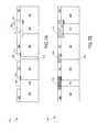
- a top plan view of a dot-pattern area 244 of a light emitting device 210 of the third embodimentis illustrated, which may also be referred to as a pixel.
- the light emitting device 210may comprise a plurality of such dot patterns as embodied by the dot-pattern area 244 , for example arranged in rows and columns as a grid or other repeating pattern as a display, television, ceiling light, car light, etc.
- the light emitting device 210 of this embodimenthas four micro LEDs configured within the dot-pattern area 244 , comprising the first micro LED 212 which is configured to emit red light, the second micro LED 214 which is configured to emit green light, the third micro LED 216 which is configured to emit blue light, and a fourth micro LED 218 which is also configured to emit blue light.
- the configuration of two blue micro LEDs in the dot-pattern area 244is intended to improve the color gamut by accounting for the fact that spectral sensitivity in humans is generally weaker at shorter wavelengths (in humans, spectral sensitivity is identified at three peaks roughly corresponding to red, green, and blue, respectively; the strongest peak is green, followed by red and blue).
- the third micro LED 216 and fourth micro LED 218may not necessary have the same peak spectrum.
- the third micro LED 216may comprise GaN with a peak spectrum of 450 nm
- the fourth micro LED 218may comprise GaN with a peak spectrum of 470 nm.
- the four micro LEDs depicted in FIG. 3Aare configured in cylindrical shapes, although other shapes may be used.
- the first micro LED 212may have a diameter between 90 and 110 ⁇ m, such as 100 ⁇ m
- the second micro LED 214may have a diameter between 65 and 85 ⁇ m, such as 75 ⁇ m
- the third and fourth micro LEDs 216 , 218may have a diameter between 40 and 60, such as 50 ⁇ m, for example.
- the red micro LEDis often configured to be thicker than the green or blue micro LEDs due to its constituent materials.
- the thickness of the first micro LED 212is typically configured to be thicker than the second, third, and fourth micro LEDs 214 , 216 , 218 .
- the first micro LED 212may have a thickness between 8 and 12 ⁇ m, such as 10 ⁇ m
- the second micro LED 214may have a thickness between 4 and 6 ⁇ m, such as 5 ⁇ m
- the third and fourth micro LEDs 216 , 218may have a thickness between 4 and 6 ⁇ m, such as 5 ⁇ m.
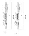
- FIG. 3Ba top plan view of the electrodes 242 a , 242 b , and 242 c in the dot-pattern area 244 of the light emitting device 210 is illustrated.
- the micro LEDshave been removed in this drawing for illustrative purposes.
- the first hole 222 , second hole 224 , third hole 226 , and fourth hole 228are located in the interlayer dielectric layer 240 .
- the first electrode 242 ais configured to electrically contact an electrode surface of the first micro LED 212 placed in the first hole 222
- the second electrode 242 bis configured to electrically contact an electrode surface of the second micro LED 214 placed in the second hole 224
- the third electrode 242 cis configured to electrically contact electrode surfaces of both the third micro LED 216 placed in the third hole 226 and fourth micro LED 218 placed in the fourth hole 228 .
- the first electrode 242 a , second electrode 242 b , and third electrode 242 cdo not intersect each other.
- the third electrode 14 cis shaped in a zigzag pattern to avoid contact with the first micro LED 212 or the second micro LED 214 and their respective electrodes.
- the interlayer dielectric layer 240not only isolates the electrodes 242 a , 242 b , and 242 c for the micro LEDs, but also provides holes that serve to selectively trap disposed devices while excluding larger devices. Solder or eutectic contact may be relied upon to ensure good electrical contact between the electrodes and the disposed devices. Solder may also be liquid during assembly and provide capillary force interaction with devices to aid in trapping.
- a top plan view of a dot-pattern area 444 (i.e., a pixel) of a light emitting device 410 of the fifth embodimentis illustrated, in which the sizes of each of the holes formed therein for the associated micro LEDs have been adjusted as compared to the embodiment of FIGS. 3A and 3B to account for human spectral sensitivity.
- the light emitting device 410may comprise a plurality of such dot patterns as embodied by the dot pattern area 444 .
- the micro LEDshave been removed in this drawing for illustrative purposes.
- the first holes 422 a - b , second holes 424 a - c , and third holes 426 a - dare located in the interlayer dielectric layer 440 .
- the first top lead electrode 442 d and first bottom lead electrode 442 aare configured to electrically contact electrode surfaces of the red micro LEDs that are placed in the first holes 422 a - b , thereby forming the red sub-pixel.
- the second top lead electrode 442 e and second bottom lead electrode 442 bare configured to electrically contact electrode surfaces of the green micro LEDs that are placed in the second holes 424 a - c , thereby forming the green sub-pixel.
- the third top lead electrode 442 f and third bottom lead electrode is 442 aare configured to electrically contact electrode surfaces of the blue micro LEDs that are placed in the third holes 426 a - d , thereby forming the blue sub-pixel.
- the top lead electrodes 442 d - f and bottom lead electrodes 442 a - cdo not form electrical connections where they intersect each other, but electrically contact the micro LEDs. It will be appreciated that each micro LED is configured with two electrical leads: one to electrically connect with a top lead electrode and another to electrically connect with a bottom lead electrode.
- the first micro LED splaced in the first holes 422 a - bmay have a diameter between 20 and 75 ⁇ m, such as 45 ⁇ m
- the second micro LED splaced in the second holes 424 a - cmay have a diameter between 40 and 100 ⁇ m, such as 70 ⁇ m
- the third micro LEDs placed in the third holes 426 a - dmay have a diameter between 50 and 200 ⁇ m, such as 100 ⁇ m, for example.
- the largest diameter micro LEDsare transported a first stage to fill the largest diameter holes, followed by the second largest in a second stage, and then followed by the third largest in a third stage.
- the total micro LED area for all LEDs in the blue, red, and green sub-pixelsmay be set to have ratio of 6:3:2 (for blue:red:green).
- the depths for the holes 422 a - b containing the red micro LEDsare typically deeper than the holes 424 a - c , 426 a - d for the blue and green micro LEDs, to accommodate thicker red micro LEDs, and thus of these holes only holes 422 a - b have a cross sectional structure including a recess extending into the substrate, similar to recess 30 in the embodiment of FIG. 1A , discussed above.
- the red micro LEDs that are inserted into this embodimentare manufactured with aluminum gallium indium phosphide (AlGaInP) while the blue and green LEDs are based on gallium nitride (GaN) with different amounts of indium doping.
- AlGaInPaluminum gallium indium phosphide
- GaNgallium nitride
- the thicknesses of the blue and green micro LEDsare the same at about 5 ⁇ m, while the red micro LEDs are around 10 ⁇ m thick or greater.
- the size, location, and number of the micro LEDs in this embodimenthave been adjusted to achieve the same or similar luminance for each color of sub-pixel, accounting for the variance in luminous intensity per unit area of the LEDs themselves and variance in human vision sensitivity to the wavelengths of red, blue and green light emitted by each sub-pixel.
- FIGS. 4A-Fare views in cross section illustrating manufacturing steps of an example method for producing the light emitting device 10 of FIGS. 1A-B , in accordance with the first embodiment of the present invention.
- FIGS. 4A-Bshow the situation when the substrate 20 is formed over a base (for the sake of brevity, the base is omitted in the Figures).
- a resist layer 46is deposited over the substrate 20 as a mask layer, patterned to predetermined patterns by photolithography, and etched by wet etching or embossed to form a recess 30 on the substrate 20 .
- the depth of the recess 30 formed in the substrate 20is configured to be substantially equal to a thickness (i.e., depth) of the first hole 22 in the interlayer dielectric layer 40 . Accordingly, a trapping site that can selectively trap larger devices is created.
- the resist layer 46is subsequently removed by ashing or dissolution.
- FIG. 4Cshows the situation when electrodes 42 are formed on the substrate 20 with a recess 30 .
- the electrodes 14may comprise a metal, such as aluminum, copper, or ITO (Indium Tin Oxide).
- the electrodes 14can be formed by sputtering, plating, and lift-off methods, for example.
- the electrodes 14make electrical connections with the electrode surfaces of the micro LEDs that are correctly disposed and aligned inside their respective holes. It will be appreciated that the electrodes 14 are configured to be thin relative to the micro LEDs, so that the thickness of the electrodes 14 does not interfere with the disposition and alignment of the micro LEDs inside their respective holes.
- the electrodes 14may be formed within dedicated recesses that are provided in the substrate 20 .
- FIG. 4Dshows the situation when the interlayer dielectric layer 40 is provided over the substrate 20 .
- a first hole 22is created in the interlayer dielectric layer 40 , opening over the recess 30 of the substrate 20 , exposing at least a part of the electrode 14 .
- a second hole 24 and third hole 26are created in the interlayer dielectric layer 40 at predetermined positions, exposing at least a part of the electrodes 14 .
- the interlayer dielectric layer 40may comprise photosensitive resin, which may be separately deposited onto the substrate 20 or manufactured from a portion of the substrate 20 through a treatment process.
- FIGS. 4E-Fdepict the first fluid transport stage. It will be appreciated that larger, heavier devices are generally fluidically transported in the first fluid transport stage, while smaller, lighter devices are fluidically transported in subsequent stages with larger devices filling larger trapping sites first and passing over smaller empty trapping sites, and smaller devices subsequently filling smaller trapping sites.
- the first micro LED 12is fluidically transported to the first hole 22 .
- the left side of the drawingrepresents the upstream portion of the fluid flow path, represented by the dark arrows, along which the micro LEDs are fluidically transported, while the right side of the drawing represents the downstream portion.
- the upstream portion and the downstream portionmay be designated at other sites on the light emitting device 10 relative to the holes and the substrate 20 .
- the first micro LED 12is transferred into a fluid to form an ink or slurry.
- the slurryis then dispensed over the upper surface of the substrate 20 and the interlayer dielectric layer 40 at the upstream portion.
- the flow speed of the first fluid transport stagemay be a sustained speed of 5 to 200 ⁇ m/sec locally at the surface during a low velocity trapping period of the first fluid transport stage, where the first micro LED 12 is disposed into the first hole 22 by gravity-driven fluid transport in a downstream direction (see FIG. 4F ).
- the flowmay also oscillate or pulse at high amplitudes (e.g., greater than 1 mm/sec) during a distribution period of the first fluid transport stage in which the LEDs are distributed across the surface, provided there is also the low-velocity trapping period during which the LEDs are allowed to settle.
- high flow-entrained disc speedse.g., disc speeds that exceed approximately 200 ⁇ m/s
- the first micro LED 12may fail to self-align into the first hole 22 and recess 30 , or other components (the second micro LED 14 or the third micro LED 16 , for example) may be disposed into the first hole 22 instead of the first micro LED 12 . It will be appreciated that the disc speed at which self-alignment may fail to occur is influenced by the disc and well size.
- the relationship between the disc speed and fluid flow speedis influenced by the properties of the transport fluid. Accordingly, disc speeds ranging from 5 to 100 ⁇ m/s locally at the surface improve the alignment and disposition of the first micro LED 12 in the first hole 22 . It will be appreciated that the first fluid transport stage may be repeated multiple times in one manufacturing process at variable flow speeds and directions.
- FIGS. 4G-Hdepict the second and third fluid transport stages, respectively.
- the second micro LED 14is fluidically transported to the second hole 24 .
- the third micro LED 16is fluidically transported to the third hole 26 .
- the left side of the drawingrepresents the upstream portion of the fluid flow path, represented by the dark arrows, along which the micro LEDs are fluidically transported, while the right side of the drawing represents the downstream portion.
- the upstream portion and the downstream portionmay be designated at other sites on the light emitting device 10 relative to the holes and the substrate 20 .
- the second micro LED 14is initially transferred into a fluid to form an ink or slurry.
- the third micro LED 16is initially transferred into a fluid to form an ink or slurry.
- the slurryis then dispensed over the upper surface of the substrate 20 and the interlayer dielectric layer 40 at the upstream portion.
- the second and third fluid transport stagesmay be repeated multiple times in one manufacturing process at variable flow speeds and directions.
- the flow speed of the second fluid transport stagemay be a sustained speed of 5 to 100 ⁇ m/s during a trapping period of the second fluid transport stage, where the second micro LED 14 is disposed into the second hole 24 by fluid transport in a downstream direction, and components other than the second micro LED 14 are dislodged from the second hole 24 .
- Higher speedssuch as 1 mm/s may be used during a distribution period of the second fluid transport stage, to distribute the LEDs of that stage across the surface for settling.
- FIG. 5Adepicts a situation where fluid transport dislodges the third micro LED 16 from the second hole 24 .
- the second micro LED 14may fail to self-align into the second hole 24 , or other components may be disposed into the second hole 24 instead of the second micro LED 14 .
- FIG. 5Bdepicts a situation where the third micro LED 16 is disposed in the second hole 24 instead of the second micro LED 14 . Accordingly, sustained flow speeds ranging from 5 to 100 ⁇ m/s improve the alignment and disposition of the second micro LED 14 in the second hole 24 , while worsening the alignment and disposition of other components in the second hole 24 , especially when the slurry includes various components that are dispensed in the same transport stage.
- the third micro LED 16is transported at a flow speed within a range (5 to 100 ⁇ m/s sustained, for example) that allows it to self-align into the third hole 26 .
- the flow speed of the first fluid transport stagemay be configured to be faster than the flow speeds of the second and third fluid transport stages. Accordingly, the fluidic self-assembly of the first micro LED 12 is possible despite its heavier mass relative to the second micro LED 14 and third micro LED 16 . It will be appreciated that other processes may be simultaneously utilized during the fluid transport stages to affect the fluid transport of the micro LEDs, such as various scattering techniques to help evenly distribute the micro LEDs during fluid transport. Following assembly, the ink or slurry is subsequently removed from the light emitting device 10 through a process such as evaporation.
- FIG. 6is a view in cross section illustrating manufacturing steps of a modified example method for producing the light emitting device 10 of FIGS. 1A-B , in accordance with the first embodiment of the present invention.
- the left side of the drawingrepresents the upstream portion of the fluid flow path, represented by the dark arrows, along which the micro LEDs are fluidically transported, while the right side of the drawing represents the downstream portion.
- the upstream portion and the downstream portionmay be designated at other sites on the light emitting device 10 relative to the holes and the substrate 20 .
- FIG. 6shows a modified second fluid transport stage in which the second micro LED 14 is fluidically transported to the second hole 24 , and the third micro LED 16 is fluidically transported to the third hole 26 .
- the modified second fluid transport stagecombines the second fluid transport stage and the third fluid transport stage, as depicted in FIGS. 4G-H , into one stage.
- the second micro LED 14 and the third micro LED 16are initially transferred into a fluid to form an ink or slurry.
- the slurryis then dispensed over the upper surface of the substrate 20 and the interlayer dielectric layer 40 at the upstream portion.
- the flow speeds of the modified second fluid transport stagemay be configured within a range that allows the second micro LED 14 and the third micro LED 16 to properly self-align into the second hole 24 and the third hole 26 , respectively.
- FIG. 7Ashows a cross-section view of a light emitting device 310 .
- the substrate 320 of this embodimenthas a first through hole 332 formed at a bottom of the recess 330 and opening to communicate with the corresponding first hole 322 opening over the recess 330 of the substrate 320 .
- the substrate 320also has a second through hole 334 , formed at a bottom of the second hole 324 in the interlayer dielectric layer 340 , which is not positioned over the recess 330 .
- a third through hole 336is also provided on the substrate 320 , formed at a bottom of the third hole 326 in the interlayer dielectric layer 340 .
- the method described above for manufacturing a light emitting devicemay be modified, so as to manufacture the light emitting device 310 , by further comprising forming a plurality of through holes (first through hole 332 , second through hole 334 , and third through hole 336 ), each of the through holes corresponding to one of the first hole 322 and second hole 324 of the interlayer dielectric layer 340 .
- the first through hole 332is configured to have a larger width than the second through hole 334 , which in turn has a larger width than the third through hole 336 .
- the first through hole 332 , second through hole 334 , and third through hole 336are formed in the substrate 320 by etching.
- the first through hole 332formed at a bottom of the recess 330 , is predetermined at the first hole 322 in the interlayer dielectric layer 340 .
- the second through hole 334 and third through hole 336are formed in the substrate 320 , which are predetermined in the interlayer dielectric layer 340 at the bottom of the second hole 324 and third hole 326 , respectively.
- the first through hole 332 , second through hole 334 , and third through hole 336are configured to draw a portion of the transport fluid in the first fluid transport stage or the second fluid transport stage.
- a vacuum apparatus(not shown) draws a portion of transport fluid through the first through hole 332 to draw the first micro LED 312 into the first hole 322 and the recess 330 by fluid transport.
- the vacuum apparatusalso draws particles through the second through hole 334 and the third through hole 336 .
- the micro LEDsare very small and thin and sometimes break during or prior to the manufacturing process. Thus, broken pieces of the first micro LEDs can form the particles that pass through the through hole 332 .
- a vacuum apparatusdraws a portion of transport fluid through the second through hole 334 and third through hole 336 to draw the second micro LED 314 and third micro LED 316 into the second hole 324 and third hole 326 , respectively, by fluid transport.
- the vacuum apparatusalso draws particles through the first through hole 332 .
- the particlesmay include broken pieces of the second micro LEDs 314 and the third micro LEDs 316 .
- the ink or slurryis subsequently removed from the light emitting device 310 through a process such as evaporation.
- the inclusion of through holes at each assembly sitecould remove debris, such as ink impurities or device fragments.
- the through holes combined with the holes and recessesmay enable the simultaneous and selective self-assembly of micro LEDs, potentially simplifying and shortening the assembly process, as well as enabling the reuse of captured, undisposed devices.
Landscapes
- Engineering & Computer Science (AREA)
- Microelectronics & Electronic Packaging (AREA)
- Power Engineering (AREA)
- Computer Hardware Design (AREA)
- Physics & Mathematics (AREA)
- Condensed Matter Physics & Semiconductors (AREA)
- General Physics & Mathematics (AREA)
- Manufacturing & Machinery (AREA)
- Led Device Packages (AREA)
- Led Devices (AREA)
- Devices For Indicating Variable Information By Combining Individual Elements (AREA)
Abstract
Description
- This application is a continuation of U.S. patent application Ser. No. 15/650,192 entitled “LIGHT EMITTING DEVICE AND FLUIDIC MANUFACTURE THEREOF”, and filed by Sasaki et al. on Jul. 14, 2017, which in turn is a continuation of U.S. Pat. No. 9,722,145 entitled “LIGHT EMITTING DEVICE AND FLUIDIC MANUFACTURE THEREOF”, and filed by Sasaki et al. on Jun. 24, 2015.
- Light emitting devices (LEDs) are anticipated to be used in future high-efficiency lighting applications, such as displays and lights. Recently, micro LEDs have been developed for future high-efficiency lighting applications. One challenge associated with such devices is that the assembly of micro-scale components can be costly and complicated, making it difficult to achieve high assembly accuracy at a reasonable manufacturing cost.
- Methods for the distribution or alignment of small devices onto a transparent substrate, such as glass or a polymer, to create light emitting devices are well known in the art. One cost-effective method is fluidic self-assembly, in which a liquid carrier medium of an ink or slurry is filled with small lighting devices, and allowed to flow over the substrate. The small lighting devices are carried across the substrate by fluid transport, and gravity is used to mechanically trap the small lighting devices in mechanical trapping sites on the substrate in the manufacturing process. However, in conventional fluidic self-assembly methods, when small devices with different sizes are trapped in trapping sites, the devices are often misaligned or disposed in the incorrect sites. Moreover, even when the devices are correctly aligned and disposed in the correct sites, the resulting surface of the light emitting device may not be planar, requiring a polishing step after assembly, which compromises the cost-effectiveness of the manufacturing process, and in some cases can undesirably alter the precise positioning of the small lighting devices.
- To address the above issues, light emitting devices and methods for their manufacture are provided. According to one aspect, alight emitting device is provided that comprises a substrate having a recess, and an interlayer dielectric layer located on the substrate. The interlayer dielectric layer may have a first hole and a second hole, the first hole opening over the recess of the substrate. The light emitting device may further include a first and second micro light emitting device, the first micro light emitting device having a thickness greater than a second micro light emitting device. The first micro light emitting device and the second micro light emitting device may be placed in the first hole and the second hole, respectively.
- This Summary is provided to introduce a selection of concepts in a simplified form that are further described below in the Detailed Description. This Summary is not intended to identify key features or essential features of the claimed subject matter, nor is it intended to be used to limit the scope of the claimed subject matter. Furthermore, the claimed subject matter is not limited to implementations that solve any or all disadvantages noted in any part of this disclosure.
- The present disclosure is illustrated by way of example and not by way of limitation in the figures of the accompanying drawings, in which the like reference numerals indicate like elements.
FIGS. 1A-B show schematic diagrams of a light emitting device according to a first embodiment of the present invention.FIG. 2 shows a schematic diagram of a light emitting device according to a second embodiment of the present invention.FIGS. 3A-B show schematic diagrams of a light emitting device according to a third embodiment of the present invention.FIGS. 3C shows a schematic diagram of a light emitting device according to a fifth embodiment of the present invention.FIGS. 4A-H show an overview of the process for producing a light emitting device in accordance with the first embodiment of the present invention.FIGS. 5A-B show schematic diagrams of a self-alignment process for producing a light emitting device in accordance with the first embodiment of the present invention.FIG. 6 shows an overview of a modified process for producing a light emitting device in accordance with the first embodiment of the present invention.FIGS. 7A-B show schematic diagrams of a light emitting device according to a fourth embodiment of the present invention.- Selected embodiments of the present invention will now be described with reference to the accompanying drawings. It will be apparent to those skilled in the art from this disclosure that the following descriptions of the embodiments of the invention are provided for illustration only and not for the purpose of limiting the invention as defined by the appended claims and their equivalents.
- Referring initially to
FIG. 1A , alight emitting device 10 is provided according to the first embodiment of the present invention.FIG. 1A shows a cross-sectional view of a light emitting device10 (referred to alternatively herein as “LED”). Thelight emitting device 10 comprises asubstrate 20 having arecess 30, an interlayerdielectric layer 40 being located on thesubstrate 20, and having afirst hole 22 and asecond hole 24, thefirst hole 22 opening over therecess 30 of thesubstrate 20 so as to communicate with therecess 30. Thelight emitting device 10 may further comprise athird hole 26 in the interlayerdielectric layer 40 having a different size from thesecond hole 24. Typically, thefirst hole 22,second hole 24, andthird hole 26 have different sizes from each other. Numerous shapes are possible for the cross sections of the holes, and numerous dimensions are possible for the different sizes of the holes. In one specific example, thefirst hole 22,second hole 24, andthird hole 26 may be configured in circular shapes with diameters of between 95 and 115 μm, between 70 and 90 μm, and between 45 and 65 μm, respectively. And, in one more specific example the respective dimensions may be 105 μm, 80 μm, and 55 μm. Typically, the effective diameter of the holes are sized to be a few microns (e.g., 1-6 μm, and more typically 3 μm) larger than the corresponding micro LEDs to allow the micro LEDs to fit within the holes without being too easily dislodged. With this configuration, the holes are configured to mechanically trap micro LEDs of different sizes during fluid transport in the manufacturing process, as explained in more detail below. - In
FIG. 1A , thefirst hole 22 is delineated on the top and bottom by dotted lines A and B, respectively, and therecess 30 is delineated on the top by dotted line B. Dotted line A represents an imaginary plane that extends over thefirst hole 22 along the plane of the upper surface of the interlayerdielectric layer 40, while dotted line B represents an imaginary plane delineating the boundary between thefirst recess 30 and thefirst hole 22, extending over thefirst recess 30 along the plane of the upper surface of thesubstrate 20. In the depicted embodiment, the depth of therecess 30 is configured to be substantially equal to a thickness of the interlayerdielectric layer 40, although it will be appreciated that other configurations are possible and therecess 30 may be shallower or deeper than the thickness of the interlayerdielectric layer 40, with the total thickness of therecess 30 andfirst hole 22 being selected to match the thickness of a corresponding micro LED, as described below. Accordingly, a trapping site is created that can selectively trap larger devices. Thefirst hole 22,second hole 24, andthird hole 26 may be configured with thicknesses that are substantially equal to the thickness of the interlayerdielectric layer 40. In an example configuration, the thickness of the interlayerdielectric layer 40 may be selected to be between 0.1 and 100 μm, and more specifically may be selected to be between 1 and 50 μm, and in one particular embodiment may be 5 μm. InFIG. 1A , it will be appreciated that the micro LEDs have been removed for illustrative purposes. - The
recess 30 is provided on the upper surface of thesubstrate 20, which is preferably a transparent substrate that may comprise or be formed of a plastic, polymer (polyimide, for example), or glass (perforated glass, quartz glass, or sapphire glass, for example). The transparent substrate may alternatively be a laminated sheet comprising a substrate having two layers. A depth of therecess 30 is typically selected to be between 0.1 and 100 μm, and more specifically may be between 1 and 50 μm, and in one particular embodiment may be 5 μm. Therecess 30 may be configured in a shape and dimension that corresponds to thefirst hole 22, which in one specific example may be a circular shape with a diameter of between 95 and 115 μm, or more specifically of 105 μm. Alternatively, therecesses 30 could be embossed or etched to have different depths on thesame substrate 20 to accommodate micro LED devices of different depths. - The
interlayer dielectric layer 40, typically located on the upper surface of thesubstrate 20, comprises a polymeric material such as an acrylic resin or a polyimide resin in this embodiment, but may also comprise a silicon nitride (SiNx) or a silicon oxide (SiO) instead. A thickness of theinterlayer dielectric layer 40 may be configured to range between 0.1 and 100 μm, and more specifically between 1 and 50 μm. - Referring to
FIG. 1B , the micro LEDs are depicted in the holes andrecess 30 to illustrate the final assembly of thelight emitting device 10. A firstmicro LED 12 has a thickness greater than a secondmicro LED 14 and is placed in thefirst hole 22, and the secondmicro LED 14 is located in thesecond hole 24. A thirdmicro LED 16 may be located in thethird hole 26 and may have a different size from the secondmicro LED 14. The firstmicro LED 12 and secondmicro LED 14 may be provided on thelight emitting device 10, such that an upper surface of theinterlayer dielectric layer 40, an upper surface of the firstmicro LED 12, and an upper surface of the secondmicro LED 14 are substantially level, obviating the need to planarize the upper surface of thelight emitting device 10 following assembly by using a polishing process, such as CMP, or by adding additional layers, etc. In this manner, cover layers such as optical films, etc., may be easily manufactured on a level surface over thelight emitting device 10. Thefirst hole 22 andsecond hole 24 are respectively configured to be slightly larger than their corresponding micro LEDs, namely, firstmicro LED 12 and secondmicro LED 14. For example, the diameters of the micro LEDs are configured so that thefirst hole 22,second hole 24, andthird hole 26 have diameters that area predetermined distance, such as 5 μm, larger than the firstmicro LED 12, secondmicro LED 14, and thirdmicro LED 16, respectively, allowing the micro LEDs to easily settle into their respective holes during fluidic transport assembly, as described below. Alternatively, in another embodiment, the upper surfaces of the firstmicro LED 12, secondmicro LED 14, and thirdmicro LED 16 may be lower than the upper surface of theinterlayer dielectric layer 40, and a subsequent planarization process may be applied, if desired, to planarize the upper surface of the assembly, for example, by adding material on top of the micro LEDs or by removing material on the upper surface of theinterlayer dielectric layer 40. - Like the
holes micro LED 12, the secondmicro LED 14, and the thirdmicro LED 16 also have different sizes, and these different sizes may be expressed in terms of the differences in their respective upper surface areas. For example, an area of the upper surface of the firstmicro LED 12 is larger than an area of the upper surface of the secondmicro LED 14, and which in turn is larger than an area of the upper surface of the thirdmicro LED 16. As an example of the degree to which the upper surfaces areas may vary, the area of the upper surface of the secondmicro LED 14 and the corresponding upper opening of thesecond hole 24 may be at least 1.2 times larger than the upper surface of the thirdmicro LED 16 and the corresponding upper opening of thethird hole 26, and more specifically may be over 1.5 times larger. It will be appreciated that it is desirable to obtain uniform perceived brightness among the micro LEDs, and accordingly these exemplary differences in dimensions are based upon differences in the emissions intensities in each type of micro LED, and also account for manufacturing process margins, cost, and other factors. Regarding the shape of the micro LEDs, in the depicted embodiment, the micro LEDs are configured in cylindrical shapes. In one particular arrangement, the firstmicro LED 12 may have a 100 μm diameter, the secondmicro LED 14 may have a 75 μm diameter, and the thirdmicro LED 16 may have a 50 μm diameter. It will be appreciated, however, that the diameters may range between 1 and 1000 μm. It will be appreciated that due to the size differences described above, the micro LEDs can be self-assembled through fluidic transport in successive waves in which the largest type of micro LED is first transported and fills up available sites, the next largest type of micro LED is next transported and fills up available mid-sized sites, and finally the smallest type of micro LED is transported and fills the remaining sites, to achieve a planar upper surface on thelight emitting device 10 with substantially all sites filled, without requiring the use of polishing methods, such as CMP, or additive leveling methods after assembly. - The first
micro LED 12, secondmicro LED 14, and thirdmicro LED 16 may be configured to emit red, green, and blue light, respectively, and together may function as a pixel that emits blended light of a desired color and intensity. The red micro LED generally may be gallium arsenide based, and as a result may be thicker than the blue and green micro LEDs, which may be gallium nitride based. The red micro LED typically has a weaker emission intensity per unit area, so the red micro LED is may be configured to have a larger emission area to compensate and thereby achieve similar emission intensities as the other micro LEDs. In this way, the thicknesses and areas of the micro LEDs may vary. As example thicknesses, the thickness of the firstmicro LED 12 may be greater than the thicknesses of the secondmicro LED 14 and the thirdmicro LED 16, respectively. In one particular embodiment, the firstmicro LED 12 may have a 10 μm thickness, the secondmicro LED 14 may have a 5 μm thickness, and the thirdmicro LED 16 may have a 5 μm thickness, although variations of these thicknesses are possible. This particular configuration of the thicknesses allows the upper surface of theinterlayer dielectric layer 40 and the upper surfaces of the firstmicro LED 12, secondmicro LED 14, and thirdmicro LED 16 to be substantially level without the need to apply a polishing process, such as a CMP process, to planarize the upper surface of thelight emitting device 10. - The first
micro LED 12, secondmicro LED 14, and thirdmicro LED 16 have upper surfaces configured as light emitting faces emitting known peak spectra, and back surfaces configured as connecting electrodes. For example, the firstmicro LED 12 may comprise aluminum gallium indium phosphide (AlGaInP) with a peak spectrum of 630 nm (red), the secondmicro LED 14 may comprise indium gallium nitride (InGaN) with a peak spectrum of 517 nm (green), and the third micro LED13 may comprise gallium nitride (GaN) with a peak spectrum of 460 nm (blue). - By providing such a
light emitting device 10 as shown in the first embodiment, which includes therecess 30 of thesubstrate 20, and theinterlayer dielectric layer 40 having afirst hole 22 and asecond hole 24, thefirst hole 22 opening over therecess 30 of thesubstrate 20, a firstmicro LED 12 having a thickness greater than a secondmicro LED 14, and the firstmicro LED 12 and the secondmicro LED 14 being placed in thefirst hole 22 and thesecond hole 24, respectively, LEDs of different thickness may be easily and surely positioned on thesubstrate 20, so that a planar upper surface is achieved on thelight emitting device 10 without the use of polishing methods after assembly, such as CMP, or additive leveling. - Referring to
FIG. 2 , alight emitting device 110 is provided according to the second embodiment of the present invention.FIG. 2 shows a magnified, cross-sectional view of alight emitting device 110 in the vicinity of the firstmicro LED 112. In thelight emitting device 110 of the second embodiment, therecess 130 of thesubstrate 120 may have a tapered shape, as viewed in cross section, and thefirst hole 122 in theinterlayer dielectric layer 140 also has a tapered shape as viewed in cross section. InFIGS. 2 , T1 and T2 are the taper angles, relative to horizontal, of therecess 130 andfirst hole 122 respectively. T3 is the taper angle, relative to horizontal, of the firstmicro LED 112. In the depicted embodiment, T3 is the same as T1 and T2, but it will be appreciated that T3 may differ from T1 and/or T1. For example, therecess 130 and thefirst hole 122 may be tapered at a 30 to 60 degree angle relative to a horizontal orientation, such that angles T1 and T2 are formed at angles between 30 and 60 degrees. In a more specific embodiment, the angles T1 and T2 may be formed at 45 degrees, as depicted. While T1 and T2 are illustrated as being the same value in the depicted embodiment, it will be appreciated that each of T1 and T2 may be a different angle that is formed within the range of 30 to 60 degrees, for example. In one specific alternative embodiment, thefirst hole 122 in theinterlayer dielectric layer 140 has no taper (T2=90 degrees) while the recess is tapered such that T1 is between 70 and 85 degrees, and the firstmicro LED 112 has a taper of between 70 and 85 degrees such that T1=T3. The tapered structures help orient electrodes and micro LEDs to align properly as the micro LEDs are fluidically transported over the holes, and settle into the holes under the influence of gravity. - Although only illustrated as a cross section in
FIG. 2 , it will be appreciated that the shape of the firstmicro LED 112 may be a disc shape or a polygonal shape such as an octagon or hexagon, and have tapered sides that are configured similarly to the tapered recess and hole described above. Due to the tapered sides, an area of thelighting surface 112a(i.e., upper surface) is larger than an area of anelectrode surface 112b(i.e., bottom surface) of the firstmicro LED 112. Thus, the firstmicro LED 112, located in thefirst hole 122 andrecess 130, is configured in a shape that allows it to fit easily into thefirst hole 122 and therecess 130. While only a singletapered hole 122 and single taperedmicro LED 112 are shown in thelight emitting device 110 ofFIG. 2 , it will be appreciated that this is for illustrative purposes to describe the possibility of tapered sides, and that all or a selected plurality of the holes, recesses, and micro LEDs in the other embodiments described herein may be formed with a taper similar to that shown inFIG. 2 to encompass various permutations, including an embodiment where only the holes are tapered and the micro LEDs are not tapered. Thus, a second micro LED and a third micro LED, and their corresponding holes, described below, may have a similar structure as the firstmicro LED 112. The disc-shape or polygon-shape described above aids in inhibiting the micro LEDs from aggregating together as a mass during fluid transport of the micro LEDs during the manufacturing process, thereby promoting their distribution across an entire substrate and quick settling into the holes distributed across the substrate. - Referring to
FIG. 3A , a top plan view of a dot-pattern area 244 of alight emitting device 210 of the third embodiment is illustrated, which may also be referred to as a pixel. It will be appreciated that thelight emitting device 210 may comprise a plurality of such dot patterns as embodied by the dot-pattern area 244, for example arranged in rows and columns as a grid or other repeating pattern as a display, television, ceiling light, car light, etc. Thelight emitting device 210 of this embodiment has four micro LEDs configured within the dot-pattern area 244, comprising the firstmicro LED 212 which is configured to emit red light, the secondmicro LED 214 which is configured to emit green light, the thirdmicro LED 216 which is configured to emit blue light, and a fourthmicro LED 218 which is also configured to emit blue light. The configuration of two blue micro LEDs in the dot-pattern area 244 is intended to improve the color gamut by accounting for the fact that spectral sensitivity in humans is generally weaker at shorter wavelengths (in humans, spectral sensitivity is identified at three peaks roughly corresponding to red, green, and blue, respectively; the strongest peak is green, followed by red and blue).The thirdmicro LED 216 and fourthmicro LED 218 may not necessary have the same peak spectrum. For example, the thirdmicro LED 216 may comprise GaN with a peak spectrum of 450 nm, and the fourthmicro LED 218 may comprise GaN with a peak spectrum of 470 nm. - Like the first embodiment, the four micro LEDs depicted in
FIG. 3A are configured in cylindrical shapes, although other shapes may be used. In one specific example, the firstmicro LED 212 may have a diameter between 90 and 110 μm, such as 100 μm, the secondmicro LED 214 may have a diameter between 65 and 85 μm, such as 75 μm, and the third and fourthmicro LEDs micro LED 212 is typically configured to be thicker than the second, third, and fourthmicro LEDs micro LED 212 may have a thickness between 8 and 12 μm, such as 10 μm, the secondmicro LED 214 may have a thickness between 4 and 6 μm, such as 5 μm, and the third and fourthmicro LEDs - Referring to
FIG. 3B , a top plan view of theelectrodes pattern area 244 of thelight emitting device 210 is illustrated. The micro LEDs have been removed in this drawing for illustrative purposes. Thefirst hole 222,second hole 224,third hole 226, andfourth hole 228 are located in theinterlayer dielectric layer 240. Thefirst electrode 242ais configured to electrically contact an electrode surface of the firstmicro LED 212 placed in thefirst hole 222, thesecond electrode 242bis configured to electrically contact an electrode surface of the secondmicro LED 214 placed in thesecond hole 224, and thethird electrode 242cis configured to electrically contact electrode surfaces of both the thirdmicro LED 216 placed in thethird hole 226 and fourthmicro LED 218 placed in thefourth hole 228. Thefirst electrode 242a,second electrode 242b, andthird electrode 242cdo not intersect each other. The third electrode14cis shaped in a zigzag pattern to avoid contact with the firstmicro LED 212 or the secondmicro LED 214 and their respective electrodes. - In this embodiment, the
interlayer dielectric layer 240 not only isolates theelectrodes - Referring to
FIG. 3C , a top plan view of a dot-pattern area444 (i.e., a pixel) of alight emitting device 410 of the fifth embodiment is illustrated, in which the sizes of each of the holes formed therein for the associated micro LEDs have been adjusted as compared to the embodiment ofFIGS. 3A and 3B to account for human spectral sensitivity. As with the third embodiment, it will be appreciated that thelight emitting device 410 may comprise a plurality of such dot patterns as embodied by thedot pattern area 444. The micro LEDs have been removed in this drawing for illustrative purposes. The first holes422a-b, second holes424a-c, and third holes426a-dare located in theinterlayer dielectric layer 440. The firsttop lead electrode 442dand firstbottom lead electrode 442aare configured to electrically contact electrode surfaces of the red micro LEDs that are placed in the first holes422a-b, thereby forming the red sub-pixel. The secondtop lead electrode 442eand secondbottom lead electrode 442bare configured to electrically contact electrode surfaces of the green micro LEDs that are placed in the second holes424a-c, thereby forming the green sub-pixel. The third toplead electrode 442fand third bottom lead electrode is442aare configured to electrically contact electrode surfaces of the blue micro LEDs that are placed in the third holes426a-d, thereby forming the blue sub-pixel. The toplead electrodes 442d-fand bottom lead electrodes442a-cdo not form electrical connections where they intersect each other, but electrically contact the micro LEDs. It will be appreciated that each micro LED is configured with two electrical leads: one to electrically connect with a top lead electrode and another to electrically connect with a bottom lead electrode. In this embodiment, the first micro LED splaced in the first holes422a-bmay have a diameter between 20 and 75 μm, such as 45 μm, the second micro LED splaced in the second holes424a-cmay have a diameter between 40 and 100 μm, such as 70 μm, and the third micro LEDs placed in the third holes426a-dmay have a diameter between 50 and 200 μm, such as 100 μm, for example. As discussed below, it will be appreciated that during fluidic assembly, the largest diameter micro LEDs are transported a first stage to fill the largest diameter holes, followed by the second largest in a second stage, and then followed by the third largest in a third stage. The total micro LED area for all LEDs in the blue, red, and green sub-pixels may be set to have ratio of 6:3:2 (for blue:red:green). The depths for the holes422a-bcontaining the red micro LEDs are typically deeper than the holes424a-c,426a-dfor the blue and green micro LEDs, to accommodate thicker red micro LEDs, and thus of these holes only holes422a-bhave a cross sectional structure including a recess extending into the substrate, similar torecess 30 in the embodiment ofFIG. 1A , discussed above. The red micro LEDs that are inserted into this embodiment are manufactured with aluminum gallium indium phosphide (AlGaInP) while the blue and green LEDs are based on gallium nitride (GaN) with different amounts of indium doping. The thicknesses of the blue and green micro LEDs are the same at about 5 μm, while the red micro LEDs are around 10 μm thick or greater. Of course, these are merely exemplary measurements, and LEDs of other dimensions may utilized. It will be appreciated that human vision on average is most sensitive to green light, followed by red light, and is least sensitive to blue light. Accordingly the size, location, and number of the micro LEDs in this embodiment have been adjusted to achieve the same or similar luminance for each color of sub-pixel, accounting for the variance in luminous intensity per unit area of the LEDs themselves and variance in human vision sensitivity to the wavelengths of red, blue and green light emitted by each sub-pixel. FIGS. 4A-F are views in cross section illustrating manufacturing steps of an example method for producing thelight emitting device 10 ofFIGS. 1A-B , in accordance with the first embodiment of the present invention.FIGS. 4A-B show the situation when thesubstrate 20 is formed over a base (for the sake of brevity, the base is omitted in the Figures). A resistlayer 46 is deposited over thesubstrate 20 as a mask layer, patterned to predetermined patterns by photolithography, and etched by wet etching or embossed to form arecess 30 on thesubstrate 20. The depth of therecess 30 formed in thesubstrate 20 is configured to be substantially equal to a thickness (i.e., depth) of thefirst hole 22 in theinterlayer dielectric layer 40. Accordingly, a trapping site that can selectively trap larger devices is created. The resistlayer 46 is subsequently removed by ashing or dissolution.FIG. 4C shows the situation whenelectrodes 42 are formed on thesubstrate 20 with arecess 30. Theelectrodes 14 may comprise a metal, such as aluminum, copper, or ITO (Indium Tin Oxide). Theelectrodes 14 can be formed by sputtering, plating, and lift-off methods, for example. Theelectrodes 14 make electrical connections with the electrode surfaces of the micro LEDs that are correctly disposed and aligned inside their respective holes. It will be appreciated that theelectrodes 14 are configured to be thin relative to the micro LEDs, so that the thickness of theelectrodes 14 does not interfere with the disposition and alignment of the micro LEDs inside their respective holes. To further improve the electrical connections of theelectrodes 14 with the electrode surfaces of the micro LEDs, theelectrodes 14 may be formed within dedicated recesses that are provided in thesubstrate 20.FIG. 4D , shows the situation when theinterlayer dielectric layer 40 is provided over thesubstrate 20. Afirst hole 22 is created in theinterlayer dielectric layer 40, opening over therecess 30 of thesubstrate 20, exposing at least a part of theelectrode 14. Asecond hole 24 andthird hole 26 are created in theinterlayer dielectric layer 40 at predetermined positions, exposing at least a part of theelectrodes 14. Theinterlayer dielectric layer 40 may comprise photosensitive resin, which may be separately deposited onto thesubstrate 20 or manufactured from a portion of thesubstrate 20 through a treatment process.FIGS. 4E-F depict the first fluid transport stage. It will be appreciated that larger, heavier devices are generally fluidically transported in the first fluid transport stage, while smaller, lighter devices are fluidically transported in subsequent stages with larger devices filling larger trapping sites first and passing over smaller empty trapping sites, and smaller devices subsequently filling smaller trapping sites. In the first fluid transport stage, the firstmicro LED 12 is fluidically transported to thefirst hole 22. The left side of the drawing represents the upstream portion of the fluid flow path, represented by the dark arrows, along which the micro LEDs are fluidically transported, while the right side of the drawing represents the downstream portion. However, it will be appreciated that the upstream portion and the downstream portion may be designated at other sites on thelight emitting device 10 relative to the holes and thesubstrate 20. First, the firstmicro LED 12 is transferred into a fluid to form an ink or slurry. The slurry is then dispensed over the upper surface of thesubstrate 20 and theinterlayer dielectric layer 40 at the upstream portion. The flow speed of the first fluid transport stage may be a sustained speed of 5 to 200 μm/sec locally at the surface during a low velocity trapping period of the first fluid transport stage, where the firstmicro LED 12 is disposed into thefirst hole 22 by gravity-driven fluid transport in a downstream direction (seeFIG. 4F ). The flow may also oscillate or pulse at high amplitudes (e.g., greater than 1 mm/sec) during a distribution period of the first fluid transport stage in which the LEDs are distributed across the surface, provided there is also the low-velocity trapping period during which the LEDs are allowed to settle. At high flow-entrained disc speeds (e.g., disc speeds that exceed approximately 200 μm/s), the firstmicro LED 12 may fail to self-align into thefirst hole 22 andrecess 30, or other components (the secondmicro LED 14 or the thirdmicro LED 16, for example) may be disposed into thefirst hole 22 instead of the firstmicro LED 12. It will be appreciated that the disc speed at which self-alignment may fail to occur is influenced by the disc and well size. Further, the relationship between the disc speed and fluid flow speed is influenced by the properties of the transport fluid. Accordingly, disc speeds ranging from 5 to 100 μm/s locally at the surface improve the alignment and disposition of the firstmicro LED 12 in thefirst hole 22. It will be appreciated that the first fluid transport stage may be repeated multiple times in one manufacturing process at variable flow speeds and directions.FIGS. 4G-H depict the second and third fluid transport stages, respectively. In the second fluid transport stage, the secondmicro LED 14 is fluidically transported to thesecond hole 24. In the third fluid transport stage, the thirdmicro LED 16 is fluidically transported to thethird hole 26. The left side of the drawing represents the upstream portion of the fluid flow path, represented by the dark arrows, along which the micro LEDs are fluidically transported, while the right side of the drawing represents the downstream portion. However, it will be appreciated that the upstream portion and the downstream portion may be designated at other sites on thelight emitting device 10 relative to the holes and thesubstrate 20. In the second fluid transport phase, the secondmicro LED 14 is initially transferred into a fluid to form an ink or slurry. Likewise, in the third fluid transport phase, the thirdmicro LED 16 is initially transferred into a fluid to form an ink or slurry. The slurry is then dispensed over the upper surface of thesubstrate 20 and theinterlayer dielectric layer 40 at the upstream portion. It will be appreciated that the second and third fluid transport stages may be repeated multiple times in one manufacturing process at variable flow speeds and directions.- The flow speed of the second fluid transport stage may be a sustained speed of 5 to 100 μm/s during a trapping period of the second fluid transport stage, where the second
micro LED 14 is disposed into thesecond hole 24 by fluid transport in a downstream direction, and components other than the secondmicro LED 14 are dislodged from thesecond hole 24. Higher speeds such as 1 mm/s may be used during a distribution period of the second fluid transport stage, to distribute the LEDs of that stage across the surface for settling. For example,FIG. 5A depicts a situation where fluid transport dislodges the thirdmicro LED 16 from thesecond hole 24. At flow-entrained disc speeds that exceed 100 μm/s, the secondmicro LED 14 may fail to self-align into thesecond hole 24, or other components may be disposed into thesecond hole 24 instead of the secondmicro LED 14. For example,FIG. 5B depicts a situation where the thirdmicro LED 16 is disposed in thesecond hole 24 instead of the secondmicro LED 14. Accordingly, sustained flow speeds ranging from 5 to 100 μm/s improve the alignment and disposition of the secondmicro LED 14 in thesecond hole 24, while worsening the alignment and disposition of other components in thesecond hole 24, especially when the slurry includes various components that are dispensed in the same transport stage. It is thought that, at certain flow speeds, sufficient turbulence is generated between the gaps within a hole in which a mismatched component is disposed so that the mismatched component is dislodged from the hole. At the same time, if a terminal portion of the mismatched component protrudes from the hole, the interruption of laminar flow along the surface of the LED could generate sufficient turbulence to exert upward force against the terminal portion of the mismatched component, thereby dislodging the component from the hole. It will be appreciated that, likewise, the thirdmicro LED 16 is transported at a flow speed within a range (5 to 100 μm/s sustained, for example) that allows it to self-align into thethird hole 26. To account for the heavier mass of the firstmicro LED 12 relative to the secondmicro LED 14 and the thirdmicro LED 16, the flow speed of the first fluid transport stage may be configured to be faster than the flow speeds of the second and third fluid transport stages. Accordingly, the fluidic self-assembly of the firstmicro LED 12 is possible despite its heavier mass relative to the secondmicro LED 14 and thirdmicro LED 16. It will be appreciated that other processes may be simultaneously utilized during the fluid transport stages to affect the fluid transport of the micro LEDs, such as various scattering techniques to help evenly distribute the micro LEDs during fluid transport. Following assembly, the ink or slurry is subsequently removed from thelight emitting device 10 through a process such as evaporation. - By the sequential batch assembly method described above, large devices can be located in larger holes while being prevented from trapping in smaller wells. Subsequently, smaller devices can then assemble in their corresponding holes while being excluded from larger holes and smaller holes by previously assembled larger devices and size exclusion of the holes, respectively. In this manner, multiple device types may be assembled onto a single substrate with a resulting flat topology that facilitates downstream processing and integration without requiring CMP or the overuse of polymeric leveling layers, so that the use of polymers (such as polyimide) can be restricted to patterning electrical contacts, securing and protecting devices, and bridging gaps between the recesses and the micro LEDs.
FIG. 6 is a view in cross section illustrating manufacturing steps of a modified example method for producing thelight emitting device 10 ofFIGS. 1A-B , in accordance with the first embodiment of the present invention. LikeFIGS. 4G-H , the left side of the drawing represents the upstream portion of the fluid flow path, represented by the dark arrows, along which the micro LEDs are fluidically transported, while the right side of the drawing represents the downstream portion. However, it will be appreciated that the upstream portion and the downstream portion may be designated at other sites on thelight emitting device 10 relative to the holes and thesubstrate 20.FIG. 6 shows a modified second fluid transport stage in which the secondmicro LED 14 is fluidically transported to thesecond hole 24, and the thirdmicro LED 16 is fluidically transported to thethird hole 26. In essence, the modified second fluid transport stage combines the second fluid transport stage and the third fluid transport stage, as depicted inFIGS. 4G-H , into one stage. In the modified second fluid transport phase, the secondmicro LED 14 and the thirdmicro LED 16 are initially transferred into a fluid to form an ink or slurry. The slurry is then dispensed over the upper surface of thesubstrate 20 and theinterlayer dielectric layer 40 at the upstream portion. As described inFIGS. 4G-H , the flow speeds of the modified second fluid transport stage may be configured within a range that allows the secondmicro LED 14 and the thirdmicro LED 16 to properly self-align into thesecond hole 24 and thethird hole 26, respectively.- Referring to
FIG. 7A , alight emitting device 310 is provided according to the fourth embodiment of the present invention. Since the structure of the fourth embodiment is generally similar to the first embodiment, the detailed description thereof is abbreviated here for the sake of brevity. It is to be noted that like parts are designated by like reference numerals throughout the detailed description and the accompanying drawings.FIG. 7A shows a cross-section view of alight emitting device 310. Thesubstrate 320 of this embodiment has a first throughhole 332 formed at a bottom of therecess 330 and opening to communicate with the corresponding first hole322 opening over therecess 330 of thesubstrate 320. Thesubstrate 320 also has a second throughhole 334, formed at a bottom of thesecond hole 324 in theinterlayer dielectric layer 340, which is not positioned over therecess 330. A third throughhole 336 is also provided on thesubstrate 320, formed at a bottom of thethird hole 326 in theinterlayer dielectric layer 340. - The method described above for manufacturing a light emitting device may be modified, so as to manufacture the
light emitting device 310, by further comprising forming a plurality of through holes (first throughhole 332, second throughhole 334, and third through hole336), each of the through holes corresponding to one of the first hole322 andsecond hole 324 of theinterlayer dielectric layer 340. The first throughhole 332 is configured to have a larger width than the second throughhole 334, which in turn has a larger width than the third throughhole 336. After forming therecess 330 ofsubstrate 320, the first throughhole 332, second throughhole 334, and third throughhole 336 are formed in thesubstrate 320 by etching. The first throughhole 332, formed at a bottom of therecess 330, is predetermined at the first hole322 in theinterlayer dielectric layer 340. The second throughhole 334 and third throughhole 336 are formed in thesubstrate 320, which are predetermined in theinterlayer dielectric layer 340 at the bottom of thesecond hole 324 andthird hole 326, respectively. - The first through
hole 332, second throughhole 334, and third throughhole 336 are configured to draw a portion of the transport fluid in the first fluid transport stage or the second fluid transport stage. In the first fluid transport stage, a vacuum apparatus (not shown) draws a portion of transport fluid through the first throughhole 332 to draw the firstmicro LED 312 into the first hole322 and therecess 330 by fluid transport. At same time, the vacuum apparatus also draws particles through the second throughhole 334 and the third throughhole 336. It will be appreciated that the micro LEDs are very small and thin and sometimes break during or prior to the manufacturing process. Thus, broken pieces of the first micro LEDs can form the particles that pass through the throughhole 332. - In the second fluid transport stage, a vacuum apparatus draws a portion of transport fluid through the second through
hole 334 and third throughhole 336 to draw the secondmicro LED 314 and thirdmicro LED 316 into thesecond hole 324 andthird hole 326, respectively, by fluid transport. At same time, the vacuum apparatus also draws particles through the first throughhole 332. The particles may include broken pieces of the secondmicro LEDs 314 and the thirdmicro LEDs 316. The ink or slurry is subsequently removed from thelight emitting device 310 through a process such as evaporation. - Accordingly, the inclusion of through holes at each assembly site could remove debris, such as ink impurities or device fragments. If sized appropriately, the through holes combined with the holes and recesses may enable the simultaneous and selective self-assembly of micro LEDs, potentially simplifying and shortening the assembly process, as well as enabling the reuse of captured, undisposed devices.
- It will be understood that the configurations and/or approaches described herein are exemplary in nature, and that these specific embodiments or examples are not to be considered in a limiting sense, because numerous variations are possible. The specific routines or methods described herein may represent one or more of any number of processing strategies. As such, various acts illustrated and/or described may be performed in the sequence illustrated and/or described, in other sequences, in parallel, or omitted. Likewise, the order of the above-described processes may be changed.
- The subject matter of the present disclosure includes all novel and nonobvious combinations and subcombinations of the various processes, systems and configurations, and other features, functions, acts, and/or properties disclosed herein, as well as any and all equivalents thereof.
Claims (22)
Priority Applications (2)
| Application Number | Priority Date | Filing Date | Title |
|---|---|---|---|
| US16/268,416US10930819B2 (en) | 2015-06-24 | 2019-02-05 | Light emitting device and fluidic manufacture thereof |
| US17/157,977US11721792B2 (en) | 2015-06-24 | 2021-01-25 | Light emitting device and fluidic manufacture thereof |
Applications Claiming Priority (3)
| Application Number | Priority Date | Filing Date | Title |
|---|---|---|---|
| US14/749,569US9722145B2 (en) | 2015-06-24 | 2015-06-24 | Light emitting device and fluidic manufacture thereof |
| US15/650,192US10230020B2 (en) | 2015-06-24 | 2017-07-14 | Light emitting device and fluidic manufacture thereof |
| US16/268,416US10930819B2 (en) | 2015-06-24 | 2019-02-05 | Light emitting device and fluidic manufacture thereof |
Related Parent Applications (1)
| Application Number | Title | Priority Date | Filing Date |
|---|---|---|---|
| US15/650,192ContinuationUS10230020B2 (en) | 2015-06-24 | 2017-07-14 | Light emitting device and fluidic manufacture thereof |
Related Child Applications (1)
| Application Number | Title | Priority Date | Filing Date |
|---|---|---|---|
| US17/157,977ContinuationUS11721792B2 (en) | 2015-06-24 | 2021-01-25 | Light emitting device and fluidic manufacture thereof |
Publications (2)
| Publication Number | Publication Date |
|---|---|
| US20190181304A1true US20190181304A1 (en) | 2019-06-13 |
| US10930819B2 US10930819B2 (en) | 2021-02-23 |
Family
ID=57586321
Family Applications (4)
| Application Number | Title | Priority Date | Filing Date |
|---|---|---|---|
| US14/749,569ActiveUS9722145B2 (en) | 2014-10-31 | 2015-06-24 | Light emitting device and fluidic manufacture thereof |
| US15/650,192ActiveUS10230020B2 (en) | 2015-06-24 | 2017-07-14 | Light emitting device and fluidic manufacture thereof |
| US16/268,416ActiveUS10930819B2 (en) | 2015-06-24 | 2019-02-05 | Light emitting device and fluidic manufacture thereof |
| US17/157,977Active2035-12-02US11721792B2 (en) | 2015-06-24 | 2021-01-25 | Light emitting device and fluidic manufacture thereof |
Family Applications Before (2)
| Application Number | Title | Priority Date | Filing Date |
|---|---|---|---|
| US14/749,569ActiveUS9722145B2 (en) | 2014-10-31 | 2015-06-24 | Light emitting device and fluidic manufacture thereof |
| US15/650,192ActiveUS10230020B2 (en) | 2015-06-24 | 2017-07-14 | Light emitting device and fluidic manufacture thereof |
Family Applications After (1)
| Application Number | Title | Priority Date | Filing Date |
|---|---|---|---|
| US17/157,977Active2035-12-02US11721792B2 (en) | 2015-06-24 | 2021-01-25 | Light emitting device and fluidic manufacture thereof |
Country Status (6)
| Country | Link |
|---|---|
| US (4) | US9722145B2 (en) |
| EP (1) | EP3314631B1 (en) |
| JP (1) | JP6538886B2 (en) |
| KR (2) | KR102042178B1 (en) |
| CN (1) | CN108028169B (en) |
| WO (1) | WO2016209792A1 (en) |
Cited By (5)
| Publication number | Priority date | Publication date | Assignee | Title |
|---|---|---|---|---|
| KR20220085687A (en)* | 2020-12-15 | 2022-06-22 | 삼성전자주식회사 | Display transferring structure and display device including the same |
| EP4120370A4 (en)* | 2021-05-27 | 2023-01-18 | Samsung Electronics Co., Ltd. | GUIDE DEVICE FOR TRANSFERRING LIGHT EMITTING DEVICES TO A SUBSTRATE AND METHOD OF USE THEREOF |
| US11764095B2 (en) | 2020-07-10 | 2023-09-19 | Samsung Electronics Co., Ltd. | Wet alignment method for micro-semiconductor chip and display transfer structure |
| US12249673B2 (en) | 2021-02-03 | 2025-03-11 | Samsung Electronics Co., Ltd. | Light-emitting device and display apparatus including the same |
| US12446356B2 (en) | 2021-04-01 | 2025-10-14 | Samsung Electronics Co., Ltd. | Display transfer structure and method of manufacturing the same |
Families Citing this family (59)
| Publication number | Priority date | Publication date | Assignee | Title |
|---|---|---|---|---|
| US10516084B2 (en)* | 2014-10-31 | 2019-12-24 | eLux, Inc. | Encapsulated fluid assembly emissive elements |
| US9722145B2 (en)* | 2015-06-24 | 2017-08-01 | Sharp Laboratories Of America, Inc. | Light emitting device and fluidic manufacture thereof |
| US10418527B2 (en)* | 2014-10-31 | 2019-09-17 | eLux, Inc. | System and method for the fluidic assembly of emissive displays |
| TWI665800B (en)* | 2015-06-16 | 2019-07-11 | 友達光電股份有限公司 | Light emitting diode display and manufacturing method thereof |
| US10345589B1 (en)* | 2015-06-30 | 2019-07-09 | Google Llc | Compact near-eye hologram display |
| US11605757B2 (en)* | 2015-08-21 | 2023-03-14 | Lg Electronics Inc. | Display device using semiconductor light emitting diode |
| US10192478B2 (en)* | 2015-11-17 | 2019-01-29 | Nthdegree Technologies Worldwide Inc. | LED display with patterned pixel landings and printed LEDs |
| WO2017209437A1 (en)* | 2016-05-31 | 2017-12-07 | Lg Electronics Inc. | Display device using semiconductor light emitting device and fabrication method thereof |
| US20180190614A1 (en)* | 2016-12-05 | 2018-07-05 | Ananda H. Kumar | Massively parallel transfer of microLED devices |
| US10636837B2 (en)* | 2017-01-26 | 2020-04-28 | International Business Machines Corporation | Solution deposited magnetically guided chiplet displacement |
| KR102060471B1 (en)* | 2017-02-01 | 2019-12-30 | 엘지전자 주식회사 | Display device using semiconductor light emitting device |
| US10062674B1 (en)* | 2017-04-28 | 2018-08-28 | Corning Incorporated | Systems and methods for display formation using photo-machinable material substrate layers |
| KR101970249B1 (en) | 2017-05-29 | 2019-04-18 | 엘지전자 주식회사 | Lamp for vehicle and vehicle |
| TWI785052B (en)* | 2017-06-01 | 2022-12-01 | 美商康寧公司 | Assembly substrates including through hole vias and methods for making such |
| JP2020527850A (en)* | 2017-06-02 | 2020-09-10 | コーニング インコーポレイテッド | Fluid assembly substrate and its manufacturing method |
| KR101989099B1 (en)* | 2017-06-14 | 2019-06-13 | 엘지전자 주식회사 | Lamp for vehicle and vehicle |
| KR101982779B1 (en)* | 2017-06-21 | 2019-05-27 | 엘지전자 주식회사 | Lamp for vehicle and vehicle |
| KR102498252B1 (en)* | 2017-09-26 | 2023-02-10 | 삼성전자주식회사 | Display including luminous chips and manufacturing method thereof |
| KR102430018B1 (en) | 2017-12-20 | 2022-08-05 | 엘지디스플레이 주식회사 | Transfer head assembly and light emitting device transfer apparatus |
| CN108538877B (en)* | 2018-05-17 | 2020-09-01 | 深圳市华星光电技术有限公司 | Manufacturing method of Micro LED display panel |
| CN110580861B (en)* | 2018-06-08 | 2022-01-25 | 錼创显示科技股份有限公司 | Display device |
| KR102581137B1 (en) | 2018-08-29 | 2023-09-22 | 삼성디스플레이 주식회사 | Display device |
| TWI676980B (en)* | 2018-09-27 | 2019-11-11 | 友達光電股份有限公司 | Display |
| KR102649218B1 (en) | 2018-11-15 | 2024-03-19 | 삼성디스플레이 주식회사 | Display device and method of manufacturing display device |
| JP6694222B1 (en)* | 2019-03-18 | 2020-05-13 | アルディーテック株式会社 | Method for manufacturing semiconductor chip integrated device, semiconductor chip integrated device, semiconductor chip ink, and semiconductor chip ink ejection device |
| CN111816751B (en)* | 2019-04-12 | 2022-02-22 | 成都辰显光电有限公司 | Micro light-emitting diode display panel and preparation method thereof |
| KR102221470B1 (en)* | 2019-08-08 | 2021-03-02 | 엘지전자 주식회사 | Method for manufacturing display device and substrate for manufacturing display device |
| US11038088B2 (en) | 2019-10-14 | 2021-06-15 | Lextar Electronics Corporation | Light emitting diode package |
| KR102773677B1 (en)* | 2020-01-22 | 2025-02-27 | 엘지전자 주식회사 | Self assembly method and device for semiconductor light emitting device |
| WO2021173412A1 (en) | 2020-02-26 | 2021-09-02 | Ticona Llc | Circuit structure |
| JP7737383B2 (en) | 2020-02-26 | 2025-09-10 | ティコナ・エルエルシー | Electronic Devices |
| US11702539B2 (en) | 2020-02-26 | 2023-07-18 | Ticona Llc | Polymer composition for an electronic device |
| CN113675108B (en)* | 2020-05-15 | 2024-03-29 | 展晶科技(深圳)有限公司 | Backplane and fluid assembly method |
| US20230268456A1 (en)* | 2020-06-26 | 2023-08-24 | Lg Electronics Inc. | Substrate for manufacturing display apparatus and method for manufacturing display apparatus using same |
| KR20220013739A (en) | 2020-07-27 | 2022-02-04 | 삼성전자주식회사 | Method of transferring micro light emitting device |
| US11728065B2 (en)* | 2020-07-28 | 2023-08-15 | Ticona Llc | Molded interconnect device |
| KR20220021325A (en) | 2020-08-13 | 2022-02-22 | 삼성전자주식회사 | align method of micro emitting device and display transferring structure |
| KR20220044034A (en)* | 2020-09-29 | 2022-04-06 | 삼성디스플레이 주식회사 | Display device and method of fabricating the same |
| US11855050B2 (en)* | 2020-10-08 | 2023-12-26 | Samsung Electronics Co., Ltd. | Micro-LED displays, micro-led transferring substrates, and methods of transferring micro-LEDs using the micro-LED transferring substrates |
| US12355011B2 (en) | 2020-11-05 | 2025-07-08 | Samsung Electronics Co., Ltd. | Micro-light-emitting-diode array and method of manufacturing the same |
| KR20220077522A (en) | 2020-12-02 | 2022-06-09 | (주)포인트엔지니어링 | Alignment apparatus for the micro device and alignment method using it) |
| KR102511685B1 (en) | 2020-12-09 | 2023-03-21 | (주)포인트엔지니어링 | Micro device, alignment apparatus for the micro device and alignment method using it |
| TWI752755B (en)* | 2020-12-11 | 2022-01-11 | 友達光電股份有限公司 | Supporting structure of semiconductor device, display panel, manufacturing method of supporting structure of semiconductor device and fixing method of accommodating structure of semiconductor device |
| KR20220091263A (en) | 2020-12-23 | 2022-06-30 | (주)포인트엔지니어링 | Micro device, method for manufacturing the micro device, alignment apparatus for the micro device and alignment method using it |
| KR20220091262A (en) | 2020-12-23 | 2022-06-30 | (주)포인트엔지니어링 | Transfer method for micro device and the manufacturing method for display |
| US20240072213A1 (en)* | 2021-01-06 | 2024-02-29 | Lg Electronics Inc. | Display device using semiconductor light-emitting elements |
| US20240178195A1 (en)* | 2021-02-03 | 2024-05-30 | Samsung Electronics Co., Ltd. | Micro semiconductor chip transfer substrate, display transferring structure, display device, and method of manufacturing the display device |
| US12165890B2 (en)* | 2021-02-03 | 2024-12-10 | Samsung Electronics Co., Ltd. | Dispenser for micro LED suspension and method of transferring micro LED |
| US20220246584A1 (en)* | 2021-02-03 | 2022-08-04 | Samsung Electronics Co., Ltd. | Display transferring structure and display device including the same |
| US12087754B2 (en) | 2021-02-16 | 2024-09-10 | Samsung Electronics Co., Ltd. | Hybrid element and method of fabricating the same |
| US12394648B2 (en)* | 2021-03-02 | 2025-08-19 | Samsung Electronics Co., Ltd. | Display transfer structure including light emitting elements and transferring method of light emitting elements |
| KR102830285B1 (en) | 2021-11-16 | 2025-07-04 | 삼성전자주식회사 | chip wetting alignment apparatus |
| WO2023101851A1 (en) | 2021-12-01 | 2023-06-08 | Ticona Llc | Antenna module |
| KR20230099535A (en) | 2021-12-27 | 2023-07-04 | 삼성전자주식회사 | Micro light emitting element array and method for manufacturing the micro light emitting element array |
| US12237443B2 (en) | 2022-02-15 | 2025-02-25 | X-Celeprint Limited | Printed components in device pockets |
| EP4383339A4 (en)* | 2022-02-25 | 2025-01-22 | Samsung Electronics Co., Ltd. | DISPLAY MODULE AND MANUFACTURING METHOD THEREOF |
| CN114784039A (en)* | 2022-04-11 | 2022-07-22 | Tcl华星光电技术有限公司 | Display panel and method of making the same |
| KR102767853B1 (en) | 2022-05-20 | 2025-02-14 | 삼성전자주식회사 | Driving circuit board, electronic apparatus including the driving circuit board, and method for fabricating the electronic apparatus |
| WO2025041894A1 (en)* | 2023-08-24 | 2025-02-27 | 엘지전자 주식회사 | Assembly substrate structure for display pixels, semiconductor light-emitting device package for display pixels, and display device comprising same |
Citations (4)
| Publication number | Priority date | Publication date | Assignee | Title |
|---|---|---|---|---|
| US5545291A (en)* | 1993-12-17 | 1996-08-13 | The Regents Of The University Of California | Method for fabricating self-assembling microstructures |
| US8334819B2 (en)* | 2005-03-11 | 2012-12-18 | The Invention Science Fund I, Llc | Superimposed displays |
| US9281451B2 (en)* | 2012-02-17 | 2016-03-08 | Industrial Technology Research Institute | Light emitting element and fabricating method thereof |
| US9722145B2 (en)* | 2015-06-24 | 2017-08-01 | Sharp Laboratories Of America, Inc. | Light emitting device and fluidic manufacture thereof |
Family Cites Families (32)
| Publication number | Priority date | Publication date | Assignee | Title |
|---|---|---|---|---|
| JPS5752073A (en)* | 1980-09-16 | 1982-03-27 | Tokyo Shibaura Electric Co | Method of producing display unit |
| JPS6281745A (en)* | 1985-10-05 | 1987-04-15 | Fujitsu Ltd | Lsi semiconductor device in wafer scale and manufacture thereof |
| JPH05145117A (en)* | 1991-11-20 | 1993-06-11 | Sanyo Electric Co Ltd | Manufacture of led monolithic dot matrix |
| US5355577A (en) | 1992-06-23 | 1994-10-18 | Cohn Michael B | Method and apparatus for the assembly of microfabricated devices |
| US6864570B2 (en) | 1993-12-17 | 2005-03-08 | The Regents Of The University Of California | Method and apparatus for fabricating self-assembling microstructures |
| US6683663B1 (en) | 1999-02-05 | 2004-01-27 | Alien Technology Corporation | Web fabrication of devices |
| US6623579B1 (en)* | 1999-11-02 | 2003-09-23 | Alien Technology Corporation | Methods and apparatus for fluidic self assembly |
| US6737801B2 (en)* | 2000-06-28 | 2004-05-18 | The Fox Group, Inc. | Integrated color LED chip |
| US6611237B2 (en)* | 2000-11-30 | 2003-08-26 | The Regents Of The University Of California | Fluidic self-assembly of active antenna |
| US6417025B1 (en) | 2001-04-02 | 2002-07-09 | Alien Technology Corporation | Integrated circuit packages assembled utilizing fluidic self-assembly |
| JP2002351359A (en)* | 2001-05-22 | 2002-12-06 | Matsushita Electric Ind Co Ltd | LED array and LED display device |
| US6657289B1 (en)* | 2001-07-13 | 2003-12-02 | Alien Technology Corporation | Apparatus relating to block configurations and fluidic self-assembly processes |
| JP2003158296A (en)* | 2001-11-22 | 2003-05-30 | Sharp Corp | Nitride semiconductor light emitting device chip and method of manufacturing the same |
| JP2004158604A (en)* | 2002-11-06 | 2004-06-03 | Sony Corp | Method of manufacturing substrate |
| US7230594B2 (en) | 2002-12-16 | 2007-06-12 | Eastman Kodak Company | Color OLED display with improved power efficiency |
| JP2005191488A (en)* | 2003-12-26 | 2005-07-14 | Sony Corp | Semiconductor light-emitting element and method of manufacturing the same |
| US8300007B2 (en)* | 2005-03-11 | 2012-10-30 | The Invention Science Fund I, Llc | Self assembling display with substrate |
| US20070158804A1 (en)* | 2006-01-10 | 2007-07-12 | Semiconductor Energy Laboratory Co., Ltd. | Semiconductor device, manufacturing method of semiconductor device, and RFID tag |
| US7528422B2 (en) | 2006-01-20 | 2009-05-05 | Hymite A/S | Package for a light emitting element with integrated electrostatic discharge protection |
| US20080128897A1 (en)* | 2006-12-05 | 2008-06-05 | Tong Wa Chao | Heat spreader for a multi-chip package |
| JP2010044096A (en)* | 2006-12-07 | 2010-02-25 | Alps Electric Co Ltd | Light guide device |
| US7874474B2 (en) | 2008-01-22 | 2011-01-25 | University Of Washington | Self-assembly of elements using microfluidic traps |
| KR100992778B1 (en) | 2008-05-23 | 2010-11-05 | 엘지이노텍 주식회사 | Light emitting device package and method for manufacturing the same |
| US8134163B2 (en) | 2008-08-11 | 2012-03-13 | Taiwan Semiconductor Manfacturing Co., Ltd. | Light-emitting diodes on concave texture substrate |
| JP4815013B2 (en)* | 2009-04-09 | 2011-11-16 | パナソニック株式会社 | Nitride-based semiconductor light-emitting element, lighting device, liquid crystal display device, and manufacturing method of lighting device |
| KR101058880B1 (en) | 2010-05-07 | 2011-08-25 | 서울대학교산학협력단 | LED display device having active elements and method for manufacturing same |
| US8349653B2 (en)* | 2010-06-02 | 2013-01-08 | Maxim Integrated Products, Inc. | Use of device assembly for a generalization of three-dimensional metal interconnect technologies |
| US9196603B2 (en) | 2011-05-10 | 2015-11-24 | Imec | Method for fluid guided self-assembly of microcomponents |
| US8794501B2 (en) | 2011-11-18 | 2014-08-05 | LuxVue Technology Corporation | Method of transferring a light emitting diode |
| US8648328B2 (en) | 2011-12-27 | 2014-02-11 | Sharp Laboratories Of America, Inc. | Light emitting diode (LED) using three-dimensional gallium nitride (GaN) pillar structures with planar surfaces |
| JP6343138B2 (en)* | 2012-11-30 | 2018-06-13 | ローム株式会社 | LED display device |
| WO2015077609A1 (en)* | 2013-11-22 | 2015-05-28 | Glo Ab | Methods of locating differently shaped or differently sized led die in a submount |
- 2015
- 2015-06-24USUS14/749,569patent/US9722145B2/enactiveActive
- 2016
- 2016-06-21KRKR1020187001836Apatent/KR102042178B1/enactiveActive
- 2016-06-21EPEP16815124.9Apatent/EP3314631B1/enactiveActive
- 2016-06-21JPJP2017567088Apatent/JP6538886B2/enactiveActive
- 2016-06-21WOPCT/US2016/038472patent/WO2016209792A1/ennot_activeCeased
- 2016-06-21KRKR1020197027543Apatent/KR102156092B1/enactiveActive
- 2016-06-21CNCN201680034962.6Apatent/CN108028169B/enactiveActive
- 2017
- 2017-07-14USUS15/650,192patent/US10230020B2/enactiveActive
- 2019
- 2019-02-05USUS16/268,416patent/US10930819B2/enactiveActive
- 2021
- 2021-01-25USUS17/157,977patent/US11721792B2/enactiveActive
Patent Citations (5)
| Publication number | Priority date | Publication date | Assignee | Title |
|---|---|---|---|---|
| US5545291A (en)* | 1993-12-17 | 1996-08-13 | The Regents Of The University Of California | Method for fabricating self-assembling microstructures |
| US8334819B2 (en)* | 2005-03-11 | 2012-12-18 | The Invention Science Fund I, Llc | Superimposed displays |
| US9281451B2 (en)* | 2012-02-17 | 2016-03-08 | Industrial Technology Research Institute | Light emitting element and fabricating method thereof |
| US9722145B2 (en)* | 2015-06-24 | 2017-08-01 | Sharp Laboratories Of America, Inc. | Light emitting device and fluidic manufacture thereof |
| US10230020B2 (en)* | 2015-06-24 | 2019-03-12 | eLux Inc. | Light emitting device and fluidic manufacture thereof |
Cited By (10)
| Publication number | Priority date | Publication date | Assignee | Title |
|---|---|---|---|---|
| US11764095B2 (en) | 2020-07-10 | 2023-09-19 | Samsung Electronics Co., Ltd. | Wet alignment method for micro-semiconductor chip and display transfer structure |
| US12080585B2 (en) | 2020-07-10 | 2024-09-03 | Samsung Electronics Co., Ltd. | Wet alignment method for micro-semiconductor chip and display transfer structure |
| US12230528B2 (en) | 2020-07-10 | 2025-02-18 | Samsung Electronics Co., Ltd. | Wet alignment method for micro-semiconductor chip and display transfer structure |
| KR20220085687A (en)* | 2020-12-15 | 2022-06-22 | 삼성전자주식회사 | Display transferring structure and display device including the same |
| KR102845983B1 (en) | 2020-12-15 | 2025-08-12 | 삼성전자주식회사 | Display transferring structure and display device including the same |
| US12249673B2 (en) | 2021-02-03 | 2025-03-11 | Samsung Electronics Co., Ltd. | Light-emitting device and display apparatus including the same |
| US12446356B2 (en) | 2021-04-01 | 2025-10-14 | Samsung Electronics Co., Ltd. | Display transfer structure and method of manufacturing the same |
| EP4120370A4 (en)* | 2021-05-27 | 2023-01-18 | Samsung Electronics Co., Ltd. | GUIDE DEVICE FOR TRANSFERRING LIGHT EMITTING DEVICES TO A SUBSTRATE AND METHOD OF USE THEREOF |
| US12040208B2 (en) | 2021-05-27 | 2024-07-16 | Samsung Electronics Co., Ltd. | Guide apparatus for transferring light-emitting devices onto a substrate and method applying the same |
| KR102868328B1 (en)* | 2022-12-22 | 2025-10-14 | 엘지전자 주식회사 | Semiconductor light emitting device and display device |
Also Published As
| Publication number | Publication date |
|---|---|
| US11721792B2 (en) | 2023-08-08 |
| CN108028169B (en) | 2021-11-30 |
| JP6538886B2 (en) | 2019-07-03 |
| JP2018528601A (en) | 2018-09-27 |
| KR20180020239A (en) | 2018-02-27 |
| EP3314631A4 (en) | 2019-06-05 |
| CN108028169A (en) | 2018-05-11 |
| US20160380158A1 (en) | 2016-12-29 |
| US20210151633A1 (en) | 2021-05-20 |
| KR20190111151A (en) | 2019-10-01 |
| US10930819B2 (en) | 2021-02-23 |
| US20170317242A1 (en) | 2017-11-02 |
| US9722145B2 (en) | 2017-08-01 |
| EP3314631A1 (en) | 2018-05-02 |
| KR102042178B1 (en) | 2019-11-07 |
| US10230020B2 (en) | 2019-03-12 |
| EP3314631B1 (en) | 2020-10-07 |
| WO2016209792A1 (en) | 2016-12-29 |
| KR102156092B1 (en) | 2020-09-16 |
Similar Documents
| Publication | Publication Date | Title |
|---|---|---|
| US20210151633A1 (en) | Light emitting device and fluidic manufacture thereof | |
| US10516084B2 (en) | Encapsulated fluid assembly emissive elements | |
| CN107833954B (en) | Displays with Surface Mount Light Emitting Elements | |
| CN109643724B (en) | High density pixelated LEDs and devices and methods therefor | |
| CN111211142B (en) | Light emitting diode pixel and display device | |
| US10193038B2 (en) | Through backplane laser irradiation for die transfer | |
| CN102201428B (en) | Photoelectric device and manufacturing method thereof | |
| CN111213248A (en) | Light emitting stack structure and display device having the same | |
| TW202147633A (en) | Light emitting diodes with integrated reflector for a direct view display and method of making thereof | |
| WO2016034388A1 (en) | Optoelectronic semiconductor chip and method for producing an optoelectronic semiconductor chip | |
| JP2003029654A (en) | Display device | |
| DE102006002683A1 (en) | Light-emitting component | |
| TW201914061A (en) | Micro LED element, image display element, and manufacturing method | |
| US12230743B2 (en) | Fluidic assembly encapsulating light emitting diodes | |
| KR20150030425A (en) | Columnar Light emitting device and Liquid crystal display device having columnar light emitting device and Method of manufacturing the sames | |
| US10707190B2 (en) | LED backplane having planar bonding surfaces and method of making thereof | |
| WO2016064697A1 (en) | Wafer scale integration of red, green, and blue leds | |
| CN113875028B (en) | Light-emitting element for display and display device having the same | |
| DE102017123773B4 (en) | Display element and display device | |
| KR20160039729A (en) | Light emitting diode, light emitting diode package and backlight unit |
Legal Events
| Date | Code | Title | Description |
|---|---|---|---|
| AS | Assignment | Owner name:ELUX INC., WASHINGTON Free format text:ASSIGNMENT OF ASSIGNORS INTEREST;ASSIGNOR:SHARP KABUSHIKI KAISHA;REEL/FRAME:048244/0922 Effective date:20180330 Owner name:SHARP KABUSHIKI KAISHA, JAPAN Free format text:ASSIGNMENT OF ASSIGNORS INTEREST;ASSIGNOR:SHARP LABORATORIES OF AMERICA, INC.;REEL/FRAME:048244/0917 Effective date:20170915 Owner name:SHARP LABORATORIES OF AMERICA, INC., WASHINGTON Free format text:ASSIGNMENT OF ASSIGNORS INTEREST;ASSIGNORS:SCHUELE, PAUL J.;SASAKI, KENJI ALEXANDER;CROWDER, MARK ALBERT;SIGNING DATES FROM 20150617 TO 20150623;REEL/FRAME:048244/0914 | |
| FEPP | Fee payment procedure | Free format text:ENTITY STATUS SET TO UNDISCOUNTED (ORIGINAL EVENT CODE: BIG.); ENTITY STATUS OF PATENT OWNER: SMALL ENTITY | |
| STPP | Information on status: patent application and granting procedure in general | Free format text:DOCKETED NEW CASE - READY FOR EXAMINATION | |
| STPP | Information on status: patent application and granting procedure in general | Free format text:NON FINAL ACTION MAILED | |
| STPP | Information on status: patent application and granting procedure in general | Free format text:FINAL REJECTION MAILED | |
| STPP | Information on status: patent application and granting procedure in general | Free format text:ADVISORY ACTION MAILED | |
| STPP | Information on status: patent application and granting procedure in general | Free format text:NON FINAL ACTION MAILED | |
| FEPP | Fee payment procedure | Free format text:ENTITY STATUS SET TO SMALL (ORIGINAL EVENT CODE: SMAL); ENTITY STATUS OF PATENT OWNER: SMALL ENTITY | |
| STPP | Information on status: patent application and granting procedure in general | Free format text:FINAL REJECTION MAILED | |
| STPP | Information on status: patent application and granting procedure in general | Free format text:RESPONSE AFTER FINAL ACTION FORWARDED TO EXAMINER | |
| STPP | Information on status: patent application and granting procedure in general | Free format text:ADVISORY ACTION MAILED | |
| STCV | Information on status: appeal procedure | Free format text:APPEAL BRIEF (OR SUPPLEMENTAL BRIEF) ENTERED AND FORWARDED TO EXAMINER | |
| STPP | Information on status: patent application and granting procedure in general | Free format text:NOTICE OF ALLOWANCE MAILED -- APPLICATION RECEIVED IN OFFICE OF PUBLICATIONS | |
| STCF | Information on status: patent grant | Free format text:PATENTED CASE | |
| FEPP | Fee payment procedure | Free format text:SURCHARGE FOR LATE PAYMENT, SMALL ENTITY (ORIGINAL EVENT CODE: M2554); ENTITY STATUS OF PATENT OWNER: SMALL ENTITY | |
| MAFP | Maintenance fee payment | Free format text:PAYMENT OF MAINTENANCE FEE, 4TH YR, SMALL ENTITY (ORIGINAL EVENT CODE: M2551); ENTITY STATUS OF PATENT OWNER: SMALL ENTITY Year of fee payment:4 |