US20190115236A1 - Swath Selection for Semiconductor Inspection - Google Patents
Swath Selection for Semiconductor InspectionDownload PDFInfo
- Publication number
- US20190115236A1 US20190115236A1US16/128,367US201816128367AUS2019115236A1US 20190115236 A1US20190115236 A1US 20190115236A1US 201816128367 AUS201816128367 AUS 201816128367AUS 2019115236 A1US2019115236 A1US 2019115236A1
- Authority
- US
- United States
- Prior art keywords
- swath
- semiconductor
- inspection
- semiconductor die
- width
- Prior art date
- Legal status (The legal status is an assumption and is not a legal conclusion. Google has not performed a legal analysis and makes no representation as to the accuracy of the status listed.)
- Granted
Links
Images


Classifications
- G—PHYSICS
- G01—MEASURING; TESTING
- G01N—INVESTIGATING OR ANALYSING MATERIALS BY DETERMINING THEIR CHEMICAL OR PHYSICAL PROPERTIES
- G01N21/00—Investigating or analysing materials by the use of optical means, i.e. using sub-millimetre waves, infrared, visible or ultraviolet light
- G01N21/84—Systems specially adapted for particular applications
- G01N21/88—Investigating the presence of flaws or contamination
- G01N21/8851—Scan or image signal processing specially adapted therefor, e.g. for scan signal adjustment, for detecting different kinds of defects, for compensating for structures, markings, edges
- H—ELECTRICITY
- H01—ELECTRIC ELEMENTS
- H01L—SEMICONDUCTOR DEVICES NOT COVERED BY CLASS H10
- H01L22/00—Testing or measuring during manufacture or treatment; Reliability measurements, i.e. testing of parts without further processing to modify the parts as such; Structural arrangements therefor
- H01L22/10—Measuring as part of the manufacturing process
- H01L22/12—Measuring as part of the manufacturing process for structural parameters, e.g. thickness, line width, refractive index, temperature, warp, bond strength, defects, optical inspection, electrical measurement of structural dimensions, metallurgic measurement of diffusions
- H—ELECTRICITY
- H01—ELECTRIC ELEMENTS
- H01L—SEMICONDUCTOR DEVICES NOT COVERED BY CLASS H10
- H01L21/00—Processes or apparatus adapted for the manufacture or treatment of semiconductor or solid state devices or of parts thereof
- H01L21/67—Apparatus specially adapted for handling semiconductor or electric solid state devices during manufacture or treatment thereof; Apparatus specially adapted for handling wafers during manufacture or treatment of semiconductor or electric solid state devices or components ; Apparatus not specifically provided for elsewhere
- H01L21/67005—Apparatus not specifically provided for elsewhere
- H01L21/67242—Apparatus for monitoring, sorting or marking
- H01L21/67288—Monitoring of warpage, curvature, damage, defects or the like
- G—PHYSICS
- G01—MEASURING; TESTING
- G01N—INVESTIGATING OR ANALYSING MATERIALS BY DETERMINING THEIR CHEMICAL OR PHYSICAL PROPERTIES
- G01N21/00—Investigating or analysing materials by the use of optical means, i.e. using sub-millimetre waves, infrared, visible or ultraviolet light
- G01N21/84—Systems specially adapted for particular applications
- G01N21/88—Investigating the presence of flaws or contamination
- G01N21/95—Investigating the presence of flaws or contamination characterised by the material or shape of the object to be examined
- G01N21/9501—Semiconductor wafers
- G—PHYSICS
- G01—MEASURING; TESTING
- G01N—INVESTIGATING OR ANALYSING MATERIALS BY DETERMINING THEIR CHEMICAL OR PHYSICAL PROPERTIES
- G01N21/00—Investigating or analysing materials by the use of optical means, i.e. using sub-millimetre waves, infrared, visible or ultraviolet light
- G01N21/84—Systems specially adapted for particular applications
- G01N21/88—Investigating the presence of flaws or contamination
- G01N21/95—Investigating the presence of flaws or contamination characterised by the material or shape of the object to be examined
- G01N21/956—Inspecting patterns on the surface of objects
- G01N21/95607—Inspecting patterns on the surface of objects using a comparative method
- H—ELECTRICITY
- H01—ELECTRIC ELEMENTS
- H01L—SEMICONDUCTOR DEVICES NOT COVERED BY CLASS H10
- H01L21/00—Processes or apparatus adapted for the manufacture or treatment of semiconductor or solid state devices or of parts thereof
- H01L21/67—Apparatus specially adapted for handling semiconductor or electric solid state devices during manufacture or treatment thereof; Apparatus specially adapted for handling wafers during manufacture or treatment of semiconductor or electric solid state devices or components ; Apparatus not specifically provided for elsewhere
- H01L21/67005—Apparatus not specifically provided for elsewhere
- H01L21/67242—Apparatus for monitoring, sorting or marking
- H—ELECTRICITY
- H01—ELECTRIC ELEMENTS
- H01L—SEMICONDUCTOR DEVICES NOT COVERED BY CLASS H10
- H01L22/00—Testing or measuring during manufacture or treatment; Reliability measurements, i.e. testing of parts without further processing to modify the parts as such; Structural arrangements therefor
- H01L22/20—Sequence of activities consisting of a plurality of measurements, corrections, marking or sorting steps
- H—ELECTRICITY
- H01—ELECTRIC ELEMENTS
- H01L—SEMICONDUCTOR DEVICES NOT COVERED BY CLASS H10
- H01L22/00—Testing or measuring during manufacture or treatment; Reliability measurements, i.e. testing of parts without further processing to modify the parts as such; Structural arrangements therefor
- H01L22/30—Structural arrangements specially adapted for testing or measuring during manufacture or treatment, or specially adapted for reliability measurements
- H—ELECTRICITY
- H04—ELECTRIC COMMUNICATION TECHNIQUE
- H04N—PICTORIAL COMMUNICATION, e.g. TELEVISION
- H04N25/00—Circuitry of solid-state image sensors [SSIS]; Control thereof
- H04N25/70—SSIS architectures; Circuits associated therewith
- H04N25/71—Charge-coupled device [CCD] sensors; Charge-transfer registers specially adapted for CCD sensors
- H04N25/711—Time delay and integration [TDI] registers; TDI shift registers
- H04N5/37206—
Definitions
- This disclosurerelates to semiconductor inspection tools, and more specifically to user selection of swaths to be inspected on semiconductor die.
- TDItime-delay integration
- Such inspection toolsuse TDI to scan TDI swaths across the die, with respective TDI swaths being scanned and thus inspected sequentially. The inspection results may be compared to inspection results for other semiconductor die of the same type, to identify defects. Successive scanning of multiple TDI swaths is performed because the field of view of the inspection tool, and thus the TDI swath width, is typically less than the width of the die.
- FIG. 1shows a plan view of a semiconductor die 100 for which an inspection tool has a fixed layout of TDI swaths 110 , starting from the top of the die 100 .
- the inspection toolfocuses on the center of each TDI swath 110 , as indicated by the center lines 112 .
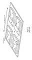
- FIG. 2shows a perspective view of the semiconductor die 100 .
- the die 100is a flash memory die that includes a plurality of flash memory-cell arrays 102 . Each memory-cell array 102 has adjacent associated row-decoder (“X-Dec”) circuitry 104 and an adjacent page buffer 106 .
- the die 100further includes peripheral logic circuitry 108 . As FIG. 2 shows, the memory-cell arrays 102 are higher (e.g., 3-5 um higher) than the peripheral logic circuitry 108 (e.g., at a time during fabrication before a planarizing inter-layer dielectric has been deposited above the circuitry of FIGS. 1 and 2 ).
- the center lines 112 representing the locations on which the inspection tool focusesmay not pass through the row-decoder circuitry 104 .
- the inspection toolmay perform its scans with a focus that is not ideal or even suitable for the row-decoder circuitry 104 , making it difficult or impossible to detect defects in the row-decoder circuitry 104 .
- this problemmay make it necessary to perform multiple passes along each TDI swath 110 using different focus offsets, thus increasing inspection time, decreasing inspection throughput, and increasing the time for setting up inspection recipes.
- a method of semiconductor inspectionis performed at a semiconductor-inspection system.
- user inputis received that specifies a swath across a semiconductor die for inspection.
- the swathhas a width that is less than a width of the semiconductor die and that corresponds to a field of view of the semiconductor-inspection system.
- the swath of the semiconductor dieis inspected based on the user input. Data from inspecting the swath is processed to identify defects in the swath.
- a semiconductor-inspection systemincludes an inspection tool, one or more processors, and memory storing one or more programs for execution by the one or more processors.
- the one or more programsinclude instructions for performing the above method.
- a non-transitory computer-readable storage mediumstores one or more programs for execution by one or more processors of a semiconductor-inspection system that includes an inspection tool.
- the one or more programsinclude instructions for performing the above method.
- FIG. 1shows a plan view of a semiconductor die for which an inspection tool has a fixed layout of time-delay integration (TDI) swaths.
- TDItime-delay integration
- FIG. 2shows a perspective view of the semiconductor die of FIG. 1 that illustrates a height difference between respective portions of the die.
- FIG. 3shows a plan view of a user-selectable layout of swaths for the semiconductor die of FIGS. 1 and 2 in accordance with some embodiments.
- FIG. 4is a flowchart showing a method of semiconductor inspection in accordance with some embodiments.
- FIG. 5is a block diagram of a semiconductor-inspection system in accordance with some embodiments.
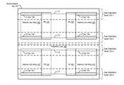
- FIG. 3shows a plan view of a user-selectable layout of swaths 300 (e.g., TDI swaths) for the semiconductor die 100 in accordance with some embodiments.
- the usermay specify the location of each swath 300 - 1 , 300 - 2 , 300 - 3 , and 300 - 4 .
- the swaths 300thus are user-selectable.
- FIG. 3shows a plan view of a user-selectable layout of swaths 300 (e.g., TDI swaths) for the semiconductor die 100 in accordance with some embodiments.
- the usermay specify the location of each swath 300 - 1 , 300 - 2 , 300 - 3 , and 300 - 4 .
- the swaths 300thus are user-selectable.
- FIG. 1shows a plan view of a user-selectable layout of sw
- the userhas specified the locations of the swaths 300 - 1 , 300 - 2 , 300 - 3 , and 300 - 4 such that the center lines 112 of the swaths 300 pass through respective instances of the row-decoder circuitry 104 , thereby allowing the inspection tool to focus on the row-decoder circuitry 104 .
- the inspection toolmay achieve higher quality, more precise inspection results for the row-decoder circuitry 104 .
- FIG. 4is a flowchart showing a method 400 of semiconductor inspection in accordance with some embodiments.
- the method 400may be performed by a semiconductor-inspection system 500 ( FIG. 5 ) that includes a semiconductor inspection tool 504 and associated computer circuitry.
- user inputis received ( 402 ) specifying a swath across a semiconductor die (e.g., semiconductor die 100 , FIGS. 1-3 ) for inspection.
- the semiconductor dieis a flash memory die.
- the dieis another type of semiconductor device.
- the user inputis received through an input device 510 ( FIG. 5 ).
- the user inputwas previously provided and stored as part of a recipe, and is received as part of retrieving the recipe (e.g., from the memory 511 or from a remote computer system communicatively coupled with the semiconductor-inspection system 500 , FIG. 5 ).
- the swath(e.g., swath 300 - 1 , 300 - 2 , 300 - 3 , or 300 - 4 , FIG. 3 ) has a width that is less than a width of the semiconductor die and that corresponds to a field of view of the semiconductor-inspection system (e.g., of the inspection tool 504 , FIG. 5 ).
- the inputspecifies ( 404 ) a point within the swath that corresponds to a line across the swath.
- the inputspecifies a center position within the width of the swath (e.g., by specifying a respective center line 112 or a point on a respective center line 112 , FIG.
- the inputmay specify another position offset above or below the center position within the width of the swath.
- the width of the swathmay be fixed or variable.
- the widthmay have a first value in a first mode of the inspection tool 504 and a second value in a second mode of the inspection tool 504 .
- the first modemay be a normal field-of-view mode (e.g., with a swath width of 550 um) and the second mode may be a reduced field-of-view mode (e.g., with a swath width of 280 um), in accordance with some embodiments.
- the semiconductor dieincludes a first portion having a first height, a second portion having a second height that is less than the first height, and a transition portion between the first portion and the second portion.
- the linepasses ( 406 ) through the transition portion.
- the first portionincludes at least part of an array of flash memory cells (e.g., a memory-cell array 102 , FIG. 3 ) and the second portion includes circuitry peripheral to the array of flash memory cells (e.g., peripheral logic circuitry 108 , FIG. 3 ).
- the transition portionmay include row-decoder circuitry 104 that is adjacent to the array.
- a wafer that contains the semiconductor dieis loaded into the inspection tool 504 .
- the wafermay be loaded before or after the user input is received in step 402 .
- the semiconductor inspection tool 504auto-focuses ( 408 ) on a portion of the swath (e.g., a portion corresponding to the line across the swath, such as the center line 112 ). The user thus may specify the portion on which the semiconductor inspection tool 504 auto-focuses, in accordance with some embodiments.
- a focus offset to be used to inspect the swathis determined ( 410 ). In some other embodiments, the focus offset may have been previously determined and stored as part of a recipe used in the method 400 . In some embodiments (e.g., for which step 406 applies), the semiconductor inspection tool 504 auto-focuses ( 412 ) on the transition portion (e.g., on row-decoder circuitry 104 ).
- the swath of the semiconductor dieis inspected ( 414 ) based on the user input (e.g., in accordance with the auto-focusing).
- time-delay integrationis performed ( 416 ) to inspect the die, such that the swath is a TDI swath.
- the data obtained from inspecting the swathis processed ( 418 ) to identify defects in the swath. For example, data obtained by inspecting the swath is compared to data obtained by inspecting the same swath on other die.
- the swath specified in step 402is a first swath.
- the method 400includes receiving user input specifying a plurality of swaths across the semiconductor die (e.g., all of the swaths 300 - 1 , 300 - 2 , 300 - 3 , and 300 - 4 , FIG. 3 ) for inspection.
- the plurality of swathsincludes the first swath (e.g., swath 300 - 1 , 300 - 2 , 300 - 3 , or 300 - 4 , FIG. 3 ).
- Each swath of the plurality of swathshas a respective width that is less than the width of the semiconductor die.
- Each swath of the plurality of swathsmay have the width of the first swath (e.g., a fixed width corresponding to a field of view of the inspection tool 504 ) or may have one or a plurality of available widths (e.g., with the available widths corresponding to respective modes of the inspection tool 504 ).
- Each swath of the plurality of swathsis inspected based on the user input specifying the plurality of swaths (e.g., in accordance with the auto-focusing).
- the data obtained from inspecting each swathis processed to identify defects in the plurality of swaths.
- the semiconductor dieis a first semiconductor die and the method 400 includes inspecting the specified swath for every semiconductor die in a row or column on the wafer that includes the first semiconductor die (e.g., in a single pass, which may be performed through a single translation of the movable wafer chuck 506 , FIG. 5 ). Furthermore, the specified swath may be inspected for all or a portion of the die on the wafer. The data obtained from inspecting the specified swath on multiple die is processed to identify defects.
- the method 400thus allows accurate inspection of a particular portion of a semiconductor die, by allowing the inspection tool to focus on that portion. Throughput may be increased, by avoiding recipes that perform multiple passes with different focus offsets along the same swath. Similarly, the method 400 may reduce recipe set-up times. Furthermore, the swath or plurality of swaths being inspected may compose only part of the entire die. Throughput thus may also be increased by avoiding inspecting portions of the die that are not of interest.
- FIG. 5is a block diagram of a semiconductor-inspection system 500 in accordance with some embodiments.
- the semiconductor-inspection system 500includes a semiconductor inspection tool 504 and associated computer circuitry, including one or more processors 502 (e.g., CPUs), user interfaces 508 , memory 511 , and one or more communication buses 503 interconnecting these components.
- the semiconductor-inspection system 500may also include one or more network interfaces (wired and/or wireless, not shown) for communicating with (e.g., retrieving recipes from and/or transmitting data to) remote computer systems.
- the inspection tool 504includes an illumination source 505 , a movable wafer chuck 506 , and a TDI senor array 507 .
- Semiconductor wafersare loaded onto the movable wafer chuck 506 , which moves linearly (i.e., is linearly translated) during inspection of a swath, to allow TDI to be performed.
- the illumination source 505is a broadband plasma (BBP) illumination source.
- BBPbroadband plasma
- a different type of illumination source 505e.g., a single-wavelength laser
- the user interfaces 508may include a display 509 and one or more input devices 510 (e.g., a keyboard, mouse, touch-sensitive surface of the display 509 , etc.).
- a usermay use the one or more input devices 510 to specify swaths. For example, an image of a semiconductor die (e.g., the die 100 , FIGS. 1-3 ) may be displayed on the display 509 .
- the usermay draw a center line 112 ( FIG. 3 ) or other line across a swath, select a point corresponding to the center line 112 or other line across the swath, or otherwise provide input indicating the location of the swath.
- Memory 511includes volatile and/or non-volatile memory.
- Memory 511e.g., the non-volatile memory within memory 511
- Memory 511includes a non-transitory computer-readable storage medium.
- Memory 511optionally includes one or more storage devices remotely located from the processors 502 and/or a non-transitory computer-readable storage medium that is removably inserted into the server system 500 .
- memory 511(e.g., the non-transitory computer-readable storage medium of memory 511 ) stores the following modules and data, or a subset or superset thereof: an operating system 512 that includes procedures for handling various basic system services and for performing hardware-dependent tasks, a TDI inspection module 514 (e.g., for performing all or a portion of steps 402 - 416 of the method 400 , FIG. 4 ), and a defect identification module 520 (e.g., for performing step 418 of the method 400 , FIG. 4 ).
- the TDI inspection module 514may include a swath-specification module 516 and/or an auto-focus module 518 , and may store one or more recipes for performing die inspection.
- the memory 511(e.g., the non-transitory computer-readable storage medium of the memory 511 ) thus includes instructions for performing all or a portion of the method 400 ( FIG. 4 ).
- Each of the modules stored in the memory 511corresponds to a set of instructions for performing one or more functions described herein. Separate modules need not be implemented as separate software programs. The modules and various subsets of the modules may be combined or otherwise re-arranged.
- the memory 511stores a subset or superset of the modules and/or data structures identified above.
- FIG. 5is intended more as a functional description of the various features that may be present in a semiconductor-inspection system than as a structural schematic.
- the arrangement of the components of the inspection tool 504may vary (e.g., in manners known in the art). Items shown separately could be combined and some items could be separated.
- the functionality of the semiconductor-inspection system 500may be split between multiple devices. For example, a portion of the modules stored in the memory 511 may alternatively be stored in one or more computer systems communicatively coupled with the semiconductor-inspection system 500 through one or more networks.
Landscapes
- Engineering & Computer Science (AREA)
- Manufacturing & Machinery (AREA)
- Computer Hardware Design (AREA)
- Power Engineering (AREA)
- Microelectronics & Electronic Packaging (AREA)
- Physics & Mathematics (AREA)
- General Physics & Mathematics (AREA)
- Health & Medical Sciences (AREA)
- Biochemistry (AREA)
- Pathology (AREA)
- Immunology (AREA)
- Life Sciences & Earth Sciences (AREA)
- Chemical & Material Sciences (AREA)
- Analytical Chemistry (AREA)
- General Health & Medical Sciences (AREA)
- Signal Processing (AREA)
- Condensed Matter Physics & Semiconductors (AREA)
- Multimedia (AREA)
- Computer Vision & Pattern Recognition (AREA)
- Testing Or Measuring Of Semiconductors Or The Like (AREA)
- Investigating Materials By The Use Of Optical Means Adapted For Particular Applications (AREA)
- Preparing Plates And Mask In Photomechanical Process (AREA)
Abstract
Description
- This application claims priority to U.S. Provisional Patent Application No. 62/573,811, filed Oct. 18, 2017, titled “3D Flash Swath Optimization,” which is hereby incorporated by reference in its entirety.
- This disclosure relates to semiconductor inspection tools, and more specifically to user selection of swaths to be inspected on semiconductor die.
- Semiconductor inspection tools may use time-delay integration (TDI) to inspect semiconductor die, in order to identify defects on the die. Such inspection tools use TDI to scan TDI swaths across the die, with respective TDI swaths being scanned and thus inspected sequentially. The inspection results may be compared to inspection results for other semiconductor die of the same type, to identify defects. Successive scanning of multiple TDI swaths is performed because the field of view of the inspection tool, and thus the TDI swath width, is typically less than the width of the die.
- The swath layout is traditionally fixed for a given semiconductor die. For example,
FIG. 1 shows a plan view of asemiconductor die 100 for which an inspection tool has a fixed layout ofTDI swaths 110, starting from the top of thedie 100. The inspection tool focuses on the center of eachTDI swath 110, as indicated by thecenter lines 112. - Such focusing is problematic, however, because the height of different portions of the
semiconductor die 100 may vary. For example,FIG. 2 shows a perspective view of thesemiconductor die 100. The die100 is a flash memory die that includes a plurality of flash memory-cell arrays 102. Each memory-cell array 102 has adjacent associated row-decoder (“X-Dec”)circuitry 104 and anadjacent page buffer 106. The die100 further includesperipheral logic circuitry 108. AsFIG. 2 shows, the memory-cell arrays 102 are higher (e.g., 3-5 um higher) than the peripheral logic circuitry108 (e.g., at a time during fabrication before a planarizing inter-layer dielectric has been deposited above the circuitry ofFIGS. 1 and 2 ). This height difference exists because the flash memory cells of the memory-cell arrays 102 include oxide-nitride-oxide stacks that are absent from other circuitry such as theperipheral logic circuitry 108. Circuitry immediately adjacent to the memory-cell arrays 102, such as the row-decoder circuitry 104, occupies a transition region in which the die height transitions from a first value for the memory-cell arrays 102 to a second, lower value for theperipheral logic circuitry 108. - As seen in
FIG. 1 , thecenter lines 112 representing the locations on which the inspection tool focuses may not pass through the row-decoder circuitry 104. As a result, the inspection tool may perform its scans with a focus that is not ideal or even suitable for the row-decoder circuitry 104, making it difficult or impossible to detect defects in the row-decoder circuitry 104. Furthermore, this problem may make it necessary to perform multiple passes along eachTDI swath 110 using different focus offsets, thus increasing inspection time, decreasing inspection throughput, and increasing the time for setting up inspection recipes. - Accordingly, there is a need for methods and systems of allowing users to specify swaths for inspection.
- In some embodiments, a method of semiconductor inspection is performed at a semiconductor-inspection system. In the method, user input is received that specifies a swath across a semiconductor die for inspection. The swath has a width that is less than a width of the semiconductor die and that corresponds to a field of view of the semiconductor-inspection system. The swath of the semiconductor die is inspected based on the user input. Data from inspecting the swath is processed to identify defects in the swath.
- In some embodiments, a semiconductor-inspection system includes an inspection tool, one or more processors, and memory storing one or more programs for execution by the one or more processors. The one or more programs include instructions for performing the above method. In some embodiments, a non-transitory computer-readable storage medium stores one or more programs for execution by one or more processors of a semiconductor-inspection system that includes an inspection tool. The one or more programs include instructions for performing the above method.
- For a better understanding of the various described implementations, reference should be made to the Detailed Description below, in conjunction with the following drawings.
FIG. 1 shows a plan view of a semiconductor die for which an inspection tool has a fixed layout of time-delay integration (TDI) swaths.FIG. 2 shows a perspective view of the semiconductor die ofFIG. 1 that illustrates a height difference between respective portions of the die.FIG. 3 shows a plan view of a user-selectable layout of swaths for the semiconductor die ofFIGS. 1 and 2 in accordance with some embodiments.FIG. 4 is a flowchart showing a method of semiconductor inspection in accordance with some embodiments.FIG. 5 is a block diagram of a semiconductor-inspection system in accordance with some embodiments.- Like reference numerals refer to corresponding parts throughout the drawings and specification.
- Reference will now be made in detail to various embodiments, examples of which are illustrated in the accompanying drawings. In the following detailed description, numerous specific details are set forth in order to provide a thorough understanding of the various described embodiments. However, it will be apparent to one of ordinary skill in the art that the various described embodiments may be practiced without these specific details. In other instances, well-known methods, procedures, components, circuits, and networks have not been described in detail so as not to unnecessarily obscure aspects of the embodiments.
- To alleviate the problems caused by the fixed layout of the TDI swaths110 (
FIG. 1 ), an inspection tool may allow the positions of swaths on a die to be user-selectable.FIG. 3 shows a plan view of a user-selectable layout of swaths300 (e.g., TDI swaths) for the semiconductor die100 in accordance with some embodiments. The user may specify the location of each swath300-1,300-2,300-3, and300-4. The swaths300 thus are user-selectable. In the example ofFIG. 3 , the user has specified the locations of the swaths300-1,300-2,300-3, and300-4 such that thecenter lines 112 of the swaths300 pass through respective instances of the row-decoder circuitry 104, thereby allowing the inspection tool to focus on the row-decoder circuitry 104. As a result, the inspection tool may achieve higher quality, more precise inspection results for the row-decoder circuitry 104. FIG. 4 is a flowchart showing amethod 400 of semiconductor inspection in accordance with some embodiments. Themethod 400 may be performed by a semiconductor-inspection system500 (FIG. 5 ) that includes asemiconductor inspection tool 504 and associated computer circuitry.- In the
method 400, user input is received (402) specifying a swath across a semiconductor die (e.g.,semiconductor die 100,FIGS. 1-3 ) for inspection. In some embodiments, the semiconductor die is a flash memory die. Alternatively, the die is another type of semiconductor device. In some embodiments, the user input is received through an input device510 (FIG. 5 ). Alternatively, the user input was previously provided and stored as part of a recipe, and is received as part of retrieving the recipe (e.g., from thememory 511 or from a remote computer system communicatively coupled with the semiconductor-inspection system 500,FIG. 5 ). - The swath (e.g., swath300-1,300-2,300-3, or300-4,
FIG. 3 ) has a width that is less than a width of the semiconductor die and that corresponds to a field of view of the semiconductor-inspection system (e.g., of theinspection tool 504,FIG. 5 ). In some embodiments, the input specifies (404) a point within the swath that corresponds to a line across the swath. For example, the input specifies a center position within the width of the swath (e.g., by specifying arespective center line 112 or a point on arespective center line 112,FIG. 3 ). In other examples, the input may specify another position offset above or below the center position within the width of the swath. The width of the swath may be fixed or variable. For example, the width may have a first value in a first mode of theinspection tool 504 and a second value in a second mode of theinspection tool 504. The first mode may be a normal field-of-view mode (e.g., with a swath width of 550 um) and the second mode may be a reduced field-of-view mode (e.g., with a swath width of 280 um), in accordance with some embodiments. - In some embodiments, the semiconductor die includes a first portion having a first height, a second portion having a second height that is less than the first height, and a transition portion between the first portion and the second portion. The line passes (406) through the transition portion. For example, the first portion includes at least part of an array of flash memory cells (e.g., a memory-
cell array 102,FIG. 3 ) and the second portion includes circuitry peripheral to the array of flash memory cells (e.g.,peripheral logic circuitry 108,FIG. 3 ). In this example, the transition portion may include row-decoder circuitry 104 that is adjacent to the array. - A wafer that contains the semiconductor die is loaded into the
inspection tool 504. The wafer may be loaded before or after the user input is received in step402. - In some embodiments, the
semiconductor inspection tool 504 auto-focuses (408) on a portion of the swath (e.g., a portion corresponding to the line across the swath, such as the center line112). The user thus may specify the portion on which thesemiconductor inspection tool 504 auto-focuses, in accordance with some embodiments. In some embodiments, a focus offset to be used to inspect the swath is determined (410). In some other embodiments, the focus offset may have been previously determined and stored as part of a recipe used in themethod 400. In some embodiments (e.g., for which step406 applies), thesemiconductor inspection tool 504 auto-focuses (412) on the transition portion (e.g., on row-decoder circuitry104). - The swath of the semiconductor die is inspected (414) based on the user input (e.g., in accordance with the auto-focusing). In some embodiments, time-delay integration is performed (416) to inspect the die, such that the swath is a TDI swath.
- The data obtained from inspecting the swath is processed (418) to identify defects in the swath. For example, data obtained by inspecting the swath is compared to data obtained by inspecting the same swath on other die.
- In some embodiments, the swath specified in step402 is a first swath. The
method 400 includes receiving user input specifying a plurality of swaths across the semiconductor die (e.g., all of the swaths300-1,300-2,300-3, and300-4,FIG. 3 ) for inspection. The plurality of swaths includes the first swath (e.g., swath300-1,300-2,300-3, or300-4,FIG. 3 ). Each swath of the plurality of swaths has a respective width that is less than the width of the semiconductor die. Each swath of the plurality of swaths may have the width of the first swath (e.g., a fixed width corresponding to a field of view of the inspection tool504) or may have one or a plurality of available widths (e.g., with the available widths corresponding to respective modes of the inspection tool504). - Each swath of the plurality of swaths is inspected based on the user input specifying the plurality of swaths (e.g., in accordance with the auto-focusing). The data obtained from inspecting each swath is processed to identify defects in the plurality of swaths.
- In some embodiments, the semiconductor die is a first semiconductor die and the
method 400 includes inspecting the specified swath for every semiconductor die in a row or column on the wafer that includes the first semiconductor die (e.g., in a single pass, which may be performed through a single translation of themovable wafer chuck 506,FIG. 5 ). Furthermore, the specified swath may be inspected for all or a portion of the die on the wafer. The data obtained from inspecting the specified swath on multiple die is processed to identify defects. - The
method 400 thus allows accurate inspection of a particular portion of a semiconductor die, by allowing the inspection tool to focus on that portion. Throughput may be increased, by avoiding recipes that perform multiple passes with different focus offsets along the same swath. Similarly, themethod 400 may reduce recipe set-up times. Furthermore, the swath or plurality of swaths being inspected may compose only part of the entire die. Throughput thus may also be increased by avoiding inspecting portions of the die that are not of interest. FIG. 5 is a block diagram of a semiconductor-inspection system 500 in accordance with some embodiments. The semiconductor-inspection system 500 includes asemiconductor inspection tool 504 and associated computer circuitry, including one or more processors502 (e.g., CPUs), user interfaces508,memory 511, and one ormore communication buses 503 interconnecting these components. The semiconductor-inspection system 500 may also include one or more network interfaces (wired and/or wireless, not shown) for communicating with (e.g., retrieving recipes from and/or transmitting data to) remote computer systems.- The
inspection tool 504 includes anillumination source 505, amovable wafer chuck 506, and aTDI senor array 507. Semiconductor wafers are loaded onto themovable wafer chuck 506, which moves linearly (i.e., is linearly translated) during inspection of a swath, to allow TDI to be performed. In some embodiments, theillumination source 505 is a broadband plasma (BBP) illumination source. Alternatively, a different type of illumination source505 (e.g., a single-wavelength laser) is used. - The user interfaces508 may include a
display 509 and one or more input devices510 (e.g., a keyboard, mouse, touch-sensitive surface of thedisplay 509, etc.). A user may use the one ormore input devices 510 to specify swaths. For example, an image of a semiconductor die (e.g., thedie 100,FIGS. 1-3 ) may be displayed on thedisplay 509. The user may draw a center line112 (FIG. 3 ) or other line across a swath, select a point corresponding to thecenter line 112 or other line across the swath, or otherwise provide input indicating the location of the swath. Memory 511 includes volatile and/or non-volatile memory. Memory511 (e.g., the non-volatile memory within memory511) includes a non-transitory computer-readable storage medium.Memory 511 optionally includes one or more storage devices remotely located from theprocessors 502 and/or a non-transitory computer-readable storage medium that is removably inserted into theserver system 500. In some embodiments, memory511 (e.g., the non-transitory computer-readable storage medium of memory511) stores the following modules and data, or a subset or superset thereof: anoperating system 512 that includes procedures for handling various basic system services and for performing hardware-dependent tasks, a TDI inspection module514 (e.g., for performing all or a portion of steps402-416 of themethod 400,FIG. 4 ), and a defect identification module520 (e.g., for performingstep 418 of themethod 400,FIG. 4 ). The TDI inspection module514 may include a swath-specification module 516 and/or an auto-focus module518, and may store one or more recipes for performing die inspection.- The memory511 (e.g., the non-transitory computer-readable storage medium of the memory511) thus includes instructions for performing all or a portion of the method400 (
FIG. 4 ). Each of the modules stored in thememory 511 corresponds to a set of instructions for performing one or more functions described herein. Separate modules need not be implemented as separate software programs. The modules and various subsets of the modules may be combined or otherwise re-arranged. In some embodiments, thememory 511 stores a subset or superset of the modules and/or data structures identified above. FIG. 5 is intended more as a functional description of the various features that may be present in a semiconductor-inspection system than as a structural schematic. For example, the arrangement of the components of theinspection tool 504 may vary (e.g., in manners known in the art). Items shown separately could be combined and some items could be separated. Furthermore, the functionality of the semiconductor-inspection system 500 may be split between multiple devices. For example, a portion of the modules stored in thememory 511 may alternatively be stored in one or more computer systems communicatively coupled with the semiconductor-inspection system 500 through one or more networks.- The foregoing description, for purpose of explanation, has been described with reference to specific embodiments. However, the illustrative discussions above are not intended to be exhaustive or to limit the scope of the claims to the precise forms disclosed. Many modifications and variations are possible in view of the above teachings. The embodiments were chosen in order to best explain the principles underlying the claims and their practical applications, to thereby enable others skilled in the art to best use the embodiments with various modifications as are suited to the particular uses contemplated.
Claims (17)
Priority Applications (4)
| Application Number | Priority Date | Filing Date | Title |
|---|---|---|---|
| US16/128,367US11222799B2 (en) | 2017-10-18 | 2018-09-11 | Swath selection for semiconductor inspection |
| PCT/US2018/055791WO2019079139A1 (en) | 2017-10-18 | 2018-10-15 | Swath selection for semiconductor inspection |
| CN201880068021.3ACN111316411B (en) | 2017-10-18 | 2018-10-15 | Strip Selection for Semiconductor Inspection |
| KR1020207013982AKR20200059308A (en) | 2017-10-18 | 2018-10-15 | Swath selection for semiconductor inspection |
Applications Claiming Priority (2)
| Application Number | Priority Date | Filing Date | Title |
|---|---|---|---|
| US201762573811P | 2017-10-18 | 2017-10-18 | |
| US16/128,367US11222799B2 (en) | 2017-10-18 | 2018-09-11 | Swath selection for semiconductor inspection |
Publications (2)
| Publication Number | Publication Date |
|---|---|
| US20190115236A1true US20190115236A1 (en) | 2019-04-18 |
| US11222799B2 US11222799B2 (en) | 2022-01-11 |
Family
ID=66097100
Family Applications (1)
| Application Number | Title | Priority Date | Filing Date |
|---|---|---|---|
| US16/128,367Active2038-10-17US11222799B2 (en) | 2017-10-18 | 2018-09-11 | Swath selection for semiconductor inspection |
Country Status (4)
| Country | Link |
|---|---|
| US (1) | US11222799B2 (en) |
| KR (1) | KR20200059308A (en) |
| CN (1) | CN111316411B (en) |
| WO (1) | WO2019079139A1 (en) |
Cited By (2)
| Publication number | Priority date | Publication date | Assignee | Title |
|---|---|---|---|---|
| WO2021087014A1 (en)* | 2019-10-31 | 2021-05-06 | Kla Corporation | Bbp assisted defect detection flow for sem images |
| US20240068967A1 (en)* | 2022-08-25 | 2024-02-29 | Kla Corporation | Noise diagnostics for an electron beam inspection system with swathing |
Families Citing this family (1)
| Publication number | Priority date | Publication date | Assignee | Title |
|---|---|---|---|---|
| US20240412944A1 (en)* | 2023-06-08 | 2024-12-12 | Kla Corporation | Autofocus method for single beam and multi-beam systems |
Citations (6)
| Publication number | Priority date | Publication date | Assignee | Title |
|---|---|---|---|---|
| US6867406B1 (en)* | 1999-03-23 | 2005-03-15 | Kla-Tencor Corporation | Confocal wafer inspection method and apparatus using fly lens arrangement |
| US20050249395A1 (en)* | 2004-05-04 | 2005-11-10 | Kla-Tencor Technologies Corporation | High throughput image for processing inspection images |
| US20070288219A1 (en)* | 2005-11-18 | 2007-12-13 | Khurram Zafar | Methods and systems for utilizing design data in combination with inspection data |
| US20120205546A1 (en)* | 2011-02-14 | 2012-08-16 | Kla-Tencor Corporation | Optical imaging system with laser droplet plasma illuminator |
| US20140105482A1 (en)* | 2012-10-15 | 2014-04-17 | Kla-Tencor Corporation | Detecting Defects on a Wafer Using Defect-Specific Information |
| US20150029499A1 (en)* | 2013-07-25 | 2015-01-29 | Kla-Tencor Corporation | Auto-focus system and methods for die-to-die inspection |
Family Cites Families (15)
| Publication number | Priority date | Publication date | Assignee | Title |
|---|---|---|---|---|
| US5450205A (en)* | 1993-05-28 | 1995-09-12 | Massachusetts Institute Of Technology | Apparatus and method for real-time measurement of thin film layer thickness and changes thereof |
| US6020957A (en) | 1998-04-30 | 2000-02-01 | Kla-Tencor Corporation | System and method for inspecting semiconductor wafers |
| US6828647B2 (en)* | 2001-04-05 | 2004-12-07 | Infineon Technologies Ag | Structure for determining edges of regions in a semiconductor wafer |
| CN1518085B (en)* | 2003-01-15 | 2010-05-12 | 内格夫技术有限公司 | High-speed in-line electro-optics testing method and system for defects on chip |
| US7227984B2 (en) | 2003-03-03 | 2007-06-05 | Kla-Tencor Technologies Corporation | Method and apparatus for identifying defects in a substrate surface by using dithering to reconstruct under-sampled images |
| US7063990B2 (en)* | 2003-09-04 | 2006-06-20 | Eastman Kodak Company | Inspecting swath boundaries produced by thermal transfer of organic materials in forming OLED devices |
| DE102004055250A1 (en)* | 2004-11-16 | 2006-05-18 | Leica Microsystems Semiconductor Gmbh | Method for inspecting a wafer |
| US8041103B2 (en) | 2005-11-18 | 2011-10-18 | Kla-Tencor Technologies Corp. | Methods and systems for determining a position of inspection data in design data space |
| JP2009192371A (en) | 2008-02-14 | 2009-08-27 | Tokyo Seimitsu Co Ltd | Visual examination device and visual examination method |
| US7973921B2 (en) | 2008-06-25 | 2011-07-05 | Applied Materials South East Asia Pte Ltd. | Dynamic illumination in optical inspection systems |
| NL2005332A (en)* | 2009-10-13 | 2011-04-14 | Asml Netherlands Bv | Inspection method and apparatus. |
| US8658987B2 (en)* | 2010-02-22 | 2014-02-25 | Hitachi High-Technologies Corporation | Circuit-pattern inspection device |
| US8772731B2 (en) | 2012-04-15 | 2014-07-08 | Kla-Tencor Corporation | Apparatus and method for synchronizing sample stage motion with a time delay integration charge-couple device in a semiconductor inspection tool |
| KR102618495B1 (en)* | 2015-01-18 | 2023-12-29 | 삼성전자주식회사 | Apparatus and method for processing image |
| US9816940B2 (en) | 2015-01-21 | 2017-11-14 | Kla-Tencor Corporation | Wafer inspection with focus volumetric method |
- 2018
- 2018-09-11USUS16/128,367patent/US11222799B2/enactiveActive
- 2018-10-15CNCN201880068021.3Apatent/CN111316411B/enactiveActive
- 2018-10-15WOPCT/US2018/055791patent/WO2019079139A1/ennot_activeCeased
- 2018-10-15KRKR1020207013982Apatent/KR20200059308A/ennot_activeWithdrawn
Patent Citations (6)
| Publication number | Priority date | Publication date | Assignee | Title |
|---|---|---|---|---|
| US6867406B1 (en)* | 1999-03-23 | 2005-03-15 | Kla-Tencor Corporation | Confocal wafer inspection method and apparatus using fly lens arrangement |
| US20050249395A1 (en)* | 2004-05-04 | 2005-11-10 | Kla-Tencor Technologies Corporation | High throughput image for processing inspection images |
| US20070288219A1 (en)* | 2005-11-18 | 2007-12-13 | Khurram Zafar | Methods and systems for utilizing design data in combination with inspection data |
| US20120205546A1 (en)* | 2011-02-14 | 2012-08-16 | Kla-Tencor Corporation | Optical imaging system with laser droplet plasma illuminator |
| US20140105482A1 (en)* | 2012-10-15 | 2014-04-17 | Kla-Tencor Corporation | Detecting Defects on a Wafer Using Defect-Specific Information |
| US20150029499A1 (en)* | 2013-07-25 | 2015-01-29 | Kla-Tencor Corporation | Auto-focus system and methods for die-to-die inspection |
Cited By (4)
| Publication number | Priority date | Publication date | Assignee | Title |
|---|---|---|---|---|
| WO2021087014A1 (en)* | 2019-10-31 | 2021-05-06 | Kla Corporation | Bbp assisted defect detection flow for sem images |
| US11450012B2 (en) | 2019-10-31 | 2022-09-20 | Kla Corporation | BBP assisted defect detection flow for SEM images |
| US20240068967A1 (en)* | 2022-08-25 | 2024-02-29 | Kla Corporation | Noise diagnostics for an electron beam inspection system with swathing |
| US12372486B2 (en)* | 2022-08-25 | 2025-07-29 | Kla Corporation | Noise diagnostics for an electron beam inspection system with swathing |
Also Published As
| Publication number | Publication date |
|---|---|
| WO2019079139A1 (en) | 2019-04-25 |
| KR20200059308A (en) | 2020-05-28 |
| CN111316411A (en) | 2020-06-19 |
| US11222799B2 (en) | 2022-01-11 |
| CN111316411B (en) | 2023-10-31 |
Similar Documents
| Publication | Publication Date | Title |
|---|---|---|
| US11222799B2 (en) | Swath selection for semiconductor inspection | |
| US10964014B2 (en) | Defect detecting method and defect detecting system | |
| US7657077B2 (en) | Detecting defects by three-way die-to-die comparison with false majority determination | |
| US12039716B2 (en) | Defect inspection method and defect inspection device | |
| KR20230111273A (en) | Method for inspecting substrate, substrate treatment system, and computer storage medium | |
| US20060280358A1 (en) | Pattern comparison inspection method and pattern comparison inspection device | |
| TW202024612A (en) | Super-resolution defect review image generation through generative adversarial networks | |
| CN112635346B (en) | Wafer inspection method, semiconductor inspection apparatus, and storage medium | |
| WO2020179000A1 (en) | Defect inspection device and defect inspection program | |
| US20150146967A1 (en) | Pattern evaluation device and pattern evaluation method | |
| CN112789713B (en) | Semiconductor wafer defect inspection system and method for aligning semiconductor wafer image | |
| US10359706B1 (en) | Integrated scanning electron microscopy and optical analysis techniques for advanced process control | |
| CN113725112B (en) | Wafer detection method, system and detection machine | |
| CN112368569A (en) | Multi-mode defect classification in semiconductor inspection | |
| US8692878B2 (en) | Methods and apparatus for simultaneously inspecting multiple array regions having different pitches | |
| TW202208837A (en) | Scanning electron microscope image anchoring to design for array | |
| JP6906044B2 (en) | Systems and methods that use the z-layer context in logical and hotspot inspection for sensitivity improvement and nuance suppression | |
| US6011619A (en) | Semiconductor wafer optical scanning system and method using swath-area defect limitation | |
| KR20220070459A (en) | Equal probability defect detection | |
| KR102606069B1 (en) | Wafer inspection method | |
| US20170256070A1 (en) | Inspection method and system and a method of inspecting a semiconductor device using the same | |
| KR20210000317A (en) | Improved target selection to improve design alignment | |
| KR20120129302A (en) | Wafer defect high speed inspection apparatus | |
| JP2009188175A (en) | External appearance inspecting apparatus and method | |
| JP2009192371A (en) | Visual examination device and visual examination method |
Legal Events
| Date | Code | Title | Description |
|---|---|---|---|
| AS | Assignment | Owner name:KLA-TENCOR CORPORATION, CALIFORNIA Free format text:ASSIGNMENT OF ASSIGNORS INTEREST;ASSIGNOR:KANG, BOSUK;REEL/FRAME:046845/0708 Effective date:20180910 | |
| FEPP | Fee payment procedure | Free format text:ENTITY STATUS SET TO UNDISCOUNTED (ORIGINAL EVENT CODE: BIG.); ENTITY STATUS OF PATENT OWNER: LARGE ENTITY | |
| STPP | Information on status: patent application and granting procedure in general | Free format text:APPLICATION DISPATCHED FROM PREEXAM, NOT YET DOCKETED | |
| STPP | Information on status: patent application and granting procedure in general | Free format text:DOCKETED NEW CASE - READY FOR EXAMINATION | |
| STPP | Information on status: patent application and granting procedure in general | Free format text:NON FINAL ACTION MAILED | |
| STPP | Information on status: patent application and granting procedure in general | Free format text:FINAL REJECTION MAILED | |
| STPP | Information on status: patent application and granting procedure in general | Free format text:RESPONSE TO NON-FINAL OFFICE ACTION ENTERED AND FORWARDED TO EXAMINER | |
| STPP | Information on status: patent application and granting procedure in general | Free format text:FINAL REJECTION MAILED | |
| STPP | Information on status: patent application and granting procedure in general | Free format text:RESPONSE AFTER FINAL ACTION FORWARDED TO EXAMINER | |
| STPP | Information on status: patent application and granting procedure in general | Free format text:RESPONSE TO NON-FINAL OFFICE ACTION ENTERED AND FORWARDED TO EXAMINER | |
| STPP | Information on status: patent application and granting procedure in general | Free format text:NON FINAL ACTION MAILED | |
| STPP | Information on status: patent application and granting procedure in general | Free format text:RESPONSE TO NON-FINAL OFFICE ACTION ENTERED AND FORWARDED TO EXAMINER | |
| STPP | Information on status: patent application and granting procedure in general | Free format text:NOTICE OF ALLOWANCE MAILED -- APPLICATION RECEIVED IN OFFICE OF PUBLICATIONS | |
| STPP | Information on status: patent application and granting procedure in general | Free format text:PUBLICATIONS -- ISSUE FEE PAYMENT VERIFIED | |
| STCF | Information on status: patent grant | Free format text:PATENTED CASE | |
| MAFP | Maintenance fee payment | Free format text:PAYMENT OF MAINTENANCE FEE, 4TH YEAR, LARGE ENTITY (ORIGINAL EVENT CODE: M1551); ENTITY STATUS OF PATENT OWNER: LARGE ENTITY Year of fee payment:4 |