US20180366355A1 - Substrate processing systems, apparatus, and methods with factory interface environmental controls - Google Patents
Substrate processing systems, apparatus, and methods with factory interface environmental controlsDownload PDFInfo
- Publication number
- US20180366355A1 US20180366355A1US16/112,197US201816112197AUS2018366355A1US 20180366355 A1US20180366355 A1US 20180366355A1US 201816112197 AUS201816112197 AUS 201816112197AUS 2018366355 A1US2018366355 A1US 2018366355A1
- Authority
- US
- United States
- Prior art keywords
- factory interface
- electronic device
- chamber
- processing system
- device processing
- Prior art date
- Legal status (The legal status is an assumption and is not a legal conclusion. Google has not performed a legal analysis and makes no representation as to the accuracy of the status listed.)
- Granted
Links
Images


Classifications
- H—ELECTRICITY
- H01—ELECTRIC ELEMENTS
- H01L—SEMICONDUCTOR DEVICES NOT COVERED BY CLASS H10
- H01L21/00—Processes or apparatus adapted for the manufacture or treatment of semiconductor or solid state devices or of parts thereof
- H01L21/67—Apparatus specially adapted for handling semiconductor or electric solid state devices during manufacture or treatment thereof; Apparatus specially adapted for handling wafers during manufacture or treatment of semiconductor or electric solid state devices or components ; Apparatus not specifically provided for elsewhere
- H01L21/67005—Apparatus not specifically provided for elsewhere
- H01L21/67011—Apparatus for manufacture or treatment
- H01L21/67155—Apparatus for manufacturing or treating in a plurality of work-stations
- H01L21/67207—Apparatus for manufacturing or treating in a plurality of work-stations comprising a chamber adapted to a particular process
- H—ELECTRICITY
- H01—ELECTRIC ELEMENTS
- H01L—SEMICONDUCTOR DEVICES NOT COVERED BY CLASS H10
- H01L21/00—Processes or apparatus adapted for the manufacture or treatment of semiconductor or solid state devices or of parts thereof
- H01L21/67—Apparatus specially adapted for handling semiconductor or electric solid state devices during manufacture or treatment thereof; Apparatus specially adapted for handling wafers during manufacture or treatment of semiconductor or electric solid state devices or components ; Apparatus not specifically provided for elsewhere
- H01L21/677—Apparatus specially adapted for handling semiconductor or electric solid state devices during manufacture or treatment thereof; Apparatus specially adapted for handling wafers during manufacture or treatment of semiconductor or electric solid state devices or components ; Apparatus not specifically provided for elsewhere for conveying, e.g. between different workstations
- H01L21/67763—Apparatus specially adapted for handling semiconductor or electric solid state devices during manufacture or treatment thereof; Apparatus specially adapted for handling wafers during manufacture or treatment of semiconductor or electric solid state devices or components ; Apparatus not specifically provided for elsewhere for conveying, e.g. between different workstations the wafers being stored in a carrier, involving loading and unloading
- H01L21/67772—Apparatus specially adapted for handling semiconductor or electric solid state devices during manufacture or treatment thereof; Apparatus specially adapted for handling wafers during manufacture or treatment of semiconductor or electric solid state devices or components ; Apparatus not specifically provided for elsewhere for conveying, e.g. between different workstations the wafers being stored in a carrier, involving loading and unloading involving removal of lid, door, cover
- H—ELECTRICITY
- H01—ELECTRIC ELEMENTS
- H01L—SEMICONDUCTOR DEVICES NOT COVERED BY CLASS H10
- H01L21/00—Processes or apparatus adapted for the manufacture or treatment of semiconductor or solid state devices or of parts thereof
- H01L21/67—Apparatus specially adapted for handling semiconductor or electric solid state devices during manufacture or treatment thereof; Apparatus specially adapted for handling wafers during manufacture or treatment of semiconductor or electric solid state devices or components ; Apparatus not specifically provided for elsewhere
- H01L21/67005—Apparatus not specifically provided for elsewhere
- H01L21/67011—Apparatus for manufacture or treatment
- H01L21/67017—Apparatus for fluid treatment
- H—ELECTRICITY
- H01—ELECTRIC ELEMENTS
- H01L—SEMICONDUCTOR DEVICES NOT COVERED BY CLASS H10
- H01L21/00—Processes or apparatus adapted for the manufacture or treatment of semiconductor or solid state devices or of parts thereof
- H01L21/67—Apparatus specially adapted for handling semiconductor or electric solid state devices during manufacture or treatment thereof; Apparatus specially adapted for handling wafers during manufacture or treatment of semiconductor or electric solid state devices or components ; Apparatus not specifically provided for elsewhere
- H01L21/67005—Apparatus not specifically provided for elsewhere
- H01L21/67242—Apparatus for monitoring, sorting or marking
- H01L21/67248—Temperature monitoring
- H—ELECTRICITY
- H01—ELECTRIC ELEMENTS
- H01L—SEMICONDUCTOR DEVICES NOT COVERED BY CLASS H10
- H01L21/00—Processes or apparatus adapted for the manufacture or treatment of semiconductor or solid state devices or of parts thereof
- H01L21/67—Apparatus specially adapted for handling semiconductor or electric solid state devices during manufacture or treatment thereof; Apparatus specially adapted for handling wafers during manufacture or treatment of semiconductor or electric solid state devices or components ; Apparatus not specifically provided for elsewhere
- H01L21/67005—Apparatus not specifically provided for elsewhere
- H01L21/67242—Apparatus for monitoring, sorting or marking
- H01L21/67253—Process monitoring, e.g. flow or thickness monitoring
Definitions
- Embodimentsrelates to electronic device manufacturing, and more specifically to equipment front end modules (EFEMs), and apparatus, systems, and methods for processing of substrates.
- EFEMsequipment front end modules
- Electronic device manufacturing systemsmay include multiple process chambers arranged around a mainframe housing having a transfer chamber and one or more load lock chambers configured to pass substrates into the transfer chamber. These systems may employ a transfer robot, which may be housed in the transfer chamber, for example.
- the transfer robotmay be a selectively compliant articulated robot arm (SCARA) robot or the like, and may be adapted to transport substrates between the various chambers and one or more load lock chambers.
- SCARAselectively compliant articulated robot arm
- the transfer robotmay transport substrates from process chamber to process chamber, from load lock chamber to process chamber, and vice versa.
- Processing of substrates in semi-conductor component manufacturingis generally carried out in multiple tools, where the substrates travel between the tools in substrate carriers (e.g., Front Opening Unified Pods or FOUPs).
- the FOUPsmay be docked to an EFEM (sometimes referred to as a “factory interface or FI”), which includes a load/unload robot therein that is operable to transfer substrates between the FOUPs and the one or more load locks of the tool therefore allowing pass through of substrates for processing.
- EFEMFront Opening Unified Pods
- FIfront Opening Unified Pods
- an electronic device processing systemincludes a factory interface including a factory interface chamber, a load lock apparatus coupled to the factory interface, one or more substrate carriers coupled to the factory interface, and an environmental control system coupled to the factory interface and operational to monitor or control one of: a relative humidity, a temperature, an amount of O 2 , or an amount of an inert gas, within the factory interface chamber.
- a method of processing substrates within an electronic device processing systemincludes providing a factory interface including a factory interface chamber, one or more substrate carriers docked to the factory interface, a load lock apparatus including one or more load lock chambers coupled to the factory interface, and possibly an access door, and controlling environmental conditions in the factory interface chamber to meet environmental preconditions.
- a method of processing substrates within an electronic device processing systemincludes providing a factory interface including a factory interface chamber, one or more substrate carriers docked to the factory interface, one or more carrier purge chambers within the factory interface chamber, and one or more load lock chambers coupled to the factory interface, and controlling environmental conditions in the factory interface chamber and the one or more carrier purge chambers.
- FIG. 1illustrates a schematic top view of an electronic device processing system including factory interface environmental controls according to embodiments.
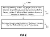
- FIG. 2illustrates a flowchart depicting a method of processing substrates within an electronic device processing system according to embodiments.
- FIG. 3illustrates a schematic top view of an electronic device processing system including an inert gas recirculation system according to embodiments.
- FIG. 4illustrates a schematic top view of another electronic device processing system including environmental controls and inert gas recirculation according to embodiments.
- FIG. 5Aillustrates a cross-sectioned side view of a carrier purge assembly according to embodiments.
- FIG. 5Billustrates a front view of a carrier purge assembly according to embodiments.
- FIG. 6illustrates another flowchart depicting a method of processing substrates within an electronic device processing system according to embodiments.
- Electronic device manufacturingmay desire very precise processing, as well as rapid transport of substrates between various locations.
- existing systemsmay transfer substrates between FOUPs and load locks and then into processing chambers.
- existing systemsmay suffer from problems when relatively higher humidity, temperature, or other environmental factors, such as too high of an oxygen (O 2 ) level are observed.
- O 2oxygen
- exposure to relatively high humidity levels or relatively high O 2 levelsmay adversely affect substrate properties.
- electronic device processing systemsadapted to provide improved substrate processing are provided.
- the systems and methods described hereinmay provide efficiency and/or processing improvements in the processing of substrates by controlling environmental conditions within a factory interface chamber of the factory interface.
- the factory interfacereceives substrates from one or more substrate carriers docked to the factory interface (e.g., docked to a front surface thereof and a load/unload robot delivers the substrates to one or more load locks coupled on another surface of the factory interface (e.g., a rear surface thereof).
- one or more environmental parameterse.g., a relative humidity, a temperature, an amount of O 2 , or an amount of an inert gas
- one or more load locks or any FOUP docked to the factory interfacemay be opened unless certain pre-conditions regarding the environment in a factory interface chamber of the factory interface are met.
- FIGS. 1-6Further details of example method and apparatus embodiments of the invention are described with reference to FIGS. 1-6 herein.
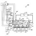
- FIG. 1is a schematic diagram of an example embodiment of an electronic device processing system 100 according to one or more embodiments of the present invention.
- the electronic device processing system 100may include a mainframe housing 101 having housing walls defining a transfer chamber 102 .
- a transfer robot 103(shown as a dotted circle) may be at least partially housed within the transfer chamber 102 .
- the transfer robot 103may be configured and adapted to place or extract substrates to and from destinations via operation of the arms of the transfer robot 103 .
- Substrates as used hereinshall mean articles used to make electronic devices or circuit components, such as silica-containing wafers, patterned wafers, or the like.
- Transfer robot 103may be any suitable type of off-axis robot adapted to service the various twin chambers coupled to and accessible from the transfer chamber 102 , such as the robot disclosed in US Patent Pub. No. 2010/0178147, for example.
- Other off-axis robotsmay be used.
- An off-axis robotis any robot configuration that can operate to extend an end effector other than radially towards or away from a shoulder rotational axis of the robot, which is generally centered at the center of the transfer chamber 102 .
- the motion of the various arm components of the transfer robot 103may be controlled by suitable commands to a drive assembly (not shown) containing a plurality of drive motors of the transfer robot 103 as commanded from a controller 125 . Signals from the controller 125 may cause motion of the various components of the transfer robot 103 . Suitable feedback mechanisms may be provided for one or more of the components by various sensors, such as position encoders, or the like.
- the transfer robot 103may include arms rotatable about a shoulder axis, which may be approximately centrally located in the transfer chamber 102 .
- Transfer robot 103may include a base that is adapted to be attached to a housing wall (e.g., a floor) forming a lower portion of the transfer chamber 102 .
- the transfer robot 103may be attached to a ceiling in some embodiments.
- the robot 103may be a dual SCARA robot or other type of dual robot adapted to service twin chambers (e.g., side-by-side chambers). Other types of process chamber orientations, as well as transfer robots may be used.
- the rotation of the arm components of the transfer robot 103may be provided by any suitable drive motor, such as a conventional variable reluctance or permanent magnet electric motor. Arms may be adapted to be rotated in an X-Y plane relative to the base. Any suitable number of arm components and end effectors adapted to carry the substrates may be used.
- the drive assembly of the transfer robot 103may include Z-axis motion capability in some embodiments.
- the motor housingmay be restrained from rotation relative to an outer casing by a motion restrictor.
- Motion restrictormay be two or more linear bearings or other type of bearing or slide mechanisms that function to constrain rotation of the motor housing relative to the outer casing, yet allow Z-axis (vertical) motion of the motor housing and connected arms along the vertical direction.
- the vertical motionmay be provided by a vertical motor. Rotation of the vertical motor may operate to rotate a lead screw in a receiver coupled to or integral with motor housing. This rotation may vertically translate the motor housing, and, thus, the arms, one or more attached end effectors, and the substrates supported thereon.
- a suitable sealmay seal between the motor housing and the base thereby accommodating the vertical motion, and retaining a vacuum within the transfer chamber 102 in some embodiments.
- the transfer chamber 102 in the depicted embodimentmay be generally square or slightly rectangular in shape and may include a first facet 102 A, second facet 102 B opposite the first facet 102 A, a third facet 102 C, and a fourth facet 102 D opposite the third facet 102 C.
- the transfer robot 103may be preferably adept at transferring and/or retracting dual substrates at a same time into the chamber sets.
- the first facet 102 A, second facet 102 B, a third facet 102 C, and fourth facet 102 Dmay be generally planar and entryways into the chamber sets may lie along the respective facets.
- other suitable shape of the mainframe housing 101 and numbers of facets and processing chambersis possible.
- the destinations for the transfer robot 103may be a first process chamber set 108 A, 108 B, coupled to the first facet 102 A and which may be configured and operable to carry out a process on the substrates delivered thereto.
- the processmay be any suitable process such as plasma vapor deposition (PVD) or chemical vapor deposition (CVD), etch, annealing, pre-clean, metal ore metal oxide removal, or the like. Other processes may be carried out on substrates therein.
- the destinations for the transfer robot 103may also be a second process chamber set 108 C, 108 D that may be generally opposed from the first process chamber set 108 A, 108 B.
- the second process chamber set 108 C, 108 Dmay be coupled to the second facet 102 B and may be configured and adapted to carry out any suitable process on the substrates, such as any of the processes mentioned above.
- the destinations for the transfer robot 103may also be a third process chamber set 108 E, 108 F that may be generally opposed from the load lock apparatus 112 coupled to the third facet 102 C.
- the third process chamber set 108 E, 108 Fmay be configured and adapted to carry out any suitable process on the substrates, such as any of the processes mentioned above.
- Substratesmay be received into the transfer chamber 102 from a factory interface 114 , and also exit the transfer chamber 102 , to the factory interface 114 , through the load lock apparatus 112 that is coupled to a surface (e.g., a rear wall) of the factory interface 114 .
- the load lock apparatus 112may include one or more load lock chambers (e.g., load lock chambers 112 A, 112 B, for example).
- Load lock chambers 112 A, 112 B that are included in the load lock apparatus 112may be single wafer load locks (SWLL) chambers, or multi-wafer chambers.
- SWLLsingle wafer load locks
- the load lock apparatus 112may, in some embodiments, include a heating platform/apparatus to heat the substrate to greater than about 200 degrees C., such that a degassing process may be carried out on incoming substrates before they are passed into the transfer chamber 102 from the factory interface 114 .
- the factory interface 114may be any enclosure having sidewall surfaces (including front, rear, two side walls, a top, and a bottom) forming a factory interface chamber 114 C.
- One or more load ports 115may be provided on surfaces (e.g., front surfaces) of the factory interface 114 and may be configured and adapted to receive one or more substrate carriers 116 (e.g., front opening unified pods or FOUPs) thereat.
- substrate carriers 116e.g., front opening unified pods or FOUPs
- Factory interface 114may include a suitable load/unload robot 117 (shown dotted) of conventional construction within the factory interface chamber 114 C thereof.
- the load/unload robot 117may be configured and operational, once the doors of the substrate carriers 116 are opened, to extract substrates from the one or more substrate carriers 116 and feed the substrates through the factory interface chamber 114 C and into the one or more load lock chambers 112 A, 112 B as may be provided in the load lock apparatus 112 .
- Any suitable construction of the load lock apparatus 112allowing transfer of substrates between the transfer chamber 102 and the factory interface chamber 114 C may be used.
- the transfer chamber 102may include slit valves 134 at an ingress/egress to the various process chambers 108 A through 108 F.
- load lock chambers 112 A, 112 B in the one or more load lock apparatus 112may include inner and outer load lock slit valves 136 , 138 .
- Slit valves 134 , 136 , 138are adapted to open and close when placing or extracting substrates to and from the various process chambers 108 A- 108 F and load lock chambers 112 A, 112 B.
- Slit valves 134 , 136 , 138may be of any suitable conventional construction, such as L-motion slit valves.
- the factory interface chamber 114 Cmay be provided with environmental controls providing an environmentally-controlled atmosphere.
- environmental control system 118is coupled to the factory interface 114 and operational to monitor and/or control environmental conditions within the factory interface chamber 114 C.
- the factory interface chamber 114 Cmay receive an insert gas therein, such as Argon (Ar), Nitrogen (N 2 ), or helium (He), from an inert gas supply 118 A.
- aire.g., filtered air
- airmay be provided from an air supply 118 B.
- the environmental control system 118may control at least one of: 1) relative humidity (RH), 2) temperature (T), 3) an amount of O 2 , or 4) an amount of inert gas, within the factory interface chamber 114 C.
- Other environmental conditions of the factory interfacemay be monitored and/or controlled, such as gas flow rate or pressure or both.
- environmental control system 118includes a controller 125 .
- Controller 125may include suitable processor, memory, and electronic components for receiving inputs from various sensors and controlling one or more valves.
- Environmental control system 118may, in one or more embodiments, monitor relative humidity (RH) by sensing RH in the factory interface chamber 114 C with a relative humidity sensor 130 that is configured and adapted to sense relative humidity (RH). Any suitable type of relative humidity sensor 130 may be used, such as a capacitive-type sensor.
- the controller 125monitors RH, and when a measured RH value provided to the controller 125 is above a predefined RH threshold value, carrier doors 116 D of the one or more substrate carriers 116 coupled to load ports of the factory interface 114 stay closed.
- Carrier doors 116 D of the substrate carriers 116may be opened when the measured RH value falls below the predefined RH threshold value.
- the RHmay be lowered by flowing a suitable amount of an inert gas from the inert gas supply 118 A of the environmental control system 118 into the factory interface chamber 114 C.
- the inert gas from the inert gas supply 118 Amay be argon, N 2 , helium, or mixtures thereof.
- a supply of dry nitrogen gas (N 2 )may be quite effective.
- Compressed bulk inert gases having low H 2 O levels(e.g., less than 5 ppm) may be used as the inert gas supply 118 A in the environmental control system 118 .
- the environmental control system 118measures a relative humidity value with the relative humidity sensor 130 , and if the measured relative humidity value is above a pre-defined reference relative humidity value, an outer load lock slit valve 138 of the one or more load lock apparatus 112 coupled to the factory interface 114 stay closed. The one or more load lock apparatus 112 may remain closed until the relative humidity falls below the pre-defined reference relative humidity value.
- the RHmay be lowered by a control signal from the controller 125 to the environmental control system 118 initiating a flow of a suitable amount of an inert gas from the inert gas supply 118 A into the factory interface chamber 114 C.
- the pre-defined reference relative humidity valuemay be less than 1000 ppm moisture, less than 500 ppm moisture, or even less than 100 ppm moisture, depending upon the level of moisture that is tolerable for the particular process being carried out in the electronic device processing system 100 .
- the environmental control system 118 of the electronic device processing system 100may include an air supply 118 B coupled to the factory interface chamber 114 C.
- the air supply 118 Bmay be coupled by suitable conduits and one or more valves to the factory interface chamber 114 C.
- the environmental control system 118may include an oxygen sensor 132 that is configured and adapted to sense a level of oxygen (O 2 ) within the factory interface chamber 114 C.
- O 2level of oxygen
- the controller 125 of the environmental control system 118may initiate a flow of air from the air supply 118 B such that at least some of the inert gas environment is exhausted and replaced with air.
- a door interlock 140 keeping an access door 142 closedmay be unlatched to allow the access door 142 to be opened (as shown dotted) and thus allow the person access to the factory interface chamber 114 C.
- the factory interface 114 of the electronic device processing system 100may include a cooling station 144 .
- the cooling station 144may include one or more platforms, shelves, or other support features upon which one or more substrates 145 exiting the load lock apparatus 112 may rest and be cooled before insertion into a substrate carrier 116 .
- a temperature sensor 135that is configured and adapted to sense a temperature within the factory interface chamber 114 C may be used.
- the temperature sensor 135may be placed close to the substrate 145 .
- the temperature sensor 135may be a directional sensor, such as a laser sensor that may be used to determine an extent to which the substrate 145 has been cooled. This input from the temperature sensor 135 may be used to determine when the transfer from the cooling station 144 may occur.
- the controller 125may be any suitable controller having suitable processor, memory, and peripheral components adapted to receive control inputs from the various sensors (e.g., relative humidity sensor 130 , oxygen sensor 132 , and/or temperature sensor 135 ) and execute a closed loop or other suitable control scheme.
- the control schememay change a flow rate of a gas being introduced into the factory interface chamber 114 C.
- the control schememay determine when to transfer substrates 145 into the factory interface chamber 114 C.
- the method 200includes, in 202 , providing a factory interface (e.g., factory interface 114 ) having a factory interface chamber (e.g., factory interface chamber 114 C) and one or more substrate carriers (e.g., substrate carriers 116 ) docked to the factory interface, and one or more load lock chambers (e.g., load lock chambers 112 A, 112 B) coupled to the factory interface.
- a factory interfacee.g., factory interface 114
- a factory interface chambere.g., factory interface chamber 114 C
- substrate carrierse.g., substrate carriers 116
- load lock chamberse.g., load lock chambers 112 A, 112 B
- the method 200includes, in 204 , controlling environmental conditions to meet environmental preconditions.
- controlling environmental conditions to meet environmental preconditionsmay take place before opening any one of the one or more substrate carrier doors (e.g., carrier doors 116 D) or the one or more load lock chambers (e.g., opening the outer load lock slit valves 138 of the load lock chambers 112 A, 112 B).
- one or more of the carrier doors 116 D and the outer load lock slit valves 138may be opened when certain environmental preconditions are met.
- environmental preconditionsmay be met, in one example, when a measured relative humidity (RH) level in the factory interface chamber 114 C falls below a predefined relative humidity level threshold (e.g., less than 1000 ppm moisture, less than 500 ppm moisture, less than 100 ppm moisture, or even lower).
- RHrelative humidity
- an inert gase.g., dry N 2 gas or other inert gas
- the inert gas supply 118 Amay be a suitable canister of inert gas under pressure, for example.
- Flow rates of inert gas provided into the factory interface chamber 114 Cmay be monitored by a suitable flow sensor (not shown) on a delivery line and/or pressure sensor 133 located within the factory interface chamber 114 C, or both.
- Flow rates of 400 SLM or moremay be provided by adjusting a valve coupled to the inert gas supply 118 A responsive to control signals provided by controller 125 .
- Pressures of greater than about 500 Pamay be maintained within the factory interface chamber 114 C.
- Flow of inert gas (e.g., N 2 or other inert gas) into the factory interface chamber 114 Cis operative to lower the relative humidity (RH) level, and the carrier door 116 D and/or the outer load lock slit valves 138 of the one or more load lock chambers 112 A, 112 B may be opened when the relative humidity threshold value if met. This helps to ensure that substrates within the substrate carriers 116 that are opened, any load lock chambers 112 A, 112 B that are opened, as well as any substrates passing through the factory interface chamber 114 C are exposed to only a suitably low humidity environment.
- inert gase.g., N 2 or other inert gas
- environmental preconditionsmay be met, for example, when a measured oxygen (O 2 ) level in the factory interface chamber 114 C, as sensed by oxygen sensor 132 , falls below a predefined oxygen threshold level (e.g., less than 50 ppm O 2 , less than 10 ppm O 2 , less than 5 ppm O 2 , or even less than 3 ppm O 2 , or even lower).
- a predefined oxygen threshold levele.g., less than 50 ppm O 2 , less than 10 ppm O 2 , less than 5 ppm O 2 , or even less than 3 ppm O 2 , or even lower.
- Other suitable oxygen level thresholdsmay be used, depending on the processing taking place.
- the controller 125will initiate a control signal to the valve coupled to the inert gas supply 118 A and flow inert gas into the factory interface chamber 114 C until the predefined oxygen threshold level is met, as determined by the controller 125 .
- the carrier door 116 D and/or the outer load lock slit valves 138 of the one or more load lock chambers 112 A, 112 Bmay be opened. This helps to ensure that substrates within the substrate carriers 116 that are opened, any load lock chambers 112 A, 112 B that are opened, as well as any substrates passing through the factory interface chamber 114 C are exposed to relatively low oxygen levels.
- environmental preconditionsmay be met, for example, when a measured temperature level in the factory interface chamber 114 C, such as a temperature of substrates 145 in the cooling station 144 , as sensed by temperature sensor 135 , fall below a predefined temperature threshold level (e.g., less than 100 degrees C., or even lower).
- a predefined temperature threshold levele.g., less than 100 degrees C., or even lower.
- cooled substrates 145may be loaded into a substrate carrier 116 for transport.
- Cooling station 144may include cooling platforms, inert gas flow, or combinations thereof.
- an access door 142 of the factory interface 114may be opened only when certain environmental preconditions are met.
- the environmental preconditionsmay include attaining an oxygen value in the factory interface chamber 114 C that is above a predetermined oxygen level value that has been determined to be safe.
- the oxygen level valuemay be sensed by the oxygen sensor 132 , for example.
- a door interlock 140e.g., an electromechanical lock
- Air supply 118 Bmay be a supply of filtered air provided by a fan or air pump.
- the environmental control system 318 of the electronic device processing system 300may include the components previously mentioned, but may also include inert gas recirculation. In particular, the inert gas may be recycled and reused in order to provide more efficient environmental controls of the factory interface 114 .
- the inert gas from the factory interface chamber 114 Cmay be exhausted in an exhaust conduit 350 from the factory interface chamber 114 C, filtered through a filter 352 , which may be a moisture-reducing filter and also may filter particulates, and then may be pumped back into the inert gas supply 118 A by a pump 354 .
- the filter 352may be a moisture absorbent filter, which may include multiple layers of absorbent materials. However, other mechanisms or devices for reducing moisture content, such as condensers or other moisture removers may be used.
- the inert gasmay also be cooled.
- Inert gas consumptionmay be monitored in some embodiments, such as by use of a flow sensor (not shown) in the delivery line from the inter gas supply 118 A and the measured flow rate may be correlated to attaining a specified RH value within the factory interface chamber 114 C. If the amount of inert gas consumption is outside of a pre-established limit, then a leak in the factory interface chamber 114 C may be flagged, such as by an message to an operator, a visual indicator, an alarm, or the like. Optionally, if a pressure within the factory interface chamber 114 C is outside (e.g., below) a pre-established limit, then a leak in the factory interface chamber 114 C may be flagged, as above.
- FIG. 4illustrates another embodiment of electronic device processing system 400 including an environmental control system 418 .
- the environmental control system 418includes a combination of environmental control of the factory interface chamber 414 C coupled with environmental control of one or more carrier purge chambers 454 .
- this embodimentis similar to the FIG. 3 embodiment, except that a carrier purge system 452 is provided.
- Carrier purge system 452which may be capable of independent usage apart from the environmental control of the factory interface chamber 414 C, includes a gas purge system 457 .
- Gas purge system 457includes the inert gas supply (e.g., inert gas supply 118 A) and a plurality of supply conduits and valves coupled thereto.
- the plurality of supply conduits and valves of the gas purge system 457supply inert gas to the carrier purge chambers 454 at certain times responsive to control signals from the controller 425 .
- the supply of inert gasmay be provided to a carrier purge chamber 454 just after opening a carrier door 116 D of a substrate carrier 116 in order to purge the environment 562 ( FIG. 5A ) of the substrate carrier 116 and the carrier purge chamber 454 to meet certain environmental preconditions before transferring substrates 545 from the substrate carrier 116 into the factory interface chamber 114 C.
- Carrier purge system 452includes a carrier purge housing 556 for each substrate carrier 116 including purge capability. Such purge capability may be included for some or all of the substrate carriers 116 .
- Carrier purge housing 556forms a part of each carrier purge chamber 454 .
- Carrier purge housing 556may seal against a surface of an inside wall 558 of the factory interface 114 (e.g., a front wall) and form the carrier purge chamber 454 .
- Carrier purge housing 556remains sealed against the surface of an inside wall 558 as the carrier door 116 D is opened. Any suitable seal may be used, such as a gasket or O-ring.
- the carrier purge system 452is adapted to receive the environment 562 of the substrate carrier 116 into a carrier purge chamber 454 upon opening a carrier door 116 D thereof via operation of a door opener 565 and the door retraction mechanism 567 . Once the carrier door 116 D is opened, purging of the carrier purge chamber 454 may take place so that the environment 562 , which may contain undesirable levels of O 2 or moisture, does not enter the factory interface chamber 114 C. Purging of the carrier purge chamber 454 continues until certain predefined environmental conditions are met. Purging may be provided via inert gas provided from the gas purge system 457 .
- One or more diffusers 559may be included at the exits from a conduit 557 C of the gas purge system 457 supplying inert gas into the carrier purge chamber 454 .
- the environmental conditionsmay be based upon a predefined relative humidity RH threshold level and/or a predefined O 2 threshold level, for example.
- a relative humidity of less than a predefined RH threshold levele.g., less than about 5% moisture-less than about 50,000 ppm
- a relative humidity of less than a predefined RH threshold levelmay be sought before retracting the carrier purge housing 556 away from the inside wall 558 and lowering the carrier purge housing 556 to allow the load/unload robot 117 to access and remove the substrates 545 .
- an O 2 threshold level of less than a predefined threshold levele.g., less than about 500 ppm O 2
- Other predefined threshold levelsmay be used.
- a chamber relative humidity sensor 576 and/or a chamber oxygen sensor 578may be provided that interconnect with the controller 425 .
- Chamber relative humidity sensor 576 and/or a chamber oxygen sensor 578may be on the carrier purge housing 556 , in a chamber exhaust conduit 580 within the factory interface chamber 114 C, or even outside of the factory interface 114 , such as on the chamber exhaust conduit 580 .
- Purging with inert gas from the gas purge system 457may continue until the environmental preconditions are met.
- purging for a certain pre-established time or volumemay be used to ensure that the environmental preconditions are met.
- the carrier purge housing 556surrounds a door opener 565 .
- the door opener 565is adapted to be retractable within an interior of the carrier purge housing 556 .
- Retraction of the door opener 565may be by a door retraction mechanism 567 , such as a linear slide 569 and a rack and pinion mechanism 570 .
- Rack and pinion mechanism 570may include a rack 572 , pinion 574 , and drive motor 575 coupled to the pinion 574 .
- Drive signals from the controller 425 to the drive motor 575causes retraction of the carrier door 116 D and mixing of the environment 562 with that in the carrier purge chamber 454 .
- Any door unlock and grasp mechanism 573may be used on the door opener 565 to grasp and open the carrier door 116 D, as is conventional.
- Retraction from and closure (e.g., sealing) against the inside wall 558 by the carrier purge housing 556may be provided by a housing drive system 581 and slide mechanism 582 .
- Slide mechanism 582allows linear motion towards and away from the inside wall 558 relative to a support frame 584 that attaches to an elevator 585 .
- Housing drive system 581may include a suitable motor and transmission mechanism to cause the motion towards and away from the inside wall 558 .
- a rack and pinion mechanismis shown, including housing rack 586 coupled to the carrier purge housing 556 , housing pinion 588 , and housing drive motor 589 .
- Driving the housing drive motor 589translates the carrier purge housing 556 horizontally in or out relative to the elevator 585 and the inside wall 558 .
- Elevator 585may include any suitable mechanism construction for providing vertical motion of the carrier purge housing 556 .
- the elevator 585includes a linear bearing assembly 590 including a bearing slide 591 , rail 592 , and mounting blocks 593 .
- Mounting blocks 593may fasten the rail 592 to the inside wall 558 .
- Bearing slide 591may fasten to a vertical actuator 594 .
- a Vertical actuator rail 595may also be provided, and may be fastened to the inside wall 558 . Actuation of the vertical actuator 594 causes vertical motion relative to the vertical actuator rail 595 , raising or lowering the support frame 584 and the coupled carrier purge housing 556 .
- Vertical actuator 594may be any suitable actuator type, such as pneumatic, electrical, or the like.
- operation of the door grasp and unlock mechanism 573grasps and opens the carrier door 116 D
- the rack and pinion mechanism 570retracts the carrier door 116 D
- the carrier purge system 452purges the carrier purge chamber 454 to meet environmental preconditions
- the housing drive system 581retracts the carrier purge housing 556
- the elevator 585lowers the carrier purge housing 556 and carrier door 116 D so that the load/unload robot 117 may access the substrates 545 in the substrate carrier 116 .
- the environmental control system 418may include the components previously mentioned, and may also include inert gas recirculation.
- the inert gasmay be exhausted in an exhaust conduit 450 from the factory interface chamber 414 C, and filtered through filter 352 , which may be a moisture-reducing filter, but may also filter particulates, and may be of the type discussed above.
- the filtered inert gasmay be recirculated directly back into the factory interface chamber 414 C.
- a portion of the exhaust circulation routemay be through the chamber door 442 .
- the exhaust from the factory interface chamber 414 Cmay enter into a channel 443 (e.g., a duct) formed in the chamber door 442 .
- Channel 443may have an entrance from the factory interface chamber 414 C at or near a bottom of the chamber door 442 , and progress to above the filter 352 , which may be within an upper part of the factory interface chamber 414 C in some embodiments.
- channel 443may be part of the exhaust conduit 450 .
- a door similar to chamber door 442 including an internal channel, like channel 443may be provided on the other side of the factory interface 414 in some embodiments.
- the method 600includes, in 602 , providing a factory interface (e.g., factory interface 414 ) having a factory interface chamber (e.g., factory interface chamber 414 C), one or more substrate carriers (e.g., substrate carriers 116 ) docked to the factory interface, one or more carrier purge chambers (e.g., carrier purge chambers 454 ) within the factory interface chamber, and one or more load lock chambers (e.g., load lock chambers 112 A, 112 B of load lock apparatus 112 ) coupled to the factory interface.
- a factory interfacee.g., factory interface 414
- a factory interface chambere.g., factory interface chamber 414 C
- substrate carrierse.g., substrate carriers 116
- carrier purge chamberse.g., carrier purge chambers 454
- load lock chamberse.g., load lock chambers 112 A, 112 B of load lock apparatus 112
- the method 600includes, in 604 , controlling environmental conditions within the factory interface (e.g., factory interface 414 ) and within the one or more carrier purge chambers (e.g., carrier purge chambers 454 ).
- Controlling environmental conditions within the factory interfacemay include meeting environmental preconditions in the factory interface chamber before allowing the opening any one of the one or more substrate carrier doors (e.g., carrier doors 116 D) or any one of the one or more load lock chambers (e.g., the outer load lock slit valves 138 of the load lock chambers 112 A, 112 B).
- Controlling environmental conditions within the one or more carrier purge chambersmay include meeting certain environmental preconditions (e.g., on RH threshold level or an O 2 threshold level) before unsealing via retraction and lowering the carrier purge housing 556 , as discussed above.
- Providing such environmental controls in accordance with embodiments of the inventionmay reduce exposure of the substrates 545 exiting the substrate carriers 116 or exiting the load lock chambers 112 A, 112 B after processing to environmental conditions that may be detrimental, such as relatively humid environments or environments with relatively high O 2 levels.
Landscapes
- Engineering & Computer Science (AREA)
- Manufacturing & Machinery (AREA)
- Computer Hardware Design (AREA)
- Power Engineering (AREA)
- Microelectronics & Electronic Packaging (AREA)
- General Physics & Mathematics (AREA)
- Physics & Mathematics (AREA)
- Condensed Matter Physics & Semiconductors (AREA)
- Container, Conveyance, Adherence, Positioning, Of Wafer (AREA)
- Drying Of Semiconductors (AREA)
- Exposure Of Semiconductors, Excluding Electron Or Ion Beam Exposure (AREA)
- Cleaning Or Drying Semiconductors (AREA)
- Automation & Control Theory (AREA)
Abstract
Description
- This application is a continuation application of, and claims priority to U.S. patent application Ser. No. 14/456,631, filed Aug. 11, 2014, titled “SUBSTRATE PROCESSING SYSTEMS, APPARATUS, AND METHODS WITH FACTORY INTERFACE ENVIRONMENTAL CONTROLS” (Attorney Docket No. 21149/USA), which claims priority to and the benefit of U.S. Provisional Patent Application No. 61/865,046, filed Aug. 12, 2013, titled “SUBSTRATE PROCESSING SYSTEMS, APPARATUS, AND METHODS WITH FACTORY INTERFACE ENVIRONMENTAL CONTROLS” (Attorney Docket No. 21149/USA/L), each of which is hereby incorporated by reference herein in its entirety for all purposes.
- Embodiments relates to electronic device manufacturing, and more specifically to equipment front end modules (EFEMs), and apparatus, systems, and methods for processing of substrates.
- Electronic device manufacturing systems may include multiple process chambers arranged around a mainframe housing having a transfer chamber and one or more load lock chambers configured to pass substrates into the transfer chamber. These systems may employ a transfer robot, which may be housed in the transfer chamber, for example. The transfer robot may be a selectively compliant articulated robot arm (SCARA) robot or the like, and may be adapted to transport substrates between the various chambers and one or more load lock chambers. For example, the transfer robot may transport substrates from process chamber to process chamber, from load lock chamber to process chamber, and vice versa.
- Processing of substrates in semi-conductor component manufacturing is generally carried out in multiple tools, where the substrates travel between the tools in substrate carriers (e.g., Front Opening Unified Pods or FOUPs). The FOUPs may be docked to an EFEM (sometimes referred to as a “factory interface or FI”), which includes a load/unload robot therein that is operable to transfer substrates between the FOUPs and the one or more load locks of the tool therefore allowing pass through of substrates for processing. Existing systems may benefit from efficiency and/or process quality improvements.
- Accordingly, systems, apparatus, and methods having improved efficiency and/or capability in the processing of substrates are desired.
- In one aspect, an electronic device processing system is provided. The electronic device processing system includes a factory interface including a factory interface chamber, a load lock apparatus coupled to the factory interface, one or more substrate carriers coupled to the factory interface, and an environmental control system coupled to the factory interface and operational to monitor or control one of: a relative humidity, a temperature, an amount of O2, or an amount of an inert gas, within the factory interface chamber.
- In another aspect, a method of processing substrates within an electronic device processing system is provided. The method includes providing a factory interface including a factory interface chamber, one or more substrate carriers docked to the factory interface, a load lock apparatus including one or more load lock chambers coupled to the factory interface, and possibly an access door, and controlling environmental conditions in the factory interface chamber to meet environmental preconditions.
- In yet another method aspect, a method of processing substrates within an electronic device processing system is provided. The method includes providing a factory interface including a factory interface chamber, one or more substrate carriers docked to the factory interface, one or more carrier purge chambers within the factory interface chamber, and one or more load lock chambers coupled to the factory interface, and controlling environmental conditions in the factory interface chamber and the one or more carrier purge chambers.
- Numerous other aspects are provided in accordance with these and other embodiments of the invention. Other features and aspects of embodiments of the present invention will become more fully apparent from the following detailed description, the appended claims, and the accompanying drawings.
- The drawings, described below, are for illustrative purposes only and are not necessarily drawn to scale. The drawings are not intended to limit the scope of the invention in any way.
FIG. 1 illustrates a schematic top view of an electronic device processing system including factory interface environmental controls according to embodiments.FIG. 2 illustrates a flowchart depicting a method of processing substrates within an electronic device processing system according to embodiments.FIG. 3 illustrates a schematic top view of an electronic device processing system including an inert gas recirculation system according to embodiments.FIG. 4 illustrates a schematic top view of another electronic device processing system including environmental controls and inert gas recirculation according to embodiments.FIG. 5A illustrates a cross-sectioned side view of a carrier purge assembly according to embodiments.FIG. 5B illustrates a front view of a carrier purge assembly according to embodiments.FIG. 6 illustrates another flowchart depicting a method of processing substrates within an electronic device processing system according to embodiments.- Reference will now be made in detail to the example embodiments of this disclosure, which are illustrated in the accompanying drawings. Wherever possible, the same reference numbers will be used throughout the drawings to refer to the same or like parts throughout the several views. Features of the various embodiments described herein may be combined with each other, unless specifically noted otherwise.
- Electronic device manufacturing may desire very precise processing, as well as rapid transport of substrates between various locations. In particular, existing systems may transfer substrates between FOUPs and load locks and then into processing chambers. However, existing systems may suffer from problems when relatively higher humidity, temperature, or other environmental factors, such as too high of an oxygen (O2) level are observed. In particular, exposure to relatively high humidity levels or relatively high O2levels may adversely affect substrate properties.
- According to one or more embodiments of the invention, electronic device processing systems adapted to provide improved substrate processing are provided. The systems and methods described herein may provide efficiency and/or processing improvements in the processing of substrates by controlling environmental conditions within a factory interface chamber of the factory interface. The factory interface receives substrates from one or more substrate carriers docked to the factory interface (e.g., docked to a front surface thereof and a load/unload robot delivers the substrates to one or more load locks coupled on another surface of the factory interface (e.g., a rear surface thereof). In some embodiments, one or more environmental parameters (e.g., a relative humidity, a temperature, an amount of O2, or an amount of an inert gas) are monitored, and neither the one or more load locks or any FOUP docked to the factory interface may be opened unless certain pre-conditions regarding the environment in a factory interface chamber of the factory interface are met.
- Further details of example method and apparatus embodiments of the invention are described with reference to
FIGS. 1-6 herein. FIG. 1 is a schematic diagram of an example embodiment of an electronicdevice processing system 100 according to one or more embodiments of the present invention. The electronicdevice processing system 100 may include amainframe housing 101 having housing walls defining atransfer chamber 102. A transfer robot103 (shown as a dotted circle) may be at least partially housed within thetransfer chamber 102. Thetransfer robot 103 may be configured and adapted to place or extract substrates to and from destinations via operation of the arms of thetransfer robot 103. Substrates as used herein shall mean articles used to make electronic devices or circuit components, such as silica-containing wafers, patterned wafers, or the like.Transfer robot 103, in the depicted embodiment, may be any suitable type of off-axis robot adapted to service the various twin chambers coupled to and accessible from thetransfer chamber 102, such as the robot disclosed in US Patent Pub. No. 2010/0178147, for example. Other off-axis robots may be used. An off-axis robot is any robot configuration that can operate to extend an end effector other than radially towards or away from a shoulder rotational axis of the robot, which is generally centered at the center of thetransfer chamber 102.- The motion of the various arm components of the
transfer robot 103 may be controlled by suitable commands to a drive assembly (not shown) containing a plurality of drive motors of thetransfer robot 103 as commanded from acontroller 125. Signals from thecontroller 125 may cause motion of the various components of thetransfer robot 103. Suitable feedback mechanisms may be provided for one or more of the components by various sensors, such as position encoders, or the like. - The
transfer robot 103 may include arms rotatable about a shoulder axis, which may be approximately centrally located in thetransfer chamber 102.Transfer robot 103 may include a base that is adapted to be attached to a housing wall (e.g., a floor) forming a lower portion of thetransfer chamber 102. However, thetransfer robot 103 may be attached to a ceiling in some embodiments. Therobot 103 may be a dual SCARA robot or other type of dual robot adapted to service twin chambers (e.g., side-by-side chambers). Other types of process chamber orientations, as well as transfer robots may be used. - The rotation of the arm components of the
transfer robot 103 may be provided by any suitable drive motor, such as a conventional variable reluctance or permanent magnet electric motor. Arms may be adapted to be rotated in an X-Y plane relative to the base. Any suitable number of arm components and end effectors adapted to carry the substrates may be used. - Additionally, the drive assembly of the
transfer robot 103 may include Z-axis motion capability in some embodiments. In particular, the motor housing may be restrained from rotation relative to an outer casing by a motion restrictor. Motion restrictor may be two or more linear bearings or other type of bearing or slide mechanisms that function to constrain rotation of the motor housing relative to the outer casing, yet allow Z-axis (vertical) motion of the motor housing and connected arms along the vertical direction. The vertical motion may be provided by a vertical motor. Rotation of the vertical motor may operate to rotate a lead screw in a receiver coupled to or integral with motor housing. This rotation may vertically translate the motor housing, and, thus, the arms, one or more attached end effectors, and the substrates supported thereon. A suitable seal may seal between the motor housing and the base thereby accommodating the vertical motion, and retaining a vacuum within thetransfer chamber 102 in some embodiments. - The
transfer chamber 102 in the depicted embodiment may be generally square or slightly rectangular in shape and may include afirst facet 102A,second facet 102B opposite thefirst facet 102A, athird facet 102C, and afourth facet 102D opposite thethird facet 102C. Thetransfer robot 103 may be preferably adept at transferring and/or retracting dual substrates at a same time into the chamber sets. Thefirst facet 102A,second facet 102B, athird facet 102C, andfourth facet 102D may be generally planar and entryways into the chamber sets may lie along the respective facets. However, other suitable shape of themainframe housing 101 and numbers of facets and processing chambers is possible. - The destinations for the
transfer robot 103 may be a first process chamber set108A,108B, coupled to thefirst facet 102A and which may be configured and operable to carry out a process on the substrates delivered thereto. The process may be any suitable process such as plasma vapor deposition (PVD) or chemical vapor deposition (CVD), etch, annealing, pre-clean, metal ore metal oxide removal, or the like. Other processes may be carried out on substrates therein. - The destinations for the
transfer robot 103 may also be a second process chamber set108C,108D that may be generally opposed from the first process chamber set108A,108B. The second process chamber set108C,108D may be coupled to thesecond facet 102B and may be configured and adapted to carry out any suitable process on the substrates, such as any of the processes mentioned above. Likewise, the destinations for thetransfer robot 103 may also be a third process chamber set108E,108F that may be generally opposed from theload lock apparatus 112 coupled to thethird facet 102C. The third process chamber set108E,108F may be configured and adapted to carry out any suitable process on the substrates, such as any of the processes mentioned above. - Substrates may be received into the
transfer chamber 102 from afactory interface 114, and also exit thetransfer chamber 102, to thefactory interface 114, through theload lock apparatus 112 that is coupled to a surface (e.g., a rear wall) of thefactory interface 114. Theload lock apparatus 112 may include one or more load lock chambers (e.g.,load lock chambers Load lock chambers load lock apparatus 112 may be single wafer load locks (SWLL) chambers, or multi-wafer chambers. Theload lock apparatus 112 may, in some embodiments, include a heating platform/apparatus to heat the substrate to greater than about 200 degrees C., such that a degassing process may be carried out on incoming substrates before they are passed into thetransfer chamber 102 from thefactory interface 114. - The
factory interface 114 may be any enclosure having sidewall surfaces (including front, rear, two side walls, a top, and a bottom) forming afactory interface chamber 114C. One ormore load ports 115 may be provided on surfaces (e.g., front surfaces) of thefactory interface 114 and may be configured and adapted to receive one or more substrate carriers116 (e.g., front opening unified pods or FOUPs) thereat. Factory interface 114 may include a suitable load/unload robot117 (shown dotted) of conventional construction within thefactory interface chamber 114C thereof. The load/unloadrobot 117 may be configured and operational, once the doors of thesubstrate carriers 116 are opened, to extract substrates from the one ormore substrate carriers 116 and feed the substrates through thefactory interface chamber 114C and into the one or moreload lock chambers load lock apparatus 112. Any suitable construction of theload lock apparatus 112 allowing transfer of substrates between thetransfer chamber 102 and thefactory interface chamber 114C may be used.- The
transfer chamber 102 may include slitvalves 134 at an ingress/egress to thevarious process chambers 108A through108F. Likewise,load lock chambers load lock apparatus 112 may include inner and outer load lock slitvalves Slit valves various process chambers 108A-108F and loadlock chambers Slit valves - In the depicted embodiment, the
factory interface chamber 114C may be provided with environmental controls providing an environmentally-controlled atmosphere. In particular,environmental control system 118 is coupled to thefactory interface 114 and operational to monitor and/or control environmental conditions within thefactory interface chamber 114C. In some embodiments, and at certain times, thefactory interface chamber 114C may receive an insert gas therein, such as Argon (Ar), Nitrogen (N2), or helium (He), from aninert gas supply 118A. In other embodiments, or at other times, air (e.g., filtered air) may be provided from anair supply 118B. - In more detail, the
environmental control system 118 may control at least one of: 1) relative humidity (RH), 2) temperature (T), 3) an amount of O2, or 4) an amount of inert gas, within thefactory interface chamber 114C. Other environmental conditions of the factory interface may be monitored and/or controlled, such as gas flow rate or pressure or both. - In some embodiments,
environmental control system 118 includes acontroller 125.Controller 125 may include suitable processor, memory, and electronic components for receiving inputs from various sensors and controlling one or more valves.Environmental control system 118 may, in one or more embodiments, monitor relative humidity (RH) by sensing RH in thefactory interface chamber 114C with arelative humidity sensor 130 that is configured and adapted to sense relative humidity (RH). Any suitable type ofrelative humidity sensor 130 may be used, such as a capacitive-type sensor. In some embodiments, thecontroller 125 monitors RH, and when a measured RH value provided to thecontroller 125 is above a predefined RH threshold value,carrier doors 116D of the one ormore substrate carriers 116 coupled to load ports of thefactory interface 114 stay closed.Carrier doors 116D of thesubstrate carriers 116 may be opened when the measured RH value falls below the predefined RH threshold value. The RH may be lowered by flowing a suitable amount of an inert gas from theinert gas supply 118A of theenvironmental control system 118 into thefactory interface chamber 114C. As described herein, the inert gas from theinert gas supply 118A may be argon, N2, helium, or mixtures thereof. A supply of dry nitrogen gas (N2) may be quite effective. Compressed bulk inert gases having low H2O levels (e.g., less than 5 ppm) may be used as theinert gas supply 118A in theenvironmental control system 118. - In another aspect, the
environmental control system 118 measures a relative humidity value with therelative humidity sensor 130, and if the measured relative humidity value is above a pre-defined reference relative humidity value, an outer load lock slitvalve 138 of the one or moreload lock apparatus 112 coupled to thefactory interface 114 stay closed. The one or moreload lock apparatus 112 may remain closed until the relative humidity falls below the pre-defined reference relative humidity value. As discussed above, the RH may be lowered by a control signal from thecontroller 125 to theenvironmental control system 118 initiating a flow of a suitable amount of an inert gas from theinert gas supply 118A into thefactory interface chamber 114C. In one or more embodiments, the pre-defined reference relative humidity value may be less than 1000 ppm moisture, less than 500 ppm moisture, or even less than 100 ppm moisture, depending upon the level of moisture that is tolerable for the particular process being carried out in the electronicdevice processing system 100. - In some embodiments, the
environmental control system 118 of the electronicdevice processing system 100 may include anair supply 118B coupled to thefactory interface chamber 114C. Theair supply 118B may be coupled by suitable conduits and one or more valves to thefactory interface chamber 114C. Theenvironmental control system 118 may include anoxygen sensor 132 that is configured and adapted to sense a level of oxygen (O2) within thefactory interface chamber 114C. In one embodiment, when a person seeks to enter thefactory interface chamber 114C, and initiates an entry request, thecontroller 125 of theenvironmental control system 118 may initiate a flow of air from theair supply 118B such that at least some of the inert gas environment is exhausted and replaced with air. When a level of oxygen detected within thefactory interface chamber 114C reaches a suitable pre-defined O2level, adoor interlock 140 keeping anaccess door 142 closed may be unlatched to allow theaccess door 142 to be opened (as shown dotted) and thus allow the person access to thefactory interface chamber 114C. - In some embodiments, the
factory interface 114 of the electronicdevice processing system 100 may include acooling station 144. Thecooling station 144 may include one or more platforms, shelves, or other support features upon which one ormore substrates 145 exiting theload lock apparatus 112 may rest and be cooled before insertion into asubstrate carrier 116. - In one or more embodiments, a
temperature sensor 135 that is configured and adapted to sense a temperature within thefactory interface chamber 114C may be used. In some embodiments, thetemperature sensor 135 may be placed close to thesubstrate 145. In some embodiments, thetemperature sensor 135 may be a directional sensor, such as a laser sensor that may be used to determine an extent to which thesubstrate 145 has been cooled. This input from thetemperature sensor 135 may be used to determine when the transfer from thecooling station 144 may occur. - In the depicted embodiments herein, the
controller 125 may be any suitable controller having suitable processor, memory, and peripheral components adapted to receive control inputs from the various sensors (e.g.,relative humidity sensor 130,oxygen sensor 132, and/or temperature sensor135) and execute a closed loop or other suitable control scheme. In one embodiment, the control scheme may change a flow rate of a gas being introduced into thefactory interface chamber 114C. In another, the control scheme may determine when to transfersubstrates 145 into thefactory interface chamber 114C. - Referring now to
FIG. 2 , one method of processing substrates within an electronic device processing system (e.g., electronic device processing system100) will be described. Themethod 200 includes, in202, providing a factory interface (e.g., factory interface114) having a factory interface chamber (e.g.,factory interface chamber 114C) and one or more substrate carriers (e.g., substrate carriers116) docked to the factory interface, and one or more load lock chambers (e.g.,load lock chambers - The
method 200 includes, in204, controlling environmental conditions to meet environmental preconditions. For example, controlling environmental conditions to meet environmental preconditions may take place before opening any one of the one or more substrate carrier doors (e.g.,carrier doors 116D) or the one or more load lock chambers (e.g., opening the outer load lock slitvalves 138 of theload lock chambers - According to one or more embodiments of the invention, one or more of the
carrier doors 116D and the outer load lock slitvalves 138 may be opened when certain environmental preconditions are met. For example, environmental preconditions may be met, in one example, when a measured relative humidity (RH) level in thefactory interface chamber 114C falls below a predefined relative humidity level threshold (e.g., less than 1000 ppm moisture, less than 500 ppm moisture, less than 100 ppm moisture, or even lower). Other suitable thresholds may be used depending on the processing taking place. - In order to meet, i.e., fall below, previously-failed environmental preconditions, an inert gas (e.g., dry N2gas or other inert gas) may be flowed into the
factory interface chamber 114C from theinert gas supply 118A. Theinert gas supply 118A may be a suitable canister of inert gas under pressure, for example. Flow rates of inert gas provided into thefactory interface chamber 114C may be monitored by a suitable flow sensor (not shown) on a delivery line and/orpressure sensor 133 located within thefactory interface chamber 114C, or both. Flow rates of 400 SLM or more may be provided by adjusting a valve coupled to theinert gas supply 118A responsive to control signals provided bycontroller 125. Pressures of greater than about 500 Pa may be maintained within thefactory interface chamber 114C. Flow of inert gas (e.g., N2or other inert gas) into thefactory interface chamber 114C is operative to lower the relative humidity (RH) level, and thecarrier door 116D and/or the outer load lock slitvalves 138 of the one or moreload lock chambers substrate carriers 116 that are opened, anyload lock chambers factory interface chamber 114C are exposed to only a suitably low humidity environment. - In another example, environmental preconditions may be met, for example, when a measured oxygen (O2) level in the
factory interface chamber 114C, as sensed byoxygen sensor 132, falls below a predefined oxygen threshold level (e.g., less than 50 ppm O2, less than 10 ppm O2, less than 5 ppm O2, or even less than 3 ppm O2, or even lower). Other suitable oxygen level thresholds may be used, depending on the processing taking place. If the predefined oxygen threshold level in thefactory interface chamber 114C is not met, thecontroller 125 will initiate a control signal to the valve coupled to theinert gas supply 118A and flow inert gas into thefactory interface chamber 114C until the predefined oxygen threshold level is met, as determined by thecontroller 125. When the predefined oxygen threshold level is met, thecarrier door 116D and/or the outer load lock slitvalves 138 of the one or moreload lock chambers substrate carriers 116 that are opened, anyload lock chambers factory interface chamber 114C are exposed to relatively low oxygen levels. - In another example, environmental preconditions may be met, for example, when a measured temperature level in the
factory interface chamber 114C, such as a temperature ofsubstrates 145 in thecooling station 144, as sensed bytemperature sensor 135, fall below a predefined temperature threshold level (e.g., less than 100 degrees C., or even lower). Once the predefined temperature threshold level is met, cooledsubstrates 145 may be loaded into asubstrate carrier 116 for transport.Cooling station 144 may include cooling platforms, inert gas flow, or combinations thereof. - In some embodiments, an
access door 142 of thefactory interface 114 may be opened only when certain environmental preconditions are met. For example, the environmental preconditions may include attaining an oxygen value in thefactory interface chamber 114C that is above a predetermined oxygen level value that has been determined to be safe. The oxygen level value may be sensed by theoxygen sensor 132, for example. A door interlock140 (e.g., an electromechanical lock) may prevent theaccess door 142 from being opened unless thecontroller 125 determines that the predetermined oxygen level that is deemed to be safe has been met, and sends a signal to open thedoor interlock 140. If failed, the environmental preconditions may be met by flowing air from theair supply 118B into thefactory interface chamber 114C via a control signal to a valve and flowing inert gas out of thefactory interface chamber 114C through an exhaust conduit150.Air supply 118B may be a supply of filtered air provided by a fan or air pump. - As is shown in
FIG. 3 , another embodiment of electronicdevice processing system 300 is provided (the mainframe housing, processing chambers, and load lock chambers not shown for clarity). Theenvironmental control system 318 of the electronicdevice processing system 300 may include the components previously mentioned, but may also include inert gas recirculation. In particular, the inert gas may be recycled and reused in order to provide more efficient environmental controls of thefactory interface 114. For example, in the depicted embodiment, the inert gas from thefactory interface chamber 114C may be exhausted in anexhaust conduit 350 from thefactory interface chamber 114C, filtered through afilter 352, which may be a moisture-reducing filter and also may filter particulates, and then may be pumped back into theinert gas supply 118A by apump 354. Thefilter 352 may be a moisture absorbent filter, which may include multiple layers of absorbent materials. However, other mechanisms or devices for reducing moisture content, such as condensers or other moisture removers may be used. In some embodiments, the inert gas may also be cooled. - Inert gas consumption may be monitored in some embodiments, such as by use of a flow sensor (not shown) in the delivery line from the
inter gas supply 118A and the measured flow rate may be correlated to attaining a specified RH value within thefactory interface chamber 114C. If the amount of inert gas consumption is outside of a pre-established limit, then a leak in thefactory interface chamber 114C may be flagged, such as by an message to an operator, a visual indicator, an alarm, or the like. Optionally, if a pressure within thefactory interface chamber 114C is outside (e.g., below) a pre-established limit, then a leak in thefactory interface chamber 114C may be flagged, as above. FIG. 4 illustrates another embodiment of electronicdevice processing system 400 including anenvironmental control system 418. In this embodiment, theenvironmental control system 418 includes a combination of environmental control of thefactory interface chamber 414C coupled with environmental control of one or morecarrier purge chambers 454. Otherwise, this embodiment is similar to theFIG. 3 embodiment, except that acarrier purge system 452 is provided.Carrier purge system 452, which may be capable of independent usage apart from the environmental control of thefactory interface chamber 414C, includes agas purge system 457.Gas purge system 457 includes the inert gas supply (e.g.,inert gas supply 118A) and a plurality of supply conduits and valves coupled thereto. The plurality of supply conduits and valves of thegas purge system 457 supply inert gas to thecarrier purge chambers 454 at certain times responsive to control signals from thecontroller 425. For example, the supply of inert gas may be provided to acarrier purge chamber 454 just after opening acarrier door 116D of asubstrate carrier 116 in order to purge the environment562 (FIG. 5A ) of thesubstrate carrier 116 and thecarrier purge chamber 454 to meet certain environmental preconditions before transferringsubstrates 545 from thesubstrate carrier 116 into thefactory interface chamber 114C.- The details and the components and operation of the
carrier purge system 452 of thefactory interface 414 will now be described with reference toFIGS. 4 and 5A-5B .Carrier purge system 452 includes acarrier purge housing 556 for eachsubstrate carrier 116 including purge capability. Such purge capability may be included for some or all of thesubstrate carriers 116.Carrier purge housing 556 forms a part of eachcarrier purge chamber 454.Carrier purge housing 556 may seal against a surface of aninside wall 558 of the factory interface114 (e.g., a front wall) and form thecarrier purge chamber 454.Carrier purge housing 556 remains sealed against the surface of aninside wall 558 as thecarrier door 116D is opened. Any suitable seal may be used, such as a gasket or O-ring. - The
carrier purge system 452 is adapted to receive theenvironment 562 of thesubstrate carrier 116 into acarrier purge chamber 454 upon opening acarrier door 116D thereof via operation of adoor opener 565 and thedoor retraction mechanism 567. Once thecarrier door 116D is opened, purging of thecarrier purge chamber 454 may take place so that theenvironment 562, which may contain undesirable levels of O2or moisture, does not enter thefactory interface chamber 114C. Purging of thecarrier purge chamber 454 continues until certain predefined environmental conditions are met. Purging may be provided via inert gas provided from thegas purge system 457. One ormore diffusers 559 may be included at the exits from aconduit 557C of thegas purge system 457 supplying inert gas into thecarrier purge chamber 454. - The environmental conditions may be based upon a predefined relative humidity RH threshold level and/or a predefined O2threshold level, for example. For example, a relative humidity of less than a predefined RH threshold level (e.g., less than about 5% moisture-less than about 50,000 ppm) may be sought before retracting the
carrier purge housing 556 away from theinside wall 558 and lowering thecarrier purge housing 556 to allow the load/unloadrobot 117 to access and remove thesubstrates 545. If the oxygen level is the environmental criteria, then an O2threshold level of less than a predefined threshold level (e.g., less than about 500 ppm O2) may be sought before retracting and lowering thecarrier purge housing 556. Other predefined threshold levels may be used. - In order to attain one or both of these threshold levels, a chamber
relative humidity sensor 576 and/or achamber oxygen sensor 578 may be provided that interconnect with thecontroller 425. Chamberrelative humidity sensor 576 and/or achamber oxygen sensor 578 may be on thecarrier purge housing 556, in achamber exhaust conduit 580 within thefactory interface chamber 114C, or even outside of thefactory interface 114, such as on thechamber exhaust conduit 580. Purging with inert gas from thegas purge system 457 may continue until the environmental preconditions are met. In some embodiments, purging for a certain pre-established time or volume, based upon previously-performed experiments, may be used to ensure that the environmental preconditions are met. - In operation, the
carrier purge housing 556 surrounds adoor opener 565. Thedoor opener 565 is adapted to be retractable within an interior of thecarrier purge housing 556. Retraction of thedoor opener 565 may be by adoor retraction mechanism 567, such as alinear slide 569 and a rack andpinion mechanism 570. Rack andpinion mechanism 570 may include arack 572,pinion 574, and drivemotor 575 coupled to thepinion 574. Drive signals from thecontroller 425 to thedrive motor 575 causes retraction of thecarrier door 116D and mixing of theenvironment 562 with that in thecarrier purge chamber 454. Any door unlock andgrasp mechanism 573 may be used on thedoor opener 565 to grasp and open thecarrier door 116D, as is conventional. - Retraction from and closure (e.g., sealing) against the
inside wall 558 by thecarrier purge housing 556 may be provided by ahousing drive system 581 andslide mechanism 582.Slide mechanism 582 allows linear motion towards and away from theinside wall 558 relative to asupport frame 584 that attaches to anelevator 585.Housing drive system 581 may include a suitable motor and transmission mechanism to cause the motion towards and away from theinside wall 558. In the depicted embodiment, a rack and pinion mechanism is shown, includinghousing rack 586 coupled to thecarrier purge housing 556,housing pinion 588, andhousing drive motor 589. Driving thehousing drive motor 589 translates thecarrier purge housing 556 horizontally in or out relative to theelevator 585 and theinside wall 558. - Lowering of the
carrier purge housing 556 may be provided by theelevator 585.Elevator 585 may include any suitable mechanism construction for providing vertical motion of thecarrier purge housing 556. For example, as depicted, theelevator 585 includes alinear bearing assembly 590 including abearing slide 591,rail 592, and mountingblocks 593. Mountingblocks 593 may fasten therail 592 to theinside wall 558.Bearing slide 591 may fasten to avertical actuator 594. AVertical actuator rail 595 may also be provided, and may be fastened to theinside wall 558. Actuation of thevertical actuator 594 causes vertical motion relative to thevertical actuator rail 595, raising or lowering thesupport frame 584 and the coupledcarrier purge housing 556.Vertical actuator 594 may be any suitable actuator type, such as pneumatic, electrical, or the like. Thus, it should be apparent that operation of the door grasp and unlockmechanism 573 grasps and opens thecarrier door 116D, the rack andpinion mechanism 570 retracts thecarrier door 116D, thecarrier purge system 452 purges thecarrier purge chamber 454 to meet environmental preconditions, thehousing drive system 581 retracts thecarrier purge housing 556, and theelevator 585 lowers thecarrier purge housing 556 andcarrier door 116D so that the load/unloadrobot 117 may access thesubstrates 545 in thesubstrate carrier 116. - Again referring to
FIG. 4 , theenvironmental control system 418 may include the components previously mentioned, and may also include inert gas recirculation. For example, the inert gas may be exhausted in anexhaust conduit 450 from thefactory interface chamber 414C, and filtered throughfilter 352, which may be a moisture-reducing filter, but may also filter particulates, and may be of the type discussed above. In this embodiment, the filtered inert gas may be recirculated directly back into thefactory interface chamber 414C. - For example, in the depicted embodiment, a portion of the exhaust circulation route may be through the
chamber door 442. For example, the exhaust from thefactory interface chamber 414C may enter into a channel443 (e.g., a duct) formed in thechamber door 442.Channel 443 may have an entrance from thefactory interface chamber 414C at or near a bottom of thechamber door 442, and progress to above thefilter 352, which may be within an upper part of thefactory interface chamber 414C in some embodiments. Thus,channel 443 may be part of theexhaust conduit 450. A door similar tochamber door 442 including an internal channel, likechannel 443, may be provided on the other side of thefactory interface 414 in some embodiments. - Referring now to
FIG. 6 , another method of processing substrates within an electronic device processing system (e.g., electronic device processing system400) will be described. Themethod 600 includes, in602, providing a factory interface (e.g., factory interface414) having a factory interface chamber (e.g.,factory interface chamber 414C), one or more substrate carriers (e.g., substrate carriers116) docked to the factory interface, one or more carrier purge chambers (e.g., carrier purge chambers454) within the factory interface chamber, and one or more load lock chambers (e.g.,load lock chambers - The
method 600 includes, in604, controlling environmental conditions within the factory interface (e.g., factory interface414) and within the one or more carrier purge chambers (e.g., carrier purge chambers454). Controlling environmental conditions within the factory interface may include meeting environmental preconditions in the factory interface chamber before allowing the opening any one of the one or more substrate carrier doors (e.g.,carrier doors 116D) or any one of the one or more load lock chambers (e.g., the outer load lock slitvalves 138 of theload lock chambers carrier purge housing 556, as discussed above. Providing such environmental controls in accordance with embodiments of the invention may reduce exposure of thesubstrates 545 exiting thesubstrate carriers 116 or exiting theload lock chambers - The foregoing description discloses only example embodiments of the invention. Modifications of the above-disclosed apparatus, systems and methods which fall within the scope of the invention will be readily apparent to those of ordinary skill in the art. Accordingly, while the present invention has been disclosed in connection with example embodiments, it should be understood that other embodiments may fall within the scope of the invention, as defined by the following claims.
Claims (20)
Priority Applications (3)
| Application Number | Priority Date | Filing Date | Title |
|---|---|---|---|
| US16/112,197US11450539B2 (en) | 2013-08-12 | 2018-08-24 | Substrate processing systems, apparatus, and methods with factory interface environmental controls |
| US16/534,948US11282724B2 (en) | 2013-08-12 | 2019-08-07 | Substrate processing systems, apparatus, and methods with factory interface environmental controls |
| US17/821,073US20220392789A1 (en) | 2013-08-12 | 2022-08-19 | Substrate processing systems, apparatus, and methods with factory interface environmental controls |
Applications Claiming Priority (3)
| Application Number | Priority Date | Filing Date | Title |
|---|---|---|---|
| US201361865046P | 2013-08-12 | 2013-08-12 | |
| US14/456,631US10192765B2 (en) | 2013-08-12 | 2014-08-11 | Substrate processing systems, apparatus, and methods with factory interface environmental controls |
| US16/112,197US11450539B2 (en) | 2013-08-12 | 2018-08-24 | Substrate processing systems, apparatus, and methods with factory interface environmental controls |
Related Parent Applications (1)
| Application Number | Title | Priority Date | Filing Date |
|---|---|---|---|
| US14/456,631ContinuationUS10192765B2 (en) | 2013-08-12 | 2014-08-11 | Substrate processing systems, apparatus, and methods with factory interface environmental controls |
Related Child Applications (2)
| Application Number | Title | Priority Date | Filing Date |
|---|---|---|---|
| US16/534,948ContinuationUS11282724B2 (en) | 2013-08-12 | 2019-08-07 | Substrate processing systems, apparatus, and methods with factory interface environmental controls |
| US17/821,073ContinuationUS20220392789A1 (en) | 2013-08-12 | 2022-08-19 | Substrate processing systems, apparatus, and methods with factory interface environmental controls |
Publications (2)
| Publication Number | Publication Date |
|---|---|
| US20180366355A1true US20180366355A1 (en) | 2018-12-20 |
| US11450539B2 US11450539B2 (en) | 2022-09-20 |
Family
ID=52449296
Family Applications (4)
| Application Number | Title | Priority Date | Filing Date |
|---|---|---|---|
| US14/456,631Expired - Fee RelatedUS10192765B2 (en) | 2013-08-12 | 2014-08-11 | Substrate processing systems, apparatus, and methods with factory interface environmental controls |
| US16/112,197ActiveUS11450539B2 (en) | 2013-08-12 | 2018-08-24 | Substrate processing systems, apparatus, and methods with factory interface environmental controls |
| US16/534,948ActiveUS11282724B2 (en) | 2013-08-12 | 2019-08-07 | Substrate processing systems, apparatus, and methods with factory interface environmental controls |
| US17/821,073PendingUS20220392789A1 (en) | 2013-08-12 | 2022-08-19 | Substrate processing systems, apparatus, and methods with factory interface environmental controls |
Family Applications Before (1)
| Application Number | Title | Priority Date | Filing Date |
|---|---|---|---|
| US14/456,631Expired - Fee RelatedUS10192765B2 (en) | 2013-08-12 | 2014-08-11 | Substrate processing systems, apparatus, and methods with factory interface environmental controls |
Family Applications After (2)
| Application Number | Title | Priority Date | Filing Date |
|---|---|---|---|
| US16/534,948ActiveUS11282724B2 (en) | 2013-08-12 | 2019-08-07 | Substrate processing systems, apparatus, and methods with factory interface environmental controls |
| US17/821,073PendingUS20220392789A1 (en) | 2013-08-12 | 2022-08-19 | Substrate processing systems, apparatus, and methods with factory interface environmental controls |
Country Status (6)
| Country | Link |
|---|---|
| US (4) | US10192765B2 (en) |
| JP (5) | JP6526660B6 (en) |
| KR (6) | KR102297447B1 (en) |
| CN (6) | CN109671643B (en) |
| TW (6) | TW202245114A (en) |
| WO (1) | WO2015023591A1 (en) |
Cited By (4)
| Publication number | Priority date | Publication date | Assignee | Title |
|---|---|---|---|---|
| US10403514B1 (en)* | 2018-04-12 | 2019-09-03 | Asm Ip Holding B.V. | Substrate transporting system, storage medium and substrate transporting method |
| US10501271B2 (en)* | 2015-08-04 | 2019-12-10 | Sinfonia Technology Co., Ltd. | Load port |
| US10586723B2 (en) | 2015-08-04 | 2020-03-10 | Sinfonia Technology Co., Ltd. | Door opening/closing system, and load port equipped with door opening/closing system |
| CN111755367A (en)* | 2019-03-28 | 2020-10-09 | 株式会社斯库林集团 | Substrate processing equipment |
Families Citing this family (49)
| Publication number | Priority date | Publication date | Assignee | Title |
|---|---|---|---|---|
| CN109671643B (en) | 2013-08-12 | 2023-11-28 | 应用材料公司 | Substrate processing systems, devices and methods with factory interface environmental control |
| US9698041B2 (en) | 2014-06-09 | 2017-07-04 | Applied Materials, Inc. | Substrate temperature control apparatus including optical fiber heating, substrate temperature control systems, electronic device processing systems, and methods |
| JP6608923B2 (en)* | 2014-07-02 | 2019-11-20 | アプライド マテリアルズ インコーポレイテッド | TEMPERATURE CONTROL DEVICE INCLUDING HEATING WITH OPTICAL FIBER PATHED TO GROOVE, SUBSTRATE TEMPERATURE CONTROL SYSTEM, ELECTRONIC DEVICE PROCESSING SYSTEM, AND PROCESSING METHOD |
| CN107004624B (en)* | 2014-11-25 | 2020-06-16 | 应用材料公司 | Substrate processing system, apparatus and method with substrate carrier and clean chamber environmental control |
| JP6458595B2 (en)* | 2015-03-27 | 2019-01-30 | 東京エレクトロン株式会社 | Film forming apparatus, film forming method, and storage medium |
| KR102319415B1 (en) | 2015-05-22 | 2021-10-28 | 어플라이드 머티어리얼스, 인코포레이티드 | Methods Including Substrate Carrier Door Assemblies, Substrate Carriers, and a Magnetic Door Seal |
| CN108431941B (en)* | 2015-10-05 | 2023-05-12 | 布鲁克斯Ccs股份有限公司 | Humidity Control in Semiconductor Systems |
| US10520371B2 (en) | 2015-10-22 | 2019-12-31 | Applied Materials, Inc. | Optical fiber temperature sensors, temperature monitoring apparatus, and manufacturing methods |
| US10119191B2 (en) | 2016-06-08 | 2018-11-06 | Applied Materials, Inc. | High flow gas diffuser assemblies, systems, and methods |
| US10684159B2 (en) | 2016-06-27 | 2020-06-16 | Applied Materials, Inc. | Methods, systems, and apparatus for mass flow verification based on choked flow |
| JP6903883B2 (en)* | 2016-09-09 | 2021-07-14 | Tdk株式会社 | Container cleaning device |
| JP6842156B2 (en)* | 2016-10-25 | 2021-03-17 | 株式会社システック | Explosion-proof constant temperature bath |
| US10159169B2 (en) | 2016-10-27 | 2018-12-18 | Applied Materials, Inc. | Flexible equipment front end module interfaces, environmentally-controlled equipment front end modules, and assembly methods |
| US10262884B2 (en) | 2016-11-10 | 2019-04-16 | Applied Materials, Inc. | Systems, apparatus, and methods for an improved load port |
| US10541165B2 (en) | 2016-11-10 | 2020-01-21 | Applied Materials, Inc. | Systems, apparatus, and methods for an improved load port backplane |
| US10453726B2 (en) | 2016-11-10 | 2019-10-22 | Applied Materials, Inc. | Electronic device manufacturing load port apparatus, systems, and methods |
| US10453727B2 (en)* | 2016-11-10 | 2019-10-22 | Applied Materials, Inc. | Electronic device manufacturing load port apparatus, systems, and methods |
| US10741432B2 (en) | 2017-02-06 | 2020-08-11 | Applied Materials, Inc. | Systems, apparatus, and methods for a load port door opener |
| JP7158133B2 (en)* | 2017-03-03 | 2022-10-21 | アプライド マテリアルズ インコーポレイテッド | Atmosphere-controlled transfer module and processing system |
| US10446428B2 (en) | 2017-03-14 | 2019-10-15 | Applied Materials, Inc. | Load port operation in electronic device manufacturing apparatus, systems, and methods |
| US10796935B2 (en) | 2017-03-17 | 2020-10-06 | Applied Materials, Inc. | Electronic device manufacturing systems, methods, and apparatus for heating substrates and reducing contamination in loadlocks |
| US11133208B2 (en)* | 2017-05-31 | 2021-09-28 | Tdk Corporation | EFEM and method of introducing dry air thereinto |
| US10388547B2 (en)* | 2017-06-23 | 2019-08-20 | Applied Materials, Inc. | Side storage pods, equipment front end modules, and methods for processing substrates |
| CN110770890B (en) | 2017-06-23 | 2023-09-08 | 应用材料公司 | Indexable side cartridge devices, heated side cartridge devices, systems, and methods |
| US10361099B2 (en)* | 2017-06-23 | 2019-07-23 | Applied Materials, Inc. | Systems and methods of gap calibration via direct component contact in electronic device manufacturing systems |
| US10763134B2 (en)* | 2018-02-27 | 2020-09-01 | Applied Materials, Inc. | Substrate processing apparatus and methods with factory interface chamber filter purge |
| JP7125589B2 (en)* | 2018-03-15 | 2022-08-25 | シンフォニアテクノロジー株式会社 | EFEM system and gas supply method in EFEM system |
| US20190362989A1 (en)* | 2018-05-25 | 2019-11-28 | Applied Materials, Inc. | Substrate manufacturing apparatus and methods with factory interface chamber heating |
| JP6876020B2 (en)* | 2018-07-27 | 2021-05-26 | 株式会社Kokusai Electric | Substrate processing equipment and semiconductor equipment manufacturing methods and programs |
| US10529602B1 (en)* | 2018-11-13 | 2020-01-07 | Applied Materials, Inc. | Method and apparatus for substrate fabrication |
| US11373891B2 (en) | 2018-10-26 | 2022-06-28 | Applied Materials, Inc. | Front-ducted equipment front end modules, side storage pods, and methods of operating the same |
| US11189511B2 (en)* | 2018-10-26 | 2021-11-30 | Applied Materials, Inc. | Side storage pods, equipment front end modules, and methods for operating EFEMs |
| US11244844B2 (en)* | 2018-10-26 | 2022-02-08 | Applied Materials, Inc. | High flow velocity, gas-purged, side storage pod apparatus, assemblies, and methods |
| KR102728796B1 (en)* | 2019-03-20 | 2024-11-12 | 삼성전자주식회사 | Heat treatment apparatus for semiconductor substrate |
| TWI737996B (en)* | 2019-05-16 | 2021-09-01 | 華景電通股份有限公司 | Load port monitoring system and monitoring method thereof |
| JP7379042B2 (en)* | 2019-09-20 | 2023-11-14 | 東京エレクトロン株式会社 | Vacuum transfer device and vacuum transfer device control method |
| CN111090295A (en)* | 2019-12-31 | 2020-05-01 | 北京海岚科技有限公司 | Control method and control system for environmental parameters in EFEM (electronic flash memory) |
| CN113113326B (en)* | 2020-01-10 | 2024-12-27 | 台湾积体电路制造股份有限公司 | Semiconductor processing equipment |
| US11810805B2 (en) | 2020-07-09 | 2023-11-07 | Applied Materials, Inc. | Prevention of contamination of substrates during gas purging |
| US11996307B2 (en)* | 2020-12-23 | 2024-05-28 | Applied Materials, Inc. | Semiconductor processing tool platform configuration with reduced footprint |
| JP7154325B2 (en)* | 2021-01-20 | 2022-10-17 | 株式会社Kokusai Electric | SUBSTRATE PROCESSING APPARATUS, SEMICONDUCTOR DEVICE MANUFACTURING METHOD AND PROGRAM |
| US12159802B2 (en)* | 2021-03-04 | 2024-12-03 | Applied Materials, Inc. | Shortened load port for factory interface |
| US11854851B2 (en)* | 2021-03-05 | 2023-12-26 | Taiwan Semiconductor Manufacturing Company, Ltd. | Interface tool |
| WO2022201831A1 (en)* | 2021-03-25 | 2022-09-29 | 株式会社Screenホールディングス | Exhaust control method for processing liquid cabinet and substrate processing device |
| KR102592612B1 (en) | 2021-08-24 | 2023-10-24 | (주)옵토레인 | Molecular diagnostic cartridge |
| JP7430677B2 (en)* | 2021-09-21 | 2024-02-13 | 株式会社Kokusai Electric | Substrate processing equipment, semiconductor device manufacturing method and program |
| US11756925B2 (en)* | 2021-10-22 | 2023-09-12 | Applied Materials, Inc. | Methods and apparatus for vacuum processing a substrate |
| CN120019482A (en)* | 2022-10-10 | 2025-05-16 | 朗姆研究公司 | Cleaning toxic and corrosive materials from substrate processing chambers |
| WO2024100701A1 (en)* | 2022-11-07 | 2024-05-16 | 株式会社日立ハイテク | Wafer transfer device |
Citations (8)
| Publication number | Priority date | Publication date | Assignee | Title |
|---|---|---|---|---|
| US5562383A (en)* | 1993-04-13 | 1996-10-08 | Tokyo Electron Kabushiki Kaisha | Treatment apparatus |
| US20030026033A1 (en)* | 2001-07-31 | 2003-02-06 | Seagate Technology Llc | Disc drive servo track writer gas leak detector and method |
| US20040069409A1 (en)* | 2002-10-11 | 2004-04-15 | Hippo Wu | Front opening unified pod door opener with dust-proof device |
| US20040105738A1 (en)* | 2002-11-29 | 2004-06-03 | Ahn Yo-Han | Substrate processing apparatus and method of processing substrate while controlling for contamination in substrate transfer module |
| US20040168742A1 (en)* | 2003-02-12 | 2004-09-02 | Kim Hyun-Joon | Module for transferring a substrate |
| US20050111935A1 (en)* | 2003-11-12 | 2005-05-26 | Kim Hyeog-Ki | Apparatus and method for improved wafer transport ambient |
| US20090317214A1 (en)* | 2008-06-23 | 2009-12-24 | Taiwan Semiconductor Manufacturing Company, Ltd. | Novel wafer's ambiance control |
| US20190362997A1 (en)* | 2013-08-12 | 2019-11-28 | Applied Materials, Inc. | Substrate processing systems, apparatus, and methods with factory interface environmental controls |
Family Cites Families (110)
| Publication number | Priority date | Publication date | Assignee | Title |
|---|---|---|---|---|
| US3688540A (en)* | 1969-07-29 | 1972-09-05 | Superior Tube Co | Tube rolling mill employing a tapered mandrel and a cluster of rolls that each have specially designed tube contacting grooves |
| JPS62222625A (en)* | 1986-03-25 | 1987-09-30 | Shimizu Constr Co Ltd | semiconductor manufacturing equipment |
| US5186594A (en) | 1990-04-19 | 1993-02-16 | Applied Materials, Inc. | Dual cassette load lock |
| JPH05326421A (en)* | 1992-05-20 | 1993-12-10 | Fujitsu Ltd | Film-formation method |
| JPH0634479A (en) | 1992-07-16 | 1994-02-08 | Toshiba Ceramics Co Ltd | Method and device for detecting gas leak from heat-treatment furnace for semiconductor |
| US5527390A (en)* | 1993-03-19 | 1996-06-18 | Tokyo Electron Kabushiki | Treatment system including a plurality of treatment apparatus |
| JP2626516B2 (en)* | 1993-11-15 | 1997-07-02 | 日本電気株式会社 | Molecular beam crystal growth equipment |
| JPH07226382A (en)* | 1994-02-10 | 1995-08-22 | Tokyo Electron Ltd | Heat treatment device |
| JP2885142B2 (en)* | 1995-08-16 | 1999-04-19 | 日本電気株式会社 | Vacuum processing apparatus and method for detecting atmospheric contamination in vacuum processing apparatus |
| JP2806919B2 (en) | 1996-12-25 | 1998-09-30 | 日本電気ファクトリエンジニアリング株式会社 | Constant temperature bath |
| JPH10270535A (en) | 1997-03-25 | 1998-10-09 | Nikon Corp | Moving stage device and circuit device manufacturing method using the stage device |
| JP3839555B2 (en)* | 1997-06-05 | 2006-11-01 | 高砂熱学工業株式会社 | Locally sealed cleaning device |
| JP3425592B2 (en) | 1997-08-12 | 2003-07-14 | 東京エレクトロン株式会社 | Processing equipment |
| JPH11312640A (en) | 1998-02-25 | 1999-11-09 | Canon Inc | Processing apparatus and device manufacturing method using the processing apparatus |
| JP2000058619A (en)* | 1998-08-07 | 2000-02-25 | Kokusai Electric Co Ltd | Substrate processing apparatus and substrate processing method |
| JP2000150613A (en) | 1998-11-17 | 2000-05-30 | Tokyo Electron Ltd | Transporting device for object to be treated |
| JP2000296309A (en) | 1999-04-12 | 2000-10-24 | Daikin Ind Ltd | Semiconductor manufacturing system |
| US6877219B1 (en)* | 1999-10-26 | 2005-04-12 | Air Liquide America, L.P. | Apparatus for placing components on printed circuit boards |
| JP2001284433A (en)* | 2000-01-28 | 2001-10-12 | Sony Corp | Substrate transfer apparatus and method for transferring substrate |
| WO2002004774A2 (en) | 2000-07-07 | 2002-01-17 | Applied Materials, Inc. | Automatic door opener |
| TW522482B (en)* | 2000-08-23 | 2003-03-01 | Tokyo Electron Ltd | Vertical heat treatment system, method for controlling vertical heat treatment system, and method for transferring object to be treated |
| US6690993B2 (en) | 2000-10-12 | 2004-02-10 | R. Foulke Development Company, Llc | Reticle storage system |
| JP3939101B2 (en) | 2000-12-04 | 2007-07-04 | 株式会社荏原製作所 | Substrate transport method and substrate transport container |
| JP2002350925A (en)* | 2001-05-30 | 2002-12-04 | Fuji Photo Film Co Ltd | Diaphragm switching device for camera |
| US6585470B2 (en) | 2001-06-19 | 2003-07-01 | Brooks Automation, Inc. | System for transporting substrates |
| US20030031538A1 (en) | 2001-06-30 | 2003-02-13 | Applied Materials, Inc. | Datum plate for use in installations of substrate handling systems |
| WO2003009346A2 (en) | 2001-07-15 | 2003-01-30 | Applied Materials,Inc. | Processing system |
| JP3880343B2 (en) | 2001-08-01 | 2007-02-14 | 株式会社ルネサステクノロジ | Load port, substrate processing apparatus, and atmosphere replacement method |
| US6672864B2 (en)* | 2001-08-31 | 2004-01-06 | Applied Materials, Inc. | Method and apparatus for processing substrates in a system having high and low pressure areas |
| JP3950698B2 (en)* | 2002-02-08 | 2007-08-01 | キヤノン株式会社 | Semiconductor exposure equipment |
| US6828234B2 (en)* | 2002-03-26 | 2004-12-07 | Applied Materials, Inc. | RTP process chamber pressure control |
| JP4218821B2 (en) | 2002-06-11 | 2009-02-04 | 株式会社日立国際電気 | Substrate processing equipment |
| US6846380B2 (en)* | 2002-06-13 | 2005-01-25 | The Boc Group, Inc. | Substrate processing apparatus and related systems and methods |
| US20040081546A1 (en) | 2002-08-31 | 2004-04-29 | Applied Materials, Inc. | Method and apparatus for supplying substrates to a processing tool |
| US7258520B2 (en) | 2002-08-31 | 2007-08-21 | Applied Materials, Inc. | Methods and apparatus for using substrate carrier movement to actuate substrate carrier door opening/closing |
| US6955197B2 (en) | 2002-08-31 | 2005-10-18 | Applied Materials, Inc. | Substrate carrier having door latching and substrate clamping mechanisms |
| KR20040064326A (en) | 2003-01-10 | 2004-07-19 | 삼성전자주식회사 | Substrate processing apparatus for controlling contamination in substrate transfer module |
| JP2004235516A (en) | 2003-01-31 | 2004-08-19 | Trecenti Technologies Inc | Purging method in wafer housing jig, load port, and method for manufacturing semiconductor device |
| TWI228750B (en) | 2003-02-25 | 2005-03-01 | Samsung Electronics Co Ltd | Apparatus and method for processing wafers |
| KR100562500B1 (en) | 2003-02-25 | 2006-03-21 | 삼성전자주식회사 | Substrate Transfer System and Substrate Transfer Method |
| JP4468021B2 (en) | 2003-03-25 | 2010-05-26 | キヤノン株式会社 | Load lock system, exposure processing system, and device manufacturing method |
| JP3902583B2 (en) | 2003-09-25 | 2007-04-11 | Tdk株式会社 | Purge system and purge method inside portable airtight container |
| US7827930B2 (en)* | 2004-01-26 | 2010-11-09 | Applied Materials, Inc. | Apparatus for electroless deposition of metals onto semiconductor substrates |
| US7654221B2 (en) | 2003-10-06 | 2010-02-02 | Applied Materials, Inc. | Apparatus for electroless deposition of metals onto semiconductor substrates |
| JP4451221B2 (en) | 2004-06-04 | 2010-04-14 | 東京エレクトロン株式会社 | Gas processing apparatus and film forming apparatus |
| US7611319B2 (en) | 2004-06-16 | 2009-11-03 | Applied Materials, Inc. | Methods and apparatus for identifying small lot size substrate carriers |
| EP1780785A4 (en) | 2004-06-21 | 2009-04-01 | Right Mfg Co Ltd | Load port |
| US9010384B2 (en)* | 2004-06-21 | 2015-04-21 | Right Mfg. Co. Ltd. | Load port |
| KR100583730B1 (en) | 2004-06-29 | 2006-05-26 | 삼성전자주식회사 | Substrate transfer system and method of regulating the pressure in the frame of the system |
| JP2006019726A (en) | 2004-06-29 | 2006-01-19 | Samsung Electronics Co Ltd | Wafer transfer system and pressure adjustment method in the system |
| KR20070058445A (en)* | 2004-07-02 | 2007-06-08 | 스트라스바흐, 인코포레이티드 | Wafer Processing Method and System |
| FR2874744B1 (en) | 2004-08-30 | 2006-11-24 | Cit Alcatel | VACUUM INTERFACE BETWEEN A MINI-ENVIRONMENT BOX AND EQUIPMENT |
| US20080236487A1 (en)* | 2004-09-15 | 2008-10-02 | Hitachi Kokusai Electric Inc., | Semiconductor Manufacturing Apparatus And Semiconductor Device Manufacturing Method |
| US20060240680A1 (en)* | 2005-04-25 | 2006-10-26 | Applied Materials, Inc. | Substrate processing platform allowing processing in different ambients |
| JP4541232B2 (en) | 2005-06-16 | 2010-09-08 | 東京エレクトロン株式会社 | Processing system and processing method |
| TW200725784A (en) | 2005-11-21 | 2007-07-01 | Applied Materials Inc | Apparatus and methods for a substrate carrier having an inflatable seal |
| US20070140822A1 (en) | 2005-12-16 | 2007-06-21 | Applied Materials, Inc. | Methods and apparatus for opening and closing substrate carriers |
| JP5105334B2 (en) | 2006-01-11 | 2012-12-26 | アプライド マテリアルズ インコーポレイテッド | Method and apparatus for purging a substrate carrier |
| KR100765850B1 (en) | 2006-04-18 | 2007-10-29 | 뉴영엠테크 주식회사 | Hoop Opener for Nitrogen Gas Filling in Semiconductor Manufacturing Equipment |
| US7833351B2 (en) | 2006-06-26 | 2010-11-16 | Applied Materials, Inc. | Batch processing platform for ALD and CVD |
| KR101217516B1 (en)* | 2006-07-11 | 2013-01-02 | 주성엔지니어링(주) | cluster tool |
| JP4832276B2 (en) | 2006-12-25 | 2011-12-07 | 株式会社アルバック | Substrate adsorption system and semiconductor manufacturing apparatus |
| JP4973267B2 (en)* | 2007-03-23 | 2012-07-11 | 東京エレクトロン株式会社 | Substrate transport apparatus, substrate transport module, substrate transport method, and storage medium |
| US20080276867A1 (en)* | 2007-05-09 | 2008-11-13 | Jason Schaller | Transfer chamber with vacuum extension for shutter disks |
| US9105673B2 (en) | 2007-05-09 | 2015-08-11 | Brooks Automation, Inc. | Side opening unified pod |
| KR101932265B1 (en) | 2007-05-17 | 2018-12-24 | 브룩스 오토메이션 인코퍼레이티드 | Side opening substrate carrier and load port |
| JP4309935B2 (en) | 2007-07-31 | 2009-08-05 | Tdk株式会社 | Closed container lid opening / closing system and substrate processing method using the system |
| US8443484B2 (en) | 2007-08-14 | 2013-05-21 | Hitachi Kokusai Electric Inc. | Substrate processing apparatus |
| JP4359640B2 (en)* | 2007-09-25 | 2009-11-04 | 東京エレクトロン株式会社 | Substrate transfer apparatus and downflow control method |
| JP2009088437A (en) | 2007-10-03 | 2009-04-23 | Tokyo Electron Ltd | Inlet port mechanism of workpiece and processing system |
| US8991785B2 (en) | 2007-10-26 | 2015-03-31 | Applied Materials, Inc. | Methods and apparatus for sealing a slit valve door |
| US8870512B2 (en) | 2007-10-27 | 2014-10-28 | Applied Materials, Inc. | Sealed substrate carriers and systems and methods for transporting substrates |
| JP2009117554A (en)* | 2007-11-05 | 2009-05-28 | Hitachi Kokusai Electric Inc | Substrate processing equipment |
| US20090179366A1 (en) | 2008-01-16 | 2009-07-16 | Sokudo Co., Ltd. | Apparatus for supporting a substrate during semiconductor processing operations |
| CN101911253B (en)* | 2008-01-31 | 2012-08-22 | 应用材料公司 | Closed loop MOCVD deposition control |
| US9091491B2 (en)* | 2008-02-22 | 2015-07-28 | Applied Materials, Inc. | Cooling plates and semiconductor apparatus thereof |
| JP4577663B2 (en) | 2008-03-04 | 2010-11-10 | Tdk株式会社 | Purge control device and load boat device including the same |
| US8070408B2 (en)* | 2008-08-27 | 2011-12-06 | Applied Materials, Inc. | Load lock chamber for large area substrate processing system |
| KR20100060513A (en) | 2008-11-27 | 2010-06-07 | 세메스 주식회사 | Equipment for manufacturing display having pressure leak monitoring unit |
| KR20100062392A (en) | 2008-12-02 | 2010-06-10 | 삼성전자주식회사 | Equipment for manufacturing semiconductor devices and manufacturing method at the same |
| CN102326244B (en) | 2009-01-11 | 2014-12-17 | 应用材料公司 | Manipulator system, apparatus and method for transferring substrates in electronic device manufacturing |
| CN102414786B (en)* | 2009-04-28 | 2016-08-24 | 应用材料公司 | Decontamination of MOCVD chambers with NH3 purge after in-situ cleaning |
| CN102194730B (en) | 2010-03-15 | 2015-08-05 | 三星电子株式会社 | Substrate-transfer container, gas purification adviser tool and there is its semiconductor manufacturing facility |
| US8564237B2 (en)* | 2010-06-17 | 2013-10-22 | General Electric Company | Seal leakage and seal oil contamination detection in generator |
| JP5768337B2 (en) | 2010-07-07 | 2015-08-26 | シンフォニアテクノロジー株式会社 | Load port |
| KR20120013588A (en) | 2010-08-05 | 2012-02-15 | 한국과학기술연구원 | CO2 recovery device |
| JP2012069542A (en) | 2010-09-21 | 2012-04-05 | Hitachi High-Technologies Corp | Vacuum processing system |
| JP2012094822A (en) | 2010-09-30 | 2012-05-17 | Shibaura Mechatronics Corp | Hermetic type container and semiconductor manufacturing device |
| EP2444993A1 (en) | 2010-10-21 | 2012-04-25 | Applied Materials, Inc. | Load lock chamber, substrate processing system and method for venting |
| JP5617708B2 (en) | 2011-03-16 | 2014-11-05 | 東京エレクトロン株式会社 | Lid opening / closing device |
| JP2012204645A (en) | 2011-03-25 | 2012-10-22 | Tokyo Electron Ltd | Lid opening/closing device |
| WO2012133441A1 (en)* | 2011-03-28 | 2012-10-04 | 株式会社日立国際電気 | Substrate processing device, method for manufacturing semiconductor device, and substrate processing method |
| JP5729148B2 (en) | 2011-06-07 | 2015-06-03 | 東京エレクトロン株式会社 | Opening / closing device for substrate transfer container, opening / closing device for lid and semiconductor manufacturing device |
| KR20120136881A (en) | 2011-06-10 | 2012-12-20 | 동우 화인켐 주식회사 | Texture etching solution composition and texture etching method of crystalline silicon wafers |
| JP5925474B2 (en) | 2011-12-06 | 2016-05-25 | 株式会社日立ハイテクマニファクチャ&サービス | Wafer processing equipment |
| JP5527624B2 (en)* | 2012-01-05 | 2014-06-18 | 株式会社ダイフク | Inert gas injector for storage shelves |
| CN202888140U (en)* | 2012-07-05 | 2013-04-17 | 圣凰科技有限公司 | Wafer carrier gas filling device with the function of monitoring the gas characteristics of the exhaust end |
| JP2014038888A (en) | 2012-08-10 | 2014-02-27 | Hitachi High-Tech Control Systems Corp | Mini-environment device, and inner atmosphere replacement method of the same |
| JP5993252B2 (en) | 2012-09-06 | 2016-09-14 | 東京エレクトロン株式会社 | Lid opening / closing device, heat treatment apparatus using the same, and lid opening / closing method |
| KR101575406B1 (en)* | 2012-10-23 | 2015-12-07 | 가부시키가이샤 히다치 고쿠사이 덴키 | Substrate processing apparatus, purging apparatus, method of manufacturing semiconductor device, and recording medium |
| JP6099945B2 (en) | 2012-11-22 | 2017-03-22 | 東京エレクトロン株式会社 | Lid opening / closing mechanism, shielding mechanism and internal purging method of container |
| US20140262028A1 (en) | 2013-03-13 | 2014-09-18 | Intermolecular, Inc. | Non-Contact Wet-Process Cell Confining Liquid to a Region of a Solid Surface by Differential Pressure |
| US20140271097A1 (en) | 2013-03-15 | 2014-09-18 | Applied Materials, Inc. | Processing systems and methods for halide scavenging |
| US10115616B2 (en) | 2013-07-18 | 2018-10-30 | Applied Materials, Inc. | Carrier adapter insert apparatus and carrier adapter insert detection methods |
| US9214340B2 (en) | 2014-02-05 | 2015-12-15 | Applied Materials, Inc. | Apparatus and method of forming an indium gallium zinc oxide layer |
| CN107004624B (en) | 2014-11-25 | 2020-06-16 | 应用材料公司 | Substrate processing system, apparatus and method with substrate carrier and clean chamber environmental control |
| US10159169B2 (en) | 2016-10-27 | 2018-12-18 | Applied Materials, Inc. | Flexible equipment front end module interfaces, environmentally-controlled equipment front end modules, and assembly methods |
| US10388547B2 (en) | 2017-06-23 | 2019-08-20 | Applied Materials, Inc. | Side storage pods, equipment front end modules, and methods for processing substrates |
| US10763134B2 (en) | 2018-02-27 | 2020-09-01 | Applied Materials, Inc. | Substrate processing apparatus and methods with factory interface chamber filter purge |
| US20190362989A1 (en) | 2018-05-25 | 2019-11-28 | Applied Materials, Inc. | Substrate manufacturing apparatus and methods with factory interface chamber heating |
- 2014
- 2014-08-11CNCN201810979534.1Apatent/CN109671643B/enactiveActive
- 2014-08-11USUS14/456,631patent/US10192765B2/ennot_activeExpired - Fee Related
- 2014-08-11KRKR1020197024815Apatent/KR102297447B1/enactiveActive
- 2014-08-11JPJP2016533494Apatent/JP6526660B6/ennot_activeExpired - Fee Related
- 2014-08-11CNCN201910759977.4Apatent/CN110600399B/enactiveActive
- 2014-08-11CNCN202311056239.6Apatent/CN117174611A/enactivePending
- 2014-08-11KRKR1020227028568Apatent/KR20220120714A/ennot_activeCeased
- 2014-08-11CNCN202010179211.1Apatent/CN111508871A/enactivePending
- 2014-08-11KRKR1020167006455Apatent/KR20160043027A/ennot_activeCeased
- 2014-08-11CNCN201480043188.6Apatent/CN105453246A/enactivePending
- 2014-08-11CNCN202311052262.8Apatent/CN117174610A/enactivePending
- 2014-08-11KRKR1020217027565Apatent/KR102435429B1/enactiveActive
- 2014-08-11WOPCT/US2014/050561patent/WO2015023591A1/enactiveApplication Filing
- 2014-08-11KRKR1020187024379Apatent/KR102234464B1/enactiveActive
- 2014-08-11KRKR1020247033706Apatent/KR20240152961A/enactivePending
- 2014-08-12TWTW111125070Apatent/TW202245114A/enunknown
- 2014-08-12TWTW103127667Apatent/TWI632629B/ennot_activeIP Right Cessation
- 2014-08-12TWTW109146416Apatent/TWI784380B/enactive
- 2014-08-12TWTW112151230Apatent/TW202418448A/enunknown
- 2014-08-12TWTW108133924Apatent/TWI768244B/enactive
- 2014-08-12TWTW107123451Apatent/TWI712096B/enactive
- 2018
- 2018-08-24USUS16/112,197patent/US11450539B2/enactiveActive
- 2018-08-27JPJP2018158341Apatent/JP6765398B2/enactiveActive
- 2019
- 2019-08-07USUS16/534,948patent/US11282724B2/enactiveActive
- 2019-09-10JPJP2019164458Apatent/JP6968131B2/enactiveActive
- 2021
- 2021-10-26JPJP2021174257Apatent/JP7453951B2/enactiveActive
- 2022
- 2022-08-19USUS17/821,073patent/US20220392789A1/enactivePending
- 2023
- 2023-11-27JPJP2023199614Apatent/JP7736765B2/enactiveActive
Patent Citations (10)
| Publication number | Priority date | Publication date | Assignee | Title |
|---|---|---|---|---|
| US5562383A (en)* | 1993-04-13 | 1996-10-08 | Tokyo Electron Kabushiki Kaisha | Treatment apparatus |
| US20030026033A1 (en)* | 2001-07-31 | 2003-02-06 | Seagate Technology Llc | Disc drive servo track writer gas leak detector and method |
| US6819517B2 (en)* | 2001-07-31 | 2004-11-16 | Seagate Technology Llc | Disc drive servo track writer gas leak detector and method |
| US20040069409A1 (en)* | 2002-10-11 | 2004-04-15 | Hippo Wu | Front opening unified pod door opener with dust-proof device |
| US20040105738A1 (en)* | 2002-11-29 | 2004-06-03 | Ahn Yo-Han | Substrate processing apparatus and method of processing substrate while controlling for contamination in substrate transfer module |
| US6996453B2 (en)* | 2002-11-29 | 2006-02-07 | Samsung Electronics Co., Ltd. | Substrate processing apparatus and method of processing substrate while controlling for contamination in substrate transfer module |
| US20040168742A1 (en)* | 2003-02-12 | 2004-09-02 | Kim Hyun-Joon | Module for transferring a substrate |
| US20050111935A1 (en)* | 2003-11-12 | 2005-05-26 | Kim Hyeog-Ki | Apparatus and method for improved wafer transport ambient |
| US20090317214A1 (en)* | 2008-06-23 | 2009-12-24 | Taiwan Semiconductor Manufacturing Company, Ltd. | Novel wafer's ambiance control |
| US20190362997A1 (en)* | 2013-08-12 | 2019-11-28 | Applied Materials, Inc. | Substrate processing systems, apparatus, and methods with factory interface environmental controls |
Cited By (8)
| Publication number | Priority date | Publication date | Assignee | Title |
|---|---|---|---|---|
| US10501271B2 (en)* | 2015-08-04 | 2019-12-10 | Sinfonia Technology Co., Ltd. | Load port |
| US20200071091A1 (en)* | 2015-08-04 | 2020-03-05 | Sinfonia Technology Co., Ltd. | Load port |
| US10586723B2 (en) | 2015-08-04 | 2020-03-10 | Sinfonia Technology Co., Ltd. | Door opening/closing system, and load port equipped with door opening/closing system |
| US10930537B2 (en) | 2015-08-04 | 2021-02-23 | Sinfonia Technology Co., Ltd. | Door opening/closing system, and load port equipped with door opening/closing system |
| US10947063B2 (en)* | 2015-08-04 | 2021-03-16 | Sinfonia Technology Co., Ltd. | Load port |
| US10403514B1 (en)* | 2018-04-12 | 2019-09-03 | Asm Ip Holding B.V. | Substrate transporting system, storage medium and substrate transporting method |
| CN111755367A (en)* | 2019-03-28 | 2020-10-09 | 株式会社斯库林集团 | Substrate processing equipment |
| US11342201B2 (en)* | 2019-03-28 | 2022-05-24 | SCREEN Holdings Co., Ltd. | Substrate processing apparatus |
Also Published As
Similar Documents
| Publication | Publication Date | Title |
|---|---|---|
| US20220392789A1 (en) | Substrate processing systems, apparatus, and methods with factory interface environmental controls | |
| US11782404B2 (en) | Substrate processing systems, apparatus, and methods with substrate carrier and purge chamber environmental controls | |
| WO2019168662A1 (en) | Substrate processing apparatus and methods with factory interface chamber filter purge |
Legal Events
| Date | Code | Title | Description |
|---|---|---|---|
| FEPP | Fee payment procedure | Free format text:ENTITY STATUS SET TO UNDISCOUNTED (ORIGINAL EVENT CODE: BIG.); ENTITY STATUS OF PATENT OWNER: LARGE ENTITY | |
| STPP | Information on status: patent application and granting procedure in general | Free format text:DOCKETED NEW CASE - READY FOR EXAMINATION | |
| AS | Assignment | Owner name:APPLIED MATERIALS, INC., CALIFORNIA Free format text:ASSIGNMENT OF ASSIGNORS INTEREST;ASSIGNORS:KOSHTI, SUSHANT S.;HRUZEK, DEAN C.;MAJUMDAR, AYAN;AND OTHERS;SIGNING DATES FROM 20140813 TO 20180915;REEL/FRAME:050000/0882 | |
| STPP | Information on status: patent application and granting procedure in general | Free format text:NON FINAL ACTION MAILED | |
| STPP | Information on status: patent application and granting procedure in general | Free format text:NON FINAL ACTION MAILED | |
| STPP | Information on status: patent application and granting procedure in general | Free format text:RESPONSE TO NON-FINAL OFFICE ACTION ENTERED AND FORWARDED TO EXAMINER | |
| STPP | Information on status: patent application and granting procedure in general | Free format text:FINAL REJECTION MAILED | |
| STPP | Information on status: patent application and granting procedure in general | Free format text:ADVISORY ACTION MAILED | |
| STPP | Information on status: patent application and granting procedure in general | Free format text:NON FINAL ACTION MAILED | |
| STPP | Information on status: patent application and granting procedure in general | Free format text:RESPONSE TO NON-FINAL OFFICE ACTION ENTERED AND FORWARDED TO EXAMINER | |
| STPP | Information on status: patent application and granting procedure in general | Free format text:FINAL REJECTION MAILED | |
| STPP | Information on status: patent application and granting procedure in general | Free format text:DOCKETED NEW CASE - READY FOR EXAMINATION | |
| STPP | Information on status: patent application and granting procedure in general | Free format text:NON FINAL ACTION MAILED | |
| STPP | Information on status: patent application and granting procedure in general | Free format text:RESPONSE TO NON-FINAL OFFICE ACTION ENTERED AND FORWARDED TO EXAMINER | |
| STPP | Information on status: patent application and granting procedure in general | Free format text:FINAL REJECTION MAILED | |
| STPP | Information on status: patent application and granting procedure in general | Free format text:RESPONSE AFTER FINAL ACTION FORWARDED TO EXAMINER | |
| STPP | Information on status: patent application and granting procedure in general | Free format text:ADVISORY ACTION MAILED | |
| STPP | Information on status: patent application and granting procedure in general | Free format text:DOCKETED NEW CASE - READY FOR EXAMINATION | |
| STPP | Information on status: patent application and granting procedure in general | Free format text:NON FINAL ACTION MAILED | |
| STPP | Information on status: patent application and granting procedure in general | Free format text:RESPONSE TO NON-FINAL OFFICE ACTION ENTERED AND FORWARDED TO EXAMINER | |
| STPP | Information on status: patent application and granting procedure in general | Free format text:NOTICE OF ALLOWANCE MAILED -- APPLICATION RECEIVED IN OFFICE OF PUBLICATIONS | |
| STPP | Information on status: patent application and granting procedure in general | Free format text:AWAITING TC RESP., ISSUE FEE NOT PAID | |
| STPP | Information on status: patent application and granting procedure in general | Free format text:NOTICE OF ALLOWANCE MAILED -- APPLICATION RECEIVED IN OFFICE OF PUBLICATIONS | |
| STPP | Information on status: patent application and granting procedure in general | Free format text:AWAITING TC RESP, ISSUE FEE PAYMENT VERIFIED | |
| STPP | Information on status: patent application and granting procedure in general | Free format text:PUBLICATIONS -- ISSUE FEE PAYMENT VERIFIED | |
| STCF | Information on status: patent grant | Free format text:PATENTED CASE |