US20180337111A1 - Optical Interconnect Modules With Polymer Waveguide On Silicon Substrate - Google Patents
Optical Interconnect Modules With Polymer Waveguide On Silicon SubstrateDownload PDFInfo
- Publication number
- US20180337111A1 US20180337111A1US15/963,815US201815963815AUS2018337111A1US 20180337111 A1US20180337111 A1US 20180337111A1US 201815963815 AUS201815963815 AUS 201815963815AUS 2018337111 A1US2018337111 A1US 2018337111A1
- Authority
- US
- United States
- Prior art keywords
- trench
- polymer
- optical
- slanted
- optical interconnect
- Prior art date
- Legal status (The legal status is an assumption and is not a legal conclusion. Google has not performed a legal analysis and makes no representation as to the accuracy of the status listed.)
- Granted
Links
- 230000003287optical effectEffects0.000titleclaimsabstractdescription110
- 229920000642polymerPolymers0.000titleclaimsabstractdescription91
- XUIMIQQOPSSXEZ-UHFFFAOYSA-NSiliconChemical compound[Si]XUIMIQQOPSSXEZ-UHFFFAOYSA-N0.000titleclaimsabstractdescription60
- 229910052710siliconInorganic materials0.000titleclaimsabstractdescription60
- 239000010703siliconSubstances0.000titleclaimsabstractdescription60
- 239000000758substrateSubstances0.000titleclaimsabstractdescription36
- 238000000034methodMethods0.000claimsabstractdescription33
- 238000004519manufacturing processMethods0.000claimsabstractdescription20
- 239000010410layerSubstances0.000claimsdescription66
- 238000005253claddingMethods0.000claimsdescription28
- 229910052751metalInorganic materials0.000claimsdescription23
- 239000002184metalSubstances0.000claimsdescription23
- 230000005540biological transmissionEffects0.000claimsdescription19
- 238000000059patterningMethods0.000claimsdescription19
- 239000012792core layerSubstances0.000claimsdescription13
- 239000010949copperSubstances0.000claimsdescription11
- 238000000151depositionMethods0.000claimsdescription10
- RYGMFSIKBFXOCR-UHFFFAOYSA-NCopperChemical compound[Cu]RYGMFSIKBFXOCR-UHFFFAOYSA-N0.000claimsdescription9
- 229910052802copperInorganic materials0.000claimsdescription9
- 229910000679solderInorganic materials0.000claimsdescription9
- 229910052782aluminiumInorganic materials0.000claimsdescription6
- XAGFODPZIPBFFR-UHFFFAOYSA-NaluminiumChemical compound[Al]XAGFODPZIPBFFR-UHFFFAOYSA-N0.000claimsdescription6
- 238000001459lithographyMethods0.000claimsdescription6
- WFKWXMTUELFFGS-UHFFFAOYSA-NtungstenChemical compound[W]WFKWXMTUELFFGS-UHFFFAOYSA-N0.000claimsdescription6
- 229910052721tungstenInorganic materials0.000claimsdescription6
- 239000010937tungstenSubstances0.000claimsdescription6
- 239000010935stainless steelSubstances0.000claimsdescription5
- 229910001220stainless steelInorganic materials0.000claimsdescription5
- 239000010931goldSubstances0.000claimsdescription4
- 238000007747platingMethods0.000claimsdescription4
- 229910045601alloyInorganic materials0.000claimsdescription3
- 239000000956alloySubstances0.000claimsdescription3
- 238000005498polishingMethods0.000claimsdescription3
- BQCADISMDOOEFD-UHFFFAOYSA-NSilverChemical compound[Ag]BQCADISMDOOEFD-UHFFFAOYSA-N0.000claimsdescription2
- PCHJSUWPFVWCPO-UHFFFAOYSA-NgoldChemical compound[Au]PCHJSUWPFVWCPO-UHFFFAOYSA-N0.000claimsdescription2
- 229910052737goldInorganic materials0.000claimsdescription2
- 229910052709silverInorganic materials0.000claimsdescription2
- 239000004332silverSubstances0.000claimsdescription2
- 238000009713electroplatingMethods0.000claims1
- 238000010586diagramMethods0.000description7
- 239000000463materialSubstances0.000description6
- 239000004065semiconductorSubstances0.000description6
- 239000000835fiberSubstances0.000description5
- 239000004642PolyimideSubstances0.000description4
- 230000008878couplingEffects0.000description4
- 238000010168coupling processMethods0.000description4
- 238000005859coupling reactionMethods0.000description4
- 230000005693optoelectronicsEffects0.000description4
- 239000002245particleSubstances0.000description4
- 229920001721polyimidePolymers0.000description4
- 239000012790adhesive layerSubstances0.000description3
- 238000003491arrayMethods0.000description3
- 238000004891communicationMethods0.000description3
- 238000005516engineering processMethods0.000description3
- 239000002861polymer materialSubstances0.000description3
- 239000011347resinSubstances0.000description3
- 229920005989resinPolymers0.000description3
- 229920001187thermosetting polymerPolymers0.000description3
- 235000012431wafersNutrition0.000description3
- JBRZTFJDHDCESZ-UHFFFAOYSA-NAsGaChemical compound[As]#[Ga]JBRZTFJDHDCESZ-UHFFFAOYSA-N0.000description2
- 239000000853adhesiveSubstances0.000description2
- 230000001070adhesive effectEffects0.000description2
- 230000015572biosynthetic processEffects0.000description2
- 238000009413insulationMethods0.000description2
- 230000007774longtermEffects0.000description2
- 239000013307optical fiberSubstances0.000description2
- 229920003229poly(methyl methacrylate)Polymers0.000description2
- 239000004926polymethyl methacrylateSubstances0.000description2
- RPPNJBZNXQNKNM-UHFFFAOYSA-N1,2,4-trichloro-3-(2,4,6-trichlorophenyl)benzeneChemical compoundClC1=CC(Cl)=CC(Cl)=C1C1=C(Cl)C=CC(Cl)=C1ClRPPNJBZNXQNKNM-UHFFFAOYSA-N0.000description1
- 229910001218Gallium arsenideInorganic materials0.000description1
- 241000699670Mus sp.Species0.000description1
- RTAQQCXQSZGOHL-UHFFFAOYSA-NTitaniumChemical compound[Ti]RTAQQCXQSZGOHL-UHFFFAOYSA-N0.000description1
- FTWRSWRBSVXQPI-UHFFFAOYSA-Nalumanylidynearsane;gallanylidynearsaneChemical compound[As]#[Al].[As]#[Ga]FTWRSWRBSVXQPI-UHFFFAOYSA-N0.000description1
- 238000000149argon plasma sinteringMethods0.000description1
- 230000000712assemblyEffects0.000description1
- 238000000429assemblyMethods0.000description1
- 238000005452bendingMethods0.000description1
- 239000007795chemical reaction productSubstances0.000description1
- 238000004140cleaningMethods0.000description1
- 238000007796conventional methodMethods0.000description1
- 238000001312dry etchingMethods0.000description1
- 238000005530etchingMethods0.000description1
- 238000010438heat treatmentMethods0.000description1
- 239000012212insulatorSubstances0.000description1
- 230000010354integrationEffects0.000description1
- 238000003475laminationMethods0.000description1
- 230000002045lasting effectEffects0.000description1
- 150000002739metalsChemical class0.000description1
- 238000004806packaging method and processMethods0.000description1
- 238000000206photolithographyMethods0.000description1
- 229920001296polysiloxanePolymers0.000description1
- 238000002360preparation methodMethods0.000description1
- 230000000284resting effectEffects0.000description1
- 239000002210silicon-based materialSubstances0.000description1
- 238000004544sputter depositionMethods0.000description1
- 239000000126substanceSubstances0.000description1
- 229910052719titaniumInorganic materials0.000description1
- 239000010936titaniumSubstances0.000description1
- 238000001039wet etchingMethods0.000description1
Images


Classifications
- H—ELECTRICITY
- H01—ELECTRIC ELEMENTS
- H01L—SEMICONDUCTOR DEVICES NOT COVERED BY CLASS H10
- H01L23/00—Details of semiconductor or other solid state devices
- H01L23/48—Arrangements for conducting electric current to or from the solid state body in operation, e.g. leads, terminal arrangements ; Selection of materials therefor
- G—PHYSICS
- G02—OPTICS
- G02B—OPTICAL ELEMENTS, SYSTEMS OR APPARATUS
- G02B6/00—Light guides; Structural details of arrangements comprising light guides and other optical elements, e.g. couplings
- G02B6/10—Light guides; Structural details of arrangements comprising light guides and other optical elements, e.g. couplings of the optical waveguide type
- G02B6/12—Light guides; Structural details of arrangements comprising light guides and other optical elements, e.g. couplings of the optical waveguide type of the integrated circuit kind
- G02B6/12007—Light guides; Structural details of arrangements comprising light guides and other optical elements, e.g. couplings of the optical waveguide type of the integrated circuit kind forming wavelength selective elements, e.g. multiplexer, demultiplexer
- G02B6/12009—Light guides; Structural details of arrangements comprising light guides and other optical elements, e.g. couplings of the optical waveguide type of the integrated circuit kind forming wavelength selective elements, e.g. multiplexer, demultiplexer comprising arrayed waveguide grating [AWG] devices, i.e. with a phased array of waveguides
- G02B6/12011—Light guides; Structural details of arrangements comprising light guides and other optical elements, e.g. couplings of the optical waveguide type of the integrated circuit kind forming wavelength selective elements, e.g. multiplexer, demultiplexer comprising arrayed waveguide grating [AWG] devices, i.e. with a phased array of waveguides characterised by the arrayed waveguides, e.g. comprising a filled groove in the array section
- G—PHYSICS
- G02—OPTICS
- G02B—OPTICAL ELEMENTS, SYSTEMS OR APPARATUS
- G02B6/00—Light guides; Structural details of arrangements comprising light guides and other optical elements, e.g. couplings
- G02B6/10—Light guides; Structural details of arrangements comprising light guides and other optical elements, e.g. couplings of the optical waveguide type
- G02B6/12—Light guides; Structural details of arrangements comprising light guides and other optical elements, e.g. couplings of the optical waveguide type of the integrated circuit kind
- G02B6/122—Basic optical elements, e.g. light-guiding paths
- G02B6/1221—Basic optical elements, e.g. light-guiding paths made from organic materials
- G—PHYSICS
- G02—OPTICS
- G02B—OPTICAL ELEMENTS, SYSTEMS OR APPARATUS
- G02B6/00—Light guides; Structural details of arrangements comprising light guides and other optical elements, e.g. couplings
- G02B6/24—Coupling light guides
- G02B6/36—Mechanical coupling means
- G02B6/3628—Mechanical coupling means for mounting fibres to supporting carriers
- G02B6/3648—Supporting carriers of a microbench type, i.e. with micromachined additional mechanical structures
- G02B6/3652—Supporting carriers of a microbench type, i.e. with micromachined additional mechanical structures the additional structures being prepositioning mounting areas, allowing only movement in one dimension, e.g. grooves, trenches or vias in the microbench surface, i.e. self aligning supporting carriers
- G—PHYSICS
- G02—OPTICS
- G02B—OPTICAL ELEMENTS, SYSTEMS OR APPARATUS
- G02B6/00—Light guides; Structural details of arrangements comprising light guides and other optical elements, e.g. couplings
- G02B6/24—Coupling light guides
- G02B6/42—Coupling light guides with opto-electronic elements
- G02B6/4201—Packages, e.g. shape, construction, internal or external details
- G02B6/4204—Packages, e.g. shape, construction, internal or external details the coupling comprising intermediate optical elements, e.g. lenses, holograms
- G02B6/4206—Optical features
- G—PHYSICS
- G02—OPTICS
- G02B—OPTICAL ELEMENTS, SYSTEMS OR APPARATUS
- G02B6/00—Light guides; Structural details of arrangements comprising light guides and other optical elements, e.g. couplings
- G02B6/24—Coupling light guides
- G02B6/42—Coupling light guides with opto-electronic elements
- G02B6/4201—Packages, e.g. shape, construction, internal or external details
- G02B6/4204—Packages, e.g. shape, construction, internal or external details the coupling comprising intermediate optical elements, e.g. lenses, holograms
- G02B6/4212—Packages, e.g. shape, construction, internal or external details the coupling comprising intermediate optical elements, e.g. lenses, holograms the intermediate optical element being a coupling medium interposed therebetween, e.g. epoxy resin, refractive index matching material, index grease, matching liquid or gel
- G—PHYSICS
- G02—OPTICS
- G02B—OPTICAL ELEMENTS, SYSTEMS OR APPARATUS
- G02B6/00—Light guides; Structural details of arrangements comprising light guides and other optical elements, e.g. couplings
- G02B6/24—Coupling light guides
- G02B6/42—Coupling light guides with opto-electronic elements
- G02B6/4201—Packages, e.g. shape, construction, internal or external details
- G02B6/4204—Packages, e.g. shape, construction, internal or external details the coupling comprising intermediate optical elements, e.g. lenses, holograms
- G02B6/4214—Packages, e.g. shape, construction, internal or external details the coupling comprising intermediate optical elements, e.g. lenses, holograms the intermediate optical element having redirecting reflective means, e.g. mirrors, prisms for deflecting the radiation from horizontal to down- or upward direction toward a device
- G—PHYSICS
- G02—OPTICS
- G02B—OPTICAL ELEMENTS, SYSTEMS OR APPARATUS
- G02B6/00—Light guides; Structural details of arrangements comprising light guides and other optical elements, e.g. couplings
- G02B6/24—Coupling light guides
- G02B6/42—Coupling light guides with opto-electronic elements
- G02B6/4201—Packages, e.g. shape, construction, internal or external details
- G02B6/4249—Packages, e.g. shape, construction, internal or external details comprising arrays of active devices and fibres
- G02B6/425—Optical features
- G—PHYSICS
- G02—OPTICS
- G02B—OPTICAL ELEMENTS, SYSTEMS OR APPARATUS
- G02B6/00—Light guides; Structural details of arrangements comprising light guides and other optical elements, e.g. couplings
- G02B6/24—Coupling light guides
- G02B6/42—Coupling light guides with opto-electronic elements
- G02B6/4201—Packages, e.g. shape, construction, internal or external details
- G02B6/4256—Details of housings
- G02B6/4257—Details of housings having a supporting carrier or a mounting substrate or a mounting plate
- G02B6/4259—Details of housings having a supporting carrier or a mounting substrate or a mounting plate of the transparent type
- G—PHYSICS
- G02—OPTICS
- G02B—OPTICAL ELEMENTS, SYSTEMS OR APPARATUS
- G02B6/00—Light guides; Structural details of arrangements comprising light guides and other optical elements, e.g. couplings
- G02B6/24—Coupling light guides
- G02B6/42—Coupling light guides with opto-electronic elements
- G02B6/4201—Packages, e.g. shape, construction, internal or external details
- G02B6/4274—Electrical aspects
- G02B6/4279—Radio frequency signal propagation aspects of the electrical connection, high frequency adaptations
- G—PHYSICS
- G02—OPTICS
- G02B—OPTICAL ELEMENTS, SYSTEMS OR APPARATUS
- G02B6/00—Light guides; Structural details of arrangements comprising light guides and other optical elements, e.g. couplings
- G02B6/24—Coupling light guides
- G02B6/42—Coupling light guides with opto-electronic elements
- G02B6/4201—Packages, e.g. shape, construction, internal or external details
- G02B6/4274—Electrical aspects
- G02B6/428—Electrical aspects containing printed circuit boards [PCB]
- H—ELECTRICITY
- H01—ELECTRIC ELEMENTS
- H01S—DEVICES USING THE PROCESS OF LIGHT AMPLIFICATION BY STIMULATED EMISSION OF RADIATION [LASER] TO AMPLIFY OR GENERATE LIGHT; DEVICES USING STIMULATED EMISSION OF ELECTROMAGNETIC RADIATION IN WAVE RANGES OTHER THAN OPTICAL
- H01S5/00—Semiconductor lasers
- H01S5/10—Construction or shape of the optical resonator, e.g. extended or external cavity, coupled cavities, bent-guide, varying width, thickness or composition of the active region
- H01S5/1003—Waveguide having a modified shape along the axis, e.g. branched, curved, tapered, voids
- H01S5/1007—Branched waveguides
- H—ELECTRICITY
- H01—ELECTRIC ELEMENTS
- H01S—DEVICES USING THE PROCESS OF LIGHT AMPLIFICATION BY STIMULATED EMISSION OF RADIATION [LASER] TO AMPLIFY OR GENERATE LIGHT; DEVICES USING STIMULATED EMISSION OF ELECTROMAGNETIC RADIATION IN WAVE RANGES OTHER THAN OPTICAL
- H01S5/00—Semiconductor lasers
- H01S5/10—Construction or shape of the optical resonator, e.g. extended or external cavity, coupled cavities, bent-guide, varying width, thickness or composition of the active region
- H01S5/18—Surface-emitting [SE] lasers, e.g. having both horizontal and vertical cavities
- H01S5/183—Surface-emitting [SE] lasers, e.g. having both horizontal and vertical cavities having only vertical cavities, e.g. vertical cavity surface-emitting lasers [VCSEL]
- H01S5/18361—Structure of the reflectors, e.g. hybrid mirrors
- H—ELECTRICITY
- H04—ELECTRIC COMMUNICATION TECHNIQUE
- H04B—TRANSMISSION
- H04B10/00—Transmission systems employing electromagnetic waves other than radio-waves, e.g. infrared, visible or ultraviolet light, or employing corpuscular radiation, e.g. quantum communication
- H04B10/25—Arrangements specific to fibre transmission
- H—ELECTRICITY
- H04—ELECTRIC COMMUNICATION TECHNIQUE
- H04B—TRANSMISSION
- H04B10/00—Transmission systems employing electromagnetic waves other than radio-waves, e.g. infrared, visible or ultraviolet light, or employing corpuscular radiation, e.g. quantum communication
- H04B10/60—Receivers
- H04B10/66—Non-coherent receivers, e.g. using direct detection
- H04B10/67—Optical arrangements in the receiver
- H—ELECTRICITY
- H05—ELECTRIC TECHNIQUES NOT OTHERWISE PROVIDED FOR
- H05K—PRINTED CIRCUITS; CASINGS OR CONSTRUCTIONAL DETAILS OF ELECTRIC APPARATUS; MANUFACTURE OF ASSEMBLAGES OF ELECTRICAL COMPONENTS
- H05K1/00—Printed circuits
- H05K1/02—Details
- H05K1/0274—Optical details, e.g. printed circuits comprising integral optical means
- G—PHYSICS
- G02—OPTICS
- G02B—OPTICAL ELEMENTS, SYSTEMS OR APPARATUS
- G02B6/00—Light guides; Structural details of arrangements comprising light guides and other optical elements, e.g. couplings
- G02B6/24—Coupling light guides
- G02B6/42—Coupling light guides with opto-electronic elements
- G02B6/4201—Packages, e.g. shape, construction, internal or external details
- G02B6/4204—Packages, e.g. shape, construction, internal or external details the coupling comprising intermediate optical elements, e.g. lenses, holograms
- G02B6/421—Packages, e.g. shape, construction, internal or external details the coupling comprising intermediate optical elements, e.g. lenses, holograms the intermediate optical component consisting of a short length of fibre, e.g. fibre stub
- H—ELECTRICITY
- H01—ELECTRIC ELEMENTS
- H01S—DEVICES USING THE PROCESS OF LIGHT AMPLIFICATION BY STIMULATED EMISSION OF RADIATION [LASER] TO AMPLIFY OR GENERATE LIGHT; DEVICES USING STIMULATED EMISSION OF ELECTROMAGNETIC RADIATION IN WAVE RANGES OTHER THAN OPTICAL
- H01S5/00—Semiconductor lasers
- H01S5/02—Structural details or components not essential to laser action
- H01S5/022—Mountings; Housings
- H01S5/0225—Out-coupling of light
- H01S5/02251—Out-coupling of light using optical fibres
- H—ELECTRICITY
- H01—ELECTRIC ELEMENTS
- H01S—DEVICES USING THE PROCESS OF LIGHT AMPLIFICATION BY STIMULATED EMISSION OF RADIATION [LASER] TO AMPLIFY OR GENERATE LIGHT; DEVICES USING STIMULATED EMISSION OF ELECTROMAGNETIC RADIATION IN WAVE RANGES OTHER THAN OPTICAL
- H01S5/00—Semiconductor lasers
- H01S5/02—Structural details or components not essential to laser action
- H01S5/022—Mountings; Housings
- H01S5/0225—Out-coupling of light
- H01S5/02255—Out-coupling of light using beam deflecting elements
- H—ELECTRICITY
- H04—ELECTRIC COMMUNICATION TECHNIQUE
- H04B—TRANSMISSION
- H04B10/00—Transmission systems employing electromagnetic waves other than radio-waves, e.g. infrared, visible or ultraviolet light, or employing corpuscular radiation, e.g. quantum communication
- H04B10/50—Transmitters
- H04B10/501—Structural aspects
- H04B10/506—Multiwavelength transmitters
- H—ELECTRICITY
- H05—ELECTRIC TECHNIQUES NOT OTHERWISE PROVIDED FOR
- H05K—PRINTED CIRCUITS; CASINGS OR CONSTRUCTIONAL DETAILS OF ELECTRIC APPARATUS; MANUFACTURE OF ASSEMBLAGES OF ELECTRICAL COMPONENTS
- H05K1/00—Printed circuits
- H05K1/18—Printed circuits structurally associated with non-printed electric components
- H05K1/189—Printed circuits structurally associated with non-printed electric components characterised by the use of a flexible or folded printed circuit
- H—ELECTRICITY
- H05—ELECTRIC TECHNIQUES NOT OTHERWISE PROVIDED FOR
- H05K—PRINTED CIRCUITS; CASINGS OR CONSTRUCTIONAL DETAILS OF ELECTRIC APPARATUS; MANUFACTURE OF ASSEMBLAGES OF ELECTRICAL COMPONENTS
- H05K2201/00—Indexing scheme relating to printed circuits covered by H05K1/00
- H05K2201/10—Details of components or other objects attached to or integrated in a printed circuit board
- H05K2201/10007—Types of components
- H05K2201/10121—Optical component, e.g. opto-electronic component
- H—ELECTRICITY
- H05—ELECTRIC TECHNIQUES NOT OTHERWISE PROVIDED FOR
- H05K—PRINTED CIRCUITS; CASINGS OR CONSTRUCTIONAL DETAILS OF ELECTRIC APPARATUS; MANUFACTURE OF ASSEMBLAGES OF ELECTRICAL COMPONENTS
- H05K2201/00—Indexing scheme relating to printed circuits covered by H05K1/00
- H05K2201/10—Details of components or other objects attached to or integrated in a printed circuit board
- H05K2201/10007—Types of components
- H05K2201/10151—Sensor
Definitions
- Embodiments described hereinrelate to optical interconnect modules, and more particularly optical sub-assembly systems in optical interconnects.
- Cloud computing, enterprise networks, and data center networkscontinue to drive increased bandwidth demand of optical waveguides for metro and long haul wires, and also rack-to-rack wires within data centers to 100 Gbps and beyond. Increased bandwidth demand has motivated overall high data transmission speed on entire optical systems.
- Optical interconnect techniquescontinue to gain attention as potential solutions for high-speed data transmission between systems, and over a variety of distances.
- optical interconnect solutionshave been proposed for a number of applications, such as between racks in a data center, between household consumer electronics, and between boards or chips within server systems.
- Optical interconnectsare particularly suitable for adoption within transmitter and receiver systems.
- a transmitter moduleincludes a transmission laser, a driver integrated circuit (IC), and a printed circuit board (PCB), while a receiver module includes a photodetector (PD), a trans-impedance amplifier (TIA), and a PCB.
- the optical path between the transmission laser (commonly a vertical cavity surface emitting laser (VCSEL)) and PDis typically an optical fiber, such as a fiber ribbon and optical waveguides.
- VCSELvertical cavity surface emitting laser
- Complex beam routersincluding a focusing lens, a prism, and a fiber connector are used to precisely align the optical fiber with the optical path. Mechanical structures including screws, clips, alignment pins and structural housing are commonly used to secure and align the beam routers.
- an optical interconnecttypically requires coupling of fiber assembly and lasers which involves an external lens alignment, adding complexity and energy loss. A less complicated assembly technique is needed to improve efficiency and reduce cost.
- the applicationdiscloses a silicon substrate based optical interconnect module which includes a trench, having a first and a second slanted side walls opposite to each other, a number of polymer waveguides formed in the trench, each waveguide includes a straight portion and two end reflectors formed on the slanted side walls of the trench, a light source and an optical receiver disposed on an insulated layer on the silicon surface outside the trench.
- the polymer waveguidesare employed to connect the optical signal between the light source and the receiving devices.
- Conductive linesare patterned on the insulating layer and connect to the light source and the optical receiver.
- the light source and the optical receiverare aligned respectively to the two end reflectors of each polymer waveguide such that an optical path is formed from the light source device through the plurality of polymer waveguides to the optical receiver device, via reflection by the two end reflectors.
- the polymer waveguidesinclude a polymer cladding layer disposed on the trench's bottom covering the first and second slanted side walls, and a polymer core layer disposed on the polymer cladding layer, wherein a refractive index of the polymer cladding layer is lower than a refractive index of the polymer core layer such that total internal reflection occurs when light travels inside the polymer waveguides.
- the first slanted side wall of the trenchhas a slanted angle approximately set at 45 degrees to align optically to the light source device.
- the second slanted side wall of the trenchhas a slanted angle approximately set at 45 degrees to align optically to the optical receiver device.
- the light source devicecomprises a vertical cavity surface emission laser (VCSEL), or a vertical cavity surface emission laser array (VCSELs) emitting infrared light.
- the optical receiver deviceis a photodiode (PD) or a photodiode array (PDs).
- the silicon substratehas a thickness ranging from 50 microns to 2 mm.
- the light source device and the optical receiver deviceare respectively connected to the plurality of conductive lines by solder bumps.
- the conductive linesare made of one of tungsten (W), aluminum (Al), copper (Cu), gold (Au), silver (Ag), stainless steel, or an alloy.
- the conductive linesare high speed RF transmission lines capable of operating at 25 Gbps per channel.
- the applicationalso discloses a method of fabricating an optical interconnect apparatus according to one embodiment.
- the methodcomprises: providing a silicon substrate having a top silicon surface; forming a trench on the top silicon surface; patterning a first and a second slanted side walls of the trench, wherein the first and second slanted sidewalls are opposite to each other; forming a plurality of polymer waveguides in the trench by depositing a first polymer cladding layer in the trench covering the first and second slanted side walls, followed by depositing a polymer core layer on the first polymer cladding layer, patterning the polymer core layer and covering the patterned polymer core layer with a second polymer cladding layer, wherein the plurality of polymer waveguides each has one straight portion and two slanted end reflectors; depositing an insulating layer on the silicon top surface outside the trench; patterning conductive lines in the insulating layer; growing solder bumps on conductive lines for flip chip mounting with bond pads; connecting a light source
- the light source devicecomprises a vertical cavity surface emitting laser (VCSEL) and wherein the optical receiver device comprises a photodetector (PD).
- VCSELvertical cavity surface emitting laser
- PDphotodetector
- the patterning the first and second slanted side walls of the trenchcomprises applying a variable lithography exposure energy to achieve smooth and accurate slanted angles.
- the slanted end reflectorshave approximately 45 degree slanted angles.
- patterning the conductive linescomprises forming trenches and filling in metal in the trenches, followed by removing excess metal by polishing (CMP) or by selective etch to clean up metal outside the trenches.
- CMPpolishing
- patterning the conductive linescomprises depositing a metal layer, patterning the metal layer into lines by selective etch, or laser writing.
- the metal layermay be aluminum, tungsten, etc. If it is copper, process will need to apply copper plating techniques.
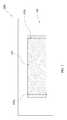
- FIG. 1illustrates a silicon substrate
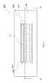
- FIG. 2shows a top view of a trench having two slanted side walls made on the silicon substrate in accordance with an embodiment.
- FIG. 3shows a top view of a polymer layer formed in the trench in accordance with an embodiment.
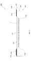
- FIG. 4illustrates a top view of an array of polymer waveguides fabricated in the silicon trench in accordance with an embodiment.
- FIG. 5illustrates a cross sectional view of a polymer waveguides in the silicon trench along a line AA′ in FIG. 4 in accordance with an embodiment.
- FIG. 6shows a cross sectional view after making contact lines for active device on the silicon substrate in accordance with an embodiment.
- FIG. 7illustrates adding solder bumps and active devices on the silicon substrate in accordance with an embodiment.
- FIG. 8is a schematic diagram of a flow chart illustrating a method for fabricating the optical interconnect module in accordance with an embodiment.
- FIG. 9shows an examplenary optical module having a polymer waveguide interconnected with a transmitter and a receiver from the same surface of a silicon substrate in accordance with the disclosed embodiment.
- FIG. 10illustrates a schematic diagram of the interconnect module disclosed in FIG. 9 which has been reduced to practice, in accordance with the disclosed embodiment.
- the terms “above”, “over”, “to”, “between”, and “on” as used hereinmay refer to a relative position of one layer with respect to other layers.
- One layer “above”, “over”, or “on” another layer or bonded “to” or in “contact” with another layermay be directly in contact with the other layer or may have one or more intervening layers.
- One layer “between” layersmay be directly in contact with the layers or may have one or more intervening layers.
- Optical interconnectis a means of communication by optical modules.
- Optical communication systemsoften apply a vertical-cavity surface-emitting laser VCSEL for convenient configurations and easy assembling.
- the vertical-cavity surface-emitting laser, or VCSELis a type of semiconductor laser diode with laser beam emission perpendicular from the top surface, contrary to conventional edge-emitting semiconductor lasers (also in-plane lasers) which emit from surfaces formed by cleaving the individual chip out of a wafer.
- Vertical cavity self-emitting laser or VCSEL laser emitting light at wavelengths from 650 nm to 1300 nmare typically based on gallium arsenide (GaAs) wafers with diffraction Bragg reflectors (DBRs) formed from GaAs and aluminum gallium arsenide (Al x Ga (1-x) As).
- GaAsgallium arsenide
- DBRsdiffraction Bragg reflectors
- VCSELsion-implanted VCSELs and Oxide VCSELs.
- An additional adhesive layersuch as a non-conductive film (NCF) may also be applied to enhance adhesion of the components to the silicon substrate.
- the adhesive layercan be made from an organic film such as polyimide.
- the high speed conductive linesincluding an RF transmission devices, are designed on the same surface as the polymer waveguides to connect the driver IC and VCSEL arrays as well as to connect trans-impedance amplifier (TIA) arrays.
- TIAtrans-impedance amplifier
- a VCSEL arrayhas four VCSEL lasers packed in a row.
- the data rate of the optical enginecan be operated at 25 Giga-bits per second (Gbps) per channel, and can be extended to higher data rates such as 50 Gbps per channel.
- GbpsGiga-bits per second
- VCSEL applicationsinclude fiber optic communications, precision sensing, computer mice and laser printers.
- the optical interconnects and platforms in accordance with embodimentsmay be assembled without the optical lenses and fiber ribbons commonly utilized in conventional optical interconnect assemblies. Assembly time can be reduced compared to conventional techniques through use of semiconductor process technologies for the formation of conductive transmission lines and flip chip integration of the active optical devices such as the driver IC chip, lasers, PD, and receiver (e.g. TIA) chips.
- the fabrication techniquesmay allow for improved RF performance of the electrical signals and increased data rates of the optical interconnects.
- the embodiments illustrated belowmay be integrated as a PCB-based optical interconnect.
- the embodimentmay be utilized to improve optical coupling with the VCSEL/PD by monolithically integrating a silicon wafer interposer with a VCSEL laser within a packaging platform like PCB, and a polymer waveguide.
- substrate 100has a silicon surface 140 .
- the thickness of the silicon substrate 140is chosen to be thin so it is light and yet has enough strength to support photonics elements on the top surface during its fabrication process and in its long term operation. Typically the thickness is in the range of 50 microns to 2 millimeters.
- FIG. 2shows a top view of a trench, which has two opposite slanted side walls formed on the top surface of the silicon substrate in accordance with an embodiment.
- the trench 130has an elongated shape, likely a rectangular.
- the length of the trench 130accommodates the length of the polymer waveguides.
- the width of the trench 130allows the full array of waveguides to be packed inside the trench.
- the depth of the trench 130allows to accommodate at least the full package of the polymer waveguides. This depth can vary from a few microns to one millimeter.
- the opposite side walls 120 a and 120 bare built as slanted slopes upon which the ends of the polymer waveguides lie.
- the slanted anglesshould be close to but are not exactly 45 degrees in order to easy align with the light source and optical receiver.
- the two slanted angles of the two side wallsdon't have to be equal either.
- a number of patterning techniquescan be used. Photolithography commonly applied in CMOS process technology provides various ways in controlling the lithography exposure energy to achieve smooth and accurate slant slopes. For example, a moving exposure shutter or a shrinking window during photo-exposure or a variable scanner light intensity during exposure are available techniques. Reflector angle control tolerance and surface smoothness are critical to optical energy efficiency, therefore fabrication in this step should have appropriate requirements.
- FIG. 3shows a top view 300 of a polymer layer 135 formed in the trench 130 in accordance with an embodiment. It is another preparation step to form an optical passive path, i.e. the polymer waveguides, inside the trench.
- an optical passive pathi.e. the polymer waveguides
- this applicationdiscloses a polymer waveguide fabricated directly on the silicon substrate. As an integrated part of the substrate, the polymer waveguide enables low optical coupling loss at interfaces and stable alignment along the optical path. Meanwhile, fabrication cost from attaching waveguides to an interposer is much reduced.
- the polymer layer 135is formed in the trench which typically includes a polymer cladding layer having a thickness in the range of one to 50 microns and a polymer core layer on the polymer cladding layer.
- the polymer corehas a thickness ranging from a few microns for single mode light to hundreds of microns for multi-mode waveguides. It is also possible to deposit only one layer of polymer as the core without a special cladding layer surrounding the core. However thus produced polymer waveguide may not be optically efficient.
- Polymersinclude PMMA, polyimide, and other optical quality polymer materials. It typically includes two polymer materials for core and for cladding which have distinguishable refractive indices at the working wavelengths.
- Claddinggenerally is made of silicone (index ⁇ 1.46), core made of PMMA or polyimide which has index in range of 1.49 and 1.59.
- the slanted trench side walls 120 a and 120 bare covered at least partially by both the cladding and the core layers.
- FIG. 4illustrates a top view of an array of polymer waveguides fabricated in the silicon trench in accordance with an embodiment.
- the polymer layeris patterned into strip shaped parallel polymer waveguides 122 sitting in the trench of the silicon substrate 140 .
- Each waveguide 122has two ends resting on the slanted side walls 120 a and 120 b , thus forming slanted interfaces 125 a and 125 b .
- the resultant slanted interfacesmust meet high optical quality requirements such as good high frequency roughness and low light scattering. Patterning techniques include lithography and laser writing.
- a different polymer materialshould be deposited below the core polymer layer and also deposited on and around the core waveguides after patterning the waveguides so each of the waveguides 122 is surrounded by the cladding polymer layers.
- Each polymer striphas width around 4-6 microns for a single mode waveguide, or in a range of 10 to hundreds of microns for a multi-mode waveguide. This patterning step is performed using lithography technique and selective etch so the polymer is removed but the underlining silicon is intact.
- FIG. 5illustrates a cross sectional view of an array of polymer waveguides in the silicon trench along a line AA′ in FIG. 4 in accordance with an embodiment.
- diagram 500has a silicon substrate 140 , a bottom surface 160 and a top surface 170 where the optical interconnector is built.
- the silicon trench 130opens a space for disposing the polymer waveguides 122 .
- Each of the waveguides 122has two end reflective surfaces 125 a and 125 b interfacing the two slanted side walls 120 a and 120 b of the silicon trench 130 .
- a polymer cladding material(not shown) is typically disposed wrapping around the waveguide 122 on its bottom surface, top surface, side walls, and the slanted interfaces in order to have uniformly matched refractive index difference.
- Each of the waveguides in FIG. 5has a straight portion 124 and two slanted ends 125 a and 125 b .
- the slanted angleis made into 45 degrees for easy alignment, but it can be formed different than 45 degrees and the two slanted ends may have different angles.
- both ends 125 a and 125 bare referred to as 45 degree reflectors in this description.
- the waveguide endsserve like 45 degree bending mirrors.
- the passivating layershould have a refractive index lower than that of the polymer core to guarantee total light internal reflection.
- FIG. 6shows a cross sectional view after making contact lines on the silicon substrate in accordance with an embodiment.
- Conductive linesare formed on the left of the trench for optical input and on the right for optic output on the silicon top surface in FIG. 6 .
- siliconis a semiconductor
- an insulating film 129 chas to be deposited first before any electronic devices are laid down.
- the insulating film 129 cis either deposited or grown on the silicon surface 170 outside the trench 130 .
- the surface 170is a platform to carry interconnects for active optical devices, such as laser diodes in a transmitter or photodetectors in a receiver, IC drivers, amplifiers, and other electronic devices.
- Polymer waveguides in the trenchare located on the same side of the substrate, so there will be no device disposed on the other side 160 of the silicon substrate.
- the waveguidesare fabricated together with interconnecting the optical devices, there will be no bonding step to integrate a separate waveguide. Because there is not a substrate flip-over step to change the working surface when a holder stage holds the work piece during fabrication, therefore fabrication is more straightforward and there is less risk to damage the devices from stage changing sides.
- contact lines 110 xare patterned on the insulation layer 129 c on the top silicon surface 170 .
- transmission linesare not all drawn or labeled.
- Metalslike copper, aluminum, tungsten, titanium, or alloys can be chosen for high speed transmission lines.
- Metal layer deposition techniques known in the semiconductor industrycan be applied. These deposition techniques include, but not limited to, sputtering of metal, followed by wet/dry etch, metal plating, or laser writing.
- line forming techniquescan also be applied, for example, first form trenches into the top surface of the insulating layer; second, deposit a metal layer on the trenches, followed by a planarization technique like chemical mechanical polishing (CMP) or selective dry/wet etching to remove the excess metal from areas outside the trenches.
- CMPchemical mechanical polishing
- formation of the electrical traces 110 x on the substratemay lead to improved RF signal performance from the high dielectric constant of the silicon material, typically ranging in 3 to 4 for infrared light.
- the resultant data rate of the optical devicegoes up to 25 Giga-bits per second (Gbps) per channel, and can be extended to even higher data rates such as 50 Gbps per channel.
- FIG. 7illustrates positioning bonding pillars on conducting lines and connecting the solder bumps to active photonic devices on the silicon substrate in accordance with an embodiment.
- a diagram 700illustrates that proper bonding pillars 141 x , made by solder bumps, are formed on the transmission lines as contacting spots for connecting to active optical devices and IC drivers or other electronics. Again not all bonding pillars are shown as 141 x in FIG. 7 .
- Active optical devices in the input sidesuch as vertical cavity surface emission laser (VCSEL) 121 , laser driver 121 A, and active optical devices in the output side such as photodiode (PD) 127 , receiver driver 127 A, trans-impedance amplifier (TIA not shown in the figure), RF circuits (not shown in FIG. 7 ), and other electronic devices are attached to transmission lines 110 x engraved as metal-in-insulator structures on the top surface of the silicon substrate.
- Other optoelectronic devicesmaybe assembled on a PCB unit 150 packaged to the silicon surface. As stated above, direct patterned transmission lines on the surface enables high speed performance.
- a room temperature adhesion filmsuch as one made of polyimide maybe deposited over the transmission lines 110 x and interconnecting pillars/bumps 141 x to insulate them from the above active devices, leaving only the contact spots to the active devices unblocked.
- Another way to insulateis to apply a thermally curable or UV curable non-conductive film (NCF) over the top surface followed by heating or UV shining to enhance adhesion of the parts.
- NCFthermally curable or UV curable non-conductive film
- a cleaning processis also applied to ensure the bonding pillars 141 x properly connect to the active devices.
- the adhesion film or NCFis not shown in FIG. 7 .
- the above described optoelectronics assembly including the interconnectionsforms an optical engine.
- the optical engineis assembled to external circuits packaged through bond pads on a PCB 150 .
- the optical engineis assembled with a flexible printed circuit board (FCB).
- FCBflexible printed circuit board
- the optical engineis assembled within a periphery of an opening in the PCB. While not separately illustrated, such a configuration is compatible with other embodiments, including that described with regard to FIG. 7 .
- VCSEL laser output beamis aligned to match the first 45 degree reflector 125 a along path 723 a , the beam changes trajectory 90 degree by the reflector 125 a which couples light beam to the straight portion of waveguides 122 .
- Lightis reflected the second time by the second 45 degree reflector 125 b which is aligned to photodetector 127 , changes trajectory again, travels along 723 b back into photodetector 127 , thus completing the full optical path as shown in FIG. 7 .
- the completed optical interconnect systemrests on the silicon substrate 140 which provides a mechanical support structure for a PCB or FCB 150 on which other bonding pads and external form factors may reside. Without the silicon substrate as an interposer, it may be too fragile to depend on PCB film to hold the photonic devices and the arrays of waveguides during manufacturing and in long term operation.
- Another embodimentincludes attaching a metal plate to the silicon substrate to strengthen the interposer.
- the metal plateis made of some compatible materials such as stainless steel.
- Anisotropic conductive filmhas been widely used in for higher signal densities and smaller overall packages, ideal for optoelectronic end products.
- the anisotropic materialfor example, a thermosetting resin containing conductive particles
- the anisotropic materialis first deposited on the PCB using a lamination process.
- the optical engine on the silicon substrateis then placed in position over the PCB and the two sides are pressed together to mount the optical engine to the PCB board.
- this mounting processis done with no heat or a minimal amount of heat that is just sufficient to cause the anisotropic material to become slightly tacky.
- the particlesare trapped between the PCB and the optoelectronics elements, thereby creating an electrical connection there between.
- thermosetting resinIn other locations where it is not terminated with electrodes, particles are insulated by the thermosetting resin.
- the amount of thermal energy requiredis higher due to the need to first flow the adhesive and allow the two sides to come together into electrical contact, and then to cure the adhesive and create a lasting reliable bond.
- the temperatures, times, and pressure required for these processesmust be controlled properly.
- FIG. 8is a schematic diagram of a flow chart 800 illustrating a method for fabricating the optical interconnect module with polymer waveguide in a silicon substrate in accordance with an embodiment.
- the fabrication sequencemay include the first step 802 : provide a silicon substrate having a top silicon surface for both polymer waveguides and active input and output devices, and a bottom silicon surface as a support holder. A trench is made on the top silicon surface for positioning the waveguides.
- step 804pattern the first and second sidewalls of the trench to be reflective slanted surfaces.
- the slanted first and second sidewallsare opposite to each other.
- the slanted angles of the first and second sidewallsform a desired optical path, it is exemplary 45 degrees for both but they are not necessarily the same and they don't have to be 45 degrees.
- a number of ways in controlling the lithography exposure energycan be applied to achieve smooth and accurate slant slopes.
- a moving exposure shutter or a shrinking window during photo-exposure or a variable scanner light intensity during exposureare available techniques.
- Reflector angle control tolerance and surface smoothnessare critical to optical path efficiency, therefore fabrication of this step should have appropriate speciation requirements.
- Advanced micro patterning technologycan provide such capability today.
- step 806deposit a polymer layer in the trench, covering part of the slanted slopes. If a core polymer layer and a cladding polymer layer are desired, first deposit the cladding polymer at the bottom of the trench and the slanted slope, then cover the cladding polymer layer with the core polymer layer.
- step 808pattern polymer core layer into multiple waveguides each having 45 degree end reflectors, deposit a second polymer cladding layer on the polymer waveguides.
- the width of each waveguidecan be from 5 microns for a single mode waveguide to a large one up to 500 microns for a multi-mode waveguide.
- step 810deposit an insulating layer on silicon surface outside the trench to form base for photonic device interconnections.
- step 812pattern transmission lines in the insulating layer.
- One way to form transmission linesis to pattern trenches on insulating layer and fill in metal to form transmission lines, or another way is to deposit metal layer and pattern it into lines with etching or Laser writing is also a way to get lines formed.
- the metal layermay be aluminum, tungsten, stainless steel, etc. If it is copper, process will need to follow copper plating techniques.
- step 814grow bonding pillars, for example, as solder bumps for flip chip mounting with bond pads.
- step 816assemble active optical devices (VCSEL/PD) with transmission lines via interconnecting pillars/solder bumps.
- VCSEL/PDactive optical devices
- FIG. 9shows an examplenary optical module having an array of polymer waveguides interconnected with a transmitter including a VCSEL laser on the left side of the waveguides, and a receiver including a photodetector on the right side of the waveguides, on the same surface of a silicon substrate in accordance with the disclosed embodiment.
- FIG. 10illustrates a schematic diagram of the interconnect module disclosed in FIG. 9 , which has been reduced to practice, in accordance with the disclosed embodiment.
- embodimentsare not limited to this particular sequence, and alternative fabrication sequences are envisioned.
Landscapes
- Physics & Mathematics (AREA)
- General Physics & Mathematics (AREA)
- Optics & Photonics (AREA)
- Engineering & Computer Science (AREA)
- Microelectronics & Electronic Packaging (AREA)
- Electromagnetism (AREA)
- Computer Networks & Wireless Communication (AREA)
- Signal Processing (AREA)
- Condensed Matter Physics & Semiconductors (AREA)
- Chemical & Material Sciences (AREA)
- Crystallography & Structural Chemistry (AREA)
- Optical Couplings Of Light Guides (AREA)
- Optical Integrated Circuits (AREA)
- Ceramic Engineering (AREA)
- Inorganic Chemistry (AREA)
- Computer Hardware Design (AREA)
- Power Engineering (AREA)
- Semiconductor Lasers (AREA)
- Light Receiving Elements (AREA)
Abstract
Description
- This application claims the benefit of U.S. Provisional Patent Applications No. 62/508,940, titled “OPTICAL COUPLING STRUCTURE” filed on May 19, 2017, and No. 62/509,892, titled “OPTICAL INTERCONNECT MODULES” filed on May 23, 2017, which are incorporated by reference herein in their entirety.
- Embodiments described herein relate to optical interconnect modules, and more particularly optical sub-assembly systems in optical interconnects.
- Cloud computing, enterprise networks, and data center networks continue to drive increased bandwidth demand of optical waveguides for metro and long haul wires, and also rack-to-rack wires within data centers to 100 Gbps and beyond. Increased bandwidth demand has motivated overall high data transmission speed on entire optical systems.
- Optical interconnect techniques continue to gain attention as potential solutions for high-speed data transmission between systems, and over a variety of distances. For example, optical interconnect solutions have been proposed for a number of applications, such as between racks in a data center, between household consumer electronics, and between boards or chips within server systems. Optical interconnects are particularly suitable for adoption within transmitter and receiver systems.
- In a conventional optical sub-assembly (OSA) design, a transmitter module includes a transmission laser, a driver integrated circuit (IC), and a printed circuit board (PCB), while a receiver module includes a photodetector (PD), a trans-impedance amplifier (TIA), and a PCB. The optical path between the transmission laser (commonly a vertical cavity surface emitting laser (VCSEL)) and PD is typically an optical fiber, such as a fiber ribbon and optical waveguides. Complex beam routers including a focusing lens, a prism, and a fiber connector are used to precisely align the optical fiber with the optical path. Mechanical structures including screws, clips, alignment pins and structural housing are commonly used to secure and align the beam routers.
- However, an optical interconnect typically requires coupling of fiber assembly and lasers which involves an external lens alignment, adding complexity and energy loss. A less complicated assembly technique is needed to improve efficiency and reduce cost.
- The application discloses a silicon substrate based optical interconnect module which includes a trench, having a first and a second slanted side walls opposite to each other, a number of polymer waveguides formed in the trench, each waveguide includes a straight portion and two end reflectors formed on the slanted side walls of the trench, a light source and an optical receiver disposed on an insulated layer on the silicon surface outside the trench. The polymer waveguides are employed to connect the optical signal between the light source and the receiving devices. Conductive lines are patterned on the insulating layer and connect to the light source and the optical receiver. The light source and the optical receiver are aligned respectively to the two end reflectors of each polymer waveguide such that an optical path is formed from the light source device through the plurality of polymer waveguides to the optical receiver device, via reflection by the two end reflectors.
- Optionally, the polymer waveguides include a polymer cladding layer disposed on the trench's bottom covering the first and second slanted side walls, and a polymer core layer disposed on the polymer cladding layer, wherein a refractive index of the polymer cladding layer is lower than a refractive index of the polymer core layer such that total internal reflection occurs when light travels inside the polymer waveguides.
- Optionally, the first slanted side wall of the trench has a slanted angle approximately set at 45 degrees to align optically to the light source device.
- Optionally, the second slanted side wall of the trench has a slanted angle approximately set at 45 degrees to align optically to the optical receiver device.
- Optionally, the light source device comprises a vertical cavity surface emission laser (VCSEL), or a vertical cavity surface emission laser array (VCSELs) emitting infrared light. Optionally, the optical receiver device is a photodiode (PD) or a photodiode array (PDs).
- Optionally, the silicon substrate has a thickness ranging from 50 microns to 2 mm.
- Optionally, the light source device and the optical receiver device are respectively connected to the plurality of conductive lines by solder bumps.
- Optionally, the conductive lines are made of one of tungsten (W), aluminum (Al), copper (Cu), gold (Au), silver (Ag), stainless steel, or an alloy.
- Optionally, the conductive lines are high speed RF transmission lines capable of operating at 25 Gbps per channel.
- The application also discloses a method of fabricating an optical interconnect apparatus according to one embodiment. The method comprises: providing a silicon substrate having a top silicon surface; forming a trench on the top silicon surface; patterning a first and a second slanted side walls of the trench, wherein the first and second slanted sidewalls are opposite to each other; forming a plurality of polymer waveguides in the trench by depositing a first polymer cladding layer in the trench covering the first and second slanted side walls, followed by depositing a polymer core layer on the first polymer cladding layer, patterning the polymer core layer and covering the patterned polymer core layer with a second polymer cladding layer, wherein the plurality of polymer waveguides each has one straight portion and two slanted end reflectors; depositing an insulating layer on the silicon top surface outside the trench; patterning conductive lines in the insulating layer; growing solder bumps on conductive lines for flip chip mounting with bond pads; connecting a light source device with one of the conductive lines near the first slanted side wall of the trench and an optical receiver device with another one of the conductive lines near the second slanted side wall of the trench; and aligning the light source device and the optical receiver device with the slanted end reflectors of the plurality of polymer waveguides.
- Optionally, the light source device comprises a vertical cavity surface emitting laser (VCSEL) and wherein the optical receiver device comprises a photodetector (PD).
- Optionally, the patterning the first and second slanted side walls of the trench comprises applying a variable lithography exposure energy to achieve smooth and accurate slanted angles.
- Optionally, the slanted end reflectors have approximately 45 degree slanted angles.
- Optionally, patterning the conductive lines comprises forming trenches and filling in metal in the trenches, followed by removing excess metal by polishing (CMP) or by selective etch to clean up metal outside the trenches.
- Optionally, patterning the conductive lines comprises depositing a metal layer, patterning the metal layer into lines by selective etch, or laser writing.
- Optionally, the metal layer may be aluminum, tungsten, etc. If it is copper, process will need to apply copper plating techniques.
- Having thus described some embodiments in general terms, reference will now be made to the accompanying drawings, which are not necessarily drawn to scale.
FIG. 1 illustrates a silicon substrate.FIG. 2 shows a top view of a trench having two slanted side walls made on the silicon substrate in accordance with an embodiment.FIG. 3 shows a top view of a polymer layer formed in the trench in accordance with an embodiment.FIG. 4 illustrates a top view of an array of polymer waveguides fabricated in the silicon trench in accordance with an embodiment.FIG. 5 illustrates a cross sectional view of a polymer waveguides in the silicon trench along a line AA′ inFIG. 4 in accordance with an embodiment.FIG. 6 shows a cross sectional view after making contact lines for active device on the silicon substrate in accordance with an embodiment.FIG. 7 illustrates adding solder bumps and active devices on the silicon substrate in accordance with an embodiment.FIG. 8 is a schematic diagram of a flow chart illustrating a method for fabricating the optical interconnect module in accordance with an embodiment.FIG. 9 shows an examplenary optical module having a polymer waveguide interconnected with a transmitter and a receiver from the same surface of a silicon substrate in accordance with the disclosed embodiment.FIG. 10 illustrates a schematic diagram of the interconnect module disclosed inFIG. 9 which has been reduced to practice, in accordance with the disclosed embodiment.- The present disclosure is further described below in combination with the drawings and embodiments. It should be understood that, the specific embodiments described herein are merely used to explain the present disclosure rather than limiting the present disclosure. In addition, it should be stated that, in order to facilitate the description, merely a part of structures related to the present disclosure rather than the whole structure are illustrated in the drawings.
- In various embodiments, description is made with reference to figures. However, certain embodiments may be practiced without one or more of these specific details, or in combination with other known methods and configurations. In the following description, numerous specific details are set forth, such as specific configurations, dimensions and processes, etc., in order to provide a thorough understanding of the embodiments. In other instances, well-known semiconductor processes and manufacturing techniques have not been described in particular detail in order to not unnecessarily obscure the embodiments. Reference throughout this specification to “one embodiment” means that a particular feature, structure, configuration, or characteristic described in connection with the embodiment is included in at least one embodiment. Thus, the appearances of the phrase “in one embodiment” in various places throughout this specification are not necessarily referring to the same embodiment. Furthermore, the particular features, structures, configurations, or characteristics may be combined in any suitable manner in one or more embodiments.
- The terms “above”, “over”, “to”, “between”, and “on” as used herein may refer to a relative position of one layer with respect to other layers. One layer “above”, “over”, or “on” another layer or bonded “to” or in “contact” with another layer may be directly in contact with the other layer or may have one or more intervening layers. One layer “between” layers may be directly in contact with the layers or may have one or more intervening layers.
- It needs to be noted that, specific details are illustrated in the description below for fully understanding the disclosure. However, the disclosure can be implemented in other ways different from those described herein, and it may be similarly generalized by one skilled in the art without departing from the concept of the disclosure. Therefore, the disclosure will not be limited to the specific embodiments disclosed below.
- Optical interconnect is a means of communication by optical modules. Optical communication systems often apply a vertical-cavity surface-emitting laser VCSEL for convenient configurations and easy assembling.
- The vertical-cavity surface-emitting laser, or VCSEL is a type of semiconductor laser diode with laser beam emission perpendicular from the top surface, contrary to conventional edge-emitting semiconductor lasers (also in-plane lasers) which emit from surfaces formed by cleaving the individual chip out of a wafer. Vertical cavity self-emitting laser or VCSEL laser emitting light at wavelengths from 650 nm to 1300 nm are typically based on gallium arsenide (GaAs) wafers with diffraction Bragg reflectors (DBRs) formed from GaAs and aluminum gallium arsenide (AlxGa(1-x)As).
- There are now two main methods of restricting the current in a VCSEL characterized by two types of VCSELs: ion-implanted VCSELs and Oxide VCSELs. An additional adhesive layer, such as a non-conductive film (NCF), may also be applied to enhance adhesion of the components to the silicon substrate. The adhesive layer can be made from an organic film such as polyimide. The high speed conductive lines, including an RF transmission devices, are designed on the same surface as the polymer waveguides to connect the driver IC and VCSEL arrays as well as to connect trans-impedance amplifier (TIA) arrays. Typically a VCSEL array has four VCSEL lasers packed in a row.
- In accordance with an embodiment, the data rate of the optical engine can be operated at 25 Giga-bits per second (Gbps) per channel, and can be extended to higher data rates such as 50 Gbps per channel. VCSEL applications include fiber optic communications, precision sensing, computer mice and laser printers.
- Embodiments disclosed below describe optical interconnects and application platforms. In one aspect, the optical interconnects and platforms in accordance with embodiments may be assembled without the optical lenses and fiber ribbons commonly utilized in conventional optical interconnect assemblies. Assembly time can be reduced compared to conventional techniques through use of semiconductor process technologies for the formation of conductive transmission lines and flip chip integration of the active optical devices such as the driver IC chip, lasers, PD, and receiver (e.g. TIA) chips. In addition, the fabrication techniques may allow for improved RF performance of the electrical signals and increased data rates of the optical interconnects. The embodiments illustrated below may be integrated as a PCB-based optical interconnect. In particular, the embodiment may be utilized to improve optical coupling with the VCSEL/PD by monolithically integrating a silicon wafer interposer with a VCSEL laser within a packaging platform like PCB, and a polymer waveguide.
- As shown in
FIG. 1 ,substrate 100 has asilicon surface 140. The thickness of thesilicon substrate 140 is chosen to be thin so it is light and yet has enough strength to support photonics elements on the top surface during its fabrication process and in its long term operation. Typically the thickness is in the range of 50 microns to 2 millimeters. FIG. 2 shows a top view of a trench, which has two opposite slanted side walls formed on the top surface of the silicon substrate in accordance with an embodiment. Thetrench 130 has an elongated shape, likely a rectangular. The length of thetrench 130 accommodates the length of the polymer waveguides. The width of thetrench 130 allows the full array of waveguides to be packed inside the trench. The depth of thetrench 130 allows to accommodate at least the full package of the polymer waveguides. This depth can vary from a few microns to one millimeter. Theopposite side walls FIG. 3 shows atop view 300 of apolymer layer 135 formed in thetrench 130 in accordance with an embodiment. It is another preparation step to form an optical passive path, i.e. the polymer waveguides, inside the trench. Although in many optical interconnect modules, a waveguide may be formed separately first and attached to one surface of a substrate later, using an adhesive layer, this application discloses a polymer waveguide fabricated directly on the silicon substrate. As an integrated part of the substrate, the polymer waveguide enables low optical coupling loss at interfaces and stable alignment along the optical path. Meanwhile, fabrication cost from attaching waveguides to an interposer is much reduced. Thepolymer layer 135 is formed in the trench which typically includes a polymer cladding layer having a thickness in the range of one to 50 microns and a polymer core layer on the polymer cladding layer. The polymer core has a thickness ranging from a few microns for single mode light to hundreds of microns for multi-mode waveguides. It is also possible to deposit only one layer of polymer as the core without a special cladding layer surrounding the core. However thus produced polymer waveguide may not be optically efficient. Polymers include PMMA, polyimide, and other optical quality polymer materials. It typically includes two polymer materials for core and for cladding which have distinguishable refractive indices at the working wavelengths. Cladding generally is made of silicone (index ˜1.46), core made of PMMA or polyimide which has index in range of 1.49 and 1.59. The slantedtrench side walls FIG. 4 illustrates a top view of an array of polymer waveguides fabricated in the silicon trench in accordance with an embodiment. As shown in the diagram400 inFIG. 4 , the polymer layer is patterned into strip shapedparallel polymer waveguides 122 sitting in the trench of thesilicon substrate 140. Eachwaveguide 122 has two ends resting on the slantedside walls slanted interfaces waveguides 122 is surrounded by the cladding polymer layers. Each polymer strip has width around 4-6 microns for a single mode waveguide, or in a range of 10 to hundreds of microns for a multi-mode waveguide. This patterning step is performed using lithography technique and selective etch so the polymer is removed but the underlining silicon is intact.FIG. 5 illustrates a cross sectional view of an array of polymer waveguides in the silicon trench along a line AA′ inFIG. 4 in accordance with an embodiment.- As shown in
FIG. 5 , diagram500 has asilicon substrate 140, abottom surface 160 and atop surface 170 where the optical interconnector is built. Thesilicon trench 130 opens a space for disposing thepolymer waveguides 122. Each of thewaveguides 122 has two endreflective surfaces side walls silicon trench 130. A polymer cladding material (not shown) is typically disposed wrapping around thewaveguide 122 on its bottom surface, top surface, side walls, and the slanted interfaces in order to have uniformly matched refractive index difference. - Each of the waveguides in
FIG. 5 has astraight portion 124 and two slanted ends125aand125b. Often the slanted angle is made into 45 degrees for easy alignment, but it can be formed different than 45 degrees and the two slanted ends may have different angles. As an exemplary embodiment, both ends125aand125bare referred to as 45 degree reflectors in this description. The waveguide ends serve like 45 degree bending mirrors. Light comes from an input device above theslanted end 125aat one side of the trench gets reflected 90 degrees into thehorizontal portion 124, light then travels through the waveguide by total internal reflection, hits thesecond end interface 125b, gets reflected off by the second 45 degree reflector, changes trajectory up and returns back to the output receiver device over the other side of the trench. - If no designated cladding layer is included in the polymer waveguide, it is recommended to seal the waveguide hermetically with a stable material to protect the waveguides. The passivating layer should have a refractive index lower than that of the polymer core to guarantee total light internal reflection.
FIG. 6 shows a cross sectional view after making contact lines on the silicon substrate in accordance with an embodiment. Conductive lines are formed on the left of the trench for optical input and on the right for optic output on the silicon top surface inFIG. 6 . Because silicon is a semiconductor, an insulatingfilm 129chas to be deposited first before any electronic devices are laid down. The insulatingfilm 129cis either deposited or grown on thesilicon surface 170 outside thetrench 130. Thesurface 170 is a platform to carry interconnects for active optical devices, such as laser diodes in a transmitter or photodetectors in a receiver, IC drivers, amplifiers, and other electronic devices. Polymer waveguides in the trench are located on the same side of the substrate, so there will be no device disposed on theother side 160 of the silicon substrate. The waveguides are fabricated together with interconnecting the optical devices, there will be no bonding step to integrate a separate waveguide. Because there is not a substrate flip-over step to change the working surface when a holder stage holds the work piece during fabrication, therefore fabrication is more straightforward and there is less risk to damage the devices from stage changing sides.- As shown in
FIG. 6 , first,contact lines 110x(various transmission lines) are patterned on theinsulation layer 129con thetop silicon surface 170. Please note that inFIG. 6 , transmission lines are not all drawn or labeled. Metals like copper, aluminum, tungsten, titanium, or alloys can be chosen for high speed transmission lines. Metal layer deposition techniques known in the semiconductor industry can be applied. These deposition techniques include, but not limited to, sputtering of metal, followed by wet/dry etch, metal plating, or laser writing. Other line forming techniques can also be applied, for example, first form trenches into the top surface of the insulating layer; second, deposit a metal layer on the trenches, followed by a planarization technique like chemical mechanical polishing (CMP) or selective dry/wet etching to remove the excess metal from areas outside the trenches. - In accordance with the embodiments, formation of the
electrical traces 110xon the substrate may lead to improved RF signal performance from the high dielectric constant of the silicon material, typically ranging in 3 to 4 for infrared light. The resultant data rate of the optical device goes up to 25 Giga-bits per second (Gbps) per channel, and can be extended to even higher data rates such as 50 Gbps per channel. FIG. 7 illustrates positioning bonding pillars on conducting lines and connecting the solder bumps to active photonic devices on the silicon substrate in accordance with an embodiment. Shown inFIG. 7 a diagram700 illustrates thatproper bonding pillars 141x, made by solder bumps, are formed on the transmission lines as contacting spots for connecting to active optical devices and IC drivers or other electronics. Again not all bonding pillars are shown as141xinFIG. 7 .- Active optical devices in the input side such as vertical cavity surface emission laser (VCSEL)121,
laser driver 121A, and active optical devices in the output side such as photodiode (PD)127,receiver driver 127A, trans-impedance amplifier (TIA not shown in the figure), RF circuits (not shown inFIG. 7 ), and other electronic devices are attached totransmission lines 110xengraved as metal-in-insulator structures on the top surface of the silicon substrate. Other optoelectronic devices maybe assembled on aPCB unit 150 packaged to the silicon surface. As stated above, direct patterned transmission lines on the surface enables high speed performance. - An insulation is necessary between the active devices and the conductive lines except at locations the pillars/bumps connect to the active devices. A room temperature adhesion film such as one made of polyimide maybe deposited over the
transmission lines 110xand interconnecting pillars/bumps 141xto insulate them from the above active devices, leaving only the contact spots to the active devices unblocked. Another way to insulate is to apply a thermally curable or UV curable non-conductive film (NCF) over the top surface followed by heating or UV shining to enhance adhesion of the parts. A cleaning process is also applied to ensure thebonding pillars 141xproperly connect to the active devices. The adhesion film or NCF is not shown inFIG. 7 . - The above described optoelectronics assembly including the interconnections forms an optical engine. The optical engine is assembled to external circuits packaged through bond pads on a
PCB 150. In some cases, the optical engine is assembled with a flexible printed circuit board (FCB). In an embodiment, the optical engine is assembled within a periphery of an opening in the PCB. While not separately illustrated, such a configuration is compatible with other embodiments, including that described with regard toFIG. 7 . - In
FIG. 7 , VCSEL laser output beam is aligned to match the first 45degree reflector 125aalongpath 723a, the beam changes trajectory 90 degree by thereflector 125awhich couples light beam to the straight portion ofwaveguides 122. Light is reflected the second time by the second 45degree reflector 125bwhich is aligned tophotodetector 127, changes trajectory again, travels along723bback intophotodetector 127, thus completing the full optical path as shown inFIG. 7 . - The completed optical interconnect system rests on the
silicon substrate 140 which provides a mechanical support structure for a PCB orFCB 150 on which other bonding pads and external form factors may reside. Without the silicon substrate as an interposer, it may be too fragile to depend on PCB film to hold the photonic devices and the arrays of waveguides during manufacturing and in long term operation. - Another embodiment includes attaching a metal plate to the silicon substrate to strengthen the interposer. The metal plate is made of some compatible materials such as stainless steel.
- Anisotropic conductive film (ACF) has been widely used in for higher signal densities and smaller overall packages, ideal for optoelectronic end products. In this process, the anisotropic material, for example, a thermosetting resin containing conductive particles, is first deposited on the PCB using a lamination process. The optical engine on the silicon substrate is then placed in position over the PCB and the two sides are pressed together to mount the optical engine to the PCB board. In many cases this mounting process is done with no heat or a minimal amount of heat that is just sufficient to cause the anisotropic material to become slightly tacky. In using a thermosetting resin containing conductive particles, the particles are trapped between the PCB and the optoelectronics elements, thereby creating an electrical connection there between. In other locations where it is not terminated with electrodes, particles are insulated by the thermosetting resin. For bonding, the amount of thermal energy required is higher due to the need to first flow the adhesive and allow the two sides to come together into electrical contact, and then to cure the adhesive and create a lasting reliable bond. The temperatures, times, and pressure required for these processes must be controlled properly.
FIG. 8 is a schematic diagram of aflow chart 800 illustrating a method for fabricating the optical interconnect module with polymer waveguide in a silicon substrate in accordance with an embodiment.- The fabrication sequence may include the first step802: provide a silicon substrate having a top silicon surface for both polymer waveguides and active input and output devices, and a bottom silicon surface as a support holder. A trench is made on the top silicon surface for positioning the waveguides. In
step 804, pattern the first and second sidewalls of the trench to be reflective slanted surfaces. The slanted first and second sidewalls are opposite to each other. The slanted angles of the first and second sidewalls form a desired optical path, it is exemplary 45 degrees for both but they are not necessarily the same and they don't have to be 45 degrees. - To make the elongated trench and the slanted side walls, a number of ways in controlling the lithography exposure energy can be applied to achieve smooth and accurate slant slopes. For example, a moving exposure shutter or a shrinking window during photo-exposure or a variable scanner light intensity during exposure are available techniques. Reflector angle control tolerance and surface smoothness are critical to optical path efficiency, therefore fabrication of this step should have appropriate speciation requirements. Advanced micro patterning technology can provide such capability today.
- In
step 806, deposit a polymer layer in the trench, covering part of the slanted slopes. If a core polymer layer and a cladding polymer layer are desired, first deposit the cladding polymer at the bottom of the trench and the slanted slope, then cover the cladding polymer layer with the core polymer layer. Instep 808, pattern polymer core layer into multiple waveguides each having 45 degree end reflectors, deposit a second polymer cladding layer on the polymer waveguides. The width of each waveguide can be from 5 microns for a single mode waveguide to a large one up to 500 microns for a multi-mode waveguide. The ends of the waveguide rest on the slanted sidewalls of the silicon trench, forming reflectors. If a cladding layer is desired, deposit the cladding material to wrap around the waveguides by covering top to inter-waveguide gap. Instep 810, deposit an insulating layer on silicon surface outside the trench to form base for photonic device interconnections. Instep 812, pattern transmission lines in the insulating layer. One way to form transmission lines is to pattern trenches on insulating layer and fill in metal to form transmission lines, or another way is to deposit metal layer and pattern it into lines with etching or Laser writing is also a way to get lines formed. The metal layer may be aluminum, tungsten, stainless steel, etc. If it is copper, process will need to follow copper plating techniques. Instep 814, grow bonding pillars, for example, as solder bumps for flip chip mounting with bond pads. Instep 816, assemble active optical devices (VCSEL/PD) with transmission lines via interconnecting pillars/solder bumps. FIG. 9 shows an examplenary optical module having an array of polymer waveguides interconnected with a transmitter including a VCSEL laser on the left side of the waveguides, and a receiver including a photodetector on the right side of the waveguides, on the same surface of a silicon substrate in accordance with the disclosed embodiment.FIG. 10 illustrates a schematic diagram of the interconnect module disclosed inFIG. 9 , which has been reduced to practice, in accordance with the disclosed embodiment.- However, embodiments are not limited to this particular sequence, and alternative fabrication sequences are envisioned.
- In utilizing the various aspects of the embodiments, it would become apparent to one skilled in the art that combinations or variations of the above embodiments are possible for fabricating optical interconnects. Although the embodiments have been described in language specific to structural features and/or methodological acts, it is to be understood that the appended claims are not necessarily limited to the specific features or acts described. The specific features and acts disclosed are instead to be understood as embodiments of the claims useful for illustration.
Claims (20)
Priority Applications (4)
| Application Number | Priority Date | Filing Date | Title |
|---|---|---|---|
| US15/963,815US10585250B2 (en) | 2017-05-19 | 2018-04-26 | Optical interconnect modules with polymer waveguide on silicon substrate |
| JP2020514659AJP2020521187A (en) | 2017-05-19 | 2018-05-07 | Optical interconnection device and method of manufacturing optical interconnection device |
| CN201880047109.7ACN111051940A (en) | 2017-05-19 | 2018-05-07 | Optical interconnect module with polymer waveguides on silicon substrate |
| PCT/US2018/031333WO2018213038A1 (en) | 2017-05-19 | 2018-05-07 | An optical interconnect module with polymer waveguide on silicon substrate |
Applications Claiming Priority (3)
| Application Number | Priority Date | Filing Date | Title |
|---|---|---|---|
| US201762508940P | 2017-05-19 | 2017-05-19 | |
| US201762509892P | 2017-05-23 | 2017-05-23 | |
| US15/963,815US10585250B2 (en) | 2017-05-19 | 2018-04-26 | Optical interconnect modules with polymer waveguide on silicon substrate |
Publications (2)
| Publication Number | Publication Date |
|---|---|
| US20180337111A1true US20180337111A1 (en) | 2018-11-22 |
| US10585250B2 US10585250B2 (en) | 2020-03-10 |
Family
ID=64271567
Family Applications (10)
| Application Number | Title | Priority Date | Filing Date |
|---|---|---|---|
| US15/963,014ActiveUS10439720B2 (en) | 2017-05-19 | 2018-04-25 | FPC-based optical interconnect module on glass interposer |
| US15/963,043ActiveUS10591687B2 (en) | 2017-05-19 | 2018-04-25 | Optical interconnect modules with 3D polymer waveguide |
| US15/963,030ActiveUS10436991B2 (en) | 2017-05-19 | 2018-04-25 | Optical interconnect modules based on glass substrate with polymer waveguide |
| US15/963,780ActiveUS10545300B2 (en) | 2017-05-19 | 2018-04-26 | Three-dimensional WDM with 1×M output ports on SOI based straight waveguides combined with wavelength filters on 45 degree reflectors |
| US15/963,815ActiveUS10585250B2 (en) | 2017-05-19 | 2018-04-26 | Optical interconnect modules with polymer waveguide on silicon substrate |
| US15/963,665ActiveUS10222564B2 (en) | 2017-05-19 | 2018-04-26 | Three-dimensional optical path with 1×m output ports using SOI-based vertically-splitting waveguides |
| US15/963,440AbandonedUS20180335587A1 (en) | 2017-05-19 | 2018-04-26 | Optical interconnect modules with 3d silicon waveguide on soi substrate |
| US15/964,701ActiveUS10670816B2 (en) | 2017-05-19 | 2018-04-27 | Polymer-based 1 x 2 vertical optical splitters on silicon substrate |
| US15/965,213ActiveUS10439721B2 (en) | 2017-05-19 | 2018-04-27 | Optical interconnect modules with AWG polymer waveguide on silicon substrate |
| US15/964,889ActiveUS10371904B2 (en) | 2017-05-19 | 2018-04-27 | Optical coupling structures |
Family Applications Before (4)
| Application Number | Title | Priority Date | Filing Date |
|---|---|---|---|
| US15/963,014ActiveUS10439720B2 (en) | 2017-05-19 | 2018-04-25 | FPC-based optical interconnect module on glass interposer |
| US15/963,043ActiveUS10591687B2 (en) | 2017-05-19 | 2018-04-25 | Optical interconnect modules with 3D polymer waveguide |
| US15/963,030ActiveUS10436991B2 (en) | 2017-05-19 | 2018-04-25 | Optical interconnect modules based on glass substrate with polymer waveguide |
| US15/963,780ActiveUS10545300B2 (en) | 2017-05-19 | 2018-04-26 | Three-dimensional WDM with 1×M output ports on SOI based straight waveguides combined with wavelength filters on 45 degree reflectors |
Family Applications After (5)
| Application Number | Title | Priority Date | Filing Date |
|---|---|---|---|
| US15/963,665ActiveUS10222564B2 (en) | 2017-05-19 | 2018-04-26 | Three-dimensional optical path with 1×m output ports using SOI-based vertically-splitting waveguides |
| US15/963,440AbandonedUS20180335587A1 (en) | 2017-05-19 | 2018-04-26 | Optical interconnect modules with 3d silicon waveguide on soi substrate |
| US15/964,701ActiveUS10670816B2 (en) | 2017-05-19 | 2018-04-27 | Polymer-based 1 x 2 vertical optical splitters on silicon substrate |
| US15/965,213ActiveUS10439721B2 (en) | 2017-05-19 | 2018-04-27 | Optical interconnect modules with AWG polymer waveguide on silicon substrate |
| US15/964,889ActiveUS10371904B2 (en) | 2017-05-19 | 2018-04-27 | Optical coupling structures |
Country Status (4)
| Country | Link |
|---|---|
| US (10) | US10439720B2 (en) |
| JP (3) | JP2020521186A (en) |
| CN (5) | CN110998393A (en) |
| WO (10) | WO2018213036A1 (en) |
Cited By (8)
| Publication number | Priority date | Publication date | Assignee | Title |
|---|---|---|---|---|
| US10439721B2 (en) | 2017-05-19 | 2019-10-08 | Adolite Inc. | Optical interconnect modules with AWG polymer waveguide on silicon substrate |
| US11300740B1 (en)* | 2021-03-17 | 2022-04-12 | Oprocessor Inc | Optical module package |
| US20220276454A1 (en)* | 2019-08-29 | 2022-09-01 | Irixi Photonics (Suzhou) Co., Ltd. | Optical receiving engine based on planar waveguide chip |
| US20220368100A1 (en)* | 2021-05-12 | 2022-11-17 | Stmicroelectronics Pte Ltd | Optical integrated circuit sensor package using a stacked configuration for the sensor die and the emitter die |
| US20230066363A1 (en)* | 2021-08-31 | 2023-03-02 | Taiwan Semiconductor Manufacturing Company, Ltd. | Package having prism structure and manufacturing method thereof |
| US20230171895A1 (en)* | 2021-12-01 | 2023-06-01 | Samsung Electro-Mechanics Co., Ltd. | Printed circuit board and printed circuit board package |
| US11768338B2 (en)* | 2021-05-27 | 2023-09-26 | Taiwan Semiconductor Manufacturing Company, Ltd. | Optical interconnect structure, package structure and fabricating method thereof |
| TWI824744B (en)* | 2022-04-18 | 2023-12-01 | 大陸商東莞立訊技術有限公司 | Optical module |
Families Citing this family (40)
| Publication number | Priority date | Publication date | Assignee | Title |
|---|---|---|---|---|
| GB201617009D0 (en)* | 2016-10-06 | 2016-11-23 | University Court Of The University Of St Andrews The | Frontend integration of electronics and photonics |
| US10690857B2 (en)* | 2017-06-21 | 2020-06-23 | Ii-Vi Delaware Inc. | Optical coupling systems |
| US10511400B2 (en)* | 2018-01-22 | 2019-12-17 | Electronics And Telecommunications Research Institute | Optical multiplexer for multiplexing optical signals using optical waveguide block including laminated layers |
| US11189985B2 (en)* | 2018-12-06 | 2021-11-30 | Ii-Vi Delaware, Inc. | Optoelectronic assembly |
| US12280556B2 (en) | 2019-01-18 | 2025-04-22 | Arizona Board Of Regents On Behalf Of The University Of Arizona | Assembly of flexible optical waveguides and photonic chips for optical interconnection packaging |
| US11002927B2 (en)* | 2019-02-21 | 2021-05-11 | Taiwan Semiconductor Manufacturing Company, Ltd. | Package structure |
| US12050327B2 (en) | 2019-06-04 | 2024-07-30 | Applied Materials, Inc. | Imaging system and method of manufacturing a metalens array |
| US10884191B2 (en) | 2019-06-06 | 2021-01-05 | International Business Machines Corporation | Flexible waveguide having an asymmetric optical-loss performance curve and improved worst-case optical-loss performance |
| DE102019115306A1 (en)* | 2019-06-06 | 2020-12-10 | Valeo Schalter Und Sensoren Gmbh | Manufacturing method for an optical coupling element for use in a vehicle |
| US11664902B2 (en)* | 2019-08-19 | 2023-05-30 | Nokia Solutions And Networks Oy | Planar assemblies for optical transceivers |
| CN114503001B (en)* | 2019-09-13 | 2024-10-25 | 艾维森纳科技有限公司 | Optical interconnect using micro light emitting diodes (MICROLED) |
| KR102423085B1 (en)* | 2019-09-20 | 2022-07-21 | 주식회사 라이팩 | Ultra-small Transmitter Optical Sub-Assembly and Its Manufacturing Method Using Semiconductor Packaging Process |
| KR102725243B1 (en) | 2019-12-23 | 2024-11-01 | 삼성전자주식회사 | Electronic device comprising image sensor and method of operation thereof |
| US11824590B2 (en)* | 2020-04-13 | 2023-11-21 | Avicenatech Corp. | Interconnect networks using microLED-based optical links |
| CN111538119B (en)* | 2020-04-21 | 2022-03-08 | 东南大学 | Preparation method of three-dimensional photoelectric interconnection substrate |
| US11199671B2 (en) | 2020-04-21 | 2021-12-14 | Hewlett Packard Enterprise Development Lp | Glass-as-a-platform (GaaP)-based photonic assemblies comprising shaped glass plates |
| CN111478180B (en)* | 2020-04-23 | 2022-06-10 | 西安电子科技大学 | Semiconductor laser with on-chip integrated slow optical waveguide |
| CN111757591A (en)* | 2020-05-26 | 2020-10-09 | 维沃移动通信有限公司 | Circuit boards and electronic equipment |
| TW202217377A (en) | 2020-07-06 | 2022-05-01 | 新加坡商光子智能私人有限公司 | Integrated circuit interposer, system, apparatus, method of fabricating integrated circuit interposer, and method and system for transmitting information from nodes to destination interposer |
| KR102862830B1 (en)* | 2020-07-20 | 2025-09-19 | 어플라이드 머티어리얼스, 인코포레이티드 | Integrated conductive apertures for optical devices |
| US11567274B2 (en) | 2020-08-17 | 2023-01-31 | Molex, Llc | Optical module |
| CN112187371A (en)* | 2020-09-29 | 2021-01-05 | 中国科学院半导体研究所 | Photoelectric balance detector and receiving module and application thereof |
| US20220196914A1 (en)* | 2020-12-22 | 2022-06-23 | Intel Corporation | Waveguide with self-aligned mirror in package for long range chip-to-chip communications |
| CN112558244B (en)* | 2020-12-28 | 2022-06-17 | 武汉光迅科技股份有限公司 | Method and device for flip coupling of optical chip |
| US11909175B2 (en)* | 2021-01-13 | 2024-02-20 | Apple Inc. | Horizontal cavity surface-emitting laser (HCSEL) monolithically integrated with a photodetector |
| KR20220139476A (en) | 2021-04-07 | 2022-10-17 | 삼성디스플레이 주식회사 | Display device and method of manufacturing the display device |
| KR20220169981A (en) | 2021-06-21 | 2022-12-29 | 삼성디스플레이 주식회사 | Display device and manufacturing method for the same |
| CN113406745A (en)* | 2021-08-19 | 2021-09-17 | 江苏铌奥光电科技有限公司 | Waveguide-to-optical fiber three-dimensional polymer horizontal lens coupler |
| CN118202283A (en)* | 2021-10-26 | 2024-06-14 | 艾维森纳科技有限公司 | Flexible waveguide interconnection piece based on visible light LED |
| CN116263524A (en)* | 2021-12-13 | 2023-06-16 | 中兴通讯股份有限公司 | A kind of optical connector and its preparation method |
| KR102734233B1 (en)* | 2022-01-27 | 2024-11-27 | 한국과학기술원 | Optical module package using bi-angled silica waveguide |
| US11977256B2 (en) | 2022-02-25 | 2024-05-07 | Taiwan Semiconductor Manufacturing Company, Ltd. | Semiconductor package comprising optically coupled IC chips |
| CN115343811A (en) | 2022-04-21 | 2022-11-15 | 讯芸电子科技(中山)有限公司 | Butterfly type packaged optical transceiver |
| TWI818578B (en)* | 2022-06-09 | 2023-10-11 | 欣興電子股份有限公司 | Package structure and optical signal transmitter |
| US12412879B2 (en)* | 2022-06-09 | 2025-09-09 | Unimicron Technology Corp. | Package structure and manufacturing method thereof |
| CN115275781B (en)* | 2022-08-15 | 2024-11-15 | 济南大学 | Surface emitting laser based on polymer material and preparation method thereof |
| US20240085621A1 (en)* | 2022-09-14 | 2024-03-14 | Taiwan Semiconductor Manufacturing Co., Ltd. | Signal Communication Through Optical-Engine Based Interconnect Component |
| CN116344629B (en)* | 2023-02-24 | 2025-09-30 | 深南电路股份有限公司 | A photoelectric hybrid device based on glass waveguide and its manufacturing method |
| WO2025166053A1 (en)* | 2024-01-31 | 2025-08-07 | Snap Inc. | Stacking boards on rigid-flexes to decouple dynamic bends |
| CN119758292B (en)* | 2024-12-24 | 2025-09-09 | 华中光电技术研究所(中国船舶集团有限公司第七一七研究所) | Micro-integrated coherent balance detector and detection method |
Citations (9)
| Publication number | Priority date | Publication date | Assignee | Title |
|---|---|---|---|---|
| US5282080A (en)* | 1991-12-09 | 1994-01-25 | Sdl, Inc. | Surface coupled optical amplifier |
| US6603915B2 (en)* | 2001-02-05 | 2003-08-05 | Fujitsu Limited | Interposer and method for producing a light-guiding structure |
| US20040065843A1 (en)* | 2002-10-03 | 2004-04-08 | David Schut | Emitter device with focusing columns |
| US20050136574A1 (en)* | 2003-12-17 | 2005-06-23 | Chih-Hung Shih | Thin film transistor and process for making an array panel |
| US6996303B2 (en)* | 2004-03-12 | 2006-02-07 | Fujitsu Limited | Flexible optical waveguides for backplane optical interconnections |
| US20080265416A1 (en)* | 2007-04-27 | 2008-10-30 | Shen-Nan Lee | Metal line formation using advaced CMP slurry |
| US20080279566A1 (en)* | 2007-05-10 | 2008-11-13 | Miller Frederick W | Methods and apparatuses for measuring jitter in a transceiver module |
| US20090049964A1 (en)* | 2007-08-24 | 2009-02-26 | Matsushita Electric Works, Ltd. | Process of forming a deflection mirror in a light waveguide |
| US20130223789A1 (en)* | 2012-02-23 | 2013-08-29 | Taiwan Semiconductor Manufacturing Company, Ltd. | Optical bench on substrate |
Family Cites Families (119)
| Publication number | Priority date | Publication date | Assignee | Title |
|---|---|---|---|---|
| CA1335792C (en) | 1987-08-18 | 1995-06-06 | Chaim O. Jacob | Method and dosage form using an antagonist to gamma interferon to control mhc-associated autoimmune disease |
| JP3244205B2 (en) | 1993-06-17 | 2002-01-07 | 信越半導体株式会社 | Semiconductor device |
| TW255015B (en) | 1993-11-05 | 1995-08-21 | Motorola Inc | |
| US5416861A (en) | 1994-04-29 | 1995-05-16 | University Of Cincinnati | Optical synchronous clock distribution network and high-speed signal distribution network |
| JPH10160961A (en)* | 1996-12-03 | 1998-06-19 | Mitsubishi Gas Chem Co Inc | Optical element |
| CA2272751A1 (en)* | 1996-12-31 | 1998-07-09 | Honeywell Inc. | Flexible optic connector assembly |
| CN1206841A (en)* | 1997-07-28 | 1999-02-03 | 三星电子株式会社 | Production method of optical waveguide device |
| US6393169B1 (en) | 1997-12-19 | 2002-05-21 | Intel Corporation | Method and apparatus for providing optical interconnection |
| US6049639A (en) | 1997-12-19 | 2000-04-11 | Intel Corporation | Method and apparatus providing optical input/output through the back side of an integrated circuit die |
| US6052498A (en) | 1997-12-19 | 2000-04-18 | Intel Corporation | Method and apparatus providing an optical input/output bus through the back side of an integrated circuit die |
| US5956603A (en) | 1998-08-27 | 1999-09-21 | Ultratech Stepper, Inc. | Gas immersion laser annealing method suitable for use in the fabrication of reduced-dimension integrated circuits |
| JP2000081524A (en) | 1998-09-07 | 2000-03-21 | Sony Corp | Light transmitter-receiver system |
| US6845184B1 (en) | 1998-10-09 | 2005-01-18 | Fujitsu Limited | Multi-layer opto-electronic substrates with electrical and optical interconnections and methods for making |
| US6684007B2 (en)* | 1998-10-09 | 2004-01-27 | Fujitsu Limited | Optical coupling structures and the fabrication processes |
| JP2000162460A (en) | 1998-11-27 | 2000-06-16 | Sharp Corp | Organic optical waveguide, method of manufacturing the same, and optical component using the same |
| US6587605B2 (en) | 1999-01-06 | 2003-07-01 | Intel Corporation | Method and apparatus for providing optical interconnection |
| US6243508B1 (en) | 1999-06-01 | 2001-06-05 | Picolight Incorporated | Electro-opto-mechanical assembly for coupling a light source or receiver to an optical waveguide |
| US6403393B1 (en) | 1999-09-01 | 2002-06-11 | International Business Machines Corporation | Device having integrated optical and copper conductors and method of fabricating same |
| US6324204B1 (en) | 1999-10-19 | 2001-11-27 | Sparkolor Corporation | Channel-switched tunable laser for DWDM communications |
| JP2001350037A (en) | 2000-04-05 | 2001-12-21 | Canon Inc | Plastic optical fiber with lens, optical fiber coupler, connection structure thereof, and connection method |
| JP4752092B2 (en)* | 2000-07-31 | 2011-08-17 | 株式会社トッパンNecサーキットソリューションズ | Optical waveguide connection structure and optical element mounting structure |
| US6549708B2 (en) | 2000-08-21 | 2003-04-15 | Lockheed Martin Corporation | Dual-side waveguide-based wavelength demultiplexer |
| US6506623B2 (en) | 2000-09-28 | 2003-01-14 | Canon Kabushiki Kaisha | Microstructure array, mold for forming a microstructure array, and method of fabricating the same |
| US20030044118A1 (en) | 2000-10-20 | 2003-03-06 | Phosistor Technologies, Inc. | Integrated planar composite coupling structures for bi-directional light beam transformation between a small mode size waveguide and a large mode size waveguide |
| US7101091B2 (en) | 2001-02-21 | 2006-09-05 | Zarlink Semiconductor, Inc. | Apparatus for coupling a fiber optic cable to an optoelectronic device, a system including the apparatus, and a method of forming the same |
| JP2002258081A (en)* | 2001-02-28 | 2002-09-11 | Fujitsu Ltd | Optical wiring board, method for manufacturing optical wiring board, and multilayer optical wiring |
| US6456765B1 (en)* | 2001-04-30 | 2002-09-24 | Raytheon Company | Apparatus for separating and/or combining optical signals, and methods of making and operating it |
| US20030015770A1 (en) | 2001-07-20 | 2003-01-23 | Motorola, Inc. | Optical waveguide trenches in composite integrated circuits |
| ATE518158T1 (en)* | 2001-09-07 | 2011-08-15 | Nhk Sales Company Ltd | ENDSURFACE TREATMENT METHOD FOR AN OPTICAL PLASTIC FIBER |
| US7283694B2 (en) | 2001-10-09 | 2007-10-16 | Infinera Corporation | Transmitter photonic integrated circuits (TxPIC) and optical transport networks employing TxPICs |
| US6904197B2 (en)* | 2002-03-04 | 2005-06-07 | Corning Incorporated | Beam bending apparatus and method of manufacture |
| WO2003079070A2 (en) | 2002-03-15 | 2003-09-25 | Photon-X, Inc. | Integrated optical waveguide structures |
| JP4023285B2 (en) | 2002-10-24 | 2007-12-19 | ソニー株式会社 | Optical / electrical wiring mixed hybrid circuit board and manufacturing method thereof, and optical / electrical wiring mixed hybrid circuit module and manufacturing method thereof |
| US7860404B2 (en) | 2002-12-03 | 2010-12-28 | Finisar Corporation | Optical FM source based on intra-cavity phase and amplitude modulation in lasers |
| US7116865B2 (en) | 2002-12-10 | 2006-10-03 | International Business Machines Corporation | Apparatus and methods for remakeable connections to optical waveguides |
| KR100448968B1 (en)* | 2002-12-31 | 2004-09-18 | 삼성전자주식회사 | Method for fabricating optical coupling device, optical coupling device, optical coupling device assembly, and a lensed fiber using said optical coupling device |
| US20040245538A1 (en) | 2003-06-06 | 2004-12-09 | Xiaolin Wang | Double sided optoelectronic integrated circuit |
| JP2005044396A (en)* | 2003-07-23 | 2005-02-17 | Tdk Corp | Optical information recording medium |
| US7020362B2 (en) | 2003-08-05 | 2006-03-28 | Jonathan Simon | Low cost optical interconnect for fiber optic system |
| CN1222792C (en)* | 2003-10-14 | 2005-10-12 | 武汉光迅科技有限责任公司 | 3-D optical-wave-guide structure and manufacturing method |
| CA2490603C (en) | 2003-12-24 | 2012-12-11 | National Research Council Of Canada | Optical off-chip interconnects in multichannel planar waveguide devices |
| US7309174B2 (en) | 2004-01-22 | 2007-12-18 | Finisar Corporation | Integrated optical devices and methods of making same |
| JP2005292268A (en)* | 2004-03-31 | 2005-10-20 | Hitachi Chem Co Ltd | Optical waveguide device |
| WO2006014582A2 (en)* | 2004-07-08 | 2006-02-09 | Dow Corning Corporation | Short reach optical interconnect |
| KR100623477B1 (en) | 2004-08-25 | 2006-09-19 | 한국정보통신대학교 산학협력단 | Optical printed circuit board and optical connection block using optical fiber bundle |
| WO2006091856A1 (en) | 2005-02-24 | 2006-08-31 | Agere Systems Inc. | Structure and method for fabricating flip chip devices |
| US8597871B2 (en) | 2005-06-18 | 2013-12-03 | The Regents Of The University Of Colorado | Three-dimensional direct-write lithography |
| US7860398B2 (en) | 2005-09-15 | 2010-12-28 | Finisar Corporation | Laser drivers for closed path optical cables |
| CN100412587C (en)* | 2005-12-31 | 2008-08-20 | 中国科学院物理研究所 | Active alignment fixture and method for single-mode lensed fiber and slab ridge waveguide |
| DE102006034910B4 (en) | 2006-07-28 | 2019-05-02 | Carl Zeiss Microscopy Gmbh | Microscope comprising a beam combiner |
| JP2008040003A (en) | 2006-08-03 | 2008-02-21 | Fuji Xerox Co Ltd | Flexible optical waveguide film, optical transmission/reception module, multichannel optical transmission/reception module and method of manufacturing flexible optical waveguide film |
| JP4812555B2 (en) | 2006-08-08 | 2011-11-09 | 富士通コンポーネント株式会社 | Optical connector |
| KR100818622B1 (en) | 2006-08-14 | 2008-04-01 | 삼성전기주식회사 | Optical printed circuit board and its manufacturing method |
| FR2909229B1 (en)* | 2006-11-27 | 2009-02-06 | Centre Nat Rech Scient | LASER SYSTEM WITH PICOSECOND IMPULSE TRANSMISSION. |
| CN101689746B (en) | 2007-03-19 | 2012-02-29 | 金定洙 | A self-supporting parallel plate beam splitter and its manufacturing method |
| KR100889861B1 (en) | 2007-05-09 | 2009-03-24 | 광주과학기술원 | Passive optical communication system of wavelength division multiplexing using self-locking, central base station and data transmission method |
| JP4985772B2 (en) | 2007-06-28 | 2012-07-25 | 富士通株式会社 | Optical subassembly manufacturing method and optical subassembly |
| CN100523886C (en)* | 2007-09-25 | 2009-08-05 | 晶方半导体科技(苏州)有限公司 | Optical waveguide and method for manufacturing the same |
| US7790495B2 (en) | 2007-10-26 | 2010-09-07 | International Business Machines Corporation | Optoelectronic device with germanium photodetector |
| US7627204B1 (en) | 2007-11-02 | 2009-12-01 | National Semiconductor Corporation | Optical-electrical flex interconnect using a flexible waveguide and flexible printed circuit board substrate |
| US9333717B2 (en) | 2008-02-13 | 2016-05-10 | Xyratex Technology Limited | Method of making a waveguide and a waveguide made thereby |
| CN101344624A (en)* | 2008-07-17 | 2009-01-14 | 华中科技大学 | Optoelectronic Hybrid Printed Circuit Board with Direct Coupling of Optical Interconnection Between Chips |
| JP5073609B2 (en) | 2008-08-11 | 2012-11-14 | 日東電工株式会社 | Manufacturing method of optical waveguide |
| US8831437B2 (en) | 2009-09-04 | 2014-09-09 | Luxtera, Inc. | Method and system for a photonic interposer |
| US8508843B2 (en) | 2008-10-31 | 2013-08-13 | Electro Scientific Industries, Inc. | Laser systems with doped fiber components |
| JP4796615B2 (en) | 2008-11-26 | 2011-10-19 | 日東電工株式会社 | Opto-electric hybrid board and manufacturing method thereof |
| US8611707B2 (en)* | 2009-01-09 | 2013-12-17 | Hewlett-Packard Development Company, L.P. | System and methods for routing optical signals |
| JP2010191365A (en) | 2009-02-20 | 2010-09-02 | Hitachi Ltd | Optical interconnection mounting circuit |
| WO2011017659A1 (en) | 2009-08-06 | 2011-02-10 | Energy Focus, Inc. | Method of passivating and reducing reflectance of a photovoltaic cell |
| US8368995B2 (en) | 2009-10-13 | 2013-02-05 | Skorpios Technologies, Inc. | Method and system for hybrid integration of an opto-electronic integrated circuit |
| US8791405B2 (en) | 2009-12-03 | 2014-07-29 | Samsung Electronics Co., Ltd. | Optical waveguide and coupler apparatus and method of manufacturing the same |
| EP2548058B1 (en) | 2010-03-19 | 2014-11-19 | Gemfire Corporation | Arrayed waveguide grating compensated in temperature up to the second order with longitudinal slots therein |
| JP5750997B2 (en)* | 2010-05-17 | 2015-07-22 | 住友電気工業株式会社 | Optical connector module |
| CN102336007A (en)* | 2010-07-23 | 2012-02-01 | 鸿富锦精密工业(深圳)有限公司 | Shearing device |
| JP5779855B2 (en) | 2010-09-24 | 2015-09-16 | 富士通株式会社 | Optical module and manufacturing method |
| CN103201969B (en) | 2010-10-08 | 2016-10-19 | 慧与发展有限责任合伙企业 | Optical multiplexing using laser arrays |
| KR20120070836A (en) | 2010-12-22 | 2012-07-02 | 한국전자통신연구원 | Multi-wavelength optical source generator |
| EP2693027A4 (en)* | 2011-03-31 | 2014-10-08 | Toyota Motor Co Ltd | CONTROL DEVICE FOR INTERNAL COMBUSTION ENGINE AND VEHICLE EQUIPPED WITH SAME |
| US8649645B2 (en) | 2011-06-10 | 2014-02-11 | Xyratex Technology Limited | Optical waveguide and a method of fabricating an optical waveguide |
| US20130064494A1 (en) | 2011-09-09 | 2013-03-14 | Cristian BOLLE | Encapsulation of a temperature compensationing structure within an optical circuit package enclosure |
| US8855452B2 (en) | 2012-01-18 | 2014-10-07 | International Business Machines Corporation | Silicon photonic chip optical coupling structures |
| US9036956B2 (en) | 2012-02-17 | 2015-05-19 | Haynes and Boone, LLP | Method of fabricating a polymer waveguide |
| TWI686904B (en)* | 2012-03-16 | 2020-03-01 | 美商樂仕特拉公司 | Method and system for a photonic interposer |
| US9134494B2 (en) | 2012-05-29 | 2015-09-15 | 3M Innovative Properties Company | Optical interconnect |
| JP5964143B2 (en) | 2012-05-31 | 2016-08-03 | 日本メクトロン株式会社 | Manufacturing method of opto-electric hybrid printed wiring board |
| US9720171B2 (en)* | 2012-06-19 | 2017-08-01 | Sumitomo Bakelite Co., Ltd. | Optical waveguide, optical interconnection component, optical module, opto-electric hybrid board, and electronic device |
| US9195007B2 (en)* | 2012-06-28 | 2015-11-24 | Intel Corporation | Inverted 45 degree mirror for photonic integrated circuits |
| US8873963B2 (en) | 2012-07-25 | 2014-10-28 | Doron Handelman | Apparatus and methods for generating and receiving optical signals at substantially 100Gb/s and beyond |
| CN102866461A (en)* | 2012-09-29 | 2013-01-09 | 武汉光迅科技股份有限公司 | Coupling method of photon chip and optical fibers |
| JP2014081586A (en) | 2012-10-18 | 2014-05-08 | International Business Maschines Corporation | ALIGNMENT OF SINGLE-MODE POLYMER WAVEGUIDE (PWG) ARRAY AND SILICON WAVEGUIDE (SiWG) ARRAY OF PROVIDING ADIABATIC COUPLING |
| JP5910469B2 (en) | 2012-11-20 | 2016-04-27 | 富士通株式会社 | Optical module and manufacturing method thereof |
| US9664858B2 (en) | 2012-12-20 | 2017-05-30 | Intel Corporation | Optical photonic circuit coupling |
| FR3002767B1 (en) | 2013-03-01 | 2015-02-27 | Saint Gobain | VISUALIZATION DEVICE FOR TRANSPARENT GLAZING |
| GB2512379A (en) | 2013-03-28 | 2014-10-01 | Ibm | Photonic and/or optoelectronic packaging assembly |
| US9297971B2 (en) | 2013-04-26 | 2016-03-29 | Oracle International Corporation | Hybrid-integrated photonic chip package with an interposer |
| WO2014193978A1 (en) | 2013-05-28 | 2014-12-04 | Georgia Tech Research Corporation | Glass-polymer optical interposer |
| JP6245569B2 (en) | 2013-06-06 | 2017-12-13 | 日東電工株式会社 | Opto-electric hybrid board |
| US9488205B2 (en)* | 2013-07-12 | 2016-11-08 | GM Global Technology Operations LLC | Alignment arrangement for mated components and method |
| US8969689B2 (en)* | 2013-07-25 | 2015-03-03 | Monsanto Technology Llc | Wheat cultivar WB6121 |
| US9696486B2 (en) | 2013-07-31 | 2017-07-04 | Oracle International Corporation | Surface-normal coupler for silicon-on-insulator platforms |
| JP6319985B2 (en) | 2013-10-11 | 2018-05-09 | インターナショナル・ビジネス・マシーンズ・コーポレーションInternational Business Machines Corporation | Optical module and optical module manufacturing method. |
| US9086551B2 (en) | 2013-10-30 | 2015-07-21 | International Business Machines Corporation | Double mirror structure for wavelength division multiplexing with polymer waveguides |
| US9419412B2 (en) | 2013-11-13 | 2016-08-16 | Agency For Science, Technology And Research | Integrated laser and method of fabrication thereof |
| US9213155B2 (en) | 2013-12-26 | 2015-12-15 | Futurewei Technologies, Inc. | Light steering for silicon photonic devices |
| US10466421B2 (en) | 2014-03-07 | 2019-11-05 | Aeponyx Inc. | Methods and system for wavelength tunable optical components and sub-systems |
| US9647419B2 (en) | 2014-04-16 | 2017-05-09 | Apple Inc. | Active silicon optical bench |
| WO2015161488A1 (en)* | 2014-04-24 | 2015-10-29 | 华为技术有限公司 | Single-mode vertical cavity surface emitting laser transceiving module and optical signal propagation method |
| US9325420B2 (en)* | 2014-05-16 | 2016-04-26 | Qualcomm Incorporated | Electro-optical transceiver device to enable chip-to-chip interconnection |
| US10009668B2 (en) | 2014-12-01 | 2018-06-26 | The Royal Institution For The Advancement Of Learning / Mcgill University | Methods and systems for board level photonic bridges |
| JP6237691B2 (en)* | 2015-04-22 | 2017-11-29 | 富士通オプティカルコンポーネンツ株式会社 | Optical module and optical fiber assembly |
| US20160349451A1 (en) | 2015-05-25 | 2016-12-01 | Centera Photonics Inc. | Optical connection module |
| CN106353859A (en)* | 2015-07-24 | 2017-01-25 | 中兴通讯股份有限公司 | Light interconnection intersecting back plate, transmitting equipment and signal dispatching method |
| US9627851B1 (en) | 2015-10-28 | 2017-04-18 | Rockley Photonics Limited | Discrete wavelength tunable laser |
| US10509163B2 (en) | 2016-02-08 | 2019-12-17 | Skorpios Technologies, Inc. | High-speed optical transmitter with a silicon substrate |
| US9964702B1 (en) | 2016-10-13 | 2018-05-08 | Oracle International Corporation | Surface-normal optical coupling interface with thermal-optic coefficient compensation |
| US10168494B2 (en) | 2016-11-30 | 2019-01-01 | International Business Machines Corporation | Off-axis micro-mirror arrays for optical coupling in polymer waveguides |
| US10097268B2 (en) | 2016-12-01 | 2018-10-09 | Huawei Technologies Co., Ltd. | Systems and methods for reducing adjacent channel leakage ratio |
| JP2018170398A (en) | 2017-03-30 | 2018-11-01 | Smk株式会社 | Composite cable |
| US10439720B2 (en) | 2017-05-19 | 2019-10-08 | Adolite Inc. | FPC-based optical interconnect module on glass interposer |
- 2018
- 2018-04-25USUS15/963,014patent/US10439720B2/enactiveActive
- 2018-04-25USUS15/963,043patent/US10591687B2/enactiveActive
- 2018-04-25USUS15/963,030patent/US10436991B2/enactiveActive
- 2018-04-26USUS15/963,780patent/US10545300B2/enactiveActive
- 2018-04-26USUS15/963,815patent/US10585250B2/enactiveActive
- 2018-04-26USUS15/963,665patent/US10222564B2/enactiveActive
- 2018-04-26USUS15/963,440patent/US20180335587A1/ennot_activeAbandoned
- 2018-04-27USUS15/964,701patent/US10670816B2/enactiveActive
- 2018-04-27USUS15/965,213patent/US10439721B2/enactiveActive
- 2018-04-27USUS15/964,889patent/US10371904B2/enactiveActive
- 2018-05-07WOPCT/US2018/031331patent/WO2018213036A1/ennot_activeCeased
- 2018-05-07WOPCT/US2018/031343patent/WO2018213043A1/ennot_activeCeased
- 2018-05-07JPJP2020514658Apatent/JP2020521186A/enactivePending
- 2018-05-07WOPCT/US2018/031345patent/WO2018213044A1/ennot_activeCeased
- 2018-05-07WOPCT/US2018/031338patent/WO2018213042A1/ennot_activeCeased
- 2018-05-07JPJP2020514659Apatent/JP2020521187A/enactivePending
- 2018-05-07WOPCT/US2018/031333patent/WO2018213038A1/ennot_activeCeased
- 2018-05-07WOPCT/US2018/031335patent/WO2018213040A1/ennot_activeCeased
- 2018-05-07CNCN201880047088.9Apatent/CN110998393A/enactivePending
- 2018-05-07CNCN201880047109.7Apatent/CN111051940A/enactivePending
- 2018-05-07WOPCT/US2018/031336patent/WO2018213041A1/ennot_activeCeased
- 2018-05-07CNCN201880047108.2Apatent/CN111033335A/enactivePending
- 2018-05-07CNCN201880047084.0Apatent/CN110998391A/enactivePending
- 2018-05-07JPJP2020514660Apatent/JP2020521188A/enactivePending
- 2018-05-07CNCN201880047089.3Apatent/CN110945976A/enactivePending
- 2018-05-07WOPCT/US2018/031334patent/WO2018213039A1/ennot_activeCeased
- 2018-05-07WOPCT/US2018/031332patent/WO2018213037A1/ennot_activeCeased
- 2018-05-07WOPCT/US2018/031328patent/WO2018213035A1/ennot_activeCeased
Patent Citations (9)
| Publication number | Priority date | Publication date | Assignee | Title |
|---|---|---|---|---|
| US5282080A (en)* | 1991-12-09 | 1994-01-25 | Sdl, Inc. | Surface coupled optical amplifier |
| US6603915B2 (en)* | 2001-02-05 | 2003-08-05 | Fujitsu Limited | Interposer and method for producing a light-guiding structure |
| US20040065843A1 (en)* | 2002-10-03 | 2004-04-08 | David Schut | Emitter device with focusing columns |
| US20050136574A1 (en)* | 2003-12-17 | 2005-06-23 | Chih-Hung Shih | Thin film transistor and process for making an array panel |
| US6996303B2 (en)* | 2004-03-12 | 2006-02-07 | Fujitsu Limited | Flexible optical waveguides for backplane optical interconnections |
| US20080265416A1 (en)* | 2007-04-27 | 2008-10-30 | Shen-Nan Lee | Metal line formation using advaced CMP slurry |
| US20080279566A1 (en)* | 2007-05-10 | 2008-11-13 | Miller Frederick W | Methods and apparatuses for measuring jitter in a transceiver module |
| US20090049964A1 (en)* | 2007-08-24 | 2009-02-26 | Matsushita Electric Works, Ltd. | Process of forming a deflection mirror in a light waveguide |
| US20130223789A1 (en)* | 2012-02-23 | 2013-08-29 | Taiwan Semiconductor Manufacturing Company, Ltd. | Optical bench on substrate |
Cited By (15)
| Publication number | Priority date | Publication date | Assignee | Title |
|---|---|---|---|---|
| US10439721B2 (en) | 2017-05-19 | 2019-10-08 | Adolite Inc. | Optical interconnect modules with AWG polymer waveguide on silicon substrate |
| US10439720B2 (en) | 2017-05-19 | 2019-10-08 | Adolite Inc. | FPC-based optical interconnect module on glass interposer |
| US10545300B2 (en) | 2017-05-19 | 2020-01-28 | Adolite Inc. | Three-dimensional WDM with 1×M output ports on SOI based straight waveguides combined with wavelength filters on 45 degree reflectors |
| US10591687B2 (en) | 2017-05-19 | 2020-03-17 | Adolite Inc. | Optical interconnect modules with 3D polymer waveguide |
| US10670816B2 (en) | 2017-05-19 | 2020-06-02 | Adolite Inc. | Polymer-based 1 x 2 vertical optical splitters on silicon substrate |
| US20220276454A1 (en)* | 2019-08-29 | 2022-09-01 | Irixi Photonics (Suzhou) Co., Ltd. | Optical receiving engine based on planar waveguide chip |
| US11300740B1 (en)* | 2021-03-17 | 2022-04-12 | Oprocessor Inc | Optical module package |
| US20220368100A1 (en)* | 2021-05-12 | 2022-11-17 | Stmicroelectronics Pte Ltd | Optical integrated circuit sensor package using a stacked configuration for the sensor die and the emitter die |
| US11768338B2 (en)* | 2021-05-27 | 2023-09-26 | Taiwan Semiconductor Manufacturing Company, Ltd. | Optical interconnect structure, package structure and fabricating method thereof |
| US20230066363A1 (en)* | 2021-08-31 | 2023-03-02 | Taiwan Semiconductor Manufacturing Company, Ltd. | Package having prism structure and manufacturing method thereof |
| US12164158B2 (en)* | 2021-08-31 | 2024-12-10 | Taiwan Semiconductor Manufacturing Company, Ltd. | Package having prism structure and manufacturing method thereof |
| US20230171895A1 (en)* | 2021-12-01 | 2023-06-01 | Samsung Electro-Mechanics Co., Ltd. | Printed circuit board and printed circuit board package |
| US12108535B2 (en)* | 2021-12-01 | 2024-10-01 | Samsung Electro-Mechanics Co., Ltd. | Printed circuit board and printed circuit board package |
| TWI824744B (en)* | 2022-04-18 | 2023-12-01 | 大陸商東莞立訊技術有限公司 | Optical module |
| US12248173B2 (en) | 2022-04-18 | 2025-03-11 | Dongguan Luxshare Technologies Co., Ltd | Optical module |
Also Published As
Similar Documents
| Publication | Publication Date | Title |
|---|---|---|
| US10585250B2 (en) | Optical interconnect modules with polymer waveguide on silicon substrate | |
| CN107040318B (en) | Method and system for communication | |
| USRE44829E1 (en) | Integrated transceiver with lightpipe coupler | |
| CN112114406B (en) | Connector plug | |
| US8041159B2 (en) | Optical/electrical hybrid substrate and method of manufacturing the same | |
| US20020039464A1 (en) | Optical reflective structures and method for making | |
| US20070053637A1 (en) | Apparatus for coupling a fiber optic cable to an optoelectronic device, a system including the apparatus, and a method of forming the same | |
| CN102484538B (en) | an optical connection system | |
| JP2006506657A (en) | Integrated platform for active optical alignment of semiconductor devices with optical fibers | |
| KR100476685B1 (en) | Optical Interconnection Module Assembly and Packaging Method thereof | |
| US9151918B2 (en) | Opto-electronic assembly for parallel high speed transmission | |
| US20250219350A1 (en) | Optical system-in-package, and optical module and optical transceiver using same | |
| US20020130249A1 (en) | Optical subassembly |
Legal Events
| Date | Code | Title | Description |
|---|---|---|---|
| FEPP | Fee payment procedure | Free format text:ENTITY STATUS SET TO UNDISCOUNTED (ORIGINAL EVENT CODE: BIG.); ENTITY STATUS OF PATENT OWNER: SMALL ENTITY | |
| AS | Assignment | Owner name:ADOLITE INC., CALIFORNIA Free format text:ASSIGNMENT OF ASSIGNORS INTEREST;ASSIGNORS:JOU, ABRAHAM;WU, PAUL MAO-JEN;REEL/FRAME:045654/0894 Effective date:20180425 | |
| FEPP | Fee payment procedure | Free format text:ENTITY STATUS SET TO SMALL (ORIGINAL EVENT CODE: SMAL); ENTITY STATUS OF PATENT OWNER: SMALL ENTITY | |
| STPP | Information on status: patent application and granting procedure in general | Free format text:DOCKETED NEW CASE - READY FOR EXAMINATION | |
| STPP | Information on status: patent application and granting procedure in general | Free format text:NON FINAL ACTION MAILED | |
| STPP | Information on status: patent application and granting procedure in general | Free format text:FINAL REJECTION MAILED | |
| STPP | Information on status: patent application and granting procedure in general | Free format text:NOTICE OF ALLOWANCE MAILED -- APPLICATION RECEIVED IN OFFICE OF PUBLICATIONS | |
| STPP | Information on status: patent application and granting procedure in general | Free format text:NOTICE OF ALLOWANCE MAILED -- APPLICATION RECEIVED IN OFFICE OF PUBLICATIONS | |
| STPP | Information on status: patent application and granting procedure in general | Free format text:PUBLICATIONS -- ISSUE FEE PAYMENT RECEIVED | |
| STCF | Information on status: patent grant | Free format text:PATENTED CASE | |
| FEPP | Fee payment procedure | Free format text:SURCHARGE FOR LATE PAYMENT, SMALL ENTITY (ORIGINAL EVENT CODE: M2554); ENTITY STATUS OF PATENT OWNER: SMALL ENTITY Free format text:MAINTENANCE FEE REMINDER MAILED (ORIGINAL EVENT CODE: REM.); ENTITY STATUS OF PATENT OWNER: SMALL ENTITY | |
| MAFP | Maintenance fee payment | Free format text:PAYMENT OF MAINTENANCE FEE, 4TH YR, SMALL ENTITY (ORIGINAL EVENT CODE: M2551); ENTITY STATUS OF PATENT OWNER: SMALL ENTITY Year of fee payment:4 |