US20180323078A1 - Pitch division using directed self-assembly - Google Patents
Pitch division using directed self-assemblyDownload PDFInfo
- Publication number
- US20180323078A1 US20180323078A1US15/774,255US201515774255AUS2018323078A1US 20180323078 A1US20180323078 A1US 20180323078A1US 201515774255 AUS201515774255 AUS 201515774255AUS 2018323078 A1US2018323078 A1US 2018323078A1
- Authority
- US
- United States
- Prior art keywords
- substrate
- layer
- block copolymer
- pattern
- dsaap
- Prior art date
- Legal status (The legal status is an assumption and is not a legal conclusion. Google has not performed a legal analysis and makes no representation as to the accuracy of the status listed.)
- Abandoned
Links
- 238000002408directed self-assemblyMethods0.000titleclaimsdescription43
- 239000000758substrateSubstances0.000claimsabstractdescription151
- 229920001400block copolymerPolymers0.000claimsabstractdescription92
- 238000000034methodMethods0.000claimsabstractdescription78
- 239000013077target materialSubstances0.000claimsabstractdescription71
- 229920000642polymerPolymers0.000claimsabstractdescription54
- 238000000151depositionMethods0.000claimsabstractdescription49
- 238000000059patterningMethods0.000claimsabstractdescription16
- 230000008021depositionEffects0.000claimsabstractdescription13
- 239000000463materialSubstances0.000claimsdescription56
- 238000005530etchingMethods0.000claimsdescription28
- 229910052751metalInorganic materials0.000claimsdescription26
- 239000002184metalSubstances0.000claimsdescription26
- 230000000295complement effectEffects0.000claimsdescription25
- NRTOMJZYCJJWKI-UHFFFAOYSA-NTitanium nitrideChemical compound[Ti]#NNRTOMJZYCJJWKI-UHFFFAOYSA-N0.000claimsdescription11
- WFKWXMTUELFFGS-UHFFFAOYSA-NtungstenChemical compound[W]WFKWXMTUELFFGS-UHFFFAOYSA-N0.000claimsdescription11
- 229910052721tungstenInorganic materials0.000claimsdescription11
- 239000010937tungstenSubstances0.000claimsdescription11
- RYGMFSIKBFXOCR-UHFFFAOYSA-NCopperChemical compound[Cu]RYGMFSIKBFXOCR-UHFFFAOYSA-N0.000claimsdescription9
- 229910052802copperInorganic materials0.000claimsdescription9
- 239000010949copperSubstances0.000claimsdescription9
- RTAQQCXQSZGOHL-UHFFFAOYSA-NTitaniumChemical compound[Ti]RTAQQCXQSZGOHL-UHFFFAOYSA-N0.000claimsdescription8
- 229910052782aluminiumInorganic materials0.000claimsdescription8
- XAGFODPZIPBFFR-UHFFFAOYSA-NaluminiumChemical compound[Al]XAGFODPZIPBFFR-UHFFFAOYSA-N0.000claimsdescription8
- 239000010941cobaltSubstances0.000claimsdescription8
- 229910017052cobaltInorganic materials0.000claimsdescription8
- GUTLYIVDDKVIGB-UHFFFAOYSA-Ncobalt atomChemical compound[Co]GUTLYIVDDKVIGB-UHFFFAOYSA-N0.000claimsdescription8
- 239000010936titaniumSubstances0.000claimsdescription8
- 229910052719titaniumInorganic materials0.000claimsdescription8
- KJTLSVCANCCWHF-UHFFFAOYSA-NRutheniumChemical compound[Ru]KJTLSVCANCCWHF-UHFFFAOYSA-N0.000claimsdescription6
- 229910052707rutheniumInorganic materials0.000claimsdescription6
- 239000010410layerSubstances0.000description176
- 239000011295pitchSubstances0.000description35
- 239000004793PolystyreneSubstances0.000description17
- 229920002223polystyrenePolymers0.000description16
- 125000006850spacer groupChemical group0.000description14
- 229920003229poly(methyl methacrylate)Polymers0.000description13
- 239000004926polymethyl methacrylateSubstances0.000description13
- VYPSYNLAJGMNEJ-UHFFFAOYSA-NSilicium dioxideChemical compoundO=[Si]=OVYPSYNLAJGMNEJ-UHFFFAOYSA-N0.000description12
- 238000004891communicationMethods0.000description12
- 229920002120photoresistant polymerPolymers0.000description11
- 229910052581Si3N4Inorganic materials0.000description7
- 239000000377silicon dioxideSubstances0.000description6
- HQVNEWCFYHHQES-UHFFFAOYSA-Nsilicon nitrideChemical compoundN12[Si]34N5[Si]62N3[Si]51N64HQVNEWCFYHHQES-UHFFFAOYSA-N0.000description6
- 239000003989dielectric materialSubstances0.000description5
- 230000007935neutral effectEffects0.000description5
- 239000006117anti-reflective coatingSubstances0.000description4
- 239000004065semiconductorSubstances0.000description4
- 238000012546transferMethods0.000description4
- 239000003990capacitorSubstances0.000description3
- 229920001577copolymerPolymers0.000description3
- 229910052710siliconInorganic materials0.000description3
- 239000010703siliconSubstances0.000description3
- TXEYQDLBPFQVAA-UHFFFAOYSA-NtetrafluoromethaneChemical groupFC(F)(F)FTXEYQDLBPFQVAA-UHFFFAOYSA-N0.000description3
- XKRFYHLGVUSROY-UHFFFAOYSA-NArgonChemical compound[Ar]XKRFYHLGVUSROY-UHFFFAOYSA-N0.000description2
- 230000015572biosynthetic processEffects0.000description2
- 238000005229chemical vapour depositionMethods0.000description2
- 238000005516engineering processMethods0.000description2
- 239000003822epoxy resinSubstances0.000description2
- 229910052732germaniumInorganic materials0.000description2
- GNPVGFCGXDBREM-UHFFFAOYSA-Ngermanium atomChemical compound[Ge]GNPVGFCGXDBREM-UHFFFAOYSA-N0.000description2
- 125000002887hydroxy groupChemical group[H]O*0.000description2
- 230000003993interactionEffects0.000description2
- 239000011229interlayerSubstances0.000description2
- 239000007788liquidSubstances0.000description2
- 238000001459lithographyMethods0.000description2
- 239000000203mixtureSubstances0.000description2
- 238000012986modificationMethods0.000description2
- 230000004048modificationEffects0.000description2
- 229920000647polyepoxidePolymers0.000description2
- 235000012239silicon dioxideNutrition0.000description2
- 239000000126substanceSubstances0.000description2
- OKTJSMMVPCPJKN-UHFFFAOYSA-NCarbonChemical compound[C]OKTJSMMVPCPJKN-UHFFFAOYSA-N0.000description1
- 239000004642PolyimideSubstances0.000description1
- 229910020776SixNyInorganic materials0.000description1
- HMDDXIMCDZRSNE-UHFFFAOYSA-N[C].[Si]Chemical compound[C].[Si]HMDDXIMCDZRSNE-UHFFFAOYSA-N0.000description1
- 229910052786argonInorganic materials0.000description1
- 238000003491arrayMethods0.000description1
- 238000004380ashingMethods0.000description1
- QVGXLLKOCUKJST-UHFFFAOYSA-Natomic oxygenChemical compound[O]QVGXLLKOCUKJST-UHFFFAOYSA-N0.000description1
- 229910052799carbonInorganic materials0.000description1
- 229910010293ceramic materialInorganic materials0.000description1
- 239000000460chlorineSubstances0.000description1
- 229910052801chlorineInorganic materials0.000description1
- 125000001309chloro groupChemical groupCl*0.000description1
- 230000001419dependent effectEffects0.000description1
- 238000005137deposition processMethods0.000description1
- 230000005670electromagnetic radiationEffects0.000description1
- 238000009713electroplatingMethods0.000description1
- 230000006870functionEffects0.000description1
- 230000007774longtermEffects0.000description1
- 238000004519manufacturing processMethods0.000description1
- 150000002739metalsChemical class0.000description1
- 239000000178monomerSubstances0.000description1
- 230000003647oxidationEffects0.000description1
- 238000007254oxidation reactionMethods0.000description1
- 239000001301oxygenSubstances0.000description1
- 229910052760oxygenInorganic materials0.000description1
- 238000007747platingMethods0.000description1
- 229920001721polyimidePolymers0.000description1
- 239000002861polymer materialSubstances0.000description1
- 238000012545processingMethods0.000description1
- 230000000717retained effectEffects0.000description1
- 239000007787solidSubstances0.000description1
- 238000009987spinningMethods0.000description1
- 238000003860storageMethods0.000description1
Images


Classifications
- H—ELECTRICITY
- H01—ELECTRIC ELEMENTS
- H01L—SEMICONDUCTOR DEVICES NOT COVERED BY CLASS H10
- H01L21/00—Processes or apparatus adapted for the manufacture or treatment of semiconductor or solid state devices or of parts thereof
- H01L21/02—Manufacture or treatment of semiconductor devices or of parts thereof
- H01L21/04—Manufacture or treatment of semiconductor devices or of parts thereof the devices having potential barriers, e.g. a PN junction, depletion layer or carrier concentration layer
- H01L21/18—Manufacture or treatment of semiconductor devices or of parts thereof the devices having potential barriers, e.g. a PN junction, depletion layer or carrier concentration layer the devices having semiconductor bodies comprising elements of Group IV of the Periodic Table or AIIIBV compounds with or without impurities, e.g. doping materials
- H01L21/30—Treatment of semiconductor bodies using processes or apparatus not provided for in groups H01L21/20 - H01L21/26
- H01L21/31—Treatment of semiconductor bodies using processes or apparatus not provided for in groups H01L21/20 - H01L21/26 to form insulating layers thereon, e.g. for masking or by using photolithographic techniques; After treatment of these layers; Selection of materials for these layers
- H01L21/3105—After-treatment
- H01L21/311—Etching the insulating layers by chemical or physical means
- H01L21/31144—Etching the insulating layers by chemical or physical means using masks
- G—PHYSICS
- G03—PHOTOGRAPHY; CINEMATOGRAPHY; ANALOGOUS TECHNIQUES USING WAVES OTHER THAN OPTICAL WAVES; ELECTROGRAPHY; HOLOGRAPHY
- G03F—PHOTOMECHANICAL PRODUCTION OF TEXTURED OR PATTERNED SURFACES, e.g. FOR PRINTING, FOR PROCESSING OF SEMICONDUCTOR DEVICES; MATERIALS THEREFOR; ORIGINALS THEREFOR; APPARATUS SPECIALLY ADAPTED THEREFOR
- G03F7/00—Photomechanical, e.g. photolithographic, production of textured or patterned surfaces, e.g. printing surfaces; Materials therefor, e.g. comprising photoresists; Apparatus specially adapted therefor
- G03F7/0002—Lithographic processes using patterning methods other than those involving the exposure to radiation, e.g. by stamping
- H—ELECTRICITY
- H01—ELECTRIC ELEMENTS
- H01L—SEMICONDUCTOR DEVICES NOT COVERED BY CLASS H10
- H01L21/00—Processes or apparatus adapted for the manufacture or treatment of semiconductor or solid state devices or of parts thereof
- H01L21/02—Manufacture or treatment of semiconductor devices or of parts thereof
- H01L21/027—Making masks on semiconductor bodies for further photolithographic processing not provided for in group H01L21/18 or H01L21/34
- H01L21/033—Making masks on semiconductor bodies for further photolithographic processing not provided for in group H01L21/18 or H01L21/34 comprising inorganic layers
- H01L21/0334—Making masks on semiconductor bodies for further photolithographic processing not provided for in group H01L21/18 or H01L21/34 comprising inorganic layers characterised by their size, orientation, disposition, behaviour, shape, in horizontal or vertical plane
- H01L21/0337—Making masks on semiconductor bodies for further photolithographic processing not provided for in group H01L21/18 or H01L21/34 comprising inorganic layers characterised by their size, orientation, disposition, behaviour, shape, in horizontal or vertical plane characterised by the process involved to create the mask, e.g. lift-off masks, sidewalls, or to modify the mask, e.g. pre-treatment, post-treatment
- H—ELECTRICITY
- H01—ELECTRIC ELEMENTS
- H01L—SEMICONDUCTOR DEVICES NOT COVERED BY CLASS H10
- H01L21/00—Processes or apparatus adapted for the manufacture or treatment of semiconductor or solid state devices or of parts thereof
- H01L21/02—Manufacture or treatment of semiconductor devices or of parts thereof
- H01L21/027—Making masks on semiconductor bodies for further photolithographic processing not provided for in group H01L21/18 or H01L21/34
- H01L21/033—Making masks on semiconductor bodies for further photolithographic processing not provided for in group H01L21/18 or H01L21/34 comprising inorganic layers
- H01L21/0334—Making masks on semiconductor bodies for further photolithographic processing not provided for in group H01L21/18 or H01L21/34 comprising inorganic layers characterised by their size, orientation, disposition, behaviour, shape, in horizontal or vertical plane
- H01L21/0338—Process specially adapted to improve the resolution of the mask
Definitions
- Lithographyis not generally scaling in pace with Moore's law.
- the current process technologiestypically use a spacer based method of pitch division to create small pitch features.
- resulting featuresexhibit generally poor critical dimension uniformity (CDU), are increasingly expensive to manufacture, and exhibit generally poor line edge roughness (LER).
- CDUcritical dimension uniformity
- LERline edge roughness
- FIG. 1shows a cross-sectional side view of a portion of an integrated circuit structure, including a substrate, circuit devices and one or more optional interconnect levels, an interlayer dielectric layer, and first, second and third layers of mask layers, a sacrificial substrate layer, an antirefelction layer and a photoresist layer patterned with a first pitch thereon;
- FIG. 2shows the structure of FIG. 1 following the patterning of a third hard mask layer through the mask defined by photoresist layer;
- FIG. 3shows the structure of FIG. 2 following the conformal deposition of a spacer layer on a surface of the structure
- FIG. 4shows the structure FIG. 3 following the anisotropic etching of the spacer layer, a removal of the third hard mask layer and the forming openings through the sacrificial substrate layer;
- FIG. 5shows the structure of FIG. 4 following the deposition of a target material over the surface and in the openings through the sacrificial substrate layer;
- FIG. 6shows the structure of FIG. 5 following the planarization of the substrate surface to remove the target material from a surface of the structure
- FIG. 7shows the structure of FIG. 6 following the introduction of a directed self-assembly alignment promotion (DSAAP) layer on a surface of target material 195 where such DSAAP is tailored for one of a block (a polymer) of a block copolymer of a DSA material to be subsequently introduced and the introduction of a neutral DSAAP;
- DSAAPdirected self-assembly alignment promotion
- FIG. 8shows the structure of FIG. 7 following the introduction of a block copolymer on the structure according to a DSA process that forms repeating alternating lamellar bodies of the blocks of the block copolymer;
- FIG. 9shows the structure of FIG. 8 following the selective removal of one of the lamellar bodies and the hardening of the retained lamellar bodies to form a polymer pattern
- FIG. 10shows the structure of FIG. 9 following the introduction of a hard mask complementary to the polymer pattern
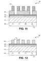
- FIG. 11shows the structure of FIG. 10 following the selective removal of the lamellar bodies to leave a patterned hard mask on the surface of the structure;
- FIG. 12shows the structure of FIG. 11 following the etching of the sacrificial substrate layer with the hard mask as a pattern
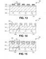
- FIG. 13shows the structure of FIG. 12 following the etching of the second hard mask layer using the patterned second substrate layer as a mask
- FIG. 14shows the structure of FIG. 13 following the forming of trenches in the ILD layer with the second hard mask 130 used as a mask;
- FIG. 15shows the structure of FIG. 14 following the introduction of interconnects in the trenches
- FIG. 16shows a cross-sectional side view of an integrated circuit structure according to another embodiment where a target material on the structure is used to pin two of particular block of a block copolymer.
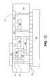
- FIG. 17is an interposer implementing one or more embodiments.
- FIG. 18illustrates an embodiment of a computing device.
- DSAdirected self-assembly
- a method of creating small pitch features using directed self-assembly (DSA) and creating tight-pitch interconnectsis disclosed.
- DSAis a process where a guide on a surface is used to align a lamellar block copolymer.
- a target materialis introduced that facilitates self-alignment of DSA materials to form a pattern.
- a target materialin one embodiment, is a material on a substrate such as a metal or other material that can be modified to attract a block (a polymer) of a DSA block copolymer relative to another material on the substrate and direct the self-alignment of the block copolymer.
- the target materialis patterned as loose pitch (large pitch) lines on a substrate and used as a template for a tighter pitch DSA patterning scheme.
- a methodincludes forming a target pattern of a target material on a surface of a substrate; depositing a block copolymer on the surface of the substrate, wherein one of two block (polymers) of the block copolymer preferentially aligns to the target material or a directed self-assembly promotion (DSAAP) layer on the target material and the two blocks of the copolymer self assemble after deposition into repeating lamellar bodies (alternating one after the other in a repeating pattern); selectively retaining one of the two blocks of the block copolymer over the other as a polymer pattern; and patterning the substrate with the polymer pattern.
- DSAAPdirected self-assembly promotion
- Patterning the substratecan include patterning one or more underlying sacrificial substrate layers to transfer the pattern to such one or more sacrificial substrate layers and etching openings in the substrate.
- the openings in the substratemay be filled with interconnect material.
- FIGS. 1-15describe one embodiment of forming an interconnect level or layer of a plurality of interconnects in an integrated circuit structure. More specifically, FIGS. 1-15 describe a process of pitch quartering using DSA with a single lithography pass and mask transfer layers.
- FIG. 1shows an embodiment of a portion of an integrated circuit structure. Such structure may be a portion of a wafer that is designated for hundreds of discrete integrated circuit chips.
- FIG. 1shows structure 100 including substrate 105 of, for example, a semiconductor material such as silicon, germanium, or other material.
- Substrate 105includes circuit devices, such as transistors and other devices (e.g., memory devices, capacitors) formed on a semiconductor surface and optionally one or more levels of interconnect to such circuit devices.
- Devices 110 in FIG. 1may be a circuit device (e.g., a transistor or other device) formed as part of a device level in or on a semiconductor substrate or on interconnect layer or level formed above a device level and connected to a lower level interconnect level and/or to a circuit device(s) at the device level through, for example, a conductive via. It is appreciated that techniques described herein may be used for various interconnects within an integrated circuit including interconnects to devices that include circuit devices and other interconnects. In this sense, devices 110 represents where an interconnect contact may be made.
- ILD layer 115Disposed on overlying a surface (top surface as viewed) of devices 110 and substrate 105 is interlayer dielectric (ILD) layer 115 as a feature layer.
- ILD layer 115is a silicon dioxide (SiO 2 ) or a dielectric material having a dielectric constant less than a dielectric constant of silicon dioxide (e.g., a “low k” material).
- Representative low k materialincludes materials containing silicon carbon and oxygen (e.g., polymers) that are known in the art.
- first hard mask layer 120Overlying ILD layer 115 , in this embodiment, is first hard mask layer 120 .
- First hard mask layer 120is, for example, a silicon nitride (Si x N y ) or other material that can serve, in one aspect, to protect underlying ILD layer 115 from undesired etching with respect to etch processes that may be performed on overlying layers.
- first hard mask layer 120has a thickness on the order of 5 nanometers (nm)-50 nm.
- second hard mask layer 130is a material that has an etch rate for a particular etchant that is different than a material for first hard mask layer 120 .
- first hard mask layer 120is silicon nitride
- a suitable material for second hard mask layer 130is titanium nitride (TiN).
- TiNtitanium nitride
- a representative thickness of second hard mask layer 130 of titanium nitrideis on the order of 5-50 nm.
- sacrificial substrate layer 140Overlying second hard mask layer 130 in the embodiment of structure 100 shown in FIG. 1 is sacrificial substrate layer 140 .
- sacrificial substrate layer 140may be used to accept an initial pitch pattern that will subsequently be reduced.
- sacrificial substrate layer 140is an oxide material (e.g., SiO 2 ) deposited to a thickness on the order of 5-50 nm.
- third hard mask layer 150is silicon nitride or other material that may serve, in one aspect, to protect sacrificial substrate layer 140 from undesired etching.
- fourth hard mask layer 160Overlying third hard mask layer 150 is fourth hard mask layer 160 .
- fourth hard mask layer 160is a material that has an etch rate different than an etch rate of third hard mask layer 150 for a particular etchant.
- third hard mask layer 150is a silicon nitride material
- fourth hard mask layer 160is a carbon hard mask (CHM) deposited to a representative thickness on the order of 100 nm.
- CHMcarbon hard mask
- Overlying fourth hard mask layer 160is anti-reflective coating layer 170 deposited to a thickness on the order of 30 nm.
- FIG. 1shows the structure after the patterning of photoresist layer 180 on a surface of structure 100 (on a surface of anti-reflective coating layer 170 ).
- photoresist layer 180e.g., a negative photoresist material
- openingsare formed of a width, W, on the order of 60 nanometers (nm) and a length (into the page) selected, in one embodiment, for a desired interconnect length.
- Openings 175are patterned with a pitch, P 1 , in one embodiment, on the order of 160 nm (from right edge to right edge as viewed).
- FIG. 2shows the structure of FIG. 1 following the patterning of third hard mask layer 150 through the mask defined by photoresist layer 180 .
- FIG. 2shows the structure of FIG. 1 following the removal of photoresist layer 180 , anti-reflective coating layer 170 and fourth hard mask layer 160 .
- the etchproceeds through third hard mask layer 150 to define openings 155 having a width, W, similar to the width of the openings through photoresist layer 180 (a 60 nm width) and a pitch, P 1 (e.g., on the order of 160 nm).
- FIG. 3shows the structure of FIG. 2 following the conformal deposition of spacer layer 185 on a surface of the structure.
- spacer layer 185is, for example, a material similar to sacrificial substrate layer 140 (e.g., an oxide).
- spacer layer 185is deposited by way of, for example, a chemical vapor deposition (CVD) process. The deposition is conformal in the sense that the deposited layer conforms to the surface of the substrate including on third hard mask layer 150 and onto a surface of sacrificial substrate layer 140 .
- a representative thickness, t, of spacer layer 185is on the order of 20 nm.
- FIG. 4shows the structure of FIG. 3 following the etching of spacer layer 185 .
- spacer layer 185is etched by an anisotropic etchant, which, as viewed, etches vertically.
- a suitable anisotropic etchant where spacer layer 185 and sacrificial substrate layer are each an oxideis carbon tetrafluoride (CF 4 ).
- FIG. 4shows that following an anisotropic etch, spacer layer 185 is removed from a surface of third hard mask layer 150 and a base of opening 155 .
- Width W 2is less than width, W originally established by the pattern of photoresist layer 180 . Where width W was 60 nm, and spacer layer 185 has a thickness of 20 nm, width, W 2 is 20 nm (60 nm-20 nm-20 nm).
- FIG. 5shows the structure of FIG. 4 following the deposition of a target material over the surface and in opening 190 .
- target material 195is a metal or other material that can be selectively modified relative to a material of sacrificial substrate layer 140 to favor the alignment of one polymer of a DSA block copolymer to the target material over the other.
- Representative metalsinclude but are not limited to, tungsten, copper, titanium, titanium nitride, cobalt, ruthenium and aluminum. In one embodiment, tungsten is selected.
- Representative other materialsinclude dielectric materials (e.g., Si 3 N 4 , SiO 2 , SiCN, low k dielectric materials). Where sacrificial substrate layer 140 is a dielectric material, target material 195 of a dielectric will be a different dielectric material that can be selectively modified relative to sacrificial substrate layer 140 .
- FIG. 6shows the structure of FIG. 5 following the planarization of the substrate surface.
- FIG. 6shows the removal of target material from a surface of the structure leaving such target material 195 in openings 190 and also the removal of third hard mask layer 195 and spacer layer 185 .
- One technique for planarizing substrateis a chemical mechanical polish.
- FIG. 6shows superior surface 145 of the structure defined by sacrificial substrate layer 140 and periodically spaced lines of target material 195 .
- an exposed surface of target material 195may optimally be cleaned.
- the surfacemay be cleaned by etch or wash to remove any oxidized material.
- FIG. 7shows the structure of FIG. 6 following the introduction of a directed self-assembly promotion (DSAAP) layer such as a pretreatment brush on a surface of target material 195 and not on a surface of sacrificial substrate layer 140 .
- DSAAP layer 200is tailored for one of a block (polymer) of a block copolymer of a DSA material to be subsequently introduced on the structure so that the one block will have an affinity for attachment (alignment) to DSAAP layer 200 .
- Such a DSAAP layer materialis introduced to, in one embodiment, control an interaction of a subsequently introduced polymer of a block copolymer on the substrate.
- DSAAP layer 200serves to orient and register the lamellar bodies of the block composition.
- DSAAP layer 200is a polymer based on a similar monomer of one block of a block copolymer to be subsequently introduced.
- a block copolymeris polystyrene (PS)/polymethyl methacrylate (PMMA)
- DSAAP layer 200is a polymer based on either PS or PMMA.
- DSAAP layer 200includes a reactive group such as hydroxyl groups that react with target material 195 .
- DSAAP layer 200may be introduced to a thickness on the order of 5 nm to 10 nm.
- One techniqueis to apply the polymer as a liquid, bake and remove (rinse) any excess (any unreacted polymer).
- FIG. 7also shows the structure after the optional introduction of DSAAP layer 210 such as a neutral brush.
- DSAAP layer 210such as a neutral brush.
- alignment control of a DSA process to achieve a vertical orientation of each block of a block copolymeris desired.
- One way to achieve vertical orientationis to control the interaction between the block copolymer-substrate interface and the block copolymer-air interface.
- the block copolymer-air interfaceis a function of the surface energies of the blocks of the copolymer.
- the polymershave similar surface energies which creates a generally neutral polymer-air interface.
- a substrate surfacesuch as a surface of sacrificial substrate layer 140 may have a higher surface energy than the polymers of the block copolymer.
- DSAAP layer 210 of a neutral brushmay be introduced to reduce the surface energy of the substrate and generally equate such surface energy with that of the blocks of the block copolymer.
- DSAAP layer 210includes reactive groups such as hydroxyl groups to react with a surface of sacrificial substrate layer 140 .
- DSAAP layer 210may be deposited to a thickness on the order of 5 nm-10 nm as a liquid, baked and any excess removed by rinsing.
- FIG. 8shows the structure of FIG. 7 following the introduction of a block copolymer and the DSA process.
- FIG. 8shows block copolymer 220 of, for example, a PS/PMMA introduced by spin-on process on a surface of the structure (a top surface as viewed).
- FIG. 8shows that DSA block copolymer 220 aligns based on DSAAP layer 200 .
- DSAAP layer 200favored the PS block of the block copolymer relative to the PMMA block
- the PS blockwill align with DSAAP layer 200 (attach to DSAAP layer 200 ).
- the alignmentserves to orient the blocks as repeating lamellar bodies alternating one after the other in a repeating pattern across the surface of the substrate.
- FIG. 8shows block copolymer 220 of, for example, a PS/PMMA introduced by spin-on process on a surface of the structure (a top surface as viewed).
- FIG. 8shows that DSA block copolymer 220 aligns based on DSAAP
- lamellar body 2202 of, for example, PS and lamellar body 2204 of PMMAEach lamellar body is vertically oriented relative to a surface of sacrificial substrate layer 140 of the structure.
- a molecular weight of the blocks (polymers) of a composition of DSA block copolymer 220is tuned so that each lamellar body has a width, W 2 , equal to a width of the target material.
- FIG. 9shows the structure of FIG. 8 following the removal of the PMMA lamellar bodies (PMMA blocks) and the hardening of PS lamellar bodies (PS blocks 2202 ).
- the lamellar bodiesare hardened by a curing (e.g., a thermal cure).
- PMMA lamellar bodiesmay be removed by dry etch.
- FIG. 9shows that following the removal of the PMMA lamellar bodies, a pitch between similar edges of PS lamellar bodies (e.g., a right edge as shown) is P 2 .
- the pitch, P 2is one-fourth the pitch, P 1 .
- FIG. 10shows the structure of FIG. 9 following the introduction of a hard mask material complementary to the polymer pattern.
- FIG. 10shows hard mask 230 of, for example, silicon nitride deposited in a complementary fashion in the sense that hard mask layer 230 complements or completes in a sense a layer on a surface of the structure with PS lamellar bodies 2202 .
- FIG. 11shows the structure of FIG. 10 following the selective removal of PS lamellar bodies 2202 to leave patterned hard mask 230 on the surface of the structure.
- PS lamellar bodies 2202may be removed by an ashing process.
- FIG. 11also shows the structure following the removal of target material 195 .
- target materialsuch as tungsten
- such materialmay be removed by a chemical etch.
- FIG. 12shows the structure of FIG. 11 following the etching of sacrificial substrate layer 140 with hard mask 230 as a pattern.
- the etchis an anisotropic etch (e.g., CF 4 for a sacrificial substrate layer of SiO 2 ) and selectively stops on second hard mask layer 130 .
- FIG. 12shows the structure following the removal of hard mask layers 230 and illustrates that sacrificial substrate layer 230 is patterned into structures having a pitch P 2 (measured right edge to right edge as viewed).
- FIG. 13shows the structure of FIG. 12 following the etching of second hard mask layer 130 using the patterned second substrate layer 140 as a mask. In this manner, the pattern of sacrificial substrate layer 140 is transferred to second hard mask layer 130 .
- a suitable etchant to remove a second hard mask layer of TiN selective to a material for first hard mask layer 120 of silicon nitrideis chlorine/argon Cl 2 /Ar.
- FIG. 14shows the structure of FIG. 13 following a trench etch of ILD layer 115 .
- patterned second hard mask 130is used as a mask and an etch proceeds through first hard mask layer 120 and into a desired depth of ILD layer 115 to form trenches 250 in the ILD layer.
- vias 260may subsequently be formed through ILD layer 115 to devices 110 by, for example, patterns of a mask (e.g., a photoresist) over areas of a surface of the substrate, the etching to devices 110 and then remove the mask.
- FIG. 14shows the structure after trench (and via) formation after the removal of second hard mask layer 130 .
- FIG. 15shows the structure of FIG. 14 following the introduction of interconnects 250 in trenches 250 .
- interconnects 250are an electrically conductive copper material introduced by an electroplating process.
- trenches 245are seeded with a conductive seed material followed by plating of the interconnect material.
- Conductive vias 260may be formed at a similar time.
- vias 260may be formed prior to the formation of trenches 250 .
- conductive vias 260may be a tungsten material introduced by a deposition process.
- the above method of pitch quarteringuses DSA with a target material patterned as lines of loose pitch (larger pitch) as a guide or template in one technique for creating tight-pitched interconnect features.
- the method of using a target material as a guide for a chemically-selective DSAAP layer (e.g., a pretreatment brush) than spinning on a DSA material that selectively aligns to the target material over other material forming a surface of a structurecan be used to produce pitches of other divisions of an original pitch, such as 1 ⁇ 2, 1 ⁇ 3, 1 ⁇ 5, 1 ⁇ 6, etc., an original loose pitch.
- the target materialcan be either sacrificial (as in the above method) or a permanent feature.
- the DSA polymerscan be ones of various combinations of block copolymers. If spun-on during different alignment operations, multiple pitches can be patterned with multiple DSA materials.
- a target material(target material 190 ) was used to target or pin a single body of one block of a DSA block copolymer.
- a target materialcan be used to target or pin more than one body of one block of a DSA block copolymer.
- FIG. 16shows an embodiment of the structure analogous to FIG. 8 above where like reference numerals refer to like materials.
- a width, W T of target material 195is greater than a width of a block of a DSA copolymer that is targeted so that multiple ones of the particular block are formed on the target material.
- DSAAP layer 2000disposed on a surface of target material 195 of, for example, a metal is DSAAP layer 2000 that, in one embodiment, favors or prefers the alignment of one block of the block copolymer over the other.
- DSAAP layer 2000is similar to DSAAP layer 200 described above in that one block of a DSA block copolymer prefers it over the other.
- DSAAP layer 2000is a material that one block of a DSA block copolymer slightly prefers over the other.
- FIG. 16also shows DSAAP layer 2100 disposed on a surface of dielectric layer 140 .
- DSAAP layer 2100may be similar to DSAAP layer 210 (see FIG.
- DSAAP layer 2100may be selected of a material that one block of a DSA block copolymer slightly prefers the material over the other (the block that did not prefer DSAAP layer 2000 prefers DSAAP layer 2100 ).
- FIG. 16shows the structure after introduction of DSA block copolymer such as PS/PMMA and shows the assembly of the polymer into lamellar bodies across a surface of the substrate.
- one block of a DSA block copolymere.g., PS
- two bodies 2202 of the one blocke.g., PS
- Two bodies 2202 of the one blocke.g., PS
- body 2204 of the other block of the DSA block copolymere.g., PMMA
- the lamellar bodiesform a pattern of alternating bodies, one body after the other, across the surface of the structure similar to that described above with respect to FIG. 8 .
- the width of a blockis dependent on a molecular weight of a polymer in the block copolymer.
- FIG. 17illustrates interposer 300 that includes one or more embodiments.
- Interposer 300is an intervening substrate used to bridge a first substrate 302 to second substrate 304 .
- First substrate 302may be, for instance, an integrated circuit die including interconnects formed using the DSA technique described above.
- Second substrate 304may be, for instance, a memory module, a computer motherboard, or another integrated circuit die.
- the purpose of interposer 300is to spread a connection to a wider pitch or to reroute a connection to a different connection.
- interposer 300may couple an integrated circuit die to ball grid array (BGA) 306 that can subsequently be coupled to second substrate 304 .
- BGAball grid array
- first and second substrates 302 / 304are attached to opposing sides of interposer 300 . In other embodiments, first and second substrates 302 / 304 are attached to the same side of interposer 300 . In further embodiments, three or more substrates are interconnected by way of interposer 300 .
- Interposer 300may be formed of an epoxy resin, a fiberglass-reinforced epoxy resin, a ceramic material, or a polymer material such as polyimide.
- the interposermay be formed of alternate rigid or flexible materials that may include the same materials described above for use in a semiconductor substrate, such as silicon, germanium, and other group III-V and group IV materials.
- the interposermay include metal interconnects 308 and vias 310 , including but not limited to through-silicon vias (TSVs) 312 .
- Interposer 300may further include embedded devices 314 , including both passive and active devices. Such devices include, but are not limited to, capacitors, decoupling capacitors, resistors, inductors, fuses, diodes, transformers, sensors, and electrostatic discharge (ESD) devices. More complex devices such as radio-frequency (RF) devices, power amplifiers, power management devices, antennas, arrays, sensors, and MEMS devices may also be formed on interposer 300 .
- RFradio-frequency
- FIG. 18illustrates computing device 400 in accordance with one embodiment.
- Computing device 400may include a number of components. In one embodiment, these components are attached to one or more motherboards. In an alternate embodiment, these components are fabricated onto a single system-on-a-chip (SoC) die rather than a motherboard.
- the components in computing device 400include, but are not limited to, integrated circuit die 402 and at least one communication chip 408 . In some implementations communication chip 408 is fabricated as part of integrated circuit die 402 .
- Integrated circuit die 402may include CPU 404 as well as on-die memory 406 , often used as cache memory, that can be provided by technologies such as embedded DRAM (eDRAM) or spin-transfer torque memory (STTM or STTM-RAM).
- eDRAMembedded DRAM
- STTM or STTM-RAMspin-transfer torque memory
- Computing device 400may include other components that may or may not be physically and electrically coupled to the motherboard or fabricated within an SoC die. These other components include, but are not limited to, volatile memory 410 (e.g., DRAM), non-volatile memory 412 (e.g., ROM or flash memory), graphics processing unit 414 (GPU), digital signal processor 416 , crypto processor 442 (a specialized processor that executes cryptographic algorithms within hardware), chipset 420 , antenna 422 , display or a touchscreen display 424 , touchscreen controller 426 , battery 428 or other power source, a power amplifier (not shown), global positioning system (GPS) device 444 , compass 430 , motion coprocessor or sensors 432 (that may include an accelerometer, a gyroscope, and a compass), speaker 434 , camera 436 , user input devices 438 (such as a keyboard, mouse, stylus, and touchpad), and mass storage device 440 (such as hard disk drive, compact disk (CD), digital versatile
- Communications chip 408enables wireless communications for the transfer of data to and from computing device 400 .
- the term “wireless” and its derivativesmay be used to describe circuits, devices, systems, methods, techniques, communications channels, etc., that may communicate data through the use of modulated electromagnetic radiation through a non-solid medium. The term does not imply that the associated devices do not contain any wires, although in some embodiments they might not.
- Communication chip 408may implement any of a number of wireless standards or protocols, including but not limited to Wi-Fi (IEEE 802.11 family), WiMAX (IEEE 802.16 family), IEEE 802.20, long term evolution (LTE), Ev-DO, HSPA+, HSDPA+, HSUPA+, EDGE, GSM, GPRS, CDMA, TDMA, DECT, Bluetooth, derivatives thereof, as well as any other wireless protocols that are designated as 3G, 4G, 5G, and beyond.
- Computing device 400may include a plurality of communication chips 408 .
- a first communication chipmay be dedicated to shorter range wireless communications such as Wi-Fi and Bluetooth and a second communication chip may be dedicated to longer range wireless communications such as GPS, EDGE, GPRS, CDMA, WiMAX, LTE, Ev-DO, and others.
- Processor 404 of computing device 400includes one or more devices, such as transistors or metal interconnects. Metal interconnects are formed in accordance with embodiments described above using DSA for pitch division.
- the term “processor”may refer to any device or portion of a device that processes electronic data from registers and/or memory to transform that electronic data into other electronic data that may be stored in registers and/or memory.
- Communication chip 408may also include one or more devices, such as transistors or metal interconnects. Metal interconnects are that are formed in accordance with embodiments.
- another component housed within computing device 400may contain one or more devices, such as transistors or metal interconnects.
- Metal interconnectsare formed in accordance with implementations.
- computing device 400may be a laptop computer, a netbook computer, a notebook computer, an ultrabook computer, a smartphone, a tablet, a personal digital assistant (PDA), an ultra mobile PC, a mobile phone, a desktop computer, a server, a printer, a scanner, a monitor, a set-top box, an entertainment control unit, a digital camera, a portable music player, or a digital video recorder.
- computing device 1200may be any other electronic device that processes data.
- Example 1is a method including forming a target pattern of a target material on a surface of a substrate; depositing a block copolymer on the surface of the substrate, wherein one of two blocks of the block copolymer preferentially aligns to the target material and the two blocks self assemble after deposition into repeating lamellar bodies on the surface of the substrate; selectively retaining one of the two blocks of the block copolymer over the other as a polymer pattern; and patterning the substrate with the polymer pattern.
- Example 2the target material of the method of Example 1 includes a metal.
- Example 3the metal of the method of Example 2 is selected from the group consisting of tungsten, copper, titanium, titanium nitride, cobalt, ruthenium and aluminum.
- Example 4prior to depositing the block copolymer on the surface of the substrate, the method of any of Examples 1-3 includes depositing a directed self-assembly alignment promotion (DSAAP) layer tailored for one of the blocks of the block copolymer on the target material.
- DSAAPdirected self-assembly alignment promotion
- the DSAAP layer of the method of Example 4is a first DSAAP layer and prior to depositing the block copolymer on the surface of the substrate, the method further includes depositing a second DSAAP layer that does not have a greater affinity for one of the blocks of the block copolymer on the surface of the substrate in an area free of the first DSAAP layer.
- patterning the substrate with the polymer pattern of the method of any of Examples 1-4includes depositing a sacrificial material complementary to the polymer pattern; removing the polymer pattern while leaving the sacrificial material as a complementary pattern on the substrate; and etching the substrate with the complementary pattern as a mask.
- the substrate of the method of Example 6includes a feature layer and at least one sacrificial substrate layer and etching the substrate with the complementary pattern as a mask includes etching the at least one sacrificial substrate layer.
- Example 8the target pattern of the method of any of Examples 1-7 includes a pitch that is greater than a pitch of the polymer pattern.
- Example 9selectively retaining one of the two blocks of the block copolymer of the method of any of Examples 1-8 includes selectively retaining the one with the affinity for the target material.
- Example 10is a method including forming a target pattern of a target material on a surface of a substrate, the target pattern including a first pitch; depositing a directed self-assembly alignment promotion (DSAAP) layer tailored for one of two blocks of a block copolymer on the target material; depositing a block copolymer on the surface of the substrate, wherein one of two blocks of the block copolymer aligns to the target material and the two blocks self assemble after deposition into repeating lamellar bodies on the surface of the substrate with an orientation perpendicular to the substrate; selectively removing the one of the two blocks of the block copolymer without the affinity for the target material to leave the other as a polymer pattern with a second pitch that is less than the first pitch; and patterning the substrate with the polymer pattern.
- DSAAPdirected self-assembly alignment promotion
- the target material of the method of Example 10includes a metal.
- Example 12the metal of the method of Example 11 is selected from the group consisting of tungsten, copper, titanium, titanium nitride, cobalt, rutherium and aluminum.
- the DSAAP layer of the method of Example 10is a first DSAAP layer and prior to depositing the block copolymer on the surface of the substrate, the method includes depositing a second DSAAP layer on the surface of the substrate in areas other than on the target material, wherein the DSAAP layer does not have a greater affinity for one of the blocks of the block copolymer on the target material.
- patterning the substrate with the polymer pattern of the method of Example 10includes depositing a sacrificial material complementary to the polymer pattern; removing the polymer pattern while leaving the sacrificial material as a complementary pattern on the substrate; and etching the substrate with the complementary pattern as a mask.
- the substrate of the method of Example 14includes a feature layer and at least one sacrificial substrate layer and etching the substrate with the complementary pattern as a mask includes etching the at least one sacrificial substrate layer.
- Example 16is a method including forming a target pattern of a target material on a surface of a substrate, the target pattern including a first pitch; depositing a block copolymer on the surface of the substrate, wherein one of two blocks of the block copolymer aligns to the target material and the two blocks self assemble after deposition into repeating lamellar bodies with an orientation perpendicular to the substrate; selectively removing the one of the two blocks of the block copolymer to leave the other as a polymer pattern; depositing a sacrificial material complementary to the polymer pattern; removing the polymer pattern while leaving the sacrificial material as a complementary pattern on the substrate; etching openings in the substrate with the complementary pattern as a mask, the polymer pattern including a second pitch that is less than the first pitch; and forming interconnects in the openings.
- the substrate of the method of Example 16includes a dielectric layer and etching openings in the substrate includes etching openings in the dielectric layer.
- Example 18the target material of the method of Example 16 includes a metal.
- Example 19the metal of the method of Example 18 is selected from the group consisting of tungsten, copper, titanium, titanium nitride, cobalt, ruthenium and aluminum.
- Example 20prior to depositing the block copolymer on the surface of the substrate, the method of Example 16 includes depositing a directed self-assembly alignment promotion (DSAAP) layer tailored for one of the blocks of the block copolymer on the target material.
- DSAAPdirected self-assembly alignment promotion
- the DSAAP layer of the method of Example 20is a first DSAAP layer and prior to depositing the block copolymer on the surface of the substrate, the method further includes depositing a second DSAAP layer that does not have a greater affinity for one of the blocks of the block copolymer on the surface of the substrate in areas other than on the surface of target material.
- Example 22is an apparatus including an integrated circuit substrate including a plurality of contact points and a dielectric layer on the contact points; a target pattern formed in a surface of the dielectric layer; and a self-assembled layer of repeating alternating bodies of a block copolymer, wherein one of two blocks of the block copolymer is preferentially aligned to the target pattern.
- Example 23the apparatus of Example 22 further includes a directed self assembly alignment promotion (DSAAP) layer tailored for one of the blocks of the block copolymer on the target pattern between the target pattern and the self assembled layer.
- DSAAPdirected self assembly alignment promotion
- the DSAAP layer of the apparatus of Example 23is a first DSAAP layer and the apparatus further includes a second DSAAP layer that does not have a greater affinity for one of the blocks of the block copolymer on the surface of the substrate free of the target pattern.
- Example 25the target pattern of the apparatus of Example 22 includes a metal.
- Example 26the metal of the apparatus of Example 25 is selected from the group consisting of tungsten, copper, titanium, titanium nitride, cobalt, ruthenium and aluminum.
- Example 27the target pattern of the apparatus of any of Examples 22-26 includes a plurality of lines disposed at a first pitch that is greater than a pitch of one of the alternating bodies of the block copolymer.
Landscapes
- Engineering & Computer Science (AREA)
- Physics & Mathematics (AREA)
- General Physics & Mathematics (AREA)
- Condensed Matter Physics & Semiconductors (AREA)
- Manufacturing & Machinery (AREA)
- Computer Hardware Design (AREA)
- Microelectronics & Electronic Packaging (AREA)
- Power Engineering (AREA)
- Chemical & Material Sciences (AREA)
- Inorganic Chemistry (AREA)
- Internal Circuitry In Semiconductor Integrated Circuit Devices (AREA)
Abstract
Description
- Integrated circuit processes.
- Lithography is not generally scaling in pace with Moore's law. The current process technologies typically use a spacer based method of pitch division to create small pitch features. With the current state of art, resulting features exhibit generally poor critical dimension uniformity (CDU), are increasingly expensive to manufacture, and exhibit generally poor line edge roughness (LER).
FIG. 1 shows a cross-sectional side view of a portion of an integrated circuit structure, including a substrate, circuit devices and one or more optional interconnect levels, an interlayer dielectric layer, and first, second and third layers of mask layers, a sacrificial substrate layer, an antirefelction layer and a photoresist layer patterned with a first pitch thereon;FIG. 2 shows the structure ofFIG. 1 following the patterning of a third hard mask layer through the mask defined by photoresist layer;FIG. 3 shows the structure ofFIG. 2 following the conformal deposition of a spacer layer on a surface of the structure;FIG. 4 shows the structureFIG. 3 following the anisotropic etching of the spacer layer, a removal of the third hard mask layer and the forming openings through the sacrificial substrate layer;FIG. 5 shows the structure ofFIG. 4 following the deposition of a target material over the surface and in the openings through the sacrificial substrate layer;FIG. 6 shows the structure ofFIG. 5 following the planarization of the substrate surface to remove the target material from a surface of the structure;FIG. 7 shows the structure ofFIG. 6 following the introduction of a directed self-assembly alignment promotion (DSAAP) layer on a surface oftarget material 195 where such DSAAP is tailored for one of a block (a polymer) of a block copolymer of a DSA material to be subsequently introduced and the introduction of a neutral DSAAP;FIG. 8 shows the structure ofFIG. 7 following the introduction of a block copolymer on the structure according to a DSA process that forms repeating alternating lamellar bodies of the blocks of the block copolymer;FIG. 9 shows the structure ofFIG. 8 following the selective removal of one of the lamellar bodies and the hardening of the retained lamellar bodies to form a polymer pattern;FIG. 10 shows the structure ofFIG. 9 following the introduction of a hard mask complementary to the polymer pattern;FIG. 11 shows the structure ofFIG. 10 following the selective removal of the lamellar bodies to leave a patterned hard mask on the surface of the structure;FIG. 12 shows the structure ofFIG. 11 following the etching of the sacrificial substrate layer with the hard mask as a pattern;FIG. 13 shows the structure ofFIG. 12 following the etching of the second hard mask layer using the patterned second substrate layer as a mask;FIG. 14 shows the structure ofFIG. 13 following the forming of trenches in the ILD layer with the secondhard mask 130 used as a mask;FIG. 15 shows the structure ofFIG. 14 following the introduction of interconnects in the trenches;FIG. 16 shows a cross-sectional side view of an integrated circuit structure according to another embodiment where a target material on the structure is used to pin two of particular block of a block copolymer.FIG. 17 is an interposer implementing one or more embodiments; andFIG. 18 illustrates an embodiment of a computing device.- A method of creating small pitch features using directed self-assembly (DSA) and creating tight-pitch interconnects is disclosed. DSA is a process where a guide on a surface is used to align a lamellar block copolymer. In one embodiment, a target material is introduced that facilitates self-alignment of DSA materials to form a pattern. A target material, in one embodiment, is a material on a substrate such as a metal or other material that can be modified to attract a block (a polymer) of a DSA block copolymer relative to another material on the substrate and direct the self-alignment of the block copolymer. In one embodiment, the target material is patterned as loose pitch (large pitch) lines on a substrate and used as a template for a tighter pitch DSA patterning scheme. A method includes forming a target pattern of a target material on a surface of a substrate; depositing a block copolymer on the surface of the substrate, wherein one of two block (polymers) of the block copolymer preferentially aligns to the target material or a directed self-assembly promotion (DSAAP) layer on the target material and the two blocks of the copolymer self assemble after deposition into repeating lamellar bodies (alternating one after the other in a repeating pattern); selectively retaining one of the two blocks of the block copolymer over the other as a polymer pattern; and patterning the substrate with the polymer pattern. Patterning the substrate can include patterning one or more underlying sacrificial substrate layers to transfer the pattern to such one or more sacrificial substrate layers and etching openings in the substrate. In one embodiment, the openings in the substrate may be filled with interconnect material.
FIGS. 1-15 describe one embodiment of forming an interconnect level or layer of a plurality of interconnects in an integrated circuit structure. More specifically,FIGS. 1-15 describe a process of pitch quartering using DSA with a single lithography pass and mask transfer layers. Referring toFIG. 1 ,FIG. 1 shows an embodiment of a portion of an integrated circuit structure. Such structure may be a portion of a wafer that is designated for hundreds of discrete integrated circuit chips.FIG. 1 showsstructure 100 includingsubstrate 105 of, for example, a semiconductor material such as silicon, germanium, or other material.Substrate 105, in one embodiment, includes circuit devices, such as transistors and other devices (e.g., memory devices, capacitors) formed on a semiconductor surface and optionally one or more levels of interconnect to such circuit devices.Devices 110 inFIG. 1 may be a circuit device (e.g., a transistor or other device) formed as part of a device level in or on a semiconductor substrate or on interconnect layer or level formed above a device level and connected to a lower level interconnect level and/or to a circuit device(s) at the device level through, for example, a conductive via. It is appreciated that techniques described herein may be used for various interconnects within an integrated circuit including interconnects to devices that include circuit devices and other interconnects. In this sense,devices 110 represents where an interconnect contact may be made.- Disposed on overlying a surface (top surface as viewed) of
devices 110 andsubstrate 105 is interlayer dielectric (ILD)layer 115 as a feature layer. In one embodiment,ILD layer 115 is a silicon dioxide (SiO2) or a dielectric material having a dielectric constant less than a dielectric constant of silicon dioxide (e.g., a “low k” material). Representative low k material includes materials containing silicon carbon and oxygen (e.g., polymers) that are known in the art. OverlyingILD layer 115, in this embodiment, is firsthard mask layer 120. Firsthard mask layer 120 is, for example, a silicon nitride (SixNy) or other material that can serve, in one aspect, to protectunderlying ILD layer 115 from undesired etching with respect to etch processes that may be performed on overlying layers. In one embodiment, firsthard mask layer 120 has a thickness on the order of 5 nanometers (nm)-50 nm. - Overlying first
hard mask layer 120 in the embodiment ofstructure 100 inFIG. 1 is secondhard mask layer 130. In one embodiment, secondhard mask layer 130 is a material that has an etch rate for a particular etchant that is different than a material for firsthard mask layer 120. Where firsthard mask layer 120 is silicon nitride, a suitable material for secondhard mask layer 130 is titanium nitride (TiN). A representative thickness of secondhard mask layer 130 of titanium nitride is on the order of 5-50 nm. - Overlying second
hard mask layer 130 in the embodiment ofstructure 100 shown inFIG. 1 issacrificial substrate layer 140. In one embodiment,sacrificial substrate layer 140 may be used to accept an initial pitch pattern that will subsequently be reduced. In one embodiment,sacrificial substrate layer 140 is an oxide material (e.g., SiO2) deposited to a thickness on the order of 5-50 nm. Overlyingsacrificial substrate layer 140 is thirdhard mask layer 150. In one embodiment, thirdhard mask layer 150 is silicon nitride or other material that may serve, in one aspect, to protectsacrificial substrate layer 140 from undesired etching. Overlying thirdhard mask layer 150 is fourthhard mask layer 160. In one embodiment, fourthhard mask layer 160 is a material that has an etch rate different than an etch rate of thirdhard mask layer 150 for a particular etchant. In one embodiment, where thirdhard mask layer 150 is a silicon nitride material, fourthhard mask layer 160 is a carbon hard mask (CHM) deposited to a representative thickness on the order of 100 nm. Overlying fourthhard mask layer 160 isanti-reflective coating layer 170 deposited to a thickness on the order of 30 nm. FIG. 1 shows the structure after the patterning ofphotoresist layer 180 on a surface of structure100 (on a surface of anti-reflective coating layer170). As illustrated, photoresist layer180 (e.g., a negative photoresist material) is patterned to include openings through the photoresist toanti-reflective coating layer 170. In one embodiment, openings are formed of a width, W, on the order of 60 nanometers (nm) and a length (into the page) selected, in one embodiment, for a desired interconnect length.Openings 175 are patterned with a pitch, P1, in one embodiment, on the order of 160 nm (from right edge to right edge as viewed).FIG. 2 shows the structure ofFIG. 1 following the patterning of thirdhard mask layer 150 through the mask defined byphotoresist layer 180.FIG. 2 shows the structure ofFIG. 1 following the removal ofphotoresist layer 180,anti-reflective coating layer 170 and fourthhard mask layer 160. The etch proceeds through thirdhard mask layer 150 to defineopenings 155 having a width, W, similar to the width of the openings through photoresist layer180 (a 60 nm width) and a pitch, P1(e.g., on the order of 160 nm).FIG. 3 shows the structure ofFIG. 2 following the conformal deposition ofspacer layer 185 on a surface of the structure. In one embodiment,spacer layer 185 is, for example, a material similar to sacrificial substrate layer140 (e.g., an oxide). In one embodiment,spacer layer 185 is deposited by way of, for example, a chemical vapor deposition (CVD) process. The deposition is conformal in the sense that the deposited layer conforms to the surface of the substrate including on thirdhard mask layer 150 and onto a surface ofsacrificial substrate layer 140. A representative thickness, t, ofspacer layer 185 is on the order of 20 nm.FIG. 4 shows the structure ofFIG. 3 following the etching ofspacer layer 185. In one embodiment,spacer layer 185 is etched by an anisotropic etchant, which, as viewed, etches vertically. A suitable anisotropic etchant wherespacer layer 185 and sacrificial substrate layer are each an oxide is carbon tetrafluoride (CF4).FIG. 4 shows that following an anisotropic etch,spacer layer 185 is removed from a surface of thirdhard mask layer 150 and a base ofopening 155.FIG. 4 also shows a structure following a further anisotropic etch ofstructure 100 to reduce a thickness of thirdhard mask layer 150 and remaining vertical portions ofspacer layer 185 while formingopening 190 throughsacrificial substrate layer 140. The opening throughsacrificial substrate layer 140 has a width W2. Width W2, is less than width, W originally established by the pattern ofphotoresist layer 180. Where width W was 60 nm, andspacer layer 185 has a thickness of 20 nm, width, W2is 20 nm (60 nm-20 nm-20 nm).FIG. 5 shows the structure ofFIG. 4 following the deposition of a target material over the surface and inopening 190. In one embodiment,target material 195 is a metal or other material that can be selectively modified relative to a material ofsacrificial substrate layer 140 to favor the alignment of one polymer of a DSA block copolymer to the target material over the other. Representative metals include but are not limited to, tungsten, copper, titanium, titanium nitride, cobalt, ruthenium and aluminum. In one embodiment, tungsten is selected. Representative other materials include dielectric materials (e.g., Si3N4, SiO2, SiCN, low k dielectric materials). Wheresacrificial substrate layer 140 is a dielectric material,target material 195 of a dielectric will be a different dielectric material that can be selectively modified relative tosacrificial substrate layer 140.FIG. 6 shows the structure ofFIG. 5 following the planarization of the substrate surface.FIG. 6 shows the removal of target material from a surface of the structure leavingsuch target material 195 inopenings 190 and also the removal of thirdhard mask layer 195 andspacer layer 185. One technique for planarizing substrate is a chemical mechanical polish.FIG. 6 showssuperior surface 145 of the structure defined bysacrificial substrate layer 140 and periodically spaced lines oftarget material 195. At this point, an exposed surface oftarget material 195 may optimally be cleaned. For example, wheretarget material 195 is a metal subject to oxidation, the surface may be cleaned by etch or wash to remove any oxidized material.FIG. 7 shows the structure ofFIG. 6 following the introduction of a directed self-assembly promotion (DSAAP) layer such as a pretreatment brush on a surface oftarget material 195 and not on a surface ofsacrificial substrate layer 140. In one embodiment,DSAAP layer 200 is tailored for one of a block (polymer) of a block copolymer of a DSA material to be subsequently introduced on the structure so that the one block will have an affinity for attachment (alignment) toDSAAP layer 200. Such a DSAAP layer material is introduced to, in one embodiment, control an interaction of a subsequently introduced polymer of a block copolymer on the substrate.DSAAP layer 200 serves to orient and register the lamellar bodies of the block composition. Representatively,DSAAP layer 200 is a polymer based on a similar monomer of one block of a block copolymer to be subsequently introduced. Representatively, where a block copolymer is polystyrene (PS)/polymethyl methacrylate (PMMA),DSAAP layer 200 is a polymer based on either PS or PMMA. In one embodiment,DSAAP layer 200 includes a reactive group such as hydroxyl groups that react withtarget material 195. Representatively,DSAAP layer 200 may be introduced to a thickness on the order of 5 nm to 10 nm. One technique is to apply the polymer as a liquid, bake and remove (rinse) any excess (any unreacted polymer).FIG. 7 also shows the structure after the optional introduction ofDSAAP layer 210 such as a neutral brush. Generally speaking, alignment control of a DSA process to achieve a vertical orientation of each block of a block copolymer is desired. One way to achieve vertical orientation is to control the interaction between the block copolymer-substrate interface and the block copolymer-air interface. The block copolymer-air interface is a function of the surface energies of the blocks of the copolymer. For a block copolymer of PS and PMMA, the polymers have similar surface energies which creates a generally neutral polymer-air interface. A substrate surface such as a surface ofsacrificial substrate layer 140 may have a higher surface energy than the polymers of the block copolymer. In one embodiment,DSAAP layer 210 of a neutral brush may be introduced to reduce the surface energy of the substrate and generally equate such surface energy with that of the blocks of the block copolymer. In one embodiment,DSAAP layer 210 includes reactive groups such as hydroxyl groups to react with a surface ofsacrificial substrate layer 140.DSAAP layer 210 may be deposited to a thickness on the order of 5 nm-10 nm as a liquid, baked and any excess removed by rinsing.FIG. 8 shows the structure ofFIG. 7 following the introduction of a block copolymer and the DSA process.FIG. 8 showsblock copolymer 220 of, for example, a PS/PMMA introduced by spin-on process on a surface of the structure (a top surface as viewed).FIG. 8 shows thatDSA block copolymer 220 aligns based onDSAAP layer 200. Representatively, whereDSAAP layer 200 favored the PS block of the block copolymer relative to the PMMA block, the PS block will align with DSAAP layer200 (attach to DSAAP layer200). The alignment serves to orient the blocks as repeating lamellar bodies alternating one after the other in a repeating pattern across the surface of the substrate.FIG. 8 showslamellar body 2202 of, for example, PS andlamellar body 2204 of PMMA. Each lamellar body is vertically oriented relative to a surface ofsacrificial substrate layer 140 of the structure. In one embodiment, a molecular weight of the blocks (polymers) of a composition ofDSA block copolymer 220 is tuned so that each lamellar body has a width, W2, equal to a width of the target material.FIG. 9 shows the structure ofFIG. 8 following the removal of the PMMA lamellar bodies (PMMA blocks) and the hardening of PS lamellar bodies (PS blocks2202). In one embodiment, the lamellar bodies are hardened by a curing (e.g., a thermal cure). PMMA lamellar bodies may be removed by dry etch.FIG. 9 shows that following the removal of the PMMA lamellar bodies, a pitch between similar edges of PS lamellar bodies (e.g., a right edge as shown) is P2. The pitch, P2, is one-fourth the pitch, P1.FIG. 10 shows the structure ofFIG. 9 following the introduction of a hard mask material complementary to the polymer pattern.FIG. 10 showshard mask 230 of, for example, silicon nitride deposited in a complementary fashion in the sense thathard mask layer 230 complements or completes in a sense a layer on a surface of the structure with PSlamellar bodies 2202.FIG. 11 shows the structure ofFIG. 10 following the selective removal of PSlamellar bodies 2202 to leave patternedhard mask 230 on the surface of the structure. In one embodiment, PS lamellarbodies 2202 may be removed by an ashing process.FIG. 11 also shows the structure following the removal oftarget material 195. For a target material such as tungsten, such material may be removed by a chemical etch.FIG. 12 shows the structure ofFIG. 11 following the etching ofsacrificial substrate layer 140 withhard mask 230 as a pattern. In one embodiment, the etch is an anisotropic etch (e.g., CF4for a sacrificial substrate layer of SiO2) and selectively stops on secondhard mask layer 130.FIG. 12 shows the structure following the removal of hard mask layers230 and illustrates thatsacrificial substrate layer 230 is patterned into structures having a pitch P2(measured right edge to right edge as viewed).FIG. 13 shows the structure ofFIG. 12 following the etching of secondhard mask layer 130 using the patternedsecond substrate layer 140 as a mask. In this manner, the pattern ofsacrificial substrate layer 140 is transferred to secondhard mask layer 130. A suitable etchant to remove a second hard mask layer of TiN selective to a material for firsthard mask layer 120 of silicon nitride is chlorine/argon Cl2/Ar.FIG. 14 shows the structure ofFIG. 13 following a trench etch ofILD layer 115. In this embodiment, patterned secondhard mask 130 is used as a mask and an etch proceeds through firsthard mask layer 120 and into a desired depth ofILD layer 115 to formtrenches 250 in the ILD layer. Where desired, vias260 may subsequently be formed throughILD layer 115 todevices 110 by, for example, patterns of a mask (e.g., a photoresist) over areas of a surface of the substrate, the etching todevices 110 and then remove the mask.FIG. 14 shows the structure after trench (and via) formation after the removal of secondhard mask layer 130.FIG. 15 shows the structure ofFIG. 14 following the introduction ofinterconnects 250 intrenches 250. In one embodiment, interconnects250 are an electrically conductive copper material introduced by an electroplating process. Representatively,trenches 245 are seeded with a conductive seed material followed by plating of the interconnect material.Conductive vias 260 may be formed at a similar time. Alternatively, in the embodiment wheredevices 110 are circuit devices on a substrate, vias260 may be formed prior to the formation oftrenches 250. In such case,conductive vias 260 may be a tungsten material introduced by a deposition process.- The above method of pitch quartering uses DSA with a target material patterned as lines of loose pitch (larger pitch) as a guide or template in one technique for creating tight-pitched interconnect features. The method of using a target material as a guide for a chemically-selective DSAAP layer (e.g., a pretreatment brush) than spinning on a DSA material that selectively aligns to the target material over other material forming a surface of a structure can be used to produce pitches of other divisions of an original pitch, such as ½, ⅓, ⅕, ⅙, etc., an original loose pitch. The target material can be either sacrificial (as in the above method) or a permanent feature. The DSA polymers can be ones of various combinations of block copolymers. If spun-on during different alignment operations, multiple pitches can be patterned with multiple DSA materials.
- In the above embodiment, a target material (target material190) was used to target or pin a single body of one block of a DSA block copolymer. In another embodiment, a target material can be used to target or pin more than one body of one block of a DSA block copolymer.
FIG. 16 shows an embodiment of the structure analogous toFIG. 8 above where like reference numerals refer to like materials. In this embodiment, a width, WToftarget material 195 is greater than a width of a block of a DSA copolymer that is targeted so that multiple ones of the particular block are formed on the target material. In this embodiment, disposed on a surface oftarget material 195 of, for example, a metal isDSAAP layer 2000 that, in one embodiment, favors or prefers the alignment of one block of the block copolymer over the other. In one embodiment,DSAAP layer 2000 is similar toDSAAP layer 200 described above in that one block of a DSA block copolymer prefers it over the other. In another embodiment,DSAAP layer 2000 is a material that one block of a DSA block copolymer slightly prefers over the other.FIG. 16 also showsDSAAP layer 2100 disposed on a surface ofdielectric layer 140.DSAAP layer 2100 may be similar to DSAAP layer210 (seeFIG. 8 ) and be neutral for either of two blocks of a DSA block copolymer. In another embodiment,DSAAP layer 2100 may be selected of a material that one block of a DSA block copolymer slightly prefers the material over the other (the block that did not preferDSAAP layer 2000 prefers DSAAP layer2100).FIG. 16 shows the structure after introduction of DSA block copolymer such as PS/PMMA and shows the assembly of the polymer into lamellar bodies across a surface of the substrate. In this embodiment, one block of a DSA block copolymer (e.g., PS) favorsDSAAP layer 2000, and twobodies 2202 of the one block (e.g., PS) are disposed ontarget material 195. Twobodies 2202 of the one block (e.g., PS) are separated bybody 2204 of the other block of the DSA block copolymer (e.g., PMMA). The lamellar bodies form a pattern of alternating bodies, one body after the other, across the surface of the structure similar to that described above with respect toFIG. 8 . The width of a block is dependent on a molecular weight of a polymer in the block copolymer. FIG. 17 illustratesinterposer 300 that includes one or more embodiments.Interposer 300 is an intervening substrate used to bridge afirst substrate 302 tosecond substrate 304.First substrate 302 may be, for instance, an integrated circuit die including interconnects formed using the DSA technique described above.Second substrate 304 may be, for instance, a memory module, a computer motherboard, or another integrated circuit die. Generally, the purpose ofinterposer 300 is to spread a connection to a wider pitch or to reroute a connection to a different connection. For example,interposer 300 may couple an integrated circuit die to ball grid array (BGA)306 that can subsequently be coupled tosecond substrate 304. In some embodiments, first andsecond substrates 302/304 are attached to opposing sides ofinterposer 300. In other embodiments, first andsecond substrates 302/304 are attached to the same side ofinterposer 300. In further embodiments, three or more substrates are interconnected by way ofinterposer 300.Interposer 300 may be formed of an epoxy resin, a fiberglass-reinforced epoxy resin, a ceramic material, or a polymer material such as polyimide. In further implementations, the interposer may be formed of alternate rigid or flexible materials that may include the same materials described above for use in a semiconductor substrate, such as silicon, germanium, and other group III-V and group IV materials.- The interposer may include
metal interconnects 308 and vias310, including but not limited to through-silicon vias (TSVs)312.Interposer 300 may further include embeddeddevices 314, including both passive and active devices. Such devices include, but are not limited to, capacitors, decoupling capacitors, resistors, inductors, fuses, diodes, transformers, sensors, and electrostatic discharge (ESD) devices. More complex devices such as radio-frequency (RF) devices, power amplifiers, power management devices, antennas, arrays, sensors, and MEMS devices may also be formed oninterposer 300. FIG. 18 illustratescomputing device 400 in accordance with one embodiment.Computing device 400 may include a number of components. In one embodiment, these components are attached to one or more motherboards. In an alternate embodiment, these components are fabricated onto a single system-on-a-chip (SoC) die rather than a motherboard. The components incomputing device 400 include, but are not limited to, integrated circuit die402 and at least onecommunication chip 408. In someimplementations communication chip 408 is fabricated as part of integrated circuit die402. Integrated circuit die402 may includeCPU 404 as well as on-die memory 406, often used as cache memory, that can be provided by technologies such as embedded DRAM (eDRAM) or spin-transfer torque memory (STTM or STTM-RAM).Computing device 400 may include other components that may or may not be physically and electrically coupled to the motherboard or fabricated within an SoC die. These other components include, but are not limited to, volatile memory410 (e.g., DRAM), non-volatile memory412 (e.g., ROM or flash memory), graphics processing unit414 (GPU),digital signal processor 416, crypto processor442 (a specialized processor that executes cryptographic algorithms within hardware),chipset 420,antenna 422, display or atouchscreen display 424,touchscreen controller 426,battery 428 or other power source, a power amplifier (not shown), global positioning system (GPS)device 444, compass430, motion coprocessor or sensors432 (that may include an accelerometer, a gyroscope, and a compass),speaker 434,camera 436, user input devices438 (such as a keyboard, mouse, stylus, and touchpad), and mass storage device440 (such as hard disk drive, compact disk (CD), digital versatile disk (DVD), and so forth).Communications chip 408 enables wireless communications for the transfer of data to and fromcomputing device 400. The term “wireless” and its derivatives may be used to describe circuits, devices, systems, methods, techniques, communications channels, etc., that may communicate data through the use of modulated electromagnetic radiation through a non-solid medium. The term does not imply that the associated devices do not contain any wires, although in some embodiments they might not.Communication chip 408 may implement any of a number of wireless standards or protocols, including but not limited to Wi-Fi (IEEE 802.11 family), WiMAX (IEEE 802.16 family), IEEE 802.20, long term evolution (LTE), Ev-DO, HSPA+, HSDPA+, HSUPA+, EDGE, GSM, GPRS, CDMA, TDMA, DECT, Bluetooth, derivatives thereof, as well as any other wireless protocols that are designated as 3G, 4G, 5G, and beyond.Computing device 400 may include a plurality ofcommunication chips 408. For instance, a first communication chip may be dedicated to shorter range wireless communications such as Wi-Fi and Bluetooth and a second communication chip may be dedicated to longer range wireless communications such as GPS, EDGE, GPRS, CDMA, WiMAX, LTE, Ev-DO, and others.Processor 404 ofcomputing device 400 includes one or more devices, such as transistors or metal interconnects. Metal interconnects are formed in accordance with embodiments described above using DSA for pitch division. The term “processor” may refer to any device or portion of a device that processes electronic data from registers and/or memory to transform that electronic data into other electronic data that may be stored in registers and/or memory.Communication chip 408 may also include one or more devices, such as transistors or metal interconnects. Metal interconnects are that are formed in accordance with embodiments.- In further embodiments, another component housed within
computing device 400 may contain one or more devices, such as transistors or metal interconnects. Metal interconnects are formed in accordance with implementations. - In various embodiments,
computing device 400 may be a laptop computer, a netbook computer, a notebook computer, an ultrabook computer, a smartphone, a tablet, a personal digital assistant (PDA), an ultra mobile PC, a mobile phone, a desktop computer, a server, a printer, a scanner, a monitor, a set-top box, an entertainment control unit, a digital camera, a portable music player, or a digital video recorder. In further implementations, computing device1200 may be any other electronic device that processes data. - Example 1 is a method including forming a target pattern of a target material on a surface of a substrate; depositing a block copolymer on the surface of the substrate, wherein one of two blocks of the block copolymer preferentially aligns to the target material and the two blocks self assemble after deposition into repeating lamellar bodies on the surface of the substrate; selectively retaining one of the two blocks of the block copolymer over the other as a polymer pattern; and patterning the substrate with the polymer pattern.
- In Example 2, the target material of the method of Example 1 includes a metal.
- In Example 3, the metal of the method of Example 2 is selected from the group consisting of tungsten, copper, titanium, titanium nitride, cobalt, ruthenium and aluminum.
- In Example 4, prior to depositing the block copolymer on the surface of the substrate, the method of any of Examples 1-3 includes depositing a directed self-assembly alignment promotion (DSAAP) layer tailored for one of the blocks of the block copolymer on the target material.
- In Example 5, the DSAAP layer of the method of Example 4 is a first DSAAP layer and prior to depositing the block copolymer on the surface of the substrate, the method further includes depositing a second DSAAP layer that does not have a greater affinity for one of the blocks of the block copolymer on the surface of the substrate in an area free of the first DSAAP layer.
- In Example 6, patterning the substrate with the polymer pattern of the method of any of Examples 1-4 includes depositing a sacrificial material complementary to the polymer pattern; removing the polymer pattern while leaving the sacrificial material as a complementary pattern on the substrate; and etching the substrate with the complementary pattern as a mask.
- In Example 7, the substrate of the method of Example 6 includes a feature layer and at least one sacrificial substrate layer and etching the substrate with the complementary pattern as a mask includes etching the at least one sacrificial substrate layer.
- In Example 8, the target pattern of the method of any of Examples 1-7 includes a pitch that is greater than a pitch of the polymer pattern.
- In Example 9, selectively retaining one of the two blocks of the block copolymer of the method of any of Examples 1-8 includes selectively retaining the one with the affinity for the target material.
- Example 10 is a method including forming a target pattern of a target material on a surface of a substrate, the target pattern including a first pitch; depositing a directed self-assembly alignment promotion (DSAAP) layer tailored for one of two blocks of a block copolymer on the target material; depositing a block copolymer on the surface of the substrate, wherein one of two blocks of the block copolymer aligns to the target material and the two blocks self assemble after deposition into repeating lamellar bodies on the surface of the substrate with an orientation perpendicular to the substrate; selectively removing the one of the two blocks of the block copolymer without the affinity for the target material to leave the other as a polymer pattern with a second pitch that is less than the first pitch; and patterning the substrate with the polymer pattern.
- In Example 11, the target material of the method of Example 10 includes a metal.
- In Example 12, the metal of the method of Example 11 is selected from the group consisting of tungsten, copper, titanium, titanium nitride, cobalt, rutherium and aluminum.
- In Example 13, the DSAAP layer of the method of Example 10 is a first DSAAP layer and prior to depositing the block copolymer on the surface of the substrate, the method includes depositing a second DSAAP layer on the surface of the substrate in areas other than on the target material, wherein the DSAAP layer does not have a greater affinity for one of the blocks of the block copolymer on the target material.
- In Example 14, patterning the substrate with the polymer pattern of the method of Example 10 includes depositing a sacrificial material complementary to the polymer pattern; removing the polymer pattern while leaving the sacrificial material as a complementary pattern on the substrate; and etching the substrate with the complementary pattern as a mask.
- In Example 15, the substrate of the method of Example 14 includes a feature layer and at least one sacrificial substrate layer and etching the substrate with the complementary pattern as a mask includes etching the at least one sacrificial substrate layer.
- Example 16 is a method including forming a target pattern of a target material on a surface of a substrate, the target pattern including a first pitch; depositing a block copolymer on the surface of the substrate, wherein one of two blocks of the block copolymer aligns to the target material and the two blocks self assemble after deposition into repeating lamellar bodies with an orientation perpendicular to the substrate; selectively removing the one of the two blocks of the block copolymer to leave the other as a polymer pattern; depositing a sacrificial material complementary to the polymer pattern; removing the polymer pattern while leaving the sacrificial material as a complementary pattern on the substrate; etching openings in the substrate with the complementary pattern as a mask, the polymer pattern including a second pitch that is less than the first pitch; and forming interconnects in the openings.
- In Example 17, the substrate of the method of Example 16 includes a dielectric layer and etching openings in the substrate includes etching openings in the dielectric layer.
- In Example 18, the target material of the method of Example 16 includes a metal.
- In Example 19, the metal of the method of Example 18 is selected from the group consisting of tungsten, copper, titanium, titanium nitride, cobalt, ruthenium and aluminum.
- In Example 20, prior to depositing the block copolymer on the surface of the substrate, the method of Example 16 includes depositing a directed self-assembly alignment promotion (DSAAP) layer tailored for one of the blocks of the block copolymer on the target material.
- In Example 21, the DSAAP layer of the method of Example 20 is a first DSAAP layer and prior to depositing the block copolymer on the surface of the substrate, the method further includes depositing a second DSAAP layer that does not have a greater affinity for one of the blocks of the block copolymer on the surface of the substrate in areas other than on the surface of target material.
- Example 22 is an apparatus including an integrated circuit substrate including a plurality of contact points and a dielectric layer on the contact points; a target pattern formed in a surface of the dielectric layer; and a self-assembled layer of repeating alternating bodies of a block copolymer, wherein one of two blocks of the block copolymer is preferentially aligned to the target pattern.
- In Example 23, the apparatus of Example 22 further includes a directed self assembly alignment promotion (DSAAP) layer tailored for one of the blocks of the block copolymer on the target pattern between the target pattern and the self assembled layer.
- In Example 24, the DSAAP layer of the apparatus of Example 23 is a first DSAAP layer and the apparatus further includes a second DSAAP layer that does not have a greater affinity for one of the blocks of the block copolymer on the surface of the substrate free of the target pattern.
- In Example 25, the target pattern of the apparatus of Example 22 includes a metal.
- In Example 26, the metal of the apparatus of Example 25 is selected from the group consisting of tungsten, copper, titanium, titanium nitride, cobalt, ruthenium and aluminum.
- In Example 27, the target pattern of the apparatus of any of Examples 22-26 includes a plurality of lines disposed at a first pitch that is greater than a pitch of one of the alternating bodies of the block copolymer.
- The above description of illustrated implementations, including what is described in the Abstract, is not intended to be exhaustive or to limit the invention to the precise forms disclosed. While specific implementations of, and examples for, the invention are described herein for illustrative purposes, various equivalent modifications are possible within the scope, as those skilled in the relevant art will recognize.
- These modifications may be made in light of the above detailed description. The terms used in the following claims should not be construed to limit the invention to the specific implementations disclosed in the specification and the claims. Rather, the scope of the invention is to be determined entirely by the following claims, which are to be construed in accordance with established doctrines of claim interpretation.
Claims (24)
Applications Claiming Priority (1)
| Application Number | Priority Date | Filing Date | Title |
|---|---|---|---|
| PCT/US2015/000380WO2017111822A1 (en) | 2015-12-24 | 2015-12-24 | Pitch division using directed self-assembly |
Publications (1)
| Publication Number | Publication Date |
|---|---|
| US20180323078A1true US20180323078A1 (en) | 2018-11-08 |
Family
ID=59090908
Family Applications (1)
| Application Number | Title | Priority Date | Filing Date |
|---|---|---|---|
| US15/774,255AbandonedUS20180323078A1 (en) | 2015-12-24 | 2015-12-24 | Pitch division using directed self-assembly |
Country Status (2)
| Country | Link |
|---|---|
| US (1) | US20180323078A1 (en) |
| WO (1) | WO2017111822A1 (en) |
Cited By (4)
| Publication number | Priority date | Publication date | Assignee | Title |
|---|---|---|---|---|
| US20210375745A1 (en)* | 2020-06-02 | 2021-12-02 | Intel Corporation, Santa Clara, CA | Directed self-assembly structures and techniques |
| WO2021247195A1 (en) | 2020-06-02 | 2021-12-09 | Intel Corporation | Directed self-assembly structures and techniques |
| WO2022066336A1 (en)* | 2020-09-25 | 2022-03-31 | Intel Corporation | Contact over active gate structures using directed self-assembly for advanced integrated circuit structure fabrication |
| US12002678B2 (en) | 2020-09-25 | 2024-06-04 | Intel Corporation | Gate spacing in integrated circuit structures |
Citations (102)
| Publication number | Priority date | Publication date | Assignee | Title |
|---|---|---|---|---|
| US5053105A (en)* | 1990-07-19 | 1991-10-01 | Micron Technology, Inc. | Process for creating an etch mask suitable for deep plasma etches employing self-aligned silicidation of a metal layer masked with a silicon dioxide template |
| US5296410A (en)* | 1992-12-16 | 1994-03-22 | Samsung Electronics Co., Ltd. | Method for separating fine patterns of a semiconductor device |
| US5895740A (en)* | 1996-11-13 | 1999-04-20 | Vanguard International Semiconductor Corp. | Method of forming contact holes of reduced dimensions by using in-situ formed polymeric sidewall spacers |
| US6063688A (en)* | 1997-09-29 | 2000-05-16 | Intel Corporation | Fabrication of deep submicron structures and quantum wire transistors using hard-mask transistor width definition |
| US6228747B1 (en)* | 1998-03-25 | 2001-05-08 | Texas Instruments Incorporated | Organic sidewall spacers used with resist |
| US6329124B1 (en)* | 1999-05-26 | 2001-12-11 | Advanced Micro Devices | Method to produce high density memory cells and small spaces by using nitride spacer |
| US6429123B1 (en)* | 2000-10-04 | 2002-08-06 | Vanguard International Semiconductor Corporation | Method of manufacturing buried metal lines having ultra fine features |
| US20030006410A1 (en)* | 2000-03-01 | 2003-01-09 | Brian Doyle | Quantum wire gate device and method of making same |
| US20030219988A1 (en)* | 2002-05-22 | 2003-11-27 | Applied Materials, Inc. | Ashable layers for reducing critical dimensions of integrated circuit features |
| US20040029307A1 (en)* | 2002-05-02 | 2004-02-12 | Stmicroelectronics S.R.I. | Method for manufacturing electronic circuits integrated on a semiconductor substrate |
| US6750150B2 (en)* | 2001-10-18 | 2004-06-15 | Macronix International Co., Ltd. | Method for reducing dimensions between patterns on a photoresist |
| US6864184B1 (en)* | 2004-02-05 | 2005-03-08 | Advanced Micro Devices, Inc. | Method for reducing critical dimension attainable via the use of an organic conforming layer |
| US20050208430A1 (en)* | 2004-03-19 | 2005-09-22 | Colburn Matthew E | Method of producing self-aligned mask in conjuction with blocking mask, articles produced by same and composition for same |
| US20060258159A1 (en)* | 2005-05-16 | 2006-11-16 | International Business Machines Corporation | Process for preparing electronics structures using a sacrificial multilayer hardmask scheme |
| US20060266478A1 (en)* | 2005-05-31 | 2006-11-30 | Lam Research Corporation | Critical dimension reduction and roughness control |
| US20070048625A1 (en)* | 2005-08-26 | 2007-03-01 | Nordquist Kevin J | Lithographic template and method of formation and use |
| US7241683B2 (en)* | 2005-03-08 | 2007-07-10 | Lam Research Corporation | Stabilized photoresist structure for etching process |
| US7273815B2 (en)* | 2005-08-18 | 2007-09-25 | Lam Research Corporation | Etch features with reduced line edge roughness |
| US7291560B2 (en)* | 2005-08-01 | 2007-11-06 | Infineon Technologies Ag | Method of production pitch fractionizations in semiconductor technology |
| US7309646B1 (en)* | 2006-10-10 | 2007-12-18 | Lam Research Corporation | De-fluoridation process |
| US20080038467A1 (en)* | 2006-08-11 | 2008-02-14 | Eastman Kodak Company | Nanostructured pattern method of manufacture |
| US20080057687A1 (en)* | 2006-09-01 | 2008-03-06 | Ngimat Co., A Georgia Corporation | Selective area deposition and devices formed therefrom |
| US20080254638A1 (en)* | 2007-04-16 | 2008-10-16 | Judy Wang | Etch process with controlled critical dimension shrink |
| US20090042146A1 (en)* | 2007-08-09 | 2009-02-12 | Kyoung Taek Kim | Method of forming fine patterns using a block copolymer |
| US20090155725A1 (en)* | 2007-12-14 | 2009-06-18 | Shi-Yong Yi | Method of fine patterning semiconductor device |
| US20090194840A1 (en)* | 2008-02-01 | 2009-08-06 | Christoph Noelscher | Method of Double Patterning, Method of Processing a Plurality of Semiconductor Wafers and Semiconductor Device |
| US20090206489A1 (en)* | 2008-02-20 | 2009-08-20 | International Business Machines Corporation | Dual damascene metal interconnect structure having a self-aligned via |
| US7585774B2 (en)* | 2002-12-24 | 2009-09-08 | Dongbu Electroncis Co., Ltd. | Method for fabricating metal line of semiconductor device |
| US20090233236A1 (en)* | 2008-03-17 | 2009-09-17 | International Business Machines Corporation | Method for fabricating self-aligned nanostructure using self-assembly block copolymers, and structures fabricated therefrom |
| US7723009B2 (en)* | 2006-06-02 | 2010-05-25 | Micron Technology, Inc. | Topography based patterning |
| US20100308015A1 (en)* | 2008-01-28 | 2010-12-09 | Yusuke Takano | Superfine-patterned mask, method for production thereof, and method employing the same for forming superfine-pattern |
| US20110033786A1 (en)* | 2007-06-04 | 2011-02-10 | Micron Technology, Inc. | Pitch multiplication using self-assembling materials |
| US20110049096A1 (en)* | 2009-08-26 | 2011-03-03 | Board Of Regents, The University Of Texas System | Functional Nanoparticles |
| US7901866B2 (en)* | 2006-10-10 | 2011-03-08 | Canon Kabushiki Kaisha | Pattern forming method |
| US20110312184A1 (en)* | 2010-06-17 | 2011-12-22 | Hynix Semiconductor Inc. | Method for forming pattern of semiconductor device |
| US20120080404A1 (en)* | 2010-09-30 | 2012-04-05 | Lee Su Mi | Block copolymer and method of forming patterns by using the same |
| US20120138571A1 (en)* | 2008-02-05 | 2012-06-07 | International Business Machines Corporation | Pattern formation employing self-assembled material |
| US20120164389A1 (en)* | 2010-12-28 | 2012-06-28 | Yang Xiaomin | Imprint template fabrication and repair based on directed block copolymer assembly |
| US20120190204A1 (en)* | 2011-01-26 | 2012-07-26 | International Business Machines Corporation | Non-conformal hardmask deposition for through silicon etch |
| US20120313251A1 (en)* | 2011-06-10 | 2012-12-13 | Toshiba America Electronic Components, Inc. | Interconnect structure with improved alignment for semiconductor devices |
| US20130034811A1 (en)* | 2010-04-14 | 2013-02-07 | Asml Netherlands B.V. | Method for providing an ordered layer of self-assemblable polymer for use in lithography |
| US20130087527A1 (en)* | 2010-06-01 | 2013-04-11 | Commissariat A L'energie Atomique Et Aux Energies Alternatives | Lithography method for doubled pitch |
| US20130140269A1 (en)* | 2011-12-05 | 2013-06-06 | National Applied Research Laboratories | Method and mechanism of photoresist layer structure used in manufacturing nano scale patterns |
| US20130140272A1 (en)* | 2010-09-09 | 2013-06-06 | Roelof Koole | Lithography using self-assembled polymers |
| US20130183828A1 (en)* | 2011-09-26 | 2013-07-18 | Hiroko Nakamura | Pattern formation method and guide pattern material |
| US8574950B2 (en)* | 2009-10-30 | 2013-11-05 | International Business Machines Corporation | Electrically contactable grids manufacture |
| US20140021367A1 (en)* | 2011-12-05 | 2014-01-23 | Lg Chem, Ltd. | Polarized light splitting element |
| US20140023834A1 (en)* | 2012-07-19 | 2014-01-23 | International Business Machines Corporation | Image transfer process employing a hard mask layer |
| US20140051256A1 (en)* | 2012-08-15 | 2014-02-20 | Lam Research Corporation | Etch with mixed mode pulsing |
| US20140091476A1 (en)* | 2012-09-28 | 2014-04-03 | Paul A. Nyhus | Directed self assembly of block copolymers to form vias aligned with interconnects |
| US20140099583A1 (en)* | 2012-10-04 | 2014-04-10 | International Business Machines Corporation | Simultaneous photoresist development and neutral polymer layer formation |
| US20140134759A1 (en)* | 2012-11-09 | 2014-05-15 | Taiwan Semiconductor Manufacturing Company, Ltd. | Method of forming a pattern |
| US20140148012A1 (en)* | 2012-08-16 | 2014-05-29 | International Business Machines Corporation | Tone inversion of self-assembled self-aligned structures |
| US20140179106A1 (en)* | 2012-12-21 | 2014-06-26 | Lam Research Corporation | In-situ metal residue clean |
| US20140238956A1 (en)* | 2011-11-09 | 2014-08-28 | Jsr Corporation | Directed self-assembling composition for pattern formation, and pattern-forming method |
| US20140273511A1 (en)* | 2013-03-15 | 2014-09-18 | GlobalFoundries, Inc. | Methods for fabricating integrated circuits including formation of chemical guide patterns for directed self-assembly lithography |
| US20140273476A1 (en)* | 2013-03-15 | 2014-09-18 | International Business Machines Corporation | Methods of reducing defects in directed self-assembled structures |
| US20140273475A1 (en)* | 2013-03-14 | 2014-09-18 | GlobalFoundries, Inc. | Methods for fabricating guide patterns and methods for fabricating integrated circuits using such guide patterns |
| US20140287587A1 (en)* | 2011-09-29 | 2014-09-25 | Dongjin Semichem Co., Ltd | Method for Forming Fine Patterns of Semiconductor Device Using Directed Self-Assembly Process |
| US8883648B1 (en)* | 2013-09-09 | 2014-11-11 | United Microelectronics Corp. | Manufacturing method of semiconductor structure |
| US8900467B1 (en)* | 2013-05-25 | 2014-12-02 | HGST Netherlands B.V. | Method for making a chemical contrast pattern using block copolymers and sequential infiltration synthesis |
| US20140357083A1 (en)* | 2013-05-31 | 2014-12-04 | Applied Materials, Inc. | Directed block copolymer self-assembly patterns for advanced photolithography applications |
| US20140370718A1 (en)* | 2013-06-14 | 2014-12-18 | Tokyo Electron Limited | Etch process for reducing directed self assembly pattern defectivity using direct current positioning |
| WO2014209327A1 (en)* | 2013-06-27 | 2014-12-31 | Intel Corporation | Non-lithographically patterned directed self assembly alignment promotion layers |
| US8969206B1 (en)* | 2013-09-04 | 2015-03-03 | Sandisk Technologies Inc. | Triple patterning NAND flash memory with stepped mandrel |
| US8975009B2 (en)* | 2013-03-14 | 2015-03-10 | Tokyo Electron Limited | Track processing to remove organic films in directed self-assembly chemo-epitaxy applications |
| US8980538B2 (en)* | 2013-03-14 | 2015-03-17 | Tokyo Electron Limited | Chemi-epitaxy in directed self-assembly applications using photo-decomposable agents |
| US20150091137A1 (en)* | 2013-09-27 | 2015-04-02 | Micron Technology, Inc. | Methods of forming nanostructures including metal oxides and semiconductor structures including same |
| US20150093702A1 (en)* | 2013-09-27 | 2015-04-02 | Paul A. Nyhus | Exposure activated chemically amplified directed self-assembly (dsa) for back end of line (beol) pattern cutting and plugging |
| US20150162195A1 (en)* | 2013-12-06 | 2015-06-11 | Samsung Electronics Co., Ltd. | Method of manufacturing a semiconductor device using purified block copolymers and semiconductor devices |
| US20150162205A1 (en)* | 2013-12-05 | 2015-06-11 | Taiwan Semiconductor Manufacturing Company, Ltd. | Self-Aligned Double Spacer Patterning Process |
| US20150170961A1 (en)* | 2013-12-18 | 2015-06-18 | Patricio E. Romero | Selective area deposition of metal films by atomic layer deposition (ald) and chemical vapor deposition (cvd) |
| US20150184017A1 (en)* | 2013-12-31 | 2015-07-02 | Dow Global Technologies Llc | Copolymer formulations, methods of manufacture thereof and articles comprising the same |
| US20150243525A1 (en)* | 2014-02-27 | 2015-08-27 | Samsung Electronics Co., Ltd. | Method of forming a fine pattern by using block copolymers |
| US9177794B2 (en)* | 2012-01-13 | 2015-11-03 | Micron Technology, Inc. | Methods of patterning substrates |
| US20160049305A1 (en)* | 2014-08-14 | 2016-02-18 | Applied Materials, Inc. | Method for critical dimension reduction using conformal carbon films |
| US20160064026A1 (en)* | 2014-08-26 | 2016-03-03 | HGST Netherlands B.V. | Method for making a patterned perpendicular magnetic recording disk using glancing angle deposition of hard mask material |
| US20160077435A1 (en)* | 2014-09-16 | 2016-03-17 | SK Hynix Inc. | Methods of forming patterns |
| US20160118256A1 (en)* | 2014-10-28 | 2016-04-28 | Tokyo Electron Limited | Method for selectivity enhancement during dry plasma etching |
| US9368350B1 (en)* | 2015-06-23 | 2016-06-14 | International Business Machines Corporation | Tone inverted directed self-assembly (DSA) fin patterning |
| US20160172207A1 (en)* | 2014-12-10 | 2016-06-16 | Samsung Electronics Co., Ltd. | Pellicle membrane and method of manufacturing the same |
| US20160190060A1 (en)* | 2013-09-27 | 2016-06-30 | Rami Hourani | Forming layers of materials over small regions by selectiv chemical reaction including limiting enchroachment of the layers over adjacent regions |
| US20160204002A1 (en)* | 2013-09-27 | 2016-07-14 | Intel Corporation | Self-Aligned Via and Plug Patterning for Back End of Line (BEOL) Interconnects |
| US20160225639A1 (en)* | 2015-01-30 | 2016-08-04 | Tokyo Electron Limited | Method of processing target object |
| US20160244581A1 (en)* | 2015-02-19 | 2016-08-25 | International Business Machines Corporation | Hybrid topographical and chemical pre-patterns for directed self-assembly of block copolymers |
| US9443922B2 (en)* | 2013-01-23 | 2016-09-13 | Intel Corporation | Metal-insulator-metal capacitor formation techniques |
| US20160284560A1 (en)* | 2015-03-24 | 2016-09-29 | Kabushiki Kaisha Toshiba | Pattern forming method |
| US20160336192A1 (en)* | 2015-05-12 | 2016-11-17 | Samsung Electronics Co., Ltd. | Method of forming pattern and method of manufacturing integrated circuit device by using the same |
| US20160336186A1 (en)* | 2015-05-15 | 2016-11-17 | Taiwan Semiconductor Manufacturing Company, Ltd. | Multiple Directed Self-Assembly Patterning Process |
| US20160358776A1 (en)* | 2012-11-27 | 2016-12-08 | International Business Machines Corporation | 2-dimensional patterning employing tone inverted graphoepitaxy |
| US20170213744A1 (en)* | 2016-01-26 | 2017-07-27 | Samsung Electronics Co., Ltd. | Methods of forming fine patterns |
| US9718250B2 (en)* | 2011-09-15 | 2017-08-01 | Wisconsin Alumni Research Foundation | Directed assembly of block copolymer films between a chemically patterned surface and a second surface |
| US20170229546A1 (en)* | 2015-07-07 | 2017-08-10 | Samsung Electronics Co., Ltd. | Method of forming graphene nanopattern, graphene-containing device, and method of manufacturing the graphene-containing device |
| US20170263551A1 (en)* | 2014-12-24 | 2017-09-14 | Intel Corporation | Novel method for creating alternate hardmask cap interconnect structure with increased overlay margin |
| US20170330760A1 (en)* | 2014-11-25 | 2017-11-16 | Imec Vzw | Method for Manufacturing Pillar or Hole Structures in a Layer of a Semiconductor Device, and Associated Semiconductor Structure |
| US20170358662A1 (en)* | 2016-06-10 | 2017-12-14 | International Business Machines Corporation | Self-aligned finfet formation |
| US20170358459A1 (en)* | 2014-11-10 | 2017-12-14 | Commissariat A L'energie Atomique Et Aux Energies Alternatives | Method for patterning a thin film |
| US9859212B1 (en)* | 2016-07-12 | 2018-01-02 | International Business Machines Corporation | Multi-level air gap formation in dual-damascene structure |
| US20180158694A1 (en)* | 2015-06-26 | 2018-06-07 | Intel Corporation | Textile patterning for subtractively-patterned self-aligned interconnects, plugs, and vias |
| US20180323104A1 (en)* | 2015-12-21 | 2018-11-08 | Intel Corporation | Triblock copolymers for self-aligning vias or contacts |
| US20190267233A1 (en)* | 2016-10-21 | 2019-08-29 | Commissariat A L'energie Atomique Et Aux Energies Alternatives | Method for forming a functionalised assembly guide |
| US20220020630A1 (en)* | 2020-07-14 | 2022-01-20 | Changxin Memory Technologies, Inc. | Manufacturing method of semiconductor structure |
Family Cites Families (3)
| Publication number | Priority date | Publication date | Assignee | Title |
|---|---|---|---|---|
| US7384852B2 (en)* | 2006-10-25 | 2008-06-10 | International Business Machines Corporation | Sub-lithographic gate length transistor using self-assembling polymers |
| US7615484B2 (en)* | 2007-04-24 | 2009-11-10 | Chartered Semiconductor Manufacturing Ltd. | Integrated circuit manufacturing method using hard mask |
| US9478429B2 (en)* | 2012-03-13 | 2016-10-25 | Massachusetts Institute Of Technology | Removable templates for directed self assembly |
- 2015
- 2015-12-24USUS15/774,255patent/US20180323078A1/ennot_activeAbandoned
- 2015-12-24WOPCT/US2015/000380patent/WO2017111822A1/ennot_activeCeased
Patent Citations (110)
| Publication number | Priority date | Publication date | Assignee | Title |
|---|---|---|---|---|
| US5053105A (en)* | 1990-07-19 | 1991-10-01 | Micron Technology, Inc. | Process for creating an etch mask suitable for deep plasma etches employing self-aligned silicidation of a metal layer masked with a silicon dioxide template |
| US5296410A (en)* | 1992-12-16 | 1994-03-22 | Samsung Electronics Co., Ltd. | Method for separating fine patterns of a semiconductor device |
| US5895740A (en)* | 1996-11-13 | 1999-04-20 | Vanguard International Semiconductor Corp. | Method of forming contact holes of reduced dimensions by using in-situ formed polymeric sidewall spacers |
| US6063688A (en)* | 1997-09-29 | 2000-05-16 | Intel Corporation | Fabrication of deep submicron structures and quantum wire transistors using hard-mask transistor width definition |
| US6228747B1 (en)* | 1998-03-25 | 2001-05-08 | Texas Instruments Incorporated | Organic sidewall spacers used with resist |
| US6329124B1 (en)* | 1999-05-26 | 2001-12-11 | Advanced Micro Devices | Method to produce high density memory cells and small spaces by using nitride spacer |
| US7183597B2 (en)* | 2000-03-01 | 2007-02-27 | Intel Corporation | Quantum wire gate device and method of making same |
| US20030006410A1 (en)* | 2000-03-01 | 2003-01-09 | Brian Doyle | Quantum wire gate device and method of making same |
| US6429123B1 (en)* | 2000-10-04 | 2002-08-06 | Vanguard International Semiconductor Corporation | Method of manufacturing buried metal lines having ultra fine features |
| US6750150B2 (en)* | 2001-10-18 | 2004-06-15 | Macronix International Co., Ltd. | Method for reducing dimensions between patterns on a photoresist |
| US20040029307A1 (en)* | 2002-05-02 | 2004-02-12 | Stmicroelectronics S.R.I. | Method for manufacturing electronic circuits integrated on a semiconductor substrate |
| US20030219988A1 (en)* | 2002-05-22 | 2003-11-27 | Applied Materials, Inc. | Ashable layers for reducing critical dimensions of integrated circuit features |
| US7585774B2 (en)* | 2002-12-24 | 2009-09-08 | Dongbu Electroncis Co., Ltd. | Method for fabricating metal line of semiconductor device |
| US6864184B1 (en)* | 2004-02-05 | 2005-03-08 | Advanced Micro Devices, Inc. | Method for reducing critical dimension attainable via the use of an organic conforming layer |
| US20050208430A1 (en)* | 2004-03-19 | 2005-09-22 | Colburn Matthew E | Method of producing self-aligned mask in conjuction with blocking mask, articles produced by same and composition for same |
| US7241683B2 (en)* | 2005-03-08 | 2007-07-10 | Lam Research Corporation | Stabilized photoresist structure for etching process |
| US20060258159A1 (en)* | 2005-05-16 | 2006-11-16 | International Business Machines Corporation | Process for preparing electronics structures using a sacrificial multilayer hardmask scheme |
| US20060266478A1 (en)* | 2005-05-31 | 2006-11-30 | Lam Research Corporation | Critical dimension reduction and roughness control |
| US7291560B2 (en)* | 2005-08-01 | 2007-11-06 | Infineon Technologies Ag | Method of production pitch fractionizations in semiconductor technology |
| US7273815B2 (en)* | 2005-08-18 | 2007-09-25 | Lam Research Corporation | Etch features with reduced line edge roughness |
| US20070048625A1 (en)* | 2005-08-26 | 2007-03-01 | Nordquist Kevin J | Lithographic template and method of formation and use |
| US8114573B2 (en)* | 2006-06-02 | 2012-02-14 | Micron Technology, Inc. | Topography based patterning |
| US7723009B2 (en)* | 2006-06-02 | 2010-05-25 | Micron Technology, Inc. | Topography based patterning |
| US20080038467A1 (en)* | 2006-08-11 | 2008-02-14 | Eastman Kodak Company | Nanostructured pattern method of manufacture |
| US20080057687A1 (en)* | 2006-09-01 | 2008-03-06 | Ngimat Co., A Georgia Corporation | Selective area deposition and devices formed therefrom |
| US7309646B1 (en)* | 2006-10-10 | 2007-12-18 | Lam Research Corporation | De-fluoridation process |
| US7901866B2 (en)* | 2006-10-10 | 2011-03-08 | Canon Kabushiki Kaisha | Pattern forming method |
| US20080254638A1 (en)* | 2007-04-16 | 2008-10-16 | Judy Wang | Etch process with controlled critical dimension shrink |
| US20110033786A1 (en)* | 2007-06-04 | 2011-02-10 | Micron Technology, Inc. | Pitch multiplication using self-assembling materials |
| US20090042146A1 (en)* | 2007-08-09 | 2009-02-12 | Kyoung Taek Kim | Method of forming fine patterns using a block copolymer |
| US20090155725A1 (en)* | 2007-12-14 | 2009-06-18 | Shi-Yong Yi | Method of fine patterning semiconductor device |
| US20100308015A1 (en)* | 2008-01-28 | 2010-12-09 | Yusuke Takano | Superfine-patterned mask, method for production thereof, and method employing the same for forming superfine-pattern |
| US20090194840A1 (en)* | 2008-02-01 | 2009-08-06 | Christoph Noelscher | Method of Double Patterning, Method of Processing a Plurality of Semiconductor Wafers and Semiconductor Device |
| US20120138571A1 (en)* | 2008-02-05 | 2012-06-07 | International Business Machines Corporation | Pattern formation employing self-assembled material |
| US20090206489A1 (en)* | 2008-02-20 | 2009-08-20 | International Business Machines Corporation | Dual damascene metal interconnect structure having a self-aligned via |
| US20090233236A1 (en)* | 2008-03-17 | 2009-09-17 | International Business Machines Corporation | Method for fabricating self-aligned nanostructure using self-assembly block copolymers, and structures fabricated therefrom |
| US20110049096A1 (en)* | 2009-08-26 | 2011-03-03 | Board Of Regents, The University Of Texas System | Functional Nanoparticles |
| US8574950B2 (en)* | 2009-10-30 | 2013-11-05 | International Business Machines Corporation | Electrically contactable grids manufacture |
| US20130034811A1 (en)* | 2010-04-14 | 2013-02-07 | Asml Netherlands B.V. | Method for providing an ordered layer of self-assemblable polymer for use in lithography |
| US20130087527A1 (en)* | 2010-06-01 | 2013-04-11 | Commissariat A L'energie Atomique Et Aux Energies Alternatives | Lithography method for doubled pitch |
| US20110312184A1 (en)* | 2010-06-17 | 2011-12-22 | Hynix Semiconductor Inc. | Method for forming pattern of semiconductor device |
| US20130140272A1 (en)* | 2010-09-09 | 2013-06-06 | Roelof Koole | Lithography using self-assembled polymers |
| US20120080404A1 (en)* | 2010-09-30 | 2012-04-05 | Lee Su Mi | Block copolymer and method of forming patterns by using the same |
| US20120164389A1 (en)* | 2010-12-28 | 2012-06-28 | Yang Xiaomin | Imprint template fabrication and repair based on directed block copolymer assembly |
| US20120190204A1 (en)* | 2011-01-26 | 2012-07-26 | International Business Machines Corporation | Non-conformal hardmask deposition for through silicon etch |
| US20120313251A1 (en)* | 2011-06-10 | 2012-12-13 | Toshiba America Electronic Components, Inc. | Interconnect structure with improved alignment for semiconductor devices |
| US9718250B2 (en)* | 2011-09-15 | 2017-08-01 | Wisconsin Alumni Research Foundation | Directed assembly of block copolymer films between a chemically patterned surface and a second surface |
| US20130183828A1 (en)* | 2011-09-26 | 2013-07-18 | Hiroko Nakamura | Pattern formation method and guide pattern material |
| US20140287587A1 (en)* | 2011-09-29 | 2014-09-25 | Dongjin Semichem Co., Ltd | Method for Forming Fine Patterns of Semiconductor Device Using Directed Self-Assembly Process |
| US20140238956A1 (en)* | 2011-11-09 | 2014-08-28 | Jsr Corporation | Directed self-assembling composition for pattern formation, and pattern-forming method |
| US20130140269A1 (en)* | 2011-12-05 | 2013-06-06 | National Applied Research Laboratories | Method and mechanism of photoresist layer structure used in manufacturing nano scale patterns |
| US20140021367A1 (en)* | 2011-12-05 | 2014-01-23 | Lg Chem, Ltd. | Polarized light splitting element |
| US9177794B2 (en)* | 2012-01-13 | 2015-11-03 | Micron Technology, Inc. | Methods of patterning substrates |
| US20140023834A1 (en)* | 2012-07-19 | 2014-01-23 | International Business Machines Corporation | Image transfer process employing a hard mask layer |
| US20140051256A1 (en)* | 2012-08-15 | 2014-02-20 | Lam Research Corporation | Etch with mixed mode pulsing |
| US20140148012A1 (en)* | 2012-08-16 | 2014-05-29 | International Business Machines Corporation | Tone inversion of self-assembled self-aligned structures |
| US20140353800A1 (en)* | 2012-08-16 | 2014-12-04 | International Business Machines Corporation | Tone inversion of self-assembled self-aligned structures |
| US20140091476A1 (en)* | 2012-09-28 | 2014-04-03 | Paul A. Nyhus | Directed self assembly of block copolymers to form vias aligned with interconnects |
| US20140099583A1 (en)* | 2012-10-04 | 2014-04-10 | International Business Machines Corporation | Simultaneous photoresist development and neutral polymer layer formation |
| US20140134759A1 (en)* | 2012-11-09 | 2014-05-15 | Taiwan Semiconductor Manufacturing Company, Ltd. | Method of forming a pattern |
| US20160358776A1 (en)* | 2012-11-27 | 2016-12-08 | International Business Machines Corporation | 2-dimensional patterning employing tone inverted graphoepitaxy |
| US9581899B2 (en)* | 2012-11-27 | 2017-02-28 | International Business Machines Corporation | 2-dimensional patterning employing tone inverted graphoepitaxy |
| US20140179106A1 (en)* | 2012-12-21 | 2014-06-26 | Lam Research Corporation | In-situ metal residue clean |
| US9443922B2 (en)* | 2013-01-23 | 2016-09-13 | Intel Corporation | Metal-insulator-metal capacitor formation techniques |
| US20140273475A1 (en)* | 2013-03-14 | 2014-09-18 | GlobalFoundries, Inc. | Methods for fabricating guide patterns and methods for fabricating integrated circuits using such guide patterns |
| US8975009B2 (en)* | 2013-03-14 | 2015-03-10 | Tokyo Electron Limited | Track processing to remove organic films in directed self-assembly chemo-epitaxy applications |
| US8980538B2 (en)* | 2013-03-14 | 2015-03-17 | Tokyo Electron Limited | Chemi-epitaxy in directed self-assembly applications using photo-decomposable agents |
| US8853101B1 (en)* | 2013-03-15 | 2014-10-07 | GlobalFoundries, Inc. | Methods for fabricating integrated circuits including formation of chemical guide patterns for directed self-assembly lithography |
| US20140273511A1 (en)* | 2013-03-15 | 2014-09-18 | GlobalFoundries, Inc. | Methods for fabricating integrated circuits including formation of chemical guide patterns for directed self-assembly lithography |
| US20140273476A1 (en)* | 2013-03-15 | 2014-09-18 | International Business Machines Corporation | Methods of reducing defects in directed self-assembled structures |
| US8900467B1 (en)* | 2013-05-25 | 2014-12-02 | HGST Netherlands B.V. | Method for making a chemical contrast pattern using block copolymers and sequential infiltration synthesis |
| US20140357083A1 (en)* | 2013-05-31 | 2014-12-04 | Applied Materials, Inc. | Directed block copolymer self-assembly patterns for advanced photolithography applications |
| US20140370718A1 (en)* | 2013-06-14 | 2014-12-18 | Tokyo Electron Limited | Etch process for reducing directed self assembly pattern defectivity using direct current positioning |
| WO2014209327A1 (en)* | 2013-06-27 | 2014-12-31 | Intel Corporation | Non-lithographically patterned directed self assembly alignment promotion layers |
| US9418888B2 (en)* | 2013-06-27 | 2016-08-16 | Intel Corporation | Non-lithographically patterned directed self assembly alignment promotion layers |
| US20160172237A1 (en)* | 2013-06-27 | 2016-06-16 | Robert L. Bristol | Non-lithographically patterned directed self assembly alignment promotion layers |
| US8969206B1 (en)* | 2013-09-04 | 2015-03-03 | Sandisk Technologies Inc. | Triple patterning NAND flash memory with stepped mandrel |
| US8883648B1 (en)* | 2013-09-09 | 2014-11-11 | United Microelectronics Corp. | Manufacturing method of semiconductor structure |
| US20150093702A1 (en)* | 2013-09-27 | 2015-04-02 | Paul A. Nyhus | Exposure activated chemically amplified directed self-assembly (dsa) for back end of line (beol) pattern cutting and plugging |
| US20150091137A1 (en)* | 2013-09-27 | 2015-04-02 | Micron Technology, Inc. | Methods of forming nanostructures including metal oxides and semiconductor structures including same |
| US20160204002A1 (en)* | 2013-09-27 | 2016-07-14 | Intel Corporation | Self-Aligned Via and Plug Patterning for Back End of Line (BEOL) Interconnects |
| US20160190060A1 (en)* | 2013-09-27 | 2016-06-30 | Rami Hourani | Forming layers of materials over small regions by selectiv chemical reaction including limiting enchroachment of the layers over adjacent regions |
| US20150162205A1 (en)* | 2013-12-05 | 2015-06-11 | Taiwan Semiconductor Manufacturing Company, Ltd. | Self-Aligned Double Spacer Patterning Process |
| US20150162195A1 (en)* | 2013-12-06 | 2015-06-11 | Samsung Electronics Co., Ltd. | Method of manufacturing a semiconductor device using purified block copolymers and semiconductor devices |
| US20150170961A1 (en)* | 2013-12-18 | 2015-06-18 | Patricio E. Romero | Selective area deposition of metal films by atomic layer deposition (ald) and chemical vapor deposition (cvd) |
| US20150184017A1 (en)* | 2013-12-31 | 2015-07-02 | Dow Global Technologies Llc | Copolymer formulations, methods of manufacture thereof and articles comprising the same |
| US20150243525A1 (en)* | 2014-02-27 | 2015-08-27 | Samsung Electronics Co., Ltd. | Method of forming a fine pattern by using block copolymers |
| US20160049305A1 (en)* | 2014-08-14 | 2016-02-18 | Applied Materials, Inc. | Method for critical dimension reduction using conformal carbon films |
| US20160064026A1 (en)* | 2014-08-26 | 2016-03-03 | HGST Netherlands B.V. | Method for making a patterned perpendicular magnetic recording disk using glancing angle deposition of hard mask material |
| US20160077435A1 (en)* | 2014-09-16 | 2016-03-17 | SK Hynix Inc. | Methods of forming patterns |
| US20160118256A1 (en)* | 2014-10-28 | 2016-04-28 | Tokyo Electron Limited | Method for selectivity enhancement during dry plasma etching |
| US20170358459A1 (en)* | 2014-11-10 | 2017-12-14 | Commissariat A L'energie Atomique Et Aux Energies Alternatives | Method for patterning a thin film |
| US20170330760A1 (en)* | 2014-11-25 | 2017-11-16 | Imec Vzw | Method for Manufacturing Pillar or Hole Structures in a Layer of a Semiconductor Device, and Associated Semiconductor Structure |
| US20160172207A1 (en)* | 2014-12-10 | 2016-06-16 | Samsung Electronics Co., Ltd. | Pellicle membrane and method of manufacturing the same |
| US20170263551A1 (en)* | 2014-12-24 | 2017-09-14 | Intel Corporation | Novel method for creating alternate hardmask cap interconnect structure with increased overlay margin |
| US10109583B2 (en)* | 2014-12-24 | 2018-10-23 | Intel Corporation | Method for creating alternate hardmask cap interconnect structure with increased overlay margin |
| US20160225639A1 (en)* | 2015-01-30 | 2016-08-04 | Tokyo Electron Limited | Method of processing target object |
| US20160244581A1 (en)* | 2015-02-19 | 2016-08-25 | International Business Machines Corporation | Hybrid topographical and chemical pre-patterns for directed self-assembly of block copolymers |
| US20160284560A1 (en)* | 2015-03-24 | 2016-09-29 | Kabushiki Kaisha Toshiba | Pattern forming method |
| US20160336192A1 (en)* | 2015-05-12 | 2016-11-17 | Samsung Electronics Co., Ltd. | Method of forming pattern and method of manufacturing integrated circuit device by using the same |
| US20160336186A1 (en)* | 2015-05-15 | 2016-11-17 | Taiwan Semiconductor Manufacturing Company, Ltd. | Multiple Directed Self-Assembly Patterning Process |
| US9368350B1 (en)* | 2015-06-23 | 2016-06-14 | International Business Machines Corporation | Tone inverted directed self-assembly (DSA) fin patterning |
| US20180158694A1 (en)* | 2015-06-26 | 2018-06-07 | Intel Corporation | Textile patterning for subtractively-patterned self-aligned interconnects, plugs, and vias |
| US20170229546A1 (en)* | 2015-07-07 | 2017-08-10 | Samsung Electronics Co., Ltd. | Method of forming graphene nanopattern, graphene-containing device, and method of manufacturing the graphene-containing device |
| US20180323104A1 (en)* | 2015-12-21 | 2018-11-08 | Intel Corporation | Triblock copolymers for self-aligning vias or contacts |
| US20170213744A1 (en)* | 2016-01-26 | 2017-07-27 | Samsung Electronics Co., Ltd. | Methods of forming fine patterns |
| US20170358662A1 (en)* | 2016-06-10 | 2017-12-14 | International Business Machines Corporation | Self-aligned finfet formation |
| US9859212B1 (en)* | 2016-07-12 | 2018-01-02 | International Business Machines Corporation | Multi-level air gap formation in dual-damascene structure |
| US20190267233A1 (en)* | 2016-10-21 | 2019-08-29 | Commissariat A L'energie Atomique Et Aux Energies Alternatives | Method for forming a functionalised assembly guide |
| US20220020630A1 (en)* | 2020-07-14 | 2022-01-20 | Changxin Memory Technologies, Inc. | Manufacturing method of semiconductor structure |
Cited By (10)
| Publication number | Priority date | Publication date | Assignee | Title |
|---|---|---|---|---|
| US20210375745A1 (en)* | 2020-06-02 | 2021-12-02 | Intel Corporation, Santa Clara, CA | Directed self-assembly structures and techniques |
| WO2021247195A1 (en) | 2020-06-02 | 2021-12-09 | Intel Corporation | Directed self-assembly structures and techniques |
| NL2028300A (en)* | 2020-06-02 | 2021-12-14 | Intel Corp | Directed self-assembly structures and techniques |
| JP2023529275A (en)* | 2020-06-02 | 2023-07-10 | インテル・コーポレーション | Directed self-assembled structures and techniques |
| US12012473B2 (en)* | 2020-06-02 | 2024-06-18 | Intel Corporation | Directed self-assembly structures and techniques |
| EP4158689A4 (en)* | 2020-06-02 | 2024-10-30 | Intel Corporation | Directed self-assembly structures and techniques |
| JP7736400B2 (en) | 2020-06-02 | 2025-09-09 | インテル・コーポレーション | Directed self-assembly structures and techniques |
| WO2022066336A1 (en)* | 2020-09-25 | 2022-03-31 | Intel Corporation | Contact over active gate structures using directed self-assembly for advanced integrated circuit structure fabrication |
| US12002678B2 (en) | 2020-09-25 | 2024-06-04 | Intel Corporation | Gate spacing in integrated circuit structures |
| US12237223B2 (en) | 2020-09-25 | 2025-02-25 | Intel Corporation | Contact over active gate structures using directed self-assembly for advanced integrated circuit structure fabrication |
Also Published As
| Publication number | Publication date |
|---|---|
| WO2017111822A1 (en) | 2017-06-29 |
Similar Documents
| Publication | Publication Date | Title |
|---|---|---|
| US10636700B2 (en) | Metal via processing schemes with via critical dimension (CD) control for back end of line (BEOL) interconnects and the resulting structures | |
| US11276581B2 (en) | Textile patterning for subtractively-patterned self-aligned interconnects, plugs, and vias | |
| US10522402B2 (en) | Grid self-aligned metal via processing schemes for back end of line (BEOL) interconnects and structures resulting therefrom | |
| KR102460463B1 (en) | Image Tone Reversal by Dielectric Using Bottom-Up Crosslinking for Back End of Line (BEOL) Interconnects | |
| US20170263551A1 (en) | Novel method for creating alternate hardmask cap interconnect structure with increased overlay margin | |
| US10770291B2 (en) | Methods and masks for line end formation for back end of line (BEOL) interconnects and structures resulting therefrom | |
| WO2017111868A1 (en) | Approaches for patterning metal line ends for back end of line (beol) interconnects | |
| CN107750389B (en) | Maskless air gap structure with a Doherty-type standoff for capacitive benefits with non-landing via solution | |
| WO2018004673A1 (en) | Dielectric helmet-based approaches for back end of line (beol) interconnect fabrication and structures resulting therefrom | |
| CN110024105B (en) | Hardened plug for improving short circuit margin | |
| US10147639B2 (en) | Via self alignment and shorting improvement with airgap integration capacitance benefit | |
| US20180323078A1 (en) | Pitch division using directed self-assembly | |
| CN108369923B (en) | Maskless air gap to prevent via punch-through | |
| US20190221577A1 (en) | Vertical interconnect methods for stacked device architectures using direct self assembly with high operational parallelization and improved scalability | |
| US10068779B2 (en) | Systems and methods for fabricating a polycrystaline semiconductor resistor on a semiconductor substrate | |
| JP2021524996A (en) | Carbon-based dielectric materials for the manufacture of semiconductor structures and the resulting structures | |
| US20220238376A1 (en) | Grating replication using helmets and topographically-selective deposition | |
| US10811251B2 (en) | Dielectric gap-fill material deposition | |
| WO2018125109A1 (en) | Subtractive plug etching | |
| WO2017111804A1 (en) | Structure for improved shorting margin and time dependent dielectric breakdown in interconnect structures |
Legal Events
| Date | Code | Title | Description |
|---|---|---|---|
| STPP | Information on status: patent application and granting procedure in general | Free format text:DOCKETED NEW CASE - READY FOR EXAMINATION | |
| STPP | Information on status: patent application and granting procedure in general | Free format text:NON FINAL ACTION MAILED | |
| STPP | Information on status: patent application and granting procedure in general | Free format text:RESPONSE TO NON-FINAL OFFICE ACTION ENTERED AND FORWARDED TO EXAMINER | |
| STPP | Information on status: patent application and granting procedure in general | Free format text:NON FINAL ACTION MAILED | |
| STPP | Information on status: patent application and granting procedure in general | Free format text:FINAL REJECTION MAILED | |
| STPP | Information on status: patent application and granting procedure in general | Free format text:ADVISORY ACTION MAILED | |
| STPP | Information on status: patent application and granting procedure in general | Free format text:NON FINAL ACTION MAILED | |
| STPP | Information on status: patent application and granting procedure in general | Free format text:RESPONSE TO NON-FINAL OFFICE ACTION ENTERED AND FORWARDED TO EXAMINER | |
| STPP | Information on status: patent application and granting procedure in general | Free format text:FINAL REJECTION MAILED | |
| STPP | Information on status: patent application and granting procedure in general | Free format text:RESPONSE AFTER FINAL ACTION FORWARDED TO EXAMINER | |
| STPP | Information on status: patent application and granting procedure in general | Free format text:ADVISORY ACTION MAILED | |
| STPP | Information on status: patent application and granting procedure in general | Free format text:DOCKETED NEW CASE - READY FOR EXAMINATION | |
| STPP | Information on status: patent application and granting procedure in general | Free format text:NON FINAL ACTION MAILED | |
| STPP | Information on status: patent application and granting procedure in general | Free format text:RESPONSE TO NON-FINAL OFFICE ACTION ENTERED AND FORWARDED TO EXAMINER | |
| STPP | Information on status: patent application and granting procedure in general | Free format text:FINAL REJECTION MAILED | |
| STPP | Information on status: patent application and granting procedure in general | Free format text:RESPONSE AFTER FINAL ACTION FORWARDED TO EXAMINER | |
| STPP | Information on status: patent application and granting procedure in general | Free format text:ADVISORY ACTION MAILED | |
| STPP | Information on status: patent application and granting procedure in general | Free format text:DOCKETED NEW CASE - READY FOR EXAMINATION | |
| STPP | Information on status: patent application and granting procedure in general | Free format text:NON FINAL ACTION MAILED | |
| STPP | Information on status: patent application and granting procedure in general | Free format text:FINAL REJECTION MAILED | |
| STCB | Information on status: application discontinuation | Free format text:ABANDONED -- FAILURE TO RESPOND TO AN OFFICE ACTION |