US20180275787A1 - Method for printing touch panel cover glass and touch panel cover glass manufactured by using same - Google Patents
Method for printing touch panel cover glass and touch panel cover glass manufactured by using sameDownload PDFInfo
- Publication number
- US20180275787A1 US20180275787A1US15/757,215US201615757215AUS2018275787A1US 20180275787 A1US20180275787 A1US 20180275787A1US 201615757215 AUS201615757215 AUS 201615757215AUS 2018275787 A1US2018275787 A1US 2018275787A1
- Authority
- US
- United States
- Prior art keywords
- touch panel
- cover glass
- infrared
- panel cover
- bezel
- Prior art date
- Legal status (The legal status is an assumption and is not a legal conclusion. Google has not performed a legal analysis and makes no representation as to the accuracy of the status listed.)
- Granted
Links
Images
Classifications
- G—PHYSICS
- G06—COMPUTING OR CALCULATING; COUNTING
- G06F—ELECTRIC DIGITAL DATA PROCESSING
- G06F3/00—Input arrangements for transferring data to be processed into a form capable of being handled by the computer; Output arrangements for transferring data from processing unit to output unit, e.g. interface arrangements
- G06F3/01—Input arrangements or combined input and output arrangements for interaction between user and computer
- G06F3/03—Arrangements for converting the position or the displacement of a member into a coded form
- G06F3/041—Digitisers, e.g. for touch screens or touch pads, characterised by the transducing means
- G06F3/042—Digitisers, e.g. for touch screens or touch pads, characterised by the transducing means by opto-electronic means
- B—PERFORMING OPERATIONS; TRANSPORTING
- B41—PRINTING; LINING MACHINES; TYPEWRITERS; STAMPS
- B41J—TYPEWRITERS; SELECTIVE PRINTING MECHANISMS, i.e. MECHANISMS PRINTING OTHERWISE THAN FROM A FORME; CORRECTION OF TYPOGRAPHICAL ERRORS
- B41J11/00—Devices or arrangements of selective printing mechanisms, e.g. ink-jet printers or thermal printers, for supporting or handling copy material in sheet or web form
- B41J11/0015—Devices or arrangements of selective printing mechanisms, e.g. ink-jet printers or thermal printers, for supporting or handling copy material in sheet or web form for treating before, during or after printing or for uniform coating or laminating the copy material before or after printing
- B41J11/002—Curing or drying the ink on the copy materials, e.g. by heating or irradiating
- B—PERFORMING OPERATIONS; TRANSPORTING
- B41—PRINTING; LINING MACHINES; TYPEWRITERS; STAMPS
- B41J—TYPEWRITERS; SELECTIVE PRINTING MECHANISMS, i.e. MECHANISMS PRINTING OTHERWISE THAN FROM A FORME; CORRECTION OF TYPOGRAPHICAL ERRORS
- B41J3/00—Typewriters or selective printing or marking mechanisms characterised by the purpose for which they are constructed
- B41J3/407—Typewriters or selective printing or marking mechanisms characterised by the purpose for which they are constructed for marking on special material
- G—PHYSICS
- G02—OPTICS
- G02B—OPTICAL ELEMENTS, SYSTEMS OR APPARATUS
- G02B5/00—Optical elements other than lenses
- G02B5/20—Filters
- G02B5/208—Filters for use with infrared or ultraviolet radiation, e.g. for separating visible light from infrared and/or ultraviolet radiation
- B—PERFORMING OPERATIONS; TRANSPORTING
- B41—PRINTING; LINING MACHINES; TYPEWRITERS; STAMPS
- B41J—TYPEWRITERS; SELECTIVE PRINTING MECHANISMS, i.e. MECHANISMS PRINTING OTHERWISE THAN FROM A FORME; CORRECTION OF TYPOGRAPHICAL ERRORS
- B41J2/00—Typewriters or selective printing mechanisms characterised by the printing or marking process for which they are designed
- B41J2/005—Typewriters or selective printing mechanisms characterised by the printing or marking process for which they are designed characterised by bringing liquid or particles selectively into contact with a printing material
- B41J2/01—Ink jet
- G—PHYSICS
- G02—OPTICS
- G02F—OPTICAL DEVICES OR ARRANGEMENTS FOR THE CONTROL OF LIGHT BY MODIFICATION OF THE OPTICAL PROPERTIES OF THE MEDIA OF THE ELEMENTS INVOLVED THEREIN; NON-LINEAR OPTICS; FREQUENCY-CHANGING OF LIGHT; OPTICAL LOGIC ELEMENTS; OPTICAL ANALOGUE/DIGITAL CONVERTERS
- G02F1/00—Devices or arrangements for the control of the intensity, colour, phase, polarisation or direction of light arriving from an independent light source, e.g. switching, gating or modulating; Non-linear optics
- G02F1/01—Devices or arrangements for the control of the intensity, colour, phase, polarisation or direction of light arriving from an independent light source, e.g. switching, gating or modulating; Non-linear optics for the control of the intensity, phase, polarisation or colour
- G02F1/13—Devices or arrangements for the control of the intensity, colour, phase, polarisation or direction of light arriving from an independent light source, e.g. switching, gating or modulating; Non-linear optics for the control of the intensity, phase, polarisation or colour based on liquid crystals, e.g. single liquid crystal display cells
- G02F1/133—Constructional arrangements; Operation of liquid crystal cells; Circuit arrangements
- G02F1/1333—Constructional arrangements; Manufacturing methods
- G02F1/133308—Support structures for LCD panels, e.g. frames or bezels
- G02F1/133331—Cover glasses
- G—PHYSICS
- G02—OPTICS
- G02F—OPTICAL DEVICES OR ARRANGEMENTS FOR THE CONTROL OF LIGHT BY MODIFICATION OF THE OPTICAL PROPERTIES OF THE MEDIA OF THE ELEMENTS INVOLVED THEREIN; NON-LINEAR OPTICS; FREQUENCY-CHANGING OF LIGHT; OPTICAL LOGIC ELEMENTS; OPTICAL ANALOGUE/DIGITAL CONVERTERS
- G02F1/00—Devices or arrangements for the control of the intensity, colour, phase, polarisation or direction of light arriving from an independent light source, e.g. switching, gating or modulating; Non-linear optics
- G02F1/01—Devices or arrangements for the control of the intensity, colour, phase, polarisation or direction of light arriving from an independent light source, e.g. switching, gating or modulating; Non-linear optics for the control of the intensity, phase, polarisation or colour
- G02F1/13—Devices or arrangements for the control of the intensity, colour, phase, polarisation or direction of light arriving from an independent light source, e.g. switching, gating or modulating; Non-linear optics for the control of the intensity, phase, polarisation or colour based on liquid crystals, e.g. single liquid crystal display cells
- G02F1/133—Constructional arrangements; Operation of liquid crystal cells; Circuit arrangements
- G02F1/1333—Constructional arrangements; Manufacturing methods
- G02F1/13338—Input devices, e.g. touch panels
- G—PHYSICS
- G02—OPTICS
- G02F—OPTICAL DEVICES OR ARRANGEMENTS FOR THE CONTROL OF LIGHT BY MODIFICATION OF THE OPTICAL PROPERTIES OF THE MEDIA OF THE ELEMENTS INVOLVED THEREIN; NON-LINEAR OPTICS; FREQUENCY-CHANGING OF LIGHT; OPTICAL LOGIC ELEMENTS; OPTICAL ANALOGUE/DIGITAL CONVERTERS
- G02F2203/00—Function characteristic
- G02F2203/11—Function characteristic involving infrared radiation
- G—PHYSICS
- G06—COMPUTING OR CALCULATING; COUNTING
- G06F—ELECTRIC DIGITAL DATA PROCESSING
- G06F2203/00—Indexing scheme relating to G06F3/00 - G06F3/048
- G06F2203/041—Indexing scheme relating to G06F3/041 - G06F3/045
- G06F2203/04103—Manufacturing, i.e. details related to manufacturing processes specially suited for touch sensitive devices
- G—PHYSICS
- G06—COMPUTING OR CALCULATING; COUNTING
- G06F—ELECTRIC DIGITAL DATA PROCESSING
- G06F2203/00—Indexing scheme relating to G06F3/00 - G06F3/048
- G06F2203/041—Indexing scheme relating to G06F3/041 - G06F3/045
- G06F2203/04108—Touchless 2D- digitiser, i.e. digitiser detecting the X/Y position of the input means, finger or stylus, also when it does not touch, but is proximate to the digitiser's interaction surface without distance measurement in the Z direction
Definitions
- the present inventionrelates to method for printing a touch panel cover glass and a touch panel cover glass manufactured by using the same. More specifically, it relates to a method for printing a touch panel cover glass, which can manufacture a touch panel cover glass through only one process, by controlling a gap between an ink layer for a bezel and an infrared-transmissive ink layer on a touch panel cover glass by an inkjet-printing method using two inkjet heads, and a touch panel cover glass manufactured by using the same.
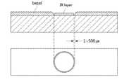
- Korean Patent Laid-Open Publication No. 10-2014-0003046discloses, as shown in FIG. 1 , a method for printing a proximity sensor coating layer of a mobile device, i.e., a technique screen printing an IR layer (transmitting IR of the proximity sensor, blocking visible light) on a bezel layer (decoration layer, BM layer) and printing a transparent coating layer for protecting the IR layer thereon.
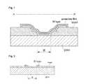
- Korean Patent Laid-Open Publication No. 10-2013-0063570discloses, as shown in FIG. 2 , a technique for preventing discoloration and cracks of an IR ink layer, which can be generated when depositing an electrode on the rear side of a window, by manufacturing the IR ink layer in the form of a tape and adhering thereof on the rear side of the transparent window.
- forming of a bezel layer and an infrared-transmissive layeris absolutely necessary process when manufacturing a touch panel cover glass, and process cost may be reduced if the forming process is completely at a time.
- the conventional processsuch as screen printing has a problem that this technique cannot print the two layers at the same time, and also there is a problem that print quality and material characteristics may become worse if different inks are mixed each other. Thus, there is an urgent need of an improvement over the problem.
- the present inventionhas been made keeping in mind the above problems in the related art, and an object of the present invention is to provide a method for printing a touch panel cover glass which can print a touch panel cover glass through only one process by simultaneously printing a bezel layer and an infrared-transmissive layer, using two or more inkjet heads, so as to print two or more inks at the desire location, respectively.
- the present inventionprovides a method for printing touch panel cover glass comprising the steps of: a) inkjet-printing both black ink for a bezel and infrared-transmissive ink on a glass by using two or more inkjet heads; and b) forming a bezel layer and an infrared-transmissive layer by curing the substrate, wherein a gap between the inkjet-printed black ink for a bezel and infrared-transmissive ink printed in the step a) is 1 ⁇ m to 500 ⁇ m.
- the present inventionprovides a touch panel cover glass wherein on a glass, a black ink layer for a bezel and an infrared-transmissive ink layer are inkjet-printed on the same plane, and a gap between the inkjet-printed black ink layer for a bezel and infrared-transmissive ink layer is 1 ⁇ m to 500 ⁇ m.
- the present inventionprovides a touch panel comprising the touch panel cover glass.
- the present inventionprovides a display substrate comprising the touch panel.
- a touch panel cover glasscan be manufactured through only one process by simultaneously printing a bezel layer and an infrared-transmissive layer, using two or more inkjet heads, so as to print two or more inks at the desire location, respectively. Therefore, there are advantages that entire process cost can be reduced and also a touch panel with high reliability can be manufactured.
- FIG. 1is a drawing showing a structure of a touch panel cover glass according to the conventional technique.
- FIG. 2is a drawing showing a structure of a touch panel cover glass according to the conventional technique.
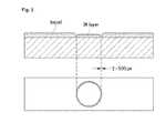
- FIG. 3is a drawing showing a structure of a touch panel cover glass according to the present invention.
- the method for printing a touch panel cover glassis characterized by comprising the steps of: a) inkjet-printing both black ink for a bezel and infrared-transmissive ink on a glass by using two or more inkjet heads; and b) forming a bezel layer and an infrared-transmissive layer by curing the substrate, wherein a gap between the inkjet-printed black ink for a bezel and infrared-transmissive ink printed in the step a) is 1 ⁇ m to 500 ⁇ m.
- both the black ink for a bezel and the infrared-transmissive inkare simultaneously inkjet-printed on a glass by using two or more inkjet heads.
- both the black ink for a bezel and the infrared-transmissive inkare simultaneously inkjet-printed on the glass.
- the glassmay be any one used in the art without particular limitation.
- the black ink for a bezelmay be any one used in the art without particular limitation, and preferably, it may be carbon black or titanium black having composition of a black pigment, an oligomer, a multifunctional monomer, a 1- to 3-functional monomers, an adhesive enhancer, a polymerization inhibitor, a surfactant and the like. Further, the black ink for a bezel may be one which can form pattern by an inkjet method, and has the viscosity of 1 cP to 50 cP and the surface tension of 18 N/m to 40 N/m at a room temperature (25° C.).
- the infrared-transmissive inkmay be any one used in the art without particular limitation, and preferably, it may be lactam black or a perylene black having high infrared transmissivity, which has composition of a black pigment, an oligomer, a multifunctional monomer, a 1- to 3-functional monomers, an adhesive enhancer, a polymerization inhibitor, a surfactant and the like. Further, the infrared-transmissive ink may be one which can form pattern by an inkjet method, and has the viscosity of 1 cP to 50 cP and the surface tension of 18 N/m to 40 N/m at a room temperature (25° C.).
- the method for printing a touch panel cover glass according to the present inventionmay use two or more inkjet heads in order to use two or more kinds of ink as mentioned above, and each inkjet head prints out only the color set on an image file.
- each of the inkjet headssimultaneously prints different ink.
- print qualitybecomes poor because the inks are mixed in the boundary between the inks, and in particular, characteristics of the infrared-transmissive layer (IR layer) become worse.
- the gap between the inkjet-printed black ink for a bezel and infrared-transmissive inkcan be set to 1 ⁇ m to 500 ⁇ m, and more preferably, the gap between the inkjet-printed black ink for a bezel and infrared-transmissive ink can be set to 1 ⁇ m to 100 ⁇ m.
- the gap between the inkjet-printed black ink for a bezel and infrared-transmissive inkis less than 1 ⁇ m, there may be a problems that print quality is deteriorated as the two different inks are mixed, and if the gap between the inkjet-printed black ink for a bezel and infrared-transmissive ink is more than 500 ⁇ m, there may be a problem that the infrared sensor is malfunctioned because visible light is entered through a unprinted part.
- the substrateis cured in the step b) to form the bezel layer and the infrared-transmissive layer.
- the curing methodmay preferably be an ultraviolet (UV) curing or heat curing method without particular limitation.
- UVultraviolet
- UV having the intensity of 1000 mJ/cm 2 to 20000 mJ/cm 2may preferably be irradiated without particular limitation.
- an oven or hat platemay preferably be used for heat curing without particular limitation.
- the heat curingmay be conducted at a condition of 150° C. to 220° C. and 10 min to 30 min without particular limitation.
- the thickness of the bezel layer cured as mentioned abovemay be 2 ⁇ m to 10 ⁇ m, and it may be 4 ⁇ m to 6 ⁇ m, if necessary.
- the optical density of the cured bezel layermay be 4 to 6, and it may be 4.5 to 5.5, if necessary. In this case, there is an advantage of excellent shielding characteristic by bezel pattern. If the optical density is higher than 6, it may cause deterioration of the UV curing sensitivity, and it may be difficult to form pattern due to the increased amount of shielding material added to realize the optical density.
- the cured bezelmay have the surface hardness of 4H or higher, the adhesive force of 5 B and the like those are required for the bezel performance.
- the thickness of the infrared-transmissive layer cured as mentioned abovemay be 2 ⁇ m to 10 ⁇ m, and it may be 4 ⁇ m to 6 ⁇ m, if necessary.
- the infrared-transmissive layer cured like thishas an advantage of maintaining the transmissivity in an infrared wavelength region (850 nm to 940 nm at 80% or higher (for example, the transmissivity at 850 nm is 82%, and the transmissivity at 940 nm is 83%), and the transmissivity in a visible light wavelength region (550 nm) at 20%.
- FIG. 3shows a touch panel cover glass according to the printing method of the present invention.
- the bezel layeris printed (inkjet) and at the same time the IR layer is printed (inkjet), and then the layers are cure.
- the bezel layeris printed (inkjet) and at the same time the IR layer is printed (inkjet), and then the layers are cure.
- a constant gapis formed between the black ink layer for a bezel and the infrared-transmissive ink layer.
- the gap between the black ink layer for a bezel and the infrared-transmissive ink layer inkjet-printed on the same plane of the glassmay be limited from 1 ⁇ m to 500 ⁇ m, and more preferably, the gap between the inkjet-printed black ink layer for a bezel and infrared-transmissive ink layer may be 1 ⁇ m to 100 ⁇ m.
- the gap between the inkjet-printed black ink layer for a bezel and infrared-transmissive ink layeris narrow than 1 ⁇ m, there may be a problem that print quality becomes poor because the two different inks are mixed each other, and if the gap between the inkjet-printed black ink layer for a bezel and infrared-transmissive ink layer is wider than 500 ⁇ m, there may be a problem of malfunction of the infrared sensor because visible light is entered through the unprinted part.
- the thickness of the bezel layer of the touch panel cover glass according to the present inventionmay be 2 ⁇ m to 10 ⁇ m, and it may be 4 ⁇ m to 6 ⁇ m, if necessary.
- the optical density of the bezel layer of the touch panel cover glass according to the present inventionmay be 4 to 6, and it may be 4.5 to 5, if necessary. In the case, there is an advantage of excellent shielding characteristic by bezel pattern. If the optical density is higher than 6, it may cause deterioration of the UV curing sensitivity, and it may be difficult to form pattern due to the increased amount of shielding material added to realize the optical density.
- bezel of the touch panel cover glass according to the present inventionmay show the performance required for bezel such as the surface hardness of 4H or higher, the adhesive force of 5 B and the like.
- the thickness of the infrared-transmissive layer of the touch panel cover glass according to the present inventionmay be 2 ⁇ m to 10 ⁇ m, and it may be 4 ⁇ m to 6 ⁇ m, if necessary.
- the infrared-transmissive layer cured like thishas an advantage of maintaining the transmissivity in an infrared wavelength region (850 nm to 940 nm) at 80% or higher (for example, the transmissivity at 850 nm is 82%, and the transmissivity at 940 nm is 83%), and the transmissivity in a visible light wavelength region (550 nm) at 20%.
- touch panel cover glass according to the present inventionmay be applied to a touch panel used in the art.
- touch panel according to the present inventionmay be applied to various display substrates by being combined with a liquid crystal module.
- a pigment dispersioncarbon black 30 wt %, acryl-based dispersant 6 wt %, HPNDA 64 wt %), 10 wt % of DPHA as a multifunctional monomer, 18 wt % of 2-HEA as a monofunctional monomer, 3 wt % of an adhesive enhancer KBM-403, 2 wt % of an epoxy binder (PD-7610, Almatex), 5 wt % of Irgacure 907 as a photo-initiator, 2 wt % of ITX as a photo-initiator, 0.05 wt % of a polymerization inhibitor, and 0.05 wt % of a surfactant BYK-307 are mixed, and then the mixture was stirred for 6 hours to manufacture a black ink composition for a bezel.
- a pigment dispersioncarbon black 30 wt %, acryl-based dispersant 6 wt %, HPNDA 64 wt %
- the black ink composition for a bezel of the ink composition 1 and the infrared-transmissive ink composition of the ink composition 2were inkjet-printed on a glass (width: 70 mm, length: 120 mm, and height: 0.5 ⁇ m) to the thickness of 5 ⁇ m to manufacture a sample having a black ink layer for a bezel and an infrared-transmissive ink layer.
- An image gap between the black ink layer for a bezel and the infrared-transmissive ink layerwas 1 ⁇ m, and the sample was UV cured using a UV LED lamp of 395 nm wavelength. In order to enhance the adhesive force, the cured sample was heated at 200° C. for 15 min to manufacture a cover glass.
- Example 1The procedure of Example 1 was repeated except for forming the image gap between the black ink layer for a bezel and the infrared-transmissive ink layer at 10 ⁇ m to manufacture a cover glass.
- Example 1The procedure of Example 1 was repeated except for forming the image gap between the black ink layer for a bezel and the infrared-transmissive ink layer at 100 ⁇ m to manufacture a cover glass.
- Example 1The procedure of Example 1 was repeated except for forming the image gap between the black ink layer for a bezel and the infrared-transmissive ink layer at 400 ⁇ m to manufacture a cover glass.
- Example 1The procedure of Example 1 was repeated except for forming the image gap between the black ink layer for a bezel and the infrared-transmissive ink layer at 0 ⁇ m to manufacture a cover glass.
- Example 1The procedure of Example 1 was repeated except for forming the image gap between the black ink layer for a bezel and the infrared-transmissive ink layer at 500 ⁇ m to manufacture a cover glass.
- Example 1The procedure of Example 1 was repeated except for forming the image gap between the black ink layer for a bezel and the infrared-transmissive ink layer at 600 ⁇ m to manufacture a cover glass.
- the infrared sensor performancewas measured by a light proximity sensor module and whether the sensor is normally operated or not when the light emitted from an IR LED is reflected and then entered into the sensor.
- the print qualitywas observed under a microscope, and whether the two printed layers are overlapped or not was checked.
- the surface hardnesswas measured using a pencil hardness tester under conditions of load of 1 kg, scratch angle of 45 degree(°) and rate of 3 mm/s (Standard: ASTM D3363), and the adhesive force was measured by conducting cross cut test and evaluated from 0 B to 5 B (Standard: ASTM D3002, D3359).
- touch panel cover glasses of Example 1 to Example 4 manufactured by the printing method of the present inventionhad good print quality and also had excellent infrared sensor performance. Further, it can be confirmed that the touch panel cover glasses manufactured by the printing method of the present invention also had excellent surface hardness and adhesive force.
- Comparative Example 1 without image gaphad a problem of bad print quality as the inks were mixed each other, and Comparative Examples 1 and 2 with too wide image gap had a problem of poor infrared sensor performance because visible light was transmitted through the infrared-transmissive ink layer and the light emitted from the light emitting part (IR LED) of the infrared sensor was not properly recognized at the light receiving part (sensor).
- IR LEDlight emitting part
Landscapes
- Engineering & Computer Science (AREA)
- Physics & Mathematics (AREA)
- Theoretical Computer Science (AREA)
- General Engineering & Computer Science (AREA)
- General Physics & Mathematics (AREA)
- Human Computer Interaction (AREA)
- Optics & Photonics (AREA)
- Health & Medical Sciences (AREA)
- Toxicology (AREA)
- Ink Jet (AREA)
- Position Input By Displaying (AREA)
- Laminated Bodies (AREA)
- Application Of Or Painting With Fluid Materials (AREA)
Abstract
Description
- The present application claims the benefit of priority to Korean Patent Application No. 10-2015-0167978, filed on Nov. 27, 2015, which is incorporated herein by reference in its entirety for all purpose.
- The present invention relates to method for printing a touch panel cover glass and a touch panel cover glass manufactured by using the same. More specifically, it relates to a method for printing a touch panel cover glass, which can manufacture a touch panel cover glass through only one process, by controlling a gap between an ink layer for a bezel and an infrared-transmissive ink layer on a touch panel cover glass by an inkjet-printing method using two inkjet heads, and a touch panel cover glass manufactured by using the same.
- Mobile devices including smart phones have become necessities to all modern people, and such mobile devices are developing day by day in their originality or convenience. However, along this growth trend, there are many problems to be solved, and studies to solve the problems have constantly continued. Among the problems, in the process manufacturing a touch panel of the mobile device, transparent electrode pattern was implemented on a display region of the touch panel by forming a bezel and an infrared (Infrared Ray; IR)-transmissive layer for a proximity sensor of the touch panel, and at this time, there was a problem of high process cost because a layer-formation process was needed two or more times to form each layer.
- For example, Korean Patent Laid-Open Publication No. 10-2014-0003046 discloses, as shown in
FIG. 1 , a method for printing a proximity sensor coating layer of a mobile device, i.e., a technique screen printing an IR layer (transmitting IR of the proximity sensor, blocking visible light) on a bezel layer (decoration layer, BM layer) and printing a transparent coating layer for protecting the IR layer thereon. - Further, Korean Patent Laid-Open Publication No. 10-2013-0063570 discloses, as shown in
FIG. 2 , a technique for preventing discoloration and cracks of an IR ink layer, which can be generated when depositing an electrode on the rear side of a window, by manufacturing the IR ink layer in the form of a tape and adhering thereof on the rear side of the transparent window. - However, such conventional techniques needs two or more processes, for example, manufacturing the bezel layer and manufacturing the IR layer for preventing malfunction of the infrared sensor (proximity sensor) thereon. Thus, there is a problem of high process cost.
- Thus, forming of a bezel layer and an infrared-transmissive layer (IR layer) is absolutely necessary process when manufacturing a touch panel cover glass, and process cost may be reduced if the forming process is completely at a time. However, the conventional process such as screen printing has a problem that this technique cannot print the two layers at the same time, and also there is a problem that print quality and material characteristics may become worse if different inks are mixed each other. Thus, there is an urgent need of an improvement over the problem.
- The present invention has been made keeping in mind the above problems in the related art, and an object of the present invention is to provide a method for printing a touch panel cover glass which can print a touch panel cover glass through only one process by simultaneously printing a bezel layer and an infrared-transmissive layer, using two or more inkjet heads, so as to print two or more inks at the desire location, respectively.
- In order to achieve the above object, the present invention provides a method for printing touch panel cover glass comprising the steps of: a) inkjet-printing both black ink for a bezel and infrared-transmissive ink on a glass by using two or more inkjet heads; and b) forming a bezel layer and an infrared-transmissive layer by curing the substrate, wherein a gap between the inkjet-printed black ink for a bezel and infrared-transmissive ink printed in the step a) is 1 μm to 500 μm.
- Further, the present invention provides a touch panel cover glass wherein on a glass, a black ink layer for a bezel and an infrared-transmissive ink layer are inkjet-printed on the same plane, and a gap between the inkjet-printed black ink layer for a bezel and infrared-transmissive ink layer is 1 μm to 500 μm.
- Further, the present invention provides a touch panel comprising the touch panel cover glass.
- Further, the present invention provides a display substrate comprising the touch panel.
- According to the method for printing a touch panel cover glass of the present invention, a touch panel cover glass can be manufactured through only one process by simultaneously printing a bezel layer and an infrared-transmissive layer, using two or more inkjet heads, so as to print two or more inks at the desire location, respectively. Therefore, there are advantages that entire process cost can be reduced and also a touch panel with high reliability can be manufactured.
FIG. 1 is a drawing showing a structure of a touch panel cover glass according to the conventional technique.FIG. 2 is a drawing showing a structure of a touch panel cover glass according to the conventional technique.FIG. 3 is a drawing showing a structure of a touch panel cover glass according to the present invention.- Hereinafter, the present invention will be described in detail.
- The method for printing a touch panel cover glass according to the present invention is characterized by comprising the steps of: a) inkjet-printing both black ink for a bezel and infrared-transmissive ink on a glass by using two or more inkjet heads; and b) forming a bezel layer and an infrared-transmissive layer by curing the substrate, wherein a gap between the inkjet-printed black ink for a bezel and infrared-transmissive ink printed in the step a) is 1 μm to 500 μm.
- First, in the step a) of the method for printing a touch panel cover glass according to the present invention, both the black ink for a bezel and the infrared-transmissive ink are simultaneously inkjet-printed on a glass by using two or more inkjet heads.
- Referring to
FIG. 3 , in the step a), both the black ink for a bezel and the infrared-transmissive ink are simultaneously inkjet-printed on the glass. - The glass may be any one used in the art without particular limitation.
- The black ink for a bezel may be any one used in the art without particular limitation, and preferably, it may be carbon black or titanium black having composition of a black pigment, an oligomer, a multifunctional monomer, a 1- to 3-functional monomers, an adhesive enhancer, a polymerization inhibitor, a surfactant and the like. Further, the black ink for a bezel may be one which can form pattern by an inkjet method, and has the viscosity of 1 cP to 50 cP and the surface tension of 18 N/m to 40 N/m at a room temperature (25° C.).
- The infrared-transmissive ink may be any one used in the art without particular limitation, and preferably, it may be lactam black or a perylene black having high infrared transmissivity, which has composition of a black pigment, an oligomer, a multifunctional monomer, a 1- to 3-functional monomers, an adhesive enhancer, a polymerization inhibitor, a surfactant and the like. Further, the infrared-transmissive ink may be one which can form pattern by an inkjet method, and has the viscosity of 1 cP to 50 cP and the surface tension of 18 N/m to 40 N/m at a room temperature (25° C.).
- The method for printing a touch panel cover glass according to the present invention may use two or more inkjet heads in order to use two or more kinds of ink as mentioned above, and each inkjet head prints out only the color set on an image file.
- When inkjet-printing an image containing information about two colors of the bezel layer and the infrared-transmissive layer located at different places by using the two or more inkjet heads, each of the inkjet heads simultaneously prints different ink. However, as the different inks are printed at the same time, print quality becomes poor because the inks are mixed in the boundary between the inks, and in particular, characteristics of the infrared-transmissive layer (IR layer) become worse.
- For this, in order to develop a process method having excellent print quality and characteristics because the method can simultaneously print two different inks but the inks are not mixed each other, in the step a), the gap between the inkjet-printed black ink for a bezel and infrared-transmissive ink can be set to 1 μm to 500 μm, and more preferably, the gap between the inkjet-printed black ink for a bezel and infrared-transmissive ink can be set to 1 μm to 100 μm. If the gap between the inkjet-printed black ink for a bezel and infrared-transmissive ink is less than 1 μm, there may be a problems that print quality is deteriorated as the two different inks are mixed, and if the gap between the inkjet-printed black ink for a bezel and infrared-transmissive ink is more than 500 μm, there may be a problem that the infrared sensor is malfunctioned because visible light is entered through a unprinted part.
- In the present invention, after printing the bezel layer and the infrared-transmissive layer through one process as mentioned above, the substrate is cured in the step b) to form the bezel layer and the infrared-transmissive layer.
- The curing method may preferably be an ultraviolet (UV) curing or heat curing method without particular limitation.
- First, when curing by irradiating UV, UV having the intensity of 1000 mJ/cm2to 20000 mJ/cm2may preferably be irradiated without particular limitation.
- Further, when curing by heating, an oven or hat plate may preferably be used for heat curing without particular limitation. The heat curing may be conducted at a condition of 150° C. to 220° C. and 10 min to 30 min without particular limitation.
- The thickness of the bezel layer cured as mentioned above may be 2 μm to 10 μm, and it may be 4 μm to 6 μm, if necessary.
- The optical density of the cured bezel layer may be 4 to 6, and it may be 4.5 to 5.5, if necessary. In this case, there is an advantage of excellent shielding characteristic by bezel pattern. If the optical density is higher than 6, it may cause deterioration of the UV curing sensitivity, and it may be difficult to form pattern due to the increased amount of shielding material added to realize the optical density.
- Further, the cured bezel may have the surface hardness of 4H or higher, the adhesive force of5B and the like those are required for the bezel performance.
- Further, the thickness of the infrared-transmissive layer cured as mentioned above may be 2 μm to 10 μm, and it may be 4 μm to 6 μm, if necessary.
- The infrared-transmissive layer cured like this has an advantage of maintaining the transmissivity in an infrared wavelength region (850 nm to 940 nm at 80% or higher (for example, the transmissivity at 850 nm is 82%, and the transmissivity at 940 nm is 83%), and the transmissivity in a visible light wavelength region (550 nm) at 20%.
FIG. 3 shows a touch panel cover glass according to the printing method of the present invention. As shown inFIG. 3 , the bezel layer is printed (inkjet) and at the same time the IR layer is printed (inkjet), and then the layers are cure. Thus, it is possible to reduce process time and cost spent for printing the bezel layer and the IR layer.- In order to develop a touch panel cover glass having excellent print quality and characteristics because two different inks are not mixed each other while printing with the two different inks, as illustrated in
FIG. 3 , a constant gap is formed between the black ink layer for a bezel and the infrared-transmissive ink layer. - Thus, in the touch panel cover glass of the present invention, the gap between the black ink layer for a bezel and the infrared-transmissive ink layer inkjet-printed on the same plane of the glass may be limited from 1 μm to 500 μm, and more preferably, the gap between the inkjet-printed black ink layer for a bezel and infrared-transmissive ink layer may be 1 μm to 100 μm. If the gap between the inkjet-printed black ink layer for a bezel and infrared-transmissive ink layer is narrow than 1 μm, there may be a problem that print quality becomes poor because the two different inks are mixed each other, and if the gap between the inkjet-printed black ink layer for a bezel and infrared-transmissive ink layer is wider than 500 μm, there may be a problem of malfunction of the infrared sensor because visible light is entered through the unprinted part.
- Further, the thickness of the bezel layer of the touch panel cover glass according to the present invention may be 2 μm to 10 μm, and it may be 4 μm to 6 μm, if necessary.
- Further, the optical density of the bezel layer of the touch panel cover glass according to the present invention may be 4 to 6, and it may be 4.5 to 5, if necessary. In the case, there is an advantage of excellent shielding characteristic by bezel pattern. If the optical density is higher than 6, it may cause deterioration of the UV curing sensitivity, and it may be difficult to form pattern due to the increased amount of shielding material added to realize the optical density.
- Further, the bezel of the touch panel cover glass according to the present invention may show the performance required for bezel such as the surface hardness of 4H or higher, the adhesive force of5B and the like.
- Further, the thickness of the infrared-transmissive layer of the touch panel cover glass according to the present invention may be 2 μm to 10 μm, and it may be 4 μm to 6 μm, if necessary.
- The infrared-transmissive layer cured like this has an advantage of maintaining the transmissivity in an infrared wavelength region (850 nm to 940 nm) at 80% or higher (for example, the transmissivity at 850 nm is 82%, and the transmissivity at 940 nm is 83%), and the transmissivity in a visible light wavelength region (550 nm) at 20%.
- Further, the touch panel cover glass according to the present invention may be applied to a touch panel used in the art.
- Further, the touch panel according to the present invention may be applied to various display substrates by being combined with a liquid crystal module.
- The present invention will be explained in detail with reference to the following examples, including test examples. However, these examples are provided for illustrative purposes only and are not intended to limit the scope of the invention.
- Base on the total weight of the whole ink composition, 60 wt % of a pigment dispersion (carbon black 30 wt %, acryl-based dispersant 6 wt %, HPNDA 64 wt %), 10 wt % of DPHA as a multifunctional monomer, 18 wt % of 2-HEA as a monofunctional monomer, 3 wt % of an adhesive enhancer KBM-403, 2 wt % of an epoxy binder (PD-7610, Almatex), 5 wt % of Irgacure 907 as a photo-initiator, 2 wt % of ITX as a photo-initiator, 0.05 wt % of a polymerization inhibitor, and 0.05 wt % of a surfactant BYK-307 are mixed, and then the mixture was stirred for 6 hours to manufacture a black ink composition for a bezel.
- Base on the total weight of the whole ink composition, 25 wt % of a pigment dispersion (lactam black 20 wt %, acryl-based dispersant 4 wt %, HPNDA 76 wt %), 12 wt % of DPHA as a multifunctional monomer, 25 wt % of TMPTA as a 3-functional monomer, 23.5 wt % of 2-HEA as a monofunctional monomer, 5 wt % of an adhesive enhancer KBM-403, 2 wt % of an epoxy binder (PD-7610, Almatex), 5 wt % of Irgacure 907 as a photo-initiator, 2 wt % of ITX as a photo-initiator, 0.05 wt % of a polymerization inhibitor, and 0.5 wt % of a surfactant RS-75 are mixed, and then the mixture was stirred for 6 hours to manufacture an infrared-transmissive ink composition.
- Using 2 inkjet heads, the black ink composition for a bezel of the ink composition 1 and the infrared-transmissive ink composition of the ink composition 2 were inkjet-printed on a glass (width: 70 mm, length: 120 mm, and height: 0.5 μm) to the thickness of 5 μm to manufacture a sample having a black ink layer for a bezel and an infrared-transmissive ink layer. An image gap between the black ink layer for a bezel and the infrared-transmissive ink layer was 1 μm, and the sample was UV cured using a UV LED lamp of 395 nm wavelength. In order to enhance the adhesive force, the cured sample was heated at 200° C. for 15 min to manufacture a cover glass.
- The procedure of Example 1 was repeated except for forming the image gap between the black ink layer for a bezel and the infrared-transmissive ink layer at 10 μm to manufacture a cover glass.
- The procedure of Example 1 was repeated except for forming the image gap between the black ink layer for a bezel and the infrared-transmissive ink layer at 100 μm to manufacture a cover glass.
- The procedure of Example 1 was repeated except for forming the image gap between the black ink layer for a bezel and the infrared-transmissive ink layer at 400 μm to manufacture a cover glass.
- The procedure of Example 1 was repeated except for forming the image gap between the black ink layer for a bezel and the infrared-transmissive ink layer at 0 μm to manufacture a cover glass.
- The procedure of Example 1 was repeated except for forming the image gap between the black ink layer for a bezel and the infrared-transmissive ink layer at 500 μm to manufacture a cover glass.
- The procedure of Example 1 was repeated except for forming the image gap between the black ink layer for a bezel and the infrared-transmissive ink layer at 600 μm to manufacture a cover glass.
- For the cover glasses manufactured in Example 1 to Example 4 and Comparative Example 1 to Comparative Example 3, the infrared sensor performance, the print quality, the surface hardness and the adhesive force were tested as follows, and the results are shown in the following Table 1.
- The infrared sensor performance was measured by a light proximity sensor module and whether the sensor is normally operated or not when the light emitted from an IR LED is reflected and then entered into the sensor. The print quality was observed under a microscope, and whether the two printed layers are overlapped or not was checked.
- Further, the surface hardness was measured using a pencil hardness tester under conditions of load of 1 kg, scratch angle of 45 degree(°) and rate of 3 mm/s (Standard: ASTM D3363), and the adhesive force was measured by conducting cross cut test and evaluated from 0 B to 5 B (Standard: ASTM D3002, D3359).
TABLE 1 Exam. Exam. Exam. Exam. Comp. Comp. Comp. 1 2 3 4 Exam. 1 Exam. 2 Exam. 3 Image 1 10 100 400 0 500 600 gap (μm) Print OK OK OK OK NG OK OK quality Infrared OK OK OK OK OK NG NG sensor performance Surface 4H 4H 4H 4H 4H 4H 4H hardness Adhesive 5B 5B 5B 5B 5B 5B 5B force - It can be confirmed that the touch panel cover glasses of Example 1 to Example 4 manufactured by the printing method of the present invention had good print quality and also had excellent infrared sensor performance. Further, it can be confirmed that the touch panel cover glasses manufactured by the printing method of the present invention also had excellent surface hardness and adhesive force.
- However, Comparative Example 1 without image gap had a problem of bad print quality as the inks were mixed each other, and Comparative Examples 1 and 2 with too wide image gap had a problem of poor infrared sensor performance because visible light was transmitted through the infrared-transmissive ink layer and the light emitted from the light emitting part (IR LED) of the infrared sensor was not properly recognized at the light receiving part (sensor).
Claims (26)
Applications Claiming Priority (3)
| Application Number | Priority Date | Filing Date | Title |
|---|---|---|---|
| KR10-2015-0167978 | 2015-11-27 | ||
| KR1020150167978AKR101952735B1 (en) | 2015-11-27 | 2015-11-27 | A printing method of a cover glass for touch panel and cover glass for touch panel manufactured by the same |
| PCT/KR2016/013809WO2017091052A1 (en) | 2015-11-27 | 2016-11-28 | Method for printing touch panel cover glass and touch panel cover glass manufactured by using same |
Publications (2)
| Publication Number | Publication Date |
|---|---|
| US20180275787A1true US20180275787A1 (en) | 2018-09-27 |
| US10877603B2 US10877603B2 (en) | 2020-12-29 |
Family
ID=58763422
Family Applications (1)
| Application Number | Title | Priority Date | Filing Date |
|---|---|---|---|
| US15/757,215Active2037-01-21US10877603B2 (en) | 2015-11-27 | 2016-11-28 | Method for printing touch panel cover glass and touch panel cover glass manufactured by using same |
Country Status (4)
| Country | Link |
|---|---|
| US (1) | US10877603B2 (en) |
| KR (1) | KR101952735B1 (en) |
| CN (1) | CN108139827B (en) |
| WO (1) | WO2017091052A1 (en) |
Cited By (2)
| Publication number | Priority date | Publication date | Assignee | Title |
|---|---|---|---|---|
| US10934443B2 (en) | 2017-08-18 | 2021-03-02 | Lg Chem, Ltd. | Infrared transmitting ink composition for ink jet, method for forming bezel pattern by using same, bezel pattern formed thereby, and display substrate comprising same |
| CN115033093A (en)* | 2021-03-05 | 2022-09-09 | 江苏通祐视觉科技有限公司 | Infrared Gesture Control Panel |
Families Citing this family (3)
| Publication number | Priority date | Publication date | Assignee | Title |
|---|---|---|---|---|
| KR102528525B1 (en)* | 2018-01-10 | 2023-05-03 | 삼성디스플레이 주식회사 | Display device |
| JP2019191340A (en)* | 2018-04-24 | 2019-10-31 | Agc株式会社 | Transparent plate with light shielding layer |
| CN110413151B (en)* | 2019-07-16 | 2020-10-16 | 惠州市华星光电技术有限公司 | Touch display panel and touch display device |
Citations (11)
| Publication number | Priority date | Publication date | Assignee | Title |
|---|---|---|---|---|
| JPH07140314A (en)* | 1993-11-16 | 1995-06-02 | Mitsumura Insatsu Kk | Color filter forming method |
| US5514502A (en)* | 1993-08-16 | 1996-05-07 | Fuji Photo Film Co., Ltd. | Photopolymerizable composition, color filter, and production of color filter |
| US20020130913A1 (en)* | 2001-03-13 | 2002-09-19 | Olympus Optical Co., Ltd. | Printer |
| US20080158173A1 (en)* | 2007-01-03 | 2008-07-03 | Apple Computer, Inc. | Multi-touch surface stackup arrangement |
| US20120170284A1 (en)* | 2010-12-30 | 2012-07-05 | Anna-Katrina Shedletsky | Diffuser and filter structures for light sensors |
| US20120295665A1 (en)* | 2011-05-19 | 2012-11-22 | Apple Inc. | Proximity and ambient light sensor with improved smudge rejection |
| WO2013176517A1 (en)* | 2012-05-25 | 2013-11-28 | 주식회사 엘지화학 | Photosensitive resin composition, pattern formed using same and display panel comprising same |
| WO2013179237A1 (en)* | 2012-06-01 | 2013-12-05 | Basf Se | Black colorant mixture |
| KR20140047773A (en)* | 2012-10-12 | 2014-04-23 | 주식회사 엘지화학 | Ink composition improved wear resistance and electronic device using the same |
| KR20140065155A (en)* | 2012-11-21 | 2014-05-29 | 김영수 | Touch screen panel protection sheet and manufacturing method thereof |
| WO2015178447A1 (en)* | 2014-05-23 | 2015-11-26 | Dic株式会社 | Image display device and oriented material used in same |
Family Cites Families (9)
| Publication number | Priority date | Publication date | Assignee | Title |
|---|---|---|---|---|
| JP2007140314A (en) | 2005-11-22 | 2007-06-07 | Nidec Copal Corp | Device for automatically focusing digital camera |
| JP2009021552A (en)* | 2007-06-14 | 2009-01-29 | Seiko Epson Corp | Contact hole forming method, conductive post forming method, wiring pattern forming method, multilayer wiring board manufacturing method, and electronic device manufacturing method |
| US8324578B2 (en)* | 2008-09-30 | 2012-12-04 | Apple Inc. | Hidden sensors in an electronic device |
| KR20130063570A (en) | 2011-12-07 | 2013-06-17 | 엘지전자 주식회사 | Mobile terminal and method for manufacturing the same |
| CN103257470A (en)* | 2012-02-17 | 2013-08-21 | 群康科技(深圳)有限公司 | Screen device of display, method for manufacturing screen device and touch display device |
| KR20140003046A (en) | 2012-06-29 | 2014-01-09 | 엘지이노텍 주식회사 | Touch window and fabricating method of the same, and lcd using the same |
| EP2728387A1 (en)* | 2012-10-31 | 2014-05-07 | ams AG | Proximity sensor module |
| CN203520350U (en)* | 2013-09-30 | 2014-04-02 | 金龙机电(东莞)有限公司 | A production line of ultra-thin touch screen |
| TW201516793A (en)* | 2013-10-28 | 2015-05-01 | Wintek Corp | Touch panel and cover plate structure |
- 2015
- 2015-11-27KRKR1020150167978Apatent/KR101952735B1/enactiveActive
- 2016
- 2016-11-28USUS15/757,215patent/US10877603B2/enactiveActive
- 2016-11-28WOPCT/KR2016/013809patent/WO2017091052A1/ennot_activeCeased
- 2016-11-28CNCN201680057739.3Apatent/CN108139827B/enactiveActive
Patent Citations (13)
| Publication number | Priority date | Publication date | Assignee | Title |
|---|---|---|---|---|
| US5514502A (en)* | 1993-08-16 | 1996-05-07 | Fuji Photo Film Co., Ltd. | Photopolymerizable composition, color filter, and production of color filter |
| JPH07140314A (en)* | 1993-11-16 | 1995-06-02 | Mitsumura Insatsu Kk | Color filter forming method |
| US20020130913A1 (en)* | 2001-03-13 | 2002-09-19 | Olympus Optical Co., Ltd. | Printer |
| US20080158173A1 (en)* | 2007-01-03 | 2008-07-03 | Apple Computer, Inc. | Multi-touch surface stackup arrangement |
| US20120170284A1 (en)* | 2010-12-30 | 2012-07-05 | Anna-Katrina Shedletsky | Diffuser and filter structures for light sensors |
| US20120295665A1 (en)* | 2011-05-19 | 2012-11-22 | Apple Inc. | Proximity and ambient light sensor with improved smudge rejection |
| WO2013176517A1 (en)* | 2012-05-25 | 2013-11-28 | 주식회사 엘지화학 | Photosensitive resin composition, pattern formed using same and display panel comprising same |
| US20150125789A1 (en)* | 2012-05-25 | 2015-05-07 | Lg Chem, Ltd. | Photosensitive resin composition, pattern formed using same and display panel comprising same |
| WO2013179237A1 (en)* | 2012-06-01 | 2013-12-05 | Basf Se | Black colorant mixture |
| KR20140047773A (en)* | 2012-10-12 | 2014-04-23 | 주식회사 엘지화학 | Ink composition improved wear resistance and electronic device using the same |
| KR20140065155A (en)* | 2012-11-21 | 2014-05-29 | 김영수 | Touch screen panel protection sheet and manufacturing method thereof |
| WO2015178447A1 (en)* | 2014-05-23 | 2015-11-26 | Dic株式会社 | Image display device and oriented material used in same |
| US20170205669A1 (en)* | 2014-05-23 | 2017-07-20 | Dic Corporation | Image display device and oriented material used in same |
Cited By (2)
| Publication number | Priority date | Publication date | Assignee | Title |
|---|---|---|---|---|
| US10934443B2 (en) | 2017-08-18 | 2021-03-02 | Lg Chem, Ltd. | Infrared transmitting ink composition for ink jet, method for forming bezel pattern by using same, bezel pattern formed thereby, and display substrate comprising same |
| CN115033093A (en)* | 2021-03-05 | 2022-09-09 | 江苏通祐视觉科技有限公司 | Infrared Gesture Control Panel |
Also Published As
| Publication number | Publication date |
|---|---|
| KR20170062314A (en) | 2017-06-07 |
| WO2017091052A1 (en) | 2017-06-01 |
| US10877603B2 (en) | 2020-12-29 |
| CN108139827A (en) | 2018-06-08 |
| KR101952735B1 (en) | 2019-02-27 |
| CN108139827B (en) | 2021-12-07 |
Similar Documents
| Publication | Publication Date | Title |
|---|---|---|
| US10877603B2 (en) | Method for printing touch panel cover glass and touch panel cover glass manufactured by using same | |
| KR102125597B1 (en) | An uv curable ink composition for bezel and a method for forming a bezel pattern using the same | |
| US10088611B2 (en) | Color filter forming substrate, method of manufacturing same and display device | |
| US8797637B2 (en) | Color display device for electronic paper, and process for production thereof | |
| US20090098308A1 (en) | Correction ink for micro defect of color pattern, color filter, method for correcting micro defect of color pattern, and process for producing ink | |
| KR101871565B1 (en) | Polarizer plate and display device comprising the same | |
| KR102067857B1 (en) | A method for forming a bezel pattern using inkjet printing | |
| TW201300466A (en) | Color material dispersion liquid, color resin composition for color filters, color filter, liquid crystal display device and organic light-emitting display device | |
| KR102214938B1 (en) | Manufacturing methode of integrated deco-film for touch window and integrated deco-film for touch window manufactured by the same | |
| KR101703166B1 (en) | Uv curable ink for inkjet, method for manufacturing a bezel using the same, a bezel pattern using the same method and dispaly panel comprising the bezel pattern | |
| KR20090014159A (en) | Colored resin composition and inkjet ink using the same | |
| KR20090069147A (en) | Light guide plate patterning of micro lens inkjet method using plasma pretreatment | |
| US9234108B1 (en) | LED curable ink system for multi colored sub-surface applications | |
| US20110288198A1 (en) | Uv curable ink for a plastic gazing system | |
| JP2012103472A (en) | Ink jet ink composition | |
| KR20170046692A (en) | Backlight systems containing downconversion film elements | |
| KR101997878B1 (en) | Uv-curable and infrared ray transmittance ink composition for inkjetting enhanced high temperature heat resistance | |
| KR102683664B1 (en) | Multi-functional sheet capable of diffusion and retroreflection, preparation method thereof and back light unit comprising the same | |
| KR102163360B1 (en) | Cellular phone decoration film and manufacturing method thereof | |
| KR102737423B1 (en) | Light Scattering Ink Composition, Color Filter and Display Device | |
| EP2833171B1 (en) | Method for producing a display color filter | |
| KR20100028834A (en) | Hard coating film with excellent color vision | |
| JP2017156411A (en) | Decorative member and organic electroluminescence element | |
| WO2016152344A1 (en) | Recording sheet for decorative lighting and method for producing same, image sheet for decorative lighting and method for producing same, and illuminated signboard | |
| JP2024087319A (en) | Low-reflectivity laminate and method for producing same |
Legal Events
| Date | Code | Title | Description |
|---|---|---|---|
| AS | Assignment | Owner name:LG CHEM, LTD., KOREA, REPUBLIC OF Free format text:ASSIGNMENT OF ASSIGNORS INTEREST;ASSIGNORS:YOO, JAE-HYUN;KIM, MI-KYOUNG;KIM, JOON-HYUNG;REEL/FRAME:045092/0685 Effective date:20180226 | |
| FEPP | Fee payment procedure | Free format text:ENTITY STATUS SET TO UNDISCOUNTED (ORIGINAL EVENT CODE: BIG.); ENTITY STATUS OF PATENT OWNER: LARGE ENTITY | |
| STPP | Information on status: patent application and granting procedure in general | Free format text:DOCKETED NEW CASE - READY FOR EXAMINATION | |
| STPP | Information on status: patent application and granting procedure in general | Free format text:NON FINAL ACTION MAILED | |
| STPP | Information on status: patent application and granting procedure in general | Free format text:RESPONSE TO NON-FINAL OFFICE ACTION ENTERED AND FORWARDED TO EXAMINER | |
| STPP | Information on status: patent application and granting procedure in general | Free format text:RESPONSE TO NON-FINAL OFFICE ACTION ENTERED AND FORWARDED TO EXAMINER | |
| STPP | Information on status: patent application and granting procedure in general | Free format text:FINAL REJECTION MAILED | |
| STPP | Information on status: patent application and granting procedure in general | Free format text:DOCKETED NEW CASE - READY FOR EXAMINATION | |
| STPP | Information on status: patent application and granting procedure in general | Free format text:AWAITING TC RESP., ISSUE FEE NOT PAID | |
| STPP | Information on status: patent application and granting procedure in general | Free format text:PUBLICATIONS -- ISSUE FEE PAYMENT RECEIVED | |
| STPP | Information on status: patent application and granting procedure in general | Free format text:AWAITING TC RESP, ISSUE FEE PAYMENT VERIFIED | |
| STCF | Information on status: patent grant | Free format text:PATENTED CASE | |
| MAFP | Maintenance fee payment | Free format text:PAYMENT OF MAINTENANCE FEE, 4TH YEAR, LARGE ENTITY (ORIGINAL EVENT CODE: M1551); ENTITY STATUS OF PATENT OWNER: LARGE ENTITY Year of fee payment:4 |