US20180190580A1 - Bonded structures with integrated passive component - Google Patents
Bonded structures with integrated passive componentDownload PDFInfo
- Publication number
- US20180190580A1 US20180190580A1US15/856,391US201715856391AUS2018190580A1US 20180190580 A1US20180190580 A1US 20180190580A1US 201715856391 AUS201715856391 AUS 201715856391AUS 2018190580 A1US2018190580 A1US 2018190580A1
- Authority
- US
- United States
- Prior art keywords
- capacitor
- insulating
- electronic component
- passive
- passive electronic
- Prior art date
- Legal status (The legal status is an assumption and is not a legal conclusion. Google has not performed a legal analysis and makes no representation as to the accuracy of the status listed.)
- Granted
Links
Images


Classifications
- H—ELECTRICITY
- H01—ELECTRIC ELEMENTS
- H01L—SEMICONDUCTOR DEVICES NOT COVERED BY CLASS H10
- H01L23/00—Details of semiconductor or other solid state devices
- H01L23/48—Arrangements for conducting electric current to or from the solid state body in operation, e.g. leads, terminal arrangements ; Selection of materials therefor
- H01L23/488—Arrangements for conducting electric current to or from the solid state body in operation, e.g. leads, terminal arrangements ; Selection of materials therefor consisting of soldered or bonded constructions
- H01L23/498—Leads, i.e. metallisations or lead-frames on insulating substrates, e.g. chip carriers
- H01L23/49838—Geometry or layout
- H—ELECTRICITY
- H01—ELECTRIC ELEMENTS
- H01L—SEMICONDUCTOR DEVICES NOT COVERED BY CLASS H10
- H01L23/00—Details of semiconductor or other solid state devices
- H01L23/58—Structural electrical arrangements for semiconductor devices not otherwise provided for, e.g. in combination with batteries
- H01L23/64—Impedance arrangements
- H01L23/642—Capacitive arrangements
- H—ELECTRICITY
- H01—ELECTRIC ELEMENTS
- H01G—CAPACITORS; CAPACITORS, RECTIFIERS, DETECTORS, SWITCHING DEVICES, LIGHT-SENSITIVE OR TEMPERATURE-SENSITIVE DEVICES OF THE ELECTROLYTIC TYPE
- H01G2/00—Details of capacitors not covered by a single one of groups H01G4/00-H01G11/00
- H01G2/02—Mountings
- H—ELECTRICITY
- H01—ELECTRIC ELEMENTS
- H01G—CAPACITORS; CAPACITORS, RECTIFIERS, DETECTORS, SWITCHING DEVICES, LIGHT-SENSITIVE OR TEMPERATURE-SENSITIVE DEVICES OF THE ELECTROLYTIC TYPE
- H01G4/00—Fixed capacitors; Processes of their manufacture
- H01G4/002—Details
- H01G4/018—Dielectrics
- H01G4/06—Solid dielectrics
- H01G4/08—Inorganic dielectrics
- H01G4/12—Ceramic dielectrics
- H01G4/1209—Ceramic dielectrics characterised by the ceramic dielectric material
- H01G4/1236—Ceramic dielectrics characterised by the ceramic dielectric material based on zirconium oxides or zirconates
- H01G4/1245—Ceramic dielectrics characterised by the ceramic dielectric material based on zirconium oxides or zirconates containing also titanates
- H—ELECTRICITY
- H01—ELECTRIC ELEMENTS
- H01G—CAPACITORS; CAPACITORS, RECTIFIERS, DETECTORS, SWITCHING DEVICES, LIGHT-SENSITIVE OR TEMPERATURE-SENSITIVE DEVICES OF THE ELECTROLYTIC TYPE
- H01G4/00—Fixed capacitors; Processes of their manufacture
- H01G4/002—Details
- H01G4/228—Terminals
- H—ELECTRICITY
- H01—ELECTRIC ELEMENTS
- H01G—CAPACITORS; CAPACITORS, RECTIFIERS, DETECTORS, SWITCHING DEVICES, LIGHT-SENSITIVE OR TEMPERATURE-SENSITIVE DEVICES OF THE ELECTROLYTIC TYPE
- H01G4/00—Fixed capacitors; Processes of their manufacture
- H01G4/30—Stacked capacitors
- H—ELECTRICITY
- H01—ELECTRIC ELEMENTS
- H01G—CAPACITORS; CAPACITORS, RECTIFIERS, DETECTORS, SWITCHING DEVICES, LIGHT-SENSITIVE OR TEMPERATURE-SENSITIVE DEVICES OF THE ELECTROLYTIC TYPE
- H01G4/00—Fixed capacitors; Processes of their manufacture
- H01G4/40—Structural combinations of fixed capacitors with other electric elements, the structure mainly consisting of a capacitor, e.g. RC combinations
- H—ELECTRICITY
- H01—ELECTRIC ELEMENTS
- H01L—SEMICONDUCTOR DEVICES NOT COVERED BY CLASS H10
- H01L23/00—Details of semiconductor or other solid state devices
- H01L23/34—Arrangements for cooling, heating, ventilating or temperature compensation ; Temperature sensing arrangements
- H01L23/36—Selection of materials, or shaping, to facilitate cooling or heating, e.g. heatsinks
- H—ELECTRICITY
- H01—ELECTRIC ELEMENTS
- H01L—SEMICONDUCTOR DEVICES NOT COVERED BY CLASS H10
- H01L23/00—Details of semiconductor or other solid state devices
- H01L23/48—Arrangements for conducting electric current to or from the solid state body in operation, e.g. leads, terminal arrangements ; Selection of materials therefor
- H01L23/482—Arrangements for conducting electric current to or from the solid state body in operation, e.g. leads, terminal arrangements ; Selection of materials therefor consisting of lead-in layers inseparably applied to the semiconductor body (electrodes)
- H01L23/485—Arrangements for conducting electric current to or from the solid state body in operation, e.g. leads, terminal arrangements ; Selection of materials therefor consisting of lead-in layers inseparably applied to the semiconductor body (electrodes) consisting of layered constructions comprising conductive layers and insulating layers, e.g. planar contacts
- H—ELECTRICITY
- H01—ELECTRIC ELEMENTS
- H01L—SEMICONDUCTOR DEVICES NOT COVERED BY CLASS H10
- H01L23/00—Details of semiconductor or other solid state devices
- H01L23/48—Arrangements for conducting electric current to or from the solid state body in operation, e.g. leads, terminal arrangements ; Selection of materials therefor
- H01L23/488—Arrangements for conducting electric current to or from the solid state body in operation, e.g. leads, terminal arrangements ; Selection of materials therefor consisting of soldered or bonded constructions
- H01L23/498—Leads, i.e. metallisations or lead-frames on insulating substrates, e.g. chip carriers
- H01L23/49822—Multilayer substrates
- H—ELECTRICITY
- H01—ELECTRIC ELEMENTS
- H01L—SEMICONDUCTOR DEVICES NOT COVERED BY CLASS H10
- H01L23/00—Details of semiconductor or other solid state devices
- H01L23/48—Arrangements for conducting electric current to or from the solid state body in operation, e.g. leads, terminal arrangements ; Selection of materials therefor
- H01L23/488—Arrangements for conducting electric current to or from the solid state body in operation, e.g. leads, terminal arrangements ; Selection of materials therefor consisting of soldered or bonded constructions
- H01L23/498—Leads, i.e. metallisations or lead-frames on insulating substrates, e.g. chip carriers
- H01L23/49827—Via connections through the substrates, e.g. pins going through the substrate, coaxial cables
- H—ELECTRICITY
- H01—ELECTRIC ELEMENTS
- H01L—SEMICONDUCTOR DEVICES NOT COVERED BY CLASS H10
- H01L23/00—Details of semiconductor or other solid state devices
- H01L23/52—Arrangements for conducting electric current within the device in operation from one component to another, i.e. interconnections, e.g. wires, lead frames
- H01L23/522—Arrangements for conducting electric current within the device in operation from one component to another, i.e. interconnections, e.g. wires, lead frames including external interconnections consisting of a multilayer structure of conductive and insulating layers inseparably formed on the semiconductor body
- H01L23/5222—Capacitive arrangements or effects of, or between wiring layers
- H01L23/5223—Capacitor integral with wiring layers
- H—ELECTRICITY
- H01—ELECTRIC ELEMENTS
- H01L—SEMICONDUCTOR DEVICES NOT COVERED BY CLASS H10
- H01L24/00—Arrangements for connecting or disconnecting semiconductor or solid-state bodies; Methods or apparatus related thereto
- H01L24/01—Means for bonding being attached to, or being formed on, the surface to be connected, e.g. chip-to-package, die-attach, "first-level" interconnects; Manufacturing methods related thereto
- H01L24/02—Bonding areas ; Manufacturing methods related thereto
- H01L24/07—Structure, shape, material or disposition of the bonding areas after the connecting process
- H01L24/08—Structure, shape, material or disposition of the bonding areas after the connecting process of an individual bonding area
- H—ELECTRICITY
- H01—ELECTRIC ELEMENTS
- H01L—SEMICONDUCTOR DEVICES NOT COVERED BY CLASS H10
- H01L24/00—Arrangements for connecting or disconnecting semiconductor or solid-state bodies; Methods or apparatus related thereto
- H01L24/01—Means for bonding being attached to, or being formed on, the surface to be connected, e.g. chip-to-package, die-attach, "first-level" interconnects; Manufacturing methods related thereto
- H01L24/26—Layer connectors, e.g. plate connectors, solder or adhesive layers; Manufacturing methods related thereto
- H01L24/31—Structure, shape, material or disposition of the layer connectors after the connecting process
- H01L24/32—Structure, shape, material or disposition of the layer connectors after the connecting process of an individual layer connector
- H—ELECTRICITY
- H01—ELECTRIC ELEMENTS
- H01L—SEMICONDUCTOR DEVICES NOT COVERED BY CLASS H10
- H01L25/00—Assemblies consisting of a plurality of semiconductor or other solid state devices
- H01L25/03—Assemblies consisting of a plurality of semiconductor or other solid state devices all the devices being of a type provided for in a single subclass of subclasses H10B, H10D, H10F, H10H, H10K or H10N, e.g. assemblies of rectifier diodes
- H01L25/04—Assemblies consisting of a plurality of semiconductor or other solid state devices all the devices being of a type provided for in a single subclass of subclasses H10B, H10D, H10F, H10H, H10K or H10N, e.g. assemblies of rectifier diodes the devices not having separate containers
- H01L25/07—Assemblies consisting of a plurality of semiconductor or other solid state devices all the devices being of a type provided for in a single subclass of subclasses H10B, H10D, H10F, H10H, H10K or H10N, e.g. assemblies of rectifier diodes the devices not having separate containers the devices being of a type provided for in group subclass H10D
- H01L25/074—Stacked arrangements of non-apertured devices
- H—ELECTRICITY
- H05—ELECTRIC TECHNIQUES NOT OTHERWISE PROVIDED FOR
- H05K—PRINTED CIRCUITS; CASINGS OR CONSTRUCTIONAL DETAILS OF ELECTRIC APPARATUS; MANUFACTURE OF ASSEMBLAGES OF ELECTRICAL COMPONENTS
- H05K1/00—Printed circuits
- H05K1/18—Printed circuits structurally associated with non-printed electric components
- H—ELECTRICITY
- H10—SEMICONDUCTOR DEVICES; ELECTRIC SOLID-STATE DEVICES NOT OTHERWISE PROVIDED FOR
- H10D—INORGANIC ELECTRIC SEMICONDUCTOR DEVICES
- H10D1/00—Resistors, capacitors or inductors
- H10D1/60—Capacitors
- H10D1/68—Capacitors having no potential barriers
- H—ELECTRICITY
- H01—ELECTRIC ELEMENTS
- H01G—CAPACITORS; CAPACITORS, RECTIFIERS, DETECTORS, SWITCHING DEVICES, LIGHT-SENSITIVE OR TEMPERATURE-SENSITIVE DEVICES OF THE ELECTROLYTIC TYPE
- H01G4/00—Fixed capacitors; Processes of their manufacture
- H01G4/38—Multiple capacitors, i.e. structural combinations of fixed capacitors
- H—ELECTRICITY
- H01—ELECTRIC ELEMENTS
- H01L—SEMICONDUCTOR DEVICES NOT COVERED BY CLASS H10
- H01L2223/00—Details relating to semiconductor or other solid state devices covered by the group H01L23/00
- H01L2223/58—Structural electrical arrangements for semiconductor devices not otherwise provided for
- H01L2223/64—Impedance arrangements
- H01L2223/66—High-frequency adaptations
- H01L2223/6661—High-frequency adaptations for passive devices
- H01L2223/6666—High-frequency adaptations for passive devices for decoupling, e.g. bypass capacitors
- H—ELECTRICITY
- H01—ELECTRIC ELEMENTS
- H01L—SEMICONDUCTOR DEVICES NOT COVERED BY CLASS H10
- H01L2223/00—Details relating to semiconductor or other solid state devices covered by the group H01L23/00
- H01L2223/58—Structural electrical arrangements for semiconductor devices not otherwise provided for
- H01L2223/64—Impedance arrangements
- H01L2223/66—High-frequency adaptations
- H01L2223/6661—High-frequency adaptations for passive devices
- H01L2223/6672—High-frequency adaptations for passive devices for integrated passive components, e.g. semiconductor device with passive components only
- H—ELECTRICITY
- H01—ELECTRIC ELEMENTS
- H01L—SEMICONDUCTOR DEVICES NOT COVERED BY CLASS H10
- H01L2224/00—Indexing scheme for arrangements for connecting or disconnecting semiconductor or solid-state bodies and methods related thereto as covered by H01L24/00
- H01L2224/01—Means for bonding being attached to, or being formed on, the surface to be connected, e.g. chip-to-package, die-attach, "first-level" interconnects; Manufacturing methods related thereto
- H01L2224/02—Bonding areas; Manufacturing methods related thereto
- H01L2224/03—Manufacturing methods
- H01L2224/038—Post-treatment of the bonding area
- H01L2224/0383—Reworking, e.g. shaping
- H01L2224/03845—Chemical mechanical polishing [CMP]
- H—ELECTRICITY
- H01—ELECTRIC ELEMENTS
- H01L—SEMICONDUCTOR DEVICES NOT COVERED BY CLASS H10
- H01L2224/00—Indexing scheme for arrangements for connecting or disconnecting semiconductor or solid-state bodies and methods related thereto as covered by H01L24/00
- H01L2224/01—Means for bonding being attached to, or being formed on, the surface to be connected, e.g. chip-to-package, die-attach, "first-level" interconnects; Manufacturing methods related thereto
- H01L2224/02—Bonding areas; Manufacturing methods related thereto
- H01L2224/04—Structure, shape, material or disposition of the bonding areas prior to the connecting process
- H01L2224/05—Structure, shape, material or disposition of the bonding areas prior to the connecting process of an individual bonding area
- H01L2224/05001—Internal layers
- H01L2224/05005—Structure
- H—ELECTRICITY
- H01—ELECTRIC ELEMENTS
- H01L—SEMICONDUCTOR DEVICES NOT COVERED BY CLASS H10
- H01L2224/00—Indexing scheme for arrangements for connecting or disconnecting semiconductor or solid-state bodies and methods related thereto as covered by H01L24/00
- H01L2224/01—Means for bonding being attached to, or being formed on, the surface to be connected, e.g. chip-to-package, die-attach, "first-level" interconnects; Manufacturing methods related thereto
- H01L2224/02—Bonding areas; Manufacturing methods related thereto
- H01L2224/04—Structure, shape, material or disposition of the bonding areas prior to the connecting process
- H01L2224/05—Structure, shape, material or disposition of the bonding areas prior to the connecting process of an individual bonding area
- H01L2224/05001—Internal layers
- H01L2224/0501—Shape
- H01L2224/05016—Shape in side view
- H01L2224/05017—Shape in side view comprising protrusions or indentations
- H—ELECTRICITY
- H01—ELECTRIC ELEMENTS
- H01L—SEMICONDUCTOR DEVICES NOT COVERED BY CLASS H10
- H01L2224/00—Indexing scheme for arrangements for connecting or disconnecting semiconductor or solid-state bodies and methods related thereto as covered by H01L24/00
- H01L2224/01—Means for bonding being attached to, or being formed on, the surface to be connected, e.g. chip-to-package, die-attach, "first-level" interconnects; Manufacturing methods related thereto
- H01L2224/02—Bonding areas; Manufacturing methods related thereto
- H01L2224/04—Structure, shape, material or disposition of the bonding areas prior to the connecting process
- H01L2224/05—Structure, shape, material or disposition of the bonding areas prior to the connecting process of an individual bonding area
- H01L2224/0554—External layer
- H01L2224/0555—Shape
- H01L2224/05556—Shape in side view
- H—ELECTRICITY
- H01—ELECTRIC ELEMENTS
- H01L—SEMICONDUCTOR DEVICES NOT COVERED BY CLASS H10
- H01L2224/00—Indexing scheme for arrangements for connecting or disconnecting semiconductor or solid-state bodies and methods related thereto as covered by H01L24/00
- H01L2224/01—Means for bonding being attached to, or being formed on, the surface to be connected, e.g. chip-to-package, die-attach, "first-level" interconnects; Manufacturing methods related thereto
- H01L2224/02—Bonding areas; Manufacturing methods related thereto
- H01L2224/04—Structure, shape, material or disposition of the bonding areas prior to the connecting process
- H01L2224/05—Structure, shape, material or disposition of the bonding areas prior to the connecting process of an individual bonding area
- H01L2224/0554—External layer
- H01L2224/0556—Disposition
- H01L2224/05567—Disposition the external layer being at least partially embedded in the surface
- H—ELECTRICITY
- H01—ELECTRIC ELEMENTS
- H01L—SEMICONDUCTOR DEVICES NOT COVERED BY CLASS H10
- H01L2224/00—Indexing scheme for arrangements for connecting or disconnecting semiconductor or solid-state bodies and methods related thereto as covered by H01L24/00
- H01L2224/01—Means for bonding being attached to, or being formed on, the surface to be connected, e.g. chip-to-package, die-attach, "first-level" interconnects; Manufacturing methods related thereto
- H01L2224/02—Bonding areas; Manufacturing methods related thereto
- H01L2224/04—Structure, shape, material or disposition of the bonding areas prior to the connecting process
- H01L2224/05—Structure, shape, material or disposition of the bonding areas prior to the connecting process of an individual bonding area
- H01L2224/0554—External layer
- H01L2224/05575—Plural external layers
- H01L2224/05576—Plural external layers being mutually engaged together, e.g. through inserts
- H—ELECTRICITY
- H01—ELECTRIC ELEMENTS
- H01L—SEMICONDUCTOR DEVICES NOT COVERED BY CLASS H10
- H01L2224/00—Indexing scheme for arrangements for connecting or disconnecting semiconductor or solid-state bodies and methods related thereto as covered by H01L24/00
- H01L2224/01—Means for bonding being attached to, or being formed on, the surface to be connected, e.g. chip-to-package, die-attach, "first-level" interconnects; Manufacturing methods related thereto
- H01L2224/02—Bonding areas; Manufacturing methods related thereto
- H01L2224/04—Structure, shape, material or disposition of the bonding areas prior to the connecting process
- H01L2224/05—Structure, shape, material or disposition of the bonding areas prior to the connecting process of an individual bonding area
- H01L2224/0554—External layer
- H01L2224/05599—Material
- H01L2224/056—Material with a principal constituent of the material being a metal or a metalloid, e.g. boron [B], silicon [Si], germanium [Ge], arsenic [As], antimony [Sb], tellurium [Te] and polonium [Po], and alloys thereof
- H01L2224/05638—Material with a principal constituent of the material being a metal or a metalloid, e.g. boron [B], silicon [Si], germanium [Ge], arsenic [As], antimony [Sb], tellurium [Te] and polonium [Po], and alloys thereof the principal constituent melting at a temperature of greater than or equal to 950°C and less than 1550°C
- H01L2224/05647—Copper [Cu] as principal constituent
- H—ELECTRICITY
- H01—ELECTRIC ELEMENTS
- H01L—SEMICONDUCTOR DEVICES NOT COVERED BY CLASS H10
- H01L2224/00—Indexing scheme for arrangements for connecting or disconnecting semiconductor or solid-state bodies and methods related thereto as covered by H01L24/00
- H01L2224/01—Means for bonding being attached to, or being formed on, the surface to be connected, e.g. chip-to-package, die-attach, "first-level" interconnects; Manufacturing methods related thereto
- H01L2224/02—Bonding areas; Manufacturing methods related thereto
- H01L2224/04—Structure, shape, material or disposition of the bonding areas prior to the connecting process
- H01L2224/05—Structure, shape, material or disposition of the bonding areas prior to the connecting process of an individual bonding area
- H01L2224/0554—External layer
- H01L2224/05599—Material
- H01L2224/05686—Material with a principal constituent of the material being a non metallic, non metalloid inorganic material
- H—ELECTRICITY
- H01—ELECTRIC ELEMENTS
- H01L—SEMICONDUCTOR DEVICES NOT COVERED BY CLASS H10
- H01L2224/00—Indexing scheme for arrangements for connecting or disconnecting semiconductor or solid-state bodies and methods related thereto as covered by H01L24/00
- H01L2224/01—Means for bonding being attached to, or being formed on, the surface to be connected, e.g. chip-to-package, die-attach, "first-level" interconnects; Manufacturing methods related thereto
- H01L2224/02—Bonding areas; Manufacturing methods related thereto
- H01L2224/07—Structure, shape, material or disposition of the bonding areas after the connecting process
- H01L2224/08—Structure, shape, material or disposition of the bonding areas after the connecting process of an individual bonding area
- H01L2224/0805—Shape
- H01L2224/0807—Shape of bonding interfaces, e.g. interlocking features
- H—ELECTRICITY
- H01—ELECTRIC ELEMENTS
- H01L—SEMICONDUCTOR DEVICES NOT COVERED BY CLASS H10
- H01L2224/00—Indexing scheme for arrangements for connecting or disconnecting semiconductor or solid-state bodies and methods related thereto as covered by H01L24/00
- H01L2224/01—Means for bonding being attached to, or being formed on, the surface to be connected, e.g. chip-to-package, die-attach, "first-level" interconnects; Manufacturing methods related thereto
- H01L2224/02—Bonding areas; Manufacturing methods related thereto
- H01L2224/07—Structure, shape, material or disposition of the bonding areas after the connecting process
- H01L2224/08—Structure, shape, material or disposition of the bonding areas after the connecting process of an individual bonding area
- H01L2224/081—Disposition
- H01L2224/0812—Disposition the bonding area connecting directly to another bonding area, i.e. connectorless bonding, e.g. bumpless bonding
- H01L2224/08151—Disposition the bonding area connecting directly to another bonding area, i.e. connectorless bonding, e.g. bumpless bonding the bonding area connecting between a semiconductor or solid-state body and an item not being a semiconductor or solid-state body, e.g. chip-to-substrate, chip-to-passive
- H01L2224/08221—Disposition the bonding area connecting directly to another bonding area, i.e. connectorless bonding, e.g. bumpless bonding the bonding area connecting between a semiconductor or solid-state body and an item not being a semiconductor or solid-state body, e.g. chip-to-substrate, chip-to-passive the body and the item being stacked
- H01L2224/08265—Disposition the bonding area connecting directly to another bonding area, i.e. connectorless bonding, e.g. bumpless bonding the bonding area connecting between a semiconductor or solid-state body and an item not being a semiconductor or solid-state body, e.g. chip-to-substrate, chip-to-passive the body and the item being stacked the item being a discrete passive component
- H—ELECTRICITY
- H01—ELECTRIC ELEMENTS
- H01L—SEMICONDUCTOR DEVICES NOT COVERED BY CLASS H10
- H01L2224/00—Indexing scheme for arrangements for connecting or disconnecting semiconductor or solid-state bodies and methods related thereto as covered by H01L24/00
- H01L2224/01—Means for bonding being attached to, or being formed on, the surface to be connected, e.g. chip-to-package, die-attach, "first-level" interconnects; Manufacturing methods related thereto
- H01L2224/10—Bump connectors; Manufacturing methods related thereto
- H01L2224/15—Structure, shape, material or disposition of the bump connectors after the connecting process
- H01L2224/16—Structure, shape, material or disposition of the bump connectors after the connecting process of an individual bump connector
- H01L2224/161—Disposition
- H01L2224/16151—Disposition the bump connector connecting between a semiconductor or solid-state body and an item not being a semiconductor or solid-state body, e.g. chip-to-substrate, chip-to-passive
- H01L2224/16221—Disposition the bump connector connecting between a semiconductor or solid-state body and an item not being a semiconductor or solid-state body, e.g. chip-to-substrate, chip-to-passive the body and the item being stacked
- H01L2224/16265—Disposition the bump connector connecting between a semiconductor or solid-state body and an item not being a semiconductor or solid-state body, e.g. chip-to-substrate, chip-to-passive the body and the item being stacked the item being a discrete passive component
- H—ELECTRICITY
- H01—ELECTRIC ELEMENTS
- H01L—SEMICONDUCTOR DEVICES NOT COVERED BY CLASS H10
- H01L2224/00—Indexing scheme for arrangements for connecting or disconnecting semiconductor or solid-state bodies and methods related thereto as covered by H01L24/00
- H01L2224/01—Means for bonding being attached to, or being formed on, the surface to be connected, e.g. chip-to-package, die-attach, "first-level" interconnects; Manufacturing methods related thereto
- H01L2224/26—Layer connectors, e.g. plate connectors, solder or adhesive layers; Manufacturing methods related thereto
- H01L2224/31—Structure, shape, material or disposition of the layer connectors after the connecting process
- H01L2224/32—Structure, shape, material or disposition of the layer connectors after the connecting process of an individual layer connector
- H01L2224/321—Disposition
- H01L2224/32151—Disposition the layer connector connecting between a semiconductor or solid-state body and an item not being a semiconductor or solid-state body, e.g. chip-to-substrate, chip-to-passive
- H01L2224/32221—Disposition the layer connector connecting between a semiconductor or solid-state body and an item not being a semiconductor or solid-state body, e.g. chip-to-substrate, chip-to-passive the body and the item being stacked
- H01L2224/32265—Disposition the layer connector connecting between a semiconductor or solid-state body and an item not being a semiconductor or solid-state body, e.g. chip-to-substrate, chip-to-passive the body and the item being stacked the item being a discrete passive component
- H—ELECTRICITY
- H01—ELECTRIC ELEMENTS
- H01L—SEMICONDUCTOR DEVICES NOT COVERED BY CLASS H10
- H01L2224/00—Indexing scheme for arrangements for connecting or disconnecting semiconductor or solid-state bodies and methods related thereto as covered by H01L24/00
- H01L2224/80—Methods for connecting semiconductor or other solid state bodies using means for bonding being attached to, or being formed on, the surface to be connected
- H01L2224/80001—Methods for connecting semiconductor or other solid state bodies using means for bonding being attached to, or being formed on, the surface to be connected by connecting a bonding area directly to another bonding area, i.e. connectorless bonding, e.g. bumpless bonding
- H01L2224/802—Applying energy for connecting
- H01L2224/80201—Compression bonding
- H01L2224/80203—Thermocompression bonding, e.g. diffusion bonding, pressure joining, thermocompression welding or solid-state welding
- H—ELECTRICITY
- H01—ELECTRIC ELEMENTS
- H01L—SEMICONDUCTOR DEVICES NOT COVERED BY CLASS H10
- H01L2224/00—Indexing scheme for arrangements for connecting or disconnecting semiconductor or solid-state bodies and methods related thereto as covered by H01L24/00
- H01L2224/80—Methods for connecting semiconductor or other solid state bodies using means for bonding being attached to, or being formed on, the surface to be connected
- H01L2224/80001—Methods for connecting semiconductor or other solid state bodies using means for bonding being attached to, or being formed on, the surface to be connected by connecting a bonding area directly to another bonding area, i.e. connectorless bonding, e.g. bumpless bonding
- H01L2224/808—Bonding techniques
- H01L2224/80894—Direct bonding, i.e. joining surfaces by means of intermolecular attracting interactions at their interfaces, e.g. covalent bonds, van der Waals forces
- H01L2224/80895—Direct bonding, i.e. joining surfaces by means of intermolecular attracting interactions at their interfaces, e.g. covalent bonds, van der Waals forces between electrically conductive surfaces, e.g. copper-copper direct bonding, surface activated bonding
- H—ELECTRICITY
- H01—ELECTRIC ELEMENTS
- H01L—SEMICONDUCTOR DEVICES NOT COVERED BY CLASS H10
- H01L2224/00—Indexing scheme for arrangements for connecting or disconnecting semiconductor or solid-state bodies and methods related thereto as covered by H01L24/00
- H01L2224/80—Methods for connecting semiconductor or other solid state bodies using means for bonding being attached to, or being formed on, the surface to be connected
- H01L2224/80001—Methods for connecting semiconductor or other solid state bodies using means for bonding being attached to, or being formed on, the surface to be connected by connecting a bonding area directly to another bonding area, i.e. connectorless bonding, e.g. bumpless bonding
- H01L2224/808—Bonding techniques
- H01L2224/80894—Direct bonding, i.e. joining surfaces by means of intermolecular attracting interactions at their interfaces, e.g. covalent bonds, van der Waals forces
- H01L2224/80896—Direct bonding, i.e. joining surfaces by means of intermolecular attracting interactions at their interfaces, e.g. covalent bonds, van der Waals forces between electrically insulating surfaces, e.g. oxide or nitride layers
- H—ELECTRICITY
- H01—ELECTRIC ELEMENTS
- H01L—SEMICONDUCTOR DEVICES NOT COVERED BY CLASS H10
- H01L2224/00—Indexing scheme for arrangements for connecting or disconnecting semiconductor or solid-state bodies and methods related thereto as covered by H01L24/00
- H01L2224/80—Methods for connecting semiconductor or other solid state bodies using means for bonding being attached to, or being formed on, the surface to be connected
- H01L2224/80001—Methods for connecting semiconductor or other solid state bodies using means for bonding being attached to, or being formed on, the surface to be connected by connecting a bonding area directly to another bonding area, i.e. connectorless bonding, e.g. bumpless bonding
- H01L2224/80909—Post-treatment of the bonding area
- H01L2224/80948—Thermal treatments, e.g. annealing, controlled cooling
- H—ELECTRICITY
- H01—ELECTRIC ELEMENTS
- H01L—SEMICONDUCTOR DEVICES NOT COVERED BY CLASS H10
- H01L23/00—Details of semiconductor or other solid state devices
- H01L23/48—Arrangements for conducting electric current to or from the solid state body in operation, e.g. leads, terminal arrangements ; Selection of materials therefor
- H01L23/488—Arrangements for conducting electric current to or from the solid state body in operation, e.g. leads, terminal arrangements ; Selection of materials therefor consisting of soldered or bonded constructions
- H01L23/498—Leads, i.e. metallisations or lead-frames on insulating substrates, e.g. chip carriers
- H01L23/49811—Additional leads joined to the metallisation on the insulating substrate, e.g. pins, bumps, wires, flat leads
- H01L23/49816—Spherical bumps on the substrate for external connection, e.g. ball grid arrays [BGA]
- H—ELECTRICITY
- H01—ELECTRIC ELEMENTS
- H01L—SEMICONDUCTOR DEVICES NOT COVERED BY CLASS H10
- H01L23/00—Details of semiconductor or other solid state devices
- H01L23/58—Structural electrical arrangements for semiconductor devices not otherwise provided for, e.g. in combination with batteries
- H01L23/64—Impedance arrangements
- H01L23/66—High-frequency adaptations
- H—ELECTRICITY
- H01—ELECTRIC ELEMENTS
- H01L—SEMICONDUCTOR DEVICES NOT COVERED BY CLASS H10
- H01L24/00—Arrangements for connecting or disconnecting semiconductor or solid-state bodies; Methods or apparatus related thereto
- H01L24/01—Means for bonding being attached to, or being formed on, the surface to be connected, e.g. chip-to-package, die-attach, "first-level" interconnects; Manufacturing methods related thereto
- H01L24/02—Bonding areas ; Manufacturing methods related thereto
- H01L24/04—Structure, shape, material or disposition of the bonding areas prior to the connecting process
- H01L24/05—Structure, shape, material or disposition of the bonding areas prior to the connecting process of an individual bonding area
- H—ELECTRICITY
- H01—ELECTRIC ELEMENTS
- H01L—SEMICONDUCTOR DEVICES NOT COVERED BY CLASS H10
- H01L24/00—Arrangements for connecting or disconnecting semiconductor or solid-state bodies; Methods or apparatus related thereto
- H01L24/80—Methods for connecting semiconductor or other solid state bodies using means for bonding being attached to, or being formed on, the surface to be connected
- H—ELECTRICITY
- H01—ELECTRIC ELEMENTS
- H01L—SEMICONDUCTOR DEVICES NOT COVERED BY CLASS H10
- H01L2924/00—Indexing scheme for arrangements or methods for connecting or disconnecting semiconductor or solid-state bodies as covered by H01L24/00
- H01L2924/19—Details of hybrid assemblies other than the semiconductor or other solid state devices to be connected
- H01L2924/1901—Structure
- H01L2924/19011—Structure including integrated passive components
- H—ELECTRICITY
- H01—ELECTRIC ELEMENTS
- H01L—SEMICONDUCTOR DEVICES NOT COVERED BY CLASS H10
- H01L2924/00—Indexing scheme for arrangements or methods for connecting or disconnecting semiconductor or solid-state bodies as covered by H01L24/00
- H01L2924/19—Details of hybrid assemblies other than the semiconductor or other solid state devices to be connected
- H01L2924/1901—Structure
- H01L2924/1904—Component type
- H01L2924/19041—Component type being a capacitor
- H—ELECTRICITY
- H01—ELECTRIC ELEMENTS
- H01L—SEMICONDUCTOR DEVICES NOT COVERED BY CLASS H10
- H01L2924/00—Indexing scheme for arrangements or methods for connecting or disconnecting semiconductor or solid-state bodies as covered by H01L24/00
- H01L2924/19—Details of hybrid assemblies other than the semiconductor or other solid state devices to be connected
- H01L2924/191—Disposition
- H01L2924/19101—Disposition of discrete passive components
- H01L2924/19102—Disposition of discrete passive components in a stacked assembly with the semiconductor or solid state device
- H01L2924/19103—Disposition of discrete passive components in a stacked assembly with the semiconductor or solid state device interposed between the semiconductor or solid-state device and the die mounting substrate, i.e. chip-on-passive
- H—ELECTRICITY
- H05—ELECTRIC TECHNIQUES NOT OTHERWISE PROVIDED FOR
- H05K—PRINTED CIRCUITS; CASINGS OR CONSTRUCTIONAL DETAILS OF ELECTRIC APPARATUS; MANUFACTURE OF ASSEMBLAGES OF ELECTRICAL COMPONENTS
- H05K1/00—Printed circuits
- H05K1/02—Details
- H05K1/0213—Electrical arrangements not otherwise provided for
- H05K1/0216—Reduction of cross-talk, noise or electromagnetic interference
- H05K1/023—Reduction of cross-talk, noise or electromagnetic interference using auxiliary mounted passive components or auxiliary substances
- H05K1/0231—Capacitors or dielectric substances
- H—ELECTRICITY
- H05—ELECTRIC TECHNIQUES NOT OTHERWISE PROVIDED FOR
- H05K—PRINTED CIRCUITS; CASINGS OR CONSTRUCTIONAL DETAILS OF ELECTRIC APPARATUS; MANUFACTURE OF ASSEMBLAGES OF ELECTRICAL COMPONENTS
- H05K1/00—Printed circuits
- H05K1/18—Printed circuits structurally associated with non-printed electric components
- H05K1/182—Printed circuits structurally associated with non-printed electric components associated with components mounted in the printed circuit board, e.g. insert mounted components [IMC]
- H05K1/185—Components encapsulated in the insulating substrate of the printed circuit or incorporated in internal layers of a multilayer circuit
- H—ELECTRICITY
- H05—ELECTRIC TECHNIQUES NOT OTHERWISE PROVIDED FOR
- H05K—PRINTED CIRCUITS; CASINGS OR CONSTRUCTIONAL DETAILS OF ELECTRIC APPARATUS; MANUFACTURE OF ASSEMBLAGES OF ELECTRICAL COMPONENTS
- H05K2201/00—Indexing scheme relating to printed circuits covered by H05K1/00
- H05K2201/10—Details of components or other objects attached to or integrated in a printed circuit board
- H05K2201/10007—Types of components
- H05K2201/10015—Non-printed capacitor
Definitions
- the fieldrelates to bonded structures with integrated passive components.
- Passive electronic componentssuch as capacitors, resistors, and inductors
- passive componentsplay important roles in electronic systems. For example, passive components help smooth signals and increase the performance of active devices of the system. Incorporating passive components in an efficient manner may be challenging, since the passive components occupy valuable space on the integrated device die, the package, and/or the system board. Accordingly, there remains a continuing need for improved incorporation of passive electronic components into electronic systems.
- FIG. 1Ais a schematic side view of a bonded structure mounted to a carrier such as a package substrate, according to various embodiments.
- FIG. 1Bis a schematic side view of an element and a passive electronic component prior to forming a bonded structure.
- FIG. 2is a schematic, magnified side cross-sectional view of portions of the bonded structure shown in FIG. 1A .
- FIG. 3Ais a schematic side sectional view of a portion of a passive electronic component configured for relatively low speed connections.
- FIG. 3Bis a schematic circuit diagram of the passive electronic component of FIG. 3A .
- FIG. 4Ais a schematic side sectional view of a portion of a passive electronic component configured for relatively high speed connections.
- FIG. 4Bis a schematic circuit diagram of the passive electronic component of FIG. 4A .
- FIG. 5Ais a schematic side sectional view of a passive electronic component that incorporates a high K dielectric material to define a capacitive sheet.
- FIG. 5Bis a schematic side sectional view of the passive electronic component of FIG. 5A , with a bonding layer provided over a patterned electrode.
- FIG. 5Cis a schematic side sectional view of a portion of the semiconductor element prior to bonding.
- FIG. 5Dis a schematic side sectional view of a bonded structure, in which the semiconductor element is directly bonded to the passive component that includes a high K dielectric material.
- FIG. 5Eis a schematic side sectional view of the bonded structure of FIG. 5D after removal of the sacrificial base.
- FIG. 5Fis a schematic side sectional view of a passive electronic component with integrated power electrodes and ground electrodes.
- FIG. 5Gis a top plan view of the passive electronic component of FIG. 5F .
- FIG. 5His a schematic side sectional view of a passive electronic component according to another embodiment.
- FIG. 5Iis a top plan view of the passive electronic component of FIG. 5H .
- FIG. 6is a plot of the transfer impedance as a function of frequency for various devices having different passive electronic components.
- FIG. 7Ais a schematic side sectional view of a passive electronic component, according to another embodiment.
- FIG. 7Bis a schematic side sectional view of a passive electronic component, according to yet another embodiment.
- FIG. 7Cis a schematic side cross-sectional view of a passive electronic component, according to another embodiment.
- FIG. 7Dis a schematic side cross-sectional view of a passive electronic component, in which capacitor(s) can be defined by aligned fibers.
- FIG. 8Ais a schematic side sectional view of a first insulating layer, a plurality of capacitors, and a second insulating layer, prior to forming a passive electronic component.
- FIG. 8Bis a schematic side sectional view of a first insulating layer, a plurality of capacitors, a second insulating layer, and an intermediate third insulating layer disposed between the first and second insulating layers, prior to forming a passive electronic component.
- FIG. 8Cis a schematic side sectional view of capacitors embedded in an insulating layer, prior to forming a passive electronic component.
- FIG. 8Dis a schematic cross-sectional view of a passive electronic component formed using any of the techniques shown in FIGS. 8A-8C .
- FIG. 8Eis a schematic side sectional view of the passive electronic component shown in FIG. 8D , with one or more redistribution layers (RDLs) applied to the passive electronic component.
- RDLsredistribution layers
- FIG. 9Ais a schematic side sectional view of an insulating layer used in the formation of a passive electronic component, according to various embodiments.
- FIG. 9Bis a schematic side sectional view of the insulating layer of FIG. 9A with one or more cavities formed therein.
- FIG. 9Cis a schematic side sectional view in which one or more capacitors are provided in the cavities.
- FIG. 9Dis a schematic side sectional view of the device of FIG. 9C after a first RDL is provided on the insulating layer.
- FIG. 9Eis a schematic side sectional view of a passive electronic component after a second RDL is provided on an opposite side of the insulating layer.
- FIG. 10Ais a schematic side sectional view of a first insulating carrier used to form a passive electronic component, according to another embodiment.
- FIG. 10Bis a schematic side sectional view of the first insulating carrier with a first adhesive deposited thereon.
- FIG. 10Cis a schematic side sectional view of the first insulating carrier with a plurality of capacitors bonded to the first insulating carrier by way of the first adhesive.
- FIG. 10Dis a schematic side sectional view of a partially defined component in which a second insulating carrier layer is adhered to the first adhesive layer by way of a second adhesive layer.
- FIG. 10Eis a schematic side sectional view of a passive electronic component having various interconnects and traces defined therein for electrical communication with external elements.
- FIG. 10Fis a schematic side sectional view of a partially-fabricated passive electronic component comprising capacitors embedded in an insulating layer comprising a plurality of adhesives and a molding compound.
- FIG. 10Gis a schematic side sectional view of a passive electronic component, according to various embodiments.
- FIG. 11Ais a schematic side sectional view of a first insulating carrier used to form a passive electronic component, according to another embodiment.
- FIG. 11Bis a schematic side sectional view of the first insulating carrier with a first adhesive deposited thereon.
- FIG. 11Cis a schematic side sectional view of the first insulating carrier with a plurality of capacitors and a third insulating carrier bonded to the first insulating carrier by way of the first adhesive.
- FIG. 11Dis a schematic side sectional view of a partially defined component in which a second insulating carrier layer is adhered to the first adhesive layer and the third carrier by way of a second adhesive layer.
- FIG. 11Eis a schematic side sectional view of a passive electronic component having various interconnects and traces defined therein for electrical communication with external elements.
- FIG. 11Fis a schematic side sectional view of a partially-fabricated passive electronic component comprising capacitors embedded in an insulating layer comprising a plurality of adhesives and a molding compound.
- FIG. 11Gis a schematic side sectional view of a passive electronic component, according to various embodiments.
- FIG. 11His a schematic side sectional view of a passive electronic component having additional insulating carrier layers.
- FIG. 11Iis a schematic side sectional view of a passive electronic component having additional insulating carrier layers and a molding compound over the passive component.
- FIG. 12Ais a schematic side sectional view of a first insulating carrier used to form a passive electronic component and having a plurality of contact pads thereon, according to another embodiment.
- FIG. 12Bis a schematic side sectional view of the first insulating carrier with a first adhesive comprising solder that electrically and mechanically connects the capacitors to the first insulating carrier.
- FIG. 12Cis a schematic side sectional view of the first insulating carrier with a plurality of capacitors and a molding compound disposed about the capacitors.
- FIG. 12Dis a schematic side sectional view of a partially defined component in which a second insulating carrier layer is adhered to the first adhesive layer and the molding compound by way of a second adhesive layer.
- FIG. 12Eis a schematic side sectional view of a passive electronic component having various interconnects and traces defined therein for electrical communication with external elements.
- FIG. 13Ais a schematic side sectional view of a first insulating carrier used to form a passive electronic component and having a plurality of contact pads thereon, according to another embodiment.
- FIG. 13Bis a schematic side sectional view of the first insulating carrier with a first adhesive comprising solder that electrically and mechanically connects capacitors to the first insulating carrier.
- FIG. 13Cis a schematic side sectional view of the first insulating carrier with an insulating carrier adhered to the first insulating carrier and disposed about the capacitors.
- FIG. 13Dis a schematic side sectional view of the partially defined component of FIG. 13C , with a molding compound applied about the capacitors.
- FIG. 13Eis a schematic side sectional view of the partially defined component with the second insulating carrier provided over the capacitors.
- FIG. 13Fis a schematic side sectional view of a passive electronic component having various interconnects and traces defined therein for electrical communication with external elements.
- FIG. 14Ais a schematic side sectional view of a carrier having a plurality of capacitors mounted thereto by way of an adhesive layer.
- FIG. 14Bis a schematic side sectional view of a passive electronic component according to various embodiments.
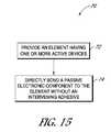
- FIG. 15is a flowchart illustrating a method for forming a bonded structure, according to various embodiments.
- FIG. 16is a schematic system diagram of an electronic system incorporating one or more bonded structures, according to various embodiments.
- the passive electronic componentcomprises a capacitor.
- the passive electronic componentcan comprise other devices, such as an inductor, a resistor, a voltage regulator, a filter, and/or a resonator.
- the passive electronic componentcan be integrated into a layer of passive components that is directly bonded to the semiconductor element (such as an integrated device die).
- the layer of passive componentscan be disposed between the semiconductor element and another system component such as an interposer, system substrate, etc.
- the passive electronic component described hereincan thereby reduce the space occupied by passive components at the integrated device, at the package, and/or at the system board. Moreover, positioning the passive electronic component closer to active components of the semiconductor element can beneficially reduce overall inductance, which can improve the bandwidth and signal integrity of the semiconductor element, as compared with passive devices that are mounted to the package substrate or system board. In addition, the overall capacitance provided by the disclosed embodiments enables significantly higher capacitances (and reduced inductance) as compared with discrete passives mounted to a die.
- the passive componentcan comprise a layered capacitor structure with a massive capacitance.
- high dielectric constant (high K) wafer or sheetscan be created with layered capacitors.
- a wafer-to-wafer bonding layercan be provided on a first element, such as a first semiconductor element or wafer (e.g., a processor wafer comprising a plurality of processors), and a second element, such as a second semiconductor element or wafer (e.g., a capacitor wafer that defines one or a plurality of capacitors).
- the first and second elements disclosed hereincan comprise semiconductor elements that are formed of a semiconductor material, or can comprise other non-semiconductor elements, such as various types of optical devices (e.g., lenses, filters, waveguides, etc.).
- an additional direct bonding layercan be added and prepared for direct bonding to both the capacitor wafer and the processor wafer.
- the layered capacitor structures disclosed hereinmay be used as alternating current (AC) coupling capacitors connected in series to a signal path to filter out direct current (DC) components of signals for balanced high-speed signaling.
- the layered capacitor structuremay also be used as a decoupling capacitor with high capacitance and extremely low parasitic inductance and resistance for reducing system power delivery network (PDN) impedance. Results show the capacitor structure enables operation for all frequency ranges with PDN impedance reduced by more than 1000 times compared with the use of discrete capacitors mounted to the die or package substrate.
- ACalternating current
- DCdirect current
- PDNsystem power delivery network
- the direct bond between the semiconductor element and the passive componentcan include a direct bond between corresponding conductive features of the semiconductor element (e.g., a processor die or wafer) and the passive component (e.g., a bond pad of the semiconductor element and a corresponding contact pad of the passive component) without an intervening adhesive, without being limited thereto.
- the conductive featuresmay be surrounded by non-conductive field regions.
- respective bonding surfaces of the conductive features and the non-conductive field regionscan be prepared for bonding. Preparation can include provision of a nonconductive layer, such as silicon oxide, with exposed conductive features, such as metal bond pads or contacts.
- the bonding surfaces of the conductive features and non-conductive field regionscan be polished to a very high degree of smoothness (e.g., less than 20 nm surface roughness, or more particularly, less than 5 nm surface roughness).
- the surfaces to be bondedmay be terminated with a suitable species and activated prior to bonding.
- the non-conductive surfaces (e.g., field regions) of the bonding layer to be bondedsuch as silicon oxide material, may be very slightly etched for activation and exposed to a nitrogen-containing solution and terminated with a nitrogen-containing species.
- the surfaces to be bondedmay be exposed to an ammonia dip after a very slight etch, and/or a nitrogen-containing plasma (with or without a separate etch).
- a direct bond interconnect (DBI) processnonconductive features of the die and the passive component layer can directly bond to one another, even at room temperature and without the application of external pressure, while the conductive features of the die and the passive component layer can also directly bond to one another, without any intervening adhesive layers. Bonding by DBI forms stronger bonds than Van der Waals bonding, including significant covalent bonding between the surfaces of interest.
- the respective conductive featurescan be flush with the exterior surfaces (e.g., the field regions) of the semiconductor element and the passive component. In other embodiments, the conductive features may extend above the exterior surfaces. In still other embodiments, the conductive features of one or both of the semiconductor element and the passive component layer are recessed relative to the exterior surfaces (e.g., nonconductive field regions) of the semiconductor element and the passive component. For example, the conductive features can be recessed relative to the field regions by less than 20 nm, e.g., less than 10 nm.
- the nonconductive field regions (such as silicon oxide) of the semiconductor elementcan be brought into contact with corresponding nonconductive regions of the passive component.
- the interaction of the activated surfacescan cause the nonconductive regions of the semiconductor element to directly bond with the corresponding nonconductive regions of the passive component without an intervening adhesive, without application of external pressure, without application of voltage, and at room temperature.
- the bonding forces of the nonconductive regionscan include covalent bonds that are greater than Van der Waals bonds and exert significant forces between the conductive features.
- the bonding energy of the dielectric-dielectric surfacecan be in a range from 150-300mJ/m 2 , which can increase to 1500-4000 mJ/m 2 after a period of heat treatment.
- direct bonding of the nonconductive regionscan facilitate direct metal-to-metal bonding between the conductive features.
- the semiconductor element and the passive componentmay be heated after bonding at least the nonconductive regions. As noted above, such heat treatment can strengthen the bonds between the nonconductive regions, between the conductive features, and/or between opposing conductive and non-conductive regions.
- there may be an initial gap between the conductive features of the semiconductor element and the passive component layerand heating after initially bonding the nonconductive regions can expand the conductive elements to close the gap. Regardless of whether there was an initial gap, heating can generate or increase pressure between the conductive elements of the opposing parts, aid bonding of the conductive features and form a direct electrical and mechanical connection.
- the capacitancecan be improved by providing capacitors that have electrode surfaces generally disposed along a direction non-parallel to (e.g., generally perpendicular to) a major lateral surface of the element (e.g., a semiconductor element).
- the undulations that provide the increased surfacescan be relatively simply patterned, compared to multiple layers and masks for producing laterally extending fins.
- the capacitorcan comprise first and second electrodes that include major surfaces extending along the non-parallel direction and spaced apart by an intervening dielectric.
- the vertically-disposed undulations (e.g., trenches) of the capacitorcan have a high aspect ratio, e.g., a first height of the first electrode along the non-parallel direction can be longer than a width of the capacitor along the major lateral surface.
- the aspect ratiowhich can be defined by the first height divided by the width, can be greater than 5:1.
- providing the capacitor primarily vertically relative to the semiconductor elementcan beneficially increase the overall surface area of the electrodes, improving capacitance relative to other arrangements.
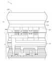
- FIG. 1Ais a schematic side view of a bonded structure 1 mounted to a carrier such as a package substrate 5 , according to various embodiments.
- the illustrated carriercomprises a package substrate, but in other embodiments, the carrier can comprise an integrated device die or any other suitable element.
- the package substrate 5can comprise any suitable substrate configured to mount to a system motherboard.
- the package substrate 5can comprise a printed circuit board (PCB), an interposer, a leadframe, a ceramic substrate, a polymer substrate, or any other suitable carrier.
- the package substrate 5can comprise a plurality of solder balls 6 to provide electrical connection with the system motherboard (not shown). In other embodiments, the package substrate 5 can electrically connect to the system motherboard in other ways.
- the bonded structure 1comprises an element (e.g., a semiconductor element 2 ) and a passive electronic component 3 directly electrically and mechanically connected with the element 2 .
- the element 2 illustrated in FIG. 1Acomprises a semiconductor element such as a processor die, but other types of integrated device dies or semiconductor elements can be used.
- the element 2can comprise a memory die, a microelectromechanical systems (MEMS) die, an optical device or die, an interposer, a reconstituted die or wafer, or any other suitable device or element.
- MEMSmicroelectromechanical systems
- the element 2 illustrated hereincan instead comprise a non-semiconductor element such that the passive electronic component 3 can be mechanically and electrically connected to other types of elements, such as optical elements (e.g., optical lenses, waveguides, filters, etc.), which may or may not comprise a semiconductor material.
- optical elementse.g., optical lenses, waveguides, filters, etc.
- the passive electronic component 3can be bonded to an active surface 11 of the semiconductor element 2 , i.e., active electronic circuitry can be defined at or near the active surface 11 of the semiconductor element 2 .
- the passive electronic component 3is directly bonded to the active surface 11 of the semiconductor element 2 without an intervening adhesive.
- the passive electronic component 3can be adhered to the semiconductor element 2 , e.g., by way of a microbump array with reflow, conductive pillars, or by a thermocompression bond.
- bonding the passive electronic component 3 to the front or active surface 11 of the semiconductor element 2can reduce the length of the signal lines and the overall impedance and/or inductance, as compared with systems which mount passive devices at the system board or package substrate.
- the passive component 3can reduce the voltage requirements for the semiconductor element 2 by acting to quiet the noisy components therein.
- bonding the passive electronic component 3 to the semiconductor element 2can reduce the overall dimensions of the package, since the passives occupy a thin layer bonded to the semiconductor element 2 .
- TSVsthrough silicon vias
- the passive electronic component 3can comprise a first surface 12 directly bonded to the semiconductor element 2 and a second exterior surface 13 opposite the first surface 12 of the passive electronic component 3 .
- a plurality of electrical contacts 4e.g., solder balls
- the plurality of electrical contacts 4can be configured to electrically connect to an external semiconductor element, such as the package substrate 5 shown in FIG. 1A (e.g., a printed circuit board, an interposer, etc.).
- the second surfaces 13can have exposed contacts or pads that are configured for direct bond connection to another element that serves as a carrier for the bonded structure, such as another semiconductor element (e.g., die or interposer).
- the passive electronic component 3can cover (e.g., can be disposed over) a majority of the active surface 11 of the semiconductor element 2 , e.g., a majority of the surface of the semiconductor element 2 that is used for processing or other active tasks.
- the passive electronic component 3can cover at least 55%, at least 65%, at least 75%, at least 85%, at least 95%, at least 99%, or at least 100% of the active surface 11 of the semiconductor element 2 .
- FIG. 1Athe passive electronic component 3 can cover (e.g., can be disposed over) a majority of the active surface 11 of the semiconductor element 2 , e.g., a majority of the surface of the semiconductor element 2 that is used for processing or other active tasks.
- the passive electronic component 3can cover at least 55%, at least 65%, at least 75%, at least 85%, at least 95%, at least 99%, or at least 100% of the active surface 11 of the semiconductor element 2 .
- a single unitary passive component 3is shown as covering substantially the entire active surface 11 of the semiconductor element 2 ; however, in other embodiments, the passive component 3 can comprise a plurality of discrete or separate passive components that are bonded to cover a majority of the active surface 11 of the element 2 .
- the passive electronic component 3may be mechanically and electrically connected to the back side of the semiconductor element 2 , i.e., the surface opposite the active surface 11 . In such arrangements, the length of conductors within the element 2 may be sufficiently short so as to sufficiently reduce impedance relative to routing to separate surface mounted passives on a packaging substrate, even though the passive component 3 is mounted to the back side of the element 2 .
- the passive electronic component 3can comprise a sheet that is bonded (e.g., directly bonded without an intervening adhesive) to the semiconductor element 2 , i.e., the passive electronic component 3 can be dimensioned so as to have a lateral width that is significantly larger than its thickness.
- the passive electronic component 3can have a lateral width (e.g., as defined along a direction parallel to the active surface 11 of the element 2 ) that is at least 3 times, at least 5 times, at least 10 times, or at least 50 times its thickness (e.g., as defined along a direction perpendicular to the active surface 11 of the element 2 ) of the component 3 .
- the passive electronic component 3can be provided on a sacrificial wafer (e.g., silicon or glass), and the semiconductor element 2 can also be provided on a wafer.
- the two waferscan be directly bonded to one another at the wafer level (e.g., wafer-to-wafer or W2 W), such that a plurality of passive components 3 can be bonded to a corresponding plurality of semiconductor elements 2 , which can improve manufacturing throughput.
- the base material of the waferscan be thinned or removed prior to or after dicing.
- the passive electronic component 3can be picked and placed on the semiconductor element 2 , or can be bonded to the semiconductor element 2 using other processing techniques.
- FIG. 1Bis a schematic side view of a semiconductor element 2 comprising a bulk material portion 37 (e.g., bulk semiconductor material) and active surface 11 , and a passive electronic component 3 prior to forming a bonded structure 1 .
- the features of FIG. 1Bmay be the same as or generally similar to like-numbered features of FIG. 1A .
- the passive component 3 and the semiconductor element 2can comprise respective bonding layers 8 a , 8 b (see also FIG. 2 ).
- the bonding layer 8 a of the passive electronic component 3can comprise one or a plurality of conductive features 9 a , 9 a ′, such as metal, surrounded by non-conductive field regions (see FIG.
- the bonding layer 8 bcan comprise one or a plurality of conductive features 9 b , 9 b ′, such as metal, surrounded by non-conductive field regions (see FIG. 2 ), such as silicon oxide.
- the conductive features 9 a , 9 a ′, 9 b , 9 b ′can act as electrical interconnects to provide electrical communication between the semiconductor element 2 and the passive component 3 .
- the conductive features 9 a , 9 a ′, 9 b , 9 b ′can comprise any suitable metal or conductor, such as copper.
- the conductive features 9 a , 9 a ′, 9 b , 9 b ′can be recessed below, can protrude above, or can be flush with, exterior surfaces of the non-conductive field regions.
- the conductive feature 9 acan comprise a first terminal (e.g., an anode of a capacitive device), and the other conductive feature 9 a ′ can comprise a second terminal (e.g., a cathode of a capacitive device) that is of a different type than the first terminal.
- the conductive feature 9 bcan comprise a first terminal of the element 2 (e.g., an anode), and the other conductive feature 9 a ′ can comprise a second terminal of the element 2 (e.g., a cathode) that is of a different type than the first terminal.
- various embodiments disclosed hereincan include both the anode and the cathode (e.g., conductive features 9 a , 9 a ′) on the same first surface 12 of the passive electronic component 3 .
- respective anode terminals 9 b of the semiconductor element 2can bond and electrically connect to corresponding respective anode terminals 9 a of the passive electronic component 3 disposed on the first surface 12 .
- Respective cathode terminals 9 b ′ of the semiconductor element 2can bond and electrically connect to corresponding respective cathode terminals 9 a ′ of the passive electronic component 3 disposed on the first surface 12 .
- each opposing side of the passive component 3can comprise one or a plurality of anodes and one or a plurality of cathodes (e.g., terminals of different types).
- one or both sides of the component 3can comprise one or more dummy terminals.
- An element(such as semiconductor element 2 ) can have contacts connected (e.g., bonded) to corresponding anode and cathode terminals on one side (e.g., a first side) of the passive component.
- a second element(such as another semiconductor element, a package substrate, etc.) can have contacts connected (e.g., bonded) to corresponding second anode and cathode terminal on the opposite side (e.g., a second side) of the passive component 3 .
- the element 2can connect to corresponding first and second terminals which are of a different type (e.g., anode and cathode terminals) on a first side of the passive component 3 .
- Another elementsuch as a package substrate can connect to corresponding first and second terminals which are of a different type (e.g., anode and cathode terminals) on the second opposite side of the passive component 3 , for example, by way of the interconnects 4 (which may comprise solder balls).
- a different typee.g., anode and cathode terminals
- the anode terminals 9 a , 9 bare directly bonded to one another without an intervening adhesive.
- the cathode terminals 9 a ′, 9 b ′can also be directly bonded to one another without an intervening adhesive.
- the respective anode terminals 9 a , 9 b and cathode terminals 9 a ′, 9 b ′can be connected by way of thermocompression bonding.
- the respective anode terminals 9 a , 9 b and cathode terminals 9 a ′, 9 b ′can be connected in other ways, e.g., by way of a conductive adhesive, such as solder, anisotropic conductive film, etc.
- a conductive adhesivesuch as solder, anisotropic conductive film, etc.
- various portions of the passive component 3can have different types of interconnects and/or passive components.
- one portion of the passive electronic component 3can comprise a multilayer capacitive portion, similar to the portion illustrated in FIG. 2
- another portion of the passive electronic component 3can comprise a series capacitive interconnect similar to what is shown in FIG. 4A .
- a low resistance electrical pathwaye.g., a through interconnect
- passive electronic componentssuch as those shown in FIGS. 7A-7C may also include anode and cathode terminals 9 a , 9 a ′ on the same side of the component.
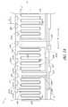
- FIG. 2is a schematic, magnified side cross-sectional view of portions of the semiconductor element 2 and the passive electronic component 3 shown in FIGS. 1A-1B , just prior to direct bonding.
- the passive component 3can comprise a bonding layer 8 a
- the semiconductor element 2can comprise a bonding layer 8 b .
- the bonding layer 8 acan comprise one or a plurality of conductive features 9 a , 9 a ′, such as metal, surrounded by non-conductive field regions 7 a , such as a form of silicon oxide material.
- the bonding layer 8 bcan comprise one or a plurality of conductive features 9 b , 9 b ′, such as metal, surrounded by non-conductive field regions 7 b , such as silicon oxide.
- the conductive features 9 a , 9 a ′, 9 b , 9 b ′can act as electrical interconnects to provide electrical communication between the semiconductor element 2 and the passive component 3 .
- the conductive features 9 a , 9 a ′, 9 b , 9 b ′can comprise any suitable metal or conductor, such as copper.
- the conductive features 9 a , 9 a ′, 9 b , 9 b ′can be recessed below, can protrude above, or can be flush with, exterior surfaces of the non-conductive field regions 7 a , 7 b .
- the non-conductive field regions 7 a , 7 bcan comprise any suitable non-conductive material, such as silicon oxide, undoped or very lightly doped silicon, silicon nitride, etc., that can be prepared for direct bonding.
- the bonding layers 8 a , 8 bcan be polished (e.g., by chemical mechanical polishing, or CMP) to a very low surface roughness (e.g., RMS roughness less than 20 nm, or more particularly, less than 5 nm).
- the bonding layers 8 a , 8 be.g., the non-conductive field regions 7 a , 7 b
- a suitable speciessuch as nitrogen, e.g., by way of exposure to a nitrogen-containing plasma (e.g., in a reactive ion etch) or by very slightly etching and subsequently exposing to a nitrogen-containing (e.g., ammonia) solution.
- the bonding layers 8 a , 8 bcan be brought together at room temperature in some embodiments to form a direct bond between the field regions 7 a , 7 b .
- the semiconductor element 2 and the passive component 3can be heated to strengthen the bond between the field regions 7 a , 7 b , and/or to cause the conductive features 9 a and 9 b , and 9 a ′ and 9 b ′ to expand and form an electrical connection.
- the use of a direct bondcan provide a low impedance and low inductance electrical pathway between the semiconductor element 2 and the passive component 3 , which can improve power or signal integrity.
- the semiconductor element 2can comprise internal conductive traces 14 and vias 15 to route electrical signals within the semiconductor element 2 and/or between the semiconductor element 2 and the passive electronic component 3 .
- the electrical signalscan pass through the conductive features 9 a , 9 a ′ and 9 b , 9 b ′ (which may be directly bonded to one another, respectively) to and/or from the passive electronic component 3 .
- the conductive features 9 a , 9 a ′can define, can act as, or can connect to a contact pad 21 at or near the first surface 12 of the passive electronic component 3 . As shown in FIG.
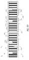
- the passive electronic component 3can comprise a plurality of (e.g., two or more, or three or more) conductive layers 16 spaced apart by one or a plurality of dielectric or nonconductive layers 10 .
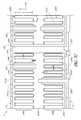
- the bonded structure 1can include conductive features 9 a , 9 a ′, 9 b , 9 b ′ that define an interconnect structure 17 that includes the contact pads 21 and electrical pathways or interconnects 18 between the semiconductor element 2 and the electrical contacts 4 on the second surface 13 of the passive electronic component 3 .
- each contact pad 21can comprise one conductive feature.
- FIG. 2illustrates three contact pads 21 and three interconnects 4
- the number of contact pads 21 and interconnects 4may differ.
- the pitch of the contact pads 21 on the semiconductor element 2 and/or passive component 3may be smaller than the pitch of the interconnects 4 .
- the pitch of the interconnects 4may be significantly greater than the pitch of the contact pads 21 , e.g., the pitch of the interconnects 4 may be at least 10 times, at least 20 times, at least 30 times the pitch of the contact pads 21 .
- the pitch of the interconnects 4can be in a range of 100 microns to 300 microns, or in a range of 100 microns to 200 microns (e.g., about 150 microns).
- the pitch of the contact pads 21can be in a range of 0.5 microns to 50 microns, in a range of 0.5 microns to 20 microns, or in a range of 1 micron to 10 microns (e.g. about 5 microns).
- a first conductive interconnect 18 aextends from the first surface 12 (or the contact pad 21 ) to a corresponding electrical contact 4 at the second surface 13 of the passive electronic component 3 .
- Second and third conductive interconnects 18 b , 18 ccan also extend from the contact pad 21 to corresponding electrical contacts 4 at the second surface 13 .
- each of the conductive electrical interconnects 18 a - 18 ccan comprise a longitudinal conductive portion 19 extending from a corresponding contact pad 21 at or near the first surface 12 to a corresponding electrical contact 4 . As shown in FIG.
- the longitudinal portions 19can extend vertically through the thickness of the passive electronic component 3 (e.g., transverse to the active surface 11 of the semiconductor element 2 ).
- the conductive interconnects 18 a - 18 ccan include one or more lateral conductive portions 20 extending laterally outward from the longitudinal conductive portions 19 .
- the longitudinal conductive portions 19can define resistive electrical pathways, and the one or more lateral conductive portions 20 can define capacitive electrical pathways in parallel with the resistive electrical pathways.
- the one or more lateral conductive portions 20 of the first interconnect 18 acan be interleaved with the lateral portions 20 of the second interconnect 18 b and can separated by the intervening dielectric layers 10 .
- the lateral conductive portions 20 of the second interconnect 18 bcan be interleaved with the lateral portions 20 of the third interconnect 18 c and can separated by the intervening dielectric layers 10 .
- the interleaving of the lateral portions 20 of the respective interconnects 18 a - 18 ccan define, at least in part, the respective capacitive electrical pathways, such that each lateral portion 20 acts as an electrode of a capacitor and the intervening dielectric layer 10 acts as the capacitor dielectric.
- the dielectric layer 10can comprise a high K dielectric layer, such as titanates, (BaxSr1-xTiO3, Bi4Ti3O12, PbZrxTi1-xO3), niobates (LiNbO3), and/or zirconates (BaZrO3, CaZrO3 etc).
- the dielectric layer 10may comprise any suitable dielectric material, such as silicon oxide, silicon nitride, etc.
- the dielectric layercan have a dielectric constant in a range of 1 to 1000.
- the dielectric layercan have a dielectric constant in a range of 1 to 10.
- the anode and cathode terminals of the passive component 3may be disposed along the same side of the component 3 .
- the first and third interconnect structures 18 a , 18 ccan be configured to connect to a power source, and the second interconnect structure 18 b can be configured to connect to electrical ground, or vice versa.
- the passive electronic component 3 of FIG. 2can beneficially act as multi-layer decoupling capacitors in parallel connection between power and ground to reduce power delivery network (PDN) impedance so as to improve power integrity.
- PDNpower delivery network
- providing the decoupling capacitorse.g., the capacitors defined by the interconnect structures 18 a - 18 c
- near the active surface 11 of the semiconductor element 2e.g., near switches of a processing die
- Decoupling capacitance(such as that provided by the disclosed embodiments) in the core region of the die can provide a stable power supply to the computation engines in electronic devices. Increasing this decoupling capacitance provides more stability in the voltage swings which reduces the amount of additional margins that are accommodated in timing analysis to account for voltage uncertainty. By contrast, adding decoupling capacitance in parallel plate structures offers relatively small capacitance values. Deep trench capacitors may provide higher capacitances but occupy a valuable footprint which may add area and cost to electronic devices.
- FIG. 3Ais a schematic side sectional view of a portion of a passive electronic component 3 configured for relatively low speed connections.
- FIG. 3Bis a schematic circuit diagram of the passive electronic component 3 of FIG. 3A .
- the passive component 3can comprise an electrical pathway 18 having a low resistance and low capacitance between the first and second surfaces 12 , 13 of the passive component 3 .
- the pathway 18can include a longitudinal conductive portion 19 that directly connects the contact pad 21 and the electrical contact 4 .
- the longitudinal conductive portion 19acts to short the signal between the contact pad 21 and the contact 4 .
- lateral conductive portions 20can be disposed offset from the longitudinal conductive portion 19 .
- the lateral conductive portions 20can be spaced from one another along the thickness of the passive component 3 and can be separated by intervening dielectric layer(s) 10 .
- the electrical pathway 18 defined in the passive component 3 of FIGS. 3A-3Bmay be suitable for relatively low speed connections, since the longitudinal conductive portion 19 shorts the connection between the contact pad 21 and the electrical contact 4 .
- FIG. 4Ais a schematic side sectional view of a portion of a passive electronic component 3 configured for high speed series link signaling.
- FIG. 4Bis a schematic circuit diagram of the passive electronic component 3 of FIG. 4A .
- the passive electronic component 3can act as a DC-blocking capacitor, which can serve various purposes.
- the passive electronic component 3can regulate the average DC-bias level (e.g., filtering out the DC component), can protect the transmitter/receiver from destructive overload events that can occur due to poor power-up sequencing, and/or can function as part of a circuit that detects when the lines are disconnected.
- the DC-blocking capacitordoes not distort the high frequency components of signals passing through it.
- the passive electronic component 3can comprise an electrical pathway that includes a multi-layer capacitor disposed between the contact pad 21 and the electrical contact 4 . Indeed, unlike the embodiment of FIG. 3A , in FIG.
- the pathway 18 between the contact pad 21 and the contact 4is a capacitive electrical pathway defined by a plurality of lateral conductive portions 20 spaced apart by intervening dielectric layer(s) 10 through the thickness of the passive electronic component 3 .
- the multiple layers shown in FIG. 4Acan function electrically as multiple capacitors electrically connected in series.
- the effective capacitance provided by the pathway 18 of FIG. 4Acan be in a range of 10 nF/mm 2 to 1 ⁇ F/mm 2 .
- the capacitor(s) defined along the electrical pathway 18can filter out DC components of signals to provide balanced, high-speed signaling (e.g., the pathway 18 can act as a high pass filter).
- positioning the passive component 3 closer to the active circuitry of the semiconductor element 2can further improve the performance of the bonded structure 1 and can reduce reflection noises.
- FIGS. 5A-5Iillustrate another embodiment in which a passive electronic component 3 is bonded (e.g., directly bonded) to a semiconductor element 2 .
- the anode and cathode terminals of the passive electronic component 3can be disposed along the same side or surface of the component 3 .
- the passive component 3can comprise a high dielectric constant (a high K) thin film capacitor layer with integrated interconnects for direct bonding and integration with other components, such as a processor.
- the passive component 3can comprise dielectric materials that have a dielectric constant greater than 5, greater than 10, greater than 20, or greater than 100.
- the semiconductor element 2can be manufactured in one facility (e.g., a complementary metal oxide semiconductor, or CMOS, facility), and the passive component 3 can be manufactured in another facility that can accommodate the processing parameters for the high K materials.
- the semiconductor element 2 and the passive component 3can be provided with bonding layers and can be directly bonded so as to connect the semiconductor element 2 and the passive component 3 .
- the embodiments disclosed hereincan enable the separate manufacture and subsequent integration of thin film, high K dielectric materials with any suitable type of semiconductor or optical element.
- FIG. 5Ais a schematic side sectional view of a passive electronic component 3 that incorporates a high K dielectric material to define a capacitive sheet.
- the passive electronic component 3can comprise a base 122 upon which the capacitive sheet can be defined.
- the base 122may be sacrificial, such that the base 122 can be removed prior to bonding the passive component 3 to the semiconductor element 2 .
- the base 122can comprise a semiconductor material, such as silicon.
- a first electrode 120can be formed on the base 122 in any suitable manner.
- the first electrode 120can be deposited on the base 122 using a metal organic chemical vapor deposition (MOCVD) process, a physical vapor deposition (PVD) or sputtering process, or a sol-gel process (spin on and cure).
- MOCVDmetal organic chemical vapor deposition
- PVDphysical vapor deposition
- sol-gel processsol-gel process (spin on and cure).
- the first electrode 120can comprise a refractory metal, such as platinum (Pt) or ruthenium (Ru).
- the first electrode 120can be deposited as a continuous or blanket film atop the base 122 , and can serve as a common electrode for multiple capacitors.
- a high K dielectric layer 110can be deposited or otherwise formed on the first electrode 120 .
- the dielectric layer 110can be deposited using CVD, PVD, powder sintering, or other suitable techniques.
- the dielectric layer 110can have a dielectric constant greater than 5, greater than 10, greater than 20, greater than 100, or greater than 200 (e.g., about 300), or greater than 1000.
- the dielectric layercan comprise a complex oxide high K material, such as the ternary oxide barium strontium titanate (BaSrTiO 3 or BST), other titanates, (BaxSr1-xTiO3, Bi4Ti3O12, PbZrxTi1-xO3), niobates (LiNbO3), and/or zirconates (BaZrO3, CaZrO3 etc).
- BSTternary oxide barium strontium titanate
- other titanatesBaxSr1-xTiO3, Bi4Ti3O12, PbZrxTi1-xO3
- niobatesLiNbO3
- zirconatesBaZrO3, CaZrO3 etc.
- a single thin dielectric layermay be used with the passive component 3 .
- multiple layers of dielectric materialmay be provided to form the dielectric layer 110 .
- a second electrode 121can be deposited on the dielectric layer 110 .
- the second electrode 121can be any suitable conductive material, such as a refractory metal, and particularly a noble metal (e.g., Pt or Ru).
- a noble metale.g., Pt or Ru
- the refractory or noble metals of one or both of the first electrode 120 and the second electrode 121can beneficially form a Schottky barrier (as opposed to ohmic contact) which can improve the performance of the capacitor. In the illustrated embodiment, therefore, the refractory or noble metals of the electrodes 120 , 121 can remain in the final bonded structure 1 to provide improved performance.
- the noble or refractory metal of the first and/or second electrodes 120 , 121can be plated with another metal (e.g., copper) to reduce resistance. In other embodiments, however, the first and/or second electrodes 120 , 121 may be removed after formation of the passive component 3 and replaced with another metal (e.g., copper) to serve as the first and second electrodes 120 , 121 .
- the second electrode 121can be patterned to define a number of gaps 123 between portions of the second electrode 121 . Patterning the electrode into a plurality of portions can define the overall capacitance provided by passive electronic component 3 . For example, larger portions of the second electrode 121 may provide increased area and increased capacitance, while smaller portions of the second electrode 121 may provide reduced area and reduced capacitance.
- the passive component 3can comprise an array of capacitive cells, with a cell being similar to that illustrated in FIG. 5A .
- the passive component 3can include cells having an effective capacitance per unit area of at least 5 nF/mm 2 , at least 10 nF/mm 2 , at least 20 nF/mm 2 , at least 50 nF/mm 2 , at least 100 nF/mm 2 , or at least 200 nF/mm 2 .
- the passive component 3can include cells having an effective capacitance per unit area in a range of 5 nF/mm 2 to 400 nF/mm 2 , in a range of 10 nF/mm 2 to 300 nF/mm 2 , in a range of 10 nF/mm 2 to 250 nF/mm 2 , in a range of 10 nF/mm 2 to 150 nF/mm 2 , or in a range of 10 nF/mm 2 to 100 nF/mm 2 .
- the passive component 3can include cells having an effective capacitance per unit area in a range of 1 nF/mm 2 to 10 nF/mm 2 , in a range of 10 nF/mm 2 to 100 nF/mm 2 , in a range of 100 nF/mm 2 to 400 nF/mm 2 , or above 400 nF/mm 2 (e.g., in a range of 400 nF/mm 2 to 1000 nF/mm 2 ).
- the high K dielectric materialmay be used, such that there are no low K materials in series with the high K material. By using only high K materials, the overall capacitance of the passive component 3 can be improved.
- FIG. 5Bis a schematic side sectional view of the passive electronic component 3 of FIG. 5A , with a bonding layer 8 a provided over the second patterned electrode 121 .
- the bonding layer 8 acan act as an interconnect layer, such as a redistribution layer (RDL) to bond the passive electronic component 3 to other structures, such as the element 2 .
- RDLredistribution layer
- the bonding layer 8 acan comprise conductive features 9 a connected to or defining contact pads and surrounding non-conductive field regions 7 a .
- the conductive features 9 acan comprise any suitable metal such as copper.
- the field regions 7 acan comprise any suitable non-conductive material, such as silicon oxide. As shown in FIG.
- the non-conductive field regions 7 acan be disposed in the gaps 123 of FIG. 5A so as to electrically separate the patterned portions of the second electrode 121 to define separate capacitive cells in some embodiments.
- providing the bonding layer 8 a (e.g., with metals such as copper) on the passive electronic component 3can enable the use of a low temperature anneal (e.g., less than 150° C.) to improve the direct bond and to reduce or eliminate thermal mismatch of materials due to different coefficients of thermal expansion (CTE).
- FIG. 5Cis a schematic side sectional view of a portion of the semiconductor element 2 prior to bonding.
- the semiconductor element 2can be the same as or generally similar to the semiconductor element 2 shown in FIG. 2 , with traces 14 and vias 15 providing electrical communication with the element 2 between the conductive features 9 b and active circuitry.
- FIG. 5Dis a schematic side sectional view of a bonded structure 1 , in which the semiconductor element 2 is directly bonded to the passive component 3 that includes a high K dielectric material.
- the bonding layers 8 a , 8 b of the passive component 3 and the semiconductor element 2can be polished to a very low surface roughness. The polished surfaces can be activated and terminated with a desired species (such as nitrogen).
- the bonding layers 8 a , 8 bcan be brought into direct contact (e.g., at room temperature) to form strong bonds between the respective field regions 7 a , 7 b , such as oxide materials.
- the structure 1can be heated to increase the bond strength and to cause electrical connection between the conductive features 9 a , 9 b .
- the passive electronic component 3can be directly bonded to the semiconductor element 2 along a direct bond interface 24 without an intervening adhesive.
- a direct bondcan provide a low impedance and low inductance electrical pathway between the semiconductor element 2 and the passive component 3 , which can improve power or signal integrity.
- the conductive features 9 a , 9 bcan be adhered to one another with a conductive adhesive (e.g., solder) or can be bonded using thermocompression bonding techniques.
- the base 122can be removed from the backside of the passive electronic component 3 (for example, by grinding, polishing, etching, etc.).
- the first electrode 120may also be patterned to further define the capacitance of the component 3 .
- noble or refractory metalscan be used during processing to define the passive electronic component 3 .
- the noble or refractory metals that serve as the first and second electrodes 120 , 121may not be removed and may thus remain in the resulting bonded structure 1 .
- the first electrode 120 and/or the second electrode 121can comprise sacrificial materials that can be removed and replaced by other metals.
- the passive electronic component 3is illustrated as being laterally wider than the semiconductor element 2 . However, it should be appreciated that the passive electronic component 3 may cover only a portion of the semiconductor element 2 . For example, as explained above, the passive component 3 can cover at least 55%, at least 65%, at least 75%, at least 85%, at least 95%, at least 99%, or at least 100% of the active surface 11 of the semiconductor element 2 .
- FIG. 5Fis a schematic side sectional view of a passive electronic component 3 with integrated power electrodes 126 (or signal electrodes) and ground electrodes 125 .
- FIG. 5Gis a top plan view of the passive electronic component 3 of FIG. 5F .
- the ground electrodes 125can extend from the first surface 12 , through the field regions 7 a and the dielectric layer 110 , and can contact the first electrode 120 .
- the first electrode 120can be connected to electrical ground, which can provide a ground pin or terminal when connected with the semiconductor element 2 .
- the power electrodes 126 shown in FIGS. 5A and 5Bcan comprise capacitive electrical pathways between the first surface 12 and the first electrode 120 .
- first electrode 120when connected to the semiconductor element 2 , electrical power can be transferred between the first surface 12 (by way of the conductive features 9 a and/or contact pads 21 ) and portions of the first electrode 120 , which can in turn connect to another structure, such as the package substrate 5 .
- the first electrode 120can be patterned or can be removed and replaced by an interconnect layer (such as a back-end of the line metallization layer) so as to provide electrical power along predefined electrical pathways.
- FIG. 5His a schematic side sectional view of a passive electronic component 3 according to another embodiment.
- FIG. 5Iis a top plan view of the passive electronic component 3 of FIG. 5H .
- the passive electronic component 3can include shorted power electrodes 127 , in addition to the power electrodes 126 and ground electrodes 125 shown in FIGS. 5F and 5G .
- some power electrodes 127may be connected to the second surface 13 of the component 3 by way of direct conductive interconnects.
- the power electrodes 126may comprise capacitive electrical pathways between the conductive features 9 a (or contact pads 21 ) and the second surface 13
- the shorted power electrodes 127may comprise conductive or resistive electrical pathways between the conductive features 9 a (or contact pads 21 ) and the second surface 13 .
- high K, thin film dielectric materialscan be used to define the passive electronic component 3 .
- the passive component 3may be manufactured in one facility in order to form the high K material and electrodes (which may comprise noble or refractory metals suitable for contact with high K materials), and the semiconductor element 2 can be formed in another facility to form the active components and interconnects of the element 2 .
- the noble or refractory metalscan be provided to enable high temperature processing.
- the noble or refractory metalscan be removed and replaced by other metals, such as copper, or by other metallization or routing layers.
- the noble or refractory metalscan be kept in the ultimate bonded structure 1 .
- the passive component 3can be bonded (e.g., directly bonded) to the semiconductor element 2 , which can provide a low impedance and low inductance connection to improve signal and/or power integrity of the bonded structure 1 .
- FIG. 6is a plot of the transfer impedance of various devices as a function of signal frequency, including a processor die without a capacitive element (plot A), a processor die with a 100 nF discrete capacitor mounted thereon (plot B), a processor die with a 100 nF capacitor mounted to the package substrate (plot C), a processor die with a 100 nF capacitive sheet similar to those disclosed in the embodiments of FIGS. 1-5I (plot D), a processor die with a 10 nF capacitive sheet similar to those disclosed in the embodiments of FIGS. 1-5I (plot E), and a processor die with a 1 nF capacitive sheet similar to those disclosed in the embodiments of FIGS. 1-5I (plot F).
- plot Aa processor die without a capacitive element
- plot Ba processor die with a 100 nF discrete capacitor mounted thereon
- plot Ca processor die with a 100 nF capacitor mounted to the package substrate
- the conventional devices reflected in plots A, B, and Chave relatively high transfer impedance values at frequencies above 500 MHz and/or above 1 GHz. Such high impedances above 500 MHz or 1 GHz may reduce the power or signal integrity of the processor dies.
- the embodiments disclosed hereinenable significantly reduced impedance at frequencies above 500 MHz, e.g., at or above 1 GHz, which can provide improved signal or power integrity at these higher frequencies.
- the embodiments disclosed hereincan provide impedance at 1 GHz that is at least 10 times, e.g., at least 100 times, less than the impedance of the conventional devices shown in Plots A-C.
- the directly bonded capacitance sheetsshow improved performance over discrete capacitors mounted on either the processor die or the package substrate.
- the embodiments disclosed hereincan provide the reduced impedance, even at significantly lower effective capacitances (e.g., at capacitances as low as about 1 nF or 10 nF).
- the embodiments disclosed hereincan advantageously provide reduced impedances with effective capacitance values in a range of about 0.5 nF to 10 mF, in a range of about 0.5 nF to 1 mF, in a range of about 0.5 nF to 1 ⁇ F, in a range of about 0.5 nF to 150 nF, in a range of about 1 nF to 100 nF, or in a range of about 1 nF to 10 nF.
- FIG. 7Ais a schematic side sectional view of a passive electronic component 3 , according to another embodiment.
- the passive electronic component 3 of FIG. 7Acan be bonded to the element 2 (which may comprise a semiconductor element or a non-semiconductor element) described herein.
- the passive electronic componentcan comprise a first surface 12 directly bonded to the element 2 (not shown in FIG. 7A ) without an intervening adhesive.
- a second surface 13can electrically connect to a package substrate (such as the substrate 5 ) or other packaging or system structure.
- capacitor 7Abeneficially comprises capacitors in which a majority of electrode surfaces are disposed non-parallel to (e.g., generally perpendicular to) the element 2 and the surfaces 12 , 13 .
- one or more capacitors 220can be defined in which a majority of electrode surfaces generally extend parallel to the z-axis, which can be non-parallel or perpendicular to the major surface of the passive element 3 (e.g., the x-y plane), e.g., the surfaces 12 , 13 .
- the capacitor 220can comprise a first electrode 221 a (which may comprise one of an anode and a cathode) and a second electrode 221 b (which may comprise the other of the anode and the cathode) spaced apart from one another by an intervening dielectric 210 .
- the anode and cathode terminals of the passive electronic component 3can be disposed along the same side or surface of the component 3 .
- the capacitor 220can be defined within a base 205 that can comprise an insulating or dielectric material, such as silicon, silicon oxide, etc.
- the electrodes 221 a , 221 b and the dielectric 210can include major surfaces that primarily extend along the direction non-parallel to the surfaces 12 , 13 , which corresponds to the z-axis in FIG. 7A .
- the capacitor 220can have a serpentine profile extending along the x-axis.
- the electrodes 221 a , 221 b and dielectric 210can have respective vertical portions 225 that are generally vertical, e.g., extending along the z-axis non-parallel or perpendicular to the first and second surfaces 12 , 13 .
- the vertical portions 225can be connected by corresponding lateral portions 226 of the electrodes 221 a , 22 b and dielectric 210 , such that the vertical portions 225 and the lateral portions 226 define a generally serpentine capacitor within the passive element 3 .
- a capacitance Ccan be provided between the two electrodes 221 a , 221 b along the entirety of the serpentine capacitor 220 .
- the overall capacitance C along the capacitor 220can be in a range of 100 nF/mm 2 to 20 ⁇ F/mm 2 , or in a range of 100 nF/mm 2 to 10 ⁇ F/mm 2 .
- the use of a serpentine capacitor in which the predominant surfaces of the capacitor 220 lie along planes parallel (or close to parallel) to the vertical z-axiscan significantly increase the overall surface area of the electrodes 221 a , 221 b , and, therefore, can accordingly increase the overall capacitance provided by the passive element 2 .
- the electrodes 221 a , 221 bcan comprise any suitable type of conductor, such as aluminum, silicon, doped silicon, nickel, or other materials.
- the dielectric 210can comprise any suitable dielectric material, such as aluminum oxide, silicon oxide, etc.
- increased capacitancecan be provided by using high dielectric materials (e.g., k>10), such as HfO 2 , ZrO 2 , BST, SBT, etc.
- the capacitors 220can electrically connect to the element 2 (not shown) by way of upper terminals 231 a , 231 b and to the package substrate 5 (not shown) or another element by way of lower terminals 232 a , 232 b .
- first terminals 231 acan provide electrical communication to the first electrode 221 a .
- Second terminals 231 bcan provide electrical communication to the second electrode 221 b which may be of a different type than the first terminals 231 a .
- first terminals 231 acan extend through the insulating base 205 to contact an upper portion of the first electrode 221 a , and can be exposed at the first surface 12 of the passive component 3 .
- the second terminals 231 bcan extend through the insulating base 205 and can contact an extension portion 236 of the second electrode 221 b .
- the extension portion 236 of the second electrode 221 bcan extend through the material of the first electrode 221 a , with the dielectric 210 intervening between the first electrode 221 a and the extension portion 236 of the second electrode 221 b .
- Still other ways to electrically connect to the capacitors 220may be suitable.
- first lower terminals 232 acan provide electrical communication to the first electrode 221 a .
- the second lower terminals 232 bcan provide electrical communication to the second electrode 221 b .
- upper terminals 231 acan electrically connect to the first electrodes 221 a (e.g., one of an anode or a cathode), and upper terminals 231 b can electrically connect to the second electrodes 221 b (e.g., the other of an anode and a cathode).
- each surface 12 , 13can comprise anode and cathode terminals (e.g., different types of terminals).
- the passive electronic component 3can also have a through signal connector 235 extending through the thickness of the passive electronic component 3 .
- the through signal connector 235can comprise a conductor that provides a conductive pathway between a first through signal terminal 234 on the first surface 12 and a second through signal terminal 233 on the second surface 13 .
- Any or all of the upper terminals 231 a , 231 b , the lower terminals 232 a , 232 b , and the through signal terminals 234 , 233can be configured for direct bonding to the element 2 and/or to the system board.
- the passive electronic component 3 shown in FIG. 7Acan beneficially provide capacitive pathway(s) and conductive through signal pathway(s).
- passive devices with relatively high capacitancecan be provided in line with the integrated circuit, without occupying separate real estate for the system, without interfering with direct signal connections.
- Disposing the capacitor 220 with a majority of electrode surfaces along (or close to parallel with) the vertical directioncan beneficially improve capacitance by significantly increasing the effective surface area of the electrodes 221 a , 221 b.
- the upper terminals 231 a , 231 b and the through signal terminals 234can be laterally spaced at a finer pitch than the lower terminals 232 a , 232 b and the through signal terminals 233 .
- an upper pitch p 1 of the terminals on the first surface 12e.g. the terminals 231 a , 231 b , and 234
- the upper pitch p 1can be in a range of 0.5 microns to 50 microns, in a range of 0.5 microns to 40 microns, in a range of 0.5 microns to 20 microns, in a range of 0.5 microns to 10 microns, or in a range of 1 micron to 10 microns.
- the fine pitch of the upper terminals 231 a , 231 b and the terminals 234can provide a relatively high number of channels for connection to the element 2 .
- a lower pitch p 2 of the lower terminals 232 a , 232 b and the terminals 233can be selected for suitable connection to the system motherboard.
- the lower pitch p 2can be less than 200 microns, or less than 150 microns.
- the lower pitch p 2can be in a range of 50 microns to 200 microns or in a range of 50 microns to 150 microns.
- the passive componentserves both to provide high capacitance passive devices and serves as an interposer without occupying separate real estate.
- the vertical capacitors 220can be defined in any suitable manner.
- the second electrode 221 bcan be defined from an initially planar sheet of porous silicon, porous aluminum, etc.
- the upper surface of the planar sheetcan be masked and etched such that channels can be etched into the sheet of the second electrode 221 b material.
- the dielectric 210can be conformally deposited into the channels over the etched surface of the porous aluminum or porous silicon.
- the dielectric 210can be deposited by physical vapor deposition (PVD), chemical vapor deposition (CVD) or atomic layer deposition (ALD).
- An additional conductive materiale.g., aluminum
- aluminumcan be deposited, coated or otherwise applied over the dielectric 210 to define the first electrodes 221 a .
- first and second electrodes 221 a , 221 bcan comprise the same material. In other embodiments, the first and second electrodes 221 a , 221 b can comprise different materials.
- the illustrated structure with vertical channels or finscan be readily defined with fewer masking steps compared to horizontal fins.
- FIG. 7Bis a schematic side sectional view of a passive electronic component 3 according to another embodiment.
- the passive electronic component 3 of FIG. 7Bcan comprise a capacitor 220 in which a majority of electrode surfaces are vertically positioned and that defines a serpentine pattern along the x-axis.
- Major surfaces of the first and second electrodes 221 a , 221 b and the intervening dielectric 210can primarily extend non-parallel or perpendicular to the first and second surfaces 12 , 13 .
- FIG. 7Bis a schematic side sectional view of a passive electronic component 3 according to another embodiment.
- reference numerals in FIG. 7Brefer to the same or similar features as like-numbered components in FIG. 7A .
- the passive electronic component 3 of FIG. 7Bcan comprise a capacitor 220 in which a majority of electrode surfaces are vertically positioned and that defines a serpentine pattern along the x-axis.
- first upper terminals 231 acan electrically connect to the first electrode 221 a at or near the first surface 12 .
- each surface 12 , 13 of the passive component 3can comprise anode and cathode terminals, such that anode and cathode terminals can be disposed along the same side or surface of the component 3 (e.g., terminals 231 , 231 b at surface 12 and terminals 232 a , 232 b at surface 13 ).
- a separate vertical connector 237can extend downwardly into the passive element 3 to electrically connect the second upper terminal 231 b with the second electrode 221 b.
- FIG. 7Cis a schematic side cross-sectional view of a passive electronic component 3 , in which one or more serpentine capacitors may be defined along both sides of the second electrode 221 b . Multiple, separate capacitors may be defined within the passive electronic component 3 in various embodiments.
- reference numerals in FIG. 7Crefer to the same or similar features as like-numbered components in FIGS. 7A and 7B .
- the passive electronic component 3 of FIG. 7Cwith a majority of electrode surfaces that can extend generally vertically and non-parallel relative to the first and second surfaces 12 , 13 . Further, as with FIGS. 7A-7B , in FIG.
- each surface 12 , 13 of the passive component 3can comprise anode and cathode terminals, such that anode and cathode terminals can be disposed along the same side or surface of the component 3 (e.g., terminals 231 , 231 b at surface 12 and terminals 232 a , 232 b at surface 13 ).
- upper capacitor(s) 220 acan be defined in an upper portion 240 a of the passive component 3
- lower capacitor(s) 220 bcan be defined in a lower portion 240 b of the passive component 3 .
- both sides of the initial planar sheet of aluminum or siliconcan be masked and simultaneously etched to define channels within the second electrode 221 b .
- Dielectric 210can be deposited on both the upper and lower portions 240 a , 240 b .
- conductive materialcan be deposited over the dielectric 210 on the upper and lower portions 240 a , 240 b to define the first electrode 221 a .
- the embodiment of FIG. 7Ccan beneficially further increase the overall surface area of the electrodes 221 a , 221 b and thus the overall capacitance of the passive electronic component 3 .
- FIG. 7Dis a schematic side cross-sectional view of a passive electronic component 3 , in which capacitor(s) 220 can be defined by aligned fibers (e.g., carbon fibers) extending along the non-parallel direction z.
- capacitor(s) 220can be defined by aligned fibers (e.g., carbon fibers) extending along the non-parallel direction z.
- reference numerals in FIG. 7Drefer to the same or similar features as like-numbered components in FIGS. 7A-7C .
- the passive electronic component 3 of FIG. 7Dcan have a majority of electrode surfaces that can extend generally vertically and non-parallel relative to the first and second surfaces 12 , 13 . Further, as with FIGS. 7A-7C , in FIG.
- each surface 12 , 13 of the passive component 3can comprise anode and cathode terminals, such that anode and cathode terminals can be disposed along the same side or surface of the component 3 (e.g., terminals 231 a , 231 b at surface 12 and terminals 232 a , 232 b at surface 13 ).
- fibers(such as elongate carbon fibers) can act as the second electrode 221 b .
- the fiberscan be coated with non-conductive material to define the dielectric 210 , and can be subsequently coated with conductive material to define the first electrode 221 a . Still other ways of forming the vertical capacitors 220 may be suitable.
- the capacitors 220 shown in FIGS. 7A-7Dcan be elongated, e.g., heights l of the electrode surfaces of the capacitors 220 (e.g., which may be defined by the lengths of the electrodes 221 a , 221 b ) along the non-parallel direction z may be longer than corresponding widths w of undulations of the capacitors 220 along the major lateral surface x-y.
- the widths wcan be defined according to the pitch of the capacitors 220 , e.g., a width of a single undulation of the capacitor.
- An aspect ratio of the capacitors 220can be defined by l divided by w.
- the aspect ratiocan be greater than 5:1.
- the elongate capacitors 220 illustrated in FIGS. 7A-7Dcan provide increased electrode surface area as compared with other passive devices without entailing greater masking steps.
- the increased surface areascan significantly increase overall capacitance, even when used with low dielectric constant materials.
- various types of elementssuch as dies or wafers
- very small or thin profile capacitorscan be embedded within an insulating material and can be included in a stacked die arrangement, to decouple adjacent bonded devices, for example.
- Dies or wafersmay be bonded in a stacked arrangement using various bonding techniques, including direct bonding, non-adhesive techniques such as the direct bonding techniques disclosed above (see for example, U.S. Pat. No. 7,485,968, which is incorporated by reference herein in its entirety).
- direct bondingit is desirable that the surfaces of the dies to be bonded be extremely flat and smooth. For instance, as explained above, the surfaces should have a very low variance in surface topology, so that the surfaces can be closely mated to form a lasting bond. It is also desirable that the surfaces be clean and free from impurities, particles, or other residue.
- capacitorse.g., multi-layered capacitors or other passive components
- an insulating materialsuch as a ceramic or polymer to form wafer level stackable capacitor or other passive devices.
- using a ceramic, polymer, or the likeresults in a device that may be planarized to have a smoother bonding surface than may be possible with some other conventional insulating materials.
- co-fired ceramic, liquid crystal polymer (LCP), glass, silicon, or other semiconductor, and like materialsmay be used in various embodiments.
- the ceramicis precast, or a paste or liquid may be used to form self-leveling bonding surfaces for the devices.
- the bonding surfaces of the capacitor devicescan be planarized after firing in preparation for bonding.
- the capacitors to be embeddedcan comprise single or multi-layered components (to provide the capacitance desired) with edge conductors to electrically couple the terminals of the capacitors.
- One or more of the capacitorscan be embedded in an insulating material (such as the “green sheet” illustrated in the figures) using a variety of techniques.
- the capacitorscan be deposited on a layer of insulating material (e.g., pre co-fired ceramic), and another layer of the insulating material can be placed or deposited over the capacitors.
- the two layers of insulating materialcan be pressed together, sandwiching the capacitors, and the combination can be fired.
- the insulating material layerscan be joined together during firing, forming a unified device, with the capacitors embedded within.
- the dielectric material of the capacitorcan be monolithically integrated with the layer(s) of insulating material.
- an additional layer of insulating materialcan be placed between the top and bottom insulating layers and around the capacitors (forming a middle layer that includes the capacitors). When the combination is fired, all of the insulating material layers can be joined together, forming a unified device.
- any number of insulating layersmay be used with any number of capacitors or layers of capacitors to form the device.
- the capacitorscan be coated with a liquid or paste insulating material that can be fired or cured to solidify the insulating material and form the embedded device.
- the insulating materialcan be selected to have a coefficient of thermal expansion (CTE) that is low, or that has a value close to the CTE value of the dies (which may be made of silicon in some examples) that will be bonded to the capacitive device.
- CTEcoefficient of thermal expansion
- the CTE of the capacitive devicecan be selected to be similar to the CTE of a logic device, processor, etc., to be bonded to the capacitive device, so that the combination of devices can be packaged together (in a stacked arrangement, for instance) if desired.
- Viasmay be formed in the capacitive device, through the insulating material, to allow signal or power transfer through the capacitive device or to the embedded capacitors.
- the viasmay be formed prior to or after firing the capacitive device.
- redistribution layersmay be formed on one or both surfaces of the capacitive device, which may be coupled to the vias if desired.
- conductive tracescan be coupled to the edge connectors of the capacitors to form external terminals for the capacitors on one or both surfaces of the capacitive device.
- the terminals for the capacitorscan be located one on each surface of the capacitive device (e.g., anode and cathode terminals can be on opposing sides of the capacitive device), both on a single surface of the capacitive device (e.g., anode and cathode terminals can be on the same side or surface of the capacitive device), or there may be terminals for each of the edge connectors on each side of the capacitive device (e.g., each surface of the capacitive device can comprise both anode and cathode terminals).
- two terminalsmay be connected to one edge connector of the capacitor and may be configured to carry a power signal from one side of the capacitive device to the other.
- Two other terminalsmay be connected to a second edge connector of the capacitor and may be configured to provide a ground from one side of the capacitive device to the other.
- one side of the capacitoris coupled to a power signal and the other side of the capacitor coupled to ground.
- the terminalsmay be coupled to one or more of the vias or to a redistribution layer (RDL) (on one or both surfaces) if desired.
- RDLredistribution layer
- the terminals, vias, and/or RDL connectionscan be formed as direct bonding interconnects on the one or more surfaces of the capacitive device, when the capacitive device is to be bonded using direct bonding techniques.
- at least some of the interconnectscan have a pitch in the range of a single micron, where the vias may have a size in the 10-15 micron range.
- the direct bonding interconnectsmay only be used on one surface of the capacitive device, with the terminals for the capacitors on the one surface.
- one or more cavitiesmay be formed into a surface of a pre-fired insulating material layer.
- a capacitorcan be deposited within each cavity and vias can be formed within the insulating layer (in any order).
- a redistribution layercan be formed over the layer and the capacitors, embedding the capacitors within the device.
- the opposite surfacecan be planarized, and another RDL formed on the planarized surface if desired.
- FIGS. 8A-8Cillustrate various techniques for embedding a capacitor 220 in an insulating layer, according to various embodiments.
- FIGS. 8D-8Eare schematic side sectional views of the passive electronic component 3 which can be formed using any of the techniques shown in FIGS. 8A-8C .
- FIG. 8Ais a schematic side sectional view of a first insulating layer 260 a , a plurality of capacitors 220 , and a second insulating layer 260 b , prior to forming the passive electronic component.
- the embodiments shown in FIGS. 8A-8Cillustrate a plurality of capacitors 220 , which may be used in wafer-level processing. In other embodiments, only one capacitor 220 may be provided.
- the capacitors 220can comprise any suitable type of capacitor, including, e.g., single-layered capacitors with a single dielectric layer between two conductive electrode layers, or multi-layered capacitors having a plurality of dielectric layers between a plurality of conductive electrode layers.
- the capacitors 220may also be similar to or the same as any of the capacitive structures disclosed herein, including horizontally- or vertically-oriented capacitors.
- the first and second insulating layers 260 a , 260 bcan comprise any suitable type of insulating or non-conductive material, such as a ceramic, a glass, or a polymer.
- the first and second insulating layers 260 a , 260 bcan comprise ceramics, such as aluminum oxide.
- the first and second insulating layers 260 a , 260 bcan comprise polymers, such as liquid crystal polymer (LCP).
- LCPliquid crystal polymer
- the first and second insulating layers 260 a , 260 bcan comprise soft or flexible ceramic green sheets, e.g., ceramic sheets that when heated or fired at or above a suitable firing temperature, harden to form a stiffer ceramic material.
- the capacitor 220can be provided on the first insulating layer 260 a .
- the second insulating layer 260 bcan be provided (e.g., deposited) on the capacitor 220 .
- the first and second layers 260 a , 260 bcan be pressed together such that the first and second layers 260 a , 260 b contact one another in gaps 262 and around edge portions 261 of the capacitors 220 .
- the first and second layers 260 a , 260 bcan accordingly conform around the capacitors 262 and can contact one another when pressed.
- the first and second layers 260 a , 260 b and the embedded capacitors 220can be fired or co-fired at a temperature at or above a ceramic firing temperature so as to cause the first and second layers 260 a , 260 b to meld or blend together to form a harder or stiffer structure.
- the first and second layers 260 a , 260 bcan comprise the same material in various embodiments. In other embodiments, the first and second layers 260 a , 260 b can comprise different materials. In arrangements in which the first and second layers 260 a , 260 b comprise different materials, the materials can be selected such that the materials harden at or around the same firing or co-firing temperature, e.g. the temperature or temperature range at which the first and second layers 260 a , 260 b are sufficiently hardened. For example, some materials may comprise high temperature ceramics (e.g. with a firing temperature at or above 1000° C.) or low temperature ceramics (e.g., those with a firing temperature at or above 500° C.
- high temperature ceramicse.g. with a firing temperature at or above 1000° C.
- low temperature ceramicse.g., those with a firing temperature at or above 500° C.
- the resulting passive electronic component 3is illustrated in FIG. 8D , which is described in more detail below.
- FIG. 8Bis a schematic side sectional view of a first insulating layer 260 a , a plurality of capacitors 220 , a second insulating layer 260 b , and an intermediate third insulating layer 260 c disposed between the first and second insulating layers 260 a , 260 b , prior to forming the passive electronic component.
- the embodiment of FIG. 8Bis generally similar to or the same as the embodiment of FIG. 8A .
- the method for forming a passive component of FIG. 8Bmay also form the passive component 3 shown in FIG. 8D .
- FIG. 8Athe method for forming a passive component of FIG. 8B may also form the passive component 3 shown in FIG. 8D .
- FIG. 8Athe passive component 3 shown in FIG. 8D .
- the intermediate third insulating layer 260 ccan be deposited around the side edges 261 of the capacitors 220 prior to firing.
- the third intermediate layer 260 ccan have a thickness selected such the first and second layers 260 a , 260 b can contact the intermediate layer 260 c with little or no applied pressure. In other arrangements, pressure may be applied to cause the first layer 260 a to contact the third layer 260 c and to cause the third layer 260 c to contact the second layer 260 b .
- the first layer 260 a , second layer 260 b , third layer 260 c , and the capacitors 220can be co-fired at a temperature sufficient to cause the layers 260 a - 260 c to meld or otherwise join together to form a unitary or unified device, e.g., the unified passive component 3 shown in FIG. 8D .
- FIG. 8Cis a schematic side sectional view of capacitors 220 embedded in an insulating layer 260 , prior to forming the passive electronic component.
- the embodiment of FIG. 8Cis generally similar to or the same as the embodiments of FIGS. 8A-8B .
- the method for forming a passive component of FIG. 8Bmay also form the passive component 3 shown in FIG. 8D .
- the first, second, and third insulating layers 260 a - 260 cmay be formed prior to depositing or connecting to the capacitors 220 .
- the embodiment of FIG. 8A-8Bin the embodiment of FIG.
- a powder or other solid mixturecan be provided on a carrier 263 .
- the capacitors 220can be provided over the power or mixture, and a solution can be added to the powder or mixture.
- the solutioncan cause the powder or mixture to thicken into a soft, flexible insulating layer 260 (e.g., a soft ceramic or polymer).
- the resulting soft, flexible layer 260can be molded or otherwise formed over and around the capacitors 220 to embed the capacitors 220 within the insulating layer 260 .
- the insulating layer 260 and the capacitors 260can be co-fired at a temperature sufficient to cause the layer 260 to meld, mix or otherwise join together to form a unitary or unified device, e.g., the unified passive component 3 shown in FIG. 8D .
- the carrier 263can be removed after co-firing.
- FIG. 8Ccan beneficially enable the formation of a passive component without utilizing multiple deposition processes, such as those shown in FIGS. 8A-8B . Rather, the base insulating layer 260 can be formed about the capacitors 220 and co-fired to form the passive component 3 in relatively few process steps.
- FIG. 8Dis a schematic cross-sectional view of a passive electronic component 3 formed using any of the techniques shown in FIGS. 8A-8C .
- the passive electronic component 3may include features similar to or the same as those shown in FIGS. 7A-7D , such that reference numerals in FIG. 8D may represent similar components to like reference numerals of FIGS. 7A-7D , except where noted.
- the capacitors 220can be embedded within a layer 250 of insulating material.
- the capacitors 220can be completely embedded in the layer 250 such that the layer 250 of insulating material is disposed along the side edges 261 of the capacitor 220 , as well as along upper and lower surfaces 264 a , 264 b of the capacitor 220 .
- the layer 250 of insulating materialcan comprise a first insulator 210 a formed by firing or co-firing the assemblies shown in FIGS. 8A-8C .
- the first insulator 210 acan comprise a hardened ceramic, polymer, glass, etc.
- the capacitors 220 shown in FIG. 8Dcan be defined at least in part by a first electrode 221 a , a second electrode 221 b , and a second insulator 210 b intervening between the first and second electrodes 221 a , 221 b .
- the first and second insulators 210 a , 210 bcan be selected so as to have similar co-firing temperatures, and/or with a relatively low CTE that matches the components to which the passive electronic component 3 is to be bonded (e.g., a semiconductor element 2 , which may comprise silicon).
- the insulators 210 a , 210 bcomprise the same material.
- the insulators 210 a , 210 bcomprise different materials that each have firing temperatures at which the layers 210 a , 210 b both harden and merge or meld with one another.
- the first and second insulators 210 a , 210 bcan merge or mix with one another to form a monolithically integrated and unified or unitary structure.
- the monolithically integrated insulator 210 a of the layer 250may seamlessly integrate with the insulator 210 b of the capacitor 220 .
- the insulators 210 a , 210 bcan comprise dielectrics in various embodiments, e.g., ceramic dielectrics. In other embodiments, the insulators 210 a and/or 210 b may comprise polymers, glass, etc.
- the capacitor 220can comprise first terminal(s) 232 a connected to the corresponding first electrode(s) 221 a .
- Second terminal(s) 232 bcan be connected to corresponding second electrode(s) 221 b of the capacitor 220 .
- Each of the first and second terminals 232 a , 232 bcan be defined at least in part by respective outermost layers of the electrodes 221 a , 221 b (e.g., those electrodes 221 a , 221 b disposed at or near the respective upper and lower surfaces 264 a , 264 b of the capacitor 220 ), and by edge connectors 251 a , 251 b that electrically connect respective alternating electrodes 221 a , 221 b .
- the first edge connector 251 acan be disposed vertically, e.g., non-parallel relative to the electrodes 221 a and can electrically connect respective ends of the electrodes 221 a .
- the second edge connector 251 bcan be disposed vertically, e.g., non-parallel relative to the electrodes 221 b and can electrically connect respective ends of the electrodes 221 b .
- the electrodes 221 a , 221 bmay be of a different type, e.g., one electrode 221 a may comprise an anode and the other electrode 221 b may comprise a cathode, or vice versa.
- one or more through signal connectors 235can extend through the thickness of the passive electronic component 3 , from a first surface 265 a of the insulating layer 250 to a second surface 265 b of the insulating layer 250 .
- the through signal connectors 235can be formed after co-firing and forming the passive component 3 .
- the insulating layers 260 a , 260 b , and/or 260 c , and the capacitors 220can be co-fired to form a passive component.
- the through signal connectors 235can be provided or deposited in the holes.
- the conductive material for the connectors 235may not be able to withstand the high temperatures used during the firing or co-firing process.
- the connectors 235can comprise a conductor with material properties configured to withstand the high temperatures used for firing the structure. In such arrangements, the connectors 235 may be co-fired along with the capacitors 220 and insulating layers 260 a - 260 c.
- FIG. 8Eis a schematic side sectional view of the passive electronic component 3 shown in FIG. 8D , with one or more redistribution layers (RDLs) 252 a , 252 b (e.g., interconnect layer(s)) applied to the passive electronic component 3 .
- the RDLs 252 a , 252 bcan be provided on at least one of the first surface 265 a and the second surface 265 b of the insulating layer 250 .
- the RDLs 252 a , 252 bcan be pre-formed in some embodiments, prior to providing on the component 3 .
- the RDLs 252 a , 252 bcan be pre-formed and directly bonded to the component 3 without an intervening adhesive.
- the RDLs 252 a , 252 bcan be built up in layers over the insulating layer 250 .
- the RDLs 252 a , 252 bcan be configured to route electrical signals between selected terminals of the capacitors 220 and corresponding terminals or contact pads of the element(s) to which the passive electronic component 3 is to be connected.
- a first RDL 252 acan be provided over the first surface 265 a of the insulating layer 250 .
- a second RDL 252 bcan be provided over the second surface 265 b of the insulating layer 250 .
- the RDLs 252 a , 252 bcan comprise a plurality of metallic traces at least partially embedded in corresponding RDL insulating layers 266 a , 266 b .
- the first surface 12 of the passive component 3can be defined at an upper surface of the RDL 252 a
- the second surface 13 of the passive component 3can be defined at a lower surface of the RDL 252 b.
- first conductive traces 253 a or conductive vias of the respective RDLs 252 a , 252 bcan electrically connect to the first electrodes or terminals 221 a of the capacitor at or by way of the first terminals 232 a .
- the traces 253 a or vias(also referred to as interconnect(s)) can extend through at least a portion of the insulating material, or insulator 210 b to connect to respective terminals of the capacitor.
- second conductive traces 253 b of the respective RDLs 252 a , 252 bcan electrically connect to the second electrodes 221 b at or by way of the second terminals 232 b .
- the terminals 232 a , 232 bcan be defined at least in part by respective portions of the edge connectors 251 a , 252 b (which connect interleaving electrodes 221 a , 221 b .), and by outermost electrodes 221 a , 221 b (e.g., the electrodes 221 a , 221 b at or near the respective first or second surfaces 265 a , 265 b of the capacitors 220 ).
- electrical connection to the respective electrodes 221 a , 222 bcan be made to the edge connectors 251 a , 251 b and/or to the outermost electrodes 221 a , 221 b at the surfaces 265 a , 265 b.
- the traces 253 a , 253 bcan electrically connect the terminals 232 a , 232 b to respective interconnects 254 a , 254 b at the first or second surfaces 265 a , 265 b of the insulating material layer 250 .
- the interconnects 254 a , 254 bcan extend through the RDL insulators 266 a , 266 b and can be exposed at the first and second surfaces 12 , 13 .
- the insulating layers 266 a , 266 bcan act as respective layers or substrates through which the interconnects (or portions thereof) can extend to connect to the capacitor.
- the exposed surfaces of the interconnects 254 a , 254 bcan be configured to electrically connect to other elements, such as elements 2 (e.g., semiconductor elements such as integrated device dies), package substrates, interposers, etc.
- elements 2e.g., semiconductor elements such as integrated device dies
- the RDL insulating layers 266 a , 266 b and the exposed surfaces of the interconnects 254 a , 254 b at the surfaces 12 , 13can be polished and prepared for direct bonding in various embodiments.
- the insulating layers 266 a , 266 b and the exposed interconnects 254 a , 254 bcan be directly bonded to corresponding insulating and/or conductive features of other elements, without an intervening adhesive.
- elementsmay be bonded to both surfaces 12 , 13 of the component 3 . In other embodiments, elements may be bonded to only one surface 12 or 13 of the passive component 3 . In still other embodiments, the insulating layers 266 a , 266 b and/or the interconnects 254 a , 254 b can be bonded to the other elements with various adhesives.
- each surface 12 , 13 of the passive component 3can comprise first and second respective interconnects 254 a , 254 b that connect to different types of terminals 232 a , 232 b on each side of the capacitor 220 .
- each of the surfaces 265 a , 265 b of the insulating material 250can comprise an anode and a cathode terminal.
- one surface 265 acan comprise anode terminal(s) and the other surface 265 b can comprise cathode terminal(s).
- terminals 232 amay connect to electrical power, and other terminals 232 b may connect to electrical ground, or vice versa.
- FIGS. 9A-9Eillustrate a process for forming a passive electronic component 3 according to various embodiments.
- the components of FIGS. 9A-9Ecan be similar to or the same as like numbered components of FIGS. 7A-8E .
- FIG. 9Ais a schematic side sectional view of an insulating layer 250 .
- the insulating layer 250can comprise any suitable type of insulator, such as a ceramic, a polymer, a glass, a semiconductor (e.g., silicon), etc.
- one or more cavities 267can be formed in the insulating layer 250 , e.g., by etching, drilling, etc.
- the through signal interconnects 235can also be provided through at least a portion of the thickness of the insulating layer 250 .
- holescan be formed (e.g., drilled, etched, etc.), and conducive material can be provided in the holes to form the vias or interconnects 235 .
- one or more capacitors 220can be provided in the cavities 267 .
- a low CTE insulating filler 268can be provided over and/or around the capacitors 220 in the cavities 267 in order to support, stabilize, and/or reduce stress on the capacitors 220 .
- the first RDL 252 acan be provided over the first surface 265 a of the insulating layer 250 .
- Interconnects 254 a in the first RDL 252 acan connect to corresponding terminals 232 a of the capacitor 220
- other interconnects 254 b (not shown) in the first RDL 252 acan connect to corresponding terminals 232 b of the capacitor 220 .
- portions of the interconnects 254 a , 254 bcan extend through the insulating layer 266 a , 266 b of the RDLs 252 a , 252 b (which can act as insulating layers or substrates) to connect to the capacitor.
- FIG. 9Dthe first RDL 252 a can be provided over the first surface 265 a of the insulating layer 250 .
- Interconnects 254 a in the first RDL 252 acan connect to corresponding terminals 232 a of the capacitor 220
- the back side of the insulating material 250can be partially removed (e.g., polished, grinded, etched, etc.) to expose the surface 264 b of the capacitor 220 and the ends of the vias 235 .
- the second RLD 252 bcan be provided over the surface 265 b of the insulating material 250 and the surface 264 b of the capacitor 220 .
- the RDLs 252 a , 252 bcan be bonded (e.g., direct bonded in some arrangements) to the insulating layer 250 and the capacitors 220 .
- the RDLs 252 a , 252 bcan be bonded in other ways, e.g., using adhesives.
- the RDLs 252 a , 252 bcan be built up layer-by-layer.
- the capacitor 3can be embedded in the insulating layer 250 , which can act as an insulating element between the insulating layers 266 a , 266 b .
- the insulating layer 250can be disposed along the side edges 261 of the capacitors 220 , and may cover a majority of the side edges 261 , e.g., all or substantially the entirety of the side edges 261 .
- the RDLs 252 a , 252 bcan be provided over the upper and lower surfaces 264 a , 264 b of the capacitors 220 . Unlike FIGS.
- each surface 12 , 13 of the passive component 3can comprise different types of terminals, e.g., each surface 12 , 13 can comprise an anode terminal or interconnect and a cathode terminal or interconnect. In other embodiments, one surface 12 may comprise only anode terminals or interconnects, and the other surface 13 may comprise only cathode terminals or interconnects, or vice versa.
- a pitch of the interconnects 254 a and/or 254 b on the first surface 12 of the componentmay have a pitch smaller than a pitch of the interconnects 254 a , 254 b on the second surface 13 .
- the interconnects 254 a and/or 254 b on the first surface 12may be spaced and configured for direct bonding to another element.
- a pitch of the interconnects 254 a and/or 254 b on the first surface 12can be 50 microns or less, 10 microns or less, or 1 micron or less.
- terminals of the capacitor 220can be connected to corresponding interconnects 254 a and/or 254 b of the RDL at the first surface 12 , and may not be connected to any interconnects at the second surface 13 , or vice versa.
- FIGS. 10A-10Gillustrate another method for forming a passive electronic component 3 in which the passive component is embedded in an insulating layer 250 .
- FIG. 10Ais a schematic side sectional view of a first insulating substrate 270 a .
- the first insulating substrate 270 acan comprise any suitable type of insulator, such as a ceramic, a polymer, a glass, an insulating composite, etc.
- the substrates 270 a , 270 bcan comprise a material that has a coefficient of thermal expansion (CTE) of no more than 6 ppm/° C., or no more than 5 ppm/° C.
- CTEcoefficient of thermal expansion
- the CTE of the substrates 270 a , 270 bcan be in a range of 2 ppm/° C. to 6 ppm/° C., in a range of 3 ppm/° C. to 6 ppm/° C., or in a range of 3 ppm/° C. to 5 ppm/° C.
- the substrates 270 a , 270 bcan comprise the same material. In other embodiments, the substrates 270 a , 270 b may comprise different materials.
- a first adhesive 250 acan be applied or deposited on the first insulating substrate 270 a .
- the first adhesive 250 acan comprise any suitable type of adhesive, such as an insulating adhesive.
- the first adhesive 250 acan comprise a non-conductive epoxy.
- the capacitors 220can be provided (e.g., placed, deposited, etc.) on the first adhesive layer 250 a .
- the capacitors 220can partially embed within the first adhesive layer 250 a such that at least a portion of the first adhesive layer 250 a is disposed along the side edge 261 of the capacitor 220 and that at least another portion of the first adhesive layer 250 a is disposed along the second surface 264 b of the capacitor 220 .
- a second adhesive layer 250 bcan be provided or applied over and around the capacitors 220 . As shown in FIG.
- the second adhesive layer 250 bcan be disposed along the side edge 261 of the capacitor 220 , and at least another portion of the second adhesive layer 250 b can be disposed along the first surface 264 a of the capacitor 220 .
- a second insulating substrate 270 b(which may comprise the same insulating material or a different insulating material from the first substrate 270 a ).
- the insulating layer 250can comprise the first and second adhesive layers 250 a , 250 b , and the capacitors 220 can be fully embedded within the insulating layer.
- conductive interconnectscan be formed in the passive component 3 .
- the through conductive vias 235can be provided in through holes provided through the thickness of the passive component 3 , so as to provide through electrical communication in the component 3 .
- interconnects 254 a , 254 bcan be formed in corresponding holes of the insulating substrates 270 a , 270 b in order to electrically connect with corresponding terminals 232 a , 232 b of the capacitors 220 .
- the insulating substrates 270 a , 270 bcan act as interconnect layers to provide electrical communication with other elements or devices.
- each surface 12 , 13 of the passive component 3can comprise different types of terminals, e.g., each surface 12 , 13 can comprise an anode terminal or interconnect 254 a and a cathode terminal or interconnect 254 b .
- one surface 12may comprise only anode terminals or interconnects, and the other surface 13 may comprise only cathode terminals or interconnects, or vice versa.
- the adhesives 250 a , 250 bcan serve as an insulating element disposed between the first and second substrates.
- the interconnects 254 a , 254 bcan act as conductive vias that extend through at least a portion of the insulating element (e.g., portions of the first and second adhesives 250 a , 250 b ). Further, the interconnects 254 a , 254 b can extend through the substrates 270 a , 270 b to connect to the capacitors.
- the adhesives 250 a , 250 bcan be disposed adjacent to (and/or contacting) side edges of the capacitor 220 .
- the capacitors 220can be disposed in a first region between the first and second substrates 270 a , 270 b , and the insulating element (e.g., adhesives 250 a , 250 b of the insulating material 250 ) can be disposed in a different second region between the first and second substrates 270 a , 270 b .
- the use of the low CTE substrates 270 a , 270 b and intervening insulating material 250can provide the overall passive component 3 with a low overall effective CTE that is close to the CTE of the component(s) to which the passive component 3 is to be mounted, e.g. a semiconductor or silicon substrate.
- the overall effective CTE of the passive component 3can be no more than 8 ppm/° C., no more than 7 ppm/° C., or no more than 6 ppm/° C.
- the overall effective CTE of the passive component 3(also referred to as a microelectronic device herein) can be in a range of 3 ppm/° C. to 7 ppm/° C., in a range of 4 ppm/° C. to 8 ppm/° C., or in a range of 4 ppm/° C. to 7 ppm/° C.
- FIG. 10Fillustrates an alternative method for forming a passive component after the step shown in FIG. 10C .
- a molding compound 269can be provided at least around the side edges 261 of the capacitors 220 .
- the molding compound 269can comprise an insulating sub-layer of the insulating layer 250 , e.g., the molding compound 269 can comprise a non-conductive epoxy, encapsulant, etc.
- the molding compound 269may be applied around only the side edges 261 .
- the molding compound 269can be applied around the side edges 261 and the surfaces 264 a of the capacitors. The portions of the molding compound 269 over the surfaces 264 a may be removed in any suitable manner.
- the second adhesive layer 250 b(which can comprise a non-conductive or insulating adhesive) can be applied over the first surface 264 a and the upper surface of the molding compound 269 .
- the second insulating substrate 270 bcan be provided over the second adhesive layer 250 b .
- the insulating layer 250can comprise the first and second adhesive layers 250 a , 250 b and the molding compound 269 .
- the capacitors 220can be embedded in (e.g., completely embedded in) the insulating layer 250 .
- through vias 235 and interconnects 254 a , 254 bcan be provided to provide electrical communication through the component 3 and to the capacitors 220 , respectively.
- the adhesives 250 a , 250 b , and the molding compound 269can serve as an insulating element disposed between the first and second substrates 270 a , 270 b .
- the interconnects 254 a , 254 bcan act as conductive vias that extend through at least a portion of the insulating element (e.g., portions of the first and second adhesives 250 a , 250 b ). Further, the interconnects 254 a , 254 b can extend through the substrates 270 a , 270 b to connect to the capacitors.
- the adhesives 250 a , 250 bcan be disposed adjacent to (and/or contacting) upper surfaces of the capacitor 220 .
- the molding compound 269can be disposed adjacent to (and or contacting) side edges of the capacitors 220 .
- the capacitors 220can therefore be embedded within the insulating element (e.g., embedded within the adhesives 250 a , 250 b and the molding compound 269 .
- the capacitors 220can be disposed in a first region between the first and second substrates 270 a , 270 b , and at least a portion of the insulating element (e.g., adhesives 250 a , 250 b of the insulating material 250 ) can be disposed in a different second region between the first and second substrates 270 a , 270 b .
- the use of the low CTE substrates 270 a , 270 b and intervening insulating material 250can provide the overall passive component 3 with a low overall effective CTE that is close to the CTE of the component(s) to which the passive component 3 is to be mounted, e.g. a semiconductor or silicon substrate.
- the overall effective CTE of the passive component 3e.g., including the insulating and conductive materials shown in FIG. 10G
- the overall effective CTE of the passive component 3can be no more than 8 ppm/° C., no more than 7 ppm/° C., or no more than 6 ppm/° C.
- the overall effective CTE of the passive component 3(also referred to as a microelectronic device herein) can be in a range of 3 ppm/° C. to 7 ppm/° C., in a range of 4 ppm/° C. to 8 ppm/° C., or in a range of 4 ppm/° C. to 7 ppm/° C.
- the component 3 of FIGS. 10A-10Gcan comprise a laminated structure in which a plurality of substrates (such as substrates 270 a , 270 b ) can be coupled to one or more capacitors, e.g., by way of one or more adhesives and/or by way of a molding compound.
- the substrates 270 a , 270 bmay comprise materials or layers that are laminated or applied to the capacitor 220 without being deposited using a deposition process.
- FIGS. 11A-11Gillustrate another method for forming a passive electronic component 3 in which the passive component is embedded in an insulating layer 250 .
- FIGS. 11A-11Bare generally the same as FIGS. 10A-10B , respectively.
- a third insulating substrate 270 ccan be provided over the first adhesive layer 250 a and around the capacitors 220 .
- the third insulating substrate 270 cmay be the same material as the substrates 270 a , 270 b . In other embodiments, the material of the third substrate 270 c may differ from the material(s) of the substrates 270 a , 270 b .
- the first adhesive layer 250 acan be provided over the second surface 264 b and over portions of the side edges 261 . As shown in FIG. 11C , beneficially, first via portions 235 a can be provided through the third insulating substrate 270 . The first via portions 235 a can define a part of the through signal via or interconnect 235 .
- the second adhesive 250 bcan be provided over and around the capacitors 220 .
- the second adhesive layer 250 bcan be provided around portions of the side edges 261 of the capacitors 220 and over the first surfaces 264 a of the capacitors 220 .
- the second insulating substrate 270 bcan be provided or deposited over the second adhesive layer 250 b .
- the capacitors 220can be embedded in the insulating layer 250 , which can comprise the first and second adhesive layers 250 a , 250 b .
- the capacitors 220can be completely or fully embedded in the insulating layer 250 , such that portions of the insulating layer cover most or all of the surfaces of the capacitors 220 .
- interconnects 254 a , 254 bcan be provided to connect to the terminals 232 a , 232 b of the capacitors 220 .
- Second via portions 235 bcan be provided in each of the first and second insulating substrates 270 a , 270 b .
- the second via portions 235 bcan be electrically connected to the first via portions 235 a formed through the third insulating substrate 270 c .
- the first via portions 235 acan be directly bonded to corresponding second via portions 235 b without an intervening adhesive.
- the first vias portions 235 acan be bonded to second via portions 235 b with a conductive adhesive.
- the third insulating substrate 270 ccan enable a layer-by-layer construction of the resulting through via or interconnect 235 , without providing through holes through the insulating layer 250 .
- the third insulating substrate 270 ccan have a thickness about the same as the thickness of the capacitors 220 such that separate vias need not be formed through the insulating layer 250 .
- the adhesives 250 a , 250 b , and the third substrate 270 ccan serve as an insulating element disposed between the first and second substrates 270 a , 270 b .
- the interconnects 254 a , 254 bcan act as conductive vias that extend through at least a portion of the insulating element (e.g., portions of the first and second adhesives 250 a , 250 b ). Further, the interconnects 254 a , 254 b can extend through the substrates 270 a , 270 b to connect to the capacitors.
- the insulating material 250can be disposed adjacent to (and/or contacting) upper surfaces of the capacitor 220 and side edges of the capacitors 220 .
- the capacitors 220can therefore be embedded within the insulating element.
- the capacitors 220can be disposed in a first region between the first and second substrates 270 a , 270 b , and at least a portion of the insulating element (e.g., portions of adhesives 250 a , 250 b and the third substrate(s) 270 c ) can be disposed in a different second region between the first and second substrates 270 a , 270 b .
- the use of the low CTE substrates 270 a , 270 b , the third intervening substrate 270 c , and intervening insulating material 250can provide the overall passive component 3 with a low overall effective CTE that is close to the CTE of the component(s) to which the passive component 3 is to be mounted, e.g. a semiconductor or silicon substrate.
- the overall effective CTE of the passive component 3e.g., including the insulating and conductive materials shown in FIG. 11E
- the overall effective CTE of the passive component 3(also referred to as a microelectronic device herein) can be in a range of 3 ppm/° C. to 7 ppm/° C., in a range of 4 ppm/° C. to 8 ppm/° C., or in a range of 4 ppm/° C. to 7 ppm/° C.
- FIG. 11Fillustrates an alternative method for forming a passive component after the step shown in FIG. 11C .
- a molding compound 269can be provided at least around the side edges 261 of the capacitors 220 .
- the molding compound 269can comprise an insulating sub-layer of the insulating layer 250 , e.g., the molding compound 269 can comprise a non-conductive epoxy, encapsulant, etc.
- the molding compound 269may be applied around only the side edges 261 . In other embodiments, the molding compound 269 can be applied around the side edges 261 and the surfaces 264 a of the capacitors. The portions of the molding compound 269 over the surfaces 264 a may be removed in any suitable manner.
- the second adhesive layer 250 b(which can comprise a non-conductive or insulating adhesive) can be applied over the first surface 264 a and the upper surface of the molding compound 269 .
- the second insulating substrate 270 bcan be provided over the second adhesive layer 250 b .
- the insulating layer 250can comprise the first and second adhesive layers 250 a , 250 b and the molding compound 269 .
- the capacitors 220can be embedded in (e.g., completely embedded in) the insulating layer 250 .
- through vias 235 and interconnects 254 a , 254 bcan be provided to provide electrical communication through the component 3 and to the capacitors 220 , respectively.
- the adhesives 250 a , 250 b , and the molding compound 269can serve as an insulating element disposed between the first and second substrates 270 a , 270 b .
- the interconnects 254 a , 254 bcan act as conductive vias that extend through at least a portion of the insulating element (e.g., portions of the first and second adhesives 250 a , 250 b ). Further, the interconnects 254 a , 254 b can extend through the substrates 270 a , 270 b to connect to the capacitors.
- the adhesives 250 a , 250 bcan be disposed adjacent to (and/or contacting) upper surfaces of the capacitor 220 .
- the molding compound 269can be disposed adjacent to (and or contacting) side edges of the capacitors 220 .
- the capacitors 220can therefore be embedded within the insulating element (e.g., embedded within the adhesives 250 a , 250 b and the molding compound 269 ).
- the capacitors 220can be disposed in a first region between the first and second substrates 270 a , 270 b , and at least a portion of the insulating element (e.g., adhesives 250 a , 250 b of the insulating material 250 and the molding compound 269 ) can be disposed in a different second region between the first and second substrates 270 a , 270 b .
- the use of the low CTE substrates 270 a , 270 b and intervening insulating elementcan provide the overall passive component 3 with a low overall effective CTE that is close to the CTE of the component(s) to which the passive component 3 is to be mounted, e.g. a semiconductor or silicon substrate.
- the overall effective CTE of the passive component 3can be no more than 8 ppm/° C., no more than 7 ppm/° C., or no more than 6 ppm/° C.
- the overall effective CTE of the passive component 3(also referred to as a microelectronic device herein) can be in a range of 3 ppm/° C. to 7 ppm/° C., in a range of 4 ppm/° C. to 8 ppm/° C., or in a range of 4 ppm/° C. to 7 ppm/° C.
- FIGS. 11H and 11Iillustrate alternative arrangements to FIGS. 11E and 11G , respectively.
- additional insulating substrates 270 dcan be provided around the capacitors 220 .
- the substrate 270 dmay comprise a material that is the same as or different from the substrates 270 a - 270 c .
- the molding compound 269can be provided as part of the insulating layer 250 .
- the features of FIGS. 11H and 11Imay otherwise be generally similar to the features explained above in FIGS. 11A-11G .
- 11A-11Ican comprise a laminated structure in which a plurality of substrates (such as substrates 270 a , 270 b ) can be coupled to one or more capacitors, e.g., by way of one or more adhesives, by an intervening third substrate 270 c , and/or by way of a molding compound.
- the substrates 270 a , 270 bmay comprise materials or layers that are laminated or applied to the capacitor 220 without being deposited using a deposition process.
- FIGS. 12A-12Eillustrate another method for forming a passive electronic component 3 .
- the first insulating substrate 270 acan have a plurality of conductive contact pads 275 on an exterior surface thereof.
- the capacitors 220can be connected to the contact pads 275 of the substrate 270 a by way of a first adhesive, e.g., by way of a conductive adhesive 276 , which comprises solder in the illustrated embodiment.
- the capacitors 220can be connected to the contact pads 275 by direct bonding without an intervening adhesive.
- a molding compound 269can be provided around and/or over the capacitors 220 and over surfaces of the substrate layer 270 a.
- the adhesive layer 250 bcan be applied over the upper surface of the molding compound 269 and over the first surfaces 264 a of the capacitors 220 .
- the second insulating substrate 270 bcan be provided over the adhesive layer 250 b .
- the capacitors 220can be embedded in the insulating layer 250 , which can be defined by the molding compound 269 (which is applied over the second surfaces 264 b of the capacitors 220 and the side edges 261 ) and the adhesive layer 250 b (which is applied over the first surfaces 264 a of the capacitors 220 ).
- the capacitors 220can be completely or fully embedded in the insulating layer 250 .
- various traces and interconnects 254 a , 254 bcan penetrate through a portion of the insulating layer 250 to connect to terminals of the capacitors 220 .
- the insulating material 250(e.g., the adhesive 250 b and molding compound 269 ) can serve as an insulating element disposed between the first and second substrates 270 a , 270 b .
- the interconnects 254 a , 254 bcan act as conductive vias that extend through at least a portion of the insulating element (e.g., portions of the adhesive 250 b ). Further, the interconnects 254 a , 254 b can extend through the substrates 270 a , 270 b to connect to the capacitors.
- the molding compound 269can be disposed adjacent to side edges of the capacitors 220 .
- the capacitors 220can therefore be embedded within the insulating element (e.g., embedded within the adhesive 250 b and the molding compound 269 ). As shown, the capacitors 220 can be disposed in a first region between the first and second substrates 270 a , 270 b , and at least a portion of the insulating element can be disposed in a different second region between the first and second substrates 270 a , 270 b . Beneficially, the use of the low CTE substrates 270 a , 270 b and intervening insulating element can provide the overall passive component 3 with a low overall effective CTE that is close to the CTE of the component(s) to which the passive component 3 is to be mounted, e.g.
- the overall effective CTE of the passive component 3can be no more than 8 ppm/° C., no more than 7 ppm/° C., or no more than 6 ppm/° C.
- the overall effective CTE of the passive component 3(also referred to as a microelectronic device herein) can be in a range of 3 ppm/° C. to 7 ppm/° C., in a range of 4 ppm/° C. to 8 ppm/° C., or in a range of 4 ppm/° C. to 7 ppm/° C.
- the component 3 of FIGS. 12A-12Ecan comprise a laminated structure in which a plurality of substrates (such as substrates 270 a , 270 b ) can be coupled to one or more capacitors, e.g., by way of one or more adhesives, and/or by way of a molding compound.
- the substrates 270 a , 270 bmay comprise materials or layers that are laminated or applied to the capacitor 220 without being deposited using a deposition process.
- FIGS. 13A-13Eillustrate another method for forming a passive electronic component 3 .
- the first insulating substrate 270 acan have a plurality of conductive contact pads 275 on an exterior surface thereof.
- the capacitors 220can be connected to the contact pads 275 of the substrate 270 a by way of a first adhesive, e.g., by way of a conductive adhesive 276 , which comprises solder in the illustrated embodiment.
- the capacitors 220can be connected to the contact pads 275 by direct bonding without an intervening adhesive.
- a third insulating substrate 270 c with first via portions 235 acan be adhered to the first adhesive layer 250 a , which can comprise a non-conductive adhesive.
- the molding compound 269can be provided underneath the surfaces 264 b and around the side edges 261 of the capacitors 220 .
- the second adhesive layer 250 bcan be applied over the first surfaces 264 a of the capacitors, and over the upper surfaces of the molding compound 269 and the third substrate layer 270 c .
- the second substrate layer 270 bcan be provided over the second adhesive layer 250 b .
- various interconnects 254 and through vias 235can be provided, as explained above.
- the adhesives 250 a , 250 b , molding compound 269 , and substrate 270 ccan serve as an insulating element disposed between the first and second substrates 270 a , 270 b .
- the interconnects 254 a , 254 bcan act as conductive vias that extend through at least a portion of the insulating element. Further, the interconnects 254 a , 254 b can extend through the substrates 270 a , 270 b to connect to the capacitors.
- the molding compound 269can be disposed adjacent to (and or contacting) side edges of the capacitors 220 . The capacitors 220 can therefore be embedded within the insulating element.
- the capacitors 220can be disposed in a first region between the first and second substrates 270 a , 270 b , and at least a portion of the insulating element can be disposed in a different second region between the first and second substrates 270 a , 270 b .
- the use of the low CTE substrates 270 a , 270 b and intervening insulating elementcan provide the overall passive component 3 with a low overall effective CTE that is close to the CTE of the component(s) to which the passive component 3 is to be mounted, e.g. a semiconductor or silicon substrate.
- the overall effective CTE of the passive component 3can be no more than 8 ppm/° C., no more than 7 ppm/° C., or no more than 6 ppm/° C.
- the overall effective CTE of the passive component 3(also referred to as a microelectronic device herein) can be in a range of 3 ppm/° C. to 7 ppm/° C., in a range of 4 ppm/° C. to 8 ppm/° C., or in a range of 4 ppm/° C. to 7 ppm/° C.
- 13A-13Fcan comprise a laminated structure in which a plurality of substrates (such as substrates 270 a , 270 b ) can be coupled to one or more capacitors, e.g., by way of one or more adhesives, an intervening substrate 270 c , and/or by way of a molding compound.
- the substrates 270 a , 270 bmay comprise materials or layers that are laminated or applied to the capacitor 220 without being deposited using a deposition process.
- FIGS. 14A and 14Billustrate another embodiment of a technique for forming a passive electronic component 3 .
- a carrier 277can be provided.
- the adhesive layer 250 acan be applied over the carrier 277 .
- the substrate layer 270can be adhered to the carrier 277 with the adhesive layer 250 a , and the capacitors 220 can be applied within a cavity of the substrate layer 270 a (or the substrate layer 270 can be applied about previously deposited capacitors 220 ).
- the molding compound 269(which can have a low CTE as explained above) can be applied about the capacitors 220 , e.g., about the side surfaces 261 of the capacitors 220 .
- the insulating layer 250can be defined at least in part by the molding compound 269 and the adhesive layer 250 a , such that the capacitors 220 are embedded in the insulating layer 250 , e.g., partially embedded in the insulating layer 250 .
- the carrier 277can be removed in various embodiments, and RDLs 252 a , 252 b can be provided on opposing sides of the capacitors 220 , molding compound 269 , and insulating substrate 270 . In FIGS.
- the interconnects 254 a , 254 bcan extend through insulating portions of the RDLs 252 a , 252 b (see layers 266 a , 266 b above) to connect to terminals of the capacitors 220 .
- the overall effective CTE of the passive component 3e.g., including the insulating and conductive materials shown in FIG. 14B
- the overall effective CTE of the passive component 3can be no more than 8 ppm/° C., no more than 7 ppm/° C., or no more than 6 ppm/° C.
- the overall effective CTE of the passive component 3(also referred to as a microelectronic device herein) can be in a range of 3 ppm/° C.
- the component 3can comprise a laminated structure.
- the embodiments of the passive components 3can be bonded (e.g. directly bonded without an intervening adhesive) to one or more other elements (such as one or more semiconductor elements.
- the passive components 3 of FIGS. 8A-14Bcan be directly bonded to an element on one side of the component 3 .
- the passive component 3can be directly bonded to elements on opposite sides of the passive component 3 such that the passive component 3 is between the elements. Indeed, such bonded structures can be realized for any and/or all of the embodiments disclosed herein.
- FIG. 15is a flowchart illustrating a method 70 for forming a bonded structure, according to various embodiments.
- the method 70can begin in a block 72 to provide an element having one or more active devices.
- the elementcan comprise a semiconductor element in various embodiments. In other embodiments, the element can comprise a material that may or may not comprise a semiconductor material.
- the elementcan be manufactured in a semiconductor processing facility to define the active devices on a wafer using semiconductor processing techniques (such as complementary metal oxide semiconductor, or CMOS, processing).
- CMOScomplementary metal oxide semiconductor
- a bonding layer for direct bondingcan be formed on the element in the semiconductor processing facility using the semiconductor processing techniques. For example, as explained above, conductive features and non-conductive field regions can be defined at or near an exterior surface of the element. Beneficially, the bonding layer can enable the use of a low temperature anneal to improve bonding and reduce thermal mismatch.
- a passive electronic componentcan be directly bonded to the element without an intervening adhesive.
- anode and cathode terminals of the passive electronic componentmay be provided along the same side of the passive component.
- the passive componentcan be any suitable passive component described herein, including a capacitor.
- the capacitorcan have a massive capacitance defined by a high K dielectric in some embodiments.
- the capacitorcan comprise a dielectric with a lower dielectric constant, such as silicon oxide or silicon nitride.
- the passive electronic componentcan be manufactured in a facility that is different from the semiconductor processing facility used to manufacture the element. Manufacturing the passive component in a different facility can enable the use of high temperature processing to form high K dielectric layers in some embodiments.
- a bonding layercan also be formed on the passive electronic component.
- the wafer comprising the element and the wafer comprising the passive electronic componentcan be prepared for direct bonding as explained above.
- the bonding layerscan be polished to a very high surface smoothness, and can be activated and terminated with a desired species.
- the nonconductive field regionscan be brought into contact with one another at room temperature to form a direct bond.
- the element and the passive componentcan be heated to strengthen the bond and/or to cause electrical contact between the conductive features.
- additional interconnectscan be provided on the bonded structure to provide a next level of communication with the package substrate.
- any temporary carrierssuch as the base 122 can be removed.
- One or more layers of conductive routing material(such as a back end of the line, or BEOL, layer) can be provided to improve the reliability of electrical connections with other components (such as a package substrate, interposer, or other die).
- the bonded wafercan be singulated, e.g., by sawing.
- the singulated bonded structurescan be assembled into a package, e.g., the structures can be attached to a package substrate.
- the passive electronic componentcan comprise one or a plurality of elongate capacitors in which a majority of electrode surfaces are vertically disposed.
- the elementcan define a major lateral surface.
- the capacitorcan comprise major surfaces of the first and second electrodes extending along a direction non-parallel to the major lateral surface of the component, with the first and second electrodes spaced apart by a dielectric.
- the capacitorscan be defined by providing a plurality of fibers extending along the non-parallel direction to define a plurality of capacitors.
- the plurality of fiberscan serve as first electrodes and be coated with a non-conductive material to define the dielectric and subsequently coated with a conductive material to define second electrodes. Still other ways of forming the capacitors may be suitable.
- the passive electronic componentcan comprise a capacitor embedded in an insulating layer.
- the capacitorcan be provided between one or more green sheets, and the capacitor and green sheets can be co-fired to form the hardened passive electronic component.
- the capacitorcan be provided in a cavity of an insulating layer.
- the capacitorcan be provided on a first adhesive layer, and a second adhesive layer can be provided over the capacitor.
- First and second insulating carrier layerscan couple to the first and second adhesive layers, respectively.
- a molding compoundcan be provided about the passive component between the first and second adhesive layers.
- FIG. 16is a schematic system diagram of an electronic system 80 incorporating one or more bonded structures 1 , according to various embodiments.
- the system 80can comprise any suitable type of electronic device, such as a mobile electronic device (e.g., a smartphone, a tablet computing device, a laptop computer, etc.), a desktop computer, an automobile or components thereof, a stereo system, a medical device, a camera, or any other suitable type of system.
- the electronic system 80can comprise a microprocessor, a graphics processor, an electronic recording device, or digital memory.
- the system 80can include one or more device packages 82 which are mechanically and electrically connected to the system 80 , e.g., by way of one or more motherboards. Each package 82 can comprise one or more bonded structures 1 .
- the system 80 shown in FIG. 16can comprise any of the structures 1 and passive components 3 shown and described herein.
- a bonded structureis disclosed.
- the bonded structurean element and a passive electronic component directly bonded to the element without an intervening adhesive.
- the passive electronic componentcomprises a capacitor.
- a bonded structurein another embodiment, can include an element having one or more active devices at or near an active surface of the element.
- the bonded structurecan comprise a passive electronic component bonded to the element.
- the passive electronic componentcan comprise a sheet having a lateral width at least three times its thickness, the sheet covering a majority of the active surface of the element.
- the passive electronic componentcan comprise a capacitor.
- a method of forming a bonded structurecan include providing an element having one or more active devices.
- the methodcan include directly bonding a passive electronic component to the element without an intervening adhesive.
- the passive electronic componentcan comprise a capacitor.
- a microelectronic devicein one embodiment, can comprise a layer of insulating material having a first surface and a second surface.
- a multi-layer capacitorcan be embedded within the layer of insulating material, between the first surface and the second surface.
- One or more conductive viascan be formed through the layer of insulating material, from the first surface to the second surface.
- a redistribution layercan be disposed on at least one of the first surface and the second surface, and arranged to electrically couple one or more terminals of the capacitor to one or more interconnects at the at least one of the first surface and the second surface.
- the redistribution layercan be configured to electrically couple two terminals of the multi-layer capacitor to at least two interconnects at the first surface, and no interconnects at the second surface.
- the redistribution layercan have a substantially planar surface and the one or more interconnects have a pitch of 1 micron or less.
- the insulating materialcan comprise a ceramic, a glass, or a liquid crystal polymer.
- a method for forming a microelectronic devicecan comprise depositing a multi-layer capacitor on a first layer of insulating material.
- the methodcan comprise depositing a second layer of insulating material over the multi-layer capacitor and the first layer of insulating material.
- the methodcan comprise pressing the second layer of the insulating material over the multi-layer capacitor and the first layer of the insulating material.
- the methodcan comprise co-firing the second layer of the insulating material, the multi-layer capacitor, and the first layer of the insulating material to form a unified device.
- the methodcan comprise depositing an intermediate layer of the insulating material between the first and second layers, and around the capacitor prior to the pressing and the co-firing.
- the methodcan comprise forming one or more vias through the first and second layers of the insulating material after the co-firing.
- the methodcan comprise forming one or more vias through the first and second layers of the insulating material prior to the co-firing.
- the methodcan comprise forming a redistribution layer on an exterior surface of the first or second layers of the insulating material, the redistribution layer including one or more electrical interconnects coupled to one or more terminals of the capacitor.
- the redistribution layercan include at least one interconnect coupled to each of the terminals of the capacitor.
- the methodcan comprise bonding the redistribution layer to a prepared bonding surface, by a direct bonding technique without adhesive.
- a method for forming a microelectronic devicecan comprise forming a cavity in a surface of an insulating layer.
- the methodcan comprise forming one or more vias through at least a portion of the thickness of the insulating layer.
- the methodcan comprise depositing a multi-layer capacitor into the cavity.
- the methodcan comprise forming a redistribution layer over the capacitor and the insulating layer, the redistribution layer including one or more electrical interconnects coupled to one or more terminals of the capacitor.
- the methodcan comprise planarizing a surface of the insulating layer opposite the redistribution layer, and forming another redistribution layer on the planarized surface.
- the other redistribution layercan include one or more electrical interconnects coupled to one or more terminals of the capacitor.
- a bonded structurein another embodiment, can comprise an element and a passive electronic component having a first surface bonded to the element and a second surface opposite the first surface.
- the passive electronic componentcan comprise a capacitor between the first surface and the second surface.
- the capacitorcan comprise first and second terminals on a first surface of the capacitor, a first conductive electrode electrically connected to the first terminal, a second conductive electrode electrically connected to the second terminal, and a high K dielectric between the first and second conductive electrodes.
- the high K dielectriccomprises a ceramic.
- the elementcan be directly bonded to the passive electronic component without an intervening adhesive.
- the ceramic dielectriccan comprise at least one of a titanate, a niobate, and a zirconate.
- a microelectronic devicein another embodiment, can include an insulating material having a first surface and a second surface.
- a capacitorcan be embedded within the insulating material, between the first surface and the second surface, the capacitor monolithically integrated with the insulating material to define a monolithic structure.
- a first interconnectcan be disposed at or through the first surface and electrically connected to a first terminal of the capacitor.
- the capacitorcan comprise a ceramic dielectric.
- the ceramic dielectriccan comprise aluminum oxide.
- the capacitorcan comprise a multi-layer capacitor having a plurality of dielectric layers between a plurality of conductive layers. The ceramic dielectric can be monolithically integrated with the insulating material.
- a redistribution layercan be connected to one of the first surface and the second surface, the first interconnect at least partially disposed in the RDL.
- a second interconnectcan be disposed at the first surface and electrically connected to a second terminal of the capacitor, the first terminal of a different type than the second terminal.
- a through conductive viacan extend through the insulating layer from the first surface to the second surface.
- the layer of insulating materialcan be disposed along an upper surface of the capacitor, along a lower surface of the capacitor, and along side edges of the capacitor.
- a microelectronic devicein another embodiment, can comprise an insulating material having a first surface and a second surface opposite the first surface.
- a capacitorcan be at least partially embedded within the insulating material, between the first surface and the second surface.
- An interconnect layercan be disposed on the first surface, and can be arranged to electrically couple one or more terminals of the capacitor to one or more interconnects at or extending through the first surface of the insulating material.
- the capacitorcan be completely embedded within the insulating material.
- the capacitorcan be partially embedded within the insulating material, the insulating material disposed along outer side edges of the capacitor.
- the microelectronic devicecan comprise a first insulating substrate, wherein a first surface of the capacitor is mechanically coupled to the first insulating substrate by way of a first adhesive, the insulating material comprising the first adhesive.
- the microelectronic devicecan comprise a second insulating substrate, the second surface of the capacitor mechanically coupled to the second insulating substrate by way of a second adhesive, the insulating material further comprising the second adhesive.
- a molding compoundcan be disposed about portions of the capacitor, the insulating material further comprising the molding compound.
- a third intermediate insulating substratecan be disposed about the capacitor between the first and second insulating substrate.
- the first adhesivecan comprise solder in some embodiments.
- a second interconnect layercan be disposed on the second surface, and can be arranged to electrically couple one or more terminals of the capacitor to one or more interconnects at the second surface of the insulating material.
- the microelectronic devicecan include a first interconnect and a second interconnect in the interconnect layer, the first interconnect connected to a first terminal of the capacitor at a first side of the capacitor and the second interconnect connected to a second terminal at the first side, the first terminal of a different type from the second terminal.
- the microelectronic devicecan include a third terminal at a second side of the capacitor and a fourth terminal at the second side, the third terminal of a different type from the fourth terminal.
- the layer of insulating materialcomprises multiple layers in some embodiments.
- the microelectronic devicecan include a conductive through via extending through the insulating material.
- a bonded structurecan comprise the microelectronic device and an element, the element directly bonded to the microelectronic device without an intervening adhesive.
- a microelectronic devicein another embodiment, can comprise a first insulating substrate and a capacitor having a first surface and a second surface opposite the first surface, the first surface of the capacitor mechanically coupled to the first insulating substrate.
- the microelectronic devicecan include a second insulating substrate, the second surface of the capacitor mechanically coupled to the second insulating substrate such that the capacitor is disposed between the first and second insulating substrates.
- An insulating elementcan be disposed between the first and second insulating substrates.
- a first interconnectcan extend through the first insulating substrate to electrically connect to a first terminal of the capacitor.
- the first surface of the capacitorcan be mechanically coupled to the first insulating substrate by way of a first adhesive, the insulating element comprising the first adhesive.
- the second surface of the capacitorcan be mechanically coupled to the second insulating substrate by way of a second adhesive, the insulating element further comprising the second adhesive.
- the first adhesivecan comprise solder in some embodiments.
- the insulating elementcan comprise a molding compound disposed about portions of the capacitor.
- the insulating elementcan comprise a third intermediate insulating substrate disposed about the capacitor between the first and second insulating substrates.
- a coefficient of thermal expansion (CTE) of one or more of the first and second insulating substratescan be no more than 5 ppm/° C.
- the CTE of the one or more of the first and second insulating substratescan be in a range of 2 ppm/° C. to 5 ppm/° C.
- An overall effective coefficient of thermal expansion (CTE) of the microelectronic devicecan be no more than 7 ppm/° C.
- the overall effective CTEcan be in a range of 3 ppm/° C. to 7 ppm/° C.
- a second interconnectcan extend through the first insulating substrate, the first interconnect connected to a first terminal of the capacitor at a first side of the capacitor and the second interconnect connected to a second terminal at the first side, the first terminal of a different type from the second terminal.
- the microelectronic componentcan comprise a third terminal at a second side of the capacitor and a fourth terminal at the second side, the third terminal of a different type from the fourth terminal.
- At least a portion of the insulating elementcan be disposed adjacent a side edge of the capacitor.
- the capacitorcan be disposed in a first region between the first and second substrates and at least a portion of the insulating element is disposed in a second region between the first and second substrates, the first and second regions different from one another.
- a bonded structurecan comprise the microelectronic device and an element, the element directly bonded to the microelectronic device without an intervening adhesive.
- a method of forming a microelectronic devicecan comprise mechanically coupling a first surface of a capacitor to a first insulating substrate.
- the methodcan comprise mechanically coupling a second surface of the capacitor to a second insulating substrate such that the capacitor is disposed between the first and second insulating substrates.
- the methodcan comprise disposing an insulating element between the first and second insulating substrates.
- the methodcan comprise providing a first interconnect extending through the first insulating substrate to electrically connect to a first terminal of the capacitor.
- the methodcan comprise adhering the capacitor to the first insulating substrate with an adhesive.
- the methodcan comprise adhering the second substrate to the capacitor with a second adhesive.
- the methodcan comprise providing a molding compound around at least a portion of the capacitor between the first and second insulating substrates.
- a bonded structurein another embodiment, can comprise an element and a passive electronic component having a first surface bonded to the element and a second surface opposite the first surface.
- the passive electronic componentcan comprise a first anode terminal bonded to a corresponding second anode terminal of the element and a first cathode terminal bonded to a corresponding second cathode terminal of the element, the first anode terminal and the first cathode terminal disposed on the first surface of the passive electronic component.
- the passive electronic componentis directly bonded to the element without an intervening adhesive.
- the passive electronic componentcan comprise a capacitor.
- the capacitorcan comprise three or more metallic layers spaced apart by a plurality of dielectric layers.
- the passive electronic componentcan comprise a third anode terminal and a third cathode terminal on the second surface of the passive electronic component.
- the elementcan comprise a semiconductor element.
- the bonded structurecan comprise a plurality of electrical contacts on the second surface of the passive electronic component, the plurality of electrical contacts configured to electrically connect to an external component.
- the bonded structurecan comprise an interconnect structure defining an electrical pathway between the element and a first electrical contact of the plurality of electrical contacts.
- the interconnect structurecan comprise a conductive electrical interconnect that extends from the first surface to the first electrical contact, the conductive electrical interconnect embedded within a dielectric disposed between the first and second surfaces.
- the conductive electrical interconnectcan comprise a longitudinal conductive portion extending from a first contact pad at or near the first surface to the first electrical contact and one or more lateral conductive portions extending laterally outward from the longitudinal conductive portion, the longitudinal conductive portion defining a resistive electrical pathway and the one or more lateral conductive portions defining a capacitive electrical pathway in parallel with the resistive electrical pathway.
- the elementcan define a major lateral surface and the capacitor comprises first and second electrode surfaces extending along a direction non-parallel to the major lateral surface, the first and second electrode surfaces spaced apart by a dielectric.
- a first height of the first electrode surface along the non-parallel directioncan be longer than a width of an undulation of the capacitor along the major lateral surface.
- An aspect ratiocan be defined by the first height divided by the width, the aspect ratio being greater than 5:1.
- At least one of the first electrode surface and the second electrode surfacecan comprise aluminum, silicon, doped silicon, or nickel.
- the capacitorcan comprise a serpentine pattern extending through the passive electronic component.
- the serpentine patterncan comprise respective vertical portions of the first and second electrode surfaces and corresponding lateral portions of the first and second electrode surfaces that connect the vertical portions.
- a bonded structurein another embodiment, can comprise an element having one or more active devices at or near an active surface of the element, the active surface defining a major lateral surface of the bonded structure.
- the bonded structurecan comprise a passive electronic component bonded to the element, the passive electronic component comprising a capacitor having first and second electrode surfaces extending along a direction non-parallel to the major lateral surface, the first and second electrode surfaces spaced apart by a dielectric.
- the passive electronic componentcan be directly bonded to the element without an intervening adhesive.
- a first height of the first electrode surface along the non-parallel directioncan be longer than a width of an undulation of the capacitor along the major lateral surface.
- An aspect ratiocan be defined by the first height divided by the width, the aspect ratio being greater than 5:1.
- At least one of the first electrode surface and the second electrode surfacecan comprise aluminum.
- the capacitorcan comprise a serpentine pattern extending through the passive electronic component.
- the serpentine patterncan comprise respective vertical portions of the first and second electrode surfaces and corresponding lateral portions of the first and second electrode surfaces that connect the vertical portions.
- the bonded structurecan comprise a first terminal electrically connected to the first electrode surface and a second terminal electrically connected to the second electrode surface, the first and second terminals exposed at an upper surface of the passive electronic component.
- An extension portion of the second electrode surfacecan extend through the first electrode surface to connect to the second terminal.
- a bonded structurein another embodiment, can comprise an element and a passive electronic component having a first surface bonded to the element and a second surface opposite the first surface.
- the passive electronic componentcan comprise a passive device.
- the passive devicecan include first and second terminals on the first surface of the passive electronic component, a first conductive interconnect electrically connected to the first terminal, a second conductive interconnect electrically connected to the second terminal, and a dielectric between the first and second conductive interconnects.
- the elementcan be directly bonded to the passive electronic component without an intervening adhesive.
- the passive devicecan comprise a capacitor.
- a bonded structurein another embodiment, can comprise an element and a passive electronic component directly bonded to the element without an intervening adhesive.
- the passive electronic componentcan comprise a capacitor.
- the capacitorcan comprise three or more metallic layers spaced apart by a plurality of dielectric layers.
- the capacitorcan comprise a dielectric layer having a dielectric constant in a range of 1 to 10.
- the passive electronic componentcan comprise a first electrode, a second electrode, and a dielectric material between the first and second electrodes, wherein the dielectric material comprises a high K dielectric.
- the high K dielectriccan comprise titanates, (BaxSr1-xTiO3, Bi4Ti3O12, PbZrxTi1-xO3), niobates (LiNbO3), and/or zirconates (BaZrO3, CaZrO3).
- the first electrodecan comprise a noble metal.
- the passive electronic componentcan have a capacitance per unit area in a range of 1 nF/mm2 to 1 ⁇ F/mm2.
- the passive electronic componentcan have a capacitance per unit area in a range of 5 nF/mm2 to 400 nF/mm2.
- the passive electronic componentcan have a capacitance per unit area in a range of 100 nF/mm2 to 400 nF/mm2.
- the passive electronic componentcan have a capacitance per unit area in a range of 400 nF/mm2 to 1000 nF/mm2.
- the bonded structurecan comprise a plurality of passive electronic components directly bonded to the element without an intervening adhesive.
- the passive componentcan be provided within a passive component layer directly bonded to the element, the passive component layer covering a majority of the element.
- the passive componentcan comprise a first surface directly bonded to the element and a second exterior surface opposite the first surface.
- the bonded structurecan comprise a plurality of electrical contacts on the second exterior surface, the plurality of electrical contacts configured to electrically connect to an external component.
- the bonded structurecan comprise an interconnect structure defining an electrical pathway between the element and a first electrical contact of the plurality of electrical contacts.
- the interconnect structurecan comprise a conductive electrical interconnect that extends from the first surface to the first electrical contact, the conductive electrical interconnect embedded within a dielectric disposed between the first and second surfaces.
- the conductive electrical interconnectcan comprise a longitudinal conductive portion extending from a first contact pad at or near the first surface to the first electrical contact and one or more lateral conductive portions extending laterally outward from the longitudinal conductive portion, the longitudinal conductive portion defining a resistive electrical pathway and the one or more lateral conductive portions defining a capacitive electrical pathway in parallel with the resistive electrical pathway.
- the bonded structurecan comprise a second interconnect structure comprising a second conductive electrical interconnect that extends from the first surface to a second electrical contact of the plurality of electrical contacts.
- the second conductive electrical interconnectcan comprise a second longitudinal conductive portion extending from a second contact pad at or near the first surface to the first electrical contact and one or more second lateral conductive portions extending laterally outward from the second longitudinal conductive portion, the second longitudinal conductive portion defining a second resistive electrical pathway and the one or more second lateral conductive portions defining a second capacitive electrical pathway in parallel with the second resistive electrical pathway.
- the one or more lateral conductive portions and the one or more second lateral conductive portionscan be interleaved with one another and separated by intervening dielectric material.
- One of the interconnect structure and the second interconnect structurecan be configured to connect to a power source, and wherein the other of the interconnect structure and the second interconnect structure can be configured to connect to electrical ground.
- the passive electronic componentcan comprise a plurality of alternating conductive and dielectric features disposed between first and second opposing surfaces of the passive electronic component.
- the passive electronic componentcan comprise a first electrode at a first surface of the passive electronic component that is directly bonded to the element, a second electrode at a second exterior surface of the passive electronic component, and an intervening dielectric material, the first electrode patterned into a plurality of bond pads with intervening dielectric.
- the second electrodecan comprise a noble metal.
- the noble metalcan comprise platinum or ruthenium.
- the intervening dielectric materialcomprises a high K dielectric.
- the intervening dielectric materialcan comprise a complex oxide.
- the intervening dielectric materialcan comprise titanates, (BaxSr1-xTiO3, Bi4Ti3O12, PbZrxTi1-xO3), niobates (LiNbO3), and/or zirconates (BaZrO3, CaZrO3).
- a bonded structurein another embodiment, can comprise an element having one or more active devices at or near an active surface of the element, and a passive electronic component bonded to the element, the passive electronic component comprising a sheet having a lateral width at least three times its thickness, the sheet covering a majority of the active surface of the element.
- the passive electronic componentcan comprise a capacitive sheet.
- the passive electronic componentcan be directly bonded to the element without an intervening adhesive.
- a method of forming a bonded structurecan comprise providing an element having one or more active devices.
- the methodcan comprise directly bonding a passive electronic component to the element without an intervening adhesive.
- the methodcan comprise forming three or more metallic layers spaced apart by a plurality of dielectric layers in the passive electronic component.
- the passive electronic componentcan comprise a sheet having a lateral width at least three times its thickness, the method comprising covering a majority of an active surface of the element with the sheet.
- the methodcan comprise forming the passive electronic component to include a first electrode comprising a refractory metal, a second electrode, and an intervening dielectric layer having a dielectric constant greater than 10.
- the methodcan comprise patterning the second electrode to define a plurality of portions of the second electrode.
- the methodcan comprise forming the passive electronic component in a first facility and forming the element in a second facility different from the first facility.
Landscapes
- Engineering & Computer Science (AREA)
- Power Engineering (AREA)
- Microelectronics & Electronic Packaging (AREA)
- Computer Hardware Design (AREA)
- Physics & Mathematics (AREA)
- Condensed Matter Physics & Semiconductors (AREA)
- General Physics & Mathematics (AREA)
- Manufacturing & Machinery (AREA)
- Chemical & Material Sciences (AREA)
- Ceramic Engineering (AREA)
- Geometry (AREA)
- Inorganic Chemistry (AREA)
- Materials Engineering (AREA)
- Semiconductor Integrated Circuits (AREA)
- Wire Bonding (AREA)
- Ceramic Capacitors (AREA)
- Fixed Capacitors And Capacitor Manufacturing Machines (AREA)
- Electric Connection Of Electric Components To Printed Circuits (AREA)
- Laminated Bodies (AREA)
Abstract
Description
- This application claims priority to U.S. Provisional Patent Application No. 62/440,161, filed Dec. 29, 2016, and to U.S. Provisional Patent Application No. 62/518,472, filed Jun. 12, 2017, the entire contents of each of which are incorporated by reference herein in their entirety and for all purposes.
- This application is also related to U.S. patent application Ser. No. 15/426,942, filed Feb. 7, 2017, which is incorporated by reference herein in its entirety and for all purposes.
- The field relates to bonded structures with integrated passive components.
- Passive electronic components, such as capacitors, resistors, and inductors, play important roles in electronic systems. For example, passive components help smooth signals and increase the performance of active devices of the system. Incorporating passive components in an efficient manner may be challenging, since the passive components occupy valuable space on the integrated device die, the package, and/or the system board. Accordingly, there remains a continuing need for improved incorporation of passive electronic components into electronic systems.
FIG. 1A is a schematic side view of a bonded structure mounted to a carrier such as a package substrate, according to various embodiments.FIG. 1B is a schematic side view of an element and a passive electronic component prior to forming a bonded structure.FIG. 2 is a schematic, magnified side cross-sectional view of portions of the bonded structure shown inFIG. 1A .FIG. 3A is a schematic side sectional view of a portion of a passive electronic component configured for relatively low speed connections.FIG. 3B is a schematic circuit diagram of the passive electronic component ofFIG. 3A .FIG. 4A is a schematic side sectional view of a portion of a passive electronic component configured for relatively high speed connections.FIG. 4B is a schematic circuit diagram of the passive electronic component ofFIG. 4A .FIG. 5A is a schematic side sectional view of a passive electronic component that incorporates a high K dielectric material to define a capacitive sheet.FIG. 5B is a schematic side sectional view of the passive electronic component ofFIG. 5A , with a bonding layer provided over a patterned electrode.FIG. 5C is a schematic side sectional view of a portion of the semiconductor element prior to bonding.FIG. 5D is a schematic side sectional view of a bonded structure, in which the semiconductor element is directly bonded to the passive component that includes a high K dielectric material.FIG. 5E is a schematic side sectional view of the bonded structure ofFIG. 5D after removal of the sacrificial base.FIG. 5F is a schematic side sectional view of a passive electronic component with integrated power electrodes and ground electrodes.FIG. 5G is a top plan view of the passive electronic component ofFIG. 5F .FIG. 5H is a schematic side sectional view of a passive electronic component according to another embodiment.FIG. 5I is a top plan view of the passive electronic component ofFIG. 5H .FIG. 6 is a plot of the transfer impedance as a function of frequency for various devices having different passive electronic components.FIG. 7A is a schematic side sectional view of a passive electronic component, according to another embodiment.FIG. 7B is a schematic side sectional view of a passive electronic component, according to yet another embodiment.FIG. 7C is a schematic side cross-sectional view of a passive electronic component, according to another embodiment.FIG. 7D is a schematic side cross-sectional view of a passive electronic component, in which capacitor(s) can be defined by aligned fibers.FIG. 8A is a schematic side sectional view of a first insulating layer, a plurality of capacitors, and a second insulating layer, prior to forming a passive electronic component.FIG. 8B is a schematic side sectional view of a first insulating layer, a plurality of capacitors, a second insulating layer, and an intermediate third insulating layer disposed between the first and second insulating layers, prior to forming a passive electronic component.FIG. 8C is a schematic side sectional view of capacitors embedded in an insulating layer, prior to forming a passive electronic component.FIG. 8D is a schematic cross-sectional view of a passive electronic component formed using any of the techniques shown inFIGS. 8A-8C .FIG. 8E is a schematic side sectional view of the passive electronic component shown inFIG. 8D , with one or more redistribution layers (RDLs) applied to the passive electronic component.FIG. 9A is a schematic side sectional view of an insulating layer used in the formation of a passive electronic component, according to various embodiments.FIG. 9B is a schematic side sectional view of the insulating layer ofFIG. 9A with one or more cavities formed therein.FIG. 9C is a schematic side sectional view in which one or more capacitors are provided in the cavities.FIG. 9D is a schematic side sectional view of the device ofFIG. 9C after a first RDL is provided on the insulating layer.FIG. 9E is a schematic side sectional view of a passive electronic component after a second RDL is provided on an opposite side of the insulating layer.FIG. 10A is a schematic side sectional view of a first insulating carrier used to form a passive electronic component, according to another embodiment.FIG. 10B is a schematic side sectional view of the first insulating carrier with a first adhesive deposited thereon.FIG. 10C is a schematic side sectional view of the first insulating carrier with a plurality of capacitors bonded to the first insulating carrier by way of the first adhesive.FIG. 10D is a schematic side sectional view of a partially defined component in which a second insulating carrier layer is adhered to the first adhesive layer by way of a second adhesive layer.FIG. 10E is a schematic side sectional view of a passive electronic component having various interconnects and traces defined therein for electrical communication with external elements.FIG. 10F is a schematic side sectional view of a partially-fabricated passive electronic component comprising capacitors embedded in an insulating layer comprising a plurality of adhesives and a molding compound.FIG. 10G is a schematic side sectional view of a passive electronic component, according to various embodiments.FIG. 11A is a schematic side sectional view of a first insulating carrier used to form a passive electronic component, according to another embodiment.FIG. 11B is a schematic side sectional view of the first insulating carrier with a first adhesive deposited thereon.FIG. 11C is a schematic side sectional view of the first insulating carrier with a plurality of capacitors and a third insulating carrier bonded to the first insulating carrier by way of the first adhesive.FIG. 11D is a schematic side sectional view of a partially defined component in which a second insulating carrier layer is adhered to the first adhesive layer and the third carrier by way of a second adhesive layer.FIG. 11E is a schematic side sectional view of a passive electronic component having various interconnects and traces defined therein for electrical communication with external elements.FIG. 11F is a schematic side sectional view of a partially-fabricated passive electronic component comprising capacitors embedded in an insulating layer comprising a plurality of adhesives and a molding compound.FIG. 11G is a schematic side sectional view of a passive electronic component, according to various embodiments.FIG. 11H is a schematic side sectional view of a passive electronic component having additional insulating carrier layers.FIG. 11I is a schematic side sectional view of a passive electronic component having additional insulating carrier layers and a molding compound over the passive component.FIG. 12A is a schematic side sectional view of a first insulating carrier used to form a passive electronic component and having a plurality of contact pads thereon, according to another embodiment.FIG. 12B is a schematic side sectional view of the first insulating carrier with a first adhesive comprising solder that electrically and mechanically connects the capacitors to the first insulating carrier.FIG. 12C is a schematic side sectional view of the first insulating carrier with a plurality of capacitors and a molding compound disposed about the capacitors.FIG. 12D is a schematic side sectional view of a partially defined component in which a second insulating carrier layer is adhered to the first adhesive layer and the molding compound by way of a second adhesive layer.FIG. 12E is a schematic side sectional view of a passive electronic component having various interconnects and traces defined therein for electrical communication with external elements.FIG. 13A is a schematic side sectional view of a first insulating carrier used to form a passive electronic component and having a plurality of contact pads thereon, according to another embodiment.FIG. 13B is a schematic side sectional view of the first insulating carrier with a first adhesive comprising solder that electrically and mechanically connects capacitors to the first insulating carrier.FIG. 13C is a schematic side sectional view of the first insulating carrier with an insulating carrier adhered to the first insulating carrier and disposed about the capacitors.FIG. 13D is a schematic side sectional view of the partially defined component ofFIG. 13C , with a molding compound applied about the capacitors.FIG. 13E is a schematic side sectional view of the partially defined component with the second insulating carrier provided over the capacitors.FIG. 13F is a schematic side sectional view of a passive electronic component having various interconnects and traces defined therein for electrical communication with external elements.FIG. 14A is a schematic side sectional view of a carrier having a plurality of capacitors mounted thereto by way of an adhesive layer.FIG. 14B is a schematic side sectional view of a passive electronic component according to various embodiments.FIG. 15 is a flowchart illustrating a method for forming a bonded structure, according to various embodiments.FIG. 16 is a schematic system diagram of an electronic system incorporating one or more bonded structures, according to various embodiments.- Various embodiments disclosed herein related to a bonded structure comprising a semiconductor element and a passive electronic component directly bonded to the semiconductor element without an intervening adhesive. In various embodiments, the passive electronic component comprises a capacitor. In other embodiments, the passive electronic component can comprise other devices, such as an inductor, a resistor, a voltage regulator, a filter, and/or a resonator. Beneficially, the passive electronic component can be integrated into a layer of passive components that is directly bonded to the semiconductor element (such as an integrated device die). In the illustrated embodiments, for example, the layer of passive components can be disposed between the semiconductor element and another system component such as an interposer, system substrate, etc. The passive electronic component described herein can thereby reduce the space occupied by passive components at the integrated device, at the package, and/or at the system board. Moreover, positioning the passive electronic component closer to active components of the semiconductor element can beneficially reduce overall inductance, which can improve the bandwidth and signal integrity of the semiconductor element, as compared with passive devices that are mounted to the package substrate or system board. In addition, the overall capacitance provided by the disclosed embodiments enables significantly higher capacitances (and reduced inductance) as compared with discrete passives mounted to a die.
- In various embodiments, the passive component can comprise a layered capacitor structure with a massive capacitance. In some embodiments, for example, high dielectric constant (high K) wafer or sheets can be created with layered capacitors. A wafer-to-wafer bonding layer can be provided on a first element, such as a first semiconductor element or wafer (e.g., a processor wafer comprising a plurality of processors), and a second element, such as a second semiconductor element or wafer (e.g., a capacitor wafer that defines one or a plurality of capacitors). The first and second elements disclosed herein can comprise semiconductor elements that are formed of a semiconductor material, or can comprise other non-semiconductor elements, such as various types of optical devices (e.g., lenses, filters, waveguides, etc.). In various embodiments, an additional direct bonding layer can be added and prepared for direct bonding to both the capacitor wafer and the processor wafer. The layered capacitor structures disclosed herein may be used as alternating current (AC) coupling capacitors connected in series to a signal path to filter out direct current (DC) components of signals for balanced high-speed signaling. The layered capacitor structure may also be used as a decoupling capacitor with high capacitance and extremely low parasitic inductance and resistance for reducing system power delivery network (PDN) impedance. Results show the capacitor structure enables operation for all frequency ranges with PDN impedance reduced by more than 1000 times compared with the use of discrete capacitors mounted to the die or package substrate.
- The direct bond between the semiconductor element and the passive component can include a direct bond between corresponding conductive features of the semiconductor element (e.g., a processor die or wafer) and the passive component (e.g., a bond pad of the semiconductor element and a corresponding contact pad of the passive component) without an intervening adhesive, without being limited thereto. In some embodiments, the conductive features may be surrounded by non-conductive field regions. To accomplish the direct bonding, in some embodiments, respective bonding surfaces of the conductive features and the non-conductive field regions can be prepared for bonding. Preparation can include provision of a nonconductive layer, such as silicon oxide, with exposed conductive features, such as metal bond pads or contacts. The bonding surfaces of the conductive features and non-conductive field regions can be polished to a very high degree of smoothness (e.g., less than 20 nm surface roughness, or more particularly, less than 5 nm surface roughness). In some embodiments, the surfaces to be bonded may be terminated with a suitable species and activated prior to bonding. For example, in some embodiments, the non-conductive surfaces (e.g., field regions) of the bonding layer to be bonded, such as silicon oxide material, may be very slightly etched for activation and exposed to a nitrogen-containing solution and terminated with a nitrogen-containing species. As one example, the surfaces to be bonded (e.g., field regions) may be exposed to an ammonia dip after a very slight etch, and/or a nitrogen-containing plasma (with or without a separate etch). In a direct bond interconnect (DBI) process, nonconductive features of the die and the passive component layer can directly bond to one another, even at room temperature and without the application of external pressure, while the conductive features of the die and the passive component layer can also directly bond to one another, without any intervening adhesive layers. Bonding by DBI forms stronger bonds than Van der Waals bonding, including significant covalent bonding between the surfaces of interest.
- In some embodiments, the respective conductive features can be flush with the exterior surfaces (e.g., the field regions) of the semiconductor element and the passive component. In other embodiments, the conductive features may extend above the exterior surfaces. In still other embodiments, the conductive features of one or both of the semiconductor element and the passive component layer are recessed relative to the exterior surfaces (e.g., nonconductive field regions) of the semiconductor element and the passive component. For example, the conductive features can be recessed relative to the field regions by less than 20 nm, e.g., less than 10 nm.
- Once the respective surfaces are prepared, the nonconductive field regions (such as silicon oxide) of the semiconductor element can be brought into contact with corresponding nonconductive regions of the passive component. The interaction of the activated surfaces can cause the nonconductive regions of the semiconductor element to directly bond with the corresponding nonconductive regions of the passive component without an intervening adhesive, without application of external pressure, without application of voltage, and at room temperature. In various embodiments, the bonding forces of the nonconductive regions can include covalent bonds that are greater than Van der Waals bonds and exert significant forces between the conductive features. Prior to any heat treatment, the bonding energy of the dielectric-dielectric surface can be in a range from 150-300mJ/m2, which can increase to 1500-4000 mJ/m2after a period of heat treatment. Regardless of whether the conductive features are flush with the nonconductive regions or recessed, direct bonding of the nonconductive regions can facilitate direct metal-to-metal bonding between the conductive features. In various embodiments, the semiconductor element and the passive component may be heated after bonding at least the nonconductive regions. As noted above, such heat treatment can strengthen the bonds between the nonconductive regions, between the conductive features, and/or between opposing conductive and non-conductive regions. In embodiments where one or both of the conductive features are recessed, there may be an initial gap between the conductive features of the semiconductor element and the passive component layer, and heating after initially bonding the nonconductive regions can expand the conductive elements to close the gap. Regardless of whether there was an initial gap, heating can generate or increase pressure between the conductive elements of the opposing parts, aid bonding of the conductive features and form a direct electrical and mechanical connection.
- In some embodiments, the capacitance can be improved by providing capacitors that have electrode surfaces generally disposed along a direction non-parallel to (e.g., generally perpendicular to) a major lateral surface of the element (e.g., a semiconductor element). The undulations that provide the increased surfaces can be relatively simply patterned, compared to multiple layers and masks for producing laterally extending fins. The capacitor can comprise first and second electrodes that include major surfaces extending along the non-parallel direction and spaced apart by an intervening dielectric. The vertically-disposed undulations (e.g., trenches) of the capacitor can have a high aspect ratio, e.g., a first height of the first electrode along the non-parallel direction can be longer than a width of the capacitor along the major lateral surface. The aspect ratio, which can be defined by the first height divided by the width, can be greater than 5:1. In such embodiments, providing the capacitor primarily vertically relative to the semiconductor element can beneficially increase the overall surface area of the electrodes, improving capacitance relative to other arrangements.
- Additional details of the direct bonding processes used in conjunction with each of the disclosed embodiments may be found throughout U.S. Pat. Nos. 7,126,212; 8,153,505; 7,622,324; 7,602,070; 8,163,373; 8,389,378; and 8,735,219, and throughout U.S. patent application Ser. Nos. 14/835,379; 62/278,354; 62/303,930; and Ser. No. 15/137,930, the contents of each of which are hereby incorporated by reference herein in their entirety and for all purposes.
FIG. 1A is a schematic side view of a bondedstructure 1 mounted to a carrier such as apackage substrate 5, according to various embodiments. The illustrated carrier comprises a package substrate, but in other embodiments, the carrier can comprise an integrated device die or any other suitable element. Thepackage substrate 5 can comprise any suitable substrate configured to mount to a system motherboard. For example, in various embodiments, thepackage substrate 5 can comprise a printed circuit board (PCB), an interposer, a leadframe, a ceramic substrate, a polymer substrate, or any other suitable carrier. As shown inFIG. 1A , thepackage substrate 5 can comprise a plurality of solder balls6 to provide electrical connection with the system motherboard (not shown). In other embodiments, thepackage substrate 5 can electrically connect to the system motherboard in other ways.- In
FIG. 1A , the bondedstructure 1 comprises an element (e.g., a semiconductor element2) and a passiveelectronic component 3 directly electrically and mechanically connected with theelement 2. Theelement 2 illustrated inFIG. 1A comprises a semiconductor element such as a processor die, but other types of integrated device dies or semiconductor elements can be used. For example, in other embodiments, theelement 2 can comprise a memory die, a microelectromechanical systems (MEMS) die, an optical device or die, an interposer, a reconstituted die or wafer, or any other suitable device or element. In various embodiments, theelement 2 illustrated herein can instead comprise a non-semiconductor element such that the passiveelectronic component 3 can be mechanically and electrically connected to other types of elements, such as optical elements (e.g., optical lenses, waveguides, filters, etc.), which may or may not comprise a semiconductor material. - As explained herein, in various applications (such as high speed communications or power dies), it can be important to provide passive electronic components (such as a capacitor) near the active circuitry of the
semiconductor element 2 in order to reduce the overall impedance and/or inductance, which can accordingly improve the signal integrity and reduce switching noise. Thus, as shown inFIG. 1A , the passiveelectronic component 3 can be bonded to anactive surface 11 of thesemiconductor element 2, i.e., active electronic circuitry can be defined at or near theactive surface 11 of thesemiconductor element 2. In the illustrated embodiment, the passiveelectronic component 3 is directly bonded to theactive surface 11 of thesemiconductor element 2 without an intervening adhesive. In other embodiments, however, the passiveelectronic component 3 can be adhered to thesemiconductor element 2, e.g., by way of a microbump array with reflow, conductive pillars, or by a thermocompression bond. Beneficially, bonding the passiveelectronic component 3 to the front oractive surface 11 of thesemiconductor element 2 can reduce the length of the signal lines and the overall impedance and/or inductance, as compared with systems which mount passive devices at the system board or package substrate. Thepassive component 3 can reduce the voltage requirements for thesemiconductor element 2 by acting to quiet the noisy components therein. Moreover, bonding the passiveelectronic component 3 to thesemiconductor element 2 can reduce the overall dimensions of the package, since the passives occupy a thin layer bonded to thesemiconductor element 2. The skilled artisan will appreciate, however, direct bonding of passive electronic components between a carrier and a semiconductor element, for example, by way of through silicon vias (TSVs) on the back side thereof. - As shown in
FIG. 1A , the passiveelectronic component 3 can comprise afirst surface 12 directly bonded to thesemiconductor element 2 and a secondexterior surface 13 opposite thefirst surface 12 of the passiveelectronic component 3. A plurality of electrical contacts4 (e.g., solder balls) can be provided on the secondexterior surface 13 of the passiveelectronic component 3. The plurality ofelectrical contacts 4 can be configured to electrically connect to an external semiconductor element, such as thepackage substrate 5 shown inFIG. 1A (e.g., a printed circuit board, an interposer, etc.). Alternatively, thesecond surfaces 13 can have exposed contacts or pads that are configured for direct bond connection to another element that serves as a carrier for the bonded structure, such as another semiconductor element (e.g., die or interposer). - As shown in
FIG. 1A , the passiveelectronic component 3 can cover (e.g., can be disposed over) a majority of theactive surface 11 of thesemiconductor element 2, e.g., a majority of the surface of thesemiconductor element 2 that is used for processing or other active tasks. For example, in various embodiments, the passiveelectronic component 3 can cover at least 55%, at least 65%, at least 75%, at least 85%, at least 95%, at least 99%, or at least 100% of theactive surface 11 of thesemiconductor element 2. InFIG. 1A , a single unitarypassive component 3 is shown as covering substantially the entireactive surface 11 of thesemiconductor element 2; however, in other embodiments, thepassive component 3 can comprise a plurality of discrete or separate passive components that are bonded to cover a majority of theactive surface 11 of theelement 2. In addition, in other embodiments, the passiveelectronic component 3 may be mechanically and electrically connected to the back side of thesemiconductor element 2, i.e., the surface opposite theactive surface 11. In such arrangements, the length of conductors within theelement 2 may be sufficiently short so as to sufficiently reduce impedance relative to routing to separate surface mounted passives on a packaging substrate, even though thepassive component 3 is mounted to the back side of theelement 2. Moreover, as shown inFIG. 1A , the passiveelectronic component 3 can comprise a sheet that is bonded (e.g., directly bonded without an intervening adhesive) to thesemiconductor element 2, i.e., the passiveelectronic component 3 can be dimensioned so as to have a lateral width that is significantly larger than its thickness. For example, the passiveelectronic component 3 can have a lateral width (e.g., as defined along a direction parallel to theactive surface 11 of the element2) that is at least 3 times, at least 5 times, at least 10 times, or at least 50 times its thickness (e.g., as defined along a direction perpendicular to theactive surface 11 of the element2) of thecomponent 3. - The passive
electronic component 3 can be provided on a sacrificial wafer (e.g., silicon or glass), and thesemiconductor element 2 can also be provided on a wafer. The two wafers can be directly bonded to one another at the wafer level (e.g., wafer-to-wafer or W2 W), such that a plurality ofpassive components 3 can be bonded to a corresponding plurality ofsemiconductor elements 2, which can improve manufacturing throughput. After bonding, the base material of the wafers can be thinned or removed prior to or after dicing. In other embodiments, the passiveelectronic component 3 can be picked and placed on thesemiconductor element 2, or can be bonded to thesemiconductor element 2 using other processing techniques. FIG. 1B is a schematic side view of asemiconductor element 2 comprising a bulk material portion37 (e.g., bulk semiconductor material) andactive surface 11, and a passiveelectronic component 3 prior to forming a bondedstructure 1. Unless otherwise noted, the features ofFIG. 1B may be the same as or generally similar to like-numbered features ofFIG. 1A . As explained above, thepassive component 3 and thesemiconductor element 2 can compriserespective bonding layers FIG. 2 ). In the illustrated embodiment, thebonding layer 8aof the passiveelectronic component 3 can comprise one or a plurality ofconductive features FIG. 2 ), such as a form of silicon oxide material. Similarly, thebonding layer 8bcan comprise one or a plurality ofconductive features FIG. 2 ), such as silicon oxide. The conductive features9a,9a′,9b,9b′ can act as electrical interconnects to provide electrical communication between thesemiconductor element 2 and thepassive component 3. The conductive features9a,9a′,9b,9b′ can comprise any suitable metal or conductor, such as copper. As explained above, theconductive features - In the embodiment of
FIG. 1B , theconductive feature 9acan comprise a first terminal (e.g., an anode of a capacitive device), and the otherconductive feature 9a′ can comprise a second terminal (e.g., a cathode of a capacitive device) that is of a different type than the first terminal. Similarly, theconductive feature 9bcan comprise a first terminal of the element2 (e.g., an anode), and the otherconductive feature 9a′ can comprise a second terminal of the element2 (e.g., a cathode) that is of a different type than the first terminal. Beneficially, various embodiments disclosed herein can include both the anode and the cathode (e.g.,conductive features first surface 12 of the passiveelectronic component 3. Thus,respective anode terminals 9bof thesemiconductor element 2 can bond and electrically connect to correspondingrespective anode terminals 9aof the passiveelectronic component 3 disposed on thefirst surface 12.Respective cathode terminals 9b′ of thesemiconductor element 2 can bond and electrically connect to correspondingrespective cathode terminals 9a′ of the passiveelectronic component 3 disposed on thefirst surface 12. - Advantageously, providing the
anode terminal 9aand thecathode terminal 9a′ on the samefirst surface 12 of the passiveelectronic component 3 can enable wafer level bonding of two structures along the same side of the passive component3 (e.g., bonding of thesemiconductor element 2 and the passive component3). Thus, in the embodiments, disclosed herein, each opposing side of thepassive component 3 can comprise one or a plurality of anodes and one or a plurality of cathodes (e.g., terminals of different types). In various embodiments, one or both sides of thecomponent 3 can comprise one or more dummy terminals. An element (such as semiconductor element2) can have contacts connected (e.g., bonded) to corresponding anode and cathode terminals on one side (e.g., a first side) of the passive component. A second element (such as another semiconductor element, a package substrate, etc.) can have contacts connected (e.g., bonded) to corresponding second anode and cathode terminal on the opposite side (e.g., a second side) of thepassive component 3. In the illustrated embodiment ofFIG. 1B , for example, theelement 2 can connect to corresponding first and second terminals which are of a different type (e.g., anode and cathode terminals) on a first side of thepassive component 3. Another element (not shown) such as a package substrate can connect to corresponding first and second terminals which are of a different type (e.g., anode and cathode terminals) on the second opposite side of thepassive component 3, for example, by way of the interconnects4 (which may comprise solder balls). - In various embodiments, the
anode terminals cathode terminals 9a′,9b′ can also be directly bonded to one another without an intervening adhesive. In various embodiments, therespective anode terminals cathode terminals 9a′,9b′ can be connected by way of thermocompression bonding. In other embodiments, therespective anode terminals cathode terminals 9a′,9b′ can be connected in other ways, e.g., by way of a conductive adhesive, such as solder, anisotropic conductive film, etc. Furthermore, as shown inFIG. 1B , various portions of thepassive component 3 can have different types of interconnects and/or passive components. For example, one portion of the passiveelectronic component 3 can comprise a multilayer capacitive portion, similar to the portion illustrated inFIG. 2 , and another portion of the passiveelectronic component 3 can comprise a series capacitive interconnect similar to what is shown inFIG. 4A . In still other portions of the passive electronic component, a low resistance electrical pathway (e.g., a through interconnect), such as that shown inFIG. 3A , may be provided. Moreover, passive electronic components such as those shown inFIGS. 7A-7C may also include anode andcathode terminals FIG. 2 is a schematic, magnified side cross-sectional view of portions of thesemiconductor element 2 and the passiveelectronic component 3 shown inFIGS. 1A-1B , just prior to direct bonding. As explained above, thepassive component 3 can comprise abonding layer 8a, and thesemiconductor element 2 can comprise abonding layer 8b. In the illustrated embodiment, thebonding layer 8acan comprise one or a plurality ofconductive features non-conductive field regions 7a, such as a form of silicon oxide material. Similarly, thebonding layer 8bcan comprise one or a plurality ofconductive features non-conductive field regions 7b, such as silicon oxide. The conductive features9a,9a′,9b,9b′ can act as electrical interconnects to provide electrical communication between thesemiconductor element 2 and thepassive component 3. The conductive features9a,9a′,9b,9b′ can comprise any suitable metal or conductor, such as copper. As explained above, theconductive features non-conductive field regions non-conductive field regions - As explained above, the bonding layers8a,8bcan be polished (e.g., by chemical mechanical polishing, or CMP) to a very low surface roughness (e.g., RMS roughness less than 20 nm, or more particularly, less than 5 nm). As explained above, the bonding layers8a,8b(e.g., the
non-conductive field regions field regions semiconductor element 2 and thepassive component 3 can be heated to strengthen the bond between thefield regions conductive features semiconductor element 2 and thepassive component 3, which can improve power or signal integrity. - As shown in
FIG. 2 , thesemiconductor element 2 can comprise internalconductive traces 14 and vias15 to route electrical signals within thesemiconductor element 2 and/or between thesemiconductor element 2 and the passiveelectronic component 3. The electrical signals can pass through theconductive features electronic component 3. The conductive features9a,9a′ can define, can act as, or can connect to acontact pad 21 at or near thefirst surface 12 of the passiveelectronic component 3. As shown inFIG. 2 , in various embodiments, the passiveelectronic component 3 can comprise a plurality of (e.g., two or more, or three or more)conductive layers 16 spaced apart by one or a plurality of dielectric or nonconductive layers10. As show inFIG. 2 , the bondedstructure 1 can includeconductive features interconnect structure 17 that includes thecontact pads 21 and electrical pathways or interconnects18 between thesemiconductor element 2 and theelectrical contacts 4 on thesecond surface 13 of the passiveelectronic component 3. InFIG. 2 , a plurality ofconductive features contact pads 21 may be defined sufficiently small so as to avoid the effects of dishing during processing. In such arrangements, eachcontact pad 21 can comprise one conductive feature. - Although
FIG. 2 illustrates threecontact pads 21 and threeinterconnects 4, in various embodiments, the number ofcontact pads 21 andinterconnects 4 may differ. For example, in some embodiments, the pitch of thecontact pads 21 on thesemiconductor element 2 and/orpassive component 3 may be smaller than the pitch of theinterconnects 4. In various implementations, for example, the pitch of theinterconnects 4 may be significantly greater than the pitch of thecontact pads 21, e.g., the pitch of theinterconnects 4 may be at least 10 times, at least 20 times, at least 30 times the pitch of thecontact pads 21. As an example, the pitch of theinterconnects 4 can be in a range of 100 microns to 300 microns, or in a range of 100 microns to 200 microns (e.g., about 150 microns). The pitch of thecontact pads 21 can be in a range of 0.5 microns to 50 microns, in a range of 0.5 microns to 20 microns, or in a range of 1 micron to 10 microns (e.g. about 5 microns). - In some embodiments, a first
conductive interconnect 18aextends from the first surface12 (or the contact pad21) to a correspondingelectrical contact 4 at thesecond surface 13 of the passiveelectronic component 3. Second and thirdconductive interconnects contact pad 21 to correspondingelectrical contacts 4 at thesecond surface 13. InFIG. 2 , for example, each of the conductiveelectrical interconnects 18a-18ccan comprise a longitudinalconductive portion 19 extending from acorresponding contact pad 21 at or near thefirst surface 12 to a correspondingelectrical contact 4. As shown inFIG. 2 , thelongitudinal portions 19 can extend vertically through the thickness of the passive electronic component3 (e.g., transverse to theactive surface 11 of the semiconductor element2). Theconductive interconnects 18a-18ccan include one or more lateralconductive portions 20 extending laterally outward from the longitudinalconductive portions 19. The longitudinalconductive portions 19 can define resistive electrical pathways, and the one or more lateralconductive portions 20 can define capacitive electrical pathways in parallel with the resistive electrical pathways. As shown inFIG. 2 , the one or more lateralconductive portions 20 of thefirst interconnect 18acan be interleaved with thelateral portions 20 of thesecond interconnect 18band can separated by the intervening dielectric layers10. Similarly, the lateralconductive portions 20 of thesecond interconnect 18bcan be interleaved with thelateral portions 20 of thethird interconnect 18cand can separated by the intervening dielectric layers10. The interleaving of thelateral portions 20 of therespective interconnects 18a-18ccan define, at least in part, the respective capacitive electrical pathways, such that eachlateral portion 20 acts as an electrode of a capacitor and the interveningdielectric layer 10 acts as the capacitor dielectric. In various embodiments, thedielectric layer 10 can comprise a high K dielectric layer, such as titanates, (BaxSr1-xTiO3, Bi4Ti3O12, PbZrxTi1-xO3), niobates (LiNbO3), and/or zirconates (BaZrO3, CaZrO3 etc). In other embodiments, thedielectric layer 10 may comprise any suitable dielectric material, such as silicon oxide, silicon nitride, etc. In some embodiments, the dielectric layer can have a dielectric constant in a range of 1 to 1000. In some embodiments, the dielectric layer can have a dielectric constant in a range of 1 to 10. As explained above in connection withFIG. 1B , in the illustrated embodiment, the anode and cathode terminals of thepassive component 3 may be disposed along the same side of thecomponent 3. - In various embodiments, the first and
third interconnect structures second interconnect structure 18bcan be configured to connect to electrical ground, or vice versa. The passiveelectronic component 3 ofFIG. 2 can beneficially act as multi-layer decoupling capacitors in parallel connection between power and ground to reduce power delivery network (PDN) impedance so as to improve power integrity. Moreover, providing the decoupling capacitors (e.g., the capacitors defined by theinterconnect structures 18a-18c) near theactive surface 11 of the semiconductor element2 (e.g., near switches of a processing die) can further improve the power integrity of the bondedstructure 1. Decoupling capacitance (such as that provided by the disclosed embodiments) in the core region of the die can provide a stable power supply to the computation engines in electronic devices. Increasing this decoupling capacitance provides more stability in the voltage swings which reduces the amount of additional margins that are accommodated in timing analysis to account for voltage uncertainty. By contrast, adding decoupling capacitance in parallel plate structures offers relatively small capacitance values. Deep trench capacitors may provide higher capacitances but occupy a valuable footprint which may add area and cost to electronic devices. FIG. 3A is a schematic side sectional view of a portion of a passiveelectronic component 3 configured for relatively low speed connections.FIG. 3B is a schematic circuit diagram of the passiveelectronic component 3 ofFIG. 3A . As shown inFIG. 3A , thepassive component 3 can comprise anelectrical pathway 18 having a low resistance and low capacitance between the first andsecond surfaces passive component 3. For example, inFIG. 3A , thepathway 18 can include a longitudinalconductive portion 19 that directly connects thecontact pad 21 and theelectrical contact 4. The longitudinalconductive portion 19 acts to short the signal between thecontact pad 21 and thecontact 4. In addition, as shown inFIG. 3A , lateralconductive portions 20 can be disposed offset from the longitudinalconductive portion 19. The lateralconductive portions 20 can be spaced from one another along the thickness of thepassive component 3 and can be separated by intervening dielectric layer(s)10. Theelectrical pathway 18 defined in thepassive component 3 ofFIGS. 3A-3B may be suitable for relatively low speed connections, since the longitudinalconductive portion 19 shorts the connection between thecontact pad 21 and theelectrical contact 4.FIG. 4A is a schematic side sectional view of a portion of a passiveelectronic component 3 configured for high speed series link signaling.FIG. 4B is a schematic circuit diagram of the passiveelectronic component 3 ofFIG. 4A . In the series link, the passiveelectronic component 3 can act as a DC-blocking capacitor, which can serve various purposes. For example, the passiveelectronic component 3 can regulate the average DC-bias level (e.g., filtering out the DC component), can protect the transmitter/receiver from destructive overload events that can occur due to poor power-up sequencing, and/or can function as part of a circuit that detects when the lines are disconnected. In these applications, the DC-blocking capacitor does not distort the high frequency components of signals passing through it. In various embodiments, all high frequency components, except the DC component of a signal, can pass through without any distortion. Hence, a large capacitance value with low connection parasitic resistance and/or inductance can be provided. The embodiment ofFIGS. 4A-4B can be beneficial for frequencies of at least 500 MHz, although in other embodiments, lower frequency ranges may be used in conjunction with the disclosed embodiments. As shown inFIG. 4A , the passiveelectronic component 3 can comprise an electrical pathway that includes a multi-layer capacitor disposed between thecontact pad 21 and theelectrical contact 4. Indeed, unlike the embodiment ofFIG. 3A , inFIG. 4A , thepathway 18 between thecontact pad 21 and thecontact 4 is a capacitive electrical pathway defined by a plurality of lateralconductive portions 20 spaced apart by intervening dielectric layer(s)10 through the thickness of the passiveelectronic component 3. The multiple layers shown inFIG. 4A can function electrically as multiple capacitors electrically connected in series. The effective capacitance provided by thepathway 18 ofFIG. 4A can be in a range of 10 nF/mm2to 1 μF/mm2. Beneficially, in the illustrated embodiment, the capacitor(s) defined along theelectrical pathway 18 can filter out DC components of signals to provide balanced, high-speed signaling (e.g., thepathway 18 can act as a high pass filter). Moreover, positioning thepassive component 3 closer to the active circuitry of thesemiconductor element 2 can further improve the performance of the bondedstructure 1 and can reduce reflection noises.FIGS. 5A-5I illustrate another embodiment in which a passiveelectronic component 3 is bonded (e.g., directly bonded) to asemiconductor element 2. As explained above in connection withFIG. 1B , inFIGS. 5A-5I , the anode and cathode terminals of the passiveelectronic component 3 can be disposed along the same side or surface of thecomponent 3. In various arrangements, thepassive component 3 can comprise a high dielectric constant (a high K) thin film capacitor layer with integrated interconnects for direct bonding and integration with other components, such as a processor. For example, in the embodiments ofFIGS. 5A-5I , thepassive component 3 can comprise dielectric materials that have a dielectric constant greater than 5, greater than 10, greater than 20, or greater than 100. Such high K materials may be difficult to manufacture, and may be processed at high temperatures that may be unsuitable for exposing other types of devices (e.g., processor or other semiconductor manufacture), such that it is difficult to integrate such materials into a conventional semiconductor device. Accordingly, in the embodiments disclosed herein, thesemiconductor element 2 can be manufactured in one facility (e.g., a complementary metal oxide semiconductor, or CMOS, facility), and thepassive component 3 can be manufactured in another facility that can accommodate the processing parameters for the high K materials. Thesemiconductor element 2 and thepassive component 3 can be provided with bonding layers and can be directly bonded so as to connect thesemiconductor element 2 and thepassive component 3. Thus, the embodiments disclosed herein can enable the separate manufacture and subsequent integration of thin film, high K dielectric materials with any suitable type of semiconductor or optical element.FIG. 5A is a schematic side sectional view of a passiveelectronic component 3 that incorporates a high K dielectric material to define a capacitive sheet. The passiveelectronic component 3 can comprise a base122 upon which the capacitive sheet can be defined. The base122 may be sacrificial, such that the base122 can be removed prior to bonding thepassive component 3 to thesemiconductor element 2. In various embodiments, the base122 can comprise a semiconductor material, such as silicon. Afirst electrode 120 can be formed on the base122 in any suitable manner. For example, thefirst electrode 120 can be deposited on the base122 using a metal organic chemical vapor deposition (MOCVD) process, a physical vapor deposition (PVD) or sputtering process, or a sol-gel process (spin on and cure). Thefirst electrode 120 can comprise a refractory metal, such as platinum (Pt) or ruthenium (Ru). In the illustrated embodiment, thefirst electrode 120 can be deposited as a continuous or blanket film atop thebase 122, and can serve as a common electrode for multiple capacitors.- A high K
dielectric layer 110 can be deposited or otherwise formed on thefirst electrode 120. For example, in various embodiments, thedielectric layer 110 can be deposited using CVD, PVD, powder sintering, or other suitable techniques. Beneficially, thedielectric layer 110 can have a dielectric constant greater than 5, greater than 10, greater than 20, greater than 100, or greater than 200 (e.g., about 300), or greater than 1000. In various embodiments, for example, the dielectric layer can comprise a complex oxide high K material, such as the ternary oxide barium strontium titanate (BaSrTiO3or BST), other titanates, (BaxSr1-xTiO3, Bi4Ti3O12, PbZrxTi1-xO3), niobates (LiNbO3), and/or zirconates (BaZrO3, CaZrO3 etc). Unlike the embodiment ofFIGS. 2-4B , therefore, only a single thin dielectric layer (rather than alternating multiple layers with conductors) may be used with thepassive component 3. In some embodiments, multiple layers of dielectric material may be provided to form thedielectric layer 110. - A
second electrode 121 can be deposited on thedielectric layer 110. Thesecond electrode 121 can be any suitable conductive material, such as a refractory metal, and particularly a noble metal (e.g., Pt or Ru). The refractory or noble metals of one or both of thefirst electrode 120 and the second electrode121 (e.g., Pt) can beneficially form a Schottky barrier (as opposed to ohmic contact) which can improve the performance of the capacitor. In the illustrated embodiment, therefore, the refractory or noble metals of theelectrodes structure 1 to provide improved performance. In some embodiments, the noble or refractory metal of the first and/orsecond electrodes second electrodes passive component 3 and replaced with another metal (e.g., copper) to serve as the first andsecond electrodes - The
second electrode 121 can be patterned to define a number ofgaps 123 between portions of thesecond electrode 121. Patterning the electrode into a plurality of portions can define the overall capacitance provided by passiveelectronic component 3. For example, larger portions of thesecond electrode 121 may provide increased area and increased capacitance, while smaller portions of thesecond electrode 121 may provide reduced area and reduced capacitance. In various embodiments, thepassive component 3 can comprise an array of capacitive cells, with a cell being similar to that illustrated inFIG. 5A . In some embodiments, thepassive component 3 can include cells having an effective capacitance per unit area of at least 5 nF/mm2, at least 10 nF/mm2, at least 20 nF/mm2, at least 50 nF/mm2, at least 100 nF/mm2, or at least 200 nF/mm2. For example, in various embodiments, thepassive component 3 can include cells having an effective capacitance per unit area in a range of 5 nF/mm2to 400 nF/mm2, in a range of 10 nF/mm2to 300 nF/mm2, in a range of 10 nF/mm2to 250 nF/mm2, in a range of 10 nF/mm2to 150 nF/mm2, or in a range of 10 nF/mm2to 100 nF/mm2. In some embodiments, for example, thepassive component 3 can include cells having an effective capacitance per unit area in a range of 1 nF/mm2to 10 nF/mm2, in a range of 10 nF/mm2to 100 nF/mm2, in a range of 100 nF/mm2to 400 nF/mm2, or above 400 nF/mm2(e.g., in a range of 400 nF/mm2to 1000 nF/mm2). Beneficially, only the high K dielectric material may be used, such that there are no low K materials in series with the high K material. By using only high K materials, the overall capacitance of thepassive component 3 can be improved. FIG. 5B is a schematic side sectional view of the passiveelectronic component 3 ofFIG. 5A , with abonding layer 8aprovided over the secondpatterned electrode 121. Thebonding layer 8acan act as an interconnect layer, such as a redistribution layer (RDL) to bond the passiveelectronic component 3 to other structures, such as theelement 2. For example, as explained above, thebonding layer 8acan compriseconductive features 9aconnected to or defining contact pads and surroundingnon-conductive field regions 7a. The conductive features9acan comprise any suitable metal such as copper. Thefield regions 7acan comprise any suitable non-conductive material, such as silicon oxide. As shown inFIG. 5B , thenon-conductive field regions 7acan be disposed in thegaps 123 ofFIG. 5A so as to electrically separate the patterned portions of thesecond electrode 121 to define separate capacitive cells in some embodiments. Advantageously, providing thebonding layer 8a(e.g., with metals such as copper) on the passiveelectronic component 3 can enable the use of a low temperature anneal (e.g., less than 150° C.) to improve the direct bond and to reduce or eliminate thermal mismatch of materials due to different coefficients of thermal expansion (CTE).FIG. 5C is a schematic side sectional view of a portion of thesemiconductor element 2 prior to bonding. Thesemiconductor element 2 can be the same as or generally similar to thesemiconductor element 2 shown inFIG. 2 , withtraces 14 and vias15 providing electrical communication with theelement 2 between theconductive features 9band active circuitry.FIG. 5D is a schematic side sectional view of a bondedstructure 1, in which thesemiconductor element 2 is directly bonded to thepassive component 3 that includes a high K dielectric material. As explained above, the bonding layers8a,8bof thepassive component 3 and thesemiconductor element 2 can be polished to a very low surface roughness. The polished surfaces can be activated and terminated with a desired species (such as nitrogen). The bonding layers8a,8bcan be brought into direct contact (e.g., at room temperature) to form strong bonds between therespective field regions structure 1 can be heated to increase the bond strength and to cause electrical connection between theconductive features FIG. 5D , the passiveelectronic component 3 can be directly bonded to thesemiconductor element 2 along a direct bond interface24 without an intervening adhesive. Beneficially, the use of a direct bond can provide a low impedance and low inductance electrical pathway between thesemiconductor element 2 and thepassive component 3, which can improve power or signal integrity. In other embodiments, however, theconductive features - As shown in
FIG. 5E , the base122 can be removed from the backside of the passive electronic component3 (for example, by grinding, polishing, etching, etc.). In some embodiments, thefirst electrode 120 may also be patterned to further define the capacitance of thecomponent 3. For example, noble or refractory metals can be used during processing to define the passiveelectronic component 3. In some arrangements, it may be desirable to add or deposit an additional metal electrode on the refractory metal to reduce the pad resistance or to meet a specific integration requirement. In other embodiments, however, the noble or refractory metals that serve as the first andsecond electrodes structure 1. These noble or refractory metals may or may not be patterned to produce additional discrete electrode regions. In other embodiments, thefirst electrode 120 and/or thesecond electrode 121 can comprise sacrificial materials that can be removed and replaced by other metals. InFIG. 5E , the passiveelectronic component 3 is illustrated as being laterally wider than thesemiconductor element 2. However, it should be appreciated that the passiveelectronic component 3 may cover only a portion of thesemiconductor element 2. For example, as explained above, thepassive component 3 can cover at least 55%, at least 65%, at least 75%, at least 85%, at least 95%, at least 99%, or at least 100% of theactive surface 11 of thesemiconductor element 2. FIG. 5F is a schematic side sectional view of a passiveelectronic component 3 with integrated power electrodes126 (or signal electrodes) andground electrodes 125.FIG. 5G is a top plan view of the passiveelectronic component 3 ofFIG. 5F . As shown inFIG. 5F , theground electrodes 125 can extend from thefirst surface 12, through thefield regions 7aand thedielectric layer 110, and can contact thefirst electrode 120. In various embodiments, thefirst electrode 120 can be connected to electrical ground, which can provide a ground pin or terminal when connected with thesemiconductor element 2. Thepower electrodes 126 shown inFIGS. 5A and 5B can comprise capacitive electrical pathways between thefirst surface 12 and thefirst electrode 120. Thus, when connected to thesemiconductor element 2, electrical power can be transferred between the first surface12 (by way of theconductive features 9aand/or contact pads21) and portions of thefirst electrode 120, which can in turn connect to another structure, such as thepackage substrate 5. Although not illustrated, thefirst electrode 120 can be patterned or can be removed and replaced by an interconnect layer (such as a back-end of the line metallization layer) so as to provide electrical power along predefined electrical pathways.FIG. 5H is a schematic side sectional view of a passiveelectronic component 3 according to another embodiment.FIG. 5I is a top plan view of the passiveelectronic component 3 ofFIG. 5H . Unlike the embodiment ofFIGS. 5F and 5G , inFIGS. 5H and 5I , the passiveelectronic component 3 can include shortedpower electrodes 127, in addition to thepower electrodes 126 andground electrodes 125 shown inFIGS. 5F and 5G . As shown inFIG. 5H , for example, somepower electrodes 127 may be connected to thesecond surface 13 of thecomponent 3 by way of direct conductive interconnects. Thus, inFIGS. 5H and 5I , thepower electrodes 126 may comprise capacitive electrical pathways between theconductive features 9a(or contact pads21) and thesecond surface 13, while the shortedpower electrodes 127 may comprise conductive or resistive electrical pathways between theconductive features 9a(or contact pads21) and thesecond surface 13.- Thus, in the embodiments of
FIGS. 5A-5I , high K, thin film dielectric materials can be used to define the passiveelectronic component 3. In some embodiments, thepassive component 3 may be manufactured in one facility in order to form the high K material and electrodes (which may comprise noble or refractory metals suitable for contact with high K materials), and thesemiconductor element 2 can be formed in another facility to form the active components and interconnects of theelement 2. Beneficially the noble or refractory metals can be provided to enable high temperature processing. As explained above, in some embodiments, the noble or refractory metals can be removed and replaced by other metals, such as copper, or by other metallization or routing layers. In other embodiments, the noble or refractory metals can be kept in the ultimate bondedstructure 1. Thepassive component 3 can be bonded (e.g., directly bonded) to thesemiconductor element 2, which can provide a low impedance and low inductance connection to improve signal and/or power integrity of the bondedstructure 1. FIG. 6 is a plot of the transfer impedance of various devices as a function of signal frequency, including a processor die without a capacitive element (plot A), a processor die with a 100 nF discrete capacitor mounted thereon (plot B), a processor die with a 100 nF capacitor mounted to the package substrate (plot C), a processor die with a 100 nF capacitive sheet similar to those disclosed in the embodiments ofFIGS. 1-5I (plot D), a processor die with a 10 nF capacitive sheet similar to those disclosed in the embodiments ofFIGS. 1-5I (plot E), and a processor die with a 1 nF capacitive sheet similar to those disclosed in the embodiments ofFIGS. 1-5I (plot F). As shown inFIG. 6 , the conventional devices reflected in plots A, B, and C have relatively high transfer impedance values at frequencies above 500 MHz and/or above 1 GHz. Such high impedances above 500 MHz or 1 GHz may reduce the power or signal integrity of the processor dies. By contrast, as reflected in Plots D, E, and F, the embodiments disclosed herein enable significantly reduced impedance at frequencies above 500 MHz, e.g., at or above 1 GHz, which can provide improved signal or power integrity at these higher frequencies. For example, the embodiments disclosed herein can provide impedance at 1 GHz that is at least 10 times, e.g., at least 100 times, less than the impedance of the conventional devices shown in Plots A-C. At the same capacitance levels, the directly bonded capacitance sheets show improved performance over discrete capacitors mounted on either the processor die or the package substrate. Moreover, as shown inFIG. 6 , the embodiments disclosed herein can provide the reduced impedance, even at significantly lower effective capacitances (e.g., at capacitances as low as about 1 nF or 10 nF). Thus, the embodiments disclosed herein can advantageously provide reduced impedances with effective capacitance values in a range of about 0.5 nF to 10 mF, in a range of about 0.5 nF to 1 mF, in a range of about 0.5 nF to 1 μF, in a range of about 0.5 nF to 150 nF, in a range of about 1 nF to 100 nF, or in a range of about 1 nF to 10 nF.FIG. 7A is a schematic side sectional view of a passiveelectronic component 3, according to another embodiment. Unless otherwise noted, the passiveelectronic component 3 ofFIG. 7A can be bonded to the element2 (which may comprise a semiconductor element or a non-semiconductor element) described herein. In various embodiments, the passive electronic component can comprise afirst surface 12 directly bonded to the element2 (not shown inFIG. 7A ) without an intervening adhesive. Asecond surface 13 can electrically connect to a package substrate (such as the substrate5) or other packaging or system structure. Thepassive component 3 shown inFIG. 7A beneficially comprises capacitors in which a majority of electrode surfaces are disposed non-parallel to (e.g., generally perpendicular to) theelement 2 and thesurfaces FIG. 7A , one ormore capacitors 220 can be defined in which a majority of electrode surfaces generally extend parallel to the z-axis, which can be non-parallel or perpendicular to the major surface of the passive element3 (e.g., the x-y plane), e.g., thesurfaces - In the embodiment illustrated in
FIG. 7A , thecapacitor 220 can comprise afirst electrode 221a(which may comprise one of an anode and a cathode) and asecond electrode 221b(which may comprise the other of the anode and the cathode) spaced apart from one another by an interveningdielectric 210. As explained above in connection withFIG. 1B , inFIG. 7A , the anode and cathode terminals of the passiveelectronic component 3 can be disposed along the same side or surface of thecomponent 3. Thecapacitor 220 can be defined within abase 205 that can comprise an insulating or dielectric material, such as silicon, silicon oxide, etc. Theelectrodes surfaces FIG. 7A . In various embodiments, thecapacitor 220 can have a serpentine profile extending along the x-axis. For example, as shown inFIG. 7A , theelectrodes vertical portions 225 that are generally vertical, e.g., extending along the z-axis non-parallel or perpendicular to the first andsecond surfaces vertical portions 225 can be connected by correspondinglateral portions 226 of theelectrodes 221a,22band dielectric210, such that thevertical portions 225 and thelateral portions 226 define a generally serpentine capacitor within thepassive element 3. As shown inFIG. 7A , a capacitance C can be provided between the twoelectrodes serpentine capacitor 220. In various embodiments, the overall capacitance C along thecapacitor 220 can be in a range of 100 nF/mm2to 20 μF/mm2, or in a range of 100 nF/mm2to 10 μF/mm2. Beneficially, the use of a serpentine capacitor in which the predominant surfaces of thecapacitor 220 lie along planes parallel (or close to parallel) to the vertical z-axis can significantly increase the overall surface area of theelectrodes passive element 2. Theelectrodes - The
capacitors 220 can electrically connect to the element2 (not shown) by way ofupper terminals lower terminals FIG. 7A ,first terminals 231acan provide electrical communication to thefirst electrode 221a.Second terminals 231bcan provide electrical communication to thesecond electrode 221bwhich may be of a different type than thefirst terminals 231a. For example, as shown inFIG. 7A ,first terminals 231acan extend through the insulatingbase 205 to contact an upper portion of thefirst electrode 221a, and can be exposed at thefirst surface 12 of thepassive component 3. Thesecond terminals 231bcan extend through the insulatingbase 205 and can contact anextension portion 236 of thesecond electrode 221b. As shown inFIG. 7A , for example, theextension portion 236 of thesecond electrode 221bcan extend through the material of thefirst electrode 221a, with the dielectric210 intervening between thefirst electrode 221aand theextension portion 236 of thesecond electrode 221b. Still other ways to electrically connect to thecapacitors 220 may be suitable. - Further, as shown in
FIG. 7A , firstlower terminals 232acan provide electrical communication to thefirst electrode 221a. The secondlower terminals 232bcan provide electrical communication to thesecond electrode 221b. Thus, in various embodiments, at thefirst surface 12,upper terminals 231acan electrically connect to thefirst electrodes 221a(e.g., one of an anode or a cathode), andupper terminals 231bcan electrically connect to thesecond electrodes 221b(e.g., the other of an anode and a cathode). At thesecond surface 13,lower terminals 232acan electrically connect to thefirst electrodes 221a(e.g., one of an anode or a cathode), andlower terminals 232bcan electrically connect to thesecond electrodes 221b(e.g., the other of an anode and a cathode). Accordingly, eachsurface - The passive
electronic component 3 can also have a throughsignal connector 235 extending through the thickness of the passiveelectronic component 3. The throughsignal connector 235 can comprise a conductor that provides a conductive pathway between a first throughsignal terminal 234 on thefirst surface 12 and a second throughsignal terminal 233 on thesecond surface 13. Any or all of theupper terminals lower terminals signal terminals element 2 and/or to the system board. Thus, the passiveelectronic component 3 shown inFIG. 7A can beneficially provide capacitive pathway(s) and conductive through signal pathway(s). Accordingly, passive devices with relatively high capacitance can be provided in line with the integrated circuit, without occupying separate real estate for the system, without interfering with direct signal connections. Disposing thecapacitor 220 with a majority of electrode surfaces along (or close to parallel with) the vertical direction can beneficially improve capacitance by significantly increasing the effective surface area of theelectrodes - As shown in
FIG. 7A , theupper terminals signal terminals 234 can be laterally spaced at a finer pitch than thelower terminals signal terminals 233. For example, in various embodiments, an upper pitch p1of the terminals on the first surface12 (e.g. theterminals upper terminals terminals 234 can provide a relatively high number of channels for connection to theelement 2. By contrast, a lower pitch p2of thelower terminals terminals 233 can be selected for suitable connection to the system motherboard. The lower pitch p2can be less than 200 microns, or less than 150 microns. For example, the lower pitch p2can be in a range of 50 microns to 200 microns or in a range of 50 microns to 150 microns. Accordingly, the passive component serves both to provide high capacitance passive devices and serves as an interposer without occupying separate real estate. - The
vertical capacitors 220 can be defined in any suitable manner. For example, thesecond electrode 221bcan be defined from an initially planar sheet of porous silicon, porous aluminum, etc. The upper surface of the planar sheet can be masked and etched such that channels can be etched into the sheet of thesecond electrode 221bmaterial. The dielectric210 can be conformally deposited into the channels over the etched surface of the porous aluminum or porous silicon. For example, the dielectric210 can be deposited by physical vapor deposition (PVD), chemical vapor deposition (CVD) or atomic layer deposition (ALD). An additional conductive material (e.g., aluminum) can be deposited, coated or otherwise applied over the dielectric210 to define thefirst electrodes 221a. In some embodiments, the first andsecond electrodes second electrodes FIG. 7B is a schematic side sectional view of a passiveelectronic component 3 according to another embodiment. Unless otherwise noted, reference numerals inFIG. 7B refer to the same or similar features as like-numbered components inFIG. 7A . For example, as withFIG. 7A , the passiveelectronic component 3 ofFIG. 7B can comprise acapacitor 220 in which a majority of electrode surfaces are vertically positioned and that defines a serpentine pattern along the x-axis. Major surfaces of the first andsecond electrodes second surfaces FIG. 7A , firstupper terminals 231acan electrically connect to thefirst electrode 221aat or near thefirst surface 12. Further, as withFIG. 7A , inFIG. 7B , eachsurface passive component 3 can comprise anode and cathode terminals, such that anode and cathode terminals can be disposed along the same side or surface of the component3 (e.g.,terminals 231,231batsurface 12 andterminals FIG. 7A , however, in which anextension portion 236 of thesecond electrode 221bcontacts the corresponding secondupper terminal 221b, inFIG. 7B , a separatevertical connector 237 can extend downwardly into thepassive element 3 to electrically connect the secondupper terminal 231bwith thesecond electrode 221b.FIG. 7C is a schematic side cross-sectional view of a passiveelectronic component 3, in which one or more serpentine capacitors may be defined along both sides of thesecond electrode 221b. Multiple, separate capacitors may be defined within the passiveelectronic component 3 in various embodiments. Unless otherwise noted, reference numerals inFIG. 7C refer to the same or similar features as like-numbered components inFIGS. 7A and 7B . As withFIGS. 7A-7B , the passiveelectronic component 3 ofFIG. 7C with a majority of electrode surfaces that can extend generally vertically and non-parallel relative to the first andsecond surfaces FIGS. 7A-7B , inFIG. 7C , eachsurface passive component 3 can comprise anode and cathode terminals, such that anode and cathode terminals can be disposed along the same side or surface of the component3 (e.g.,terminals 231,231batsurface 12 andterminals FIGS. 7A-7B , however, inFIG. 7C , upper capacitor(s)220acan be defined in anupper portion 240aof thepassive component 3, and lower capacitor(s)220bcan be defined in alower portion 240bof thepassive component 3. In the embodiment ofFIG. 7C , both sides of the initial planar sheet of aluminum or silicon can be masked and simultaneously etched to define channels within thesecond electrode 221b. Dielectric210 can be deposited on both the upper andlower portions lower portions first electrode 221a. The embodiment ofFIG. 7C can beneficially further increase the overall surface area of theelectrodes electronic component 3.FIG. 7D is a schematic side cross-sectional view of a passiveelectronic component 3, in which capacitor(s)220 can be defined by aligned fibers (e.g., carbon fibers) extending along the non-parallel direction z. Unless otherwise noted, reference numerals inFIG. 7D refer to the same or similar features as like-numbered components inFIGS. 7A-7C . As withFIGS. 7A-7C , the passiveelectronic component 3 ofFIG. 7D can have a majority of electrode surfaces that can extend generally vertically and non-parallel relative to the first andsecond surfaces FIGS. 7A-7C , inFIG. 7D , eachsurface passive component 3 can comprise anode and cathode terminals, such that anode and cathode terminals can be disposed along the same side or surface of the component3 (e.g.,terminals surface 12 andterminals second electrode 221b. The fibers can be coated with non-conductive material to define the dielectric210, and can be subsequently coated with conductive material to define thefirst electrode 221a. Still other ways of forming thevertical capacitors 220 may be suitable.- The
capacitors 220 shown inFIGS. 7A-7D can be elongated, e.g., heights l of the electrode surfaces of the capacitors220 (e.g., which may be defined by the lengths of theelectrodes capacitors 220 along the major lateral surface x-y. As shown inFIGS. 7A-7D , the widths w can be defined according to the pitch of thecapacitors 220, e.g., a width of a single undulation of the capacitor. An aspect ratio of thecapacitors 220 can be defined by l divided by w. In various arrangements, the aspect ratio can be greater than 5:1. Beneficially, theelongate capacitors 220 illustrated inFIGS. 7A-7D can provide increased electrode surface area as compared with other passive devices without entailing greater masking steps. The increased surface areas can significantly increase overall capacitance, even when used with low dielectric constant materials. - As explained herein, various types of elements, such as dies or wafers, may be stacked in a three-dimensional arrangement as part of various microelectronic packaging schemes. This can include stacking a layer of one or more dies or wafers on a larger base die or wafer, stacking multiple dies or wafers in a vertical arrangement, and various combinations of both. Dies in the stacks can include memory devices, logic devices, processors, discrete devices, and the like. In various embodiments disclosed herein, very small or thin profile capacitors can be embedded within an insulating material and can be included in a stacked die arrangement, to decouple adjacent bonded devices, for example.
- Dies or wafers may be bonded in a stacked arrangement using various bonding techniques, including direct bonding, non-adhesive techniques such as the direct bonding techniques disclosed above (see for example, U.S. Pat. No. 7,485,968, which is incorporated by reference herein in its entirety). When bonding stacked dies using a direct bonding technique, it is desirable that the surfaces of the dies to be bonded be extremely flat and smooth. For instance, as explained above, the surfaces should have a very low variance in surface topology, so that the surfaces can be closely mated to form a lasting bond. It is also desirable that the surfaces be clean and free from impurities, particles, or other residue.
- According to various embodiments disclosed herein, capacitors (e.g., multi-layered capacitors or other passive components) can be embedded within an insulating material such as a ceramic or polymer to form wafer level stackable capacitor or other passive devices. In various embodiments, using a ceramic, polymer, or the like, results in a device that may be planarized to have a smoother bonding surface than may be possible with some other conventional insulating materials. For instance co-fired ceramic, liquid crystal polymer (LCP), glass, silicon, or other semiconductor, and like materials may be used in various embodiments. In some implementations, the ceramic is precast, or a paste or liquid may be used to form self-leveling bonding surfaces for the devices. The bonding surfaces of the capacitor devices can be planarized after firing in preparation for bonding.
- The capacitors to be embedded can comprise single or multi-layered components (to provide the capacitance desired) with edge conductors to electrically couple the terminals of the capacitors. One or more of the capacitors can be embedded in an insulating material (such as the “green sheet” illustrated in the figures) using a variety of techniques. In a first embodiment, the capacitors can be deposited on a layer of insulating material (e.g., pre co-fired ceramic), and another layer of the insulating material can be placed or deposited over the capacitors. The two layers of insulating material can be pressed together, sandwiching the capacitors, and the combination can be fired. The insulating material layers can be joined together during firing, forming a unified device, with the capacitors embedded within. Thus, in various embodiments, the dielectric material of the capacitor can be monolithically integrated with the layer(s) of insulating material.
- In embodiments where the multi-layer capacitor is thicker, an additional layer of insulating material can be placed between the top and bottom insulating layers and around the capacitors (forming a middle layer that includes the capacitors). When the combination is fired, all of the insulating material layers can be joined together, forming a unified device. In various embodiments, any number of insulating layers may be used with any number of capacitors or layers of capacitors to form the device. Alternately, the capacitors can be coated with a liquid or paste insulating material that can be fired or cured to solidify the insulating material and form the embedded device.
- In various embodiments, the insulating material can be selected to have a coefficient of thermal expansion (CTE) that is low, or that has a value close to the CTE value of the dies (which may be made of silicon in some examples) that will be bonded to the capacitive device. For instance, the CTE of the capacitive device can be selected to be similar to the CTE of a logic device, processor, etc., to be bonded to the capacitive device, so that the combination of devices can be packaged together (in a stacked arrangement, for instance) if desired.
- Vias may be formed in the capacitive device, through the insulating material, to allow signal or power transfer through the capacitive device or to the embedded capacitors. In various implementations, the vias may be formed prior to or after firing the capacitive device. In some embodiments, redistribution layers may be formed on one or both surfaces of the capacitive device, which may be coupled to the vias if desired.
- Further, conductive traces can be coupled to the edge connectors of the capacitors to form external terminals for the capacitors on one or both surfaces of the capacitive device. For instance, the terminals for the capacitors can be located one on each surface of the capacitive device (e.g., anode and cathode terminals can be on opposing sides of the capacitive device), both on a single surface of the capacitive device (e.g., anode and cathode terminals can be on the same side or surface of the capacitive device), or there may be terminals for each of the edge connectors on each side of the capacitive device (e.g., each surface of the capacitive device can comprise both anode and cathode terminals). Thus, for example, two terminals may be connected to one edge connector of the capacitor and may be configured to carry a power signal from one side of the capacitive device to the other. Two other terminals may be connected to a second edge connector of the capacitor and may be configured to provide a ground from one side of the capacitive device to the other. In such a configuration one side of the capacitor is coupled to a power signal and the other side of the capacitor coupled to ground. The terminals may be coupled to one or more of the vias or to a redistribution layer (RDL) (on one or both surfaces) if desired. The terminals, vias, and/or RDL connections can be formed as direct bonding interconnects on the one or more surfaces of the capacitive device, when the capacitive device is to be bonded using direct bonding techniques. In such cases, at least some of the interconnects can have a pitch in the range of a single micron, where the vias may have a size in the 10-15 micron range. In an embodiment, the direct bonding interconnects may only be used on one surface of the capacitive device, with the terminals for the capacitors on the one surface.
- In another embodiment, one or more cavities may be formed into a surface of a pre-fired insulating material layer. A capacitor can be deposited within each cavity and vias can be formed within the insulating layer (in any order). A redistribution layer can be formed over the layer and the capacitors, embedding the capacitors within the device. The opposite surface can be planarized, and another RDL formed on the planarized surface if desired.
- The techniques described can result in fewer processing steps, higher manufacturing through-put, and improved yield. Other advantages of the disclosed techniques will also be apparent to those having skill in the art.
FIGS. 8A-8C illustrate various techniques for embedding acapacitor 220 in an insulating layer, according to various embodiments.FIGS. 8D-8E are schematic side sectional views of the passiveelectronic component 3 which can be formed using any of the techniques shown inFIGS. 8A-8C .FIG. 8A is a schematic side sectional view of a first insulatinglayer 260a, a plurality ofcapacitors 220, and a second insulatinglayer 260b, prior to forming the passive electronic component. The embodiments shown inFIGS. 8A-8C illustrate a plurality ofcapacitors 220, which may be used in wafer-level processing. In other embodiments, only onecapacitor 220 may be provided. Thecapacitors 220 can comprise any suitable type of capacitor, including, e.g., single-layered capacitors with a single dielectric layer between two conductive electrode layers, or multi-layered capacitors having a plurality of dielectric layers between a plurality of conductive electrode layers. Thecapacitors 220 may also be similar to or the same as any of the capacitive structures disclosed herein, including horizontally- or vertically-oriented capacitors. The first and second insulatinglayers layers layers - In various embodiments, the first and second insulating
layers capacitor 220 can be provided on the first insulatinglayer 260a. The secondinsulating layer 260bcan be provided (e.g., deposited) on thecapacitor 220. The first andsecond layers second layers gaps 262 and aroundedge portions 261 of thecapacitors 220. In various embodiments, the first andsecond layers capacitors 262 and can contact one another when pressed. After the pressing, the first andsecond layers capacitors 220 can be fired or co-fired at a temperature at or above a ceramic firing temperature so as to cause the first andsecond layers - The first and
second layers second layers second layers second layers electronic component 3 is illustrated inFIG. 8D , which is described in more detail below. FIG. 8B is a schematic side sectional view of a first insulatinglayer 260a, a plurality ofcapacitors 220, a second insulatinglayer 260b, and an intermediate third insulating layer260cdisposed between the first and second insulatinglayers FIG. 8B is generally similar to or the same as the embodiment ofFIG. 8A . For example, likeFIG. 8A , the method for forming a passive component ofFIG. 8B may also form thepassive component 3 shown inFIG. 8D . Unlike inFIG. 8A , however, inFIG. 8B , the intermediate third insulating layer260ccan be deposited around the side edges261 of thecapacitors 220 prior to firing. Beneficially, the third intermediate layer260ccan have a thickness selected such the first andsecond layers first layer 260ato contact the third layer260cand to cause the third layer260cto contact thesecond layer 260b. After pressing the first andsecond layers first layer 260a,second layer 260b, third layer260c, and thecapacitors 220 can be co-fired at a temperature sufficient to cause thelayers 260a-260cto meld or otherwise join together to form a unitary or unified device, e.g., the unifiedpassive component 3 shown inFIG. 8D .FIG. 8C is a schematic side sectional view ofcapacitors 220 embedded in an insulatinglayer 260, prior to forming the passive electronic component. Unless otherwise noted, the embodiment ofFIG. 8C is generally similar to or the same as the embodiments ofFIGS. 8A-8B . For example, like inFIGS. 8A-8B , the method for forming a passive component ofFIG. 8B may also form thepassive component 3 shown inFIG. 8D . However, in the embodiments ofFIGS. 8A-8B , the first, second, and third insulatinglayers 260a-260cmay be formed prior to depositing or connecting to thecapacitors 220. Unlike the embodiments ofFIGS. 8A-8B , in the embodiment ofFIG. 8C , a powder or other solid mixture can be provided on acarrier 263. Thecapacitors 220 can be provided over the power or mixture, and a solution can be added to the powder or mixture. The solution can cause the powder or mixture to thicken into a soft, flexible insulating layer260 (e.g., a soft ceramic or polymer). The resulting soft,flexible layer 260 can be molded or otherwise formed over and around thecapacitors 220 to embed thecapacitors 220 within the insulatinglayer 260. After molding or forming the insulatinglayer 260 over thecapacitors 220, the insulatinglayer 260 and thecapacitors 260 can be co-fired at a temperature sufficient to cause thelayer 260 to meld, mix or otherwise join together to form a unitary or unified device, e.g., the unifiedpassive component 3 shown inFIG. 8D . Thecarrier 263 can be removed after co-firing. The embodiment ofFIG. 8C can beneficially enable the formation of a passive component without utilizing multiple deposition processes, such as those shown inFIGS. 8A-8B . Rather, thebase insulating layer 260 can be formed about thecapacitors 220 and co-fired to form thepassive component 3 in relatively few process steps.FIG. 8D is a schematic cross-sectional view of a passiveelectronic component 3 formed using any of the techniques shown inFIGS. 8A-8C . The passiveelectronic component 3 may include features similar to or the same as those shown inFIGS. 7A-7D , such that reference numerals inFIG. 8D may represent similar components to like reference numerals ofFIGS. 7A-7D , except where noted. After co-firing the structures ofFIGS. 8A-8C , thecapacitors 220 can be embedded within alayer 250 of insulating material. In the illustrated embodiment, for example, thecapacitors 220 can be completely embedded in thelayer 250 such that thelayer 250 of insulating material is disposed along the side edges261 of thecapacitor 220, as well as along upper andlower surfaces capacitor 220. InFIG. 8D , thelayer 250 of insulating material can comprise afirst insulator 210aformed by firing or co-firing the assemblies shown inFIGS. 8A-8C . Thus, thefirst insulator 210acan comprise a hardened ceramic, polymer, glass, etc.- As with
FIGS. 7A-7D , thecapacitors 220 shown inFIG. 8D can be defined at least in part by afirst electrode 221a, asecond electrode 221b, and asecond insulator 210bintervening between the first andsecond electrodes second insulators electronic component 3 is to be bonded (e.g., asemiconductor element 2, which may comprise silicon). In various embodiments, theinsulators insulators layers FIGS. 8A-8C , the first andsecond insulators second insulators first insulator 210ato merge or mix with portions of thesecond insulator 210b, e.g., at the boundary between the twoinsulators FIG. 8D , therefore, the monolithicallyintegrated insulator 210aof thelayer 250 may seamlessly integrate with theinsulator 210bof thecapacitor 220. As explained above, in various embodiments, theinsulators insulators 210aand/or210bmay comprise polymers, glass, etc. - In various embodiments, as with the embodiments of
FIGS. 7A-7D , thecapacitor 220 can comprise first terminal(s)232aconnected to the corresponding first electrode(s)221a. Second terminal(s)232bcan be connected to corresponding second electrode(s)221bof thecapacitor 220. Each of the first andsecond terminals electrodes electrodes lower surfaces edge connectors electrodes FIG. 8D , thefirst edge connector 251acan be disposed vertically, e.g., non-parallel relative to theelectrodes 221aand can electrically connect respective ends of theelectrodes 221a. Similarly, thesecond edge connector 251bcan be disposed vertically, e.g., non-parallel relative to theelectrodes 221band can electrically connect respective ends of theelectrodes 221b. As explained above, theelectrodes electrode 221amay comprise an anode and theother electrode 221bmay comprise a cathode, or vice versa. - Furthermore, as with the embodiments of
FIGS. 7A-7B , one or more through signal connectors235 (e.g., conductive vias) can extend through the thickness of the passiveelectronic component 3, from afirst surface 265aof the insulatinglayer 250 to asecond surface 265bof the insulatinglayer 250. In some embodiments, the throughsignal connectors 235 can be formed after co-firing and forming thepassive component 3. For example, in some embodiments, the insulatinglayers capacitors 220 can be co-fired to form a passive component. Subsequently, holes can be provided (e.g., drilled, etched, etc.) through the insulatinglayer 250, and the throughsignal connectors 235 can be provided or deposited in the holes. In such an arrangement, in which thesignal connectors 235 are formed after firing, the conductive material for theconnectors 235 may not be able to withstand the high temperatures used during the firing or co-firing process. In other embodiments, however, theconnectors 235 can comprise a conductor with material properties configured to withstand the high temperatures used for firing the structure. In such arrangements, theconnectors 235 may be co-fired along with thecapacitors 220 and insulatinglayers 260a-260c. FIG. 8E is a schematic side sectional view of the passiveelectronic component 3 shown inFIG. 8D , with one or more redistribution layers (RDLs)252a,252b(e.g., interconnect layer(s)) applied to the passiveelectronic component 3. TheRDLs first surface 265aand thesecond surface 265bof the insulatinglayer 250. TheRDLs component 3. For example, in some embodiments, theRDLs component 3 without an intervening adhesive. In other arrangements, theRDLs layer 250. TheRDLs capacitors 220 and corresponding terminals or contact pads of the element(s) to which the passiveelectronic component 3 is to be connected. For example, in the embodiment ofFIG. 8E , afirst RDL 252acan be provided over thefirst surface 265aof the insulatinglayer 250. Asecond RDL 252bcan be provided over thesecond surface 265bof the insulatinglayer 250. TheRDLs RDL insulating layers first surface 12 of thepassive component 3 can be defined at an upper surface of theRDL 252a, and thesecond surface 13 of thepassive component 3 can be defined at a lower surface of theRDL 252b.- As shown in
FIG. 8E , firstconductive traces 253aor conductive vias of therespective RDLs terminals 221aof the capacitor at or by way of thefirst terminals 232a. As shown, thetraces 253aor vias (also referred to as interconnect(s)) can extend through at least a portion of the insulating material, orinsulator 210bto connect to respective terminals of the capacitor. Similarly, secondconductive traces 253bof therespective RDLs second electrodes 221bat or by way of thesecond terminals 232b. In the illustrated embodiment, theterminals edge connectors interleaving electrodes outermost electrodes electrodes second surfaces respective electrodes 221a,222bcan be made to theedge connectors outermost electrodes surfaces - The
traces terminals respective interconnects second surfaces material layer 250. As shown inFIG. 8E , theinterconnects RDL insulators second surfaces layers interconnects RDL insulating layers interconnects surfaces layers interconnects surfaces component 3. In other embodiments, elements may be bonded to only onesurface passive component 3. In still other embodiments, the insulatinglayers interconnects - As with the above-described embodiments, in some arrangements, each
surface passive component 3 can comprise first and secondrespective interconnects terminals capacitor 220. For example, each of thesurfaces material 250 can comprise an anode and a cathode terminal. In other embodiments, however, onesurface 265acan comprise anode terminal(s) and theother surface 265bcan comprise cathode terminal(s). Still other combinations of terminals can be provided herein, based on, e.g., the structure of theRDLs terminals 232amay connect to electrical power, andother terminals 232bmay connect to electrical ground, or vice versa. FIGS. 9A-9E illustrate a process for forming a passiveelectronic component 3 according to various embodiments. Unless otherwise noted, the components ofFIGS. 9A-9E can be similar to or the same as like numbered components ofFIGS. 7A-8E .FIG. 9A is a schematic side sectional view of an insulatinglayer 250. The insulatinglayer 250 can comprise any suitable type of insulator, such as a ceramic, a polymer, a glass, a semiconductor (e.g., silicon), etc. Turning toFIG. 9A , one ormore cavities 267 can be formed in the insulatinglayer 250, e.g., by etching, drilling, etc. The through signal interconnects235 (or conductive vias) can also be provided through at least a portion of the thickness of the insulatinglayer 250. For example, in some embodiments, holes can be formed (e.g., drilled, etched, etc.), and conducive material can be provided in the holes to form the vias or interconnects235. InFIG. 9C , one ormore capacitors 220 can be provided in thecavities 267. In some embodiments, a lowCTE insulating filler 268 can be provided over and/or around thecapacitors 220 in thecavities 267 in order to support, stabilize, and/or reduce stress on thecapacitors 220.- As shown in
FIG. 9D , thefirst RDL 252acan be provided over thefirst surface 265aof the insulatinglayer 250.Interconnects 254ain thefirst RDL 252acan connect tocorresponding terminals 232aof thecapacitor 220, andother interconnects 254b(not shown) in thefirst RDL 252acan connect tocorresponding terminals 232bof thecapacitor 220. For example, portions of theinterconnects layer RDLs FIG. 9E , the back side of the insulatingmaterial 250 can be partially removed (e.g., polished, grinded, etched, etc.) to expose thesurface 264bof thecapacitor 220 and the ends of thevias 235. Thesecond RLD 252bcan be provided over thesurface 265bof the insulatingmaterial 250 and thesurface 264bof thecapacitor 220. As explained above, theRDLs layer 250 and thecapacitors 220. In other embodiments, theRDLs RDLs - As with the embodiment of
FIGS. 8D-8E , inFIG. 9E , thecapacitor 3 can be embedded in the insulatinglayer 250, which can act as an insulating element between the insulatinglayers FIG. 9E , the insulatinglayer 250 can be disposed along the side edges261 of thecapacitors 220, and may cover a majority of the side edges261, e.g., all or substantially the entirety of the side edges261. In the embodiment ofFIG. 9E , theRDLs lower surfaces capacitors 220. UnlikeFIGS. 8D-8E , however, inFIG. 9E , thecapacitor 3 is not monolithically integrated with the insulatingmaterial 250, but is instead inserted in the cavities267 (with the filler268). As with other embodiments disclosed herein, eachsurface passive component 3 can comprise different types of terminals, e.g., eachsurface surface 12 may comprise only anode terminals or interconnects, and theother surface 13 may comprise only cathode terminals or interconnects, or vice versa. In various embodiments, a pitch of theinterconnects 254aand/or254bon thefirst surface 12 of the component may have a pitch smaller than a pitch of theinterconnects second surface 13. For example, theinterconnects 254aand/or254bon thefirst surface 12 may be spaced and configured for direct bonding to another element. In some embodiments, a pitch of theinterconnects 254aand/or254bon thefirst surface 12 can be 50 microns or less, 10 microns or less, or 1 micron or less. In some embodiments, terminals of thecapacitor 220 can be connected to correspondinginterconnects 254aand/or254bof the RDL at thefirst surface 12, and may not be connected to any interconnects at thesecond surface 13, or vice versa. FIGS. 10A-10G illustrate another method for forming a passiveelectronic component 3 in which the passive component is embedded in an insulatinglayer 250.FIG. 10A is a schematic side sectional view of a first insulatingsubstrate 270a. The first insulatingsubstrate 270acan comprise any suitable type of insulator, such as a ceramic, a polymer, a glass, an insulating composite, etc. Beneficially, thesubstrates substrates substrates substrates FIG. 10B , a first adhesive250acan be applied or deposited on the first insulatingsubstrate 270a. The first adhesive250acan comprise any suitable type of adhesive, such as an insulating adhesive. In various embodiments, the first adhesive250acan comprise a non-conductive epoxy.- In
FIG. 10C , thecapacitors 220 can be provided (e.g., placed, deposited, etc.) on the firstadhesive layer 250a. In some embodiments, thecapacitors 220 can partially embed within the firstadhesive layer 250asuch that at least a portion of the firstadhesive layer 250ais disposed along theside edge 261 of thecapacitor 220 and that at least another portion of the firstadhesive layer 250ais disposed along thesecond surface 264bof thecapacitor 220. InFIG. 10D , a secondadhesive layer 250bcan be provided or applied over and around thecapacitors 220. As shown inFIG. 10D , at least a portion of the secondadhesive layer 250bcan be disposed along theside edge 261 of thecapacitor 220, and at least another portion of the secondadhesive layer 250bcan be disposed along thefirst surface 264aof thecapacitor 220. A second insulatingsubstrate 270b(which may comprise the same insulating material or a different insulating material from thefirst substrate 270a). Thus, inFIG. 10D , the insulatinglayer 250 can comprise the first and secondadhesive layers capacitors 220 can be fully embedded within the insulating layer. - Turning to
FIG. 10E , conductive interconnects can be formed in thepassive component 3. For example, the throughconductive vias 235 can be provided in through holes provided through the thickness of thepassive component 3, so as to provide through electrical communication in thecomponent 3. Additionally, interconnects254a,254bcan be formed in corresponding holes of the insulatingsubstrates corresponding terminals capacitors 220. Thus, in the embodiments disclosed herein, the insulatingsubstrates surface passive component 3 can comprise different types of terminals, e.g., eachsurface surface 12 may comprise only anode terminals or interconnects, and theother surface 13 may comprise only cathode terminals or interconnects, or vice versa. - As shown in
FIG. 10E , theadhesives interconnects second adhesives interconnects substrates adhesives capacitor 220. As shown, thecapacitors 220 can be disposed in a first region between the first andsecond substrates adhesives second substrates low CTE substrates material 250 can provide the overallpassive component 3 with a low overall effective CTE that is close to the CTE of the component(s) to which thepassive component 3 is to be mounted, e.g. a semiconductor or silicon substrate. In such arrangements, beneficially, the overall effective CTE of the passive component3 (e.g., including the insulating and conductive materials shown inFIG. 10E ) can be no more than 8 ppm/° C., no more than 7 ppm/° C., or no more than 6 ppm/° C. In various embodiments, the overall effective CTE of the passive component3 (also referred to as a microelectronic device herein) can be in a range of 3 ppm/° C. to 7 ppm/° C., in a range of 4 ppm/° C. to 8 ppm/° C., or in a range of 4 ppm/° C. to 7 ppm/° C. FIG. 10F illustrates an alternative method for forming a passive component after the step shown inFIG. 10C . For example, subsequent to providing thecapacitors 220 on the firstadhesive layer 250ainFIG. 10C , instead of providing thesecond adhesive 250bover thecapacitors 220 and the firstadhesive layer 250aas shown inFIG. 10D , amolding compound 269 can be provided at least around the side edges261 of thecapacitors 220. Themolding compound 269 can comprise an insulating sub-layer of the insulatinglayer 250, e.g., themolding compound 269 can comprise a non-conductive epoxy, encapsulant, etc. In some embodiments, themolding compound 269 may be applied around only the side edges261. In other embodiments, themolding compound 269 can be applied around the side edges261 and thesurfaces 264aof the capacitors. The portions of themolding compound 269 over thesurfaces 264amay be removed in any suitable manner.- Further, as shown in
FIG. 10F , the secondadhesive layer 250b(which can comprise a non-conductive or insulating adhesive) can be applied over thefirst surface 264aand the upper surface of themolding compound 269. The secondinsulating substrate 270bcan be provided over the secondadhesive layer 250b. Thus, in the embodiment ofFIG. 10F , the insulatinglayer 250 can comprise the first and secondadhesive layers molding compound 269. Thecapacitors 220 can be embedded in (e.g., completely embedded in) the insulatinglayer 250. Turning toFIG. 10G , as withFIG. 10E , throughvias 235 andinterconnects component 3 and to thecapacitors 220, respectively. - The
adhesives molding compound 269 can serve as an insulating element disposed between the first andsecond substrates interconnects second adhesives interconnects substrates FIG. 10G , theadhesives capacitor 220. Themolding compound 269 can be disposed adjacent to (and or contacting) side edges of thecapacitors 220. Thecapacitors 220 can therefore be embedded within the insulating element (e.g., embedded within theadhesives molding compound 269. As shown, thecapacitors 220 can be disposed in a first region between the first andsecond substrates adhesives second substrates low CTE substrates material 250 can provide the overallpassive component 3 with a low overall effective CTE that is close to the CTE of the component(s) to which thepassive component 3 is to be mounted, e.g. a semiconductor or silicon substrate. In such arrangements, beneficially, the overall effective CTE of the passive component3 (e.g., including the insulating and conductive materials shown inFIG. 10G ) can be no more than 8 ppm/° C., no more than 7 ppm/° C., or no more than 6 ppm/° C. In various embodiments, the overall effective CTE of the passive component3 (also referred to as a microelectronic device herein) can be in a range of 3 ppm/° C. to 7 ppm/° C., in a range of 4 ppm/° C. to 8 ppm/° C., or in a range of 4 ppm/° C. to 7 ppm/° C. Thecomponent 3 ofFIGS. 10A-10G can comprise a laminated structure in which a plurality of substrates (such assubstrates substrates capacitor 220 without being deposited using a deposition process. FIGS. 11A-11G illustrate another method for forming a passiveelectronic component 3 in which the passive component is embedded in an insulatinglayer 250.FIGS. 11A-11B are generally the same asFIGS. 10A-10B , respectively. InFIG. 11C , however, a thirdinsulating substrate 270ccan be provided over the firstadhesive layer 250aand around thecapacitors 220. The thirdinsulating substrate 270cmay be the same material as thesubstrates third substrate 270cmay differ from the material(s) of thesubstrates adhesive layer 250acan be provided over thesecond surface 264band over portions of the side edges261. As shown inFIG. 11C , beneficially, first viaportions 235acan be provided through the third insulatingsubstrate 270. The first viaportions 235acan define a part of the through signal via orinterconnect 235.- As with
FIG. 10D , inFIG. 11D , thesecond adhesive 250bcan be provided over and around thecapacitors 220. For example, the secondadhesive layer 250bcan be provided around portions of the side edges261 of thecapacitors 220 and over thefirst surfaces 264aof thecapacitors 220. The secondinsulating substrate 270bcan be provided or deposited over the secondadhesive layer 250b. Thus, inFIG. 11D , thecapacitors 220 can be embedded in the insulatinglayer 250, which can comprise the first and secondadhesive layers capacitors 220 can be completely or fully embedded in the insulatinglayer 250, such that portions of the insulating layer cover most or all of the surfaces of thecapacitors 220. - Turning to
FIG. 11E , interconnects254a,254bcan be provided to connect to theterminals capacitors 220. Second viaportions 235bcan be provided in each of the first and secondinsulating substrates portions 235bcan be electrically connected to the first viaportions 235aformed through the third insulatingsubstrate 270c. For example, in some embodiments, the first viaportions 235acan be directly bonded to corresponding second viaportions 235bwithout an intervening adhesive. In other embodiments, thefirst vias portions 235acan be bonded to second viaportions 235bwith a conductive adhesive. Advantageously, using the first viaportions 235ain the third insulatingsubstrate 270ccan enable a layer-by-layer construction of the resulting through via orinterconnect 235, without providing through holes through the insulatinglayer 250. Instead, the third insulatingsubstrate 270ccan have a thickness about the same as the thickness of thecapacitors 220 such that separate vias need not be formed through the insulatinglayer 250. - As above, the
adhesives third substrate 270ccan serve as an insulating element disposed between the first andsecond substrates interconnects second adhesives interconnects substrates FIG. 11E , the insulatingmaterial 250 can be disposed adjacent to (and/or contacting) upper surfaces of thecapacitor 220 and side edges of thecapacitors 220. Thecapacitors 220 can therefore be embedded within the insulating element. As shown, thecapacitors 220 can be disposed in a first region between the first andsecond substrates adhesives second substrates low CTE substrates third intervening substrate 270c, and intervening insulatingmaterial 250 can provide the overallpassive component 3 with a low overall effective CTE that is close to the CTE of the component(s) to which thepassive component 3 is to be mounted, e.g. a semiconductor or silicon substrate. In such arrangements, beneficially, the overall effective CTE of the passive component3 (e.g., including the insulating and conductive materials shown inFIG. 11E ) can be no more than 8 ppm/° C., no more than 7 ppm/° C., or no more than 6 ppm/° C. In various embodiments, the overall effective CTE of the passive component3 (also referred to as a microelectronic device herein) can be in a range of 3 ppm/° C. to 7 ppm/° C., in a range of 4 ppm/° C. to 8 ppm/° C., or in a range of 4 ppm/° C. to 7 ppm/° C. FIG. 11F illustrates an alternative method for forming a passive component after the step shown inFIG. 11C . For example, subsequent to providing thecapacitors 220 on the firstadhesive layer 250ainFIG. 11C , instead of providing thesecond adhesive 250bover thecapacitors 220, thethird substrate 270c, and the firstadhesive layer 250aas shown inFIG. 11D , amolding compound 269 can be provided at least around the side edges261 of thecapacitors 220. Themolding compound 269 can comprise an insulating sub-layer of the insulatinglayer 250, e.g., themolding compound 269 can comprise a non-conductive epoxy, encapsulant, etc. In some embodiments, themolding compound 269 may be applied around only the side edges261. In other embodiments, themolding compound 269 can be applied around the side edges261 and thesurfaces 264aof the capacitors. The portions of themolding compound 269 over thesurfaces 264amay be removed in any suitable manner.- Further, as shown in
FIG. 11F , the secondadhesive layer 250b(which can comprise a non-conductive or insulating adhesive) can be applied over thefirst surface 264aand the upper surface of themolding compound 269. The secondinsulating substrate 270bcan be provided over the secondadhesive layer 250b. Thus, in the embodiment ofFIG. 11F , the insulatinglayer 250 can comprise the first and secondadhesive layers molding compound 269. Thecapacitors 220 can be embedded in (e.g., completely embedded in) the insulatinglayer 250. Turning toFIG. 11G , as withFIG. 11E , throughvias 235 andinterconnects component 3 and to thecapacitors 220, respectively. - The
adhesives second substrates interconnects second adhesives interconnects substrates FIG. 11G , theadhesives capacitor 220. Themolding compound 269 can be disposed adjacent to (and or contacting) side edges of thecapacitors 220. Thecapacitors 220 can therefore be embedded within the insulating element (e.g., embedded within theadhesives capacitors 220 can be disposed in a first region between the first andsecond substrates adhesives material 250 and the molding compound269) can be disposed in a different second region between the first andsecond substrates low CTE substrates passive component 3 with a low overall effective CTE that is close to the CTE of the component(s) to which thepassive component 3 is to be mounted, e.g. a semiconductor or silicon substrate. In such arrangements, beneficially, the overall effective CTE of the passive component3 (e.g., including the insulating and conductive materials shown inFIG. 11G ) can be no more than 8 ppm/° C., no more than 7 ppm/° C., or no more than 6 ppm/° C. In various embodiments, the overall effective CTE of the passive component3 (also referred to as a microelectronic device herein) can be in a range of 3 ppm/° C. to 7 ppm/° C., in a range of 4 ppm/° C. to 8 ppm/° C., or in a range of 4 ppm/° C. to 7 ppm/° C. FIGS. 11H and 11I illustrate alternative arrangements toFIGS. 11E and 11G , respectively. InFIG. 11H , for example, additional insulatingsubstrates 270dcan be provided around thecapacitors 220. Thesubstrate 270dmay comprise a material that is the same as or different from thesubstrates 270a-270c. InFIG. 11I , themolding compound 269 can be provided as part of the insulatinglayer 250. The features ofFIGS. 11H and 11I may otherwise be generally similar to the features explained above inFIGS. 11A-11G . Thecomponent 3 ofFIGS. 11A-11I can comprise a laminated structure in which a plurality of substrates (such assubstrates third substrate 270c, and/or by way of a molding compound. In the illustrated embodiments, thesubstrates capacitor 220 without being deposited using a deposition process.FIGS. 12A-12E illustrate another method for forming a passiveelectronic component 3. InFIG. 12A , the first insulatingsubstrate 270acan have a plurality ofconductive contact pads 275 on an exterior surface thereof. InFIG. 12B , thecapacitors 220 can be connected to thecontact pads 275 of thesubstrate 270aby way of a first adhesive, e.g., by way of aconductive adhesive 276, which comprises solder in the illustrated embodiment. In other embodiments, thecapacitors 220 can be connected to thecontact pads 275 by direct bonding without an intervening adhesive. Turning toFIG. 12C , amolding compound 269 can be provided around and/or over thecapacitors 220 and over surfaces of thesubstrate layer 270a.- In
FIG. 12D , theadhesive layer 250bcan be applied over the upper surface of themolding compound 269 and over thefirst surfaces 264aof thecapacitors 220. The secondinsulating substrate 270bcan be provided over theadhesive layer 250b. In the embodiment ofFIG. 12D , therefore, thecapacitors 220 can be embedded in the insulatinglayer 250, which can be defined by the molding compound269 (which is applied over thesecond surfaces 264bof thecapacitors 220 and the side edges261) and theadhesive layer 250b(which is applied over thefirst surfaces 264aof the capacitors220). In the illustrated embodiment, thecapacitors 220 can be completely or fully embedded in the insulatinglayer 250. InFIG. 12E , as explained above, various traces and interconnects254a,254bcan penetrate through a portion of the insulatinglayer 250 to connect to terminals of thecapacitors 220. - The insulating material250 (e.g., the adhesive250band molding compound269) can serve as an insulating element disposed between the first and
second substrates interconnects interconnects substrates FIG. 12E , themolding compound 269 can be disposed adjacent to side edges of thecapacitors 220. Thecapacitors 220 can therefore be embedded within the insulating element (e.g., embedded within the adhesive250band the molding compound269). As shown, thecapacitors 220 can be disposed in a first region between the first andsecond substrates second substrates low CTE substrates passive component 3 with a low overall effective CTE that is close to the CTE of the component(s) to which thepassive component 3 is to be mounted, e.g. a semiconductor or silicon substrate. In such arrangements, beneficially, the overall effective CTE of the passive component3 (e.g., including the insulating and conductive materials shown inFIG. 12E ) can be no more than 8 ppm/° C., no more than 7 ppm/° C., or no more than 6 ppm/° C. In various embodiments, the overall effective CTE of the passive component3 (also referred to as a microelectronic device herein) can be in a range of 3 ppm/° C. to 7 ppm/° C., in a range of 4 ppm/° C. to 8 ppm/° C., or in a range of 4 ppm/° C. to 7 ppm/° C. Thecomponent 3 ofFIGS. 12A-12E can comprise a laminated structure in which a plurality of substrates (such assubstrates substrates capacitor 220 without being deposited using a deposition process. FIGS. 13A-13E illustrate another method for forming a passiveelectronic component 3. InFIG. 13A , the first insulatingsubstrate 270acan have a plurality ofconductive contact pads 275 on an exterior surface thereof. InFIG. 13B , thecapacitors 220 can be connected to thecontact pads 275 of thesubstrate 270aby way of a first adhesive, e.g., by way of aconductive adhesive 276, which comprises solder in the illustrated embodiment. In other embodiments, thecapacitors 220 can be connected to thecontact pads 275 by direct bonding without an intervening adhesive. Turning toFIG. 13C , a thirdinsulating substrate 270cwith first viaportions 235acan be adhered to the firstadhesive layer 250a, which can comprise a non-conductive adhesive. InFIG. 13D , themolding compound 269 can be provided underneath thesurfaces 264band around the side edges261 of thecapacitors 220. InFIG. 13E , the secondadhesive layer 250bcan be applied over thefirst surfaces 264aof the capacitors, and over the upper surfaces of themolding compound 269 and thethird substrate layer 270c. Thesecond substrate layer 270bcan be provided over the secondadhesive layer 250b. InFIG. 13F , various interconnects254 and throughvias 235 can be provided, as explained above.- The
adhesives molding compound 269, andsubstrate 270ccan serve as an insulating element disposed between the first andsecond substrates interconnects interconnects substrates FIG. 11G , themolding compound 269 can be disposed adjacent to (and or contacting) side edges of thecapacitors 220. Thecapacitors 220 can therefore be embedded within the insulating element. As shown, thecapacitors 220 can be disposed in a first region between the first andsecond substrates second substrates low CTE substrates passive component 3 with a low overall effective CTE that is close to the CTE of the component(s) to which thepassive component 3 is to be mounted, e.g. a semiconductor or silicon substrate. In such arrangements, beneficially, the overall effective CTE of the passive component3 (e.g., including the insulating and conductive materials shown inFIG. 13F ) can be no more than 8 ppm/° C., no more than 7 ppm/° C., or no more than 6 ppm/° C. In various embodiments, the overall effective CTE of the passive component3 (also referred to as a microelectronic device herein) can be in a range of 3 ppm/° C. to 7 ppm/° C., in a range of 4 ppm/° C. to 8 ppm/° C., or in a range of 4 ppm/° C. to 7 ppm/° C. Thecomponent 3 ofFIGS. 13A-13F can comprise a laminated structure in which a plurality of substrates (such assubstrates substrate 270c, and/or by way of a molding compound. In the illustrated embodiments, thesubstrates capacitor 220 without being deposited using a deposition process. FIGS. 14A and 14B illustrate another embodiment of a technique for forming a passiveelectronic component 3. InFIG. 14A , acarrier 277 can be provided. Theadhesive layer 250acan be applied over thecarrier 277. Thesubstrate layer 270 can be adhered to thecarrier 277 with theadhesive layer 250a, and thecapacitors 220 can be applied within a cavity of thesubstrate layer 270a(or thesubstrate layer 270 can be applied about previously deposited capacitors220). The molding compound269 (which can have a low CTE as explained above) can be applied about thecapacitors 220, e.g., about the side surfaces261 of thecapacitors 220. The insulatinglayer 250 can be defined at least in part by themolding compound 269 and theadhesive layer 250a, such that thecapacitors 220 are embedded in the insulatinglayer 250, e.g., partially embedded in the insulatinglayer 250. Thecarrier 277 can be removed in various embodiments, and RDLs252a,252bcan be provided on opposing sides of thecapacitors 220,molding compound 269, and insulatingsubstrate 270. InFIGS. 14A-14B , theinterconnects RDLs layers capacitors 220. The overall effective CTE of the passive component3 (e.g., including the insulating and conductive materials shown inFIG. 14B ) can be no more than 8 ppm/° C., no more than 7 ppm/° C., or no more than 6 ppm/° C. In various embodiments, the overall effective CTE of the passive component3 (also referred to as a microelectronic device herein) can be in a range of 3 ppm/° C. to 7 ppm/° C., in a range of 4 ppm/° C. to 8 ppm/° C., or in a range of 4 ppm/° C. to 7 ppm/° C. As above, thecomponent 3 can comprise a laminated structure.- As explained herein, the embodiments of the passive components3 (e.g., a microelectronic component) of
FIGS. 8A-14B can be bonded (e.g. directly bonded without an intervening adhesive) to one or more other elements (such as one or more semiconductor elements. In some embodiments, thepassive components 3 ofFIGS. 8A-14B can be directly bonded to an element on one side of thecomponent 3. In other embodiments, thepassive component 3 can be directly bonded to elements on opposite sides of thepassive component 3 such that thepassive component 3 is between the elements. Indeed, such bonded structures can be realized for any and/or all of the embodiments disclosed herein. FIG. 15 is a flowchart illustrating amethod 70 for forming a bonded structure, according to various embodiments. Themethod 70 can begin in ablock 72 to provide an element having one or more active devices. The element can comprise a semiconductor element in various embodiments. In other embodiments, the element can comprise a material that may or may not comprise a semiconductor material. In embodiments that utilize a semiconductor element, such as a processor die, the element can be manufactured in a semiconductor processing facility to define the active devices on a wafer using semiconductor processing techniques (such as complementary metal oxide semiconductor, or CMOS, processing). A bonding layer for direct bonding can be formed on the element in the semiconductor processing facility using the semiconductor processing techniques. For example, as explained above, conductive features and non-conductive field regions can be defined at or near an exterior surface of the element. Beneficially, the bonding layer can enable the use of a low temperature anneal to improve bonding and reduce thermal mismatch.- In a
block 74, a passive electronic component can be directly bonded to the element without an intervening adhesive. In various embodiments, anode and cathode terminals of the passive electronic component may be provided along the same side of the passive component. The passive component can be any suitable passive component described herein, including a capacitor. The capacitor can have a massive capacitance defined by a high K dielectric in some embodiments. In other embodiments, the capacitor can comprise a dielectric with a lower dielectric constant, such as silicon oxide or silicon nitride. In some embodiments, the passive electronic component can be manufactured in a facility that is different from the semiconductor processing facility used to manufacture the element. Manufacturing the passive component in a different facility can enable the use of high temperature processing to form high K dielectric layers in some embodiments. As with the element, a bonding layer can also be formed on the passive electronic component. - The wafer comprising the element and the wafer comprising the passive electronic component can be prepared for direct bonding as explained above. For example, the bonding layers can be polished to a very high surface smoothness, and can be activated and terminated with a desired species. The nonconductive field regions can be brought into contact with one another at room temperature to form a direct bond. The element and the passive component can be heated to strengthen the bond and/or to cause electrical contact between the conductive features.
- In some embodiments, after direct bonding, additional interconnects can be provided on the bonded structure to provide a next level of communication with the package substrate. For example, any temporary carriers, such as the base122 can be removed. One or more layers of conductive routing material (such as a back end of the line, or BEOL, layer) can be provided to improve the reliability of electrical connections with other components (such as a package substrate, interposer, or other die). The bonded wafer can be singulated, e.g., by sawing. The singulated bonded structures can be assembled into a package, e.g., the structures can be attached to a package substrate.
- In some embodiments, such as the embodiment shown in
FIGS. 7A-7B , the passive electronic component can comprise one or a plurality of elongate capacitors in which a majority of electrode surfaces are vertically disposed. The element can define a major lateral surface. The capacitor can comprise major surfaces of the first and second electrodes extending along a direction non-parallel to the major lateral surface of the component, with the first and second electrodes spaced apart by a dielectric. In some embodiments, the capacitors can be defined by providing a plurality of fibers extending along the non-parallel direction to define a plurality of capacitors. The plurality of fibers can serve as first electrodes and be coated with a non-conductive material to define the dielectric and subsequently coated with a conductive material to define second electrodes. Still other ways of forming the capacitors may be suitable. - In some embodiments, such as those shown in
FIGS. 8A-14B , the passive electronic component can comprise a capacitor embedded in an insulating layer. In some embodiments, as explained above, the capacitor can be provided between one or more green sheets, and the capacitor and green sheets can be co-fired to form the hardened passive electronic component. In other embodiments, the capacitor can be provided in a cavity of an insulating layer. In still other embodiments, the capacitor can be provided on a first adhesive layer, and a second adhesive layer can be provided over the capacitor. First and second insulating carrier layers can couple to the first and second adhesive layers, respectively. In some embodiments, a molding compound can be provided about the passive component between the first and second adhesive layers. FIG. 16 is a schematic system diagram of anelectronic system 80 incorporating one or more bondedstructures 1, according to various embodiments. Thesystem 80 can comprise any suitable type of electronic device, such as a mobile electronic device (e.g., a smartphone, a tablet computing device, a laptop computer, etc.), a desktop computer, an automobile or components thereof, a stereo system, a medical device, a camera, or any other suitable type of system. In some embodiments, theelectronic system 80 can comprise a microprocessor, a graphics processor, an electronic recording device, or digital memory. Thesystem 80 can include one or more device packages82 which are mechanically and electrically connected to thesystem 80, e.g., by way of one or more motherboards. Eachpackage 82 can comprise one or more bondedstructures 1. Thesystem 80 shown inFIG. 16 can comprise any of thestructures 1 andpassive components 3 shown and described herein.- In one embodiment, a bonded structure is disclosed. The bonded structure an element and a passive electronic component directly bonded to the element without an intervening adhesive. In some embodiments, the passive electronic component comprises a capacitor.
- In another embodiment, a bonded structure is disclosed. The bonded structure can include an element having one or more active devices at or near an active surface of the element. The bonded structure can comprise a passive electronic component bonded to the element. The passive electronic component can comprise a sheet having a lateral width at least three times its thickness, the sheet covering a majority of the active surface of the element. In some embodiments, the passive electronic component can comprise a capacitor.
- In another embodiment, a method of forming a bonded structure is disclosed. The method can include providing an element having one or more active devices. The method can include directly bonding a passive electronic component to the element without an intervening adhesive. In some embodiments, the passive electronic component can comprise a capacitor.
- In one embodiment, a microelectronic device is disclosed. The microelectronic component can comprise a layer of insulating material having a first surface and a second surface. A multi-layer capacitor can be embedded within the layer of insulating material, between the first surface and the second surface. One or more conductive vias can be formed through the layer of insulating material, from the first surface to the second surface. A redistribution layer can be disposed on at least one of the first surface and the second surface, and arranged to electrically couple one or more terminals of the capacitor to one or more interconnects at the at least one of the first surface and the second surface.
- In some embodiments, the redistribution layer can be configured to electrically couple two terminals of the multi-layer capacitor to at least two interconnects at the first surface, and no interconnects at the second surface. The redistribution layer can have a substantially planar surface and the one or more interconnects have a pitch of 1 micron or less. The insulating material can comprise a ceramic, a glass, or a liquid crystal polymer.
- In another embodiment, a method for forming a microelectronic device is disclosed. The method can comprise depositing a multi-layer capacitor on a first layer of insulating material. The method can comprise depositing a second layer of insulating material over the multi-layer capacitor and the first layer of insulating material. The method can comprise pressing the second layer of the insulating material over the multi-layer capacitor and the first layer of the insulating material. The method can comprise co-firing the second layer of the insulating material, the multi-layer capacitor, and the first layer of the insulating material to form a unified device.
- In some embodiments, the method can comprise depositing an intermediate layer of the insulating material between the first and second layers, and around the capacitor prior to the pressing and the co-firing. The method can comprise forming one or more vias through the first and second layers of the insulating material after the co-firing. The method can comprise forming one or more vias through the first and second layers of the insulating material prior to the co-firing. The method can comprise forming a redistribution layer on an exterior surface of the first or second layers of the insulating material, the redistribution layer including one or more electrical interconnects coupled to one or more terminals of the capacitor. The redistribution layer can include at least one interconnect coupled to each of the terminals of the capacitor. The method can comprise bonding the redistribution layer to a prepared bonding surface, by a direct bonding technique without adhesive.
- In another embodiment, a method for forming a microelectronic device is disclosed. The method can comprise forming a cavity in a surface of an insulating layer. The method can comprise forming one or more vias through at least a portion of the thickness of the insulating layer. The method can comprise depositing a multi-layer capacitor into the cavity. The method can comprise forming a redistribution layer over the capacitor and the insulating layer, the redistribution layer including one or more electrical interconnects coupled to one or more terminals of the capacitor.
- In some embodiments, the method can comprise planarizing a surface of the insulating layer opposite the redistribution layer, and forming another redistribution layer on the planarized surface. The other redistribution layer can include one or more electrical interconnects coupled to one or more terminals of the capacitor.
- In another embodiment, a bonded structure is disclosed. The bonded structure can comprise an element and a passive electronic component having a first surface bonded to the element and a second surface opposite the first surface. The passive electronic component can comprise a capacitor between the first surface and the second surface. The capacitor can comprise first and second terminals on a first surface of the capacitor, a first conductive electrode electrically connected to the first terminal, a second conductive electrode electrically connected to the second terminal, and a high K dielectric between the first and second conductive electrodes.
- In some embodiments, the high K dielectric comprises a ceramic. The element can be directly bonded to the passive electronic component without an intervening adhesive. The ceramic dielectric can comprise at least one of a titanate, a niobate, and a zirconate.
- In another embodiment, a microelectronic device is disclosed. The microelectronic device can include an insulating material having a first surface and a second surface. A capacitor can be embedded within the insulating material, between the first surface and the second surface, the capacitor monolithically integrated with the insulating material to define a monolithic structure. A first interconnect can be disposed at or through the first surface and electrically connected to a first terminal of the capacitor. The capacitor can comprise a ceramic dielectric. The ceramic dielectric can comprise aluminum oxide. The capacitor can comprise a multi-layer capacitor having a plurality of dielectric layers between a plurality of conductive layers. The ceramic dielectric can be monolithically integrated with the insulating material. A redistribution layer (RDL) can be connected to one of the first surface and the second surface, the first interconnect at least partially disposed in the RDL. A second interconnect can be disposed at the first surface and electrically connected to a second terminal of the capacitor, the first terminal of a different type than the second terminal. A through conductive via can extend through the insulating layer from the first surface to the second surface. The layer of insulating material can be disposed along an upper surface of the capacitor, along a lower surface of the capacitor, and along side edges of the capacitor.
- In another embodiment, a microelectronic device is disclosed. The microelectronic device can comprise an insulating material having a first surface and a second surface opposite the first surface. A capacitor can be at least partially embedded within the insulating material, between the first surface and the second surface. An interconnect layer can be disposed on the first surface, and can be arranged to electrically couple one or more terminals of the capacitor to one or more interconnects at or extending through the first surface of the insulating material.
- In some embodiments, the capacitor can be completely embedded within the insulating material. The capacitor can be partially embedded within the insulating material, the insulating material disposed along outer side edges of the capacitor. The microelectronic device can comprise a first insulating substrate, wherein a first surface of the capacitor is mechanically coupled to the first insulating substrate by way of a first adhesive, the insulating material comprising the first adhesive. The microelectronic device can comprise a second insulating substrate, the second surface of the capacitor mechanically coupled to the second insulating substrate by way of a second adhesive, the insulating material further comprising the second adhesive. A molding compound can be disposed about portions of the capacitor, the insulating material further comprising the molding compound. A third intermediate insulating substrate can be disposed about the capacitor between the first and second insulating substrate. The first adhesive can comprise solder in some embodiments. A second interconnect layer can be disposed on the second surface, and can be arranged to electrically couple one or more terminals of the capacitor to one or more interconnects at the second surface of the insulating material. The microelectronic device can include a first interconnect and a second interconnect in the interconnect layer, the first interconnect connected to a first terminal of the capacitor at a first side of the capacitor and the second interconnect connected to a second terminal at the first side, the first terminal of a different type from the second terminal. The microelectronic device can include a third terminal at a second side of the capacitor and a fourth terminal at the second side, the third terminal of a different type from the fourth terminal. The layer of insulating material comprises multiple layers in some embodiments. The microelectronic device can include a conductive through via extending through the insulating material. In some embodiments, a bonded structure can comprise the microelectronic device and an element, the element directly bonded to the microelectronic device without an intervening adhesive.
- In another embodiment, a microelectronic device is disclosed. The microelectronic component can comprise a first insulating substrate and a capacitor having a first surface and a second surface opposite the first surface, the first surface of the capacitor mechanically coupled to the first insulating substrate. The microelectronic device can include a second insulating substrate, the second surface of the capacitor mechanically coupled to the second insulating substrate such that the capacitor is disposed between the first and second insulating substrates. An insulating element can be disposed between the first and second insulating substrates. A first interconnect can extend through the first insulating substrate to electrically connect to a first terminal of the capacitor.
- In some embodiments, the first surface of the capacitor can be mechanically coupled to the first insulating substrate by way of a first adhesive, the insulating element comprising the first adhesive. The second surface of the capacitor can be mechanically coupled to the second insulating substrate by way of a second adhesive, the insulating element further comprising the second adhesive. The first adhesive can comprise solder in some embodiments. The insulating element can comprise a molding compound disposed about portions of the capacitor. The insulating element can comprise a third intermediate insulating substrate disposed about the capacitor between the first and second insulating substrates. A coefficient of thermal expansion (CTE) of one or more of the first and second insulating substrates can be no more than 5 ppm/° C. The CTE of the one or more of the first and second insulating substrates can be in a range of 2 ppm/° C. to 5 ppm/° C. An overall effective coefficient of thermal expansion (CTE) of the microelectronic device can be no more than 7 ppm/° C. The overall effective CTE can be in a range of 3 ppm/° C. to 7 ppm/° C. A second interconnect can extend through the first insulating substrate, the first interconnect connected to a first terminal of the capacitor at a first side of the capacitor and the second interconnect connected to a second terminal at the first side, the first terminal of a different type from the second terminal. The microelectronic component can comprise a third terminal at a second side of the capacitor and a fourth terminal at the second side, the third terminal of a different type from the fourth terminal. At least a portion of the insulating element can be disposed adjacent a side edge of the capacitor. The capacitor can be disposed in a first region between the first and second substrates and at least a portion of the insulating element is disposed in a second region between the first and second substrates, the first and second regions different from one another. A bonded structure can comprise the microelectronic device and an element, the element directly bonded to the microelectronic device without an intervening adhesive.
- In another embodiment, a method of forming a microelectronic device is disclosed. The method can comprise mechanically coupling a first surface of a capacitor to a first insulating substrate. The method can comprise mechanically coupling a second surface of the capacitor to a second insulating substrate such that the capacitor is disposed between the first and second insulating substrates. The method can comprise disposing an insulating element between the first and second insulating substrates. The method can comprise providing a first interconnect extending through the first insulating substrate to electrically connect to a first terminal of the capacitor.
- In some embodiments, the method can comprise adhering the capacitor to the first insulating substrate with an adhesive. The method can comprise adhering the second substrate to the capacitor with a second adhesive. The method can comprise providing a molding compound around at least a portion of the capacitor between the first and second insulating substrates.
- In another embodiment, a bonded structure is disclosed. The bonded structure can comprise an element and a passive electronic component having a first surface bonded to the element and a second surface opposite the first surface. The passive electronic component can comprise a first anode terminal bonded to a corresponding second anode terminal of the element and a first cathode terminal bonded to a corresponding second cathode terminal of the element, the first anode terminal and the first cathode terminal disposed on the first surface of the passive electronic component.
- In some embodiments, the passive electronic component is directly bonded to the element without an intervening adhesive. The passive electronic component can comprise a capacitor. The capacitor can comprise three or more metallic layers spaced apart by a plurality of dielectric layers. The passive electronic component can comprise a third anode terminal and a third cathode terminal on the second surface of the passive electronic component. The element can comprise a semiconductor element. The bonded structure can comprise a plurality of electrical contacts on the second surface of the passive electronic component, the plurality of electrical contacts configured to electrically connect to an external component. The bonded structure can comprise an interconnect structure defining an electrical pathway between the element and a first electrical contact of the plurality of electrical contacts. The interconnect structure can comprise a conductive electrical interconnect that extends from the first surface to the first electrical contact, the conductive electrical interconnect embedded within a dielectric disposed between the first and second surfaces. The conductive electrical interconnect can comprise a longitudinal conductive portion extending from a first contact pad at or near the first surface to the first electrical contact and one or more lateral conductive portions extending laterally outward from the longitudinal conductive portion, the longitudinal conductive portion defining a resistive electrical pathway and the one or more lateral conductive portions defining a capacitive electrical pathway in parallel with the resistive electrical pathway. The element can define a major lateral surface and the capacitor comprises first and second electrode surfaces extending along a direction non-parallel to the major lateral surface, the first and second electrode surfaces spaced apart by a dielectric. A first height of the first electrode surface along the non-parallel direction can be longer than a width of an undulation of the capacitor along the major lateral surface. An aspect ratio can be defined by the first height divided by the width, the aspect ratio being greater than 5:1. At least one of the first electrode surface and the second electrode surface can comprise aluminum, silicon, doped silicon, or nickel. The capacitor can comprise a serpentine pattern extending through the passive electronic component. The serpentine pattern can comprise respective vertical portions of the first and second electrode surfaces and corresponding lateral portions of the first and second electrode surfaces that connect the vertical portions.
- In another embodiment, a bonded structure is disclosed. The bonded structure can comprise an element having one or more active devices at or near an active surface of the element, the active surface defining a major lateral surface of the bonded structure. The bonded structure can comprise a passive electronic component bonded to the element, the passive electronic component comprising a capacitor having first and second electrode surfaces extending along a direction non-parallel to the major lateral surface, the first and second electrode surfaces spaced apart by a dielectric.
- In some embodiments, the passive electronic component can be directly bonded to the element without an intervening adhesive. A first height of the first electrode surface along the non-parallel direction can be longer than a width of an undulation of the capacitor along the major lateral surface. An aspect ratio can be defined by the first height divided by the width, the aspect ratio being greater than 5:1. At least one of the first electrode surface and the second electrode surface can comprise aluminum. The capacitor can comprise a serpentine pattern extending through the passive electronic component. The serpentine pattern can comprise respective vertical portions of the first and second electrode surfaces and corresponding lateral portions of the first and second electrode surfaces that connect the vertical portions. The bonded structure can comprise a first terminal electrically connected to the first electrode surface and a second terminal electrically connected to the second electrode surface, the first and second terminals exposed at an upper surface of the passive electronic component. An extension portion of the second electrode surface can extend through the first electrode surface to connect to the second terminal.
- In another embodiment, a bonded structure is disclosed. The bonded structure can comprise an element and a passive electronic component having a first surface bonded to the element and a second surface opposite the first surface. The passive electronic component can comprise a passive device. The passive device can include first and second terminals on the first surface of the passive electronic component, a first conductive interconnect electrically connected to the first terminal, a second conductive interconnect electrically connected to the second terminal, and a dielectric between the first and second conductive interconnects.
- In some embodiments, the element can be directly bonded to the passive electronic component without an intervening adhesive. The passive device can comprise a capacitor.
- In another embodiment, a bonded structure is disclosed. The bonded structure can comprise an element and a passive electronic component directly bonded to the element without an intervening adhesive.
- In some embodiments, the passive electronic component can comprise a capacitor. The capacitor can comprise three or more metallic layers spaced apart by a plurality of dielectric layers. The capacitor can comprise a dielectric layer having a dielectric constant in a range of 1 to 10. The passive electronic component can comprise a first electrode, a second electrode, and a dielectric material between the first and second electrodes, wherein the dielectric material comprises a high K dielectric. The high K dielectric can comprise titanates, (BaxSr1-xTiO3, Bi4Ti3O12, PbZrxTi1-xO3), niobates (LiNbO3), and/or zirconates (BaZrO3, CaZrO3). The first electrode can comprise a noble metal. The passive electronic component can have a capacitance per unit area in a range of 1 nF/mm2 to 1 μF/mm2. The passive electronic component can have a capacitance per unit area in a range of 5 nF/mm2 to 400 nF/mm2. The passive electronic component can have a capacitance per unit area in a range of 100 nF/mm2 to 400 nF/mm2. The passive electronic component can have a capacitance per unit area in a range of 400 nF/mm2 to 1000 nF/mm2. The bonded structure can comprise a plurality of passive electronic components directly bonded to the element without an intervening adhesive. The passive component can be provided within a passive component layer directly bonded to the element, the passive component layer covering a majority of the element. The passive component can comprise a first surface directly bonded to the element and a second exterior surface opposite the first surface. The bonded structure can comprise a plurality of electrical contacts on the second exterior surface, the plurality of electrical contacts configured to electrically connect to an external component. The bonded structure can comprise an interconnect structure defining an electrical pathway between the element and a first electrical contact of the plurality of electrical contacts. The interconnect structure can comprise a conductive electrical interconnect that extends from the first surface to the first electrical contact, the conductive electrical interconnect embedded within a dielectric disposed between the first and second surfaces. The conductive electrical interconnect can comprise a longitudinal conductive portion extending from a first contact pad at or near the first surface to the first electrical contact and one or more lateral conductive portions extending laterally outward from the longitudinal conductive portion, the longitudinal conductive portion defining a resistive electrical pathway and the one or more lateral conductive portions defining a capacitive electrical pathway in parallel with the resistive electrical pathway. The bonded structure can comprise a second interconnect structure comprising a second conductive electrical interconnect that extends from the first surface to a second electrical contact of the plurality of electrical contacts. The second conductive electrical interconnect can comprise a second longitudinal conductive portion extending from a second contact pad at or near the first surface to the first electrical contact and one or more second lateral conductive portions extending laterally outward from the second longitudinal conductive portion, the second longitudinal conductive portion defining a second resistive electrical pathway and the one or more second lateral conductive portions defining a second capacitive electrical pathway in parallel with the second resistive electrical pathway. The one or more lateral conductive portions and the one or more second lateral conductive portions can be interleaved with one another and separated by intervening dielectric material. One of the interconnect structure and the second interconnect structure can be configured to connect to a power source, and wherein the other of the interconnect structure and the second interconnect structure can be configured to connect to electrical ground. The passive electronic component can comprise a plurality of alternating conductive and dielectric features disposed between first and second opposing surfaces of the passive electronic component. The passive electronic component can comprise a first electrode at a first surface of the passive electronic component that is directly bonded to the element, a second electrode at a second exterior surface of the passive electronic component, and an intervening dielectric material, the first electrode patterned into a plurality of bond pads with intervening dielectric. The second electrode can comprise a noble metal. The noble metal can comprise platinum or ruthenium. The intervening dielectric material comprises a high K dielectric. The intervening dielectric material can comprise a complex oxide. The intervening dielectric material can comprise titanates, (BaxSr1-xTiO3, Bi4Ti3O12, PbZrxTi1-xO3), niobates (LiNbO3), and/or zirconates (BaZrO3, CaZrO3).
- In another embodiment, a bonded structure is disclosed. The bonded structure can comprise an element having one or more active devices at or near an active surface of the element, and a passive electronic component bonded to the element, the passive electronic component comprising a sheet having a lateral width at least three times its thickness, the sheet covering a majority of the active surface of the element.
- In some embodiments, the passive electronic component can comprise a capacitive sheet. The passive electronic component can be directly bonded to the element without an intervening adhesive.
- In another embodiment, a method of forming a bonded structure is disclosed. The method can comprise providing an element having one or more active devices. The method can comprise directly bonding a passive electronic component to the element without an intervening adhesive.
- In some embodiments, the method can comprise forming three or more metallic layers spaced apart by a plurality of dielectric layers in the passive electronic component. The passive electronic component can comprise a sheet having a lateral width at least three times its thickness, the method comprising covering a majority of an active surface of the element with the sheet. The method can comprise forming the passive electronic component to include a first electrode comprising a refractory metal, a second electrode, and an intervening dielectric layer having a dielectric constant greater than 10. The method can comprise patterning the second electrode to define a plurality of portions of the second electrode. The method can comprise forming the passive electronic component in a first facility and forming the element in a second facility different from the first facility.
- For purposes of summarizing the disclosed embodiments and the advantages achieved over the prior art, certain objects and advantages have been described herein. Of course, it is to be understood that not necessarily all such objects or advantages may be achieved in accordance with any particular embodiment. Thus, for example, those skilled in the art will recognize that the disclosed implementations may be embodied or carried out in a manner that achieves or optimizes one advantage or group of advantages as taught or suggested herein without necessarily achieving other objects or advantages as may be taught or suggested herein.
- All of these embodiments are intended to be within the scope of this disclosure. These and other embodiments will become readily apparent to those skilled in the art from the following detailed description of the embodiments having reference to the attached figures, the claims not being limited to any particular embodiment(s) disclosed. Although this certain embodiments and examples have been disclosed herein, it will be understood by those skilled in the art that the disclosed implementations extend beyond the specifically disclosed embodiments to other alternative embodiments and/or uses and obvious modifications and equivalents thereof. In addition, while several variations have been shown and described in detail, other modifications will be readily apparent to those of skill in the art based upon this disclosure. It is also contemplated that various combinations or sub-combinations of the specific features and aspects of the embodiments may be made and still fall within the scope. It should be understood that various features and aspects of the disclosed embodiments can be combined with, or substituted for, one another in order to form varying modes of the disclosed implementations. Thus, it is intended that the scope of the subject matter herein disclosed should not be limited by the particular disclosed embodiments described above, but should be determined only by a fair reading of the claims that follow.
Claims (22)
Priority Applications (3)
| Application Number | Priority Date | Filing Date | Title |
|---|---|---|---|
| US15/856,391US11626363B2 (en) | 2016-12-29 | 2017-12-28 | Bonded structures with integrated passive component |
| US18/148,001US12057383B2 (en) | 2016-12-29 | 2022-12-29 | Bonded structures with integrated passive component |
| US18/782,477US20250125248A1 (en) | 2016-12-29 | 2024-07-24 | Bonded structures with integrated passive component |
Applications Claiming Priority (3)
| Application Number | Priority Date | Filing Date | Title |
|---|---|---|---|
| US201662440161P | 2016-12-29 | 2016-12-29 | |
| US201762518472P | 2017-06-12 | 2017-06-12 | |
| US15/856,391US11626363B2 (en) | 2016-12-29 | 2017-12-28 | Bonded structures with integrated passive component |
Related Child Applications (1)
| Application Number | Title | Priority Date | Filing Date |
|---|---|---|---|
| US18/148,001ContinuationUS12057383B2 (en) | 2016-12-29 | 2022-12-29 | Bonded structures with integrated passive component |
Publications (2)
| Publication Number | Publication Date |
|---|---|
| US20180190580A1true US20180190580A1 (en) | 2018-07-05 |
| US11626363B2 US11626363B2 (en) | 2023-04-11 |
Family
ID=62708436
Family Applications (3)
| Application Number | Title | Priority Date | Filing Date |
|---|---|---|---|
| US15/856,391ActiveUS11626363B2 (en) | 2016-12-29 | 2017-12-28 | Bonded structures with integrated passive component |
| US18/148,001Active2037-12-30US12057383B2 (en) | 2016-12-29 | 2022-12-29 | Bonded structures with integrated passive component |
| US18/782,477PendingUS20250125248A1 (en) | 2016-12-29 | 2024-07-24 | Bonded structures with integrated passive component |
Family Applications After (2)
| Application Number | Title | Priority Date | Filing Date |
|---|---|---|---|
| US18/148,001Active2037-12-30US12057383B2 (en) | 2016-12-29 | 2022-12-29 | Bonded structures with integrated passive component |
| US18/782,477PendingUS20250125248A1 (en) | 2016-12-29 | 2024-07-24 | Bonded structures with integrated passive component |
Country Status (5)
| Country | Link |
|---|---|
| US (3) | US11626363B2 (en) |
| JP (2) | JP2020503692A (en) |
| KR (2) | KR20230156179A (en) |
| TW (3) | TWI837879B (en) |
| WO (1) | WO2018126052A1 (en) |
Cited By (99)
| Publication number | Priority date | Publication date | Assignee | Title |
|---|---|---|---|---|
| US20170325327A1 (en)* | 2016-04-07 | 2017-11-09 | Massachusetts Institute Of Technology | Printed circuit board for high power components |
| US10276909B2 (en) | 2016-12-30 | 2019-04-30 | Invensas Bonding Technologies, Inc. | Structure comprising at least a first element bonded to a carrier having a closed metallic channel waveguide formed therein |
| US10366962B2 (en) | 1999-10-01 | 2019-07-30 | Invensas Bonding Technologies, Inc. | Three dimensional device integration method and integrated device |
| US10434749B2 (en) | 2003-05-19 | 2019-10-08 | Invensas Bonding Technologies, Inc. | Method of room temperature covalent bonding |
| US10446487B2 (en) | 2016-09-30 | 2019-10-15 | Invensas Bonding Technologies, Inc. | Interface structures and methods for forming same |
| US10446532B2 (en) | 2016-01-13 | 2019-10-15 | Invensas Bonding Technologies, Inc. | Systems and methods for efficient transfer of semiconductor elements |
| US10475786B1 (en)* | 2018-05-23 | 2019-11-12 | Texas Instruments Incorporated | Packaged semiconductor device |
| US10522499B2 (en) | 2017-02-09 | 2019-12-31 | Invensas Bonding Technologies, Inc. | Bonded structures |
| US10546832B2 (en) | 2016-12-21 | 2020-01-28 | Invensas Bonding Technologies, Inc. | Bonded structures |
| US10607937B2 (en) | 2015-12-18 | 2020-03-31 | Invensas Bonding Technologies, Inc. | Increased contact alignment tolerance for direct bonding |
| US10777533B2 (en) | 2012-08-30 | 2020-09-15 | Invensas Bonding Technologies, Inc. | Heterogeneous device |
| US10784191B2 (en) | 2017-03-31 | 2020-09-22 | Invensas Bonding Technologies, Inc. | Interface structures and methods for forming same |
| US20200343175A1 (en)* | 2019-04-23 | 2020-10-29 | Intel Corporation | Optimal signal routing performance through dielectric material configuration designs in package substrate |
| US10840205B2 (en) | 2017-09-24 | 2020-11-17 | Invensas Bonding Technologies, Inc. | Chemical mechanical polishing for hybrid bonding |
| US10879226B2 (en) | 2016-05-19 | 2020-12-29 | Invensas Bonding Technologies, Inc. | Stacked dies and methods for forming bonded structures |
| US10923408B2 (en) | 2017-12-22 | 2021-02-16 | Invensas Bonding Technologies, Inc. | Cavity packages |
| US11004757B2 (en) | 2018-05-14 | 2021-05-11 | Invensas Bonding Technologies, Inc. | Bonded structures |
| US11011418B2 (en) | 2005-08-11 | 2021-05-18 | Invensas Bonding Technologies, Inc. | 3D IC method and device |
| US11011494B2 (en) | 2018-08-31 | 2021-05-18 | Invensas Bonding Technologies, Inc. | Layer structures for making direct metal-to-metal bonds at low temperatures in microelectronics |
| US11056390B2 (en) | 2015-06-24 | 2021-07-06 | Invensas Corporation | Structures and methods for reliable packages |
| US11158573B2 (en) | 2018-10-22 | 2021-10-26 | Invensas Bonding Technologies, Inc. | Interconnect structures |
| US11169326B2 (en) | 2018-02-26 | 2021-11-09 | Invensas Bonding Technologies, Inc. | Integrated optical waveguides, direct-bonded waveguide interface joints, optical routing and interconnects |
| US11195748B2 (en) | 2017-09-27 | 2021-12-07 | Invensas Corporation | Interconnect structures and methods for forming same |
| US11205600B2 (en) | 2014-03-12 | 2021-12-21 | Invensas Corporation | Integrated circuits protected by substrates with cavities, and methods of manufacture |
| US11205625B2 (en) | 2019-04-12 | 2021-12-21 | Invensas Bonding Technologies, Inc. | Wafer-level bonding of obstructive elements |
| EP3937231A3 (en)* | 2020-07-09 | 2022-01-19 | Taiwan Semiconductor Manufacturing Co., Ltd. | Package and method of fabricating the same |
| US11244920B2 (en) | 2018-12-18 | 2022-02-08 | Invensas Bonding Technologies, Inc. | Method and structures for low temperature device bonding |
| US11257727B2 (en) | 2017-03-21 | 2022-02-22 | Invensas Bonding Technologies, Inc. | Seal for microelectronic assembly |
| US11264345B2 (en) | 2015-08-25 | 2022-03-01 | Invensas Bonding Technologies, Inc. | Conductive barrier direct hybrid bonding |
| CN114188480A (en)* | 2020-09-14 | 2022-03-15 | 安徽寒武纪信息科技有限公司 | A capacitor structure and method of forming the same |
| US11355438B2 (en)* | 2018-06-29 | 2022-06-07 | Intel Corporation | Hybrid fan-out architecture with EMIB and glass core for heterogeneous die integration applications |
| US11373963B2 (en) | 2019-04-12 | 2022-06-28 | Invensas Bonding Technologies, Inc. | Protective elements for bonded structures |
| US11380597B2 (en) | 2017-12-22 | 2022-07-05 | Invensas Bonding Technologies, Inc. | Bonded structures |
| US11387214B2 (en) | 2017-06-15 | 2022-07-12 | Invensas Llc | Multi-chip modules formed using wafer-level processing of a reconstituted wafer |
| US11385278B2 (en) | 2019-05-23 | 2022-07-12 | Invensas Bonding Technologies, Inc. | Security circuitry for bonded structures |
| US11393779B2 (en) | 2018-06-13 | 2022-07-19 | Invensas Bonding Technologies, Inc. | Large metal pads over TSV |
| US20220302056A1 (en)* | 2021-03-16 | 2022-09-22 | Kioxia Corporation | Semiconductor storage device and method for fabricating semiconductor storage device |
| US11462419B2 (en) | 2018-07-06 | 2022-10-04 | Invensas Bonding Technologies, Inc. | Microelectronic assemblies |
| US11476213B2 (en) | 2019-01-14 | 2022-10-18 | Invensas Bonding Technologies, Inc. | Bonded structures without intervening adhesive |
| US11515279B2 (en) | 2018-04-11 | 2022-11-29 | Adeia Semiconductor Bonding Technologies Inc. | Low temperature bonded structures |
| US11515291B2 (en) | 2018-08-28 | 2022-11-29 | Adeia Semiconductor Inc. | Integrated voltage regulator and passive components |
| US11538781B2 (en) | 2020-06-30 | 2022-12-27 | Adeia Semiconductor Bonding Technologies Inc. | Integrated device packages including bonded structures |
| WO2022271615A1 (en)* | 2021-06-22 | 2022-12-29 | Texas Instruments Incorporated | Passive component q factor enhancement with elevated resistance region of substrate |
| US11610846B2 (en) | 2019-04-12 | 2023-03-21 | Adeia Semiconductor Bonding Technologies Inc. | Protective elements for bonded structures including an obstructive element |
| US11621246B2 (en) | 2019-03-29 | 2023-04-04 | Adeia Semiconductor Technologies Llc | Diffused bitline replacement in stacked wafer memory |
| US11626363B2 (en) | 2016-12-29 | 2023-04-11 | Adeia Semiconductor Bonding Technologies Inc. | Bonded structures with integrated passive component |
| US11652083B2 (en) | 2017-05-11 | 2023-05-16 | Adeia Semiconductor Bonding Technologies Inc. | Processed stacked dies |
| US11664357B2 (en) | 2018-07-03 | 2023-05-30 | Adeia Semiconductor Bonding Technologies Inc. | Techniques for joining dissimilar materials in microelectronics |
| US11694925B2 (en) | 2017-10-06 | 2023-07-04 | Adeia Semiconductor Bonding Technologies Inc. | Diffusion barrier collar for interconnects |
| US11710718B2 (en) | 2015-07-10 | 2023-07-25 | Adeia Semiconductor Technologies Llc | Structures and methods for low temperature bonding using nanoparticles |
| US11715730B2 (en) | 2017-03-16 | 2023-08-01 | Adeia Semiconductor Technologies Llc | Direct-bonded LED arrays including optical elements configured to transmit optical signals from LED elements |
| US11721653B2 (en) | 2019-12-23 | 2023-08-08 | Adeia Semiconductor Bonding Technologies Inc. | Circuitry for electrical redundancy in bonded structures |
| US11728273B2 (en) | 2020-09-04 | 2023-08-15 | Adeia Semiconductor Bonding Technologies Inc. | Bonded structure with interconnect structure |
| US11728313B2 (en) | 2018-06-13 | 2023-08-15 | Adeia Semiconductor Bonding Technologies Inc. | Offset pads over TSV |
| US11735523B2 (en) | 2020-05-19 | 2023-08-22 | Adeia Semiconductor Bonding Technologies Inc. | Laterally unconfined structure |
| US11742315B2 (en) | 2017-04-21 | 2023-08-29 | Adeia Semiconductor Bonding Technologies Inc. | Die processing |
| US11742314B2 (en) | 2020-03-31 | 2023-08-29 | Adeia Semiconductor Bonding Technologies Inc. | Reliable hybrid bonded apparatus |
| US11762200B2 (en) | 2019-12-17 | 2023-09-19 | Adeia Semiconductor Bonding Technologies Inc. | Bonded optical devices |
| US11764189B2 (en) | 2018-07-06 | 2023-09-19 | Adeia Semiconductor Bonding Technologies Inc. | Molded direct bonded and interconnected stack |
| US11764177B2 (en) | 2020-09-04 | 2023-09-19 | Adeia Semiconductor Bonding Technologies Inc. | Bonded structure with interconnect structure |
| US11791307B2 (en) | 2018-04-20 | 2023-10-17 | Adeia Semiconductor Bonding Technologies Inc. | DBI to SI bonding for simplified handle wafer |
| US11790219B2 (en) | 2017-08-03 | 2023-10-17 | Adeia Semiconductor Inc. | Three dimensional circuit implementing machine trained network |
| US11804377B2 (en) | 2018-04-05 | 2023-10-31 | Adeia Semiconductor Bonding Technologies, Inc. | Method for preparing a surface for direct-bonding |
| US11830804B2 (en) | 2019-04-02 | 2023-11-28 | Invensas Llc | Over and under interconnects |
| US11842894B2 (en) | 2019-12-23 | 2023-12-12 | Adeia Semiconductor Bonding Technologies Inc. | Electrical redundancy for bonded structures |
| JP2023177584A (en)* | 2022-06-02 | 2023-12-14 | 株式会社村田製作所 | Passive component, three dimensional device, and method for manufacturing passive component |
| US11855064B2 (en) | 2018-02-15 | 2023-12-26 | Adeia Semiconductor Bonding Technologies Inc. | Techniques for processing devices |
| US11862604B2 (en) | 2018-06-22 | 2024-01-02 | Adeia Semiconductor Inc. | Systems and methods for releveled bump planes for chiplets |
| US11862602B2 (en) | 2019-11-07 | 2024-01-02 | Adeia Semiconductor Technologies Llc | Scalable architecture for reduced cycles across SOC |
| US11876076B2 (en) | 2019-12-20 | 2024-01-16 | Adeia Semiconductor Technologies Llc | Apparatus for non-volatile random access memory stacks |
| US11881454B2 (en) | 2016-10-07 | 2024-01-23 | Adeia Semiconductor Inc. | Stacked IC structure with orthogonal interconnect layers |
| US11894326B2 (en) | 2017-03-17 | 2024-02-06 | Adeia Semiconductor Bonding Technologies Inc. | Multi-metal contact structure |
| US11901281B2 (en) | 2019-03-11 | 2024-02-13 | Adeia Semiconductor Bonding Technologies Inc. | Bonded structures with integrated passive component |
| US11908739B2 (en) | 2017-06-05 | 2024-02-20 | Adeia Semiconductor Technologies Llc | Flat metal features for microelectronics applications |
| US11916054B2 (en) | 2018-05-15 | 2024-02-27 | Adeia Semiconductor Bonding Technologies Inc. | Stacked devices and methods of fabrication |
| US11929347B2 (en) | 2020-10-20 | 2024-03-12 | Adeia Semiconductor Technologies Llc | Mixed exposure for large die |
| US11935907B2 (en) | 2014-12-11 | 2024-03-19 | Adeia Semiconductor Technologies Llc | Image sensor device |
| US11955463B2 (en) | 2019-06-26 | 2024-04-09 | Adeia Semiconductor Bonding Technologies Inc. | Direct bonded stack structures for increased reliability and improved yield in microelectronics |
| US11967575B2 (en) | 2018-08-29 | 2024-04-23 | Adeia Semiconductor Bonding Technologies Inc. | Bond enhancement structure in microelectronics for trapping contaminants during direct-bonding processes |
| US11973056B2 (en) | 2016-10-27 | 2024-04-30 | Adeia Semiconductor Technologies Llc | Methods for low temperature bonding using nanoparticles |
| US20240145447A1 (en)* | 2022-10-28 | 2024-05-02 | Psemi Corporation | Integration of Discrete Embeddable Capacitors on Integrated Circuit Chips |
| US11978681B2 (en) | 2019-04-22 | 2024-05-07 | Adeia Semiconductor Bonding Technologies Inc. | Mitigating surface damage of probe pads in preparation for direct bonding of a substrate |
| WO2024097034A1 (en)* | 2022-10-31 | 2024-05-10 | KYOCERA AVX Components Corporation | Chip-on-interposer assembly containing a decoupling capacitor |
| US12009338B2 (en) | 2020-03-19 | 2024-06-11 | Adeia Semiconductor Bonding Technologies Inc. | Dimension compensation control for directly bonded structures |
| US12051621B2 (en) | 2016-12-28 | 2024-07-30 | Adeia Semiconductor Bonding Technologies Inc. | Microelectronic assembly from processed substrate |
| US12080672B2 (en) | 2019-09-26 | 2024-09-03 | Adeia Semiconductor Bonding Technologies Inc. | Direct gang bonding methods including directly bonding first element to second element to form bonded structure without adhesive |
| US12100676B2 (en) | 2018-04-11 | 2024-09-24 | Adeia Semiconductor Bonding Technologies Inc. | Low temperature bonded structures |
| US12113054B2 (en) | 2019-10-21 | 2024-10-08 | Adeia Semiconductor Technologies Llc | Non-volatile dynamic random access memory |
| US12191267B2 (en) | 2019-03-01 | 2025-01-07 | Adeia Semiconductor Technologies, LLC | Nanowire bonding interconnect for fine-pitch microelectronics |
| US12211809B2 (en) | 2020-12-30 | 2025-01-28 | Adeia Semiconductor Bonding Technologies Inc. | Structure with conductive feature and method of forming same |
| US12270970B2 (en) | 2018-03-20 | 2025-04-08 | Adeia Semiconductor Bonding Technologies Inc. | Direct-bonded lamination for improved image clarity in optical devices |
| US12272730B2 (en) | 2018-03-29 | 2025-04-08 | Adeia Semiconductor Inc. | Transistor level interconnection methodologies utilizing 3D interconnects |
| US12300634B2 (en) | 2021-08-02 | 2025-05-13 | Adeia Semiconductor Bonding Technologies Inc. | Protective semiconductor elements for bonded structures |
| US12341083B2 (en) | 2023-02-08 | 2025-06-24 | Adeia Semiconductor Bonding Technologies Inc. | Electronic device cooling structures bonded to semiconductor elements |
| US12374556B2 (en) | 2016-12-28 | 2025-07-29 | Adeia Semiconductor Bonding Technologies Inc. | Processing stacked substrates |
| US12374641B2 (en) | 2019-06-12 | 2025-07-29 | Adeia Semiconductor Bonding Technologies Inc. | Sealed bonded structures and methods for forming the same |
| US12381128B2 (en) | 2020-12-28 | 2025-08-05 | Adeia Semiconductor Bonding Technologies Inc. | Structures with through-substrate vias and methods for forming the same |
| US12406959B2 (en) | 2018-07-26 | 2025-09-02 | Adeia Semiconductor Bonding Technologies Inc. | Post CMP processing for hybrid bonding |
| US12424584B2 (en) | 2020-10-29 | 2025-09-23 | Adeia Semiconductor Bonding Technologies Inc. | Direct bonding methods and structures |
Families Citing this family (9)
| Publication number | Priority date | Publication date | Assignee | Title |
|---|---|---|---|---|
| US10672663B2 (en) | 2016-10-07 | 2020-06-02 | Xcelsis Corporation | 3D chip sharing power circuit |
| US10923413B2 (en) | 2018-05-30 | 2021-02-16 | Xcelsis Corporation | Hard IP blocks with physically bidirectional passageways |
| JP6967627B2 (en)* | 2020-05-08 | 2021-11-17 | アオイ電子株式会社 | Semiconductor device |
| CN112770542B (en)* | 2020-12-10 | 2021-10-29 | 珠海越亚半导体股份有限公司 | Substrate manufacturing method for realizing three-dimensional packaging |
| CN115705959B (en)* | 2021-08-17 | 2024-09-10 | 比亚迪股份有限公司 | Bus capacitor and automobile |
| WO2023145454A1 (en)* | 2022-01-27 | 2023-08-03 | ローム株式会社 | Capacitor device and semiconductor device |
| US20230282726A1 (en)* | 2022-03-04 | 2023-09-07 | Taiwan Semiconductor Manufacturing Company, Ltd. | Semiconductor device and manufacturing method |
| US12400926B2 (en)* | 2022-05-25 | 2025-08-26 | Taiwan Semiconductor Manufacturing Company, Ltd. | Semiconductor device and method of manufacture |
| WO2025115253A1 (en)* | 2023-11-28 | 2025-06-05 | 株式会社村田製作所 | Semiconductor device, module member, and circuit board |
Citations (8)
| Publication number | Priority date | Publication date | Assignee | Title |
|---|---|---|---|---|
| US6115264A (en)* | 1997-12-19 | 2000-09-05 | Murata Manufacturing Co., Ltd. | Multilayer high frequency electronic parts |
| US20070045814A1 (en)* | 2005-09-01 | 2007-03-01 | Hiroshi Yamamoto | Wiring board and ceramic chip to be embedded |
| US20090242252A1 (en)* | 2008-03-27 | 2009-10-01 | Ibiden Co., Ltd. | Method for Manufacturing A Multilayer Printed Wiring Board for Providing an Electronic Component Therein |
| US20100146779A1 (en)* | 2005-05-20 | 2010-06-17 | Kazuhiko Honjo | Method of manufacturing component-embedded printed wiring board |
| US20120147516A1 (en)* | 2010-12-08 | 2012-06-14 | Samsung Electro-Mechanics Co., Ltd. | Multilayer ceramic condenser and method for manufacturing the same |
| US20130009325A1 (en)* | 2010-03-18 | 2013-01-10 | Nec Corporation | Semiconductor element-embedded substrate, and method of manufacturing the substrate |
| US20140116761A1 (en)* | 2012-10-31 | 2014-05-01 | Samsung Electronics Co., Ltd. | Multilayer ceramic capacitor and printed circuit board including the same |
| US20150270209A1 (en)* | 2014-03-20 | 2015-09-24 | Invensas Corporation | Stacked die integrated circuit |
Family Cites Families (331)
| Publication number | Priority date | Publication date | Assignee | Title |
|---|---|---|---|---|
| JPH0272642A (en) | 1988-09-07 | 1990-03-12 | Nec Corp | Structure and method for connecting substrates |
| JPH0344067A (en) | 1989-07-11 | 1991-02-25 | Nec Corp | Laminating method of semiconductor substrate |
| CA2083072C (en) | 1991-11-21 | 1998-02-03 | Shinichi Hasegawa | Method for manufacturing polyimide multilayer wiring substrate |
| US6008126A (en) | 1992-04-08 | 1999-12-28 | Elm Technology Corporation | Membrane dielectric isolation IC fabrication |
| US5471090A (en) | 1993-03-08 | 1995-11-28 | International Business Machines Corporation | Electronic structures having a joining geometry providing reduced capacitive loading |
| EP0651449B1 (en) | 1993-11-01 | 2002-02-13 | Matsushita Electric Industrial Co., Ltd. | Electronic component and method for producing the same |
| US5408053A (en) | 1993-11-30 | 1995-04-18 | Hughes Aircraft Company | Layered planar transmission lines |
| US5608246A (en) | 1994-02-10 | 1997-03-04 | Ramtron International Corporation | Integration of high value capacitor with ferroelectric memory |
| KR960009074A (en) | 1994-08-29 | 1996-03-22 | 모리시다 요이치 | Semiconductor device and manufacturing method thereof |
| DE4433330C2 (en) | 1994-09-19 | 1997-01-30 | Fraunhofer Ges Forschung | Method for producing semiconductor structures with advantageous high-frequency properties and a semiconductor wafer structure |
| JP3979687B2 (en) | 1995-10-26 | 2007-09-19 | アプライド マテリアルズ インコーポレイテッド | Method for improving film stability of halogen-doped silicon oxide films |
| JP3210889B2 (en) | 1997-01-14 | 2001-09-25 | シャープ株式会社 | Orthogonal dual polarization waveguide input device and satellite broadcast receiving converter using the same |
| US6221753B1 (en) | 1997-01-24 | 2001-04-24 | Micron Technology, Inc. | Flip chip technique for chip assembly |
| JP4032454B2 (en) | 1997-06-27 | 2008-01-16 | ソニー株式会社 | Manufacturing method of three-dimensional circuit element |
| US6097096A (en) | 1997-07-11 | 2000-08-01 | Advanced Micro Devices | Metal attachment method and structure for attaching substrates at low temperatures |
| JP2000100679A (en) | 1998-09-22 | 2000-04-07 | Canon Inc | Micro-region solid-state bonding method between substrates by thinning and device structure |
| JP3792445B2 (en) | 1999-03-30 | 2006-07-05 | 日本特殊陶業株式会社 | Wiring board with capacitor |
| JP3532788B2 (en) | 1999-04-13 | 2004-05-31 | 唯知 須賀 | Semiconductor device and manufacturing method thereof |
| JP2001102479A (en) | 1999-09-27 | 2001-04-13 | Toshiba Corp | Semiconductor integrated circuit device and method of manufacturing the same |
| US6984571B1 (en) | 1999-10-01 | 2006-01-10 | Ziptronix, Inc. | Three dimensional device integration method and integrated device |
| US6300161B1 (en) | 2000-02-15 | 2001-10-09 | Alpine Microsystems, Inc. | Module and method for interconnecting integrated circuits that facilitates high speed signal propagation with reduced noise |
| US6902987B1 (en) | 2000-02-16 | 2005-06-07 | Ziptronix, Inc. | Method for low temperature bonding and bonded structure |
| US6418029B1 (en) | 2000-02-28 | 2002-07-09 | Mckee James S. | Interconnect system having vertically mounted passive components on an underside of a substrate |
| JP4322402B2 (en) | 2000-06-22 | 2009-09-02 | 大日本印刷株式会社 | Printed wiring board and manufacturing method thereof |
| JP3440057B2 (en) | 2000-07-05 | 2003-08-25 | 唯知 須賀 | Semiconductor device and manufacturing method thereof |
| US6970362B1 (en) | 2000-07-31 | 2005-11-29 | Intel Corporation | Electronic assemblies and systems comprising interposer with embedded capacitors |
| US6423640B1 (en) | 2000-08-09 | 2002-07-23 | Taiwan Semiconductor Manufacturing Co., Ltd. | Headless CMP process for oxide planarization |
| JP2002353416A (en) | 2001-05-25 | 2002-12-06 | Sony Corp | Semiconductor storage device and method of manufacturing the same |
| JP2003043281A (en) | 2001-07-26 | 2003-02-13 | Kyocera Chemical Corp | Optical wave guide circuit and method for manufacturing the same |
| US6740922B2 (en) | 2001-08-14 | 2004-05-25 | Agere Systems Inc. | Interdigitated capacitor and method of manufacturing thereof |
| TW506083B (en) | 2001-11-28 | 2002-10-11 | Ind Tech Res Inst | Method of using nano-tube to increase semiconductor device capacitance |
| US6638808B1 (en) | 2002-02-04 | 2003-10-28 | Ixys Corporation | Method of manufacturing gate driver with level shift circuit |
| US6759692B1 (en) | 2002-02-04 | 2004-07-06 | Ixys Corporation | Gate driver with level shift circuit |
| US6897492B2 (en) | 2002-02-04 | 2005-05-24 | Ixys Corporation | Power device with bi-directional level shift circuit |
| US6887769B2 (en) | 2002-02-06 | 2005-05-03 | Intel Corporation | Dielectric recess for wafer-to-wafer and die-to-die metal bonding and method of fabricating the same |
| US6762076B2 (en) | 2002-02-20 | 2004-07-13 | Intel Corporation | Process of vertically stacking multiple wafers supporting different active integrated circuit (IC) devices |
| US6713871B2 (en) | 2002-05-21 | 2004-03-30 | Intel Corporation | Surface mount solder method and apparatus for decoupling capacitance and process of making |
| US7105980B2 (en) | 2002-07-03 | 2006-09-12 | Sawtek, Inc. | Saw filter device and method employing normal temperature bonding for producing desirable filter production and performance characteristics |
| JP4083502B2 (en) | 2002-08-19 | 2008-04-30 | 株式会社フジミインコーポレーテッド | Polishing method and polishing composition used therefor |
| US7023093B2 (en) | 2002-10-24 | 2006-04-04 | International Business Machines Corporation | Very low effective dielectric constant interconnect Structures and methods for fabricating the same |
| US7354798B2 (en) | 2002-12-20 | 2008-04-08 | International Business Machines Corporation | Three-dimensional device fabrication method |
| US6962835B2 (en) | 2003-02-07 | 2005-11-08 | Ziptronix, Inc. | Method for room temperature metal direct bonding |
| US6908027B2 (en) | 2003-03-31 | 2005-06-21 | Intel Corporation | Complete device layer transfer without edge exclusion via direct wafer bonding and constrained bond-strengthening process |
| US7109092B2 (en) | 2003-05-19 | 2006-09-19 | Ziptronix, Inc. | Method of room temperature covalent bonding |
| TWI275168B (en) | 2003-06-06 | 2007-03-01 | Sanyo Electric Co | Semiconductor device and method for making the same |
| US6867073B1 (en) | 2003-10-21 | 2005-03-15 | Ziptronix, Inc. | Single mask via method and device |
| US6943294B2 (en) | 2003-12-22 | 2005-09-13 | Intel Corporation | Integrating passive components on spacer in stacked dies |
| US7132743B2 (en) | 2003-12-23 | 2006-11-07 | Intel Corporation | Integrated circuit package substrate having a thin film capacitor structure |
| JP2005191156A (en)* | 2003-12-25 | 2005-07-14 | Mitsubishi Electric Corp | Electrical component built-in wiring board and method for manufacturing the same |
| JP4260650B2 (en) | 2004-02-26 | 2009-04-30 | 新光電気工業株式会社 | Photoelectric composite substrate and manufacturing method thereof |
| US7842948B2 (en) | 2004-02-27 | 2010-11-30 | Nvidia Corporation | Flip chip semiconductor die internal signal access system and method |
| TW200535878A (en) | 2004-04-16 | 2005-11-01 | Ind Tech Res Inst | Tunable passive device |
| US7186625B2 (en) | 2004-05-27 | 2007-03-06 | International Business Machines Corporation | High density MIMCAP with a unit repeatable structure |
| JP4657640B2 (en) | 2004-07-21 | 2011-03-23 | 株式会社日立製作所 | Semiconductor device |
| JP2006086155A (en)* | 2004-09-14 | 2006-03-30 | Matsushita Electric Ind Co Ltd | Semiconductor device and manufacturing method thereof |
| US20060057945A1 (en) | 2004-09-16 | 2006-03-16 | Chia-Lin Hsu | Chemical mechanical polishing process |
| US20060076634A1 (en) | 2004-09-27 | 2006-04-13 | Lauren Palmateer | Method and system for packaging MEMS devices with incorporated getter |
| US7680464B2 (en) | 2004-12-30 | 2010-03-16 | Valeo Radar Systems, Inc. | Waveguide—printed wiring board (PWB) interconnection |
| GB0505680D0 (en) | 2005-03-22 | 2005-04-27 | Cambridge Display Tech Ltd | Apparatus and method for increased device lifetime in an organic electro-luminescent device |
| US7355836B2 (en) | 2005-06-07 | 2008-04-08 | Intel Corporation | Array capacitor for decoupling multiple voltage rails |
| US7291842B2 (en) | 2005-06-14 | 2007-11-06 | Varian Medical Systems Technologies, Inc. | Photoconductor imagers with sandwich structure |
| JP4572759B2 (en) | 2005-07-06 | 2010-11-04 | セイコーエプソン株式会社 | Semiconductor device and electronic equipment |
| US7485968B2 (en) | 2005-08-11 | 2009-02-03 | Ziptronix, Inc. | 3D IC method and device |
| US7705691B2 (en) | 2005-10-18 | 2010-04-27 | Agency For Science, Technology & Research | Capacitor interconnection |
| US7193423B1 (en) | 2005-12-12 | 2007-03-20 | International Business Machines Corporation | Wafer-to-wafer alignments |
| TWI305119B (en)* | 2005-12-22 | 2009-01-01 | Phoenix Prec Technology Corp | Circuit board structure having capacitance array and embedded electronic component and method for fabricating the same |
| TWI299552B (en) | 2006-03-24 | 2008-08-01 | Advanced Semiconductor Eng | Package structure |
| US7972683B2 (en) | 2006-03-28 | 2011-07-05 | Innovative Micro Technology | Wafer bonding material with embedded conductive particles |
| US7750488B2 (en) | 2006-07-10 | 2010-07-06 | Tezzaron Semiconductor, Inc. | Method for bonding wafers to produce stacked integrated circuits |
| US7633112B2 (en) | 2006-08-24 | 2009-12-15 | Samsung Electronics Co., Ltd. | Metal-insulator-metal capacitor and method of manufacturing the same |
| US20080124835A1 (en) | 2006-11-03 | 2008-05-29 | International Business Machines Corporation | Hermetic seal and reliable bonding structures for 3d applications |
| US7803693B2 (en) | 2007-02-15 | 2010-09-28 | John Trezza | Bowed wafer hybridization compensation |
| DE102007009383A1 (en) | 2007-02-20 | 2008-08-21 | Fraunhofer-Gesellschaft zur Förderung der angewandten Forschung e.V. | Semiconductor arrangement and method for its production |
| JP2008258258A (en) | 2007-04-02 | 2008-10-23 | Sanyo Electric Co Ltd | Semiconductor device |
| US7899407B2 (en) | 2007-05-01 | 2011-03-01 | Broadcom Corporation | High frequency signal combining |
| JP2009048937A (en) | 2007-08-22 | 2009-03-05 | Rohm Co Ltd | Carbon fiber manufacturing method, carbon fiber electron source, and field emission display device |
| US7990676B2 (en) | 2007-10-10 | 2011-08-02 | Advanced Micro Devices, Inc. | Density-conforming vertical plate capacitors exhibiting enhanced capacitance and methods of fabricating the same |
| WO2009055140A1 (en) | 2007-10-26 | 2009-04-30 | Hvvi Semiconductors, Inc. | Semiconductor structure and method of manufacture |
| US7924113B2 (en) | 2008-02-15 | 2011-04-12 | Realtek Semiconductor Corp. | Integrated front-end passive equalizer and method thereof |
| US8349635B1 (en) | 2008-05-20 | 2013-01-08 | Silicon Laboratories Inc. | Encapsulated MEMS device and method to form the same |
| TWI400731B (en)* | 2008-08-29 | 2013-07-01 | Ind Tech Res Inst | Capacitor element and method of manufacturing same |
| US9893004B2 (en) | 2011-07-27 | 2018-02-13 | Broadpak Corporation | Semiconductor interposer integration |
| JP2010103982A (en) | 2008-09-25 | 2010-05-06 | Sony Corp | Millimeter wave transmission device, millimeter wave transmission method, and millimeter wave transmission system |
| US8344503B2 (en)* | 2008-11-25 | 2013-01-01 | Freescale Semiconductor, Inc. | 3-D circuits with integrated passive devices |
| US7854173B2 (en) | 2008-11-28 | 2010-12-21 | The Hong Kong Polytechnic University | Strain sensor |
| KR100945800B1 (en) | 2008-12-09 | 2010-03-05 | 김영혜 | Method for manufacturing heterogeneous bonded wafer |
| US20100178418A1 (en) | 2009-01-09 | 2010-07-15 | Enis Tuncer | Device fabrication method for high power density capacitors |
| DE112010001453B4 (en) | 2009-03-31 | 2017-06-22 | Kyocera Corp. | Circuit board, waveguide structure, high frequency module and radar device |
| US8476165B2 (en) | 2009-04-01 | 2013-07-02 | Tokyo Electron Limited | Method for thinning a bonding wafer |
| US8416079B2 (en) | 2009-06-02 | 2013-04-09 | 3M Innovative Properties Company | Switching radio frequency identification (RFID) tags |
| US8222104B2 (en) | 2009-07-27 | 2012-07-17 | International Business Machines Corporation | Three dimensional integrated deep trench decoupling capacitors |
| US8143135B2 (en) | 2009-10-08 | 2012-03-27 | International Business Machines Corporation | Embedded series deep trench capacitors and methods of manufacture |
| US8482132B2 (en) | 2009-10-08 | 2013-07-09 | International Business Machines Corporation | Pad bonding employing a self-aligned plated liner for adhesion enhancement |
| FR2954585B1 (en) | 2009-12-23 | 2012-03-02 | Soitec Silicon Insulator Technologies | METHOD FOR MAKING A HETEROSTRUCTURE WITH MINIMIZATION OF STRESS |
| US9219023B2 (en)* | 2010-01-19 | 2015-12-22 | Globalfoundries Inc. | 3D chip stack having encapsulated chip-in-chip |
| JPWO2011121993A1 (en) | 2010-03-30 | 2013-07-04 | 株式会社村田製作所 | Parts assembly |
| US9048112B2 (en) | 2010-06-29 | 2015-06-02 | Qualcomm Incorporated | Integrated voltage regulator with embedded passive device(s) for a stacked IC |
| EP2592915B1 (en) | 2010-07-06 | 2022-01-26 | Fujikura, Ltd. | Manufacturing method for laminated wiring board |
| JP5517800B2 (en) | 2010-07-09 | 2014-06-11 | キヤノン株式会社 | Member for solid-state imaging device and method for manufacturing solid-state imaging device |
| US8405135B2 (en) | 2010-10-05 | 2013-03-26 | International Business Machines Corporation | 3D via capacitor with a floating conductive plate for improved reliability |
| FR2966283B1 (en) | 2010-10-14 | 2012-11-30 | Soi Tec Silicon On Insulator Tech Sa | METHOD FOR PRODUCING A COLLAGE STRUCTURE |
| US8377798B2 (en) | 2010-11-10 | 2013-02-19 | Taiwan Semiconductor Manufacturing Co., Ltd | Method and structure for wafer to wafer bonding in semiconductor packaging |
| US8476146B2 (en) | 2010-12-03 | 2013-07-02 | Taiwan Semiconductor Manufacturing Company, Ltd. | Reducing wafer distortion through a low CTE layer |
| TWI405322B (en) | 2010-12-29 | 2013-08-11 | Ind Tech Res Inst | Embedded capacitive substrate module |
| FR2970594B1 (en) | 2011-01-13 | 2013-01-18 | Batscap Sa | ELECTRIC ENERGY STORAGE ASSEMBLY WITH ACCORDIED STACKING ELEMENT |
| US8620164B2 (en) | 2011-01-20 | 2013-12-31 | Intel Corporation | Hybrid III-V silicon laser formed by direct bonding |
| US8988299B2 (en) | 2011-02-17 | 2015-03-24 | International Business Machines Corporation | Integrated antenna for RFIC package applications |
| US8686537B2 (en) | 2011-03-03 | 2014-04-01 | Skyworks Solutions, Inc. | Apparatus and methods for reducing impact of high RF loss plating |
| WO2012125237A2 (en) | 2011-03-15 | 2012-09-20 | Rambus Inc. | Area and power efficient clock generation |
| US8501537B2 (en) | 2011-03-31 | 2013-08-06 | Soitec | Methods for bonding semiconductor structures involving annealing processes, and bonded semiconductor structures formed using such methods |
| US8716105B2 (en) | 2011-03-31 | 2014-05-06 | Soitec | Methods for bonding semiconductor structures involving annealing processes, and bonded semiconductor structures and intermediate structures formed using such methods |
| EP2717300B1 (en) | 2011-05-24 | 2020-03-18 | Sony Corporation | Semiconductor device |
| JP5982748B2 (en) | 2011-08-01 | 2016-08-31 | ソニー株式会社 | SEMICONDUCTOR DEVICE, SEMICONDUCTOR DEVICE MANUFACTURING METHOD, AND ELECTRONIC DEVICE |
| US20130063863A1 (en) | 2011-07-08 | 2013-03-14 | John P. Timler | Insulator Based Upon One or More Dielectric Structures |
| US8697493B2 (en) | 2011-07-18 | 2014-04-15 | Soitec | Bonding surfaces for direct bonding of semiconductor structures |
| US8970003B2 (en) | 2011-07-29 | 2015-03-03 | Tessera, Inc. | Embedded passive integration |
| US9324659B2 (en) | 2011-08-01 | 2016-04-26 | Stats Chippac, Ltd. | Semiconductor device and method of forming POP with stacked semiconductor die and bumps formed directly on the lower die |
| US8441131B2 (en) | 2011-09-12 | 2013-05-14 | Globalfoundries Inc. | Strain-compensating fill patterns for controlling semiconductor chip package interactions |
| TWI438882B (en)* | 2011-11-01 | 2014-05-21 | Unimicron Technology Corp | Package substrate with embedded capacitor element and method of manufacturing same |
| JP5703206B2 (en) | 2011-12-19 | 2015-04-15 | 株式会社日立製作所 | Semiconductor device, signal transmission system, and signal transmission method |
| US8590389B2 (en)* | 2012-02-10 | 2013-11-26 | Metrodyne Microsystems Corporation, R.O.C. | MEMS pressure sensor device and manufacturing method thereof |
| JP5933989B2 (en) | 2012-02-28 | 2016-06-15 | 京セラ株式会社 | Component built-in board |
| KR101326999B1 (en)* | 2012-03-07 | 2013-11-13 | 엘지이노텍 주식회사 | The printed circuit board and the method for manufacturing the same |
| US20130265733A1 (en) | 2012-04-04 | 2013-10-10 | Texas Instruments Incorporated | Interchip communication using an embedded dielectric waveguide |
| CN103377911B (en) | 2012-04-16 | 2016-09-21 | 中国科学院微电子研究所 | Method for Improving Uniformity of Chemical Mechanical Planarization Process |
| US9142517B2 (en) | 2012-06-05 | 2015-09-22 | Taiwan Semiconductor Manufacturing Company, Ltd. | Hybrid bonding mechanisms for semiconductor wafers |
| US8809123B2 (en) | 2012-06-05 | 2014-08-19 | Taiwan Semiconductor Manufacturing Company, Ltd. | Three dimensional integrated circuit structures and hybrid bonding methods for semiconductor wafers |
| US8698323B2 (en) | 2012-06-18 | 2014-04-15 | Invensas Corporation | Microelectronic assembly tolerant to misplacement of microelectronic elements therein |
| US9502424B2 (en) | 2012-06-29 | 2016-11-22 | Qualcomm Incorporated | Integrated circuit device featuring an antifuse and method of making same |
| TWI497661B (en) | 2012-08-15 | 2015-08-21 | Ind Tech Res Inst | Semiconductor substrate assembly |
| US9343393B2 (en) | 2012-08-15 | 2016-05-17 | Industrial Technology Research Institute | Semiconductor substrate assembly with embedded resistance element |
| US8829673B2 (en) | 2012-08-17 | 2014-09-09 | Taiwan Semiconductor Manufacturing Company, Ltd. | Bonded structures for package and substrate |
| US8735219B2 (en) | 2012-08-30 | 2014-05-27 | Ziptronix, Inc. | Heterogeneous annealing method and device |
| US9386701B2 (en)* | 2012-11-30 | 2016-07-05 | Samsung Electro-Mechanics Co., Ltd. | Electronic component embedded printed circuit board |
| DE102012224310A1 (en) | 2012-12-21 | 2014-06-26 | Tesa Se | Gettermaterial containing adhesive tape |
| US20140175655A1 (en) | 2012-12-22 | 2014-06-26 | Industrial Technology Research Institute | Chip bonding structure and manufacturing method thereof |
| KR101375938B1 (en) | 2012-12-27 | 2014-03-21 | 한국과학기술원 | Low power, high speed multi-channel chip-to-chip interface using dielectric waveguide |
| KR101472638B1 (en) | 2012-12-31 | 2014-12-15 | 삼성전기주식회사 | Substrate embedding passive element |
| US8916448B2 (en) | 2013-01-09 | 2014-12-23 | International Business Machines Corporation | Metal to metal bonding for stacked (3D) integrated circuits |
| US9299649B2 (en) | 2013-02-08 | 2016-03-29 | Taiwan Semiconductor Manufacturing Company, Ltd. | 3D packages and methods for forming the same |
| TWI518991B (en) | 2013-02-08 | 2016-01-21 | Sj Antenna Design | Integrated antenna and integrated circuit components of the shielding module |
| US8946784B2 (en) | 2013-02-18 | 2015-02-03 | Taiwan Semiconductor Manufacturing Company, Ltd. | Method and apparatus for image sensor packaging |
| US9263186B2 (en) | 2013-03-05 | 2016-02-16 | Qualcomm Incorporated | DC/ AC dual function Power Delivery Network (PDN) decoupling capacitor |
| US9105485B2 (en) | 2013-03-08 | 2015-08-11 | Taiwan Semiconductor Manufacturing Company, Ltd. | Bonding structures and methods of forming the same |
| US9029983B2 (en) | 2013-03-12 | 2015-05-12 | Qualcomm Incorporated | Metal-insulator-metal (MIM) capacitor |
| US9728453B2 (en)* | 2013-03-15 | 2017-08-08 | Taiwan Semiconductor Manufacturing Company, Ltd. | Methods for hybrid wafer bonding integrated with CMOS processing |
| US9443796B2 (en) | 2013-03-15 | 2016-09-13 | Taiwan Semiconductor Manufacturing Company, Ltd. | Air trench in packages incorporating hybrid bonding |
| US8802538B1 (en) | 2013-03-15 | 2014-08-12 | Taiwan Semiconductor Manufacturing Company, Ltd. | Methods for hybrid wafer bonding |
| JP2014192321A (en) | 2013-03-27 | 2014-10-06 | Ibiden Co Ltd | Electronic component built-in wiring board and method of manufacturing the same |
| US9064937B2 (en) | 2013-05-30 | 2015-06-23 | International Business Machines Corporation | Substrate bonding with diffusion barrier structures |
| US9929050B2 (en) | 2013-07-16 | 2018-03-27 | Taiwan Semiconductor Manufacturing Company, Ltd. | Mechanisms for forming three-dimensional integrated circuit (3DIC) stacking structure |
| US9723716B2 (en) | 2013-09-27 | 2017-08-01 | Infineon Technologies Ag | Contact pad structure, an electronic component, and a method for manufacturing a contact pad structure |
| US9257399B2 (en) | 2013-10-17 | 2016-02-09 | Taiwan Semiconductor Manufacturing Company, Ltd. | 3D integrated circuit and methods of forming the same |
| JP2015115446A (en) | 2013-12-11 | 2015-06-22 | 株式会社東芝 | Manufacturing method of semiconductor device |
| US9437572B2 (en) | 2013-12-18 | 2016-09-06 | Taiwan Semiconductor Manufacturing Company, Ltd. | Conductive pad structure for hybrid bonding and methods of forming same |
| US9508637B2 (en) | 2014-01-06 | 2016-11-29 | Taiwan Semiconductor Manufacturing Company, Ltd. | Protrusion bump pads for bond-on-trace processing |
| US10090327B2 (en) | 2014-01-17 | 2018-10-02 | Taiwan Semiconductor Manufacturing Co., Ltd | Semiconductor device and method for forming the same |
| KR20160114710A (en) | 2014-01-31 | 2016-10-05 | 코닝 인코포레이티드 | Methods and apparatus for providing an interposer for interconnecting semiconductor chips |
| US20150262902A1 (en) | 2014-03-12 | 2015-09-17 | Invensas Corporation | Integrated circuits protected by substrates with cavities, and methods of manufacture |
| US9299736B2 (en) | 2014-03-28 | 2016-03-29 | Taiwan Semiconductor Manufacturing Company, Ltd. | Hybrid bonding with uniform pattern density |
| US9230941B2 (en) | 2014-03-28 | 2016-01-05 | Taiwan Semiconductor Manufacturing Company, Ltd. | Bonding structure for stacked semiconductor devices |
| US9165793B1 (en)* | 2014-05-02 | 2015-10-20 | Invensas Corporation | Making electrical components in handle wafers of integrated circuit packages |
| US9853361B2 (en) | 2014-05-02 | 2017-12-26 | The Invention Science Fund I Llc | Surface scattering antennas with lumped elements |
| US9472458B2 (en) | 2014-06-04 | 2016-10-18 | Semiconductor Components Industries, Llc | Method of reducing residual contamination in singulated semiconductor die |
| KR102275705B1 (en) | 2014-07-11 | 2021-07-09 | 삼성전자주식회사 | Wafer-to-wafer bonding structure |
| US9372316B2 (en) | 2014-09-11 | 2016-06-21 | Taiwan Semiconductor Manufacturing Co., Ltd. | Silicon interface for dielectric slab waveguide |
| US9536848B2 (en) | 2014-10-16 | 2017-01-03 | Globalfoundries Inc. | Bond pad structure for low temperature flip chip bonding |
| US9394161B2 (en) | 2014-11-14 | 2016-07-19 | Taiwan Semiconductor Manufacturing Co., Ltd. | MEMS and CMOS integration with low-temperature bonding |
| DE102014117723B4 (en) | 2014-12-02 | 2019-01-24 | Infineon Technologies Ag | Semiconductor device and method of manufacturing a semiconductor device |
| US11069734B2 (en) | 2014-12-11 | 2021-07-20 | Invensas Corporation | Image sensor device |
| KR101793967B1 (en) | 2014-12-24 | 2017-11-06 | 인텔 코포레이션 | Integrated passive components in a stacked integrated circuit package |
| JP2016143853A (en) | 2015-02-05 | 2016-08-08 | 富士通株式会社 | Multilayer semiconductor device |
| US20160254345A1 (en) | 2015-02-27 | 2016-09-01 | Globalfoundries Inc. | Metal-insulator-metal capacitor architecture |
| US9537199B2 (en) | 2015-03-19 | 2017-01-03 | International Business Machines Corporation | Package structure having an integrated waveguide configured to communicate between first and second integrated circuit chips |
| KR101681410B1 (en) | 2015-04-20 | 2016-11-30 | 삼성전기주식회사 | Capacitor Component |
| WO2016170894A1 (en) | 2015-04-21 | 2016-10-27 | 株式会社村田製作所 | Wiring board and laminated chip capacitor |
| US9741620B2 (en) | 2015-06-24 | 2017-08-22 | Invensas Corporation | Structures and methods for reliable packages |
| US9656852B2 (en) | 2015-07-06 | 2017-05-23 | Taiwan Semiconductor Manufacturing Company Ltd. | CMOS-MEMS device structure, bonding mesa structure and associated method |
| US10886250B2 (en) | 2015-07-10 | 2021-01-05 | Invensas Corporation | Structures and methods for low temperature bonding using nanoparticles |
| WO2017011267A1 (en) | 2015-07-15 | 2017-01-19 | Dueweke Michael J | Tunable reactance devices, and methods of making and using the same |
| US10075657B2 (en) | 2015-07-21 | 2018-09-11 | Fermi Research Alliance, Llc | Edgeless large area camera system |
| US9728521B2 (en) | 2015-07-23 | 2017-08-08 | Taiwan Semiconductor Manufacturing Co., Ltd. | Hybrid bond using a copper alloy for yield improvement |
| US9559081B1 (en) | 2015-08-21 | 2017-01-31 | Apple Inc. | Independent 3D stacking |
| US9627373B2 (en) | 2015-08-25 | 2017-04-18 | International Business Machines Corporation | CMOS compatible fuse or resistor using self-aligned contacts |
| US9953941B2 (en) | 2015-08-25 | 2018-04-24 | Invensas Bonding Technologies, Inc. | Conductive barrier direct hybrid bonding |
| US9496239B1 (en) | 2015-12-11 | 2016-11-15 | International Business Machines Corporation | Nitride-enriched oxide-to-oxide 3D wafer bonding |
| US9852988B2 (en) | 2015-12-18 | 2017-12-26 | Invensas Bonding Technologies, Inc. | Increased contact alignment tolerance for direct bonding |
| US9881882B2 (en) | 2016-01-06 | 2018-01-30 | Mediatek Inc. | Semiconductor package with three-dimensional antenna |
| US9923011B2 (en) | 2016-01-12 | 2018-03-20 | Taiwan Semiconductor Manufacturing Co., Ltd. | Semiconductor device structure with stacked semiconductor dies |
| US10446532B2 (en) | 2016-01-13 | 2019-10-15 | Invensas Bonding Technologies, Inc. | Systems and methods for efficient transfer of semiconductor elements |
| US10636767B2 (en) | 2016-02-29 | 2020-04-28 | Invensas Corporation | Correction die for wafer/die stack |
| WO2017159377A1 (en)* | 2016-03-18 | 2017-09-21 | 株式会社村田製作所 | Substrate with built-in multilayer capacitor |
| US10026716B2 (en) | 2016-04-15 | 2018-07-17 | Taiwan Semiconductor Manufacturing Company, Ltd. | 3DIC formation with dies bonded to formed RDLs |
| US10204893B2 (en) | 2016-05-19 | 2019-02-12 | Invensas Bonding Technologies, Inc. | Stacked dies and methods for forming bonded structures |
| US10522400B2 (en) | 2016-05-27 | 2019-12-31 | Taiwan Semiconductor Manufacturing Co., Ltd. | Embedded temperature control system for a biosensor |
| KR102505856B1 (en) | 2016-06-09 | 2023-03-03 | 삼성전자 주식회사 | wafer-to-wafer bonding structure |
| US9716088B1 (en) | 2016-06-30 | 2017-07-25 | International Business Machines Corporation | 3D bonded semiconductor structure with an embedded capacitor |
| US9941241B2 (en) | 2016-06-30 | 2018-04-10 | International Business Machines Corporation | Method for wafer-wafer bonding |
| US9892961B1 (en) | 2016-08-09 | 2018-02-13 | International Business Machines Corporation | Air gap spacer formation for nano-scale semiconductor devices |
| US10446487B2 (en) | 2016-09-30 | 2019-10-15 | Invensas Bonding Technologies, Inc. | Interface structures and methods for forming same |
| US11176450B2 (en) | 2017-08-03 | 2021-11-16 | Xcelsis Corporation | Three dimensional circuit implementing machine trained network |
| US10580735B2 (en) | 2016-10-07 | 2020-03-03 | Xcelsis Corporation | Stacked IC structure with system level wiring on multiple sides of the IC die |
| US10672663B2 (en) | 2016-10-07 | 2020-06-02 | Xcelsis Corporation | 3D chip sharing power circuit |
| US10163750B2 (en) | 2016-12-05 | 2018-12-25 | Taiwan Semiconductor Manufacturing Company, Ltd. | Package structure for heat dissipation |
| US10453832B2 (en) | 2016-12-15 | 2019-10-22 | Taiwan Semiconductor Manufacturing Co., Ltd. | Seal ring structures and methods of forming same |
| US10002844B1 (en) | 2016-12-21 | 2018-06-19 | Invensas Bonding Technologies, Inc. | Bonded structures |
| CN117878055A (en) | 2016-12-28 | 2024-04-12 | 艾德亚半导体接合科技有限公司 | Stacking substrate processing |
| US20180182665A1 (en) | 2016-12-28 | 2018-06-28 | Invensas Bonding Technologies, Inc. | Processed Substrate |
| US20180190583A1 (en) | 2016-12-29 | 2018-07-05 | Invensas Bonding Technologies, Inc. | Bonded structures with integrated passive component |
| TWI837879B (en) | 2016-12-29 | 2024-04-01 | 美商艾德亞半導體接合科技有限公司 | Bonded structures with integrated passive component |
| US10276909B2 (en) | 2016-12-30 | 2019-04-30 | Invensas Bonding Technologies, Inc. | Structure comprising at least a first element bonded to a carrier having a closed metallic channel waveguide formed therein |
| US10431614B2 (en) | 2017-02-01 | 2019-10-01 | Semiconductor Components Industries, Llc | Edge seals for semiconductor packages |
| EP3580166A4 (en) | 2017-02-09 | 2020-09-02 | Invensas Bonding Technologies, Inc. | Bonded structures |
| WO2018169968A1 (en) | 2017-03-16 | 2018-09-20 | Invensas Corporation | Direct-bonded led arrays and applications |
| US10515913B2 (en) | 2017-03-17 | 2019-12-24 | Invensas Bonding Technologies, Inc. | Multi-metal contact structure |
| US10508030B2 (en) | 2017-03-21 | 2019-12-17 | Invensas Bonding Technologies, Inc. | Seal for microelectronic assembly |
| JP6640780B2 (en) | 2017-03-22 | 2020-02-05 | キオクシア株式会社 | Semiconductor device manufacturing method and semiconductor device |
| US10784191B2 (en) | 2017-03-31 | 2020-09-22 | Invensas Bonding Technologies, Inc. | Interface structures and methods for forming same |
| US10269756B2 (en) | 2017-04-21 | 2019-04-23 | Invensas Bonding Technologies, Inc. | Die processing |
| US10580823B2 (en) | 2017-05-03 | 2020-03-03 | United Microelectronics Corp. | Wafer level packaging method |
| US10879212B2 (en) | 2017-05-11 | 2020-12-29 | Invensas Bonding Technologies, Inc. | Processed stacked dies |
| US10446441B2 (en) | 2017-06-05 | 2019-10-15 | Invensas Corporation | Flat metal features for microelectronics applications |
| US10217720B2 (en) | 2017-06-15 | 2019-02-26 | Invensas Corporation | Multi-chip modules formed using wafer-level processing of a reconstitute wafer |
| US10840205B2 (en) | 2017-09-24 | 2020-11-17 | Invensas Bonding Technologies, Inc. | Chemical mechanical polishing for hybrid bonding |
| US11195748B2 (en) | 2017-09-27 | 2021-12-07 | Invensas Corporation | Interconnect structures and methods for forming same |
| US11031285B2 (en) | 2017-10-06 | 2021-06-08 | Invensas Bonding Technologies, Inc. | Diffusion barrier collar for interconnects |
| US11251157B2 (en) | 2017-11-01 | 2022-02-15 | Taiwan Semiconductor Manufacturing Company, Ltd. | Die stack structure with hybrid bonding structure and method of fabricating the same and package |
| US11011503B2 (en) | 2017-12-15 | 2021-05-18 | Invensas Bonding Technologies, Inc. | Direct-bonded optoelectronic interconnect for high-density integrated photonics |
| US10923408B2 (en) | 2017-12-22 | 2021-02-16 | Invensas Bonding Technologies, Inc. | Cavity packages |
| US11380597B2 (en) | 2017-12-22 | 2022-07-05 | Invensas Bonding Technologies, Inc. | Bonded structures |
| US11127738B2 (en) | 2018-02-09 | 2021-09-21 | Xcelsis Corporation | Back biasing of FD-SOI circuit blocks |
| US10727219B2 (en) | 2018-02-15 | 2020-07-28 | Invensas Bonding Technologies, Inc. | Techniques for processing devices |
| US11169326B2 (en) | 2018-02-26 | 2021-11-09 | Invensas Bonding Technologies, Inc. | Integrated optical waveguides, direct-bonded waveguide interface joints, optical routing and interconnects |
| US11256004B2 (en) | 2018-03-20 | 2022-02-22 | Invensas Bonding Technologies, Inc. | Direct-bonded lamination for improved image clarity in optical devices |
| US10991804B2 (en) | 2018-03-29 | 2021-04-27 | Xcelsis Corporation | Transistor level interconnection methodologies utilizing 3D interconnects |
| US11056348B2 (en) | 2018-04-05 | 2021-07-06 | Invensas Bonding Technologies, Inc. | Bonding surfaces for microelectronics |
| US10790262B2 (en) | 2018-04-11 | 2020-09-29 | Invensas Bonding Technologies, Inc. | Low temperature bonded structures |
| US10964664B2 (en) | 2018-04-20 | 2021-03-30 | Invensas Bonding Technologies, Inc. | DBI to Si bonding for simplified handle wafer |
| US11398258B2 (en) | 2018-04-30 | 2022-07-26 | Invensas Llc | Multi-die module with low power operation |
| US10403577B1 (en) | 2018-05-03 | 2019-09-03 | Invensas Corporation | Dielets on flexible and stretchable packaging for microelectronics |
| US11004757B2 (en) | 2018-05-14 | 2021-05-11 | Invensas Bonding Technologies, Inc. | Bonded structures |
| US11276676B2 (en) | 2018-05-15 | 2022-03-15 | Invensas Bonding Technologies, Inc. | Stacked devices and methods of fabrication |
| US10923413B2 (en) | 2018-05-30 | 2021-02-16 | Xcelsis Corporation | Hard IP blocks with physically bidirectional passageways |
| US11171117B2 (en) | 2018-06-12 | 2021-11-09 | Invensas Bonding Technologies, Inc. | Interlayer connection of stacked microelectronic components |
| KR20210009426A (en) | 2018-06-13 | 2021-01-26 | 인벤사스 본딩 테크놀로지스 인코포레이티드 | TV as a pad |
| US11393779B2 (en) | 2018-06-13 | 2022-07-19 | Invensas Bonding Technologies, Inc. | Large metal pads over TSV |
| US10910344B2 (en) | 2018-06-22 | 2021-02-02 | Xcelsis Corporation | Systems and methods for releveled bump planes for chiplets |
| WO2020010056A1 (en) | 2018-07-03 | 2020-01-09 | Invensas Bonding Technologies, Inc. | Techniques for joining dissimilar materials in microelectronics |
| US11158606B2 (en) | 2018-07-06 | 2021-10-26 | Invensas Bonding Technologies, Inc. | Molded direct bonded and interconnected stack |
| US11462419B2 (en) | 2018-07-06 | 2022-10-04 | Invensas Bonding Technologies, Inc. | Microelectronic assemblies |
| US12406959B2 (en) | 2018-07-26 | 2025-09-02 | Adeia Semiconductor Bonding Technologies Inc. | Post CMP processing for hybrid bonding |
| US11515291B2 (en) | 2018-08-28 | 2022-11-29 | Adeia Semiconductor Inc. | Integrated voltage regulator and passive components |
| US20200075533A1 (en) | 2018-08-29 | 2020-03-05 | Invensas Bonding Technologies, Inc. | Bond enhancement in microelectronics by trapping contaminants and arresting cracks during direct-bonding processes |
| US11011494B2 (en) | 2018-08-31 | 2021-05-18 | Invensas Bonding Technologies, Inc. | Layer structures for making direct metal-to-metal bonds at low temperatures in microelectronics |
| US10796990B2 (en) | 2018-09-19 | 2020-10-06 | Taiwan Semiconductor Manufacturing Company, Ltd. | Semiconductor structure, package structure, and manufacturing method thereof |
| US11158573B2 (en) | 2018-10-22 | 2021-10-26 | Invensas Bonding Technologies, Inc. | Interconnect structures |
| US11244920B2 (en) | 2018-12-18 | 2022-02-08 | Invensas Bonding Technologies, Inc. | Method and structures for low temperature device bonding |
| CN113330557A (en) | 2019-01-14 | 2021-08-31 | 伊文萨思粘合技术公司 | Bonding structure |
| US11387202B2 (en) | 2019-03-01 | 2022-07-12 | Invensas Llc | Nanowire bonding interconnect for fine-pitch microelectronics |
| US11901281B2 (en) | 2019-03-11 | 2024-02-13 | Adeia Semiconductor Bonding Technologies Inc. | Bonded structures with integrated passive component |
| US10854578B2 (en) | 2019-03-29 | 2020-12-01 | Invensas Corporation | Diffused bitline replacement in stacked wafer memory |
| US11373963B2 (en) | 2019-04-12 | 2022-06-28 | Invensas Bonding Technologies, Inc. | Protective elements for bonded structures |
| US11610846B2 (en) | 2019-04-12 | 2023-03-21 | Adeia Semiconductor Bonding Technologies Inc. | Protective elements for bonded structures including an obstructive element |
| US11205625B2 (en) | 2019-04-12 | 2021-12-21 | Invensas Bonding Technologies, Inc. | Wafer-level bonding of obstructive elements |
| US11355404B2 (en) | 2019-04-22 | 2022-06-07 | Invensas Bonding Technologies, Inc. | Mitigating surface damage of probe pads in preparation for direct bonding of a substrate |
| US11385278B2 (en) | 2019-05-23 | 2022-07-12 | Invensas Bonding Technologies, Inc. | Security circuitry for bonded structures |
| US12374641B2 (en) | 2019-06-12 | 2025-07-29 | Adeia Semiconductor Bonding Technologies Inc. | Sealed bonded structures and methods for forming the same |
| US11296053B2 (en) | 2019-06-26 | 2022-04-05 | Invensas Bonding Technologies, Inc. | Direct bonded stack structures for increased reliability and improved yield in microelectronics |
| US12080672B2 (en) | 2019-09-26 | 2024-09-03 | Adeia Semiconductor Bonding Technologies Inc. | Direct gang bonding methods including directly bonding first element to second element to form bonded structure without adhesive |
| US12113054B2 (en) | 2019-10-21 | 2024-10-08 | Adeia Semiconductor Technologies Llc | Non-volatile dynamic random access memory |
| US11862602B2 (en) | 2019-11-07 | 2024-01-02 | Adeia Semiconductor Technologies Llc | Scalable architecture for reduced cycles across SOC |
| US11762200B2 (en) | 2019-12-17 | 2023-09-19 | Adeia Semiconductor Bonding Technologies Inc. | Bonded optical devices |
| US11876076B2 (en) | 2019-12-20 | 2024-01-16 | Adeia Semiconductor Technologies Llc | Apparatus for non-volatile random access memory stacks |
| GB2590643B (en) | 2019-12-20 | 2022-08-03 | Graphcore Ltd | Method of manufacturing a computer device |
| US11721653B2 (en) | 2019-12-23 | 2023-08-08 | Adeia Semiconductor Bonding Technologies Inc. | Circuitry for electrical redundancy in bonded structures |
| CN115088068A (en) | 2019-12-23 | 2022-09-20 | 伊文萨思粘合技术公司 | Electrical redundancy for bonded structures |
| US20210242152A1 (en) | 2020-02-05 | 2021-08-05 | Invensas Bonding Technologies, Inc. | Selective alteration of interconnect pads for direct bonding |
| WO2021188846A1 (en) | 2020-03-19 | 2021-09-23 | Invensas Bonding Technologies, Inc. | Dimension compensation control for directly bonded structures |
| US11742314B2 (en) | 2020-03-31 | 2023-08-29 | Adeia Semiconductor Bonding Technologies Inc. | Reliable hybrid bonded apparatus |
| WO2021236361A1 (en) | 2020-05-19 | 2021-11-25 | Invensas Bonding Technologies, Inc. | Laterally unconfined structure |
| US11631647B2 (en) | 2020-06-30 | 2023-04-18 | Adeia Semiconductor Bonding Technologies Inc. | Integrated device packages with integrated device die and dummy element |
| US11728273B2 (en) | 2020-09-04 | 2023-08-15 | Adeia Semiconductor Bonding Technologies Inc. | Bonded structure with interconnect structure |
| US11764177B2 (en) | 2020-09-04 | 2023-09-19 | Adeia Semiconductor Bonding Technologies Inc. | Bonded structure with interconnect structure |
| US11264357B1 (en) | 2020-10-20 | 2022-03-01 | Invensas Corporation | Mixed exposure for large die |
| TW202236439A (en) | 2020-10-29 | 2022-09-16 | 美商英帆薩斯邦德科技有限公司 | Direct bonding methods and structures |
| KR20230097121A (en) | 2020-10-29 | 2023-06-30 | 아데이아 세미컨덕터 본딩 테크놀로지스 인코포레이티드 | Direct bonding method and structure |
| JP2024501017A (en) | 2020-12-28 | 2024-01-10 | アデイア セミコンダクター ボンディング テクノロジーズ インコーポレイテッド | Structure with through-substrate via and method for forming the same |
| KR20230125309A (en) | 2020-12-28 | 2023-08-29 | 아데이아 세미컨덕터 본딩 테크놀로지스 인코포레이티드 | Structures having through-substrate vias and methods for forming the same |
| US20220208723A1 (en) | 2020-12-30 | 2022-06-30 | Invensas Bonding Technologies, Inc. | Directly bonded structures |
| JP2024501559A (en) | 2020-12-30 | 2024-01-12 | アデイア セミコンダクター ボンディング テクノロジーズ インコーポレイテッド | Structures with conductive features and methods of forming the same |
| KR20230153446A (en) | 2021-03-03 | 2023-11-06 | 아데이아 세미컨덕터 본딩 테크놀로지스 인코포레이티드 | Contact structure for direct coupling |
| WO2022212594A1 (en) | 2021-03-31 | 2022-10-06 | Invensas Bonding Technologies, Inc. | Direct bonding and debonding of carrier |
| WO2022212596A1 (en) | 2021-03-31 | 2022-10-06 | Invensas Bonding Technologies, Inc. | Direct bonding methods and structures |
| JP2024515032A (en) | 2021-03-31 | 2024-04-04 | アデイア セミコンダクター ボンディング テクノロジーズ インコーポレイテッド | Direct bonding and peeling of carriers |
| EP4364194A4 (en) | 2021-06-30 | 2025-05-28 | Adeia Semiconductor Bonding Technologies Inc. | ELEMENT WITH ROUTING STRUCTURE IN THE LINK LAYER |
| KR20240036032A (en) | 2021-07-16 | 2024-03-19 | 아데이아 세미컨덕터 본딩 테크놀로지스 인코포레이티드 | Optically blocking protective elements in bonded structures |
| KR20240036698A (en) | 2021-08-02 | 2024-03-20 | 아데이아 세미컨덕터 본딩 테크놀로지스 인코포레이티드 | Protective semiconductor elements for combined structures |
| US20230067677A1 (en) | 2021-09-01 | 2023-03-02 | Invensas Bonding Technologies, Inc. | Sequences and equipment for direct bonding |
| CN118302858A (en) | 2021-09-01 | 2024-07-05 | 美商艾德亚半导体科技有限责任公司 | Stacked structure with interposer |
| EP4402717A1 (en) | 2021-09-14 | 2024-07-24 | Adeia Semiconductor Bonding Technologies Inc. | Method of bonding thin substrates |
| KR20240059637A (en) | 2021-09-24 | 2024-05-07 | 아데이아 세미컨덕터 본딩 테크놀로지스 인코포레이티드 | Combination structure with active interposer |
| JP2024538179A (en) | 2021-10-18 | 2024-10-18 | アデイア セミコンダクター テクノロジーズ リミテッド ライアビリティ カンパニー | Reducing parasitic capacitance in coupling structures |
| EP4420165A4 (en) | 2021-10-19 | 2025-08-13 | Adeia Semiconductor Bonding Technologies Inc | Stacked inductors in multi-chip stacking |
| WO2023070033A1 (en) | 2021-10-22 | 2023-04-27 | Adeia Semiconductor Technologies Llc | Radio frequency device packages |
| CN118355491A (en) | 2021-10-25 | 2024-07-16 | 美商艾德亚半导体接合科技有限公司 | Power Distribution in Stacked Electronics |
| US20230125395A1 (en) | 2021-10-27 | 2023-04-27 | Adeia Semiconductor Bonding Technologies Inc. | Stacked structures with capacitive coupling connections |
| JP2024539325A (en) | 2021-10-28 | 2024-10-28 | アデイア セミコンダクター ボンディング テクノロジーズ インコーポレイテッド | Diffusion barrier and method for forming the same - Patents.com |
| US20230140107A1 (en) | 2021-10-28 | 2023-05-04 | Adeia Semiconductor Bonding Technologies Inc. | Direct bonding methods and structures |
| US20230142680A1 (en) | 2021-10-28 | 2023-05-11 | Adeia Semiconductor Bonding Technologies Inc. | Stacked electronic devices |
| KR20240094026A (en) | 2021-11-05 | 2024-06-24 | 아데이아 세미컨덕터 본딩 테크놀로지스 인코포레이티드 | Multi-channel device stacking |
| CN118476024A (en) | 2021-11-17 | 2024-08-09 | 美商艾德亚半导体接合科技有限公司 | Thermal bypass for stacked die |
| WO2023091485A1 (en) | 2021-11-18 | 2023-05-25 | Adeia Semiconductor Bonding Technologies Inc. | Fluid cooling for die stacks |
| US20230187264A1 (en) | 2021-12-13 | 2023-06-15 | Adeia Semiconductor Technologies Llc | Methods for bonding semiconductor elements |
| KR20240122826A (en) | 2021-12-13 | 2024-08-13 | 아데이아 세미컨덕터 본딩 테크놀로지스 인코포레이티드 | Interconnected structure |
| KR20240118874A (en) | 2021-12-17 | 2024-08-05 | 아데이아 세미컨덕터 본딩 테크놀로지스 인코포레이티드 | Structures with conductive features for direct bonding and methods of forming the same |
| KR20240127407A (en) | 2021-12-20 | 2024-08-22 | 아데이아 세미컨덕터 본딩 테크놀로지스 인코포레이티드 | Direct bonding and debonding of elements |
| US20230197559A1 (en) | 2021-12-20 | 2023-06-22 | Adeia Semiconductor Bonding Technologies Inc. | Thermoelectric cooling for die packages |
| CN118614163A (en) | 2021-12-20 | 2024-09-06 | 美商艾德亚半导体接合科技有限公司 | Thermoelectric Cooling in Microelectronics |
| EP4454006A1 (en) | 2021-12-22 | 2024-10-30 | Adeia Semiconductor Bonding Technologies Inc. | Low stress direct hybrid bonding |
| KR20240128928A (en) | 2021-12-23 | 2024-08-27 | 아데이아 세미컨덕터 본딩 테크놀로지스 인코포레이티드 | Device and method for die bonding control |
| JP2024545467A (en) | 2021-12-23 | 2024-12-06 | アデイア セミコンダクター ボンディング テクノロジーズ インコーポレイテッド | Joint structure with interconnect assembly |
| EP4454008A1 (en) | 2021-12-23 | 2024-10-30 | Adeia Semiconductor Bonding Technologies Inc. | Direct bonding on package substrates |
| EP4457860A1 (en) | 2021-12-27 | 2024-11-06 | Adeia Semiconductor Bonding Technologies Inc. | Directly bonded frame wafers |
| KR20240144961A (en) | 2022-01-31 | 2024-10-04 | 아데이아 세미컨덕터 본딩 테크놀로지스 인코포레이티드 | Heat dissipation systems for electronic devices |
| WO2023164564A1 (en) | 2022-02-24 | 2023-08-31 | Adeia Semiconductor Bonding Technologies Inc. | Bonded structures |
| EP4494184A1 (en) | 2022-03-16 | 2025-01-22 | Adeia Semiconductor Bonding Technologies Inc. | Expansion control for bonding |
| CN119096348A (en) | 2022-04-25 | 2024-12-06 | 美商艾德亚半导体接合科技有限公司 | Expansion control structure for direct bonding and method of forming the same |
| CN119110988A (en) | 2022-05-05 | 2024-12-10 | 美商艾德亚半导体接合科技有限公司 | Low temperature direct bonding |
| US20230360950A1 (en) | 2022-05-05 | 2023-11-09 | Adeia Semiconductor Bonding Technologies Inc. | Gang-flipping of dies prior to bonding |
| US20230369136A1 (en) | 2022-05-13 | 2023-11-16 | Adeia Semiconductor Bonding Technologies Inc. | Bonding surface validation on dicing tape |
| US20230375613A1 (en) | 2022-05-23 | 2023-11-23 | Adeia Semiconductor Bonding Technologies Inc. | Testing elements for bonded structures |
- 2017
- 2017-12-28TWTW111138839Apatent/TWI837879B/enactive
- 2017-12-28WOPCT/US2017/068788patent/WO2018126052A1/ennot_activeCeased
- 2017-12-28USUS15/856,391patent/US11626363B2/enactiveActive
- 2017-12-28TWTW113107306Apatent/TW202431592A/enunknown
- 2017-12-28JPJP2019535838Apatent/JP2020503692A/enactivePending
- 2017-12-28KRKR1020237038076Apatent/KR20230156179A/enactivePending
- 2017-12-28TWTW106146265Apatent/TWI782939B/enactive
- 2017-12-28KRKR1020197021450Apatent/KR20190092584A/ennot_activeCeased
- 2022
- 2022-11-11JPJP2022180925Apatent/JP7720290B2/enactiveActive
- 2022-12-29USUS18/148,001patent/US12057383B2/enactiveActive
- 2024
- 2024-07-24USUS18/782,477patent/US20250125248A1/enactivePending
Patent Citations (8)
| Publication number | Priority date | Publication date | Assignee | Title |
|---|---|---|---|---|
| US6115264A (en)* | 1997-12-19 | 2000-09-05 | Murata Manufacturing Co., Ltd. | Multilayer high frequency electronic parts |
| US20100146779A1 (en)* | 2005-05-20 | 2010-06-17 | Kazuhiko Honjo | Method of manufacturing component-embedded printed wiring board |
| US20070045814A1 (en)* | 2005-09-01 | 2007-03-01 | Hiroshi Yamamoto | Wiring board and ceramic chip to be embedded |
| US20090242252A1 (en)* | 2008-03-27 | 2009-10-01 | Ibiden Co., Ltd. | Method for Manufacturing A Multilayer Printed Wiring Board for Providing an Electronic Component Therein |
| US20130009325A1 (en)* | 2010-03-18 | 2013-01-10 | Nec Corporation | Semiconductor element-embedded substrate, and method of manufacturing the substrate |
| US20120147516A1 (en)* | 2010-12-08 | 2012-06-14 | Samsung Electro-Mechanics Co., Ltd. | Multilayer ceramic condenser and method for manufacturing the same |
| US20140116761A1 (en)* | 2012-10-31 | 2014-05-01 | Samsung Electronics Co., Ltd. | Multilayer ceramic capacitor and printed circuit board including the same |
| US20150270209A1 (en)* | 2014-03-20 | 2015-09-24 | Invensas Corporation | Stacked die integrated circuit |
Cited By (192)
| Publication number | Priority date | Publication date | Assignee | Title |
|---|---|---|---|---|
| US10366962B2 (en) | 1999-10-01 | 2019-07-30 | Invensas Bonding Technologies, Inc. | Three dimensional device integration method and integrated device |
| US10434749B2 (en) | 2003-05-19 | 2019-10-08 | Invensas Bonding Technologies, Inc. | Method of room temperature covalent bonding |
| US11760059B2 (en) | 2003-05-19 | 2023-09-19 | Adeia Semiconductor Bonding Technologies Inc. | Method of room temperature covalent bonding |
| US11289372B2 (en) | 2005-08-11 | 2022-03-29 | Invensas Bonding Technologies, Inc. | 3D IC method and device |
| US11011418B2 (en) | 2005-08-11 | 2021-05-18 | Invensas Bonding Technologies, Inc. | 3D IC method and device |
| US11515202B2 (en) | 2005-08-11 | 2022-11-29 | Adeia Semiconductor Bonding Technologies Inc. | 3D IC method and device |
| US12199069B2 (en) | 2012-08-30 | 2025-01-14 | Adeia Semiconductor Bonding Technologies Inc. | Heterogeneous annealing method and device |
| US11631586B2 (en) | 2012-08-30 | 2023-04-18 | Adeia Semiconductor Bonding Technologies Inc. | Heterogeneous annealing method |
| US10777533B2 (en) | 2012-08-30 | 2020-09-15 | Invensas Bonding Technologies, Inc. | Heterogeneous device |
| US11205600B2 (en) | 2014-03-12 | 2021-12-21 | Invensas Corporation | Integrated circuits protected by substrates with cavities, and methods of manufacture |
| US12324268B2 (en) | 2014-12-11 | 2025-06-03 | Adeia Semiconductor Technologies Llc | Image sensor device |
| US11935907B2 (en) | 2014-12-11 | 2024-03-19 | Adeia Semiconductor Technologies Llc | Image sensor device |
| US11056390B2 (en) | 2015-06-24 | 2021-07-06 | Invensas Corporation | Structures and methods for reliable packages |
| US11710718B2 (en) | 2015-07-10 | 2023-07-25 | Adeia Semiconductor Technologies Llc | Structures and methods for low temperature bonding using nanoparticles |
| US12381168B2 (en) | 2015-08-25 | 2025-08-05 | Adeia Semiconductor Bonding Technologies Inc. | Conductive barrier direct hybrid bonding |
| US11264345B2 (en) | 2015-08-25 | 2022-03-01 | Invensas Bonding Technologies, Inc. | Conductive barrier direct hybrid bonding |
| US11830838B2 (en) | 2015-08-25 | 2023-11-28 | Adeia Semiconductor Bonding Technologies Inc. | Conductive barrier direct hybrid bonding |
| US10607937B2 (en) | 2015-12-18 | 2020-03-31 | Invensas Bonding Technologies, Inc. | Increased contact alignment tolerance for direct bonding |
| US10446532B2 (en) | 2016-01-13 | 2019-10-15 | Invensas Bonding Technologies, Inc. | Systems and methods for efficient transfer of semiconductor elements |
| US10896902B2 (en) | 2016-01-13 | 2021-01-19 | Invensas Bonding Technologies, Inc. | Systems and methods for efficient transfer of semiconductor elements |
| US20170325327A1 (en)* | 2016-04-07 | 2017-11-09 | Massachusetts Institute Of Technology | Printed circuit board for high power components |
| US12113056B2 (en) | 2016-05-19 | 2024-10-08 | Adeia Semiconductor Bonding Technologies Inc. | Stacked dies and methods for forming bonded structures |
| US11658173B2 (en) | 2016-05-19 | 2023-05-23 | Adeia Semiconductor Bonding Technologies Inc. | Stacked dies and methods for forming bonded structures |
| US11837596B2 (en) | 2016-05-19 | 2023-12-05 | Adeia Semiconductor Bonding Technologies Inc. | Stacked dies and methods for forming bonded structures |
| US10879226B2 (en) | 2016-05-19 | 2020-12-29 | Invensas Bonding Technologies, Inc. | Stacked dies and methods for forming bonded structures |
| US12266650B2 (en) | 2016-05-19 | 2025-04-01 | Adeia Semiconductor Bonding Technologies Inc. | Stacked dies and methods for forming bonded structures |
| US10998265B2 (en) | 2016-09-30 | 2021-05-04 | Invensas Bonding Technologies, Inc. | Interface structures and methods for forming same |
| US10446487B2 (en) | 2016-09-30 | 2019-10-15 | Invensas Bonding Technologies, Inc. | Interface structures and methods for forming same |
| US12218059B2 (en) | 2016-10-07 | 2025-02-04 | Adeia Semiconductor Inc. | Stacked IC structure with orthogonal interconnect layers |
| US11881454B2 (en) | 2016-10-07 | 2024-01-23 | Adeia Semiconductor Inc. | Stacked IC structure with orthogonal interconnect layers |
| US12027487B2 (en) | 2016-10-27 | 2024-07-02 | Adeia Semiconductor Technologies Llc | Structures for low temperature bonding using nanoparticles |
| US11973056B2 (en) | 2016-10-27 | 2024-04-30 | Adeia Semiconductor Technologies Llc | Methods for low temperature bonding using nanoparticles |
| US10879207B2 (en) | 2016-12-21 | 2020-12-29 | Invensas Bonding Technologies, Inc. | Bonded structures |
| US11670615B2 (en) | 2016-12-21 | 2023-06-06 | Adeia Semiconductor Bonding Technologies Inc. | Bonded structures |
| US12100684B2 (en) | 2016-12-21 | 2024-09-24 | Adeia Semiconductor Bonding Technologies Inc. | Bonded structures |
| US10546832B2 (en) | 2016-12-21 | 2020-01-28 | Invensas Bonding Technologies, Inc. | Bonded structures |
| US12374556B2 (en) | 2016-12-28 | 2025-07-29 | Adeia Semiconductor Bonding Technologies Inc. | Processing stacked substrates |
| US12051621B2 (en) | 2016-12-28 | 2024-07-30 | Adeia Semiconductor Bonding Technologies Inc. | Microelectronic assembly from processed substrate |
| US11626363B2 (en) | 2016-12-29 | 2023-04-11 | Adeia Semiconductor Bonding Technologies Inc. | Bonded structures with integrated passive component |
| US12057383B2 (en) | 2016-12-29 | 2024-08-06 | Adeia Semiconductor Bonding Technologies Inc. | Bonded structures with integrated passive component |
| US10276909B2 (en) | 2016-12-30 | 2019-04-30 | Invensas Bonding Technologies, Inc. | Structure comprising at least a first element bonded to a carrier having a closed metallic channel waveguide formed therein |
| US10522499B2 (en) | 2017-02-09 | 2019-12-31 | Invensas Bonding Technologies, Inc. | Bonded structures |
| US10879210B2 (en) | 2017-02-09 | 2020-12-29 | Invensas Bonding Technologies, Inc. | Bonded structures |
| US12166024B2 (en) | 2017-03-16 | 2024-12-10 | Adeia Semiconductor Technologies Llc | Direct-bonded LED arrays drivers |
| US11715730B2 (en) | 2017-03-16 | 2023-08-01 | Adeia Semiconductor Technologies Llc | Direct-bonded LED arrays including optical elements configured to transmit optical signals from LED elements |
| US12199082B2 (en) | 2017-03-16 | 2025-01-14 | Adeia Semiconductor Technologies Llc | Method of direct-bonded optoelectronic devices |
| US11894326B2 (en) | 2017-03-17 | 2024-02-06 | Adeia Semiconductor Bonding Technologies Inc. | Multi-metal contact structure |
| US12381119B2 (en) | 2017-03-21 | 2025-08-05 | Adeia Semiconductor Bonding Technologies Inc. | Seal for microelectronic assembly |
| US12322667B2 (en) | 2017-03-21 | 2025-06-03 | Adeia Semiconductor Bonding Technologies Inc. | Seal for microelectronic assembly |
| US11417576B2 (en) | 2017-03-21 | 2022-08-16 | Invensas Bonding Technologies, Inc. | Seal for microelectronic assembly |
| US11257727B2 (en) | 2017-03-21 | 2022-02-22 | Invensas Bonding Technologies, Inc. | Seal for microelectronic assembly |
| US10784191B2 (en) | 2017-03-31 | 2020-09-22 | Invensas Bonding Technologies, Inc. | Interface structures and methods for forming same |
| US12431460B2 (en) | 2017-04-21 | 2025-09-30 | Adeia Semiconductor Bonding Technologies Inc. | Die processing |
| US11742315B2 (en) | 2017-04-21 | 2023-08-29 | Adeia Semiconductor Bonding Technologies Inc. | Die processing |
| US11652083B2 (en) | 2017-05-11 | 2023-05-16 | Adeia Semiconductor Bonding Technologies Inc. | Processed stacked dies |
| US12068278B2 (en) | 2017-05-11 | 2024-08-20 | Adeia Semiconductor Bonding Technologies Inc. | Processed stacked dies |
| US11908739B2 (en) | 2017-06-05 | 2024-02-20 | Adeia Semiconductor Technologies Llc | Flat metal features for microelectronics applications |
| US11387214B2 (en) | 2017-06-15 | 2022-07-12 | Invensas Llc | Multi-chip modules formed using wafer-level processing of a reconstituted wafer |
| US12374656B2 (en) | 2017-06-15 | 2025-07-29 | Adeia Semiconductor Bonding Technologies Inc. | Multi-chip modules formed using wafer-level processing of a reconstituted wafer |
| US11790219B2 (en) | 2017-08-03 | 2023-10-17 | Adeia Semiconductor Inc. | Three dimensional circuit implementing machine trained network |
| US12248869B2 (en) | 2017-08-03 | 2025-03-11 | Adeia Semiconductor Inc. | Three dimensional circuit implementing machine trained network |
| US10840205B2 (en) | 2017-09-24 | 2020-11-17 | Invensas Bonding Technologies, Inc. | Chemical mechanical polishing for hybrid bonding |
| US11552041B2 (en) | 2017-09-24 | 2023-01-10 | Adeia Semiconductor Bonding Technologies Inc. | Chemical mechanical polishing for hybrid bonding |
| US12381173B2 (en) | 2017-09-24 | 2025-08-05 | Adeia Semiconductor Bonding Technologies Inc. | Direct hybrid bonding of substrates having microelectronic components with different profiles and/or pitches at the bonding interface |
| US11195748B2 (en) | 2017-09-27 | 2021-12-07 | Invensas Corporation | Interconnect structures and methods for forming same |
| US11694925B2 (en) | 2017-10-06 | 2023-07-04 | Adeia Semiconductor Bonding Technologies Inc. | Diffusion barrier collar for interconnects |
| US12322650B2 (en) | 2017-10-06 | 2025-06-03 | Adeia Semiconductor Bonding Technologies Inc. | Diffusion barrier for interconnects |
| US12198981B2 (en) | 2017-10-06 | 2025-01-14 | Adeia Semiconductor Bonding Technologies Inc. | Diffusion barrier collar for interconnects |
| US10923408B2 (en) | 2017-12-22 | 2021-02-16 | Invensas Bonding Technologies, Inc. | Cavity packages |
| US11600542B2 (en) | 2017-12-22 | 2023-03-07 | Adeia Semiconductor Bonding Technologies Inc. | Cavity packages |
| US11948847B2 (en) | 2017-12-22 | 2024-04-02 | Adeia Semiconductor Bonding Technologies Inc. | Bonded structures |
| US11380597B2 (en) | 2017-12-22 | 2022-07-05 | Invensas Bonding Technologies, Inc. | Bonded structures |
| US12406975B2 (en) | 2018-02-15 | 2025-09-02 | Adeia Semiconductor Bonding Technologies Inc. | Techniques for processing devices |
| US11855064B2 (en) | 2018-02-15 | 2023-12-26 | Adeia Semiconductor Bonding Technologies Inc. | Techniques for processing devices |
| US11860415B2 (en) | 2018-02-26 | 2024-01-02 | Adeia Semiconductor Bonding Technologies Inc. | Integrated optical waveguides, direct-bonded waveguide interface joints, optical routing and interconnects |
| US12271032B2 (en) | 2018-02-26 | 2025-04-08 | Adeia Semiconductor Bonding Technologies Inc. | Integrated optical waveguides, direct-bonded waveguide interface joints, optical routing and interconnects |
| US11169326B2 (en) | 2018-02-26 | 2021-11-09 | Invensas Bonding Technologies, Inc. | Integrated optical waveguides, direct-bonded waveguide interface joints, optical routing and interconnects |
| US12270970B2 (en) | 2018-03-20 | 2025-04-08 | Adeia Semiconductor Bonding Technologies Inc. | Direct-bonded lamination for improved image clarity in optical devices |
| US12272730B2 (en) | 2018-03-29 | 2025-04-08 | Adeia Semiconductor Inc. | Transistor level interconnection methodologies utilizing 3D interconnects |
| US12341018B2 (en) | 2018-04-05 | 2025-06-24 | Adeia Semiconductor Bonding Technologies Inc. | Method for preparing a surface for direct-bonding |
| US11804377B2 (en) | 2018-04-05 | 2023-10-31 | Adeia Semiconductor Bonding Technologies, Inc. | Method for preparing a surface for direct-bonding |
| US12100676B2 (en) | 2018-04-11 | 2024-09-24 | Adeia Semiconductor Bonding Technologies Inc. | Low temperature bonded structures |
| US11515279B2 (en) | 2018-04-11 | 2022-11-29 | Adeia Semiconductor Bonding Technologies Inc. | Low temperature bonded structures |
| US12046571B2 (en) | 2018-04-11 | 2024-07-23 | Adeia Semiconductor Bonding Technologies Inc. | Low temperature bonded structures |
| US12132020B2 (en) | 2018-04-11 | 2024-10-29 | Adeia Semiconductor Bonding Technologies Inc. | Low temperature bonded structures |
| US11791307B2 (en) | 2018-04-20 | 2023-10-17 | Adeia Semiconductor Bonding Technologies Inc. | DBI to SI bonding for simplified handle wafer |
| US12300662B2 (en) | 2018-04-20 | 2025-05-13 | Adeia Semiconductor Bonding Technologies Inc. | DBI to SI bonding for simplified handle wafer |
| US12438122B2 (en) | 2018-04-20 | 2025-10-07 | Adeia Semiconductor Bonding Technologies Inc. | DBI to Si bonding for simplified handle wafer |
| US11004757B2 (en) | 2018-05-14 | 2021-05-11 | Invensas Bonding Technologies, Inc. | Bonded structures |
| US11955393B2 (en) | 2018-05-14 | 2024-04-09 | Adeia Semiconductor Bonding Technologies Inc. | Structures for bonding elements including conductive interface features |
| US12401011B2 (en) | 2018-05-15 | 2025-08-26 | Adeia Semiconductor Bonding Technologies Inc. | Stacked devices and methods of fabrication |
| US12347820B2 (en) | 2018-05-15 | 2025-07-01 | Adeia Semiconductor Bonding Technologies Inc. | Stacked devices and methods of fabrication |
| US11916054B2 (en) | 2018-05-15 | 2024-02-27 | Adeia Semiconductor Bonding Technologies Inc. | Stacked devices and methods of fabrication |
| US10475786B1 (en)* | 2018-05-23 | 2019-11-12 | Texas Instruments Incorporated | Packaged semiconductor device |
| US11955479B2 (en) | 2018-05-23 | 2024-04-09 | Texas Instruments Incorporated | Packaged semiconductor device |
| US11749645B2 (en) | 2018-06-13 | 2023-09-05 | Adeia Semiconductor Bonding Technologies Inc. | TSV as pad |
| US11728313B2 (en) | 2018-06-13 | 2023-08-15 | Adeia Semiconductor Bonding Technologies Inc. | Offset pads over TSV |
| US12243851B2 (en) | 2018-06-13 | 2025-03-04 | Adeia Semiconductor Bonding Technologies Inc. | Offset pads over TSV |
| US11955445B2 (en) | 2018-06-13 | 2024-04-09 | Adeia Semiconductor Bonding Technologies Inc. | Metal pads over TSV |
| US11393779B2 (en) | 2018-06-13 | 2022-07-19 | Invensas Bonding Technologies, Inc. | Large metal pads over TSV |
| US12205926B2 (en) | 2018-06-13 | 2025-01-21 | Adeia Semiconductor Bonding Technologies Inc. | TSV as pad |
| US11862604B2 (en) | 2018-06-22 | 2024-01-02 | Adeia Semiconductor Inc. | Systems and methods for releveled bump planes for chiplets |
| US11355438B2 (en)* | 2018-06-29 | 2022-06-07 | Intel Corporation | Hybrid fan-out architecture with EMIB and glass core for heterogeneous die integration applications |
| US11756890B2 (en) | 2018-06-29 | 2023-09-12 | Intel Corporation | Hybrid fan-out architecture with EMIB and glass core for heterogeneous die integration applications |
| US12087695B2 (en) | 2018-06-29 | 2024-09-10 | Intel Corporation | Hybrid fan-out architecture with EMIB and glass core for heterogeneous die integration applications |
| US12125793B2 (en) | 2018-06-29 | 2024-10-22 | Intel Corporation | Hybrid fan-out architecture with EMIB and glass core for heterogeneous die integration applications |
| US11664357B2 (en) | 2018-07-03 | 2023-05-30 | Adeia Semiconductor Bonding Technologies Inc. | Techniques for joining dissimilar materials in microelectronics |
| US12341025B2 (en) | 2018-07-06 | 2025-06-24 | Adeia Semiconductor Bonding Technologies Inc. | Microelectronic assemblies |
| US11764189B2 (en) | 2018-07-06 | 2023-09-19 | Adeia Semiconductor Bonding Technologies Inc. | Molded direct bonded and interconnected stack |
| US11462419B2 (en) | 2018-07-06 | 2022-10-04 | Invensas Bonding Technologies, Inc. | Microelectronic assemblies |
| US12266640B2 (en) | 2018-07-06 | 2025-04-01 | Adeia Semiconductor Bonding Technologies Inc. | Molded direct bonded and interconnected stack |
| US12046482B2 (en) | 2018-07-06 | 2024-07-23 | Adeia Semiconductor Bonding Technologies, Inc. | Microelectronic assemblies |
| US11837582B2 (en) | 2018-07-06 | 2023-12-05 | Adeia Semiconductor Bonding Technologies Inc. | Molded direct bonded and interconnected stack |
| US12406959B2 (en) | 2018-07-26 | 2025-09-02 | Adeia Semiconductor Bonding Technologies Inc. | Post CMP processing for hybrid bonding |
| US11894345B2 (en) | 2018-08-28 | 2024-02-06 | Adeia Semiconductor Inc. | Integrated voltage regulator and passive components |
| US12278215B2 (en) | 2018-08-28 | 2025-04-15 | Adeia Semiconductor Inc. | Integrated voltage regulator and passive components |
| US11515291B2 (en) | 2018-08-28 | 2022-11-29 | Adeia Semiconductor Inc. | Integrated voltage regulator and passive components |
| US11967575B2 (en) | 2018-08-29 | 2024-04-23 | Adeia Semiconductor Bonding Technologies Inc. | Bond enhancement structure in microelectronics for trapping contaminants during direct-bonding processes |
| US11011494B2 (en) | 2018-08-31 | 2021-05-18 | Invensas Bonding Technologies, Inc. | Layer structures for making direct metal-to-metal bonds at low temperatures in microelectronics |
| US12136605B2 (en) | 2018-08-31 | 2024-11-05 | Adeia Semiconductor Bonding Technologies Inc. | Layer structures for making direct metal-to-metal bonds at low temperatures in microelectronics and method for forming the same |
| US12125784B2 (en) | 2018-10-22 | 2024-10-22 | Adeia Semiconductor Bonding Technologies Inc. | Interconnect structures |
| US11756880B2 (en) | 2018-10-22 | 2023-09-12 | Adeia Semiconductor Bonding Technologies Inc. | Interconnect structures |
| US11158573B2 (en) | 2018-10-22 | 2021-10-26 | Invensas Bonding Technologies, Inc. | Interconnect structures |
| US12154880B2 (en) | 2018-12-18 | 2024-11-26 | Adeia Semiconductor Bonding Technologies Inc. | Method and structures for low temperature device bonding |
| US11244920B2 (en) | 2018-12-18 | 2022-02-08 | Invensas Bonding Technologies, Inc. | Method and structures for low temperature device bonding |
| US11817409B2 (en) | 2019-01-14 | 2023-11-14 | Adeia Semiconductor Bonding Technologies Inc. | Directly bonded structures without intervening adhesive and methods for forming the same |
| US11476213B2 (en) | 2019-01-14 | 2022-10-18 | Invensas Bonding Technologies, Inc. | Bonded structures without intervening adhesive |
| US12191267B2 (en) | 2019-03-01 | 2025-01-07 | Adeia Semiconductor Technologies, LLC | Nanowire bonding interconnect for fine-pitch microelectronics |
| US11901281B2 (en) | 2019-03-11 | 2024-02-13 | Adeia Semiconductor Bonding Technologies Inc. | Bonded structures with integrated passive component |
| US11978724B2 (en) | 2019-03-29 | 2024-05-07 | Adeia Semiconductor Technologies Llc | Diffused bitline replacement in memory |
| US11621246B2 (en) | 2019-03-29 | 2023-04-04 | Adeia Semiconductor Technologies Llc | Diffused bitline replacement in stacked wafer memory |
| US12170268B2 (en) | 2019-03-29 | 2024-12-17 | Adeia Semiconductor Technologies Llc | Embedded metal lines |
| US11830804B2 (en) | 2019-04-02 | 2023-11-28 | Invensas Llc | Over and under interconnects |
| US11610846B2 (en) | 2019-04-12 | 2023-03-21 | Adeia Semiconductor Bonding Technologies Inc. | Protective elements for bonded structures including an obstructive element |
| US11728287B2 (en) | 2019-04-12 | 2023-08-15 | Adeia Semiconductor Bonding Technologies Inc. | Wafer-level bonding of obstructive elements |
| US11848284B2 (en) | 2019-04-12 | 2023-12-19 | Adeia Semiconductor Bonding Technologies Inc. | Protective elements for bonded structures |
| US11373963B2 (en) | 2019-04-12 | 2022-06-28 | Invensas Bonding Technologies, Inc. | Protective elements for bonded structures |
| US12176303B2 (en) | 2019-04-12 | 2024-12-24 | Adeia Semiconductor Bonding Technologies Inc. | Wafer-level bonding of obstructive elements |
| US11205625B2 (en) | 2019-04-12 | 2021-12-21 | Invensas Bonding Technologies, Inc. | Wafer-level bonding of obstructive elements |
| US12417950B2 (en) | 2019-04-22 | 2025-09-16 | Adeia Semiconductor Bonding Technologies Inc. | Mitigating surface damage of probe pads in preparation for direct bonding of a substrate |
| US11978681B2 (en) | 2019-04-22 | 2024-05-07 | Adeia Semiconductor Bonding Technologies Inc. | Mitigating surface damage of probe pads in preparation for direct bonding of a substrate |
| US20200343175A1 (en)* | 2019-04-23 | 2020-10-29 | Intel Corporation | Optimal signal routing performance through dielectric material configuration designs in package substrate |
| US11574862B2 (en)* | 2019-04-23 | 2023-02-07 | Intel Corporation | Optimal signal routing performance through dielectric material configuration designs in package substrate |
| US11385278B2 (en) | 2019-05-23 | 2022-07-12 | Invensas Bonding Technologies, Inc. | Security circuitry for bonded structures |
| US12174246B2 (en) | 2019-05-23 | 2024-12-24 | Adeia Semiconductor Bonding Technologies Inc. | Security circuitry for bonded structures |
| US12374641B2 (en) | 2019-06-12 | 2025-07-29 | Adeia Semiconductor Bonding Technologies Inc. | Sealed bonded structures and methods for forming the same |
| US11955463B2 (en) | 2019-06-26 | 2024-04-09 | Adeia Semiconductor Bonding Technologies Inc. | Direct bonded stack structures for increased reliability and improved yield in microelectronics |
| US12272677B2 (en) | 2019-06-26 | 2025-04-08 | Adeia Semiconductor Bonding Technologies Inc. | Direct bonded stack structures for increased reliability and improved yield in microelectronics |
| US12080672B2 (en) | 2019-09-26 | 2024-09-03 | Adeia Semiconductor Bonding Technologies Inc. | Direct gang bonding methods including directly bonding first element to second element to form bonded structure without adhesive |
| US12113054B2 (en) | 2019-10-21 | 2024-10-08 | Adeia Semiconductor Technologies Llc | Non-volatile dynamic random access memory |
| US12255176B2 (en) | 2019-11-07 | 2025-03-18 | Adeia Semiconductor Technologies Llc | Scalable architecture for reduced cycles across SOC |
| US11862602B2 (en) | 2019-11-07 | 2024-01-02 | Adeia Semiconductor Technologies Llc | Scalable architecture for reduced cycles across SOC |
| US11762200B2 (en) | 2019-12-17 | 2023-09-19 | Adeia Semiconductor Bonding Technologies Inc. | Bonded optical devices |
| US12153222B2 (en) | 2019-12-17 | 2024-11-26 | Adeia Semiconductor Bonding Technologies Inc. | Bonded optical devices |
| US12288771B2 (en) | 2019-12-20 | 2025-04-29 | Adeia Semiconductor Technologies Llc | Apparatus for non-volatile random access memory stacks |
| US11876076B2 (en) | 2019-12-20 | 2024-01-16 | Adeia Semiconductor Technologies Llc | Apparatus for non-volatile random access memory stacks |
| US12431449B2 (en) | 2019-12-23 | 2025-09-30 | Adeia Semiconductor Bonding Technologies Inc. | Circuitry for electrical redundancy in bonded structures |
| US11721653B2 (en) | 2019-12-23 | 2023-08-08 | Adeia Semiconductor Bonding Technologies Inc. | Circuitry for electrical redundancy in bonded structures |
| US11842894B2 (en) | 2019-12-23 | 2023-12-12 | Adeia Semiconductor Bonding Technologies Inc. | Electrical redundancy for bonded structures |
| US12308332B2 (en) | 2019-12-23 | 2025-05-20 | Adeia Semiconductor Bonding Technologies Inc. | Circuitry for electrical redundancy in bonded structures |
| US12046583B2 (en) | 2019-12-23 | 2024-07-23 | Adeia Semiconductor Bonding Technologies Inc. | Electrical redundancy for bonded structures |
| US12218107B2 (en) | 2019-12-23 | 2025-02-04 | Adeia Semiconductor Bonding Technologies Inc. | Electrical redundancy for bonded structures |
| US12341125B2 (en) | 2020-03-19 | 2025-06-24 | Adeia Semiconductor Bonding Technologies Inc. | Dimension compensation control for directly bonded structures |
| US12009338B2 (en) | 2020-03-19 | 2024-06-11 | Adeia Semiconductor Bonding Technologies Inc. | Dimension compensation control for directly bonded structures |
| US12300661B2 (en) | 2020-03-31 | 2025-05-13 | Adeia Semiconductor Bonding Technologies Inc. | Reliable hybrid bonded apparatus |
| US11742314B2 (en) | 2020-03-31 | 2023-08-29 | Adeia Semiconductor Bonding Technologies Inc. | Reliable hybrid bonded apparatus |
| US11735523B2 (en) | 2020-05-19 | 2023-08-22 | Adeia Semiconductor Bonding Technologies Inc. | Laterally unconfined structure |
| US12033943B2 (en) | 2020-05-19 | 2024-07-09 | Adeia Semiconductor Bonding Technologies Inc. | Laterally unconfined structure |
| US11631647B2 (en) | 2020-06-30 | 2023-04-18 | Adeia Semiconductor Bonding Technologies Inc. | Integrated device packages with integrated device die and dummy element |
| US12046569B2 (en) | 2020-06-30 | 2024-07-23 | Adeia Semiconductor Bonding Technologies Inc. | Integrated device packages with integrated device die and dummy element |
| US11538781B2 (en) | 2020-06-30 | 2022-12-27 | Adeia Semiconductor Bonding Technologies Inc. | Integrated device packages including bonded structures |
| EP3937231A3 (en)* | 2020-07-09 | 2022-01-19 | Taiwan Semiconductor Manufacturing Co., Ltd. | Package and method of fabricating the same |
| US12322718B2 (en) | 2020-09-04 | 2025-06-03 | Adeia Semiconductor Bonding Technologies Inc. | Bonded structure with interconnect structure |
| US12176294B2 (en) | 2020-09-04 | 2024-12-24 | Adeia Semiconductor Bonding Technologies, Inc. | Bonded structure with interconnect structure |
| US11764177B2 (en) | 2020-09-04 | 2023-09-19 | Adeia Semiconductor Bonding Technologies Inc. | Bonded structure with interconnect structure |
| US11728273B2 (en) | 2020-09-04 | 2023-08-15 | Adeia Semiconductor Bonding Technologies Inc. | Bonded structure with interconnect structure |
| US12295149B2 (en)* | 2020-09-14 | 2025-05-06 | Anhui Cambricon Information Technology Co., Ltd. | Capacitor structure and method for forming the same |
| CN114188480A (en)* | 2020-09-14 | 2022-03-15 | 安徽寒武纪信息科技有限公司 | A capacitor structure and method of forming the same |
| US20230215909A1 (en)* | 2020-09-14 | 2023-07-06 | Anhui Cambricon Information Technology Co., Ltd. | Capacitor structure and method for forming the same |
| US11929347B2 (en) | 2020-10-20 | 2024-03-12 | Adeia Semiconductor Technologies Llc | Mixed exposure for large die |
| US12424584B2 (en) | 2020-10-29 | 2025-09-23 | Adeia Semiconductor Bonding Technologies Inc. | Direct bonding methods and structures |
| US12381128B2 (en) | 2020-12-28 | 2025-08-05 | Adeia Semiconductor Bonding Technologies Inc. | Structures with through-substrate vias and methods for forming the same |
| US12211809B2 (en) | 2020-12-30 | 2025-01-28 | Adeia Semiconductor Bonding Technologies Inc. | Structure with conductive feature and method of forming same |
| US20220302056A1 (en)* | 2021-03-16 | 2022-09-22 | Kioxia Corporation | Semiconductor storage device and method for fabricating semiconductor storage device |
| US12211812B2 (en)* | 2021-03-16 | 2025-01-28 | Kioxia Corporation | Semiconductor storage device and method for fabricating semiconductor storage device |
| WO2022271615A1 (en)* | 2021-06-22 | 2022-12-29 | Texas Instruments Incorporated | Passive component q factor enhancement with elevated resistance region of substrate |
| US12300634B2 (en) | 2021-08-02 | 2025-05-13 | Adeia Semiconductor Bonding Technologies Inc. | Protective semiconductor elements for bonded structures |
| JP2023177584A (en)* | 2022-06-02 | 2023-12-14 | 株式会社村田製作所 | Passive component, three dimensional device, and method for manufacturing passive component |
| JP7677238B2 (en) | 2022-06-02 | 2025-05-15 | 株式会社村田製作所 | Passive component, three-dimensional device, and method for manufacturing passive component |
| US20240145447A1 (en)* | 2022-10-28 | 2024-05-02 | Psemi Corporation | Integration of Discrete Embeddable Capacitors on Integrated Circuit Chips |
| WO2024097034A1 (en)* | 2022-10-31 | 2024-05-10 | KYOCERA AVX Components Corporation | Chip-on-interposer assembly containing a decoupling capacitor |
| US12341083B2 (en) | 2023-02-08 | 2025-06-24 | Adeia Semiconductor Bonding Technologies Inc. | Electronic device cooling structures bonded to semiconductor elements |
Also Published As
| Publication number | Publication date |
|---|---|
| TWI782939B (en) | 2022-11-11 |
| TWI837879B (en) | 2024-04-01 |
| US20250125248A1 (en) | 2025-04-17 |
| JP2023022078A (en) | 2023-02-14 |
| KR20230156179A (en) | 2023-11-13 |
| TW202431592A (en) | 2024-08-01 |
| US20230317591A1 (en) | 2023-10-05 |
| JP7720290B2 (en) | 2025-08-07 |
| TW201841336A (en) | 2018-11-16 |
| US11626363B2 (en) | 2023-04-11 |
| KR20190092584A (en) | 2019-08-07 |
| US12057383B2 (en) | 2024-08-06 |
| JP2020503692A (en) | 2020-01-30 |
| TW202312420A (en) | 2023-03-16 |
| WO2018126052A1 (en) | 2018-07-05 |
Similar Documents
| Publication | Publication Date | Title |
|---|---|---|
| US12057383B2 (en) | Bonded structures with integrated passive component | |
| US20240128186A1 (en) | Bonded structures with integrated passive component | |
| US20180190583A1 (en) | Bonded structures with integrated passive component | |
| US7960773B2 (en) | Capacitor device and method for manufacturing the same | |
| US9793340B2 (en) | Capacitor structure | |
| US6624501B2 (en) | Capacitor and semiconductor device | |
| US20080061427A1 (en) | Packaging structure and fabricating method thereof | |
| TW201036104A (en) | Minimum cost method for forming high density passive capacitors for replacement of discrete board capacitors using a minimum cost 3D wafer-to-wafer modular integration scheme | |
| WO2007054870A1 (en) | Trench capacitor device suitable for decoupling applications in high-frequency operation | |
| TW200915937A (en) | Capacitor-embedded substrate and method of manufacturing the same | |
| JPWO2017057422A1 (en) | Thin film type LC component and its mounting structure | |
| US6525922B2 (en) | High performance via capacitor and method for manufacturing same | |
| CN114093852B (en) | A three-dimensional stacked capacitor integrated structure and its manufacturing method | |
| JP4738228B2 (en) | Semiconductor device and manufacturing method of semiconductor device | |
| US9640477B1 (en) | Semiconductor package and method of producing the semiconductor package | |
| US11548779B2 (en) | Capacitive micro structure | |
| WO2025007029A1 (en) | Integrated circuits with capacitors | |
| JP2004103949A (en) | Semiconductor device and method of manufacturing the same |
Legal Events
| Date | Code | Title | Description |
|---|---|---|---|
| FEPP | Fee payment procedure | Free format text:ENTITY STATUS SET TO UNDISCOUNTED (ORIGINAL EVENT CODE: BIG.); ENTITY STATUS OF PATENT OWNER: LARGE ENTITY | |
| AS | Assignment | Owner name:INVENSAS BONDING TECHNOLOGIES, INC., CALIFORNIA Free format text:ASSIGNMENT OF ASSIGNORS INTEREST;ASSIGNORS:HABA, BELGACEM;MOHAMMED, ILYAS;KATKAR, RAJESH;AND OTHERS;SIGNING DATES FROM 20180118 TO 20180122;REEL/FRAME:044977/0971 | |
| STPP | Information on status: patent application and granting procedure in general | Free format text:RESPONSE TO NON-FINAL OFFICE ACTION ENTERED AND FORWARDED TO EXAMINER | |
| STPP | Information on status: patent application and granting procedure in general | Free format text:NON FINAL ACTION MAILED | |
| STPP | Information on status: patent application and granting procedure in general | Free format text:RESPONSE TO NON-FINAL OFFICE ACTION ENTERED AND FORWARDED TO EXAMINER | |
| AS | Assignment | Owner name:BANK OF AMERICA, N.A., NORTH CAROLINA Free format text:SECURITY INTEREST;ASSIGNORS:ROVI SOLUTIONS CORPORATION;ROVI TECHNOLOGIES CORPORATION;ROVI GUIDES, INC.;AND OTHERS;REEL/FRAME:053468/0001 Effective date:20200601 | |
| STPP | Information on status: patent application and granting procedure in general | Free format text:NON FINAL ACTION MAILED | |
| STPP | Information on status: patent application and granting procedure in general | Free format text:FINAL REJECTION MAILED | |
| STPP | Information on status: patent application and granting procedure in general | Free format text:RESPONSE AFTER FINAL ACTION FORWARDED TO EXAMINER | |
| STPP | Information on status: patent application and granting procedure in general | Free format text:ADVISORY ACTION MAILED | |
| STPP | Information on status: patent application and granting procedure in general | Free format text:DOCKETED NEW CASE - READY FOR EXAMINATION | |
| STPP | Information on status: patent application and granting procedure in general | Free format text:NON FINAL ACTION MAILED | |
| STPP | Information on status: patent application and granting procedure in general | Free format text:RESPONSE TO NON-FINAL OFFICE ACTION ENTERED AND FORWARDED TO EXAMINER | |
| STPP | Information on status: patent application and granting procedure in general | Free format text:FINAL REJECTION MAILED | |
| STPP | Information on status: patent application and granting procedure in general | Free format text:RESPONSE AFTER FINAL ACTION FORWARDED TO EXAMINER | |
| STPP | Information on status: patent application and granting procedure in general | Free format text:AWAITING TC RESP., ISSUE FEE NOT PAID | |
| STPP | Information on status: patent application and granting procedure in general | Free format text:NOTICE OF ALLOWANCE MAILED -- APPLICATION RECEIVED IN OFFICE OF PUBLICATIONS | |
| STPP | Information on status: patent application and granting procedure in general | Free format text:DOCKETED NEW CASE - READY FOR EXAMINATION | |
| STPP | Information on status: patent application and granting procedure in general | Free format text:NOTICE OF ALLOWANCE MAILED -- APPLICATION RECEIVED IN OFFICE OF PUBLICATIONS | |
| AS | Assignment | Owner name:ADEIA SEMICONDUCTOR BONDING TECHNOLOGIES INC., CALIFORNIA Free format text:CHANGE OF NAME;ASSIGNOR:INVENSAS BONDING TECHNOLOGIES, INC.;REEL/FRAME:062955/0221 Effective date:20220815 | |
| STCF | Information on status: patent grant | Free format text:PATENTED CASE |