US20180182777A1 - 3d nand high aspect ratio structure etch - Google Patents
3d nand high aspect ratio structure etchDownload PDFInfo
- Publication number
- US20180182777A1 US20180182777A1US15/855,465US201715855465AUS2018182777A1US 20180182777 A1US20180182777 A1US 20180182777A1US 201715855465 AUS201715855465 AUS 201715855465AUS 2018182777 A1US2018182777 A1US 2018182777A1
- Authority
- US
- United States
- Prior art keywords
- layer
- features
- substrate
- silicon
- plasma
- Prior art date
- Legal status (The legal status is an assumption and is not a legal conclusion. Google has not performed a legal analysis and makes no representation as to the accuracy of the status listed.)
- Granted
Links
- 239000000463materialSubstances0.000claimsabstractdescription77
- 239000000758substrateSubstances0.000claimsabstractdescription64
- 238000000034methodMethods0.000claimsabstractdescription61
- 238000005530etchingMethods0.000claimsabstractdescription36
- 230000008569processEffects0.000claimsabstractdescription32
- 239000000203mixtureSubstances0.000claimsabstractdescription25
- YCKRFDGAMUMZLT-UHFFFAOYSA-NFluorine atomChemical compound[F]YCKRFDGAMUMZLT-UHFFFAOYSA-N0.000claimsabstractdescription10
- 239000011737fluorineSubstances0.000claimsabstractdescription10
- 229910052731fluorineInorganic materials0.000claimsabstractdescription10
- 239000007789gasSubstances0.000claimsdescription75
- 238000002161passivationMethods0.000claimsdescription30
- 238000012545processingMethods0.000claimsdescription28
- 229910052710siliconInorganic materials0.000claimsdescription28
- 239000010703siliconSubstances0.000claimsdescription25
- XUIMIQQOPSSXEZ-UHFFFAOYSA-NSiliconChemical compound[Si]XUIMIQQOPSSXEZ-UHFFFAOYSA-N0.000claimsdescription24
- 229910052760oxygenInorganic materials0.000claimsdescription17
- VYPSYNLAJGMNEJ-UHFFFAOYSA-NSilicium dioxideChemical compoundO=[Si]=OVYPSYNLAJGMNEJ-UHFFFAOYSA-N0.000claimsdescription14
- 229910052799carbonInorganic materials0.000claimsdescription13
- 229910052721tungstenInorganic materials0.000claimsdescription13
- 229910052814silicon oxideInorganic materials0.000claimsdescription12
- QVGXLLKOCUKJST-UHFFFAOYSA-Natomic oxygenChemical compound[O]QVGXLLKOCUKJST-UHFFFAOYSA-N0.000claimsdescription9
- 229910052739hydrogenInorganic materials0.000claimsdescription9
- 239000001301oxygenSubstances0.000claimsdescription9
- 229910021420polycrystalline siliconInorganic materials0.000claimsdescription9
- 239000010936titaniumSubstances0.000claimsdescription9
- WFKWXMTUELFFGS-UHFFFAOYSA-NtungstenChemical compound[W]WFKWXMTUELFFGS-UHFFFAOYSA-N0.000claimsdescription9
- 239000010937tungstenSubstances0.000claimsdescription9
- NRTOMJZYCJJWKI-UHFFFAOYSA-NTitanium nitrideChemical group[Ti]#NNRTOMJZYCJJWKI-UHFFFAOYSA-N0.000claimsdescription8
- 229920005591polysiliconPolymers0.000claimsdescription8
- 229910052581Si3N4Inorganic materials0.000claimsdescription7
- 229910052757nitrogenInorganic materials0.000claimsdescription7
- HQVNEWCFYHHQES-UHFFFAOYSA-Nsilicon nitrideChemical compoundN12[Si]34N5[Si]62N3[Si]51N64HQVNEWCFYHHQES-UHFFFAOYSA-N0.000claimsdescription7
- PXHVJJICTQNCMI-UHFFFAOYSA-NNickelChemical compound[Ni]PXHVJJICTQNCMI-UHFFFAOYSA-N0.000claimsdescription6
- KDLHZDBZIXYQEI-UHFFFAOYSA-NPalladiumChemical compound[Pd]KDLHZDBZIXYQEI-UHFFFAOYSA-N0.000claimsdescription6
- 239000010931goldSubstances0.000claimsdescription6
- CJNBYAVZURUTKZ-UHFFFAOYSA-Nhafnium(iv) oxideChemical compoundO=[Hf]=OCJNBYAVZURUTKZ-UHFFFAOYSA-N0.000claimsdescription6
- BASFCYQUMIYNBI-UHFFFAOYSA-NplatinumChemical compound[Pt]BASFCYQUMIYNBI-UHFFFAOYSA-N0.000claimsdescription6
- 238000010926purgeMethods0.000claimsdescription6
- 150000004767nitridesChemical class0.000claimsdescription5
- MZLGASXMSKOWSE-UHFFFAOYSA-Ntantalum nitrideChemical compound[Ta]#NMZLGASXMSKOWSE-UHFFFAOYSA-N0.000claimsdescription5
- 229910052719titaniumInorganic materials0.000claimsdescription5
- MCMNRKCIXSYSNV-UHFFFAOYSA-NZrO2Inorganic materialsO=[Zr]=OMCMNRKCIXSYSNV-UHFFFAOYSA-N0.000claimsdescription4
- 229910052782aluminiumInorganic materials0.000claimsdescription4
- XAGFODPZIPBFFR-UHFFFAOYSA-NaluminiumChemical compound[Al]XAGFODPZIPBFFR-UHFFFAOYSA-N0.000claimsdescription4
- 239000011651chromiumSubstances0.000claimsdescription4
- 239000002131composite materialSubstances0.000claimsdescription4
- 239000004020conductorSubstances0.000claimsdescription4
- 239000010949copperSubstances0.000claimsdescription4
- NQKXFODBPINZFK-UHFFFAOYSA-NdioxotantalumChemical compoundO=[Ta]=ONQKXFODBPINZFK-UHFFFAOYSA-N0.000claimsdescription4
- 239000011572manganeseSubstances0.000claimsdescription4
- -1nitride compoundChemical class0.000claimsdescription4
- RVTZCBVAJQQJTK-UHFFFAOYSA-Noxygen(2-);zirconium(4+)Chemical compound[O-2].[O-2].[Zr+4]RVTZCBVAJQQJTK-UHFFFAOYSA-N0.000claimsdescription4
- HBMJWWWQQXIZIP-UHFFFAOYSA-Nsilicon carbideChemical compound[Si+]#[C-]HBMJWWWQQXIZIP-UHFFFAOYSA-N0.000claimsdescription4
- 229910010271silicon carbideInorganic materials0.000claimsdescription4
- GFQYVLUOOAAOGM-UHFFFAOYSA-Nzirconium(iv) silicateChemical compound[Zr+4].[O-][Si]([O-])([O-])[O-]GFQYVLUOOAAOGM-UHFFFAOYSA-N0.000claimsdescription4
- 229910020323ClF3Inorganic materials0.000claimsdescription3
- RTAQQCXQSZGOHL-UHFFFAOYSA-NTitaniumChemical compound[Ti]RTAQQCXQSZGOHL-UHFFFAOYSA-N0.000claimsdescription3
- OMRRUNXAWXNVFW-UHFFFAOYSA-NfluoridochlorineChemical compoundClFOMRRUNXAWXNVFW-UHFFFAOYSA-N0.000claimsdescription3
- 229910052736halogenInorganic materials0.000claimsdescription3
- 150000002367halogensChemical class0.000claimsdescription3
- GVGCUCJTUSOZKP-UHFFFAOYSA-Nnitrogen trifluorideChemical compoundFN(F)FGVGCUCJTUSOZKP-UHFFFAOYSA-N0.000claimsdescription3
- 239000002210silicon-based materialSubstances0.000claimsdescription3
- 229910052715tantalumInorganic materials0.000claimsdescription3
- GUVRBAGPIYLISA-UHFFFAOYSA-Ntantalum atomChemical compound[Ta]GUVRBAGPIYLISA-UHFFFAOYSA-N0.000claimsdescription3
- JOHWNGGYGAVMGU-UHFFFAOYSA-NtrifluorochlorineChemical compoundFCl(F)FJOHWNGGYGAVMGU-UHFFFAOYSA-N0.000claimsdescription3
- IGELFKKMDLGCJO-UHFFFAOYSA-Nxenon difluorideChemical compoundF[Xe]FIGELFKKMDLGCJO-UHFFFAOYSA-N0.000claimsdescription3
- VYZAMTAEIAYCRO-UHFFFAOYSA-NChromiumChemical compound[Cr]VYZAMTAEIAYCRO-UHFFFAOYSA-N0.000claimsdescription2
- RYGMFSIKBFXOCR-UHFFFAOYSA-NCopperChemical compound[Cu]RYGMFSIKBFXOCR-UHFFFAOYSA-N0.000claimsdescription2
- XEEYBQQBJWHFJM-UHFFFAOYSA-NIronChemical compound[Fe]XEEYBQQBJWHFJM-UHFFFAOYSA-N0.000claimsdescription2
- PWHULOQIROXLJO-UHFFFAOYSA-NManganeseChemical compound[Mn]PWHULOQIROXLJO-UHFFFAOYSA-N0.000claimsdescription2
- ZOKXTWBITQBERF-UHFFFAOYSA-NMolybdenumChemical compound[Mo]ZOKXTWBITQBERF-UHFFFAOYSA-N0.000claimsdescription2
- KJTLSVCANCCWHF-UHFFFAOYSA-NRutheniumChemical compound[Ru]KJTLSVCANCCWHF-UHFFFAOYSA-N0.000claimsdescription2
- BQCADISMDOOEFD-UHFFFAOYSA-NSilverChemical compound[Ag]BQCADISMDOOEFD-UHFFFAOYSA-N0.000claimsdescription2
- 229910001080W alloyInorganic materials0.000claimsdescription2
- NOJHQZPGGBLCPR-UHFFFAOYSA-N[Bi].[Sr].[Ti]Chemical compound[Bi].[Sr].[Ti]NOJHQZPGGBLCPR-UHFFFAOYSA-N0.000claimsdescription2
- ILCYGSITMBHYNK-UHFFFAOYSA-N[Si]=O.[Hf]Chemical compound[Si]=O.[Hf]ILCYGSITMBHYNK-UHFFFAOYSA-N0.000claimsdescription2
- OMVNFZVCYKQEIT-UHFFFAOYSA-N[Ti].[Zr].[Pt]Chemical compound[Ti].[Zr].[Pt]OMVNFZVCYKQEIT-UHFFFAOYSA-N0.000claimsdescription2
- 229910045601alloyInorganic materials0.000claimsdescription2
- 239000000956alloySubstances0.000claimsdescription2
- MIQVEZFSDIJTMW-UHFFFAOYSA-Naluminum hafnium(4+) oxygen(2-)Chemical compound[O-2].[Al+3].[Hf+4]MIQVEZFSDIJTMW-UHFFFAOYSA-N0.000claimsdescription2
- 229910052804chromiumInorganic materials0.000claimsdescription2
- 239000010941cobaltSubstances0.000claimsdescription2
- 229910017052cobaltInorganic materials0.000claimsdescription2
- GUTLYIVDDKVIGB-UHFFFAOYSA-Ncobalt atomChemical compound[Co]GUTLYIVDDKVIGB-UHFFFAOYSA-N0.000claimsdescription2
- 229910052802copperInorganic materials0.000claimsdescription2
- PCHJSUWPFVWCPO-UHFFFAOYSA-NgoldChemical compound[Au]PCHJSUWPFVWCPO-UHFFFAOYSA-N0.000claimsdescription2
- 229910052737goldInorganic materials0.000claimsdescription2
- 229910052735hafniumInorganic materials0.000claimsdescription2
- VBJZVLUMGGDVMO-UHFFFAOYSA-Nhafnium atomChemical compound[Hf]VBJZVLUMGGDVMO-UHFFFAOYSA-N0.000claimsdescription2
- 229910052748manganeseInorganic materials0.000claimsdescription2
- 229910052750molybdenumInorganic materials0.000claimsdescription2
- 239000011733molybdenumSubstances0.000claimsdescription2
- 229910052759nickelInorganic materials0.000claimsdescription2
- TWNQGVIAIRXVLR-UHFFFAOYSA-Noxo(oxoalumanyloxy)alumaneChemical compoundO=[Al]O[Al]=OTWNQGVIAIRXVLR-UHFFFAOYSA-N0.000claimsdescription2
- 229910052763palladiumInorganic materials0.000claimsdescription2
- 229910052697platinumInorganic materials0.000claimsdescription2
- 229910052707rutheniumInorganic materials0.000claimsdescription2
- WNUPENMBHHEARK-UHFFFAOYSA-Nsilicon tungstenChemical compound[Si].[W]WNUPENMBHHEARK-UHFFFAOYSA-N0.000claimsdescription2
- 229910052709silverInorganic materials0.000claimsdescription2
- 239000004332silverSubstances0.000claimsdescription2
- LEONUFNNVUYDNQ-UHFFFAOYSA-Nvanadium atomChemical compound[V]LEONUFNNVUYDNQ-UHFFFAOYSA-N0.000claimsdescription2
- 239000003989dielectric materialSubstances0.000claims6
- 239000004065semiconductorSubstances0.000abstractdescription10
- 238000004519manufacturing processMethods0.000abstractdescription5
- 150000002500ionsChemical class0.000description32
- 230000005284excitationEffects0.000description24
- 150000003254radicalsChemical class0.000description24
- 230000001629suppressionEffects0.000description18
- NJPPVKZQTLUDBO-UHFFFAOYSA-NnovaluronChemical compoundC1=C(Cl)C(OC(F)(F)C(OC(F)(F)F)F)=CC=C1NC(=O)NC(=O)C1=C(F)C=CC=C1FNJPPVKZQTLUDBO-UHFFFAOYSA-N0.000description14
- 238000006243chemical reactionMethods0.000description13
- 239000013077target materialSubstances0.000description7
- 238000002203pretreatmentMethods0.000description6
- 235000012431wafersNutrition0.000description6
- OKTJSMMVPCPJKN-UHFFFAOYSA-NCarbonChemical compound[C]OKTJSMMVPCPJKN-UHFFFAOYSA-N0.000description5
- 239000012530fluidSubstances0.000description5
- 239000002243precursorSubstances0.000description4
- LIVNPJMFVYWSIS-UHFFFAOYSA-Nsilicon monoxideChemical compound[Si-]#[O+]LIVNPJMFVYWSIS-UHFFFAOYSA-N0.000description4
- 238000011282treatmentMethods0.000description4
- IJGRMHOSHXDMSA-UHFFFAOYSA-NAtomic nitrogenChemical compoundN#NIJGRMHOSHXDMSA-UHFFFAOYSA-N0.000description3
- 230000004913activationEffects0.000description3
- 239000006227byproductSubstances0.000description3
- 238000004891communicationMethods0.000description3
- 230000006870functionEffects0.000description3
- 238000010438heat treatmentMethods0.000description3
- 239000011261inert gasSubstances0.000description3
- 239000012212insulatorSubstances0.000description3
- 238000007254oxidation reactionMethods0.000description3
- 229920002120photoresistant polymerPolymers0.000description3
- XKRFYHLGVUSROY-UHFFFAOYSA-NArgonChemical compound[Ar]XKRFYHLGVUSROY-UHFFFAOYSA-N0.000description2
- PRPAGESBURMWTI-UHFFFAOYSA-N[C].[F]Chemical compound[C].[F]PRPAGESBURMWTI-UHFFFAOYSA-N0.000description2
- 238000013459approachMethods0.000description2
- 229910052786argonInorganic materials0.000description2
- 230000008901benefitEffects0.000description2
- 230000015572biosynthetic processEffects0.000description2
- 229910052681coesiteInorganic materials0.000description2
- 229910052906cristobaliteInorganic materials0.000description2
- 229910021419crystalline siliconInorganic materials0.000description2
- 238000010586diagramMethods0.000description2
- 229910052734heliumInorganic materials0.000description2
- 230000007935neutral effectEffects0.000description2
- 239000000377silicon dioxideSubstances0.000description2
- 229910052682stishoviteInorganic materials0.000description2
- 238000006557surface reactionMethods0.000description2
- 229910052905tridymiteInorganic materials0.000description2
- XLYOFNOQVPJJNP-UHFFFAOYSA-NwaterChemical compoundOXLYOFNOQVPJJNP-UHFFFAOYSA-N0.000description2
- JBRZTFJDHDCESZ-UHFFFAOYSA-NAsGaChemical compound[As]#[Ga]JBRZTFJDHDCESZ-UHFFFAOYSA-N0.000description1
- MYMOFIZGZYHOMD-UHFFFAOYSA-NDioxygenChemical compoundO=OMYMOFIZGZYHOMD-UHFFFAOYSA-N0.000description1
- KRHYYFGTRYWZRS-UHFFFAOYSA-MFluoride anionChemical compound[F-]KRHYYFGTRYWZRS-UHFFFAOYSA-M0.000description1
- 229910001218Gallium arsenideInorganic materials0.000description1
- UFHFLCQGNIYNRP-UHFFFAOYSA-NHydrogenChemical compound[H][H]UFHFLCQGNIYNRP-UHFFFAOYSA-N0.000description1
- 229910004541SiNInorganic materials0.000description1
- 229910004205SiNXInorganic materials0.000description1
- 229910000577Silicon-germaniumInorganic materials0.000description1
- 229910020781SixOyInorganic materials0.000description1
- LEVVHYCKPQWKOP-UHFFFAOYSA-N[Si].[Ge]Chemical compound[Si].[Ge]LEVVHYCKPQWKOP-UHFFFAOYSA-N0.000description1
- 230000000903blocking effectEffects0.000description1
- 239000012159carrier gasSubstances0.000description1
- 230000003247decreasing effectEffects0.000description1
- 238000000151depositionMethods0.000description1
- 230000008021depositionEffects0.000description1
- 229910001873dinitrogenInorganic materials0.000description1
- 229910001882dioxygenInorganic materials0.000description1
- 230000005684electric fieldEffects0.000description1
- 238000005516engineering processMethods0.000description1
- 125000001153fluoro groupChemical groupF*0.000description1
- 229910052732germaniumInorganic materials0.000description1
- GNPVGFCGXDBREM-UHFFFAOYSA-Ngermanium atomChemical compound[Ge]GNPVGFCGXDBREM-UHFFFAOYSA-N0.000description1
- 239000011521glassSubstances0.000description1
- 239000001307heliumSubstances0.000description1
- SWQJXJOGLNCZEY-UHFFFAOYSA-Nhelium atomChemical compound[He]SWQJXJOGLNCZEY-UHFFFAOYSA-N0.000description1
- 239000001257hydrogenSubstances0.000description1
- 150000002431hydrogenChemical class0.000description1
- 238000011065in-situ storageMethods0.000description1
- 239000011810insulating materialSubstances0.000description1
- 238000010849ion bombardmentMethods0.000description1
- 230000001788irregularEffects0.000description1
- 238000013508migrationMethods0.000description1
- 230000005012migrationEffects0.000description1
- 239000000615nonconductorSubstances0.000description1
- 239000007800oxidant agentSubstances0.000description1
- 230000001590oxidative effectEffects0.000description1
- VVRQVWSVLMGPRN-UHFFFAOYSA-NoxotungstenChemical class[W]=OVVRQVWSVLMGPRN-UHFFFAOYSA-N0.000description1
- 238000009832plasma treatmentMethods0.000description1
- 239000010980sapphireSubstances0.000description1
- 229910052594sapphireInorganic materials0.000description1
- 238000007669thermal treatmentMethods0.000description1
- 238000012546transferMethods0.000description1
- 229910001930tungsten oxideInorganic materials0.000description1
- 238000009827uniform distributionMethods0.000description1
- 229910052724xenonInorganic materials0.000description1
Images


Classifications
- H—ELECTRICITY
- H10—SEMICONDUCTOR DEVICES; ELECTRIC SOLID-STATE DEVICES NOT OTHERWISE PROVIDED FOR
- H10B—ELECTRONIC MEMORY DEVICES
- H10B43/00—EEPROM devices comprising charge-trapping gate insulators
- H10B43/20—EEPROM devices comprising charge-trapping gate insulators characterised by three-dimensional arrangements, e.g. with cells on different height levels
- H10B43/23—EEPROM devices comprising charge-trapping gate insulators characterised by three-dimensional arrangements, e.g. with cells on different height levels with source and drain on different levels, e.g. with sloping channels
- H10B43/27—EEPROM devices comprising charge-trapping gate insulators characterised by three-dimensional arrangements, e.g. with cells on different height levels with source and drain on different levels, e.g. with sloping channels the channels comprising vertical portions, e.g. U-shaped channels
- H01L27/11582—
- H—ELECTRICITY
- H01—ELECTRIC ELEMENTS
- H01L—SEMICONDUCTOR DEVICES NOT COVERED BY CLASS H10
- H01L21/00—Processes or apparatus adapted for the manufacture or treatment of semiconductor or solid state devices or of parts thereof
- H01L21/02—Manufacture or treatment of semiconductor devices or of parts thereof
- H01L21/04—Manufacture or treatment of semiconductor devices or of parts thereof the devices having potential barriers, e.g. a PN junction, depletion layer or carrier concentration layer
- H01L21/18—Manufacture or treatment of semiconductor devices or of parts thereof the devices having potential barriers, e.g. a PN junction, depletion layer or carrier concentration layer the devices having semiconductor bodies comprising elements of Group IV of the Periodic Table or AIIIBV compounds with or without impurities, e.g. doping materials
- H01L21/30—Treatment of semiconductor bodies using processes or apparatus not provided for in groups H01L21/20 - H01L21/26
- H01L21/31—Treatment of semiconductor bodies using processes or apparatus not provided for in groups H01L21/20 - H01L21/26 to form insulating layers thereon, e.g. for masking or by using photolithographic techniques; After treatment of these layers; Selection of materials for these layers
- H01L21/3105—After-treatment
- H01L21/311—Etching the insulating layers by chemical or physical means
- H01L21/31105—Etching inorganic layers
- H01L21/31111—Etching inorganic layers by chemical means
- H01L21/31116—Etching inorganic layers by chemical means by dry-etching
- H01L21/31122—Etching inorganic layers by chemical means by dry-etching of layers not containing Si, e.g. PZT, Al2O3
- H—ELECTRICITY
- H01—ELECTRIC ELEMENTS
- H01L—SEMICONDUCTOR DEVICES NOT COVERED BY CLASS H10
- H01L21/00—Processes or apparatus adapted for the manufacture or treatment of semiconductor or solid state devices or of parts thereof
- H01L21/02—Manufacture or treatment of semiconductor devices or of parts thereof
- H01L21/04—Manufacture or treatment of semiconductor devices or of parts thereof the devices having potential barriers, e.g. a PN junction, depletion layer or carrier concentration layer
- H01L21/18—Manufacture or treatment of semiconductor devices or of parts thereof the devices having potential barriers, e.g. a PN junction, depletion layer or carrier concentration layer the devices having semiconductor bodies comprising elements of Group IV of the Periodic Table or AIIIBV compounds with or without impurities, e.g. doping materials
- H01L21/30—Treatment of semiconductor bodies using processes or apparatus not provided for in groups H01L21/20 - H01L21/26
- H01L21/31—Treatment of semiconductor bodies using processes or apparatus not provided for in groups H01L21/20 - H01L21/26 to form insulating layers thereon, e.g. for masking or by using photolithographic techniques; After treatment of these layers; Selection of materials for these layers
- H01L21/3205—Deposition of non-insulating-, e.g. conductive- or resistive-, layers on insulating layers; After-treatment of these layers
- H01L21/321—After treatment
- H01L21/3213—Physical or chemical etching of the layers, e.g. to produce a patterned layer from a pre-deposited extensive layer
- H01L21/32133—Physical or chemical etching of the layers, e.g. to produce a patterned layer from a pre-deposited extensive layer by chemical means only
- H01L21/32135—Physical or chemical etching of the layers, e.g. to produce a patterned layer from a pre-deposited extensive layer by chemical means only by vapour etching only
- H01L21/32136—Physical or chemical etching of the layers, e.g. to produce a patterned layer from a pre-deposited extensive layer by chemical means only by vapour etching only using plasmas
- H01L21/32137—Physical or chemical etching of the layers, e.g. to produce a patterned layer from a pre-deposited extensive layer by chemical means only by vapour etching only using plasmas of silicon-containing layers
- H—ELECTRICITY
- H01—ELECTRIC ELEMENTS
- H01L—SEMICONDUCTOR DEVICES NOT COVERED BY CLASS H10
- H01L21/00—Processes or apparatus adapted for the manufacture or treatment of semiconductor or solid state devices or of parts thereof
- H01L21/67—Apparatus specially adapted for handling semiconductor or electric solid state devices during manufacture or treatment thereof; Apparatus specially adapted for handling wafers during manufacture or treatment of semiconductor or electric solid state devices or components ; Apparatus not specifically provided for elsewhere
- H01L21/67005—Apparatus not specifically provided for elsewhere
- H01L21/67011—Apparatus for manufacture or treatment
- H01L21/67017—Apparatus for fluid treatment
- H01L21/67063—Apparatus for fluid treatment for etching
- H01L21/67069—Apparatus for fluid treatment for etching for drying etching
- H—ELECTRICITY
- H01—ELECTRIC ELEMENTS
- H01L—SEMICONDUCTOR DEVICES NOT COVERED BY CLASS H10
- H01L23/00—Details of semiconductor or other solid state devices
- H01L23/28—Encapsulations, e.g. encapsulating layers, coatings, e.g. for protection
- H01L23/29—Encapsulations, e.g. encapsulating layers, coatings, e.g. for protection characterised by the material, e.g. carbon
- H01L23/291—Oxides or nitrides or carbides, e.g. ceramics, glass
- H—ELECTRICITY
- H01—ELECTRIC ELEMENTS
- H01L—SEMICONDUCTOR DEVICES NOT COVERED BY CLASS H10
- H01L23/00—Details of semiconductor or other solid state devices
- H01L23/28—Encapsulations, e.g. encapsulating layers, coatings, e.g. for protection
- H01L23/31—Encapsulations, e.g. encapsulating layers, coatings, e.g. for protection characterised by the arrangement or shape
- H01L23/3157—Partial encapsulation or coating
- H01L23/3171—Partial encapsulation or coating the coating being directly applied to the semiconductor body, e.g. passivation layer
- H01L27/11556—
- H—ELECTRICITY
- H10—SEMICONDUCTOR DEVICES; ELECTRIC SOLID-STATE DEVICES NOT OTHERWISE PROVIDED FOR
- H10B—ELECTRONIC MEMORY DEVICES
- H10B41/00—Electrically erasable-and-programmable ROM [EEPROM] devices comprising floating gates
- H10B41/20—Electrically erasable-and-programmable ROM [EEPROM] devices comprising floating gates characterised by three-dimensional arrangements, e.g. with cells on different height levels
- H10B41/23—Electrically erasable-and-programmable ROM [EEPROM] devices comprising floating gates characterised by three-dimensional arrangements, e.g. with cells on different height levels with source and drain on different levels, e.g. with sloping channels
- H10B41/27—Electrically erasable-and-programmable ROM [EEPROM] devices comprising floating gates characterised by three-dimensional arrangements, e.g. with cells on different height levels with source and drain on different levels, e.g. with sloping channels the channels comprising vertical portions, e.g. U-shaped channels
Definitions
- Embodiments of the present disclosuregenerally relate to methods of forming high aspect ratio features in a vertical type semiconductor device.
- NAND flash memoryhas moved from a planar configuration to a vertical configuration (VNAND).
- VNANDvertical configuration
- This vertical configurationpermits the memory devices to be formed at significantly greater bit density.
- stair-like structuresare often utilized to allow multiple interconnection structures to be disposed thereon, forming high-density of vertical transistor devices.
- a photoresist layermay serve as an etching mask layer to transfer structures onto a film stack 400 disposed on a substrate 404 to form stair-like structures 410 on the substrate 404 .
- the film stack 300typically includes alternating layers of layers 402 a , 402 b (shown as 402 a 1 , 402 b 1 , 402 a 2 , 402 b 2 , . . . , 402 n 1 , 402 n 2 ), either conductive layers or insulating layers.
- the film stackmay include alternating layers of SiO 2 /Si, SiO/SiN, SiO 2 /W, or W/TiN with thickness up to several microns.
- One of these two materialsneeds to be etched or recessed selectively within the contact holes to form memory cells.
- features 430 with high aspect ratiosuch as greater than about 5:1 or above, for example about 10:1 or above, may be formed into the film stack 400 . Due to the high aspect ratio, however, it has been challenging for traditional plasma dry etch or wet etch to etch the sidewall W/TiN Si, or SiN uniformly from the top portion of the contact holes to the bottom portion of the contact holes, causing greater recessing of the material, for example tungsten, near the top portion of the contact holes than at the bottom portion (i.e., irregular dimensional profiles of the etched structures).
- redeposition or build-up of by-products or other materials generated during the etch processmay accumulate and/or attach on the top and/or sidewalls of the features 430 , 432 , 434 being etched, thereby blocking the opening the feature 430 , 432 , 434 being formed in the film stack 400 and thus preventing etching through the entire film stack 400 .
- the reactive etchantsare prevented from reaching the lower surface 433 of the features 432 , thereby limiting the aspect ratio that may be obtained.
- Embodiments of the present disclosureprovide methods for forming features in a film stack that may be utilized to form stair-like structures with accurate profiles control in manufacturing three dimensional (3D) stacking of semiconductor chips.
- a methodincludes exposing a substrate having a multi-material layer formed thereon to radicals of a remote plasma to form one or more features through the multi-material layer, the one or more features exposing a portion of a top surface of the substrate, and the multi-material layer comprising alternating layers of a first layer and a second layer, wherein the remote plasma is formed from an etching gas mixture comprising a fluorine-containing chemistry, and wherein the process chamber is maintained at a pressure of about 2 Torr to about 20 Torr and a temperature of about ⁇ 100° C. to about 100° C.
- a structurein another embodiment, includes a substrate having a multi-material layer formed thereon, the multi-material layer comprising alternating layers of a first layer and a second layer, one or more features formed through the multi-material layer to expose a portion of a top surface of the substrate, and a passivation layer formed on exposed surfaces of a top portion of the one or more features, wherein a ratio of the coverage of the passivation layer to a depth of the features is 1:2 to about 1:8.
- a methodin yet another embodiment, includes exposing a substrate having a multi-material layer formed thereon to radicals of a remote plasma to form one or more features through the multi-material layer, the one or more features exposing a portion of a top surface of the substrate, and the multi-material layer comprising alternating layers of a first layer and a second layer, and exposing exposed surfaces of a top portion of the one or more features to an oxygen-containing gas to oxidize the exposed surfaces of the top portion, wherein a ratio of the coverage of the oxidized surfaces to a depth of the features is 1:2 to about 1:8, and purging the process chamber.
- FIG. 1shows a cross-sectional view of a plasma processing system 100 that may be used to perform implementations of the present disclosure.
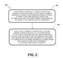
- FIG. 2is a flow diagram of a method for etching features in a film stack that may be utilized to form features on a substrate.
- FIGS. 3A and 3Bare schematic cross-sectional views of features in a film stack disposed on a substrate according to the method of FIG. 2 .
- FIG. 4(Prior Art) illustrates a schematic cross-sectional view of conventional features formed in a film stack disposed on a substrate.
- FIG. 1shows a cross-sectional view of a plasma processing system 100 that may be used to perform implementations of the present disclosure.
- Suitable processing systemsthat may be adapted for use with the implementations disclosed herein include, for example, Producer® SelectraTM Etch system available from Applied Materials, Inc. of Santa Clara, Calif.
- the plasma processing system 100generally includes a capacitively coupled plasma (CCP) unit 102 and a remote plasma source (RPS) unit 114 coupled to the CCP unit 102 .
- the plasma processing system 100may hold an internal pressure different than the outside world. For example, the pressure inside the plasma processing system 100 may be about 10 mTorr to about 20 Torr.
- the CCP unit 102functions to generate a first plasma source inside the hybrid plasma processing system 100 .
- the CCP unit 102may include a lid 106 and an ion suppression element 110 disposed relatively below the lid 106 .
- the lid 106 and the ion suppression element 110are electrically conductive electrodes that can be electrically biased with respect to each other to generate an electric field strong enough to ionize gases between the lid 106 and the ion suppression element 110 into a plasma.
- a plasma generating gas mixturemay be supplied to the CCP unit 102 from a gas source 137 through a gas inlet 107 .
- An electrical insulator 108may be disposed between the lid 106 and the ion suppression element 110 to prevent them from short circuiting when a plasma is generated.
- the exposed surfaces of the lid 106 , insulator 108 , and the ion suppression element 110generally define a plasma excitation region 112 in the CCP unit 102 .
- a power supply 140is electrically coupled to the CCP unit 102 to provide electric power to the lid 106 and/or ion suppression element 110 to generate a plasma in the plasma excitation region 112 .
- the power supply 140is operable to create an adjustable bias voltage in the ion suppression element 110 to adjust an ion concentration in the activated gas passing from the plasma excitation region 112 to the gas reaction region 130 .
- plasma generating gasesmay travel from a RPS unit 114 through a gas inlet 116 into the plasma excitation region 112 .
- the RPS unit 114functions to generate a second plasma source inside the hybrid plasma processing system 100 .
- the RPS unit 114may include a tube 117 where a plasma of ions, radicals, and electrons is generated.
- the tube 117may have a gas inlet 119 disposed at one end of the tube 117 and a gas outlet 121 disposed at the other end of the tube 117 opposing the gas inlet 119 .
- the gas inlet 119is coupled to a gas source 123 while the gas outlet 121 is in fluid communication with the plasma excitation region 112 .
- the RPS unit 114may be coupled to an energy source (not shown) to provide an excitation energy, such as an energy having a microwave frequency, to the RPS unit 114 to excite the process gas traveling from the gas source 123 into a plasma.
- the plasma generating gases from the RPS unit 114may be used to strike a plasma in the plasma excitation region 112 , or may maintain a plasma that has already been formed in the plasma excitation region 112 .
- the RPS plasma excited speciesmay include ionically-charged plasma species as well as neutral and radical species.
- the plasmamay be formed in the RPS unit 114 using a microwave, RF, or thermal approach.
- the plasma excited speciesreach the plasma excitation region 112 , they may be further excited in the CCP unit 102 , or pass through the plasma excitation region 112 without further excitation.
- plasma sourcesgenerated by, for example, an energetic excitation of gaseous molecules consisting of a plasma of charged ions, radicals, and electrons.
- an appropriate ion filter 113such as electrostatic filters, wire or mesh filters, or magnetic filters, may be used between the RPS unit 114 and the CCP unit 102 to eliminate the majority or substantially all of the ions of the plasma such that only radicals of the plasma flow through the CCP unit 102 and react with silicon or polysilicon material on the substrate, thereby obtaining a greater selectivity of processing of silicon or polysilicon material than other material (e.g., silicon oxide) on the substrate.
- the electrodes of the CCP unit 102may or may not be powered so that the radicals of the plasma from the RPS unit 114 bypass the CCP unit 102 to avoid or minimize undesired reaction occurred in
- the plasma generating gases and/or plasma excited speciesmay pass through a plurality of through holes 115 in the lid 106 for a more uniform delivery into the plasma excitation region 112 .
- the gas inlet 116is in fluid communication manner to a gas supply region 120 partitioned from the plasma excitation region 112 by the lid 106 so that the gases/species flow through the holes 115 in the lid 106 into the plasma excitation region 112 .
- the lid 106 and the ion suppression element 110may function as a first electrode and a second electrode, respectively, so that the lid 106 and/or ion suppression element 110 may receive an electric charge.
- electrical powere.g., RF power
- the hybrid plasma processing system 100may include a RF generator 140 that provides electrical power to the lid 106 and/or ion suppression element 110 .
- the electrically charged lid 106may facilitate a uniform distribution of plasma (i.e., reduce localized plasma) within the plasma excitation region 112 .
- insulator 108may electrically insulate the lid 106 and the ion suppression element 110 .
- the ion suppression element 110may include a plurality of through holes (not shown) that further suppress the migration of ionically-charged species out of the plasma excitation region 112 while allowing uncharged neutral or radical species to pass through the ion suppression element 110 into an activated gas delivery region 124 .
- Controlling the amount of ionic species passing through the ion suppression element 110provides increased control over the gas mixture brought into contact with the underlying wafer substrate, which in turn increases control of the deposition and/or etch characteristics of the gas mixture. For example, adjustments in the ion concentration of the gas mixture can significantly alter its etch selectivity (e.g., SiOx:SiNx etch ratios, Poly-Si:SiOx etch ratios, etc.).
- the showerhead 104is positioned between the ion suppression element 110 of the CCP unit 102 and a gas reaction region 130 (i.e., gas activation region) that makes contact with a substrate that may be placed on a pedestal 150 .
- the gases and plasma excited speciesmay pass through the ion suppression element 110 into an activated gas delivery region 124 that is defined between the ion suppression element 110 and the showerhead 104 .
- a portion of these gases and speciesmay further pass through the showerhead 104 into a gas reaction region 130 in which the substrate is disposed.
- the showerhead 104is a dual-zone showerhead that has a first set of channels 126 to permit the passage of plasma excited species coming from the plasma excitation region 112 , and a second set of channels 128 that deliver a second gas/precursor mixture into the gas reaction/activation region 130 .
- the first set of channels 126may traverse the thickness of the showerhead 104 .
- Each channel of the first set of channels 126may have an opening facing the gas reaction/activation region 130 , and the opening may have a smaller diameter than the diameter of the channel 126 .
- the second set of channels 128 in the showerhead 104may not traverse the thickness of the showerhead 104 . Therefore, the second set of channels 128 are not in fluid communication with the plasma excitation region 112 .
- the second set of channels 128are fluidly coupled to a source gas/precursor mixture (not shown) that is selected for the process to be performed.
- the source gas/precursor mixturemay include etchants such as fluorine based gases, oxidants, halogens, water vapor and/or carrier gases that mix in the gas reaction region 130 with plasma excited species distributed from the first set of channels 126 in the showerhead 104 .
- the two sets of channels 126 , 128prevent the plasma excited species and second gas/precursor mixture from combining until they reach the gas reaction region 130 .
- the plasma processing system 100also includes a pedestal 150 that is operable to support and move the substrate (e.g., a wafer substrate).
- the pedestalmay be vertically or axially adjustable within the processing chamber 100 to increase or decrease distance between the pedestal 150 and the showerhead 104 , which defines the gas reaction region 130 .
- the pedestal 150may have a heat exchange channel through which a heat exchange fluid (e.g., water) flows to control the temperature of the wafer substrate. Circulation of the heat exchange fluid allows the substrate temperature to be maintained at relatively low temperatures (e.g., about ⁇ 20° C. to about 90° C.).
- the pedestal 150may also be configured with a heating element (such as a resistive heating element) embedded therein to maintain the substrate at desired heating temperatures (e.g., about 90° C. to about 1100° C.).
- the plasma excited speciesmay be generated by the CCP unit 102 alone, the RPS unit 114 alone, or both.
- the CCP unit 102may serve as a primary plasma source while the RPS unit 114 may serve as a secondary plasma source, or vice versa, depending upon the process scheme.
- both CCP unit 102 and RPS unit 114may be used to generate plasma excited species so that some power burden is shifted from the CCP unit 102 to the RPS unit 114 , which allows the CCP unit 102 to operate at lower power, thereby reducing ion bombardment of the powered electrode in the CCP to a lesser extent.
- FIG. 2is a flow diagram of a method 200 for etching features in a film stack that may be utilized to form features on a substrate.
- the method 200may be performed in a processing system, such as the plasma processing system 100 depicted in FIG. 1 or other suitable processing chambers.
- FIGS. 3A and 3Bare schematic cross-sectional views of features in a film stack disposed on a substrate according to some implementations of the method 200 .
- the method 200may be utilized to etch high aspect ratio features, e.g., greater than 10:1, for semiconductor devices, particularly for three dimensional (3D) stacking of semiconductor memory.
- the method 200is described below with reference to a substrate utilized to manufacture features in a film stack that may be utilized to form stair-like structures for three dimensional semiconductor chips, the method 200 may also be used to advantage in other applications for manufacturing other types of devices.
- the method 200begins at block 202 by transferring a substrate, such as a substrate 400 depicted in FIG. 3A , onto a substrate support pedestal assembly disposed in a processing chamber, such as the pedestal 150 of the processing chamber 200 depicted in FIG. 1 .
- the substrate 300has a film stack 302 formed thereon.
- the substrate 300may be a silicon based material or any suitable insulating materials or conductive materials as needed.
- the film stack 302may be utilized to form a gate structure, a contact structure or an interconnection structure in the front end or back end processes.
- the substrate 300may be a material such as crystalline silicon (e.g., Si ⁇ 100> or Si ⁇ 111>), silicon oxide, strained silicon, silicon germanium, doped or undoped polysilicon, doped or undoped silicon wafers and patterned or non-patterned wafers silicon on insulator (SOI), carbon doped silicon oxides, silicon nitride, doped silicon, germanium, gallium arsenide, glass, sapphire.
- the substrate 300may have various dimensions, such as 200 mm, 300 mm, 450 mm or other diameter wafers, as well as, rectangular or square panels. Unless otherwise noted, implementations and examples described herein are conducted on substrates with a 200 mm diameter, a 300 mm diameter, a 450 mm diameter substrate.
- the substrate 300may include a buried dielectric layer disposed on a silicon crystalline substrate. In the example depicted herein, the substrate 300 is a crystalline silicon substrate.
- the film stack 302 disposed on the substrate 300has a multi-material layer 304 that has a number of vertically stacked layers.
- the multi-material layer 304may include pairs of layers, for example a stack of first layers (shown as 304 a 1 , 304 a 2 , . . . , 304 a n ) and a stack of second layers (shown as 304 b 1 , 304 b 2 , . . . , 304 b n ) repeatedly formed over the substrate 300 .
- the multi-material layer 304includes alternating layers of the first layer (shown as 304 a 1 , 304 a 2 , . . . , 304 a n ) and the second layer (shown as 304 b 1 , 304 b 2 , . . . , 304 b n ) repeatedly formed over the substrate 300 .
- the multi-material layer 304 formed in the film stack 302may be a part of a semiconductor chip, such as a three-dimensional (3D) memory chip.
- FIG. 3Ashows three repeating layers of first layers (shown as 304 a 1 , 304 a 2 , . . . , 304 a n ) and second layers (shown as 304 b 1 , 304 b 2 , . . . , 304 b n ) alternately laminated on the substrate 300 , any desired number of repeating pairs comprised of first and the second layers may be utilized as needed.
- the multi-material layer 304may be utilized to form multiple gate structures for a three-dimensional (3D) memory chip.
- the first layers 304 a 1 , 304 a 2 , . . . , 304 a n , formed in the multi-material layer 304may be a first dielectric layer and the second layers 304 b 1 , 304 b 2 , . . . , 304 b n may be a second dielectric layer.
- Suitable dielectric layersmay be utilized to form the first layers 304 a 1 , 304 a 2 , . . . , 304 a n and the second layers 304 b 1 , 304 b 2 , . . .
- the first layers 304 a 1 , 304 a 2 , . . . , 304 a nis silicon oxide and the second layers 304 b 1 , 304 b 2 , . . . , 304 b n is silicon nitride.
- the first layers 304 a 1 , 304 a 2 , . . . , 304 a nis silicon oxynitride and the second layers 304 b 1 , 304 b 2 , . . . , 304 b n is silicon oxycarbide.
- the first layers 304 a 1 , 304 a 2 , . . . , 304 a n and/or second layers 304 b 1 , 304 b 2 , . . . , 304 b nmay be formed from a high-k material having a dielectric constant greater than 4.
- Suitable examples of the high-k materialsinclude hafnium dioxide (HfO 2 ), zirconium dioxide (ZrO 2 ), hafnium silicon oxide (HfSiO 2 ), hafnium aluminum oxide (HfAlO), zirconium silicon oxide (ZrSiO2), tantalum dioxide (TaO 2 ), aluminum oxide, aluminum doped hafnium dioxide, bismuth strontium titanium (BST), and platinum zirconium titanium (PZT), among others.
- 304 a nmay be a dielectric layer such as silicon oxide, silicon nitride, silicon oxynitride, silicon carbide, silicon oxycarbide, composite of oxide and nitride mentioned above, and the second layers 304 b 1 , 304 b 2 , . . . , 304 b n may be a high-k material discussed above, or vice versa.
- the first layers 304 a 1 , 304 a 2 , . . . , 304 a , and the second layers 304 b 1 , 304 b 2 , . . . , 304 b nmay be a conductive layer selected from a group consisting of doped silicon, such as n-type or p-type doped silicon, other suitable silicon containing material, tungsten (W), tungsten silicide (WSi), tungsten polysilicon (W/poly), tungsten alloy, tantalum (Ta), titanium (Ti), copper (Cu), ruthenium (Ru), nickel (Ni), cobalt (Co), chromium (Cr), iron (Fe), manganese (Mn), aluminum (Al), hafnium (Hf), vanadium (V), molybdenum (Mo), palladium (Pd), gold (Au), silver (Au), platinum (Pt), alloys thereof, nitride compound
- the first layers 304 a 1 , 304 a 2 , . . . , 304 a nis W and the second layers 304 b 1 , 304 b 2 , . . . , 304 b n is TiN.
- the first layers 304 a 1 , 304 a 2 , . . . , 304 a nis W and the second layers 304 b 1 , 304 b 2 , . . . , 304 b n is TaN.
- the first layers 304 a 1 , 304 a 2 , . . . , 304 a nare silicon oxide layers and the second layers 304 b 1 , 304 b 2 , . . . , 304 b n are silicon nitride layers or polysilicon layers disposed on the first layers 304 a 1 , 304 a 2 , . . . , 304 a n .
- 304 a nmay be controlled at between about 50 ⁇ and about 1000 ⁇ , such as about 500 ⁇ , and the thickness of the each second layers 304 b 1 , 304 b 2 , . . . , 304 b n may be controlled at between about 50 ⁇ and about 1000 ⁇ , such as about 500 ⁇ .
- the multi-material layers 304may have a total thickness between about 100 ⁇ and about 2000 ⁇ .
- an etching gas mixtureis supplied into a remote plasma source (RPS) unit of the processing system, such as the RPS unit 114 of FIG. 1 .
- the etching gas mixturecan be excited in the RPS unit 114 using a microwave, RF, or thermal approach.
- the etching gas mixtureis excited using a RF power applied at a high frequency, such as greater than 2.5 MHz.
- the plasma excited speciesare then flowed to the plasma excitation region 112 , where they may be further excited in the CCP unit 102 , or pass through the plasma excitation region 112 without further excitation.
- radicals of a plasmaare desired (as they react in a much more desirable manner with silicon or polysilicon material on a substrate than ions or a mixture of radicals and ions)
- the majority or substantially all of the ions of the plasmamay be eliminated using an ion filter, such as the ion filter 113 shown in FIG. 1 .
- an ion filtersuch as the ion filter 113 shown in FIG. 1 .
- first layer materiale.g., 304 a 1 , 304 a 2 , . . . , 304 a n
- other materiale.g., second layers 304 b 1 , 304 b 2 , . . . , 304 b n
- the plasma excited species or radicalsare used to etch portions of the multi-material layers 304 , using a patterned photoresist layer (not shown) as a mask. The etching may be continued until a predetermined depth of a feature 314 is formed in the multi-material layer 304 .
- the feature 314may be a contact hole, via, trench or any structure with a desired profile.
- FIG. 3Ashows one embodiment where the multi-material layer 304 has features 314 formed through the first layers 304 a 1 , 304 a 2 , . . . , 304 a n and the second layers 304 b 1 , 304 b 2 , . . . , 304 b n , thereby exposing the top surface of the substrate 300 .
- the etching gas mixture selected to etch the multi-material layer 304includes at least a fluorine-containing chemistry.
- Suitable examples of the fluorine-containing chemistryinclude NF 3 , XeF 2 , ClF, ClF 3 , ClF 5 , and F 2 , and the like.
- the etching gas mixturemay use a fluorine-carbon containing gas having a formula C x F y , wherein x and y are integers ranging from 1 to 8 and 8 to 34 respectively.
- Suitable examples of the fluorine-carbon containing gasmay include CF 4 , C 2 F 6 , C 3 F 6 , C 4 F 6 , C 4 F 8 , C 5 F 10 , C 6 F 8 , and the like.
- the fluorine-containing chemistry in the etching gas mixtureincludes NF 3 .
- other halogen containing gas, SF 6 , Cl 2 , Br 2 , HCl, and the like,may also be supplied into the etching gas mixture during etching.
- a RF bias powermay be optionally provided to the substrate to provide directionality to the plasma or radicals to enhance selectivity for removal of target materials from the multi-material layer 304 .
- the RF bias powermay be provided at a power level of about 50 W to about 300 W (300 mm substrate) and a low frequency, such as less than 2.5 MHz, for example about 300 kHz to 2 MHz.
- the etching gas mixturemay be maintained at a flow rate by volume between about 20 sccm and about 500 sccm.
- the processing systemmay be maintained at a pressure of about 2 Torr and about 20 Torr, such as about 8 Torr to about 10 Torr.
- the temperature of the processing systemmay be maintained at about ⁇ 100° C.
- etching at higher pressure and lower temperatureensures a better top to bottom loading (i.e., amount of target materials consumed at top portion versus bottom portion).
- Etching at lower temperaturemay be advantageous because surface reaction rate is decreased exponentially. In cases where the target layers are W, Si, or SiN, it has been observed that controlling surface reaction rate will help achieve a better top to bottom loading.
- the plasma excited species or radicals of the fluorine-containing chemistryfor example NF 3
- F 2 speciesetch target materials (e.g., W/TiN or SiN etc.) at a speed relatively faster than SiO, adequate etching selectivity of materials can be obtained. Therefore, a highly uniform recess etch of target materials throughout the entire multi-material layer 304 is achieved.
- the top portion of the feature 314may be selectively covered with a passivation layer 316 while the bottom portion of the feature 314 is free from the passivation layer.
- the passivation layer 316is formed on exposed surfaces at the top portion of the multi-material layer 304 to protect the top portion of the features 314 from being overly etched and attached during the early stages of the etch process.
- the top portion of the features 314 in this disclosuremay generally refer to at least first layers 304 a 1 and 304 a 2 and second layers 304 b 1 and 304 b 2 .
- a ratio of the coverage of the passivation layer 316 to a depth of the feature 314may be about 1:2 to about 1:8, such as about 1:3 to about 1:5.
- the top portion of the features 314which would have been overly etched due to longer exposure to the etching chemistry, will now be etched at a slower rate matching the etching rate at the bottom portion of the features 314 .
- proper critical dimension throughout the length of the features 314is obtained.
- the passivation layer 316is formed conformally or substantially conformally on the sidewalls of the top portion of the features 314 , it is contemplated that the passivation layer 316 may also be formed on the sidewalls of the bottom portion of the features 314 , depending on the target material to be removed and/or the etching chemistry used.
- the passivation layer 316may be formed from the same material as the underneath material that is covered by the passivation layer 316 .
- the passivation layer 316protects the top portion with a material identical to the underlying material to have the top and bottom etch rate equal.
- the material of the passivation layer 316can be Si based material comprising Si, N, O, C, and H.
- the passivation layer 316may be any suitable carbon doped Si x O y N z H w material, wherein x, y, z, and w can be all integers such that x+y+z+w is greater than zero.
- the material of the passivation layer 316can be W based material comprising W, N, O, C, and H.
- the passivation layer 316may be any suitable carbon doped W x O y N z H w material, wherein x, y, z, and w can be all integers such that x+y+z+w is greater than zero.
- the material of the passivation layer 316can be Ti based material comprising Ti, N, O, C, and H.
- the passivation layer 316may be any suitable carbon doped Ti x O y N z H w material, wherein x, y, z, and w can be all integers such that x+y+z+w is greater than zero.
- the material of the passivation layer 316can be Ta based material comprising Ta, N, O, C, and H.
- the passivation layer 316may be any suitable carbon doped Ta x O y N z H w material, wherein x, y, z, and w can be all integers such that x+y+z+w is greater than zero.
- the passivation layer 316may be formed either thermally or with in-situ plasma.
- a RF bias powermay be optionally used to enhance formation of the passivation layer 316 .
- the RF bias powermay be provided at a power level of about 50 W to about 300 W (300 mm substrate) and a low frequency, such as less than 2.5 MHz, for example about 300 kHz to 2 MHz.
- the top portion of the features 314may be subjected to a pre-treatment process to make it less reactive with the subsequent plasma excited species or radicals of the etching chemistry. Therefore, the bottom portion of the features 314 will be etched faster than the top portion of the features 314 in a subsequent stage.
- the top portion of the features 314may be oxidized so that the top portion is reacted with the etching species or radicals at a much slower rate than the bottom portion of the features 314 . This is because F 2 species or radicals react with oxides (e.g., tungsten oxides or silicon oxides) at a relatively slower rate than the silicon nitrides or silicon.
- the oxidized top portion of the features 314is etched at the same rate or an etching rate that is slightly slower the bottom portion of the features 314 which is not oxidized by the pre-treatment process, it is possible to achieve uniform profile and proper critical dimension of the feature 314 formed in the multi-material layer 304 .
- the thickness of the oxide layer 318may be gradually reduced along the depth of the features 314 , as shown in FIG. 3B . In some cases, the thickness of the oxide layer 318 at or around the middle portion of the features 314 is reduced to zero after oxidization.
- a ratio of the coverage of the oxide layer 318 (i.e., oxidized region) to a depth of the feature 314may be about 1:2 to about 1:8, such as about 1:3 to about 1:5.
- an oxygen-containing gasis supplied to assist in oxidizing of the top portion of the features 314 .
- the pre-treatment processcan include plasma treatment or thermal treatment, with inert gases or active gases such as hydrogen, oxygen, or nitrogen.
- Examples of the inert gas supplied in the gas mixtureinclude Ar, He, Ne, Kr, Xe or the like.
- Suitable examples of the oxygen-containing gasmay be species or radicals of O 2 , NO 2 , N 2 O, CO, CO 2 , H 2 O 2 , O 3 , and the like.
- the oxygen-containing gasmay be flowed into the gas reaction region 130 at a first flow rate, which can be any suitable flowing rate, for example about 20 sccm and about 2500 sccm, such as about 80 sccm to about 500 sccm.
- Plasma excited species or radicals of the fluorine-containing chemistrymay or may not be introduced into the gas reaction region 130 at this stage.
- the chamber pressuremay be maintained at a pressure of about 1 Torr to control the oxidization occurring mainly at the top portion of the features 314 .
- the flow of the oxygen-containing gasis turned off and the chamber pressure is raised to about 5 Torr to 20 Torr, for example about 7 Torr to 8 Torr.
- the etching species or radicals as discussed abovemay then be introduced into the gas reaction region 130 of the processing system to etch the lower portion of the feature 314 .
- the etching species or radicalsmay be flowed into the gas reaction region 130 at a second flow rate that is slower than the first flowing rate of the oxygen-containing gas. Due to the presence of the oxidization layer 318 , the top portion of the features 314 will be etched at a slower etching rate than the lower portion. As a result, a uniform profile and proper critical dimension throughout the features 314 is obtained.
- a post-treatment processcan be performed after etching process and/or the pre-treatment process to help top to bottom loading by driving out all etch by-products generated during the etch process from both top and bottom portions of the features 314 .
- the post-treatment processuses a purging gas to remove fluorine residues or fluoride, oxides or oxyfluorides of tungsten at the sidewalls or the bottom of the features 314 , which may otherwise result in early close-up of the features 314 being formed in the multi-material layer 304 and thus preventing etching through the entire film stack 304 to expose the substrate 300 .
- the purging gasmay include an inert gas such as helium or argon.
- the purging gasmay optionally include an oxygen gas, hydrogen gas, or a nitrogen gas.
- the purging gasmay be supplied to the processing system at a flow rate by volume of between about 20 sccm and about 12500 sccm, such as about 100 sccm to about 2000 sccm, for example about 550 sccm to about 1200 sccm, to drive etch by-products out of the features 314 .
- the post-treatment processmay be performed for about 15 seconds to about 60 seconds, for example about 30 seconds.
- Benefits of the present disclosureinclude improved etch processes for uniformly recessing a sidewall of high aspect ratio features (e.g., trenches or contact holes) of 3D NAND that has alternating layers of conductive layers or insulating layers by exposing the sidewall of the features to a remote plasma formed from F-based chemistry at low temperature and high pressure conditions to achieve 1:1 top to bottom loading (i.e., amount of target materials consumed at top portion versus bottom portion).
- the top portion of the sidewallcan be selectively covered with a passivation layer to ensure proper critical dimension throughout the length of the features.
- the top portion of the sidewallcan be treated before the etch process to make it less reactive with the subsequent plasma excited species or radicals of the etching chemistry than the lower portion, which in turn results in better top to bottom loading.
- chemistry-based isotropic etch processes and passivation/treatmentshelp form high aspect ratio features with accurate and uniform profiles for three dimensional (3D) stacking of semiconductor chips. As a result, lower process cost, better process repeatability and minimized environment impact can be obtained.
Landscapes
- Engineering & Computer Science (AREA)
- Physics & Mathematics (AREA)
- Chemical & Material Sciences (AREA)
- Computer Hardware Design (AREA)
- General Physics & Mathematics (AREA)
- Microelectronics & Electronic Packaging (AREA)
- Power Engineering (AREA)
- Condensed Matter Physics & Semiconductors (AREA)
- Manufacturing & Machinery (AREA)
- Chemical Kinetics & Catalysis (AREA)
- General Chemical & Material Sciences (AREA)
- Plasma & Fusion (AREA)
- Inorganic Chemistry (AREA)
- Ceramic Engineering (AREA)
- Drying Of Semiconductors (AREA)
- Semiconductor Memories (AREA)
Abstract
Description
- This application claims priority to U.S. provisional patent application Ser. No. 62/439,785, filed Dec. 28, 2016, and U.S. provisional patent application Ser. No. 62/439,416, filed Dec. 27, 2016, which are herein incorporated by reference.
- Embodiments of the present disclosure generally relate to methods of forming high aspect ratio features in a vertical type semiconductor device.
- The growing demands of mobile computing and data centers continue to drive the need for high-capacity, high-performance NAND flash technology. With planar NAND nearing its practical scaling limits, NAND flash memory has moved from a planar configuration to a vertical configuration (VNAND). This vertical configuration permits the memory devices to be formed at significantly greater bit density. In manufacturing stacking of 3D semiconductor chips, stair-like structures are often utilized to allow multiple interconnection structures to be disposed thereon, forming high-density of vertical transistor devices.
- When forming features, such as trenches or vias, in stair-like structures in a film stack disposed on a substrate, an etch process using a photoresist layer as an etching mask is often utilized. The film stack typically includes multiple material layers in which the features, such as trenches or contact holes, are formed with high aspect ratios. High aspect ratio is generally defined as the ratio between the depth of the feature and the width of the feature, for at least about 20:1 and greater. In an exemplary embodiment depicted in
FIG. 4 (Prior Art), a photoresist layer (not shown) may serve as an etching mask layer to transfer structures onto afilm stack 400 disposed on asubstrate 404 to form stair-like structures 410 on thesubstrate 404. Thefilm stack 300 typically includes alternating layers of layers402a,402b(shown as402a1,402b1,402a2,402b2, . . . ,402n1,402n2), either conductive layers or insulating layers. For example, the film stack may include alternating layers of SiO2/Si, SiO/SiN, SiO2/W, or W/TiN with thickness up to several microns. One of these two materials needs to be etched or recessed selectively within the contact holes to form memory cells. - During etching, features430 with high aspect ratio, such as greater than about 5:1 or above, for example about 10:1 or above, may be formed into the
film stack 400. Due to the high aspect ratio, however, it has been challenging for traditional plasma dry etch or wet etch to etch the sidewall W/TiN Si, or SiN uniformly from the top portion of the contact holes to the bottom portion of the contact holes, causing greater recessing of the material, for example tungsten, near the top portion of the contact holes than at the bottom portion (i.e., irregular dimensional profiles of the etched structures). In addition, redeposition or build-up of by-products or other materials generated during the etch process may accumulate and/or attach on the top and/or sidewalls of thefeatures feature film stack 400 and thus preventing etching through theentire film stack 400. Moreover, as the opening of theetched features 432 are narrowed and/or sealed by the accumulated redeposition material, the reactive etchants are prevented from reaching thelower surface 433 of thefeatures 432, thereby limiting the aspect ratio that may be obtained. - Thus, there is a need for improved methods for forming high aspect ratio features, such as forming features in stair-like structures, with accurate profiles and dimension control for three dimensional (3D) stacking of semiconductor chips.
- Embodiments of the present disclosure provide methods for forming features in a film stack that may be utilized to form stair-like structures with accurate profiles control in manufacturing three dimensional (3D) stacking of semiconductor chips. In one embodiment, a method includes exposing a substrate having a multi-material layer formed thereon to radicals of a remote plasma to form one or more features through the multi-material layer, the one or more features exposing a portion of a top surface of the substrate, and the multi-material layer comprising alternating layers of a first layer and a second layer, wherein the remote plasma is formed from an etching gas mixture comprising a fluorine-containing chemistry, and wherein the process chamber is maintained at a pressure of about 2 Torr to about 20 Torr and a temperature of about −100° C. to about 100° C.
- In another embodiment, a structure is provided. The structure includes a substrate having a multi-material layer formed thereon, the multi-material layer comprising alternating layers of a first layer and a second layer, one or more features formed through the multi-material layer to expose a portion of a top surface of the substrate, and a passivation layer formed on exposed surfaces of a top portion of the one or more features, wherein a ratio of the coverage of the passivation layer to a depth of the features is 1:2 to about 1:8.
- In yet another embodiment, a method includes exposing a substrate having a multi-material layer formed thereon to radicals of a remote plasma to form one or more features through the multi-material layer, the one or more features exposing a portion of a top surface of the substrate, and the multi-material layer comprising alternating layers of a first layer and a second layer, and exposing exposed surfaces of a top portion of the one or more features to an oxygen-containing gas to oxidize the exposed surfaces of the top portion, wherein a ratio of the coverage of the oxidized surfaces to a depth of the features is 1:2 to about 1:8, and purging the process chamber.
- Implementations of the present disclosure, briefly summarized above and discussed in greater detail below, can be understood by reference to the illustrative implementations of the disclosure depicted in the appended drawings. It is to be noted, however, that the appended drawings illustrate only typical implementations of this disclosure and are therefore not to be considered limiting of its scope, for the disclosure may admit to other equally effective implementations.
FIG. 1 shows a cross-sectional view of aplasma processing system 100 that may be used to perform implementations of the present disclosure.FIG. 2 is a flow diagram of a method for etching features in a film stack that may be utilized to form features on a substrate.FIGS. 3A and 3B are schematic cross-sectional views of features in a film stack disposed on a substrate according to the method ofFIG. 2 .FIG. 4 (Prior Art) illustrates a schematic cross-sectional view of conventional features formed in a film stack disposed on a substrate.- To facilitate understanding, identical reference numerals have been used, where possible, to designate identical elements that are common to the figures. The figures are not drawn to scale and may be simplified for clarity. It is contemplated that elements and features of one implementation may be beneficially incorporated in other implementations without further recitation.
FIG. 1 shows a cross-sectional view of aplasma processing system 100 that may be used to perform implementations of the present disclosure. Suitable processing systems that may be adapted for use with the implementations disclosed herein include, for example, Producer® Selectra™ Etch system available from Applied Materials, Inc. of Santa Clara, Calif. Theplasma processing system 100 generally includes a capacitively coupled plasma (CCP)unit 102 and a remote plasma source (RPS)unit 114 coupled to theCCP unit 102. Theplasma processing system 100 may hold an internal pressure different than the outside world. For example, the pressure inside theplasma processing system 100 may be about 10 mTorr to about 20 Torr.- The
CCP unit 102 functions to generate a first plasma source inside the hybridplasma processing system 100. TheCCP unit 102 may include alid 106 and anion suppression element 110 disposed relatively below thelid 106. In some implementations, thelid 106 and theion suppression element 110 are electrically conductive electrodes that can be electrically biased with respect to each other to generate an electric field strong enough to ionize gases between thelid 106 and theion suppression element 110 into a plasma. A plasma generating gas mixture may be supplied to theCCP unit 102 from agas source 137 through agas inlet 107. Anelectrical insulator 108 may be disposed between thelid 106 and theion suppression element 110 to prevent them from short circuiting when a plasma is generated. The exposed surfaces of thelid 106,insulator 108, and theion suppression element 110 generally define aplasma excitation region 112 in theCCP unit 102. - A
power supply 140 is electrically coupled to theCCP unit 102 to provide electric power to thelid 106 and/orion suppression element 110 to generate a plasma in theplasma excitation region 112. Thepower supply 140 is operable to create an adjustable bias voltage in theion suppression element 110 to adjust an ion concentration in the activated gas passing from theplasma excitation region 112 to thegas reaction region 130. In one implementation, plasma generating gases may travel from aRPS unit 114 through agas inlet 116 into theplasma excitation region 112. TheRPS unit 114 functions to generate a second plasma source inside the hybridplasma processing system 100. TheRPS unit 114 may include atube 117 where a plasma of ions, radicals, and electrons is generated. Thetube 117 may have agas inlet 119 disposed at one end of thetube 117 and agas outlet 121 disposed at the other end of thetube 117 opposing thegas inlet 119. Thegas inlet 119 is coupled to agas source 123 while thegas outlet 121 is in fluid communication with theplasma excitation region 112. TheRPS unit 114 may be coupled to an energy source (not shown) to provide an excitation energy, such as an energy having a microwave frequency, to theRPS unit 114 to excite the process gas traveling from thegas source 123 into a plasma. The plasma generating gases from theRPS unit 114 may be used to strike a plasma in theplasma excitation region 112, or may maintain a plasma that has already been formed in theplasma excitation region 112. The RPS plasma excited species may include ionically-charged plasma species as well as neutral and radical species. - The plasma may be formed in the
RPS unit 114 using a microwave, RF, or thermal approach. When the plasma excited species reach theplasma excitation region 112, they may be further excited in theCCP unit 102, or pass through theplasma excitation region 112 without further excitation. - In general, plasma sources generated by, for example, an energetic excitation of gaseous molecules consisting of a plasma of charged ions, radicals, and electrons. In some processes where radicals of a plasma are desirable (as they react in a much more desirable manner with silicon or polysilicon material on a substrate than ions or a mixture of radicals and ions), an
appropriate ion filter 113, such as electrostatic filters, wire or mesh filters, or magnetic filters, may be used between theRPS unit 114 and theCCP unit 102 to eliminate the majority or substantially all of the ions of the plasma such that only radicals of the plasma flow through theCCP unit 102 and react with silicon or polysilicon material on the substrate, thereby obtaining a greater selectivity of processing of silicon or polysilicon material than other material (e.g., silicon oxide) on the substrate. The electrodes of theCCP unit 102 may or may not be powered so that the radicals of the plasma from theRPS unit 114 bypass theCCP unit 102 to avoid or minimize undesired reaction occurred in theplasma excitation region 112. - The plasma generating gases and/or plasma excited species may pass through a plurality of through
holes 115 in thelid 106 for a more uniform delivery into theplasma excitation region 112. Thegas inlet 116 is in fluid communication manner to agas supply region 120 partitioned from theplasma excitation region 112 by thelid 106 so that the gases/species flow through theholes 115 in thelid 106 into theplasma excitation region 112. - As noted above, the
lid 106 and theion suppression element 110 may function as a first electrode and a second electrode, respectively, so that thelid 106 and/orion suppression element 110 may receive an electric charge. In these configurations, electrical power (e.g., RF power) may be applied to thelid 106,ion suppression element 110, or both. For example, electrical power may be applied to thelid 106 while theion suppressor 110 is grounded. The hybridplasma processing system 100 may include aRF generator 140 that provides electrical power to thelid 106 and/orion suppression element 110. The electrically chargedlid 106 may facilitate a uniform distribution of plasma (i.e., reduce localized plasma) within theplasma excitation region 112. To enable formation of a plasma in theplasma excitation region 112,insulator 108 may electrically insulate thelid 106 and theion suppression element 110. - The
ion suppression element 110 may include a plurality of through holes (not shown) that further suppress the migration of ionically-charged species out of theplasma excitation region 112 while allowing uncharged neutral or radical species to pass through theion suppression element 110 into an activated gas delivery region124. Controlling the amount of ionic species passing through theion suppression element 110 provides increased control over the gas mixture brought into contact with the underlying wafer substrate, which in turn increases control of the deposition and/or etch characteristics of the gas mixture. For example, adjustments in the ion concentration of the gas mixture can significantly alter its etch selectivity (e.g., SiOx:SiNx etch ratios, Poly-Si:SiOx etch ratios, etc.). - The
showerhead 104 is positioned between theion suppression element 110 of theCCP unit 102 and a gas reaction region130 (i.e., gas activation region) that makes contact with a substrate that may be placed on apedestal 150. The gases and plasma excited species may pass through theion suppression element 110 into an activated gas delivery region124 that is defined between theion suppression element 110 and theshowerhead 104. A portion of these gases and species may further pass through theshowerhead 104 into agas reaction region 130 in which the substrate is disposed. - In one implementation, the
showerhead 104 is a dual-zone showerhead that has a first set ofchannels 126 to permit the passage of plasma excited species coming from theplasma excitation region 112, and a second set ofchannels 128 that deliver a second gas/precursor mixture into the gas reaction/activation region 130. The first set ofchannels 126 may traverse the thickness of theshowerhead 104. Each channel of the first set ofchannels 126 may have an opening facing the gas reaction/activation region 130, and the opening may have a smaller diameter than the diameter of thechannel 126. The second set ofchannels 128 in theshowerhead 104 may not traverse the thickness of theshowerhead 104. Therefore, the second set ofchannels 128 are not in fluid communication with theplasma excitation region 112. Instead, the second set ofchannels 128 are fluidly coupled to a source gas/precursor mixture (not shown) that is selected for the process to be performed. When theplasma processing system 100 is configured to perform an etch on the substrate surface, the source gas/precursor mixture may include etchants such as fluorine based gases, oxidants, halogens, water vapor and/or carrier gases that mix in thegas reaction region 130 with plasma excited species distributed from the first set ofchannels 126 in theshowerhead 104. The two sets ofchannels gas reaction region 130. - The
plasma processing system 100 also includes apedestal 150 that is operable to support and move the substrate (e.g., a wafer substrate). The pedestal may be vertically or axially adjustable within theprocessing chamber 100 to increase or decrease distance between thepedestal 150 and theshowerhead 104, which defines thegas reaction region 130. Thepedestal 150 may have a heat exchange channel through which a heat exchange fluid (e.g., water) flows to control the temperature of the wafer substrate. Circulation of the heat exchange fluid allows the substrate temperature to be maintained at relatively low temperatures (e.g., about −20° C. to about 90° C.). Thepedestal 150 may also be configured with a heating element (such as a resistive heating element) embedded therein to maintain the substrate at desired heating temperatures (e.g., about 90° C. to about 1100° C.). - By combining a
RPS unit 114 with aCCP unit 102, the plasma excited species may be generated by theCCP unit 102 alone, theRPS unit 114 alone, or both. TheCCP unit 102 may serve as a primary plasma source while theRPS unit 114 may serve as a secondary plasma source, or vice versa, depending upon the process scheme. In cases where the process requires higher power input (550W or above), bothCCP unit 102 andRPS unit 114 may be used to generate plasma excited species so that some power burden is shifted from theCCP unit 102 to theRPS unit 114, which allows theCCP unit 102 to operate at lower power, thereby reducing ion bombardment of the powered electrode in the CCP to a lesser extent. FIG. 2 is a flow diagram of amethod 200 for etching features in a film stack that may be utilized to form features on a substrate. Themethod 200 may be performed in a processing system, such as theplasma processing system 100 depicted inFIG. 1 or other suitable processing chambers.FIGS. 3A and 3B are schematic cross-sectional views of features in a film stack disposed on a substrate according to some implementations of themethod 200. Themethod 200 may be utilized to etch high aspect ratio features, e.g., greater than 10:1, for semiconductor devices, particularly for three dimensional (3D) stacking of semiconductor memory. Although themethod 200 is described below with reference to a substrate utilized to manufacture features in a film stack that may be utilized to form stair-like structures for three dimensional semiconductor chips, themethod 200 may also be used to advantage in other applications for manufacturing other types of devices.- The
method 200 begins atblock 202 by transferring a substrate, such as asubstrate 400 depicted inFIG. 3A , onto a substrate support pedestal assembly disposed in a processing chamber, such as thepedestal 150 of theprocessing chamber 200 depicted inFIG. 1 . Thesubstrate 300 has afilm stack 302 formed thereon. Thesubstrate 300 may be a silicon based material or any suitable insulating materials or conductive materials as needed. Thefilm stack 302 may be utilized to form a gate structure, a contact structure or an interconnection structure in the front end or back end processes. Thesubstrate 300 may be a material such as crystalline silicon (e.g., Si<100> or Si<111>), silicon oxide, strained silicon, silicon germanium, doped or undoped polysilicon, doped or undoped silicon wafers and patterned or non-patterned wafers silicon on insulator (SOI), carbon doped silicon oxides, silicon nitride, doped silicon, germanium, gallium arsenide, glass, sapphire. Thesubstrate 300 may have various dimensions, such as 200 mm, 300 mm, 450 mm or other diameter wafers, as well as, rectangular or square panels. Unless otherwise noted, implementations and examples described herein are conducted on substrates with a 200 mm diameter, a 300 mm diameter, a 450 mm diameter substrate. In the implementation wherein a SOI structure is utilized for thesubstrate 300, thesubstrate 300 may include a buried dielectric layer disposed on a silicon crystalline substrate. In the example depicted herein, thesubstrate 300 is a crystalline silicon substrate. - In one implementation, the
film stack 302 disposed on thesubstrate 300 has amulti-material layer 304 that has a number of vertically stacked layers. Themulti-material layer 304 may include pairs of layers, for example a stack of first layers (shown as304a1,304a2, . . . ,304an) and a stack of second layers (shown as304b1,304b2, . . . ,304bn) repeatedly formed over thesubstrate 300. In one embodiment, themulti-material layer 304 includes alternating layers of the first layer (shown as304a1,304a2, . . . ,304an) and the second layer (shown as304b1,304b2, . . . ,304bn) repeatedly formed over thesubstrate 300. - The
multi-material layer 304 formed in thefilm stack 302 may be a part of a semiconductor chip, such as a three-dimensional (3D) memory chip. AlthoughFIG. 3A shows three repeating layers of first layers (shown as304a1,304a2, . . . ,304an) and second layers (shown as304b1,304b2, . . . ,304bn) alternately laminated on thesubstrate 300, any desired number of repeating pairs comprised of first and the second layers may be utilized as needed. - In one implementation, the
multi-material layer 304 may be utilized to form multiple gate structures for a three-dimensional (3D) memory chip. Thefirst layers multi-material layer 304 may be a first dielectric layer and the second layers304b1,304b2, . . . ,304bnmay be a second dielectric layer. Suitable dielectric layers may be utilized to form thefirst layers first layers first layers - In some embodiments, the
first layers first layers - In some examples, the
first layers first layers first layers - In one exemplary example, the
first layers first layers first layers multi-material layers 304 may have a total thickness between about 100 Å and about 2000 Å. - At
block 204, an etching gas mixture is supplied into a remote plasma source (RPS) unit of the processing system, such as theRPS unit 114 ofFIG. 1 . The etching gas mixture can be excited in theRPS unit 114 using a microwave, RF, or thermal approach. In one implementation, the etching gas mixture is excited using a RF power applied at a high frequency, such as greater than 2.5 MHz. The plasma excited species are then flowed to theplasma excitation region 112, where they may be further excited in theCCP unit 102, or pass through theplasma excitation region 112 without further excitation. In some cases where radicals of a plasma are desired (as they react in a much more desirable manner with silicon or polysilicon material on a substrate than ions or a mixture of radicals and ions), the majority or substantially all of the ions of the plasma may be eliminated using an ion filter, such as theion filter 113 shown inFIG. 1 . As a result, only radicals of the plasma flow through theCCP unit 102 and react with target material on the substrate, thereby obtaining a greater selectivity of processing of first layer material (e.g.,304a1,304a2, . . . ,304an) than other material (e.g., second layers304b1,304b2, . . . ,304bn) in themulti-material layers 304. - The plasma excited species or radicals are used to etch portions of the
multi-material layers 304, using a patterned photoresist layer (not shown) as a mask. The etching may be continued until a predetermined depth of afeature 314 is formed in themulti-material layer 304. Thefeature 314 may be a contact hole, via, trench or any structure with a desired profile.FIG. 3A shows one embodiment where themulti-material layer 304 hasfeatures 314 formed through thefirst layers substrate 300. - In one embodiment, the etching gas mixture selected to etch the
multi-material layer 304 includes at least a fluorine-containing chemistry. Suitable examples of the fluorine-containing chemistry include NF3, XeF2, ClF, ClF3, ClF5, and F2, and the like. Additionally or alternatively, the etching gas mixture may use a fluorine-carbon containing gas having a formula CxFy, wherein x and y are integers ranging from 1 to 8 and 8 to 34 respectively. Suitable examples of the fluorine-carbon containing gas may include CF4, C2F6, C3F6, C4F6, C4F8, C5F10, C6F8, and the like. In one exemplary implementation, the fluorine-containing chemistry in the etching gas mixture includes NF3. If desired, other halogen containing gas, SF6, Cl2, Br2, HCl, and the like, may also be supplied into the etching gas mixture during etching. - During etch processing, a RF bias power may be optionally provided to the substrate to provide directionality to the plasma or radicals to enhance selectivity for removal of target materials from the
multi-material layer 304. The RF bias power may be provided at a power level of about 50 W to about 300 W (300 mm substrate) and a low frequency, such as less than 2.5 MHz, for example about 300 kHz to 2 MHz. The etching gas mixture may be maintained at a flow rate by volume between about 20 sccm and about 500 sccm. The processing system may be maintained at a pressure of about 2 Torr and about 20 Torr, such as about 8 Torr to about 10 Torr. The temperature of the processing system may be maintained at about −100° C. to about 100° C., for example about 2° C. to about 10° C. It is believed that etching at higher pressure and lower temperature ensures a better top to bottom loading (i.e., amount of target materials consumed at top portion versus bottom portion). Etching at lower temperature may be advantageous because surface reaction rate is decreased exponentially. In cases where the target layers are W, Si, or SiN, it has been observed that controlling surface reaction rate will help achieve a better top to bottom loading. - During etch processing, the plasma excited species or radicals of the fluorine-containing chemistry, for example NF3, are recombined into F2species under high chamber pressure. As F2species etch target materials (e.g., W/TiN or SiN etc.) at a speed relatively faster than SiO, adequate etching selectivity of materials can be obtained. Therefore, a highly uniform recess etch of target materials throughout the entire
multi-material layer 304 is achieved. - In order to achieve better top to bottom loading of the
feature 314 formed in themulti-material layer 304, the top portion of thefeature 314 may be selectively covered with apassivation layer 316 while the bottom portion of thefeature 314 is free from the passivation layer. In some embodiments, thepassivation layer 316 is formed on exposed surfaces at the top portion of themulti-material layer 304 to protect the top portion of thefeatures 314 from being overly etched and attached during the early stages of the etch process. It should be noted that the top portion of thefeatures 314 in this disclosure may generally refer to at leastfirst layers passivation layer 316 to a depth of thefeature 314 may be about 1:2 to about 1:8, such as about 1:3 to about 1:5. - Since the lower portion of the
feature 314 not covered by the passivation layer can be etched more with respect to the top portion of thefeature 314, the top portion of thefeatures 314, which would have been overly etched due to longer exposure to the etching chemistry, will now be etched at a slower rate matching the etching rate at the bottom portion of thefeatures 314. As a result, proper critical dimension throughout the length of thefeatures 314 is obtained. While thepassivation layer 316 is formed conformally or substantially conformally on the sidewalls of the top portion of thefeatures 314, it is contemplated that thepassivation layer 316 may also be formed on the sidewalls of the bottom portion of thefeatures 314, depending on the target material to be removed and/or the etching chemistry used. - The
passivation layer 316 may be formed from the same material as the underneath material that is covered by thepassivation layer 316. Thepassivation layer 316 protects the top portion with a material identical to the underlying material to have the top and bottom etch rate equal. In one implementation, the material of thepassivation layer 316 can be Si based material comprising Si, N, O, C, and H. For example, thepassivation layer 316 may be any suitable carbon doped SixOyNzHwmaterial, wherein x, y, z, and w can be all integers such that x+y+z+w is greater than zero. In one implementation, the material of thepassivation layer 316 can be W based material comprising W, N, O, C, and H. For example, thepassivation layer 316 may be any suitable carbon doped WxOyNzHwmaterial, wherein x, y, z, and w can be all integers such that x+y+z+w is greater than zero. In one implementation, the material of thepassivation layer 316 can be Ti based material comprising Ti, N, O, C, and H. For example, thepassivation layer 316 may be any suitable carbon doped TixOyNzHwmaterial, wherein x, y, z, and w can be all integers such that x+y+z+w is greater than zero. In one implementation, the material of thepassivation layer 316 can be Ta based material comprising Ta, N, O, C, and H. For example, thepassivation layer 316 may be any suitable carbon doped TaxOyNzHwmaterial, wherein x, y, z, and w can be all integers such that x+y+z+w is greater than zero. Thepassivation layer 316 may be formed either thermally or with in-situ plasma. A RF bias power may be optionally used to enhance formation of thepassivation layer 316. The RF bias power may be provided at a power level of about 50 W to about 300 W (300 mm substrate) and a low frequency, such as less than 2.5 MHz, for example about 300 kHz to 2 MHz. - In one alternative implementation, which may be combined with any of other implementations mentioned in this disclosure, the top portion of the
features 314 may be subjected to a pre-treatment process to make it less reactive with the subsequent plasma excited species or radicals of the etching chemistry. Therefore, the bottom portion of thefeatures 314 will be etched faster than the top portion of thefeatures 314 in a subsequent stage. For example, the top portion of thefeatures 314 may be oxidized so that the top portion is reacted with the etching species or radicals at a much slower rate than the bottom portion of thefeatures 314. This is because F2species or radicals react with oxides (e.g., tungsten oxides or silicon oxides) at a relatively slower rate than the silicon nitrides or silicon. Since the oxidized top portion of thefeatures 314 is etched at the same rate or an etching rate that is slightly slower the bottom portion of thefeatures 314 which is not oxidized by the pre-treatment process, it is possible to achieve uniform profile and proper critical dimension of thefeature 314 formed in themulti-material layer 304. - The thickness of the
oxide layer 318 may be gradually reduced along the depth of thefeatures 314, as shown inFIG. 3B . In some cases, the thickness of theoxide layer 318 at or around the middle portion of thefeatures 314 is reduced to zero after oxidization. A ratio of the coverage of the oxide layer318 (i.e., oxidized region) to a depth of thefeature 314 may be about 1:2 to about 1:8, such as about 1:3 to about 1:5. During pre-treatment process, an oxygen-containing gas is supplied to assist in oxidizing of the top portion of thefeatures 314. The pre-treatment process can include plasma treatment or thermal treatment, with inert gases or active gases such as hydrogen, oxygen, or nitrogen. Examples of the inert gas supplied in the gas mixture include Ar, He, Ne, Kr, Xe or the like. Suitable examples of the oxygen-containing gas may be species or radicals of O2, NO2, N2O, CO, CO2, H2O2, O3, and the like. The oxygen-containing gas may be flowed into thegas reaction region 130 at a first flow rate, which can be any suitable flowing rate, for example about 20 sccm and about 2500 sccm, such as about 80 sccm to about 500 sccm. Plasma excited species or radicals of the fluorine-containing chemistry may or may not be introduced into thegas reaction region 130 at this stage. - While flowing the oxygen-containing gas, the chamber pressure may be maintained at a pressure of about 1 Torr to control the oxidization occurring mainly at the top portion of the
features 314. After the pre-treatment process, the flow of the oxygen-containing gas is turned off and the chamber pressure is raised to about 5 Torr to 20 Torr, for example about 7 Torr to 8 Torr. The etching species or radicals as discussed above may then be introduced into thegas reaction region 130 of the processing system to etch the lower portion of thefeature 314. The etching species or radicals may be flowed into thegas reaction region 130 at a second flow rate that is slower than the first flowing rate of the oxygen-containing gas. Due to the presence of theoxidization layer 318, the top portion of thefeatures 314 will be etched at a slower etching rate than the lower portion. As a result, a uniform profile and proper critical dimension throughout thefeatures 314 is obtained. - In yet another embodiment, which may be combined with any of other embodiments mentioned in this disclosure, a post-treatment process can be performed after etching process and/or the pre-treatment process to help top to bottom loading by driving out all etch by-products generated during the etch process from both top and bottom portions of the
features 314. Specifically, the post-treatment process uses a purging gas to remove fluorine residues or fluoride, oxides or oxyfluorides of tungsten at the sidewalls or the bottom of thefeatures 314, which may otherwise result in early close-up of thefeatures 314 being formed in themulti-material layer 304 and thus preventing etching through theentire film stack 304 to expose thesubstrate 300. In one exemplary implementation, the purging gas may include an inert gas such as helium or argon. The purging gas may optionally include an oxygen gas, hydrogen gas, or a nitrogen gas. The purging gas may be supplied to the processing system at a flow rate by volume of between about 20 sccm and about 12500 sccm, such as about 100 sccm to about 2000 sccm, for example about 550 sccm to about 1200 sccm, to drive etch by-products out of thefeatures 314. The post-treatment process may be performed for about 15 seconds to about 60 seconds, for example about 30 seconds. - Benefits of the present disclosure include improved etch processes for uniformly recessing a sidewall of high aspect ratio features (e.g., trenches or contact holes) of 3D NAND that has alternating layers of conductive layers or insulating layers by exposing the sidewall of the features to a remote plasma formed from F-based chemistry at low temperature and high pressure conditions to achieve 1:1 top to bottom loading (i.e., amount of target materials consumed at top portion versus bottom portion). The top portion of the sidewall can be selectively covered with a passivation layer to ensure proper critical dimension throughout the length of the features. In some cases, the top portion of the sidewall can be treated before the etch process to make it less reactive with the subsequent plasma excited species or radicals of the etching chemistry than the lower portion, which in turn results in better top to bottom loading. These chemistry-based isotropic etch processes and passivation/treatments help form high aspect ratio features with accurate and uniform profiles for three dimensional (3D) stacking of semiconductor chips. As a result, lower process cost, better process repeatability and minimized environment impact can be obtained.
- While the foregoing is directed to implementations of the present disclosure, other and further implementations of the disclosure may be devised without departing from the basic scope thereof.
Claims (20)
Priority Applications (1)
| Application Number | Priority Date | Filing Date | Title |
|---|---|---|---|
| US15/855,465US10692880B2 (en) | 2016-12-27 | 2017-12-27 | 3D NAND high aspect ratio structure etch |
Applications Claiming Priority (3)
| Application Number | Priority Date | Filing Date | Title |
|---|---|---|---|
| US201662439416P | 2016-12-27 | 2016-12-27 | |
| US201662439785P | 2016-12-28 | 2016-12-28 | |
| US15/855,465US10692880B2 (en) | 2016-12-27 | 2017-12-27 | 3D NAND high aspect ratio structure etch |
Publications (2)
| Publication Number | Publication Date |
|---|---|
| US20180182777A1true US20180182777A1 (en) | 2018-06-28 |
| US10692880B2 US10692880B2 (en) | 2020-06-23 |
Family
ID=62629961
Family Applications (1)
| Application Number | Title | Priority Date | Filing Date |
|---|---|---|---|
| US15/855,465ActiveUS10692880B2 (en) | 2016-12-27 | 2017-12-27 | 3D NAND high aspect ratio structure etch |
Country Status (1)
| Country | Link |
|---|---|
| US (1) | US10692880B2 (en) |
Cited By (74)
| Publication number | Priority date | Publication date | Assignee | Title |
|---|---|---|---|---|
| US10319739B2 (en)* | 2017-02-08 | 2019-06-11 | Applied Materials, Inc. | Accommodating imperfectly aligned memory holes |
| US10424485B2 (en) | 2013-03-01 | 2019-09-24 | Applied Materials, Inc. | Enhanced etching processes using remote plasma sources |
| US10424463B2 (en) | 2015-08-07 | 2019-09-24 | Applied Materials, Inc. | Oxide etch selectivity systems and methods |
| US10431429B2 (en) | 2017-02-03 | 2019-10-01 | Applied Materials, Inc. | Systems and methods for radial and azimuthal control of plasma uniformity |
| US10468276B2 (en) | 2015-08-06 | 2019-11-05 | Applied Materials, Inc. | Thermal management systems and methods for wafer processing systems |
| US10468267B2 (en) | 2017-05-31 | 2019-11-05 | Applied Materials, Inc. | Water-free etching methods |
| US10468285B2 (en) | 2015-02-03 | 2019-11-05 | Applied Materials, Inc. | High temperature chuck for plasma processing systems |
| US10465294B2 (en) | 2014-05-28 | 2019-11-05 | Applied Materials, Inc. | Oxide and metal removal |
| US10490406B2 (en) | 2018-04-10 | 2019-11-26 | Appled Materials, Inc. | Systems and methods for material breakthrough |
| US10490418B2 (en) | 2014-10-14 | 2019-11-26 | Applied Materials, Inc. | Systems and methods for internal surface conditioning assessment in plasma processing equipment |
| US10497573B2 (en) | 2018-03-13 | 2019-12-03 | Applied Materials, Inc. | Selective atomic layer etching of semiconductor materials |
| US10504754B2 (en) | 2016-05-19 | 2019-12-10 | Applied Materials, Inc. | Systems and methods for improved semiconductor etching and component protection |
| US10522371B2 (en) | 2016-05-19 | 2019-12-31 | Applied Materials, Inc. | Systems and methods for improved semiconductor etching and component protection |
| US10541113B2 (en) | 2016-10-04 | 2020-01-21 | Applied Materials, Inc. | Chamber with flow-through source |
| US10541184B2 (en) | 2017-07-11 | 2020-01-21 | Applied Materials, Inc. | Optical emission spectroscopic techniques for monitoring etching |
| US10541246B2 (en) | 2017-06-26 | 2020-01-21 | Applied Materials, Inc. | 3D flash memory cells which discourage cross-cell electrical tunneling |
| US10546729B2 (en) | 2016-10-04 | 2020-01-28 | Applied Materials, Inc. | Dual-channel showerhead with improved profile |
| CN110783188A (en)* | 2018-07-30 | 2020-02-11 | 东京毅力科创株式会社 | Etching method and etching apparatus |
| JP2020025070A (en)* | 2018-07-30 | 2020-02-13 | 東京エレクトロン株式会社 | Etching method and etching device |
| US10566206B2 (en) | 2016-12-27 | 2020-02-18 | Applied Materials, Inc. | Systems and methods for anisotropic material breakthrough |
| US10573496B2 (en) | 2014-12-09 | 2020-02-25 | Applied Materials, Inc. | Direct outlet toroidal plasma source |
| US10573527B2 (en) | 2018-04-06 | 2020-02-25 | Applied Materials, Inc. | Gas-phase selective etching systems and methods |
| US10593560B2 (en) | 2018-03-01 | 2020-03-17 | Applied Materials, Inc. | Magnetic induction plasma source for semiconductor processes and equipment |
| US10593553B2 (en) | 2017-08-04 | 2020-03-17 | Applied Materials, Inc. | Germanium etching systems and methods |
| US10593523B2 (en) | 2014-10-14 | 2020-03-17 | Applied Materials, Inc. | Systems and methods for internal surface conditioning in plasma processing equipment |
| US10600639B2 (en) | 2016-11-14 | 2020-03-24 | Applied Materials, Inc. | SiN spacer profile patterning |
| US10607867B2 (en) | 2015-08-06 | 2020-03-31 | Applied Materials, Inc. | Bolted wafer chuck thermal management systems and methods for wafer processing systems |
| US10615047B2 (en) | 2018-02-28 | 2020-04-07 | Applied Materials, Inc. | Systems and methods to form airgaps |
| US10629473B2 (en) | 2016-09-09 | 2020-04-21 | Applied Materials, Inc. | Footing removal for nitride spacer |
| US10672642B2 (en) | 2018-07-24 | 2020-06-02 | Applied Materials, Inc. | Systems and methods for pedestal configuration |
| US10679870B2 (en) | 2018-02-15 | 2020-06-09 | Applied Materials, Inc. | Semiconductor processing chamber multistage mixing apparatus |
| US10699879B2 (en) | 2018-04-17 | 2020-06-30 | Applied Materials, Inc. | Two piece electrode assembly with gap for plasma control |
| US10727080B2 (en) | 2017-07-07 | 2020-07-28 | Applied Materials, Inc. | Tantalum-containing material removal |
| US10755941B2 (en) | 2018-07-06 | 2020-08-25 | Applied Materials, Inc. | Self-limiting selective etching systems and methods |
| US10770346B2 (en) | 2016-11-11 | 2020-09-08 | Applied Materials, Inc. | Selective cobalt removal for bottom up gapfill |
| US10854426B2 (en) | 2018-01-08 | 2020-12-01 | Applied Materials, Inc. | Metal recess for semiconductor structures |
| US10872778B2 (en) | 2018-07-06 | 2020-12-22 | Applied Materials, Inc. | Systems and methods utilizing solid-phase etchants |
| US10886137B2 (en) | 2018-04-30 | 2021-01-05 | Applied Materials, Inc. | Selective nitride removal |
| US10892198B2 (en) | 2018-09-14 | 2021-01-12 | Applied Materials, Inc. | Systems and methods for improved performance in semiconductor processing |
| US10903054B2 (en) | 2017-12-19 | 2021-01-26 | Applied Materials, Inc. | Multi-zone gas distribution systems and methods |
| US20210035854A1 (en)* | 2019-07-29 | 2021-02-04 | Asm Ip Holding B.V. | Method of forming a structure using fluorine removal |
| US10920320B2 (en) | 2017-06-16 | 2021-02-16 | Applied Materials, Inc. | Plasma health determination in semiconductor substrate processing reactors |
| US10920319B2 (en) | 2019-01-11 | 2021-02-16 | Applied Materials, Inc. | Ceramic showerheads with conductive electrodes |
| US10943834B2 (en) | 2017-03-13 | 2021-03-09 | Applied Materials, Inc. | Replacement contact process |
| CN112514051A (en)* | 2018-07-27 | 2021-03-16 | 应用材料公司 | 3D NAND etching |
| US10964512B2 (en) | 2018-02-15 | 2021-03-30 | Applied Materials, Inc. | Semiconductor processing chamber multistage mixing apparatus and methods |
| US11004689B2 (en) | 2018-03-12 | 2021-05-11 | Applied Materials, Inc. | Thermal silicon etch |
| US11024486B2 (en) | 2013-02-08 | 2021-06-01 | Applied Materials, Inc. | Semiconductor processing systems having multiple plasma configurations |
| US11049755B2 (en) | 2018-09-14 | 2021-06-29 | Applied Materials, Inc. | Semiconductor substrate supports with embedded RF shield |
| US11062887B2 (en) | 2018-09-17 | 2021-07-13 | Applied Materials, Inc. | High temperature RF heater pedestals |
| US11101136B2 (en) | 2017-08-07 | 2021-08-24 | Applied Materials, Inc. | Process window widening using coated parts in plasma etch processes |
| US11121002B2 (en) | 2018-10-24 | 2021-09-14 | Applied Materials, Inc. | Systems and methods for etching metals and metal derivatives |
| WO2021202808A1 (en)* | 2020-04-01 | 2021-10-07 | Lam Research Corporation | Seam mitigation and integrated liner for gap fill |
| CN113643973A (en)* | 2020-04-27 | 2021-11-12 | 中微半导体设备(上海)股份有限公司 | Method and device for low temperature etching |
| US11239061B2 (en) | 2014-11-26 | 2022-02-01 | Applied Materials, Inc. | Methods and systems to enhance process uniformity |
| US11264213B2 (en) | 2012-09-21 | 2022-03-01 | Applied Materials, Inc. | Chemical control features in wafer process equipment |
| US11276559B2 (en) | 2017-05-17 | 2022-03-15 | Applied Materials, Inc. | Semiconductor processing chamber for multiple precursor flow |
| US11276590B2 (en) | 2017-05-17 | 2022-03-15 | Applied Materials, Inc. | Multi-zone semiconductor substrate supports |
| US20220135881A1 (en)* | 2018-10-26 | 2022-05-05 | Kanto Denka Kogyo Co., Ltd. | Dry etching gas composition comprising sulfur-containing fluorocarbon compound having unsaturated bond and dry etching method using the same |
| US11328909B2 (en) | 2017-12-22 | 2022-05-10 | Applied Materials, Inc. | Chamber conditioning and removal processes |
| US11417534B2 (en) | 2018-09-21 | 2022-08-16 | Applied Materials, Inc. | Selective material removal |
| US11437242B2 (en) | 2018-11-27 | 2022-09-06 | Applied Materials, Inc. | Selective removal of silicon-containing materials |
| US11476093B2 (en) | 2015-08-27 | 2022-10-18 | Applied Materials, Inc. | Plasma etching systems and methods with secondary plasma injection |
| US11594428B2 (en) | 2015-02-03 | 2023-02-28 | Applied Materials, Inc. | Low temperature chuck for plasma processing systems |
| US11594429B2 (en)* | 2018-03-16 | 2023-02-28 | Lam Research Corporation | Plasma etching chemistries of high aspect ratio features in dielectrics |
| WO2023107492A1 (en)* | 2021-12-08 | 2023-06-15 | Tokyo Electron Limited | Methods for etching molybdenum |
| US11682560B2 (en) | 2018-10-11 | 2023-06-20 | Applied Materials, Inc. | Systems and methods for hafnium-containing film removal |
| US11721527B2 (en) | 2019-01-07 | 2023-08-08 | Applied Materials, Inc. | Processing chamber mixing systems |
| US12057329B2 (en) | 2016-06-29 | 2024-08-06 | Applied Materials, Inc. | Selective etch using material modification and RF pulsing |
| US20240266180A1 (en)* | 2023-02-07 | 2024-08-08 | Applied Materials, Inc. | Enhanced etch selectivity using halides |
| US12340979B2 (en) | 2017-05-17 | 2025-06-24 | Applied Materials, Inc. | Semiconductor processing chamber for improved precursor flow |
| WO2025175032A1 (en)* | 2024-02-16 | 2025-08-21 | Lam Research Corporation | An in-situ ruthenium or cobalt liner for improved high aspect ratio etch with bow control |
| US12417943B2 (en) | 2020-06-30 | 2025-09-16 | Lam Research Corporation | Reducing intralevel capacitance in semiconductor devices |
| TWI897943B (en) | 2020-04-01 | 2025-09-21 | 美商蘭姆研究公司 | Seam mitigation and integrated liner for gap fill |
Citations (4)
| Publication number | Priority date | Publication date | Assignee | Title |
|---|---|---|---|---|
| US6284666B1 (en)* | 2000-05-31 | 2001-09-04 | International Business Machines Corporation | Method of reducing RIE lag for deep trench silicon etching |
| US20080286978A1 (en)* | 2007-05-17 | 2008-11-20 | Rong Chen | Etching and passivating for high aspect ratio features |
| US20150371869A1 (en)* | 2015-08-31 | 2015-12-24 | American Air Liquide, Inc. | Nitrogen-containing compounds for etching semiconductor structures |
| US20160056050A1 (en)* | 2014-08-19 | 2016-02-25 | Applied Materials, Inc. | High aspect ratio plasma etch for 3d nand semiconductor applications |
- 2017
- 2017-12-27USUS15/855,465patent/US10692880B2/enactiveActive
Patent Citations (4)
| Publication number | Priority date | Publication date | Assignee | Title |
|---|---|---|---|---|
| US6284666B1 (en)* | 2000-05-31 | 2001-09-04 | International Business Machines Corporation | Method of reducing RIE lag for deep trench silicon etching |
| US20080286978A1 (en)* | 2007-05-17 | 2008-11-20 | Rong Chen | Etching and passivating for high aspect ratio features |
| US20160056050A1 (en)* | 2014-08-19 | 2016-02-25 | Applied Materials, Inc. | High aspect ratio plasma etch for 3d nand semiconductor applications |
| US20150371869A1 (en)* | 2015-08-31 | 2015-12-24 | American Air Liquide, Inc. | Nitrogen-containing compounds for etching semiconductor structures |
Cited By (97)
| Publication number | Priority date | Publication date | Assignee | Title |
|---|---|---|---|---|
| US11264213B2 (en) | 2012-09-21 | 2022-03-01 | Applied Materials, Inc. | Chemical control features in wafer process equipment |
| US11024486B2 (en) | 2013-02-08 | 2021-06-01 | Applied Materials, Inc. | Semiconductor processing systems having multiple plasma configurations |
| US10424485B2 (en) | 2013-03-01 | 2019-09-24 | Applied Materials, Inc. | Enhanced etching processes using remote plasma sources |
| US10465294B2 (en) | 2014-05-28 | 2019-11-05 | Applied Materials, Inc. | Oxide and metal removal |
| US10707061B2 (en) | 2014-10-14 | 2020-07-07 | Applied Materials, Inc. | Systems and methods for internal surface conditioning in plasma processing equipment |
| US10490418B2 (en) | 2014-10-14 | 2019-11-26 | Applied Materials, Inc. | Systems and methods for internal surface conditioning assessment in plasma processing equipment |
| US10593523B2 (en) | 2014-10-14 | 2020-03-17 | Applied Materials, Inc. | Systems and methods for internal surface conditioning in plasma processing equipment |
| US10796922B2 (en) | 2014-10-14 | 2020-10-06 | Applied Materials, Inc. | Systems and methods for internal surface conditioning assessment in plasma processing equipment |
| US11239061B2 (en) | 2014-11-26 | 2022-02-01 | Applied Materials, Inc. | Methods and systems to enhance process uniformity |
| US11637002B2 (en) | 2014-11-26 | 2023-04-25 | Applied Materials, Inc. | Methods and systems to enhance process uniformity |
| US10573496B2 (en) | 2014-12-09 | 2020-02-25 | Applied Materials, Inc. | Direct outlet toroidal plasma source |
| US10468285B2 (en) | 2015-02-03 | 2019-11-05 | Applied Materials, Inc. | High temperature chuck for plasma processing systems |
| US11594428B2 (en) | 2015-02-03 | 2023-02-28 | Applied Materials, Inc. | Low temperature chuck for plasma processing systems |
| US12009228B2 (en) | 2015-02-03 | 2024-06-11 | Applied Materials, Inc. | Low temperature chuck for plasma processing systems |
| US10607867B2 (en) | 2015-08-06 | 2020-03-31 | Applied Materials, Inc. | Bolted wafer chuck thermal management systems and methods for wafer processing systems |
| US11158527B2 (en) | 2015-08-06 | 2021-10-26 | Applied Materials, Inc. | Thermal management systems and methods for wafer processing systems |
| US10468276B2 (en) | 2015-08-06 | 2019-11-05 | Applied Materials, Inc. | Thermal management systems and methods for wafer processing systems |
| US10424464B2 (en) | 2015-08-07 | 2019-09-24 | Applied Materials, Inc. | Oxide etch selectivity systems and methods |
| US10424463B2 (en) | 2015-08-07 | 2019-09-24 | Applied Materials, Inc. | Oxide etch selectivity systems and methods |
| US11476093B2 (en) | 2015-08-27 | 2022-10-18 | Applied Materials, Inc. | Plasma etching systems and methods with secondary plasma injection |
| US10522371B2 (en) | 2016-05-19 | 2019-12-31 | Applied Materials, Inc. | Systems and methods for improved semiconductor etching and component protection |
| US10504754B2 (en) | 2016-05-19 | 2019-12-10 | Applied Materials, Inc. | Systems and methods for improved semiconductor etching and component protection |
| US11735441B2 (en) | 2016-05-19 | 2023-08-22 | Applied Materials, Inc. | Systems and methods for improved semiconductor etching and component protection |
| US12057329B2 (en) | 2016-06-29 | 2024-08-06 | Applied Materials, Inc. | Selective etch using material modification and RF pulsing |
| US10629473B2 (en) | 2016-09-09 | 2020-04-21 | Applied Materials, Inc. | Footing removal for nitride spacer |
| US10546729B2 (en) | 2016-10-04 | 2020-01-28 | Applied Materials, Inc. | Dual-channel showerhead with improved profile |
| US10541113B2 (en) | 2016-10-04 | 2020-01-21 | Applied Materials, Inc. | Chamber with flow-through source |
| US11049698B2 (en) | 2016-10-04 | 2021-06-29 | Applied Materials, Inc. | Dual-channel showerhead with improved profile |
| US10770346B2 (en) | 2016-11-11 | 2020-09-08 | Applied Materials, Inc. | Selective cobalt removal for bottom up gapfill |
| US10600639B2 (en) | 2016-11-14 | 2020-03-24 | Applied Materials, Inc. | SiN spacer profile patterning |
| US10566206B2 (en) | 2016-12-27 | 2020-02-18 | Applied Materials, Inc. | Systems and methods for anisotropic material breakthrough |
| US10903052B2 (en) | 2017-02-03 | 2021-01-26 | Applied Materials, Inc. | Systems and methods for radial and azimuthal control of plasma uniformity |
| US10431429B2 (en) | 2017-02-03 | 2019-10-01 | Applied Materials, Inc. | Systems and methods for radial and azimuthal control of plasma uniformity |
| US10529737B2 (en) | 2017-02-08 | 2020-01-07 | Applied Materials, Inc. | Accommodating imperfectly aligned memory holes |
| US10319739B2 (en)* | 2017-02-08 | 2019-06-11 | Applied Materials, Inc. | Accommodating imperfectly aligned memory holes |
| US10943834B2 (en) | 2017-03-13 | 2021-03-09 | Applied Materials, Inc. | Replacement contact process |
| US11276590B2 (en) | 2017-05-17 | 2022-03-15 | Applied Materials, Inc. | Multi-zone semiconductor substrate supports |
| US11915950B2 (en) | 2017-05-17 | 2024-02-27 | Applied Materials, Inc. | Multi-zone semiconductor substrate supports |
| US12340979B2 (en) | 2017-05-17 | 2025-06-24 | Applied Materials, Inc. | Semiconductor processing chamber for improved precursor flow |
| US11361939B2 (en) | 2017-05-17 | 2022-06-14 | Applied Materials, Inc. | Semiconductor processing chamber for multiple precursor flow |
| US11276559B2 (en) | 2017-05-17 | 2022-03-15 | Applied Materials, Inc. | Semiconductor processing chamber for multiple precursor flow |
| US10468267B2 (en) | 2017-05-31 | 2019-11-05 | Applied Materials, Inc. | Water-free etching methods |
| US10497579B2 (en) | 2017-05-31 | 2019-12-03 | Applied Materials, Inc. | Water-free etching methods |
| US10920320B2 (en) | 2017-06-16 | 2021-02-16 | Applied Materials, Inc. | Plasma health determination in semiconductor substrate processing reactors |
| US10541246B2 (en) | 2017-06-26 | 2020-01-21 | Applied Materials, Inc. | 3D flash memory cells which discourage cross-cell electrical tunneling |
| US10727080B2 (en) | 2017-07-07 | 2020-07-28 | Applied Materials, Inc. | Tantalum-containing material removal |
| US10541184B2 (en) | 2017-07-11 | 2020-01-21 | Applied Materials, Inc. | Optical emission spectroscopic techniques for monitoring etching |
| US10593553B2 (en) | 2017-08-04 | 2020-03-17 | Applied Materials, Inc. | Germanium etching systems and methods |
| US11101136B2 (en) | 2017-08-07 | 2021-08-24 | Applied Materials, Inc. | Process window widening using coated parts in plasma etch processes |
| US12148597B2 (en) | 2017-12-19 | 2024-11-19 | Applied Materials, Inc. | Multi-zone gas distribution systems and methods |
| US10903054B2 (en) | 2017-12-19 | 2021-01-26 | Applied Materials, Inc. | Multi-zone gas distribution systems and methods |
| US11328909B2 (en) | 2017-12-22 | 2022-05-10 | Applied Materials, Inc. | Chamber conditioning and removal processes |
| US10861676B2 (en) | 2018-01-08 | 2020-12-08 | Applied Materials, Inc. | Metal recess for semiconductor structures |
| US10854426B2 (en) | 2018-01-08 | 2020-12-01 | Applied Materials, Inc. | Metal recess for semiconductor structures |
| US10964512B2 (en) | 2018-02-15 | 2021-03-30 | Applied Materials, Inc. | Semiconductor processing chamber multistage mixing apparatus and methods |
| US10679870B2 (en) | 2018-02-15 | 2020-06-09 | Applied Materials, Inc. | Semiconductor processing chamber multistage mixing apparatus |
| US10699921B2 (en) | 2018-02-15 | 2020-06-30 | Applied Materials, Inc. | Semiconductor processing chamber multistage mixing apparatus |
| US10615047B2 (en) | 2018-02-28 | 2020-04-07 | Applied Materials, Inc. | Systems and methods to form airgaps |
| US10593560B2 (en) | 2018-03-01 | 2020-03-17 | Applied Materials, Inc. | Magnetic induction plasma source for semiconductor processes and equipment |
| US11004689B2 (en) | 2018-03-12 | 2021-05-11 | Applied Materials, Inc. | Thermal silicon etch |
| US10497573B2 (en) | 2018-03-13 | 2019-12-03 | Applied Materials, Inc. | Selective atomic layer etching of semiconductor materials |
| US12119243B2 (en) | 2018-03-16 | 2024-10-15 | Lam Research Corporation | Plasma etching chemistries of high aspect ratio features in dielectrics |
| US11594429B2 (en)* | 2018-03-16 | 2023-02-28 | Lam Research Corporation | Plasma etching chemistries of high aspect ratio features in dielectrics |
| US10573527B2 (en) | 2018-04-06 | 2020-02-25 | Applied Materials, Inc. | Gas-phase selective etching systems and methods |
| US10490406B2 (en) | 2018-04-10 | 2019-11-26 | Appled Materials, Inc. | Systems and methods for material breakthrough |
| US10699879B2 (en) | 2018-04-17 | 2020-06-30 | Applied Materials, Inc. | Two piece electrode assembly with gap for plasma control |
| US10886137B2 (en) | 2018-04-30 | 2021-01-05 | Applied Materials, Inc. | Selective nitride removal |
| US10872778B2 (en) | 2018-07-06 | 2020-12-22 | Applied Materials, Inc. | Systems and methods utilizing solid-phase etchants |
| US10755941B2 (en) | 2018-07-06 | 2020-08-25 | Applied Materials, Inc. | Self-limiting selective etching systems and methods |
| US10672642B2 (en) | 2018-07-24 | 2020-06-02 | Applied Materials, Inc. | Systems and methods for pedestal configuration |
| CN112514051A (en)* | 2018-07-27 | 2021-03-16 | 应用材料公司 | 3D NAND etching |
| TWI850239B (en)* | 2018-07-30 | 2024-08-01 | 日商東京威力科創股份有限公司 | Etching method and etching device |
| JP7209567B2 (en) | 2018-07-30 | 2023-01-20 | 東京エレクトロン株式会社 | Etching method and etching apparatus |
| CN110783188A (en)* | 2018-07-30 | 2020-02-11 | 东京毅力科创株式会社 | Etching method and etching apparatus |
| JP2020025070A (en)* | 2018-07-30 | 2020-02-13 | 東京エレクトロン株式会社 | Etching method and etching device |
| US11049755B2 (en) | 2018-09-14 | 2021-06-29 | Applied Materials, Inc. | Semiconductor substrate supports with embedded RF shield |
| US10892198B2 (en) | 2018-09-14 | 2021-01-12 | Applied Materials, Inc. | Systems and methods for improved performance in semiconductor processing |
| US11062887B2 (en) | 2018-09-17 | 2021-07-13 | Applied Materials, Inc. | High temperature RF heater pedestals |
| US11417534B2 (en) | 2018-09-21 | 2022-08-16 | Applied Materials, Inc. | Selective material removal |
| US11682560B2 (en) | 2018-10-11 | 2023-06-20 | Applied Materials, Inc. | Systems and methods for hafnium-containing film removal |
| US11121002B2 (en) | 2018-10-24 | 2021-09-14 | Applied Materials, Inc. | Systems and methods for etching metals and metal derivatives |
| US11795396B2 (en)* | 2018-10-26 | 2023-10-24 | Kanto Denka Kogyo Co., Ltd. | Dry etching gas composition comprising sulfur-containing fluorocarbon compound having unsaturated bond and dry etching method using the same |
| US20220135881A1 (en)* | 2018-10-26 | 2022-05-05 | Kanto Denka Kogyo Co., Ltd. | Dry etching gas composition comprising sulfur-containing fluorocarbon compound having unsaturated bond and dry etching method using the same |
| US11437242B2 (en) | 2018-11-27 | 2022-09-06 | Applied Materials, Inc. | Selective removal of silicon-containing materials |
| US11721527B2 (en) | 2019-01-07 | 2023-08-08 | Applied Materials, Inc. | Processing chamber mixing systems |
| US10920319B2 (en) | 2019-01-11 | 2021-02-16 | Applied Materials, Inc. | Ceramic showerheads with conductive electrodes |
| TWI862632B (en)* | 2019-07-29 | 2024-11-21 | 荷蘭商Asm Ip私人控股有限公司 | Method of forming a structure using fluorine removal |
| US20210035854A1 (en)* | 2019-07-29 | 2021-02-04 | Asm Ip Holding B.V. | Method of forming a structure using fluorine removal |
| WO2021202808A1 (en)* | 2020-04-01 | 2021-10-07 | Lam Research Corporation | Seam mitigation and integrated liner for gap fill |
| TWI897943B (en) | 2020-04-01 | 2025-09-21 | 美商蘭姆研究公司 | Seam mitigation and integrated liner for gap fill |
| CN113643973A (en)* | 2020-04-27 | 2021-11-12 | 中微半导体设备(上海)股份有限公司 | Method and device for low temperature etching |
| TWI792230B (en)* | 2020-04-27 | 2023-02-11 | 大陸商中微半導體設備(上海)股份有限公司 | Substrate low-temperature etching method and device thereof |
| US12417943B2 (en) | 2020-06-30 | 2025-09-16 | Lam Research Corporation | Reducing intralevel capacitance in semiconductor devices |
| WO2023107492A1 (en)* | 2021-12-08 | 2023-06-15 | Tokyo Electron Limited | Methods for etching molybdenum |
| US20240266180A1 (en)* | 2023-02-07 | 2024-08-08 | Applied Materials, Inc. | Enhanced etch selectivity using halides |
| US12315733B2 (en)* | 2023-02-07 | 2025-05-27 | Applied Materials, Inc. | Enhanced etch selectivity using halides |
| WO2025175032A1 (en)* | 2024-02-16 | 2025-08-21 | Lam Research Corporation | An in-situ ruthenium or cobalt liner for improved high aspect ratio etch with bow control |
Also Published As
| Publication number | Publication date |
|---|---|
| US10692880B2 (en) | 2020-06-23 |
Similar Documents
| Publication | Publication Date | Title |
|---|---|---|
| US10692880B2 (en) | 3D NAND high aspect ratio structure etch | |
| US10529737B2 (en) | Accommodating imperfectly aligned memory holes | |
| US10541246B2 (en) | 3D flash memory cells which discourage cross-cell electrical tunneling | |
| US10854426B2 (en) | Metal recess for semiconductor structures | |
| US9165786B1 (en) | Integrated oxide and nitride recess for better channel contact in 3D architectures | |
| US9773695B2 (en) | Integrated bit-line airgap formation and gate stack post clean | |
| TWI796358B (en) | Selectively etched self-aligned via processes | |
| US9478432B2 (en) | Silicon oxide selective removal | |
| CN111226316B (en) | Multi-layer stack for 3D NAND scalability | |
| US9553102B2 (en) | Tungsten separation | |
| KR101095416B1 (en) | Method of manufacturing a gate structure of a field effect transistor having a metal-containing gate electrode | |
| JP7685006B2 (en) | Fabrication of memory cells for 3D NAND applications | |
| US20160218018A1 (en) | Vertical gate separation | |
| JP2019530982A (en) | Selective lateral depression of SiN | |
| US9960049B2 (en) | Two-step fluorine radical etch of hafnium oxide | |
| CN113366639A (en) | Vertical transistor fabrication for memory applications | |
| JP2023530554A (en) | Removal of isotropic silicon nitride | |
| US11682560B2 (en) | Systems and methods for hafnium-containing film removal | |
| US20240290623A1 (en) | Processing methods to improve etched silicon-and-germanium-containing material surface roughness | |
| US20230386830A1 (en) | Highly conformal metal etch in high aspect ratio semiconductor features | |
| US12394631B2 (en) | Selective etching of silicon-and-germanium-containing materials with increased surface purities | |
| US20250259850A1 (en) | Selective etching of silicon-and-germanium-containing materials with reduced under layer loss | |
| WO2025198927A1 (en) | Systems and methods for selective metal-containing material removal | |
| KR20250086701A (en) | Isotropic silicon nitride removal | |
| CN117597769A (en) | Selective removal of transition metal nitride materials |
Legal Events
| Date | Code | Title | Description |
|---|---|---|---|
| FEPP | Fee payment procedure | Free format text:ENTITY STATUS SET TO UNDISCOUNTED (ORIGINAL EVENT CODE: BIG.); ENTITY STATUS OF PATENT OWNER: LARGE ENTITY | |
| AS | Assignment | Owner name:APPLIED MATERIALS, INC., CALIFORNIA Free format text:ASSIGNMENT OF ASSIGNORS INTEREST;ASSIGNORS:CUI, ZHENJIANG;ZHANG, HANSHEN;WANG, ANCHUAN;AND OTHERS;SIGNING DATES FROM 20180207 TO 20180305;REEL/FRAME:046031/0439 | |
| STPP | Information on status: patent application and granting procedure in general | Free format text:RESPONSE TO NON-FINAL OFFICE ACTION ENTERED AND FORWARDED TO EXAMINER | |
| STPP | Information on status: patent application and granting procedure in general | Free format text:FINAL REJECTION MAILED | |
| STPP | Information on status: patent application and granting procedure in general | Free format text:RESPONSE AFTER FINAL ACTION FORWARDED TO EXAMINER | |
| STPP | Information on status: patent application and granting procedure in general | Free format text:ADVISORY ACTION MAILED | |
| STPP | Information on status: patent application and granting procedure in general | Free format text:DOCKETED NEW CASE - READY FOR EXAMINATION | |
| STPP | Information on status: patent application and granting procedure in general | Free format text:NON FINAL ACTION MAILED | |
| STPP | Information on status: patent application and granting procedure in general | Free format text:RESPONSE TO NON-FINAL OFFICE ACTION ENTERED AND FORWARDED TO EXAMINER | |
| STPP | Information on status: patent application and granting procedure in general | Free format text:NOTICE OF ALLOWANCE MAILED -- APPLICATION RECEIVED IN OFFICE OF PUBLICATIONS | |
| STPP | Information on status: patent application and granting procedure in general | Free format text:PUBLICATIONS -- ISSUE FEE PAYMENT VERIFIED | |
| STCF | Information on status: patent grant | Free format text:PATENTED CASE | |
| MAFP | Maintenance fee payment | Free format text:PAYMENT OF MAINTENANCE FEE, 4TH YEAR, LARGE ENTITY (ORIGINAL EVENT CODE: M1551); ENTITY STATUS OF PATENT OWNER: LARGE ENTITY Year of fee payment:4 |