US20180163306A1 - UHV In-Situ Cryo-Cool Chamber - Google Patents
UHV In-Situ Cryo-Cool ChamberDownload PDFInfo
- Publication number
- US20180163306A1 US20180163306A1US15/839,018US201715839018AUS2018163306A1US 20180163306 A1US20180163306 A1US 20180163306A1US 201715839018 AUS201715839018 AUS 201715839018AUS 2018163306 A1US2018163306 A1US 2018163306A1
- Authority
- US
- United States
- Prior art keywords
- wafer
- support plate
- clamp
- cooling chamber
- lift
- Prior art date
- Legal status (The legal status is an assumption and is not a legal conclusion. Google has not performed a legal analysis and makes no representation as to the accuracy of the status listed.)
- Granted
Links
Images


Classifications
- C—CHEMISTRY; METALLURGY
- C23—COATING METALLIC MATERIAL; COATING MATERIAL WITH METALLIC MATERIAL; CHEMICAL SURFACE TREATMENT; DIFFUSION TREATMENT OF METALLIC MATERIAL; COATING BY VACUUM EVAPORATION, BY SPUTTERING, BY ION IMPLANTATION OR BY CHEMICAL VAPOUR DEPOSITION, IN GENERAL; INHIBITING CORROSION OF METALLIC MATERIAL OR INCRUSTATION IN GENERAL
- C23C—COATING METALLIC MATERIAL; COATING MATERIAL WITH METALLIC MATERIAL; SURFACE TREATMENT OF METALLIC MATERIAL BY DIFFUSION INTO THE SURFACE, BY CHEMICAL CONVERSION OR SUBSTITUTION; COATING BY VACUUM EVAPORATION, BY SPUTTERING, BY ION IMPLANTATION OR BY CHEMICAL VAPOUR DEPOSITION, IN GENERAL
- C23C16/00—Chemical coating by decomposition of gaseous compounds, without leaving reaction products of surface material in the coating, i.e. chemical vapour deposition [CVD] processes
- C23C16/44—Chemical coating by decomposition of gaseous compounds, without leaving reaction products of surface material in the coating, i.e. chemical vapour deposition [CVD] processes characterised by the method of coating
- C23C16/46—Chemical coating by decomposition of gaseous compounds, without leaving reaction products of surface material in the coating, i.e. chemical vapour deposition [CVD] processes characterised by the method of coating characterised by the method used for heating the substrate
- C23C16/463—Cooling of the substrate
- C23C16/466—Cooling of the substrate using thermal contact gas
- C—CHEMISTRY; METALLURGY
- C23—COATING METALLIC MATERIAL; COATING MATERIAL WITH METALLIC MATERIAL; CHEMICAL SURFACE TREATMENT; DIFFUSION TREATMENT OF METALLIC MATERIAL; COATING BY VACUUM EVAPORATION, BY SPUTTERING, BY ION IMPLANTATION OR BY CHEMICAL VAPOUR DEPOSITION, IN GENERAL; INHIBITING CORROSION OF METALLIC MATERIAL OR INCRUSTATION IN GENERAL
- C23C—COATING METALLIC MATERIAL; COATING MATERIAL WITH METALLIC MATERIAL; SURFACE TREATMENT OF METALLIC MATERIAL BY DIFFUSION INTO THE SURFACE, BY CHEMICAL CONVERSION OR SUBSTITUTION; COATING BY VACUUM EVAPORATION, BY SPUTTERING, BY ION IMPLANTATION OR BY CHEMICAL VAPOUR DEPOSITION, IN GENERAL
- C23C16/00—Chemical coating by decomposition of gaseous compounds, without leaving reaction products of surface material in the coating, i.e. chemical vapour deposition [CVD] processes
- C23C16/44—Chemical coating by decomposition of gaseous compounds, without leaving reaction products of surface material in the coating, i.e. chemical vapour deposition [CVD] processes characterised by the method of coating
- C23C16/455—Chemical coating by decomposition of gaseous compounds, without leaving reaction products of surface material in the coating, i.e. chemical vapour deposition [CVD] processes characterised by the method of coating characterised by the method used for introducing gases into reaction chamber or for modifying gas flows in reaction chamber
- C23C16/45523—Pulsed gas flow or change of composition over time
- C23C16/45525—Atomic layer deposition [ALD]
- C23C16/45527—Atomic layer deposition [ALD] characterized by the ALD cycle, e.g. different flows or temperatures during half-reactions, unusual pulsing sequence, use of precursor mixtures or auxiliary reactants or activations
- C—CHEMISTRY; METALLURGY
- C23—COATING METALLIC MATERIAL; COATING MATERIAL WITH METALLIC MATERIAL; CHEMICAL SURFACE TREATMENT; DIFFUSION TREATMENT OF METALLIC MATERIAL; COATING BY VACUUM EVAPORATION, BY SPUTTERING, BY ION IMPLANTATION OR BY CHEMICAL VAPOUR DEPOSITION, IN GENERAL; INHIBITING CORROSION OF METALLIC MATERIAL OR INCRUSTATION IN GENERAL
- C23C—COATING METALLIC MATERIAL; COATING MATERIAL WITH METALLIC MATERIAL; SURFACE TREATMENT OF METALLIC MATERIAL BY DIFFUSION INTO THE SURFACE, BY CHEMICAL CONVERSION OR SUBSTITUTION; COATING BY VACUUM EVAPORATION, BY SPUTTERING, BY ION IMPLANTATION OR BY CHEMICAL VAPOUR DEPOSITION, IN GENERAL
- C23C16/00—Chemical coating by decomposition of gaseous compounds, without leaving reaction products of surface material in the coating, i.e. chemical vapour deposition [CVD] processes
- C23C16/44—Chemical coating by decomposition of gaseous compounds, without leaving reaction products of surface material in the coating, i.e. chemical vapour deposition [CVD] processes characterised by the method of coating
- C23C16/458—Chemical coating by decomposition of gaseous compounds, without leaving reaction products of surface material in the coating, i.e. chemical vapour deposition [CVD] processes characterised by the method of coating characterised by the method used for supporting substrates in the reaction chamber
- C23C16/4582—Rigid and flat substrates, e.g. plates or discs
- C23C16/4583—Rigid and flat substrates, e.g. plates or discs the substrate being supported substantially horizontally
- C23C16/4586—Elements in the interior of the support, e.g. electrodes, heating or cooling devices
- H—ELECTRICITY
- H01—ELECTRIC ELEMENTS
- H01L—SEMICONDUCTOR DEVICES NOT COVERED BY CLASS H10
- H01L21/00—Processes or apparatus adapted for the manufacture or treatment of semiconductor or solid state devices or of parts thereof
- H01L21/67—Apparatus specially adapted for handling semiconductor or electric solid state devices during manufacture or treatment thereof; Apparatus specially adapted for handling wafers during manufacture or treatment of semiconductor or electric solid state devices or components ; Apparatus not specifically provided for elsewhere
- H01L21/67005—Apparatus not specifically provided for elsewhere
- H01L21/67011—Apparatus for manufacture or treatment
- H01L21/67098—Apparatus for thermal treatment
- H01L21/67109—Apparatus for thermal treatment mainly by convection
- H—ELECTRICITY
- H01—ELECTRIC ELEMENTS
- H01L—SEMICONDUCTOR DEVICES NOT COVERED BY CLASS H10
- H01L21/00—Processes or apparatus adapted for the manufacture or treatment of semiconductor or solid state devices or of parts thereof
- H01L21/67—Apparatus specially adapted for handling semiconductor or electric solid state devices during manufacture or treatment thereof; Apparatus specially adapted for handling wafers during manufacture or treatment of semiconductor or electric solid state devices or components ; Apparatus not specifically provided for elsewhere
- H01L21/67005—Apparatus not specifically provided for elsewhere
- H01L21/67011—Apparatus for manufacture or treatment
- H01L21/67155—Apparatus for manufacturing or treating in a plurality of work-stations
- H01L21/67161—Apparatus for manufacturing or treating in a plurality of work-stations characterized by the layout of the process chambers
- H01L21/67167—Apparatus for manufacturing or treating in a plurality of work-stations characterized by the layout of the process chambers surrounding a central transfer chamber
- H—ELECTRICITY
- H01—ELECTRIC ELEMENTS
- H01L—SEMICONDUCTOR DEVICES NOT COVERED BY CLASS H10
- H01L21/00—Processes or apparatus adapted for the manufacture or treatment of semiconductor or solid state devices or of parts thereof
- H01L21/67—Apparatus specially adapted for handling semiconductor or electric solid state devices during manufacture or treatment thereof; Apparatus specially adapted for handling wafers during manufacture or treatment of semiconductor or electric solid state devices or components ; Apparatus not specifically provided for elsewhere
- H01L21/67005—Apparatus not specifically provided for elsewhere
- H01L21/67011—Apparatus for manufacture or treatment
- H01L21/67155—Apparatus for manufacturing or treating in a plurality of work-stations
- H01L21/67184—Apparatus for manufacturing or treating in a plurality of work-stations characterized by the presence of more than one transfer chamber
- H—ELECTRICITY
- H01—ELECTRIC ELEMENTS
- H01L—SEMICONDUCTOR DEVICES NOT COVERED BY CLASS H10
- H01L21/00—Processes or apparatus adapted for the manufacture or treatment of semiconductor or solid state devices or of parts thereof
- H01L21/67—Apparatus specially adapted for handling semiconductor or electric solid state devices during manufacture or treatment thereof; Apparatus specially adapted for handling wafers during manufacture or treatment of semiconductor or electric solid state devices or components ; Apparatus not specifically provided for elsewhere
- H01L21/67005—Apparatus not specifically provided for elsewhere
- H01L21/67011—Apparatus for manufacture or treatment
- H01L21/67155—Apparatus for manufacturing or treating in a plurality of work-stations
- H01L21/67201—Apparatus for manufacturing or treating in a plurality of work-stations characterized by the construction of the load-lock chamber
- H—ELECTRICITY
- H01—ELECTRIC ELEMENTS
- H01L—SEMICONDUCTOR DEVICES NOT COVERED BY CLASS H10
- H01L21/00—Processes or apparatus adapted for the manufacture or treatment of semiconductor or solid state devices or of parts thereof
- H01L21/67—Apparatus specially adapted for handling semiconductor or electric solid state devices during manufacture or treatment thereof; Apparatus specially adapted for handling wafers during manufacture or treatment of semiconductor or electric solid state devices or components ; Apparatus not specifically provided for elsewhere
- H01L21/683—Apparatus specially adapted for handling semiconductor or electric solid state devices during manufacture or treatment thereof; Apparatus specially adapted for handling wafers during manufacture or treatment of semiconductor or electric solid state devices or components ; Apparatus not specifically provided for elsewhere for supporting or gripping
- H01L21/687—Apparatus specially adapted for handling semiconductor or electric solid state devices during manufacture or treatment thereof; Apparatus specially adapted for handling wafers during manufacture or treatment of semiconductor or electric solid state devices or components ; Apparatus not specifically provided for elsewhere for supporting or gripping using mechanical means, e.g. chucks, clamps or pinches
- H01L21/68714—Apparatus specially adapted for handling semiconductor or electric solid state devices during manufacture or treatment thereof; Apparatus specially adapted for handling wafers during manufacture or treatment of semiconductor or electric solid state devices or components ; Apparatus not specifically provided for elsewhere for supporting or gripping using mechanical means, e.g. chucks, clamps or pinches the wafers being placed on a susceptor, stage or support
- H01L21/68721—Apparatus specially adapted for handling semiconductor or electric solid state devices during manufacture or treatment thereof; Apparatus specially adapted for handling wafers during manufacture or treatment of semiconductor or electric solid state devices or components ; Apparatus not specifically provided for elsewhere for supporting or gripping using mechanical means, e.g. chucks, clamps or pinches the wafers being placed on a susceptor, stage or support characterised by edge clamping, e.g. clamping ring
- H—ELECTRICITY
- H01—ELECTRIC ELEMENTS
- H01L—SEMICONDUCTOR DEVICES NOT COVERED BY CLASS H10
- H01L21/00—Processes or apparatus adapted for the manufacture or treatment of semiconductor or solid state devices or of parts thereof
- H01L21/67—Apparatus specially adapted for handling semiconductor or electric solid state devices during manufacture or treatment thereof; Apparatus specially adapted for handling wafers during manufacture or treatment of semiconductor or electric solid state devices or components ; Apparatus not specifically provided for elsewhere
- H01L21/683—Apparatus specially adapted for handling semiconductor or electric solid state devices during manufacture or treatment thereof; Apparatus specially adapted for handling wafers during manufacture or treatment of semiconductor or electric solid state devices or components ; Apparatus not specifically provided for elsewhere for supporting or gripping
- H01L21/687—Apparatus specially adapted for handling semiconductor or electric solid state devices during manufacture or treatment thereof; Apparatus specially adapted for handling wafers during manufacture or treatment of semiconductor or electric solid state devices or components ; Apparatus not specifically provided for elsewhere for supporting or gripping using mechanical means, e.g. chucks, clamps or pinches
- H01L21/68714—Apparatus specially adapted for handling semiconductor or electric solid state devices during manufacture or treatment thereof; Apparatus specially adapted for handling wafers during manufacture or treatment of semiconductor or electric solid state devices or components ; Apparatus not specifically provided for elsewhere for supporting or gripping using mechanical means, e.g. chucks, clamps or pinches the wafers being placed on a susceptor, stage or support
- H01L21/68728—Apparatus specially adapted for handling semiconductor or electric solid state devices during manufacture or treatment thereof; Apparatus specially adapted for handling wafers during manufacture or treatment of semiconductor or electric solid state devices or components ; Apparatus not specifically provided for elsewhere for supporting or gripping using mechanical means, e.g. chucks, clamps or pinches the wafers being placed on a susceptor, stage or support characterised by a plurality of separate clamping members, e.g. clamping fingers
- H—ELECTRICITY
- H01—ELECTRIC ELEMENTS
- H01L—SEMICONDUCTOR DEVICES NOT COVERED BY CLASS H10
- H01L21/00—Processes or apparatus adapted for the manufacture or treatment of semiconductor or solid state devices or of parts thereof
- H01L21/67—Apparatus specially adapted for handling semiconductor or electric solid state devices during manufacture or treatment thereof; Apparatus specially adapted for handling wafers during manufacture or treatment of semiconductor or electric solid state devices or components ; Apparatus not specifically provided for elsewhere
- H01L21/683—Apparatus specially adapted for handling semiconductor or electric solid state devices during manufacture or treatment thereof; Apparatus specially adapted for handling wafers during manufacture or treatment of semiconductor or electric solid state devices or components ; Apparatus not specifically provided for elsewhere for supporting or gripping
- H01L21/687—Apparatus specially adapted for handling semiconductor or electric solid state devices during manufacture or treatment thereof; Apparatus specially adapted for handling wafers during manufacture or treatment of semiconductor or electric solid state devices or components ; Apparatus not specifically provided for elsewhere for supporting or gripping using mechanical means, e.g. chucks, clamps or pinches
- H01L21/68714—Apparatus specially adapted for handling semiconductor or electric solid state devices during manufacture or treatment thereof; Apparatus specially adapted for handling wafers during manufacture or treatment of semiconductor or electric solid state devices or components ; Apparatus not specifically provided for elsewhere for supporting or gripping using mechanical means, e.g. chucks, clamps or pinches the wafers being placed on a susceptor, stage or support
- H01L21/68742—Apparatus specially adapted for handling semiconductor or electric solid state devices during manufacture or treatment thereof; Apparatus specially adapted for handling wafers during manufacture or treatment of semiconductor or electric solid state devices or components ; Apparatus not specifically provided for elsewhere for supporting or gripping using mechanical means, e.g. chucks, clamps or pinches the wafers being placed on a susceptor, stage or support characterised by a lifting arrangement, e.g. lift pins
- H—ELECTRICITY
- H01—ELECTRIC ELEMENTS
- H01L—SEMICONDUCTOR DEVICES NOT COVERED BY CLASS H10
- H01L21/00—Processes or apparatus adapted for the manufacture or treatment of semiconductor or solid state devices or of parts thereof
- H01L21/67—Apparatus specially adapted for handling semiconductor or electric solid state devices during manufacture or treatment thereof; Apparatus specially adapted for handling wafers during manufacture or treatment of semiconductor or electric solid state devices or components ; Apparatus not specifically provided for elsewhere
- H01L21/683—Apparatus specially adapted for handling semiconductor or electric solid state devices during manufacture or treatment thereof; Apparatus specially adapted for handling wafers during manufacture or treatment of semiconductor or electric solid state devices or components ; Apparatus not specifically provided for elsewhere for supporting or gripping
- H01L21/687—Apparatus specially adapted for handling semiconductor or electric solid state devices during manufacture or treatment thereof; Apparatus specially adapted for handling wafers during manufacture or treatment of semiconductor or electric solid state devices or components ; Apparatus not specifically provided for elsewhere for supporting or gripping using mechanical means, e.g. chucks, clamps or pinches
- H01L21/68714—Apparatus specially adapted for handling semiconductor or electric solid state devices during manufacture or treatment thereof; Apparatus specially adapted for handling wafers during manufacture or treatment of semiconductor or electric solid state devices or components ; Apparatus not specifically provided for elsewhere for supporting or gripping using mechanical means, e.g. chucks, clamps or pinches the wafers being placed on a susceptor, stage or support
- H01L21/68785—Apparatus specially adapted for handling semiconductor or electric solid state devices during manufacture or treatment thereof; Apparatus specially adapted for handling wafers during manufacture or treatment of semiconductor or electric solid state devices or components ; Apparatus not specifically provided for elsewhere for supporting or gripping using mechanical means, e.g. chucks, clamps or pinches the wafers being placed on a susceptor, stage or support characterised by the mechanical construction of the susceptor, stage or support
Definitions
- the present disclosurerelates generally to apparatus to rapidly cool semiconductor wafers to cryogenic temperatures and methods of use.
- embodiments of the disclosureare directed to apparatus to rapidly cool semiconductor wafers as stand-alone systems or incorporated into cluster tools.
- Semiconductor device formationis commonly conducted in substrate processing systems or platforms containing multiple chambers, which may also be referred to as cluster tools.
- the purpose of a multi-chamber processing platform or cluster toolis to perform two or more processes on a substrate sequentially in a controlled environment.
- a multiple chamber processing platformmay only perform a single processing step on substrates.
- the additional chamberscan be employed to maximize the rate at which substrates are processed.
- the process performed on substratesis typically a batch process, wherein a relatively large number of substrates, e.g. 25 or 50, are processed in a given chamber simultaneously. Batch processing is especially beneficial for processes that are too time-consuming to be performed on individual substrates in an economically viable manner, such as for atomic layer deposition (ALD) processes and some chemical vapor deposition (CVD) processes.
- ALDatomic layer deposition
- CVDchemical vapor deposition
- One or more embodiments of the disclosureare directed to cooling chambers comprising a support plate connected to a cryo pump and a turbo pump.
- the support platehas a top surface to support a wafer.
- the cooling chamberincludes a clamp ring having a top, bottom, inner diameter, outer diameter and a plurality of clamp pads on the bottom. Each clamp pad has a beveled surface directed downward and toward the inner diameter.
- a lift plateis included to move the clamp ring from a clamp position to a loading position.
- Additional embodiments of the disclosureare directed to cluster tools comprising a central transfer station with a plurality of sides, a robot and a cooling chamber.
- the robotis positioned within the central transfer station and is configured to move a robot blade to each of the plurality of sides.
- the cooling chamberis connected to a side of the central transfer station.
- the cooling chamberincludes a support plate connected to a cryo pump and turbo pump.
- the support platehas a top surface to support a wafer.
- a clamp ringhaving a top, bottom, inner diameter, outer diameter and a plurality of clamp pads on the bottom is included. Each clamp pad has a beveled surface directed downward and toward the inner diameter.
- a lift plateis included to move the clamp ring from a clamp position to a loading position.
- a waferis positioned in a cooling chamber comprising a support plate connected to a cryo pump and turbo pump.
- the support platehas a top surface to support a wafer.
- a clamp ringhas a top, bottom, inner diameter, outer diameter and a plurality of clamp pads on the bottom. Each clamp pad has a beveled surface directed downward and toward the inner diameter.
- a lift platemoves the clamp ring from a clamp position to a loading position.
- the waferis cooled to a temperature less than about 150 K using the cryo pump.
- FIG. 1shows a view of a cooling assembly in accordance with one or more embodiment of the disclosure
- FIG. 2shows a cross-sectional schematic view of a cooling chamber in accordance with one or more embodiment of the disclosure
- FIG. 3shows a cross-sectional perspective view of a cooling chamber in accordance with one or more embodiment of the disclosure
- FIG. 4shows a perspective view of a clamp ring in accordance with one or more embodiment of the disclosure
- FIG. 5shows a partial cross-sectional view of the cooling chamber in accordance with one or more embodiment of the disclosure
- FIG. 6shows an expanded view of region 6 from FIG. 5 ;
- FIG. 7shows a cross-sectional perspective view of support plate in accordance with one or more embodiment of the disclosure.
- FIG. 8shows a schematic view of a cluster tool in accordance with one or more embodiment of the disclosure.
- FIGS. 9A through 9Cshow a schematic representation of a method of cooling a wafer in accordance with one or more embodiment of the disclosure.
- a “substrate” as used herein,refers to any substrate or material surface formed on a substrate upon which film processing is performed during a fabrication process.
- a substrate surface on which processing can be performedinclude materials such as silicon, silicon oxide, strained silicon, silicon on insulator (SOI), carbon doped silicon oxides, amorphous silicon, doped silicon, germanium, gallium arsenide, glass, sapphire, and any other materials such as metals, metal nitrides, metal alloys, and other conductive materials, depending on the application.
- Substratesinclude, without limitation, semiconductor wafers. Substrates may be exposed to a pretreatment process to polish, etch, reduce, oxidize, hydroxylate, anneal and/or bake the substrate surface.
- any of the film processing steps disclosedmay also be performed on an under-layer formed on the substrate as disclosed in more detail below, and the term “substrate surface” is intended to include such under-layer as the context indicates.
- substrate surfaceis intended to include such under-layer as the context indicates.
- the terms “precursor”, “reactant”, “reactive gas” and the likeare used interchangeably to refer to any gaseous species that can react with the substrate surface.
- Embodiments of the disclosureprovide a cryogenic cooling system that can be used as a stand-alone component or integrated into a batch processing system.
- An in-situ wafer cooling stationcan be used to pre-cool wafers to a temperature in the range of less than about 100 K to room temperature ( ⁇ 293 K) to about 100° C. (373 K).
- Some embodiments of the disclosureadvantageously provide cooling chambers that can be used to reduce film roughness and tunneling magneto-resistance in a deposited film.
- Some embodiments of the disclosureprovide systems with higher vacuum levels (10 ⁇ 9 Torr) than are currently reached (10 ⁇ 8 Torr).
- the systemcan incorporate a mechanical clamping component with a back side gas flow to increase the effectiveness of heat transfer.
- a wafercan be cooled from about room temperature to 110 K in less than 3 minutes.
- Some embodiments of the disclosureprovide apparatus and methods to load and unload wafers from the cryogenic chamber using a robot blade and wafer clamp.
- Some embodiments of the disclosureprovide gas conduction and choking which can be increased using a backside gas line with cooled gas to improve heat transfer between the cold plate and the wafer.
- the backside gas linecan be evacuated using an integrated turbo pump or through a separate vacuum source.
- a ball mechanismprovides a thermal choke to prevent the stage from losing heat during use.
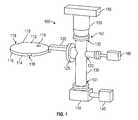
- FIGS. 1 through 6show one or more embodiments of a cooling chamber 200 or a cooler assembly 100 .
- FIG. 1shows a perspective view of a cooling assembly 100 in accordance with one or more embodiment of the disclosure.
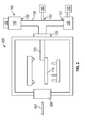
- FIG. 2shows a schematic representation of a cooling chamber 200 using the cooler assembly 100 .
- FIG. 2is an abbreviated view showing minimal components to illustrate the general configuration of the chamber 200 . Additional views of the individual components are found throughout the drawings.
- the cooler assembly 100includes a support plate 110 with a top surface 112 , a bottom surface 114 and sides 116 .
- the sides of the support plate 110can include one or more openings 118 on the sides 116 .
- the openings 118can be sized to fit around other components which may be used with or adjacent to the cooler assembly 100 .
- the support plate 110can be any suitable shape and size depending on, for example, the size and shape of a wafer to be cooled using the cooler assembly 100 .
- the support plate 110is generally disc shaped having a thickness and an average diameter.
- a generally disc shaped support plate 110can have one or more openings 118 or passages 119 formed through the thickness.
- the support plate 110is connected to a support arm 120 .
- the support arm 120can be movable or stationary.
- the support arm 120is configured to move in the z-axis to move the support plate 110 vertically.
- the support arm 120can be connected to a flange 125 which can be connected to the outer surface of a processing chamber 200 , as shown in FIG. 2 .
- the flange 125allows the support plate 110 and support arm 120 to be positioned within a process chamber while the remaining components of the cooler assembly 100 are outside of the processing chamber 200 .
- the flange 125can be connected to a housing 130 which can allow other components to be connected to the support plate 110 through the support arm 120 .
- a cryo pump 140is connected to the bottom end 131 of the housing 130 . While the embodiment shown has a vertically oriented housing 130 , those skilled in the art will understand that this is merely representative of one possible configuration and that other shapes and orientations are within the scope of the disclosure.
- a cry pump controller 145is connected to the cryo pump 140 to control the operation of the cryo pump 140 .
- the cryo pump 140can be any suitable cryo pump including, but not limited to, sorption pumps and cryo pumps that utilize liquid or compressed helium, dry ice, liquid nitrogen or have built-in cryocoolers. Condensation can be collected in the bottom of the cryopump and removed by tubing to allow the water to flow to waste, or by a flow of dry gas across the condensation collection area.
- the cryo pump 140can cool the wafer temperature to less than about 100 K. In some embodiments, the cryo pump 140 can maintain a temperature in the range of about 100 K to about 373 K. In some embodiments, the cryo pump 140 can cool the wafer to a temperature less than about room temperature, 250 K, 200 K, 150 K or 100 K.
- a turbo pump 150is connected to the top end 132 of the housing 130 .
- a turbo pump controller 155is connected to the turbo pump 150 to control the operation of the turbo pump 150 .
- the turbo pump 150can be any suitable turbomolecular pump capable of reaching a predetermined pressure range.
- the turbo pump 150is integrated into the housing 130 at junction 157 to prevent leakage of gases into the processing chamber.
- the cooling chamber 200includes a clamp ring 210 .
- the clamp ring 210has a top 212 and bottom 212 defining a thickness.
- the clamp ring 210has an inner diameter edge 213 and outer diameter edge 214 .
- the clamp ring 210includes one or more notched areas 215 which can be used to provide clearance for other components in the cooling chamber 200 .
- the notched area 215 in the embodiments shown in FIG. 4can fit around the support arm 120 when the components are in close proximity.
- the clamp ring 210includes a plurality of clamp pads 220 positioned against the bottom 212 and distributed around the inner diameter edge 213 .
- the clamp pad 220has a beveled surface 222 directed downward and toward the inner diameter edge 213 of the clamp ring 210 .
- the clamp pad 220can be any suitable shape and size. In some embodiments, the clamp pad 220 is generally round with a disc-like shape including the beveled surface 222 .
- the number of clamp pads 222can vary depending on, for example, the size of the clamp pads 222 , the size of the clamp ring 210 , the size of the wafer or the size of the cooling chamber 200 . In some embodiments, there are at least three clamp pads 222 . In some embodiments, there are in the range of 3 to 24 clamp pads 222 , or in the range of 3 to 18 clamp pads 222 , or in the range of 3 to 12 clamp pads 222 , or in the range of 4 to 10 clamp pads 222 , or in the range of 5 to 8 clamp pads, or 6 clamp pads.
- the inner edge 223 of the clamp pads 220can extend beyond the inner diameter edge 213 of the clamp ring 210 . In some embodiments, the clamp pads 220 do not extend beyond the inner diameter edge 213 of the clamp ring 210 .
- the clamp pads 220can be made from any suitable material including, but not limited to, quartz or thermally insulating materials. In some embodiments, the clamp pads 220 are made of quartz.
- the clamp pads 220can be connected to the clamp ring 210 by a permanent connection or by a releasable connection. In the embodiments shown, the clamp pads 220 are connected to the clamp ring 210 by one or more clamp bolts 224 .
- the clamp bolts 224can be positioned within recessed holes 226 in the clamp pads 220 so that the head of the clamp bolts 224 are not exposed. Recessing the clamp bolts 224 can prevent or minimize any contact damage that might occurs if the clamp ring 210 were to contact the wafer.
- the clamp pads 222can be connected directly to the bottom 212 of the clamp ring 210 .
- the clamp pads 222are positioned within recesses 229 formed in the bottom 212 of the clamp ring 210 .
- the recesses 229can be oversized or can fit the clamp pads snugly.
- the recesses 229are sized to provide an interference fit around the clamp pads 220 so that the clamp pads are held in place without additional hardware.
- FIGS. 5 and 6shows the clamp pads 220 and clamp ring 210 in use clamping a wafer 60 to the support plate 110 .
- FIG. 5shows a partial expanded view of the edge of the wafer 60 with the clamp pad 220 in contact.
- FIG. 6shows a further expanded view of region 6 of FIG. 5 .
- the clamp ring 210has been lowered, or the wafer 60 has been raised, so that the beveled surface 222 of the clamp pad 220 is in contact with an edge exclusion region 62 of the wafer 60 .
- the edge exclusion region 62(also referred to as an edge exclusion zone) of the wafer 60 is a region around the outer peripheral edge of the wafer 60 that no devices are formed on.
- the edge exclusion region 62provides an area on the wafer 60 that can be contacted without damaging the devices being formed thereon.
- the beveled surface 222 of the clamp pad 220allows for a minimal amount of contact at the edge exclusion zone.
- the beveled surface 222also allows for downward pressure to be applied only to the edge exclusion region 62 of the wafer 60 to hold the wafer to the support plate 110 .
- some embodimentsinclude a lift plate 240 to move the wafer 60 from a clamp position (as shown in FIG. 5 ) to a loading position (as shown in FIG. 9A ).
- the lift plate 240 of some embodimentsincludes a plurality of lift pins 242 . While FIG. 3 shows only one lift pin 242 , those skilled in the art will understand that more than one lift pin 242 can be included. For example, in some embodiments, there are at least three lift pins 242 .
- the lift pins 242have a top 243 that is suitable for contact with a wafer.
- the top 243 of the lift pin 242can be quartz, or a low friction material to prevent sliding of the wafer on the lift pins 240 .
- the lift plate 240is connected to the clamp ring 210 so that the lift plate 240 moves the clamp ring 210 and the wafer 60 .
- the support plate 110can include opening 118 to allow the lift pin 242 on the lift plate 240 to pass through the opening 118 .
- the lift plate 240is connected to a motor 247 to move the lift plate 240 between a loading position and a processing position.
- the motor 247can be any suitable type of motor that can move the lift plate 240 in the z-axis.
- the lift plate 240includes one or more openings 246 that may be located and sized to allow the lift plate 240 to move near other components without contacting the components.
- the opening 246may be sizes to allow the lift plate 240 to move adjacent the support arm 120 .
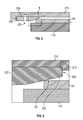
- some embodiments of the support plate 110include at least one channel 117 formed in the top surface 112 .
- the channel 117allows for a flow of gas against the back side of the wafer during cooling.
- the backside gas flowcan be used to increase the heat transfer between the wafer and the support plate 110 .
- the channel 117 shown in the Figureis a single spiral.
- the shape and number of channels 117can vary depending on, for example, the size of the support plate 110 and the heat transfer properties of the gas.
- the channel 117 formed in the top surface 112allows a flow of gas to pass beneath a wafer positioned on the top surface 112 .
- the support plate 110 of some embodimentsfurther comprises a backside gas line 127 connected to the back surface 114 of the support plate 110 and in fluid communication with the at least one channel 117 .
- the backside gas line 127connects to the support plate 110 at junction 270 .
- the junction 270can be a simple flange style connection that bolts the backside gas line 127 in place.
- the backside gas line 127can be connected to and in fluid communication with a gas source.
- the gas sourcecomprises argon.
- the backside gas linecan be maintained at a fixed pressure range.
- the gas entering the chamber 200 through the backside gas line 127can be removed from the chamber 200 using the turbo pump 150 .
- the pressure in the backside gas line 127 and the channel 117is in the range of about 1 Torr to about 10 Torr.
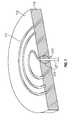
- the backside gas line 127is connected to the support plate 110 through a thermal choke 275 .
- the thermal choke 275can be any suitable connection that limits the thermal conductivity between the support plate 110 and the backside gas line 127 .
- FIG. 7shows a ball shaped thermal choke 275 which provides better regulation of the temperature of the support plate 110 by preventing thermal differences in the backside gas line 127 from changing the temperature of the support plate 110 .
- the thermal choke 275is made of a thermally insulating material.
- the thermal choke 275is made of quartz.
- the cluster tool 300includes at least one central transfer station with a plurality of sides.
- a robotis positioned within the central transfer station and is configured to move a robot blade to each of the plurality of sides.
- FIG. 8shows a schematic diagram of an illustrative multiple chamber semiconductor processing tool, also referred to as a cluster tool or multi-cluster tool.
- the cluster tool 800comprises a plurality of processing chambers 302 , 304 , 306 , 308 , 310 , 312 , 314 , 316 , 318 .
- the various processing chamberscan be any suitable chamber including, but not limited to, a preclean chamber, a buffer chamber, transfer space(s), a wafer orienter/degas chamber, a cryo cooling chamber, and a transfer chamber.
- the particular arrangement of process chambers and componentscan be varied depending on the cluster tool and should not be taken as limiting the scope of the disclosure.
- a factory interface 350is connected to a front of the cluster tool 300 .
- the factory interface 350includes a loading chamber 354 and an unloading chamber 356 on a front 351 of the factory interface 350 . While the loading chamber 354 is shown on the left and the unloading chamber 356 is shown on the right, those skilled in the art will understand that this is merely representative of one possible configuration.
- the size and shape of the loading chamber 354 and unloading chamber 356can vary depending on, for example, the substrates being processed in the cluster tool 300 .
- the loading chamber 354 and unloading chamber 356are sized to hold a wafer cassette with a plurality of wafers positioned within the cassette.
- a robot 352is within the factory interface 350 and can move between the loading chamber 354 and the unloading chamber 356 .
- the robot 352is capable of transferring a wafer from a cassette in the loading chamber 354 through the factory interface 350 to load lock chamber 360 .
- the robot 352is also capable of transferring a wafer from the load lock chamber 362 through the factory interface 350 to a cassette in the unloading chamber 356 .
- the factory interface 350can have more than one robot 352 .
- the factory interface 350may have a first robot that transfers wafers between the loading chamber 354 and load lock chamber 360 , and a second robot that transfers wafers between the load lock 362 and the unloading chamber 356 .
- the cluster tool 300 shownhas a first section 320 and a second section 330 .
- the first section 320is connected to the factory interface 350 through load lock chambers 360 , 362 .
- the first section 320includes a first transfer chamber 321 with at least one robot 325 positioned therein.
- the robot 325is also referred to as a robotic wafer transport mechanism.
- the first transfer chamber 321is centrally located with respect to the load lock chambers 360 , 362 , process chambers 302 , 304 , 316 , 318 and buffer chambers 322 , 324 .
- the robot 325 of some embodimentsis a multi-arm robot capable of independently moving more than one wafer at a time.
- the first transfer chamber 321comprises more than one robotic wafer transfer mechanism.
- the robot 325 in first transfer chamber 321is configured to move wafers between the chambers around the first transfer chamber 321 . Individual wafers are carried upon a wafer transport blade that is located at a distal end of
- the waferAfter processing a wafer in the first section 320 , the wafer can be passed to the second section 330 through a pass-through chamber.
- chambers 322 , 324can be uni-directional or bi-directional pass-through chambers.
- the pass-through chambers 322 , 324can be used, for example, to cryo cool the wafer before processing in the second section 330 , or allow wafer cooling or post-processing before moving back to the first section 320 .
- a cooling chamber 200is connected to a side of the central transfer station 321 , 331 .
- the cooling chamber 200includes a support plate connected to a cryo pump and turbo pump.
- the cryo pump and turbo pumpcan be located outside of the cooling chamber 200 to allow access to the units from outside the cluster tool.
- the cooling chamber 200is incorporated into the cluster tool 300 in either chamber 322 , 324 and can act as a pass-through.
- the cluster tool 300comprises a body 303 with a first section 320 and a second section 330 .
- the first section 320includes a first central transfer chamber 321 and a first plurality of processing chambers 302 , 304 , 316 , 318 .
- Each of the first plurality of processing chambersis connected to the first central transfer chamber 321 and is accessible by a first robot 325 located in the first central transfer chamber 321 .
- the second section 330includes a second central transfer chamber 331 and a second plurality of processing chambers 306 , 308 , 310 , 312 , 314 .
- Each of the second plurality of processing chambersis connected to the second central transfer chamber 331 and is accessible by a second robot 335 located in the second central transfer chamber 331 .
- a system controller 390is in communication with the first robot 325 , second robot 335 , first plurality of processing chambers 302 , 304 , 316 , 318 and second plurality of processing chambers 306 , 308 , 310 , 312 , 314 .
- the system controller 390can be any suitable component that can control the processing chambers and robots.
- the system controller 390can be a computer including a central processing unit, memory, suitable circuits and storage.
- incorporating a cooling chamber 200 into the cluster tool 300allows for a decrease in pressure of the overall cluster tool 300 .
- a cluster tool 300is typically able to maintain a pressure of about 10 ⁇ 8 Torr.
- the inventorshave found that incorporating the cooling chamber 200 decreased the pressure to the low-mid 10 ⁇ 9 Torr range.
- a pressure in the central transfer station 321 , 331is decreased by greater than about 1 ⁇ 2 order of magnitude or 1 order of magnitude when the cooling chamber is set to a temperature less than about 150 K.
- FIG. 9Ashows an embodiment of the cooling chamber in the loading position where the wafer 60 is supported by the lift pins 242 so that there is a space 295 between the wafer 60 and the support plate 110 .
- the space 295 in the loading/unloading positionis large enough to allow a robot blade 297 to pass through slit valve 298 into the chamber 200 to move the wafer 60 in or out of the chamber 200 .
- the wafer 60is positioned in the cooling chamber 200 and cooled to a predetermined temperature.
- the clamp ring 210 and clamp pads 220are above the wafer 60 and the support plate 110 is below the lift pins 242 .
- the wafer 60is positioned on a plurality of lift pins 242 connected to the lift plate 240 .
- the plurality of lift pins 242are elevated above the top surface 112 of the support plate 110 .
- the lift plate 240is lowered so that the lift pins 242 lower the wafer 60 to contact the top surface 112 of the support plate 110 . While lowering the lift pins 242 , as shown in FIG. 9B , the lift pins 242 pass through openings 118 and the opening 246 in the lift plate 240 move past the support arm 120 .
- the lift plate 240has been lowered to the point where the wafer 60 is resting on the support plate 110 and the lift pins 242 are beginning to move below the wafer 60 .
- lowering the lift plate 240causes the lift pins 242 and the clamp ring 210 to be lowered.
- the clamp ring 210is connected to the lift plate 240 so that the movements are coordinated.
- the clamp ring 210is lowered so that the beveled surface of the clamp pads 220 contact the outer peripheral edge of the wafer 60 in the edge exclusion zone.
- the contact of the clamp pads 220 with the wafer 60clamp the wafer 60 to the support plate 110 .
- the wafer 60can be removed from the chamber 200 .
- Removing the wafer 60 from the cooling chamber 200is basically a reverse of the loading process.
- the clamp ring 210is lifted so that the clamp pads 220 are no longer contacting the wafer 60 .
- the lift pins 242are lifted to contact the wafer 60 and elevate the wafer 60 above the top surface 112 of the support plate 110 so that there is a space 295 below the wafer 60 sufficient to allow a robot blade 297 to move between the wafer 60 and the support plate 110 .
- the lift plate 240elevates the lift pins 242 so that a top of the lift pins 242 are above the top surface 112 of the support plate 110 by a distance sufficient to allow a robot 297 blade to pass between the top of the lift pins 242 and the top surface 112 of the support plate 110 .
- kits for providing a cooling chamber in an existing cluster toolincludes the cooling assembly 100 shown in FIG. 1 .
- the kitincludes an outer plate for the cluster tool to allow for the positioning of the cooling assembly 100 to allow the cryo pump 140 and turbo pump 150 to remain outside of the cluster tool.
Landscapes
- Engineering & Computer Science (AREA)
- Chemical & Material Sciences (AREA)
- Computer Hardware Design (AREA)
- Condensed Matter Physics & Semiconductors (AREA)
- Power Engineering (AREA)
- Microelectronics & Electronic Packaging (AREA)
- Manufacturing & Machinery (AREA)
- General Physics & Mathematics (AREA)
- Physics & Mathematics (AREA)
- Metallurgy (AREA)
- Organic Chemistry (AREA)
- Chemical Kinetics & Catalysis (AREA)
- General Chemical & Material Sciences (AREA)
- Mechanical Engineering (AREA)
- Materials Engineering (AREA)
- Container, Conveyance, Adherence, Positioning, Of Wafer (AREA)
Abstract
Description
- This application claims priority to U.S. Provisional Application No. 62/433,194, filed Dec. 12, 2016, the entire disclosure of which is hereby incorporated by reference herein.
- The present disclosure relates generally to apparatus to rapidly cool semiconductor wafers to cryogenic temperatures and methods of use. In particular, embodiments of the disclosure are directed to apparatus to rapidly cool semiconductor wafers as stand-alone systems or incorporated into cluster tools.
- Semiconductor device formation is commonly conducted in substrate processing systems or platforms containing multiple chambers, which may also be referred to as cluster tools. In some instances, the purpose of a multi-chamber processing platform or cluster tool is to perform two or more processes on a substrate sequentially in a controlled environment. In other instances, however, a multiple chamber processing platform may only perform a single processing step on substrates. The additional chambers can be employed to maximize the rate at which substrates are processed. In the latter case, the process performed on substrates is typically a batch process, wherein a relatively large number of substrates, e.g. 25 or 50, are processed in a given chamber simultaneously. Batch processing is especially beneficial for processes that are too time-consuming to be performed on individual substrates in an economically viable manner, such as for atomic layer deposition (ALD) processes and some chemical vapor deposition (CVD) processes.
- During processing, many parameters are controlled including the temperature of the wafer. In some processes, decreasing the temperature of a semiconductor wafer during processing can change film properties. However, cooling the wafer temperature can be a time-consuming process that can affect the overall throughput of a process performed in a batch processing chamber.
- Therefore, there is a need in the art for apparatus and methods to rapidly cool the temperature of a semiconductor wafer without significantly affecting the overall system throughput.
- One or more embodiments of the disclosure are directed to cooling chambers comprising a support plate connected to a cryo pump and a turbo pump. The support plate has a top surface to support a wafer. The cooling chamber includes a clamp ring having a top, bottom, inner diameter, outer diameter and a plurality of clamp pads on the bottom. Each clamp pad has a beveled surface directed downward and toward the inner diameter. A lift plate is included to move the clamp ring from a clamp position to a loading position.
- Additional embodiments of the disclosure are directed to cluster tools comprising a central transfer station with a plurality of sides, a robot and a cooling chamber. The robot is positioned within the central transfer station and is configured to move a robot blade to each of the plurality of sides. The cooling chamber is connected to a side of the central transfer station. The cooling chamber includes a support plate connected to a cryo pump and turbo pump. The support plate has a top surface to support a wafer. A clamp ring having a top, bottom, inner diameter, outer diameter and a plurality of clamp pads on the bottom is included. Each clamp pad has a beveled surface directed downward and toward the inner diameter. A lift plate is included to move the clamp ring from a clamp position to a loading position.
- Further embodiments of the disclosure are directed to methods of cooling a wafer. A wafer is positioned in a cooling chamber comprising a support plate connected to a cryo pump and turbo pump. The support plate has a top surface to support a wafer. A clamp ring has a top, bottom, inner diameter, outer diameter and a plurality of clamp pads on the bottom. Each clamp pad has a beveled surface directed downward and toward the inner diameter. A lift plate moves the clamp ring from a clamp position to a loading position. The wafer is cooled to a temperature less than about 150 K using the cryo pump.
- So that the manner in which the above recited features of the present disclosure can be understood in detail, a more particular description of the disclosure, briefly summarized above, may be had by reference to embodiments, some of which are illustrated in the appended drawings. It is to be noted, however, that the appended drawings illustrate only typical embodiments of this disclosure and are therefore not to be considered limiting of its scope, for the disclosure may admit to other equally effective embodiments.
FIG. 1 shows a view of a cooling assembly in accordance with one or more embodiment of the disclosure;FIG. 2 shows a cross-sectional schematic view of a cooling chamber in accordance with one or more embodiment of the disclosure;FIG. 3 shows a cross-sectional perspective view of a cooling chamber in accordance with one or more embodiment of the disclosure;FIG. 4 shows a perspective view of a clamp ring in accordance with one or more embodiment of the disclosure;FIG. 5 shows a partial cross-sectional view of the cooling chamber in accordance with one or more embodiment of the disclosure;FIG. 6 shows an expanded view ofregion 6 fromFIG. 5 ;FIG. 7 shows a cross-sectional perspective view of support plate in accordance with one or more embodiment of the disclosure;FIG. 8 shows a schematic view of a cluster tool in accordance with one or more embodiment of the disclosure; andFIGS. 9A through 9C show a schematic representation of a method of cooling a wafer in accordance with one or more embodiment of the disclosure.- Before describing several exemplary embodiments of the disclosure, it is to be understood that the disclosure is not limited to the details of construction or process steps set forth in the following description. The disclosure is capable of other embodiments and of being practiced or being carried out in various ways.
- A “substrate” as used herein, refers to any substrate or material surface formed on a substrate upon which film processing is performed during a fabrication process. For example, a substrate surface on which processing can be performed include materials such as silicon, silicon oxide, strained silicon, silicon on insulator (SOI), carbon doped silicon oxides, amorphous silicon, doped silicon, germanium, gallium arsenide, glass, sapphire, and any other materials such as metals, metal nitrides, metal alloys, and other conductive materials, depending on the application. Substrates include, without limitation, semiconductor wafers. Substrates may be exposed to a pretreatment process to polish, etch, reduce, oxidize, hydroxylate, anneal and/or bake the substrate surface. In addition to film processing directly on the surface of the substrate itself, in the present disclosure, any of the film processing steps disclosed may also be performed on an under-layer formed on the substrate as disclosed in more detail below, and the term “substrate surface” is intended to include such under-layer as the context indicates. Thus for example, where a film/layer or partial film/layer has been deposited onto a substrate surface, the exposed surface of the newly deposited film/layer becomes the substrate surface.
- As used in this specification and the appended claims, the terms “precursor”, “reactant”, “reactive gas” and the like are used interchangeably to refer to any gaseous species that can react with the substrate surface.
- Embodiments of the disclosure provide a cryogenic cooling system that can be used as a stand-alone component or integrated into a batch processing system. An in-situ wafer cooling station can be used to pre-cool wafers to a temperature in the range of less than about 100 K to room temperature (˜293 K) to about 100° C. (373 K). Some embodiments of the disclosure advantageously provide cooling chambers that can be used to reduce film roughness and tunneling magneto-resistance in a deposited film.
- Some embodiments of the disclosure provide systems with higher vacuum levels (10−9Torr) than are currently reached (10−8Torr). The system can incorporate a mechanical clamping component with a back side gas flow to increase the effectiveness of heat transfer. In some embodiments, a wafer can be cooled from about room temperature to 110 K in less than 3 minutes.
- Some embodiments of the disclosure provide apparatus and methods to load and unload wafers from the cryogenic chamber using a robot blade and wafer clamp.
- Some embodiments of the disclosure provide gas conduction and choking which can be increased using a backside gas line with cooled gas to improve heat transfer between the cold plate and the wafer. The backside gas line can be evacuated using an integrated turbo pump or through a separate vacuum source. In some embodiments, a ball mechanism provides a thermal choke to prevent the stage from losing heat during use.
FIGS. 1 through 6 show one or more embodiments of acooling chamber 200 or acooler assembly 100.FIG. 1 shows a perspective view of acooling assembly 100 in accordance with one or more embodiment of the disclosure.FIG. 2 shows a schematic representation of acooling chamber 200 using thecooler assembly 100.FIG. 2 is an abbreviated view showing minimal components to illustrate the general configuration of thechamber 200. Additional views of the individual components are found throughout the drawings.- Referring to
FIG. 1 one or more embodiments of the disclosure are directed tocooler assemblies 100. Thecooler assembly 100 includes asupport plate 110 with atop surface 112, abottom surface 114 and sides116. The sides of thesupport plate 110 can include one ormore openings 118 on thesides 116. Theopenings 118 can be sized to fit around other components which may be used with or adjacent to thecooler assembly 100. - The
support plate 110 can be any suitable shape and size depending on, for example, the size and shape of a wafer to be cooled using thecooler assembly 100. In some embodiments, thesupport plate 110 is generally disc shaped having a thickness and an average diameter. A generally disc shapedsupport plate 110 can have one ormore openings 118 orpassages 119 formed through the thickness. - The
support plate 110 is connected to asupport arm 120. Thesupport arm 120 can be movable or stationary. In some embodiments, thesupport arm 120 is configured to move in the z-axis to move thesupport plate 110 vertically. - The
support arm 120 can be connected to aflange 125 which can be connected to the outer surface of aprocessing chamber 200, as shown inFIG. 2 . Theflange 125 allows thesupport plate 110 andsupport arm 120 to be positioned within a process chamber while the remaining components of thecooler assembly 100 are outside of theprocessing chamber 200. - The
flange 125 can be connected to ahousing 130 which can allow other components to be connected to thesupport plate 110 through thesupport arm 120. In the embodiments shown inFIGS. 1 and 2 , acryo pump 140 is connected to thebottom end 131 of thehousing 130. While the embodiment shown has a vertically orientedhousing 130, those skilled in the art will understand that this is merely representative of one possible configuration and that other shapes and orientations are within the scope of the disclosure. Acry pump controller 145 is connected to thecryo pump 140 to control the operation of thecryo pump 140. The cryo pump140 can be any suitable cryo pump including, but not limited to, sorption pumps and cryo pumps that utilize liquid or compressed helium, dry ice, liquid nitrogen or have built-in cryocoolers. Condensation can be collected in the bottom of the cryopump and removed by tubing to allow the water to flow to waste, or by a flow of dry gas across the condensation collection area. - The cryo pump140 can cool the wafer temperature to less than about 100 K. In some embodiments, the
cryo pump 140 can maintain a temperature in the range of about 100 K to about 373 K. In some embodiments, thecryo pump 140 can cool the wafer to a temperature less than about room temperature, 250 K, 200 K, 150 K or 100 K. - In the embodiment shown, a
turbo pump 150 is connected to thetop end 132 of thehousing 130. Aturbo pump controller 155 is connected to theturbo pump 150 to control the operation of theturbo pump 150. Theturbo pump 150 can be any suitable turbomolecular pump capable of reaching a predetermined pressure range. In some embodiments, theturbo pump 150 is integrated into thehousing 130 atjunction 157 to prevent leakage of gases into the processing chamber. - Referring to
FIGS. 3 through 6 , the coolingchamber 200 includes aclamp ring 210. Theclamp ring 210 has a top212 and bottom212 defining a thickness. Theclamp ring 210 has aninner diameter edge 213 andouter diameter edge 214. In some embodiments, theclamp ring 210 includes one or more notchedareas 215 which can be used to provide clearance for other components in thecooling chamber 200. For example, the notchedarea 215 in the embodiments shown inFIG. 4 can fit around thesupport arm 120 when the components are in close proximity. - The
clamp ring 210 includes a plurality ofclamp pads 220 positioned against the bottom212 and distributed around theinner diameter edge 213. Theclamp pad 220 has abeveled surface 222 directed downward and toward theinner diameter edge 213 of theclamp ring 210. Theclamp pad 220 can be any suitable shape and size. In some embodiments, theclamp pad 220 is generally round with a disc-like shape including thebeveled surface 222. - The number of
clamp pads 222 can vary depending on, for example, the size of theclamp pads 222, the size of theclamp ring 210, the size of the wafer or the size of thecooling chamber 200. In some embodiments, there are at least threeclamp pads 222. In some embodiments, there are in the range of 3 to 24clamp pads 222, or in the range of 3 to 18clamp pads 222, or in the range of 3 to 12clamp pads 222, or in the range of 4 to 10clamp pads 222, or in the range of 5 to 8 clamp pads, or 6 clamp pads. - The
inner edge 223 of theclamp pads 220 can extend beyond theinner diameter edge 213 of theclamp ring 210. In some embodiments, theclamp pads 220 do not extend beyond theinner diameter edge 213 of theclamp ring 210. - The
clamp pads 220 can be made from any suitable material including, but not limited to, quartz or thermally insulating materials. In some embodiments, theclamp pads 220 are made of quartz. - The
clamp pads 220 can be connected to theclamp ring 210 by a permanent connection or by a releasable connection. In the embodiments shown, theclamp pads 220 are connected to theclamp ring 210 by one ormore clamp bolts 224. Theclamp bolts 224 can be positioned within recessedholes 226 in theclamp pads 220 so that the head of theclamp bolts 224 are not exposed. Recessing theclamp bolts 224 can prevent or minimize any contact damage that might occurs if theclamp ring 210 were to contact the wafer. - The
clamp pads 222 can be connected directly to thebottom 212 of theclamp ring 210. In some embodiments, theclamp pads 222 are positioned withinrecesses 229 formed in thebottom 212 of theclamp ring 210. Therecesses 229 can be oversized or can fit the clamp pads snugly. In some embodiments, therecesses 229 are sized to provide an interference fit around theclamp pads 220 so that the clamp pads are held in place without additional hardware. FIGS. 5 and 6 shows theclamp pads 220 andclamp ring 210 in use clamping awafer 60 to thesupport plate 110.FIG. 5 shows a partial expanded view of the edge of thewafer 60 with theclamp pad 220 in contact.FIG. 6 shows a further expanded view ofregion 6 ofFIG. 5 . In the embodiment shown, theclamp ring 210 has been lowered, or thewafer 60 has been raised, so that thebeveled surface 222 of theclamp pad 220 is in contact with anedge exclusion region 62 of thewafer 60. The edge exclusion region62 (also referred to as an edge exclusion zone) of thewafer 60 is a region around the outer peripheral edge of thewafer 60 that no devices are formed on. Theedge exclusion region 62 provides an area on thewafer 60 that can be contacted without damaging the devices being formed thereon.- The
beveled surface 222 of theclamp pad 220 allows for a minimal amount of contact at the edge exclusion zone. Thebeveled surface 222 also allows for downward pressure to be applied only to theedge exclusion region 62 of thewafer 60 to hold the wafer to thesupport plate 110. - Referring back to
FIG. 3 , some embodiments include alift plate 240 to move thewafer 60 from a clamp position (as shown inFIG. 5 ) to a loading position (as shown inFIG. 9A ). - The
lift plate 240 of some embodiments includes a plurality of lift pins242. WhileFIG. 3 shows only onelift pin 242, those skilled in the art will understand that more than onelift pin 242 can be included. For example, in some embodiments, there are at least three lift pins242. The lift pins242 have a top243 that is suitable for contact with a wafer. For example, the top243 of thelift pin 242 can be quartz, or a low friction material to prevent sliding of the wafer on the lift pins240. - In some embodiments, the
lift plate 240 is connected to theclamp ring 210 so that thelift plate 240 moves theclamp ring 210 and thewafer 60. Thesupport plate 110 can include opening118 to allow thelift pin 242 on thelift plate 240 to pass through theopening 118. - In some embodiments, the
lift plate 240 is connected to amotor 247 to move thelift plate 240 between a loading position and a processing position. Themotor 247 can be any suitable type of motor that can move thelift plate 240 in the z-axis. - In some embodiments, the
lift plate 240 includes one ormore openings 246 that may be located and sized to allow thelift plate 240 to move near other components without contacting the components. For example, as described with respect toFIG. 9A , theopening 246 may be sizes to allow thelift plate 240 to move adjacent thesupport arm 120. - Referring to
FIG. 7 , some embodiments of thesupport plate 110 include at least onechannel 117 formed in thetop surface 112. Thechannel 117 allows for a flow of gas against the back side of the wafer during cooling. The backside gas flow can be used to increase the heat transfer between the wafer and thesupport plate 110. While the view shows a cross-section of thesupport plate 110, thechannel 117 shown in the Figure is a single spiral. The shape and number ofchannels 117 can vary depending on, for example, the size of thesupport plate 110 and the heat transfer properties of the gas. Thechannel 117 formed in thetop surface 112 allows a flow of gas to pass beneath a wafer positioned on thetop surface 112. - The
support plate 110 of some embodiments further comprises abackside gas line 127 connected to theback surface 114 of thesupport plate 110 and in fluid communication with the at least onechannel 117. Thebackside gas line 127 connects to thesupport plate 110 atjunction 270. Thejunction 270 can be a simple flange style connection that bolts thebackside gas line 127 in place. - The
backside gas line 127 can be connected to and in fluid communication with a gas source. In some embodiments, the gas source comprises argon. The backside gas line can be maintained at a fixed pressure range. The gas entering thechamber 200 through thebackside gas line 127 can be removed from thechamber 200 using theturbo pump 150. In some embodiments, the pressure in thebackside gas line 127 and thechannel 117 is in the range of about 1 Torr to about 10 Torr. - In some embodiments, the
backside gas line 127 is connected to thesupport plate 110 through athermal choke 275. Thethermal choke 275 can be any suitable connection that limits the thermal conductivity between thesupport plate 110 and thebackside gas line 127. For example,FIG. 7 shows a ball shapedthermal choke 275 which provides better regulation of the temperature of thesupport plate 110 by preventing thermal differences in thebackside gas line 127 from changing the temperature of thesupport plate 110. In some embodiments, thethermal choke 275 is made of a thermally insulating material. In some embodiments, thethermal choke 275 is made of quartz. - Some embodiments of the disclosure are directed to cluster
tools 300, as shown inFIG. 8 . Thecluster tool 300 includes at least one central transfer station with a plurality of sides. A robot is positioned within the central transfer station and is configured to move a robot blade to each of the plurality of sides. FIG. 8 shows a schematic diagram of an illustrative multiple chamber semiconductor processing tool, also referred to as a cluster tool or multi-cluster tool. The cluster tool800 comprises a plurality ofprocessing chambers - In the embodiment shown in
FIG. 8 , afactory interface 350 is connected to a front of thecluster tool 300. Thefactory interface 350 includes aloading chamber 354 and anunloading chamber 356 on a front351 of thefactory interface 350. While theloading chamber 354 is shown on the left and theunloading chamber 356 is shown on the right, those skilled in the art will understand that this is merely representative of one possible configuration. - The size and shape of the
loading chamber 354 and unloadingchamber 356 can vary depending on, for example, the substrates being processed in thecluster tool 300. In the embodiment shown, theloading chamber 354 and unloadingchamber 356 are sized to hold a wafer cassette with a plurality of wafers positioned within the cassette. - A
robot 352 is within thefactory interface 350 and can move between theloading chamber 354 and theunloading chamber 356. Therobot 352 is capable of transferring a wafer from a cassette in theloading chamber 354 through thefactory interface 350 to loadlock chamber 360. Therobot 352 is also capable of transferring a wafer from theload lock chamber 362 through thefactory interface 350 to a cassette in theunloading chamber 356. As will be understood by those skilled in the art, thefactory interface 350 can have more than onerobot 352. For example, thefactory interface 350 may have a first robot that transfers wafers between theloading chamber 354 and loadlock chamber 360, and a second robot that transfers wafers between theload lock 362 and theunloading chamber 356. - The
cluster tool 300 shown has afirst section 320 and asecond section 330. Thefirst section 320 is connected to thefactory interface 350 throughload lock chambers first section 320 includes afirst transfer chamber 321 with at least onerobot 325 positioned therein. Therobot 325 is also referred to as a robotic wafer transport mechanism. Thefirst transfer chamber 321 is centrally located with respect to theload lock chambers process chambers buffer chambers robot 325 of some embodiments is a multi-arm robot capable of independently moving more than one wafer at a time. In some embodiments, thefirst transfer chamber 321 comprises more than one robotic wafer transfer mechanism. Therobot 325 infirst transfer chamber 321 is configured to move wafers between the chambers around thefirst transfer chamber 321. Individual wafers are carried upon a wafer transport blade that is located at a distal end of the first robotic mechanism. - After processing a wafer in the
first section 320, the wafer can be passed to thesecond section 330 through a pass-through chamber. For example,chambers chambers second section 330, or allow wafer cooling or post-processing before moving back to thefirst section 320. - In some embodiments, a
cooling chamber 200 is connected to a side of thecentral transfer station chamber 200 includes a support plate connected to a cryo pump and turbo pump. The cryo pump and turbo pump can be located outside of thecooling chamber 200 to allow access to the units from outside the cluster tool. In some embodiments, the coolingchamber 200 is incorporated into thecluster tool 300 in eitherchamber - One or more embodiments of the disclosure are directed to cluster
tools 300. Thecluster tool 300 comprises abody 303 with afirst section 320 and asecond section 330. Thefirst section 320 includes a firstcentral transfer chamber 321 and a first plurality ofprocessing chambers central transfer chamber 321 and is accessible by afirst robot 325 located in the firstcentral transfer chamber 321. Thesecond section 330 includes a secondcentral transfer chamber 331 and a second plurality ofprocessing chambers central transfer chamber 331 and is accessible by asecond robot 335 located in the secondcentral transfer chamber 331. - A
system controller 390 is in communication with thefirst robot 325,second robot 335, first plurality ofprocessing chambers processing chambers system controller 390 can be any suitable component that can control the processing chambers and robots. For example, thesystem controller 390 can be a computer including a central processing unit, memory, suitable circuits and storage. - It has been surprisingly found that incorporating a
cooling chamber 200 into thecluster tool 300 allows for a decrease in pressure of theoverall cluster tool 300. For example, acluster tool 300 is typically able to maintain a pressure of about 10−8Torr. The inventors have found that incorporating thecooling chamber 200 decreased the pressure to the low-mid 10−9Torr range. In some embodiments, a pressure in thecentral transfer station - With reference to
FIGS. 2 and 9A through 9C , some embodiments of the disclosure are directed to methods of cooling awafer 60.FIG. 9A shows an embodiment of the cooling chamber in the loading position where thewafer 60 is supported by the lift pins242 so that there is aspace 295 between thewafer 60 and thesupport plate 110. Thespace 295 in the loading/unloading position is large enough to allow arobot blade 297 to pass throughslit valve 298 into thechamber 200 to move thewafer 60 in or out of thechamber 200. - The
wafer 60 is positioned in thecooling chamber 200 and cooled to a predetermined temperature. InFIG. 9A , theclamp ring 210 and clamppads 220 are above thewafer 60 and thesupport plate 110 is below the lift pins242. - The
wafer 60 is positioned on a plurality of lift pins242 connected to thelift plate 240. The plurality of lift pins242 are elevated above thetop surface 112 of thesupport plate 110. - The
lift plate 240 is lowered so that the lift pins242 lower thewafer 60 to contact thetop surface 112 of thesupport plate 110. While lowering the lift pins242, as shown inFIG. 9B , the lift pins242 pass throughopenings 118 and theopening 246 in thelift plate 240 move past thesupport arm 120. - In
FIG. 9B , thelift plate 240 has been lowered to the point where thewafer 60 is resting on thesupport plate 110 and the lift pins242 are beginning to move below thewafer 60. In some embodiments, lowering thelift plate 240 causes the lift pins242 and theclamp ring 210 to be lowered. In some embodiments, theclamp ring 210 is connected to thelift plate 240 so that the movements are coordinated. - In
FIG. 9C , theclamp ring 210 is lowered so that the beveled surface of theclamp pads 220 contact the outer peripheral edge of thewafer 60 in the edge exclusion zone. The contact of theclamp pads 220 with thewafer 60 clamp thewafer 60 to thesupport plate 110. - After the wafer has been cooled to the predetermined temperature, the
wafer 60 can be removed from thechamber 200. Removing thewafer 60 from the coolingchamber 200 is basically a reverse of the loading process. Theclamp ring 210 is lifted so that theclamp pads 220 are no longer contacting thewafer 60. - The lift pins242 are lifted to contact the
wafer 60 and elevate thewafer 60 above thetop surface 112 of thesupport plate 110 so that there is aspace 295 below thewafer 60 sufficient to allow arobot blade 297 to move between thewafer 60 and thesupport plate 110. In some embodiments, when in the loading position, thelift plate 240 elevates the lift pins242 so that a top of the lift pins242 are above thetop surface 112 of thesupport plate 110 by a distance sufficient to allow arobot 297 blade to pass between the top of the lift pins242 and thetop surface 112 of thesupport plate 110. - Some embodiments of the disclosure are directed to kits for providing a cooling chamber in an existing cluster tool. The kit of some embodiments includes the cooling
assembly 100 shown inFIG. 1 . In some embodiments, the kit includes an outer plate for the cluster tool to allow for the positioning of the coolingassembly 100 to allow thecryo pump 140 andturbo pump 150 to remain outside of the cluster tool. - Reference throughout this specification to “one embodiment,” “certain embodiments,” “one or more embodiments” or “an embodiment” means that a particular feature, structure, material, or characteristic described in connection with the embodiment is included in at least one embodiment of the disclosure. Thus, the appearances of the phrases such as “in one or more embodiments,” “in certain embodiments,” “in one embodiment” or “in an embodiment” in various places throughout this specification are not necessarily referring to the same embodiment of the disclosure. Furthermore, the particular features, structures, materials, or characteristics may be combined in any suitable manner in one or more embodiments.
- Although the disclosure herein has been described with reference to particular embodiments, it is to be understood that these embodiments are merely illustrative of the principles and applications of the present disclosure. It will be apparent to those skilled in the art that various modifications and variations can be made to the method and apparatus of the present disclosure without departing from the spirit and scope of the disclosure. Thus, it is intended that the present disclosure include modifications and variations that are within the scope of the appended claims and their equivalents.
Claims (20)
Priority Applications (1)
| Application Number | Priority Date | Filing Date | Title |
|---|---|---|---|
| US15/839,018US11802340B2 (en) | 2016-12-12 | 2017-12-12 | UHV in-situ cryo-cool chamber |
Applications Claiming Priority (2)
| Application Number | Priority Date | Filing Date | Title |
|---|---|---|---|
| US201662433194P | 2016-12-12 | 2016-12-12 | |
| US15/839,018US11802340B2 (en) | 2016-12-12 | 2017-12-12 | UHV in-situ cryo-cool chamber |
Publications (2)
| Publication Number | Publication Date |
|---|---|
| US20180163306A1true US20180163306A1 (en) | 2018-06-14 |
| US11802340B2 US11802340B2 (en) | 2023-10-31 |
Family
ID=62488512
Family Applications (1)
| Application Number | Title | Priority Date | Filing Date |
|---|---|---|---|
| US15/839,018Active2039-11-16US11802340B2 (en) | 2016-12-12 | 2017-12-12 | UHV in-situ cryo-cool chamber |
Country Status (1)
| Country | Link |
|---|---|
| US (1) | US11802340B2 (en) |
Cited By (3)
| Publication number | Priority date | Publication date | Assignee | Title |
|---|---|---|---|---|
| CN110326733A (en)* | 2019-07-15 | 2019-10-15 | 山东华春新能源有限公司 | A kind of super-pressure quick freezing equipment |
| US11393702B2 (en)* | 2019-07-01 | 2022-07-19 | Tokyo Electron Limited | Heat treatment apparatus and heat treatment method |
| US11430678B2 (en)* | 2018-07-17 | 2022-08-30 | Asml Netherlands B.V. | Particle beam inspection apparatus |
Citations (74)
| Publication number | Priority date | Publication date | Assignee | Title |
|---|---|---|---|---|
| US4086555A (en)* | 1976-05-27 | 1978-04-25 | General Dynamics Corporation | Photoconductive sensor |
| US4508161A (en)* | 1982-05-25 | 1985-04-02 | Varian Associates, Inc. | Method for gas-assisted, solid-to-solid thermal transfer with a semiconductor wafer |
| US4543059A (en)* | 1984-07-18 | 1985-09-24 | Quartz Engineering & Materials, Inc. | Slotted cantilever diffusion tube system and method and apparatus for loading |
| US4603466A (en)* | 1984-02-17 | 1986-08-05 | Gca Corporation | Wafer chuck |
| US4717461A (en)* | 1986-09-15 | 1988-01-05 | Machine Technology, Inc. | System and method for processing workpieces |
| US4842683A (en)* | 1986-12-19 | 1989-06-27 | Applied Materials, Inc. | Magnetic field-enhanced plasma etch reactor |
| US4892753A (en)* | 1986-12-19 | 1990-01-09 | Applied Materials, Inc. | Process for PECVD of silicon oxide using TEOS decomposition |
| US4909314A (en)* | 1979-12-21 | 1990-03-20 | Varian Associates, Inc. | Apparatus for thermal treatment of a wafer in an evacuated environment |
| US4911597A (en)* | 1985-01-22 | 1990-03-27 | Applied Materials, Inc. | Semiconductor processing system with robotic autoloader and load lock |
| US4915564A (en)* | 1986-04-04 | 1990-04-10 | Materials Research Corporation | Method and apparatus for handling and processing wafer-like materials |
| US4917556A (en)* | 1986-04-28 | 1990-04-17 | Varian Associates, Inc. | Modular wafer transport and processing system |
| US4923584A (en)* | 1988-10-31 | 1990-05-08 | Eaton Corporation | Sealing apparatus for a vacuum processing system |
| US4938691A (en)* | 1987-11-17 | 1990-07-03 | Tel Sagami Limited | Heat-treating apparatus |
| US4944860A (en)* | 1988-11-04 | 1990-07-31 | Eaton Corporation | Platen assembly for a vacuum processing system |
| US5019233A (en)* | 1988-10-31 | 1991-05-28 | Eaton Corporation | Sputtering system |
| US5094885A (en)* | 1990-10-12 | 1992-03-10 | Genus, Inc. | Differential pressure cvd chuck |
| US5154582A (en)* | 1991-08-20 | 1992-10-13 | Danielson Associates, Inc. | Rough vacuum pump using bulk getter material |
| US5215619A (en)* | 1986-12-19 | 1993-06-01 | Applied Materials, Inc. | Magnetic field-enhanced plasma etch reactor |
| US5224809A (en)* | 1985-01-22 | 1993-07-06 | Applied Materials, Inc. | Semiconductor processing system with robotic autoloader and load lock |
| US5280983A (en)* | 1985-01-22 | 1994-01-25 | Applied Materials, Inc. | Semiconductor processing system with robotic autoloader and load lock |
| US5292393A (en)* | 1986-12-19 | 1994-03-08 | Applied Materials, Inc. | Multichamber integrated process system |
| US5310410A (en)* | 1990-04-06 | 1994-05-10 | Sputtered Films, Inc. | Method for processing semi-conductor wafers in a multiple vacuum and non-vacuum chamber apparatus |
| US5437757A (en)* | 1994-01-21 | 1995-08-01 | Applied Materials, Inc. | Clamp ring for domed pedestal in wafer processing chamber |
| US5494523A (en)* | 1993-05-13 | 1996-02-27 | Applied Materials, Inc. | Controlling plasma particulates by contouring the plasma sheath using materials of differing RF impedances |
| US5513594A (en)* | 1993-10-20 | 1996-05-07 | Mcclanahan; Adolphus E. | Clamp with wafer release for semiconductor wafer processing equipment |
| US5685963A (en)* | 1994-10-31 | 1997-11-11 | Saes Pure Gas, Inc. | In situ getter pump system and method |
| US5725718A (en)* | 1992-10-27 | 1998-03-10 | Applied Materials, Inc. | Clamp ring for domed heated pedestal in wafer processing chamber |
| US5730801A (en)* | 1994-08-23 | 1998-03-24 | Applied Materials, Inc. | Compartnetalized substrate processing chamber |
| US5753133A (en)* | 1994-07-11 | 1998-05-19 | Applied Komatsu Technology, Inc. | Method and apparatus for etching film layers on large substrates |
| US5799860A (en)* | 1995-08-07 | 1998-09-01 | Applied Materials, Inc. | Preparation and bonding of workpieces to form sputtering targets and other assemblies |
| US5804042A (en)* | 1995-06-07 | 1998-09-08 | Tokyo Electron Limited | Wafer support structure for a wafer backplane with a curved surface |
| US5911834A (en)* | 1996-11-18 | 1999-06-15 | Applied Materials, Inc. | Gas delivery system |
| US5930661A (en)* | 1996-10-15 | 1999-07-27 | Vanguard International Semiconductor Corporation | Substrate clamp design for minimizing substrate to clamp sticking during thermal processing of thermally flowable layers |
| US5942041A (en)* | 1996-09-16 | 1999-08-24 | Mosel-Vitelic, Inc. | Non-sticking semi-conductor wafer clamp and method of making same |
| US5944857A (en)* | 1997-05-08 | 1999-08-31 | Tokyo Electron Limited | Multiple single-wafer loadlock wafer processing apparatus and loading and unloading method therefor |
| US5997651A (en)* | 1995-10-18 | 1999-12-07 | Tokyo Electron Limited | Heat treatment apparatus |
| US6008134A (en)* | 1997-02-05 | 1999-12-28 | Motorola, Inc. | Process for forming semiconductor device using beveled clamp fingers in an etching system |
| US6096135A (en)* | 1998-07-21 | 2000-08-01 | Applied Materials, Inc. | Method and apparatus for reducing contamination of a substrate in a substrate processing system |
| US6103069A (en)* | 1997-03-31 | 2000-08-15 | Applied Materials, Inc. | Chamber design with isolation valve to preserve vacuum during maintenance |
| US6152070A (en)* | 1996-11-18 | 2000-11-28 | Applied Materials, Inc. | Tandem process chamber |
| US6176931B1 (en)* | 1999-10-29 | 2001-01-23 | International Business Machines Corporation | Wafer clamp ring for use in an ionized physical vapor deposition apparatus |
| US6184972B1 (en)* | 1998-09-18 | 2001-02-06 | Nikon Corporation | Substrate transport apparatus, substrate holding apparatus and substrate processing apparatus |
| US6183564B1 (en)* | 1998-11-12 | 2001-02-06 | Tokyo Electron Limited | Buffer chamber for integrating physical and chemical vapor deposition chambers together in a processing system |
| US6187682B1 (en)* | 1998-05-26 | 2001-02-13 | Motorola Inc. | Inert plasma gas surface cleaning process performed insitu with physical vapor deposition (PVD) of a layer of material |
| US6217715B1 (en)* | 1997-02-06 | 2001-04-17 | Applied Materials, Inc. | Coating of vacuum chambers to reduce pump down time and base pressure |
| US6231732B1 (en)* | 1997-08-26 | 2001-05-15 | Scivac | Cylindrical carriage sputtering system |
| US6235656B1 (en)* | 2000-07-03 | 2001-05-22 | Andrew Peter Clarke | Dual degas/cool loadlock cluster tool |
| US6241477B1 (en)* | 1999-08-25 | 2001-06-05 | Applied Materials, Inc. | In-situ getter in process cavity of processing chamber |
| TW452838B (en)* | 1999-06-04 | 2001-09-01 | Applied Materials Inc | Tapered shadow clamp ring and method to provide improved edge exclusion |
| US20010036706A1 (en)* | 2000-04-21 | 2001-11-01 | Masayuki Kitamura | Thermal processing apparatus for introducing gas between a target object and a cooling unit for cooling the target object |
| US20010041121A1 (en)* | 2000-03-06 | 2001-11-15 | Grunes Howard E. | Single chamber vacuum processing tool |
| US6416647B1 (en)* | 1998-04-21 | 2002-07-09 | Applied Materials, Inc. | Electro-chemical deposition cell for face-up processing of single semiconductor substrates |
| US20020088797A1 (en)* | 2001-01-09 | 2002-07-11 | Applied Materials, Inc. | Method and apparatus for improving exhaust gas consumption in an exhaust conduit |
| US6451118B1 (en)* | 2000-11-14 | 2002-09-17 | Anon, Inc. | Cluster tool architecture for sulfur trioxide processing |
| US6468353B1 (en)* | 1997-06-04 | 2002-10-22 | Applied Materials, Inc. | Method and apparatus for improved substrate handling |
| US20020159864A1 (en)* | 2001-04-30 | 2002-10-31 | Applied Materials, Inc. | Triple chamber load lock |
| US20020190052A1 (en)* | 2000-04-21 | 2002-12-19 | Masayuki Kitamura | Thermal processing apparatus for introducing gas between a target object and a cooling unit for cooling the target object |
| US6521292B1 (en)* | 2000-08-04 | 2003-02-18 | Applied Materials, Inc. | Substrate support including purge ring having inner edge aligned to wafer edge |
| US20030066606A1 (en)* | 2000-07-03 | 2003-04-10 | Clarke Andrew P. | Dual wafer position loadlock chamber |
| US6575737B1 (en)* | 1997-06-04 | 2003-06-10 | Applied Materials, Inc. | Method and apparatus for improved substrate handling |
| US20040177813A1 (en)* | 2003-03-12 | 2004-09-16 | Applied Materials, Inc. | Substrate support lift mechanism |
| US20050145614A1 (en)* | 2004-01-05 | 2005-07-07 | Taiwan Semiconductor Manufacturing Co., Ltd. | Rapid temperature compensation module for semiconductor tool |
| US20070056843A1 (en)* | 2005-09-13 | 2007-03-15 | Applied Materials, Inc. | Method of processing a substrate using a large-area magnetron sputtering chamber with individually controlled sputtering zones |
| US20070084720A1 (en)* | 2005-07-13 | 2007-04-19 | Akihiro Hosokawa | Magnetron sputtering system for large-area substrates having removable anodes |
| US20070134821A1 (en)* | 2004-11-22 | 2007-06-14 | Randhir Thakur | Cluster tool for advanced front-end processing |
| US20070196011A1 (en)* | 2004-11-22 | 2007-08-23 | Cox Damon K | Integrated vacuum metrology for cluster tool |
| US20080206987A1 (en)* | 2007-01-29 | 2008-08-28 | Gelatos Avgerinos V | Process for tungsten nitride deposition by a temperature controlled lid assembly |
| US20080282710A1 (en)* | 2007-05-15 | 2008-11-20 | Bartlett Allen J | Integral facet cryopump, water vapor pump, or high vacuum pump |
| KR20090097808A (en)* | 2008-03-11 | 2009-09-16 | 도쿄엘렉트론가부시키가이샤 | Mounting structure and heat treatment device |
| US20110203310A1 (en)* | 2008-08-07 | 2011-08-25 | Tokyo Electron Limited | Raw material recovery method and trapping mechanism for recovering raw material |
| US20130112334A1 (en)* | 2010-09-28 | 2013-05-09 | Mitsubishi Heavy Industries, Ltd. | Room temperature bonding apparatus and room temperature bonding method |
| US20140105709A1 (en)* | 2012-10-12 | 2014-04-17 | Iza Corporation | Substrate processing apparatus |
| US20160343595A1 (en)* | 2015-05-19 | 2016-11-24 | Lam Research Corporation | Corrosion resistant gas distribution manifold with thermally controlled faceplate |
| US20170062246A1 (en)* | 2015-09-02 | 2017-03-02 | E&R Engineering Corp. | Wafer leveling device |
Family Cites Families (2)
| Publication number | Priority date | Publication date | Assignee | Title |
|---|---|---|---|---|
| US5810931A (en) | 1996-07-30 | 1998-09-22 | Applied Materials, Inc. | High aspect ratio clamp ring |
| US20120312234A1 (en) | 2011-06-11 | 2012-12-13 | Tokyo Electron Limited | Process gas diffuser assembly for vapor deposition system |
- 2017
- 2017-12-12USUS15/839,018patent/US11802340B2/enactiveActive
Patent Citations (74)
| Publication number | Priority date | Publication date | Assignee | Title |
|---|---|---|---|---|
| US4086555A (en)* | 1976-05-27 | 1978-04-25 | General Dynamics Corporation | Photoconductive sensor |
| US4909314A (en)* | 1979-12-21 | 1990-03-20 | Varian Associates, Inc. | Apparatus for thermal treatment of a wafer in an evacuated environment |
| US4508161A (en)* | 1982-05-25 | 1985-04-02 | Varian Associates, Inc. | Method for gas-assisted, solid-to-solid thermal transfer with a semiconductor wafer |
| US4603466A (en)* | 1984-02-17 | 1986-08-05 | Gca Corporation | Wafer chuck |
| US4543059A (en)* | 1984-07-18 | 1985-09-24 | Quartz Engineering & Materials, Inc. | Slotted cantilever diffusion tube system and method and apparatus for loading |
| US4911597A (en)* | 1985-01-22 | 1990-03-27 | Applied Materials, Inc. | Semiconductor processing system with robotic autoloader and load lock |
| US5280983A (en)* | 1985-01-22 | 1994-01-25 | Applied Materials, Inc. | Semiconductor processing system with robotic autoloader and load lock |
| US5224809A (en)* | 1985-01-22 | 1993-07-06 | Applied Materials, Inc. | Semiconductor processing system with robotic autoloader and load lock |
| US4915564A (en)* | 1986-04-04 | 1990-04-10 | Materials Research Corporation | Method and apparatus for handling and processing wafer-like materials |
| US4917556A (en)* | 1986-04-28 | 1990-04-17 | Varian Associates, Inc. | Modular wafer transport and processing system |
| US4717461A (en)* | 1986-09-15 | 1988-01-05 | Machine Technology, Inc. | System and method for processing workpieces |
| US5292393A (en)* | 1986-12-19 | 1994-03-08 | Applied Materials, Inc. | Multichamber integrated process system |
| US4892753A (en)* | 1986-12-19 | 1990-01-09 | Applied Materials, Inc. | Process for PECVD of silicon oxide using TEOS decomposition |
| US5215619A (en)* | 1986-12-19 | 1993-06-01 | Applied Materials, Inc. | Magnetic field-enhanced plasma etch reactor |
| US4842683A (en)* | 1986-12-19 | 1989-06-27 | Applied Materials, Inc. | Magnetic field-enhanced plasma etch reactor |
| US4938691A (en)* | 1987-11-17 | 1990-07-03 | Tel Sagami Limited | Heat-treating apparatus |
| US4923584A (en)* | 1988-10-31 | 1990-05-08 | Eaton Corporation | Sealing apparatus for a vacuum processing system |
| US5019233A (en)* | 1988-10-31 | 1991-05-28 | Eaton Corporation | Sputtering system |
| US4944860A (en)* | 1988-11-04 | 1990-07-31 | Eaton Corporation | Platen assembly for a vacuum processing system |
| US5310410A (en)* | 1990-04-06 | 1994-05-10 | Sputtered Films, Inc. | Method for processing semi-conductor wafers in a multiple vacuum and non-vacuum chamber apparatus |
| US5094885A (en)* | 1990-10-12 | 1992-03-10 | Genus, Inc. | Differential pressure cvd chuck |
| US5154582A (en)* | 1991-08-20 | 1992-10-13 | Danielson Associates, Inc. | Rough vacuum pump using bulk getter material |
| US5725718A (en)* | 1992-10-27 | 1998-03-10 | Applied Materials, Inc. | Clamp ring for domed heated pedestal in wafer processing chamber |
| US5494523A (en)* | 1993-05-13 | 1996-02-27 | Applied Materials, Inc. | Controlling plasma particulates by contouring the plasma sheath using materials of differing RF impedances |
| US5513594A (en)* | 1993-10-20 | 1996-05-07 | Mcclanahan; Adolphus E. | Clamp with wafer release for semiconductor wafer processing equipment |
| US5437757A (en)* | 1994-01-21 | 1995-08-01 | Applied Materials, Inc. | Clamp ring for domed pedestal in wafer processing chamber |
| US5753133A (en)* | 1994-07-11 | 1998-05-19 | Applied Komatsu Technology, Inc. | Method and apparatus for etching film layers on large substrates |
| US5730801A (en)* | 1994-08-23 | 1998-03-24 | Applied Materials, Inc. | Compartnetalized substrate processing chamber |
| US5685963A (en)* | 1994-10-31 | 1997-11-11 | Saes Pure Gas, Inc. | In situ getter pump system and method |
| US5804042A (en)* | 1995-06-07 | 1998-09-08 | Tokyo Electron Limited | Wafer support structure for a wafer backplane with a curved surface |
| US5799860A (en)* | 1995-08-07 | 1998-09-01 | Applied Materials, Inc. | Preparation and bonding of workpieces to form sputtering targets and other assemblies |
| US5997651A (en)* | 1995-10-18 | 1999-12-07 | Tokyo Electron Limited | Heat treatment apparatus |
| US5942041A (en)* | 1996-09-16 | 1999-08-24 | Mosel-Vitelic, Inc. | Non-sticking semi-conductor wafer clamp and method of making same |
| US5930661A (en)* | 1996-10-15 | 1999-07-27 | Vanguard International Semiconductor Corporation | Substrate clamp design for minimizing substrate to clamp sticking during thermal processing of thermally flowable layers |
| US5911834A (en)* | 1996-11-18 | 1999-06-15 | Applied Materials, Inc. | Gas delivery system |
| US6152070A (en)* | 1996-11-18 | 2000-11-28 | Applied Materials, Inc. | Tandem process chamber |
| US6008134A (en)* | 1997-02-05 | 1999-12-28 | Motorola, Inc. | Process for forming semiconductor device using beveled clamp fingers in an etching system |
| US6217715B1 (en)* | 1997-02-06 | 2001-04-17 | Applied Materials, Inc. | Coating of vacuum chambers to reduce pump down time and base pressure |
| US6103069A (en)* | 1997-03-31 | 2000-08-15 | Applied Materials, Inc. | Chamber design with isolation valve to preserve vacuum during maintenance |
| US5944857A (en)* | 1997-05-08 | 1999-08-31 | Tokyo Electron Limited | Multiple single-wafer loadlock wafer processing apparatus and loading and unloading method therefor |
| US6468353B1 (en)* | 1997-06-04 | 2002-10-22 | Applied Materials, Inc. | Method and apparatus for improved substrate handling |
| US6575737B1 (en)* | 1997-06-04 | 2003-06-10 | Applied Materials, Inc. | Method and apparatus for improved substrate handling |
| US6231732B1 (en)* | 1997-08-26 | 2001-05-15 | Scivac | Cylindrical carriage sputtering system |
| US6416647B1 (en)* | 1998-04-21 | 2002-07-09 | Applied Materials, Inc. | Electro-chemical deposition cell for face-up processing of single semiconductor substrates |
| US6187682B1 (en)* | 1998-05-26 | 2001-02-13 | Motorola Inc. | Inert plasma gas surface cleaning process performed insitu with physical vapor deposition (PVD) of a layer of material |
| US6096135A (en)* | 1998-07-21 | 2000-08-01 | Applied Materials, Inc. | Method and apparatus for reducing contamination of a substrate in a substrate processing system |
| US6184972B1 (en)* | 1998-09-18 | 2001-02-06 | Nikon Corporation | Substrate transport apparatus, substrate holding apparatus and substrate processing apparatus |
| US6183564B1 (en)* | 1998-11-12 | 2001-02-06 | Tokyo Electron Limited | Buffer chamber for integrating physical and chemical vapor deposition chambers together in a processing system |
| TW452838B (en)* | 1999-06-04 | 2001-09-01 | Applied Materials Inc | Tapered shadow clamp ring and method to provide improved edge exclusion |
| US6241477B1 (en)* | 1999-08-25 | 2001-06-05 | Applied Materials, Inc. | In-situ getter in process cavity of processing chamber |
| US6176931B1 (en)* | 1999-10-29 | 2001-01-23 | International Business Machines Corporation | Wafer clamp ring for use in an ionized physical vapor deposition apparatus |
| US20010041121A1 (en)* | 2000-03-06 | 2001-11-15 | Grunes Howard E. | Single chamber vacuum processing tool |
| US20010036706A1 (en)* | 2000-04-21 | 2001-11-01 | Masayuki Kitamura | Thermal processing apparatus for introducing gas between a target object and a cooling unit for cooling the target object |
| US20020190052A1 (en)* | 2000-04-21 | 2002-12-19 | Masayuki Kitamura | Thermal processing apparatus for introducing gas between a target object and a cooling unit for cooling the target object |
| US6235656B1 (en)* | 2000-07-03 | 2001-05-22 | Andrew Peter Clarke | Dual degas/cool loadlock cluster tool |
| US20030066606A1 (en)* | 2000-07-03 | 2003-04-10 | Clarke Andrew P. | Dual wafer position loadlock chamber |
| US6521292B1 (en)* | 2000-08-04 | 2003-02-18 | Applied Materials, Inc. | Substrate support including purge ring having inner edge aligned to wafer edge |
| US6451118B1 (en)* | 2000-11-14 | 2002-09-17 | Anon, Inc. | Cluster tool architecture for sulfur trioxide processing |
| US20020088797A1 (en)* | 2001-01-09 | 2002-07-11 | Applied Materials, Inc. | Method and apparatus for improving exhaust gas consumption in an exhaust conduit |
| US20020159864A1 (en)* | 2001-04-30 | 2002-10-31 | Applied Materials, Inc. | Triple chamber load lock |
| US20040177813A1 (en)* | 2003-03-12 | 2004-09-16 | Applied Materials, Inc. | Substrate support lift mechanism |
| US20050145614A1 (en)* | 2004-01-05 | 2005-07-07 | Taiwan Semiconductor Manufacturing Co., Ltd. | Rapid temperature compensation module for semiconductor tool |
| US20070134821A1 (en)* | 2004-11-22 | 2007-06-14 | Randhir Thakur | Cluster tool for advanced front-end processing |
| US20070196011A1 (en)* | 2004-11-22 | 2007-08-23 | Cox Damon K | Integrated vacuum metrology for cluster tool |
| US20070084720A1 (en)* | 2005-07-13 | 2007-04-19 | Akihiro Hosokawa | Magnetron sputtering system for large-area substrates having removable anodes |
| US20070056843A1 (en)* | 2005-09-13 | 2007-03-15 | Applied Materials, Inc. | Method of processing a substrate using a large-area magnetron sputtering chamber with individually controlled sputtering zones |
| US20080206987A1 (en)* | 2007-01-29 | 2008-08-28 | Gelatos Avgerinos V | Process for tungsten nitride deposition by a temperature controlled lid assembly |
| US20080282710A1 (en)* | 2007-05-15 | 2008-11-20 | Bartlett Allen J | Integral facet cryopump, water vapor pump, or high vacuum pump |
| KR20090097808A (en)* | 2008-03-11 | 2009-09-16 | 도쿄엘렉트론가부시키가이샤 | Mounting structure and heat treatment device |
| US20110203310A1 (en)* | 2008-08-07 | 2011-08-25 | Tokyo Electron Limited | Raw material recovery method and trapping mechanism for recovering raw material |
| US20130112334A1 (en)* | 2010-09-28 | 2013-05-09 | Mitsubishi Heavy Industries, Ltd. | Room temperature bonding apparatus and room temperature bonding method |
| US20140105709A1 (en)* | 2012-10-12 | 2014-04-17 | Iza Corporation | Substrate processing apparatus |
| US20160343595A1 (en)* | 2015-05-19 | 2016-11-24 | Lam Research Corporation | Corrosion resistant gas distribution manifold with thermally controlled faceplate |
| US20170062246A1 (en)* | 2015-09-02 | 2017-03-02 | E&R Engineering Corp. | Wafer leveling device |
Cited By (5)
| Publication number | Priority date | Publication date | Assignee | Title |
|---|---|---|---|---|
| US11430678B2 (en)* | 2018-07-17 | 2022-08-30 | Asml Netherlands B.V. | Particle beam inspection apparatus |
| US11942340B2 (en) | 2018-07-17 | 2024-03-26 | Asml Netherlands B.V. | Particle beam inspection apparatus |
| US12354891B2 (en) | 2018-07-17 | 2025-07-08 | Asml Netherlands B.V. | Particle beam inspection apparatus |
| US11393702B2 (en)* | 2019-07-01 | 2022-07-19 | Tokyo Electron Limited | Heat treatment apparatus and heat treatment method |
| CN110326733A (en)* | 2019-07-15 | 2019-10-15 | 山东华春新能源有限公司 | A kind of super-pressure quick freezing equipment |
Also Published As
| Publication number | Publication date |
|---|---|
| US11802340B2 (en) | 2023-10-31 |
Similar Documents
| Publication | Publication Date | Title |
|---|---|---|
| US10312116B2 (en) | Methods and apparatus for rapidly cooling a substrate | |
| JP3632126B2 (en) | Substrate cooling method | |
| US9484233B2 (en) | Carousel reactor for multi-station, sequential processing systems | |
| CN100353517C (en) | Substrate support | |
| US8319196B2 (en) | Technique for low-temperature ion implantation | |
| US11802340B2 (en) | UHV in-situ cryo-cool chamber | |
| KR102616427B1 (en) | Ambient controlled transfer module and process system | |
| US20140076494A1 (en) | Processing system | |
| US20170092518A1 (en) | Substrate processing apparatus | |
| TW201448096A (en) | Process load lock apparatus, lift assemblies, electronic device processing systems, and methods of processing substrates in load lock locations | |
| EP3073512B1 (en) | Substrate treatment device and methods | |
| JP2025020191A (en) | High temperature vacuum separation processing mini environment | |
| JP4916140B2 (en) | Vacuum processing system | |
| KR102376372B1 (en) | Apparatus for preventing backside deposition in spatial ALD process chambers | |
| US20250038011A1 (en) | Substrate processing tool with rapid and selective control of partial pressure of water vapor and oxygen | |
| JP4634918B2 (en) | Vacuum processing equipment | |
| US10115611B2 (en) | Substrate cooling method, substrate transfer method, and load-lock mechanism | |
| JP2005259858A (en) | Substrate processing equipment | |
| JP2015050418A (en) | Substrate cooling device, substrate cooling method, and substrate processing device | |
| US20010041121A1 (en) | Single chamber vacuum processing tool | |
| KR102833841B1 (en) | Devices and methods for reducing substrate cool down time | |
| CN107316824B (en) | Semiconductor integrated processing apparatus and semiconductor processing method | |
| US20020154977A1 (en) | Wafer transport system and method | |
| JP2015026701A (en) | Load lock chamber | |
| CN1805128A (en) | Wafer loading chamber and its wafer carrier |
Legal Events
| Date | Code | Title | Description |
|---|---|---|---|
| FEPP | Fee payment procedure | Free format text:ENTITY STATUS SET TO UNDISCOUNTED (ORIGINAL EVENT CODE: BIG.); ENTITY STATUS OF PATENT OWNER: LARGE ENTITY | |
| STPP | Information on status: patent application and granting procedure in general | Free format text:DOCKETED NEW CASE - READY FOR EXAMINATION | |
| AS | Assignment | Owner name:APPLIED MATERIALS, INC., CALIFORNIA Free format text:ASSIGNMENT OF ASSIGNORS INTEREST;ASSIGNORS:SWAMINATHAN, BHARATH;MAZZOCCO, JOHN;WU, HANBING;AND OTHERS;SIGNING DATES FROM 20180312 TO 20180618;REEL/FRAME:046203/0374 | |
| STPP | Information on status: patent application and granting procedure in general | Free format text:RESPONSE TO NON-FINAL OFFICE ACTION ENTERED AND FORWARDED TO EXAMINER | |
| STPP | Information on status: patent application and granting procedure in general | Free format text:FINAL REJECTION MAILED | |
| STPP | Information on status: patent application and granting procedure in general | Free format text:RESPONSE AFTER FINAL ACTION FORWARDED TO EXAMINER | |
| STPP | Information on status: patent application and granting procedure in general | Free format text:ADVISORY ACTION MAILED | |
| STPP | Information on status: patent application and granting procedure in general | Free format text:DOCKETED NEW CASE - READY FOR EXAMINATION | |
| STPP | Information on status: patent application and granting procedure in general | Free format text:NON FINAL ACTION MAILED | |
| STPP | Information on status: patent application and granting procedure in general | Free format text:RESPONSE TO NON-FINAL OFFICE ACTION ENTERED AND FORWARDED TO EXAMINER | |
| STPP | Information on status: patent application and granting procedure in general | Free format text:FINAL REJECTION MAILED | |
| STCV | Information on status: appeal procedure | Free format text:NOTICE OF APPEAL FILED | |
| STCV | Information on status: appeal procedure | Free format text:APPEAL BRIEF (OR SUPPLEMENTAL BRIEF) ENTERED AND FORWARDED TO EXAMINER | |
| STPP | Information on status: patent application and granting procedure in general | Free format text:NON FINAL ACTION MAILED | |
| STPP | Information on status: patent application and granting procedure in general | Free format text:RESPONSE TO NON-FINAL OFFICE ACTION ENTERED AND FORWARDED TO EXAMINER | |
| STPP | Information on status: patent application and granting procedure in general | Free format text:FINAL REJECTION MAILED | |
| STCV | Information on status: appeal procedure | Free format text:APPEAL BRIEF (OR SUPPLEMENTAL BRIEF) ENTERED AND FORWARDED TO EXAMINER | |
| STPP | Information on status: patent application and granting procedure in general | Free format text:NOTICE OF ALLOWANCE MAILED -- APPLICATION RECEIVED IN OFFICE OF PUBLICATIONS | |
| STPP | Information on status: patent application and granting procedure in general | Free format text:PUBLICATIONS -- ISSUE FEE PAYMENT VERIFIED | |
| STCF | Information on status: patent grant | Free format text:PATENTED CASE |