US20180129328A1 - Display device - Google Patents
Display deviceDownload PDFInfo
- Publication number
- US20180129328A1 US20180129328A1US15/724,885US201715724885AUS2018129328A1US 20180129328 A1US20180129328 A1US 20180129328A1US 201715724885 AUS201715724885 AUS 201715724885AUS 2018129328 A1US2018129328 A1US 2018129328A1
- Authority
- US
- United States
- Prior art keywords
- infrared light
- infrared
- display device
- wavelength
- light
- Prior art date
- Legal status (The legal status is an assumption and is not a legal conclusion. Google has not performed a legal analysis and makes no representation as to the accuracy of the status listed.)
- Granted
Links
Images


Classifications
- G—PHYSICS
- G06—COMPUTING OR CALCULATING; COUNTING
- G06F—ELECTRIC DIGITAL DATA PROCESSING
- G06F3/00—Input arrangements for transferring data to be processed into a form capable of being handled by the computer; Output arrangements for transferring data from processing unit to output unit, e.g. interface arrangements
- G06F3/01—Input arrangements or combined input and output arrangements for interaction between user and computer
- G06F3/011—Arrangements for interaction with the human body, e.g. for user immersion in virtual reality
- G—PHYSICS
- G09—EDUCATION; CRYPTOGRAPHY; DISPLAY; ADVERTISING; SEALS
- G09G—ARRANGEMENTS OR CIRCUITS FOR CONTROL OF INDICATING DEVICES USING STATIC MEANS TO PRESENT VARIABLE INFORMATION
- G09G3/00—Control arrangements or circuits, of interest only in connection with visual indicators other than cathode-ray tubes
- G09G3/20—Control arrangements or circuits, of interest only in connection with visual indicators other than cathode-ray tubes for presentation of an assembly of a number of characters, e.g. a page, by composing the assembly by combination of individual elements arranged in a matrix no fixed position being assigned to or needed to be assigned to the individual characters or partial characters
- G—PHYSICS
- G06—COMPUTING OR CALCULATING; COUNTING
- G06F—ELECTRIC DIGITAL DATA PROCESSING
- G06F3/00—Input arrangements for transferring data to be processed into a form capable of being handled by the computer; Output arrangements for transferring data from processing unit to output unit, e.g. interface arrangements
- G06F3/01—Input arrangements or combined input and output arrangements for interaction between user and computer
- G06F3/03—Arrangements for converting the position or the displacement of a member into a coded form
- G06F3/041—Digitisers, e.g. for touch screens or touch pads, characterised by the transducing means
- G06F3/0412—Digitisers structurally integrated in a display
- G—PHYSICS
- G01—MEASURING; TESTING
- G01J—MEASUREMENT OF INTENSITY, VELOCITY, SPECTRAL CONTENT, POLARISATION, PHASE OR PULSE CHARACTERISTICS OF INFRARED, VISIBLE OR ULTRAVIOLET LIGHT; COLORIMETRY; RADIATION PYROMETRY
- G01J3/00—Spectrometry; Spectrophotometry; Monochromators; Measuring colours
- G01J3/02—Details
- G01J3/0205—Optical elements not provided otherwise, e.g. optical manifolds, diffusers, windows
- G01J3/0208—Optical elements not provided otherwise, e.g. optical manifolds, diffusers, windows using focussing or collimating elements, e.g. lenses or mirrors; performing aberration correction
- G—PHYSICS
- G01—MEASURING; TESTING
- G01S—RADIO DIRECTION-FINDING; RADIO NAVIGATION; DETERMINING DISTANCE OR VELOCITY BY USE OF RADIO WAVES; LOCATING OR PRESENCE-DETECTING BY USE OF THE REFLECTION OR RERADIATION OF RADIO WAVES; ANALOGOUS ARRANGEMENTS USING OTHER WAVES
- G01S17/00—Systems using the reflection or reradiation of electromagnetic waves other than radio waves, e.g. lidar systems
- G01S17/02—Systems using the reflection of electromagnetic waves other than radio waves
- G01S17/04—Systems determining the presence of a target
- G—PHYSICS
- G01—MEASURING; TESTING
- G01S—RADIO DIRECTION-FINDING; RADIO NAVIGATION; DETERMINING DISTANCE OR VELOCITY BY USE OF RADIO WAVES; LOCATING OR PRESENCE-DETECTING BY USE OF THE REFLECTION OR RERADIATION OF RADIO WAVES; ANALOGOUS ARRANGEMENTS USING OTHER WAVES
- G01S17/00—Systems using the reflection or reradiation of electromagnetic waves other than radio waves, e.g. lidar systems
- G01S17/88—Lidar systems specially adapted for specific applications
- G—PHYSICS
- G01—MEASURING; TESTING
- G01S—RADIO DIRECTION-FINDING; RADIO NAVIGATION; DETERMINING DISTANCE OR VELOCITY BY USE OF RADIO WAVES; LOCATING OR PRESENCE-DETECTING BY USE OF THE REFLECTION OR RERADIATION OF RADIO WAVES; ANALOGOUS ARRANGEMENTS USING OTHER WAVES
- G01S7/00—Details of systems according to groups G01S13/00, G01S15/00, G01S17/00
- G01S7/48—Details of systems according to groups G01S13/00, G01S15/00, G01S17/00 of systems according to group G01S17/00
- G01S7/481—Constructional features, e.g. arrangements of optical elements
- G01S7/4811—Constructional features, e.g. arrangements of optical elements common to transmitter and receiver
- G01S7/4813—Housing arrangements
- G—PHYSICS
- G01—MEASURING; TESTING
- G01S—RADIO DIRECTION-FINDING; RADIO NAVIGATION; DETERMINING DISTANCE OR VELOCITY BY USE OF RADIO WAVES; LOCATING OR PRESENCE-DETECTING BY USE OF THE REFLECTION OR RERADIATION OF RADIO WAVES; ANALOGOUS ARRANGEMENTS USING OTHER WAVES
- G01S7/00—Details of systems according to groups G01S13/00, G01S15/00, G01S17/00
- G01S7/48—Details of systems according to groups G01S13/00, G01S15/00, G01S17/00 of systems according to group G01S17/00
- G01S7/481—Constructional features, e.g. arrangements of optical elements
- G01S7/4814—Constructional features, e.g. arrangements of optical elements of transmitters alone
- G—PHYSICS
- G01—MEASURING; TESTING
- G01S—RADIO DIRECTION-FINDING; RADIO NAVIGATION; DETERMINING DISTANCE OR VELOCITY BY USE OF RADIO WAVES; LOCATING OR PRESENCE-DETECTING BY USE OF THE REFLECTION OR RERADIATION OF RADIO WAVES; ANALOGOUS ARRANGEMENTS USING OTHER WAVES
- G01S7/00—Details of systems according to groups G01S13/00, G01S15/00, G01S17/00
- G01S7/48—Details of systems according to groups G01S13/00, G01S15/00, G01S17/00 of systems according to group G01S17/00
- G01S7/481—Constructional features, e.g. arrangements of optical elements
- G01S7/4816—Constructional features, e.g. arrangements of optical elements of receivers alone
- G—PHYSICS
- G02—OPTICS
- G02B—OPTICAL ELEMENTS, SYSTEMS OR APPARATUS
- G02B19/00—Condensers, e.g. light collectors or similar non-imaging optics
- G02B19/0004—Condensers, e.g. light collectors or similar non-imaging optics characterised by the optical means employed
- G02B19/0009—Condensers, e.g. light collectors or similar non-imaging optics characterised by the optical means employed having refractive surfaces only
- G02B19/0014—Condensers, e.g. light collectors or similar non-imaging optics characterised by the optical means employed having refractive surfaces only at least one surface having optical power
- G—PHYSICS
- G06—COMPUTING OR CALCULATING; COUNTING
- G06F—ELECTRIC DIGITAL DATA PROCESSING
- G06F1/00—Details not covered by groups G06F3/00 - G06F13/00 and G06F21/00
- G06F1/26—Power supply means, e.g. regulation thereof
- G06F1/32—Means for saving power
- G06F1/3203—Power management, i.e. event-based initiation of a power-saving mode
- G06F1/3206—Monitoring of events, devices or parameters that trigger a change in power modality
- G06F1/3231—Monitoring the presence, absence or movement of users
- G—PHYSICS
- G06—COMPUTING OR CALCULATING; COUNTING
- G06F—ELECTRIC DIGITAL DATA PROCESSING
- G06F3/00—Input arrangements for transferring data to be processed into a form capable of being handled by the computer; Output arrangements for transferring data from processing unit to output unit, e.g. interface arrangements
- G06F3/01—Input arrangements or combined input and output arrangements for interaction between user and computer
- G06F3/017—Gesture based interaction, e.g. based on a set of recognized hand gestures
- G—PHYSICS
- G06—COMPUTING OR CALCULATING; COUNTING
- G06F—ELECTRIC DIGITAL DATA PROCESSING
- G06F3/00—Input arrangements for transferring data to be processed into a form capable of being handled by the computer; Output arrangements for transferring data from processing unit to output unit, e.g. interface arrangements
- G06F3/01—Input arrangements or combined input and output arrangements for interaction between user and computer
- G06F3/03—Arrangements for converting the position or the displacement of a member into a coded form
- G06F3/0304—Detection arrangements using opto-electronic means
- G—PHYSICS
- G06—COMPUTING OR CALCULATING; COUNTING
- G06F—ELECTRIC DIGITAL DATA PROCESSING
- G06F3/00—Input arrangements for transferring data to be processed into a form capable of being handled by the computer; Output arrangements for transferring data from processing unit to output unit, e.g. interface arrangements
- G06F3/01—Input arrangements or combined input and output arrangements for interaction between user and computer
- G06F3/03—Arrangements for converting the position or the displacement of a member into a coded form
- G06F3/041—Digitisers, e.g. for touch screens or touch pads, characterised by the transducing means
- G06F3/0416—Control or interface arrangements specially adapted for digitisers
- G—PHYSICS
- G06—COMPUTING OR CALCULATING; COUNTING
- G06F—ELECTRIC DIGITAL DATA PROCESSING
- G06F3/00—Input arrangements for transferring data to be processed into a form capable of being handled by the computer; Output arrangements for transferring data from processing unit to output unit, e.g. interface arrangements
- G06F3/01—Input arrangements or combined input and output arrangements for interaction between user and computer
- G06F3/03—Arrangements for converting the position or the displacement of a member into a coded form
- G06F3/041—Digitisers, e.g. for touch screens or touch pads, characterised by the transducing means
- G06F3/042—Digitisers, e.g. for touch screens or touch pads, characterised by the transducing means by opto-electronic means
- G06F3/0421—Digitisers, e.g. for touch screens or touch pads, characterised by the transducing means by opto-electronic means by interrupting or reflecting a light beam, e.g. optical touch-screen
- G—PHYSICS
- G06—COMPUTING OR CALCULATING; COUNTING
- G06F—ELECTRIC DIGITAL DATA PROCESSING
- G06F3/00—Input arrangements for transferring data to be processed into a form capable of being handled by the computer; Output arrangements for transferring data from processing unit to output unit, e.g. interface arrangements
- G06F3/01—Input arrangements or combined input and output arrangements for interaction between user and computer
- G06F3/03—Arrangements for converting the position or the displacement of a member into a coded form
- G06F3/041—Digitisers, e.g. for touch screens or touch pads, characterised by the transducing means
- G06F3/042—Digitisers, e.g. for touch screens or touch pads, characterised by the transducing means by opto-electronic means
- G06F3/0428—Digitisers, e.g. for touch screens or touch pads, characterised by the transducing means by opto-electronic means by sensing at the edges of the touch surface the interruption of optical paths, e.g. an illumination plane, parallel to the touch surface which may be virtual
- G—PHYSICS
- G06—COMPUTING OR CALCULATING; COUNTING
- G06F—ELECTRIC DIGITAL DATA PROCESSING
- G06F3/00—Input arrangements for transferring data to be processed into a form capable of being handled by the computer; Output arrangements for transferring data from processing unit to output unit, e.g. interface arrangements
- G06F3/14—Digital output to display device ; Cooperation and interconnection of the display device with other functional units
- G—PHYSICS
- G06—COMPUTING OR CALCULATING; COUNTING
- G06V—IMAGE OR VIDEO RECOGNITION OR UNDERSTANDING
- G06V40/00—Recognition of biometric, human-related or animal-related patterns in image or video data
- G06V40/10—Human or animal bodies, e.g. vehicle occupants or pedestrians; Body parts, e.g. hands
- G06V40/12—Fingerprints or palmprints
- G—PHYSICS
- G09—EDUCATION; CRYPTOGRAPHY; DISPLAY; ADVERTISING; SEALS
- G09G—ARRANGEMENTS OR CIRCUITS FOR CONTROL OF INDICATING DEVICES USING STATIC MEANS TO PRESENT VARIABLE INFORMATION
- G09G3/00—Control arrangements or circuits, of interest only in connection with visual indicators other than cathode-ray tubes
- G09G3/20—Control arrangements or circuits, of interest only in connection with visual indicators other than cathode-ray tubes for presentation of an assembly of a number of characters, e.g. a page, by composing the assembly by combination of individual elements arranged in a matrix no fixed position being assigned to or needed to be assigned to the individual characters or partial characters
- G09G3/22—Control arrangements or circuits, of interest only in connection with visual indicators other than cathode-ray tubes for presentation of an assembly of a number of characters, e.g. a page, by composing the assembly by combination of individual elements arranged in a matrix no fixed position being assigned to or needed to be assigned to the individual characters or partial characters using controlled light sources
- G09G3/30—Control arrangements or circuits, of interest only in connection with visual indicators other than cathode-ray tubes for presentation of an assembly of a number of characters, e.g. a page, by composing the assembly by combination of individual elements arranged in a matrix no fixed position being assigned to or needed to be assigned to the individual characters or partial characters using controlled light sources using electroluminescent panels
- G09G3/32—Control arrangements or circuits, of interest only in connection with visual indicators other than cathode-ray tubes for presentation of an assembly of a number of characters, e.g. a page, by composing the assembly by combination of individual elements arranged in a matrix no fixed position being assigned to or needed to be assigned to the individual characters or partial characters using controlled light sources using electroluminescent panels semiconductive, e.g. using light-emitting diodes [LED]
- G09G3/3208—Control arrangements or circuits, of interest only in connection with visual indicators other than cathode-ray tubes for presentation of an assembly of a number of characters, e.g. a page, by composing the assembly by combination of individual elements arranged in a matrix no fixed position being assigned to or needed to be assigned to the individual characters or partial characters using controlled light sources using electroluminescent panels semiconductive, e.g. using light-emitting diodes [LED] organic, e.g. using organic light-emitting diodes [OLED]
- G09G3/3225—Control arrangements or circuits, of interest only in connection with visual indicators other than cathode-ray tubes for presentation of an assembly of a number of characters, e.g. a page, by composing the assembly by combination of individual elements arranged in a matrix no fixed position being assigned to or needed to be assigned to the individual characters or partial characters using controlled light sources using electroluminescent panels semiconductive, e.g. using light-emitting diodes [LED] organic, e.g. using organic light-emitting diodes [OLED] using an active matrix
- G09G3/3233—Control arrangements or circuits, of interest only in connection with visual indicators other than cathode-ray tubes for presentation of an assembly of a number of characters, e.g. a page, by composing the assembly by combination of individual elements arranged in a matrix no fixed position being assigned to or needed to be assigned to the individual characters or partial characters using controlled light sources using electroluminescent panels semiconductive, e.g. using light-emitting diodes [LED] organic, e.g. using organic light-emitting diodes [OLED] using an active matrix with pixel circuitry controlling the current through the light-emitting element
- H—ELECTRICITY
- H04—ELECTRIC COMMUNICATION TECHNIQUE
- H04M—TELEPHONIC COMMUNICATION
- H04M1/00—Substation equipment, e.g. for use by subscribers
- H04M1/02—Constructional features of telephone sets
- H04M1/0202—Portable telephone sets, e.g. cordless phones, mobile phones or bar type handsets
- H04M1/026—Details of the structure or mounting of specific components
- H04M1/0266—Details of the structure or mounting of specific components for a display module assembly
- H—ELECTRICITY
- H10—SEMICONDUCTOR DEVICES; ELECTRIC SOLID-STATE DEVICES NOT OTHERWISE PROVIDED FOR
- H10K—ORGANIC ELECTRIC SOLID-STATE DEVICES
- H10K59/00—Integrated devices, or assemblies of multiple devices, comprising at least one organic light-emitting element covered by group H10K50/00
- H10K59/10—OLED displays
- H10K59/12—Active-matrix OLED [AMOLED] displays
- H10K59/121—Active-matrix OLED [AMOLED] displays characterised by the geometry or disposition of pixel elements
- H10K59/1213—Active-matrix OLED [AMOLED] displays characterised by the geometry or disposition of pixel elements the pixel elements being TFTs
- H—ELECTRICITY
- H10—SEMICONDUCTOR DEVICES; ELECTRIC SOLID-STATE DEVICES NOT OTHERWISE PROVIDED FOR
- H10K—ORGANIC ELECTRIC SOLID-STATE DEVICES
- H10K59/00—Integrated devices, or assemblies of multiple devices, comprising at least one organic light-emitting element covered by group H10K50/00
- H10K59/10—OLED displays
- H10K59/12—Active-matrix OLED [AMOLED] displays
- H10K59/121—Active-matrix OLED [AMOLED] displays characterised by the geometry or disposition of pixel elements
- H10K59/1216—Active-matrix OLED [AMOLED] displays characterised by the geometry or disposition of pixel elements the pixel elements being capacitors
- H—ELECTRICITY
- H10—SEMICONDUCTOR DEVICES; ELECTRIC SOLID-STATE DEVICES NOT OTHERWISE PROVIDED FOR
- H10K—ORGANIC ELECTRIC SOLID-STATE DEVICES
- H10K59/00—Integrated devices, or assemblies of multiple devices, comprising at least one organic light-emitting element covered by group H10K50/00
- H10K59/60—OLEDs integrated with inorganic light-sensitive elements, e.g. with inorganic solar cells or inorganic photodiodes
- H10K59/65—OLEDs integrated with inorganic image sensors
- H—ELECTRICITY
- H10—SEMICONDUCTOR DEVICES; ELECTRIC SOLID-STATE DEVICES NOT OTHERWISE PROVIDED FOR
- H10K—ORGANIC ELECTRIC SOLID-STATE DEVICES
- H10K59/00—Integrated devices, or assemblies of multiple devices, comprising at least one organic light-emitting element covered by group H10K50/00
- H10K59/80—Constructional details
- H10K59/875—Arrangements for extracting light from the devices
- H10K59/879—Arrangements for extracting light from the devices comprising refractive means, e.g. lenses
- G—PHYSICS
- G06—COMPUTING OR CALCULATING; COUNTING
- G06F—ELECTRIC DIGITAL DATA PROCESSING
- G06F2203/00—Indexing scheme relating to G06F3/00 - G06F3/048
- G06F2203/041—Indexing scheme relating to G06F3/041 - G06F3/045
- G06F2203/04103—Manufacturing, i.e. details related to manufacturing processes specially suited for touch sensitive devices
- G—PHYSICS
- G09—EDUCATION; CRYPTOGRAPHY; DISPLAY; ADVERTISING; SEALS
- G09G—ARRANGEMENTS OR CIRCUITS FOR CONTROL OF INDICATING DEVICES USING STATIC MEANS TO PRESENT VARIABLE INFORMATION
- G09G2360/00—Aspects of the architecture of display systems
- G09G2360/14—Detecting light within display terminals, e.g. using a single or a plurality of photosensors
- H—ELECTRICITY
- H04—ELECTRIC COMMUNICATION TECHNIQUE
- H04M—TELEPHONIC COMMUNICATION
- H04M2250/00—Details of telephonic subscriber devices
- H04M2250/12—Details of telephonic subscriber devices including a sensor for measuring a physical value, e.g. temperature or motion
Definitions
- Embodiments of the inventive conceptrelate generally to a display device. More particularly, embodiments of the present inventive concept relate to a display device that includes an infrared sensor.
- a display devicedisplays an image using a pixel (or, a pixel circuit).
- Some display devicesinclude an infrared sensor in a bezel (or, in an edge region) of its front surface (e.g., a surface on which the image is displayed).
- the display devicecan recognize an object within a predetermined distance from the display device via the infrared sensor.
- the display devicemay transmit infrared light, may receive reflected light that is generated by the infrared light being reflected off of the object, may calculate a distance between the display device and the object based on intensity of the reflected light.
- the display devicemay not display the image if the calculated distance is less than a specific distance.
- the eyes of a usermay focus more on the image (or, a screen of the display device).
- many manufacturershave reduced the size of, or eliminated the bezel altogether from the front surface of the display device.
- the display devicedoes not include the bezel on the front surface of the display device, the display device can use the front surface of the display device more efficiently, for example, by displaying the image on an entire region of the front surface of the display device. In such a case, the infrared sensor may be relocated to another location of the display device.
- the inventive conceptmay provide a display device that can display an image on an entire region of its front surface while including an infrared sensing function.
- a display devicemay include a display panel having a front surface and a rear surface, the display panel including an active region in which a pixel that emits light based on a data signal is disposed; and an infrared sensing module configured to transmit infrared light including at least a first infrared light that passes in a first direction away from the front surface of the display panel and through the active region, and the infrared sensing module is configured to receive a second infrared light that passes in a second direction toward the front surface of the display panel and through the active region by which the infrared sensing module recognizes an object external to the display device.
- the infrared sensing moduleis arranged on a rear surface of the display panel, and the infrared sensing module transmits the first infrared light in a first direction that is substantially perpendicular to the front surface of the display panel.
- the infrared sensing modulemay be arranged to face the rear surface of the display panel to transmit the first infrared light through a portion of the active region of the display panel having a lower pixel density than a remainder of the active region.
- the display devicemay further include a housing having a surface that faces the rear surface of the display panel, and wherein the infrared sensing module is arranged between the rear surface of the display panel and the housing.
- the second infrared lightmay include reflected light that is generated by the first infrared light being reflected by the object.
- the infrared sensing modulemay recognize the object based on a change of the second infrared light.
- the infrared sensing modulemay include at least one selected from a proximity sensor, a gesture sensor, and a fingerprint recognition sensor.
- the first infrared lightmay have a first wavelength of more than about 1200 nm.
- a luminance of the pixel located in the active regionis unchanged when the infrared sensing module transmits the first infrared light at the wavelength of greater than about 1200 nm.
- the first wavelength of the first infrared lightmay be 1300 nm.
- the pixelmay include at least one transistor including silicon.
- the first infrared lightmay have a first wavelength that is out of a wavelength band of light that is absorbed by the silicon.
- the display devicemay further include a scan driver configured to generate a scan signal, and a data driver configured to generate the data signal based on image data that is provided from an external device.
- the pixelmay include a light emitting element connected between a first power voltage and a second power voltage, a first transistor configured to control a driving current that flows through the light emitting element in response to a first node voltage of a first node, a second transistor configured to transfer the data signal to the first node in response to the scan signal, and a storage capacitor connected to the first node and configured to store the data signal.
- the at least one transistormay include the first transistor and the second transistor.
- a first leakage currentmay flow through the at least one transistor in a turned-off state when the first infrared light is applied to the active region
- a second leakage currentmay flow through the at least one transistor in the turned-off state when natural light is applied to the active region
- a difference between the first leakage current and the second leakage currentmay be smaller than or equal to a reference value by the first wavelength of the first infrared light.
- the infrared sensing modulemay include an infrared light emitting element configured to emit the first infrared light, an infrared sensing element configured to measure intensity of the second infrared light to output a measurement signal, and an infrared sensing controller configured to recognize the object based on a change of the measurement signal.
- the infrared sensing modulemay further include a condensing lens configured to condense and output the first infrared light.
- the infrared sensing modulemay include an infrared light emitting element configured to emit third infrared light, a first infrared transmission filter configured to pass the first infrared light included in the third. infrared light, an infrared sensing element configured to measure intensity of the second infrared light to output a measurement signal, and an infrared sensing controller configured to recognize the object based on a change of the measurement signal.
- the infrared sensing modulemay further include a second infrared transmission filter configured to pass fourth infrared light included in the second infrared light, the fourth infrared light having a wavelength that is equal to a wavelength of the first infrared light.
- the infrared sensing elementmay measure intensity of the fourth infrared light.
- the display panelmay include a first region through which the first infrared light passes, and first pixel density of the first region may be lower than second pixel density of a second region that is different from the first region.
- the first regionmay include a transmission region having transmittance that is higher than transmittance of the second region.
- a display devicemay include a display panel including an active region in which a pixel that emits light based on a data signal is disposed, and an infrared sensing module configured to transmit first infrared light that passes through the active region and to receive second infrared light that passes through the active region to recognize an object.
- the pixelmay include at least one transistor that operates in response to the data signal, and a current that flows through the at least one transistor when the at least one transistor is turned off is changed according to a change in a wavelength of light that is applied to the active region.
- the first infrared lightmay have a first wavelength by which a change rate of the current is smaller than or equal to a reference value.
- the infrared sensing modulemay include at least one selected from a proximity sensor, a gesture sensor, and a fingerprint recognition sensor.
- the at least one transistormay include (e.g. may be comprised of) silicon.
- the first wavelength of the first infrared lightmay have a wavelength that is out of a band of wavelengths of light that the silicon absorbs.
- the first wavelength of the first infrared lightmay be greater than 1200 nm.
- the first wavelength of the first infrared lightmay be about 1300 nm.
- a display devicemay include a display module that displays an image on an entire region of its front surface and an infrared sensing module that is located on a back surface of the display module.
- the infrared sensing modulemay transmit first infrared light that passes through the display module to go the outside of the display device (e.g., an exterior) and may recognize an object based on second infrared light that passes through the display module to go inside the display device (e.g.
- the display devicemay display the image normally on the front surface of the display device while including an infrared sensing function.
- the specific region of the display modulee.g., a portion of a display panel
- the specific region of the display modulemay have relatively low pixel density or may be partially transparent.
- transmittance of the first infrared lightmay be enhanced and thus recognition of the display device for the object may be increased.
- a display panelmay include an active region in which a pixel is disposed, the pixel emits light based on a data signal; and an infrared sensing module configured to transmit a first infrared light that passes through the active region to exit the display device, and to receive a second infrared light that enters the display device and passes through the active region to recognize an object.
- the pixelmay include at least one transistor that operates in response to receiving the data signal, and a current that flows through the at least one transistor when the at least one transistor is turned off is changed according to a change in a wavelength of light that is applied to the active region.
- the first infrared lightmay have a first wavelength having a change rate of the current that is less than or equal to a reference value.
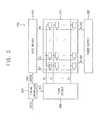
- FIGS. 1A and 1Bare diagrams illustrating a display device according to an embodiment of the inventive concept.
- FIG. 2is a block diagram illustrating an example of the display device of FIGS. 1A and 1B .
- FIG. 3is a block diagram illustrating an example of a display module included in the display device of FIG. 2 .
- FIG. 4is a circuit diagram illustrating an example of a pixel included in the display module of FIG. 3 .
- FIG. 5Ais a diagram illustrating a leakage current of transistors included in the pixel of FIG. 4 .
- FIG. 5Bis a diagram illustrating characteristics of silicon transistors included in the pixel of FIG. 4 .
- FIG. 5Cis a diagram illustrating an example in which the leakage current of FIG. 5A is changed according to a wavelength of infrared light.
- FIG. 6is a block diagram illustrating an example of an infrared sensing module included in the display device of FIG. 2 .
- FIGS. 7A and 7Bare diagrams illustrating an example of a display panel included in the display module of FIG. 3 .
- FIGS. 1A and 1Bare diagrams illustrating a display device according to an embodiment of the inventive concept.
- FIG. 2is a block diagram illustrating an example of the display device of FIGS. 1A and 1B .
- the display device 100may include a display module 110 , an infrared sensing module 120 , and an application processor 130 .
- the display device 100may be a smart phone.
- the display module 110may display an image based on image data.
- the display module 110may display the image on an entire region of its front surface (e.g., a surface of the display module 110 in a first direction D 1 ).
- the entire front surface(without a border or bezel) may be used for display of an image.
- the entire region of the front surface of the display module 110may be an active region in which pixels are arranged, and thus the display module 110 may not include a bezel (e.g., referred to as a dead space, an inactive region, etc) on its front surface.
- the infrared sensing module 120may be located on a back surface of the display module 110 (e.g., a rear surface of the display module 110 in a direction opposite to the first direction D 1 ).
- the infrared sensing module 120may be located between the display module 110 and a case 140 (or, a cover, a housing, etc).
- the case 140may provide an outward form of the display device 100 and may protect internal components (e.g., a battery, a memory device, etc) against external shocks (or, external stresses).
- the infrared sensing module 120may transmit first infrared light L 1 , may receive second infrared light L 2 , and may recognize an object 200 based on a change of the second infrared light L 2 .
- the first infrared light L 1may travel in the first direction D 1 and may pass through a first region A 1 of the display module 110 .
- the second infrared light L 2may include reflected light that is generated by at least a portion of the first infrared light L 1 being reflected off of the object 200 , may travel in the direction opposite to the first direction D 1 , and may pass through the first region A 1 of the display module 110 .
- the infrared sensing module 120may be arranged such that a portion from which the infrared light is transmitted may face the rear surface of the display panel to transmit the first infrared light through a portion of the display panel that exits the front surface of the display panel.
- the portion of the display panelmay be an active region, or another region having a lower pixel density than a remainder of the active region.
- the other regionmay be a region where the display panel is substantially transparent.
- the display device 100may have more than one infrared sensing module 120 .
- a plurality of infrared sensing modules 120could be located on or facing the rear surface of the display panel in areas having lower pixel density or transparency than an active region.
- infrared sensing modules 120could be arranged, as shown in FIG. 1A near upper and lower edges of the rear surface of the display panel.
- the infrared sensing modules 120may also be arranged along lateral edges of the rear surface of the display panel.
- the infrared sensing module 120may include one or more types of sensors, and the one or more types sensors may comprise, for example, a proximity sensor, a gesture sensor, a fingerprint recognition sensor, and/or an iris recognition sensor, etc., just to name some non-limiting possible examples of various types of sensors.
- the proximity sensormay detect a location of the object 200 (e.g., a distance between the object 200 and the display device 100 ) when the object 200 approaches the display device 100 .
- the gesture sensormay sense infrared lights (or, intensities of the infrared lights, infrared energies) of a plurality of points (e.g., a plurality of points on the front surface of the display device 100 ) and may detect a motion of the object 200 (or, a moving direction, a moving distance, a moving speed, a moving pattern, a gesture, etc) based on changes of the infrared lights.
- the fingerprint recognition sensormay generate an image of a fingerprint of a user based on the infrared light and may recognize the fingerprint of the user by analyzing a contrast pattern of the image.
- the iris recognition sensormay generate a picture of an iris of a user based on the infrared light and may recognize the iris of the user by analyzing a contrast pattern of the picture.
- the wavelength of the first infrared light L 1may be a wavelength greater than a predetermined value so that a luminance of light emitted by the pixel is not affected by operation of the infrared sensing module 120 .
- the predetermined value of the wavelengthmay be, for example, 1200 nm. However, the inventive concept is not limited to such a value.
- the first infrared light L 1may have a first wavelength of more than about 1200 nm.
- the first wavelength of the first infrared light L 1may be about 1300 nm.
- Each of the pixels arranged in the display module 110may include a transistor, and the transistor may have different characteristics according to a wavelength of incident light. For example, an amount of a leakage current that flows through the transistor (e.g., an amount of a current that flows through the transistor when the transistor is turned off) may change according to the wavelength of the incident light. These characteristics will be described in more detail with reference to FIGS. 4, 5A, 5B, and 5C .
- a pixel in the first region A 1 of the display module 110may emit light having luminance different from that of light emitted by a pixel in another region of the display module 110 (e.g., a region other than the first region A 1 in the display module 110 or a region through which only natural light passes).
- an amount (or, a rate) of a change in the leakage current of the transistor included in the first region A 1may be sharply reduced.
- the amount (or, a rate) of change in the leakage current of the transistor included in the first region A 1may stay the same (e.g. no change in the rate).
- a structure of the infrared sensing module 120will be described in detail with reference to FIG. 6 .
- the first wavelength of the first infrared light L 1will be described in detail with reference to FIGS. 5A through 5C .
- the application processor 130may include a function that executes application programs an operating system (OS) of the display device 100 (e.g., a smart phone, a tablet PC, etc) and a function that controls external system devices and/or interfaces.
- OSoperating system
- the application processor 130may control operation of the display module 110 and the infrared sensing module 120 .
- the application processor 130may stop an operation of the display module 110 when the infrared sensing module 120 recognizes the object 200 (or, when the object 200 approaches the display module 110 ).
- the application processor 130may stop an operation of the infrared sensing module 120 and may control the display module 110 to operate regardless of whether the object 200 is recognized.
- the display device 100may include the display module 110 that displays the image on the entire region of its front surface and the infrared sensing module 120 that is located on the rear (e.g. back) surface of a display panel of the display module 110 .
- the infrared sensing module 120may transmit the first infrared light L 1 that passes through the display module 110 and may recognize the object 200 based on the second infrared light L 2 that passes through the display module 110 .
- the first infrared light L 1has the first wavelength of more than 1200 nm
- the pixels in the first region A 1 of the display module 110may operate normally although the first infrared light L 1 passes through the first region A 1 of the display module 110 .
- the display device 100may display the image normally on its front surface (e.g. a front surface of a display panel) while including an infrared sensing function.
- FIG. 3is a block diagram illustrating an example of a display module included in the display device of FIG. 2 .
- FIG. 4is a circuit diagram illustrating an example of a pixel included in the display module of FIG. 3 .
- a structure of the display module 110will now be described in detail with reference to FIG. 3 .
- the display module 110may include a display panel 310 , a timing controller 320 , a scan driver 330 , and a data driver 340 .
- the timing controller 320may, for example, control the scan driver 330 and the data driver 340 by receiving input data (e.g., first data DATA 1 ) and input control signals (e.g., a horizontal synchronization signal, a vertical synchronization signal, and clock signals) from an external device, by generating image data (e.g., second data DATA 2 ) suitable for image displaying by a display panel of the display module 110 , and by generating a scan driving control signal SCS and a data driving control signal DCS based on the input control signals.
- input datae.g., first data DATA 1
- input control signalse.g., a horizontal synchronization signal, a vertical synchronization signal, and clock signals
- image datae.g., second data DATA 2
- the scan driver 330may generate a scan signal based on the scan driving control signal SCS received from the timing controller 320 .
- the scan driving control signal SCSmay include a start pulse and clock signals.
- the scan driver 330may include shift registers that sequentially generate the scan signal based on the start pulse and the clock signals.
- the data driver 340may generate a data signal based on the data driving control signal DCS.
- the data driver 340may convert the image data from a digital data signal into an analog data signal.
- the data driver 340may generate the data signal corresponding to the image data (e.g., data values included in the image data) based on predetermined gray-scale voltages (or, predetermined gamma voltages) and may sequentially provide the data signal to the display panel of the display module 110 .
- the display panel of display module 110may include scan-lines S 1 through Sn, data-lines D 1 through Dm, and pixels PX, where n and m are integers greater than or equal to 2.
- the pixels PXmay be arranged at locations corresponding to intersecting points of the scan-lines S 1 through Sn and the data-lines D 1 through Dm.
- Each of the pixels PXmay store the data signal that is provided through the data-lines D 1 through Dm in response to the scan signal that is provided through the scan-lines S 1 through Sn and may emit light based on the stored data signal.
- the display panel 310may be disposed on the front surface of the display module 110 (or, the display device 100 ), and thus only a front surface of the display panel 310 may be exposed to the outside.
- the timing controller 320 , the scan driver 330 , and the data driver 340may be located on a back (e.g. rear) surface of the display panel 310 .
- the pixel 400may include a light emitting element EL, a first transistor T 1 , a second transistor T 2 , and a storage capacitor Cst.
- the light emitting element ELmay be connected, for example, between a first power voltage ELVDD and a second power voltage ELVSS.
- the first power voltage ELVDDmay be greater than the second power voltage ELVSS.
- the light emitting element ELmay emit light based on an amount of a driving current that flows through the light emitting element EL between the first power voltage ELVDD and the second power voltage ELVSS.
- the light emitting element ELmay be an organic light emitting diode.
- the first and second power voltages ELVDD and ELVSSmay be generated by a power supply 350 illustrated in FIG. 3 .
- the first transistor T 1may include a first electrode that is connected to the first power voltage ELVDD, a second electrode that is connected to the light emitting element EL (e.g., an anode of the light emitting element EL), and a gate electrode that is connected to a first node N 1 .
- the first transistor T 1may control the driving current (e.g., an amount of the driving current) in response to a first node voltage of the first node N 1 to open and close the gate of the first transistor T 1 .
- the second transistor T 2may include a first electrode that receives the data signal Vdata, a second electrode that is connected to the first node N 1 , and a gate electrode that receives the scan signal scan[n].
- the second transistor T 2may transfer the data signal Vdata to the first node N 1 in response to a voltage level of the scan signal scan[n],
- the storage capacitor Cstmay be connected between the first node N 1 and the first power voltage ELVDD.
- the storage capacitor Cstmay store the data signal Vdata transferred via the second transistor T 2 .
- the pixel 400includes the first and second transistors T 1 and T 2 and the storage capacitor Cst
- the inventive conceptis not limited to pixels having the structure as pixel 400 .
- the pixel 400may have a 7 T- 1 C structure including seven transistors and one capacitor.
- the first and second transistors T 1 and T 2 of the pixel 400are implemented by P-type transistors
- the first and second transistors T 1 and T 2 of the pixel 400may be implemented by N-type transistors.
- the aforementionedare just a few of the possible arrangements according to the inventive concept.
- the pixel 400may exhibit different characteristics according to a particular wavelength of light that enters (or, passes through) the pixel 400 (e.g., incident light). For example, even when the pixel 400 receives the same data signal, the pixel 400 may emit light having different luminance according to the wavelength of the incident light. For example, luminance implemented by a pixel to which infrared light having a wavelength of 940 nm (e.g., infrared light transmitted by a conventional infrared sensor) is applied may be different from luminance implemented by the pixel to which natural light is applied.
- infrared light having a wavelength of 940 nme.g., infrared light transmitted by a conventional infrared sensor
- the pixel 400includes the light emitting element EL, the first and second transistors T 1 and T 2 , and the storage capacitor Cst
- a change in characteristics of the pixel 400may be caused by the light emitting element EL, the first and second transistors T 1 and T 2 , and the storage capacitor Cst.
- the change in characteristics of the pixel 400will be described in detail with reference to experimental examples.
- first luminancee.g., reference luminance
- first luminanceimplemented by the light emitting element EL of the pixel 400
- the infrared light having the wavelength of 940 nmwas applied to just the light emitting element EL of the pixel 400
- a second luminance implemented by the light emitting element EL of the pixel 400was measured.
- the first luminancewas equal to the second luminance.
- the second luminance implemented by the light emitting element EL of the pixel 400was measured by changing the wavelength of the infrared light that is applied to the light emitting element EL of the pixel 400 among various wavelengths, which were, for example 625 nm, 880 nm, 970 nm, 1050 nm, 1200 nm, 1300 nm, and 1450 nm. In this case, the first luminance was equal to the second luminance.
- the light emitting element EL of the pixel 400was not affected by the infrared light (e.g., the wavelength of the infrared light).
- the infrared lightwas applied to just the storage capacitor Cst of the pixel 400 .
- the second luminance implemented by the light emitting element EL of the pixel 400was measured by changing the wavelength of the infrared light that is applied to the storage capacitor Cst of the pixel 400 .
- the first luminancewas equal to the second luminance.
- the storage capacitor Cst of the pixel 400was not affected by the infrared light (e.g., the wavelength of the infrared light).
- a first leakage current of the first transistor T 1 of the pixel 400(e.g., a leakage current flowing through the first transistor T 1 when the first transistor T 1 is turned off) was measured.
- a second leakage current of the first transistor T 1 of the pixel 400was measured, and a graph is provided to illustrate the response.
- FIG. 5Ais a diagram illustrating a leakage current of transistors included in the pixel of FIG. 4 .
- a gate voltage VGSrefers to a voltage applied to a gate electrode of the first transistor T 1 (or a voltage between the gate electrode and a source electrode in the first transistor T 1 ), and a current IDS refers to a current flowing through the first transistor T 1 .
- the first curve G 1indicates the first current flowing through the first transistor T 1 when the infrared light was not applied to the pixel 400 .
- the second curve G 2indicates the second current flowing through the first transistor T 1 when the infrared light having the wavelength of 940 nm was applied to only the first transistor T 1 .
- the second currentwas equal to the first current when the gate voltage VGS was less than ⁇ 5 volt (V), more accurately, less than ⁇ 3 volt (e.g., when the P-type transistor was turned on).
- the second currentwas different from the first current when the gate voltage VGS was more than ⁇ 0 volt, more accurately, more than ⁇ 3 volt (e.g., when the P-type transistor is turned off).
- the second currentwas about 1 .E-14 (e.g., 10 ⁇ 14 ) ampere (A) and the first current was about 1 .E-11 (e.g., 10 ⁇ 11 ) ampere.
- the leakage current of the first transistor T 1was increased.
- the first transistor T 1 of the pixel 400was affected by the infrared light (e.g., the wavelength of the infrared light).
- the second transistor 12was experimented under the same condition as that of the third experimental example. As a result, the leakage current of the second transistor 12 was similar to the leakage current of the first transistor T 1 . In conclusion, from the third experimental example and FIG. 5A , it was confirmed that the second transistor T 2 of the pixel 400 was affected by the wavelength of infrared light.
- the first and second transistors T 1 and T 2may include silicon (Si), and the silicon may absorb light having a specific wavelength band.
- Sisilicon
- the siliconmay absorb light having a specific wavelength band.
- FIG. 5Bis a diagram illustrating characteristics of silicon of transistors included in the pixel of FIG. 4 .
- a third curve G 3indicates an ideal spectral response of the silicon
- a fourth curve G 4indicates an actual spectral response of the silicon.
- the siliconabsorbed light having a first wavelength band between 0 micrometer ( ⁇ m) (or, in some embodiments of the inventive concept, 0.01 pm or 10 nanometer (nm)) and 1.1 ⁇ m along the third curve G 3 . As a wavelength was longer in the first wavelength band, an amount of light absorbed by the silicon was increased.
- the siliconabsorbed light having a second wavelength band between 0.4 ⁇ m (or, 400 nm) and 1.2 ⁇ m (or, 1200 nm) along the fourth curve G 4 ,
- the siliconabsorbed most of light having a wavelength of 1 ⁇ m, and thus an absorption amount of light having a wavelength of more than 1 pm was sharply decreased.
- the energy gap (or, band gap) of the siliconwas 1.12 electron volt (eV) corresponding to light having a wavelength of about 1.1
- the fourth experimental examplewas repeatedly performed by changing the wavelength of the infrared light.
- the first leakage current of the first transistor T 1(e.g., the leakage current flowing through the first transistor T 1 when the first transistor T 1 was turned off) was measured.
- the second leakage current of the first transistor T 1was measured, Here, the second leakage current was repeatedly measured by changing the wavelength of the infrared light among 625 nm, 880 nm, 970 nm, 1050 nm, 1200 nm, 1300 nm, and 1450 nm.
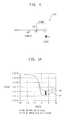
- FIG. 5Cis a diagram illustrating an example in which the leakage current of FIG. 5A is changed according to a wavelength of infrared light.
- a fifth curve G 5indicates a current difference ⁇ IOFF between a first leakage current and a second leakage current according to a wavelength.
- the current difference ⁇ IOFFwas 1 .E-13 ampere when the wavelength of the infrared light was 625 nm
- the current difference ⁇ IOFFwas reduced when the wavelength of the infrared light was 1050 nm
- the current difference ⁇ IOFFwas sharply reduced when the wavelength of the infrared light was 1200 nm (e.g., the current difference ⁇ IOFF when the wavelength of the infrared light was 1200 nm was less than 1/20 of the current difference ⁇ IOFF when the wavelength of the infrared light was 1050 nm)
- the current difference A IOFFwas less than 1.E-16 (or, zero) ampere when the wavelength of the infrared light was more than 1300 nm (e.g., 1300 nm, 1450 nm, etc).
- the current difference ⁇ IOFF when the wavelength of the infrared light was 625 nmhad the greatest value
- the current difference ⁇ IOFF shown in FIG. 5C when the wavelength of the infrared light was 1200 nmwas significantly reduced as compared to the current difference ⁇ IOFF when the wavelength of the infrared light was less than 1200 nm.
- the leakage current of the first transistor T 1was not changed when the wavelength of the infrared light was more than 1300 nm.
- the first infrared light L 1may have a wavelength included in a wavelength band between 1200 nm and 1400 nm corresponding to a range of energy reduction of less than 30%.
- the first infrared light L 1may have a wavelength of 1200 nm.
- the energy of the first infrared light L 1may be maximized while minimizing an amount (or, a rate) of a change in the leakage current of the first and second transistors T 1 and T 2 included in the pixel 400 (or, while controlling a change in luminance implemented by the pixel 400 not to be perceived by a user).
- the first infrared light L 1may have a wavelength of 1300 nm. In this case, the energy of the first infrared light L 1 may be maximized while preventing the change in the leakage current of the first and second transistors T 1 and T 2 included in the pixel 400 .
- the leakage current of the first and second transistors T 1 and T 2may not change when the first infrared light L 1 has a wavelength of more than 1200 nm.
- the pixel 400may emit light normally when the first infrared light L 1 has a wavelength of more than 1200 nm.
- the sensing performance of the infrared sensing module 120may be maximized while controlling the change in luminance implemented by the pixel 400 not to be perceived by the user. Further, when the first infrared light L 1 has a wavelength of 1300 nm, the first infrared light L 1 may not affect the pixel 400 .
- FIG. 6is a block diagram illustrating an example of an infrared sensing module included in the display device of FIG. 2 .
- the infrared sensing module 120may include, for example, an infrared sensor 610 and an infrared sensing controller 620 .
- the infrared sensor 610may include an infrared light emitting element 611 and an infrared sensing element 612 .
- the infrared light emitting element 611may output (or, transmit) the first infrared light L 1 .
- the infrared light emitting element 611may be an infrared light emitting diode, and the first infrared light L 1 having a wavelength of more than 1200 nm may be output.
- the infrared light emitting element 611may be located within a sensor case 613 .
- the infrared light emitting element 611may output the first infrared light L 1 in a specific direction (e.g., in the first direction D 1 as illustrated in FIG. 1B ).
- the infrared sensing element 612may measure (or, sense) intensity of the second infrared light L 2 to generate a measurement signal.
- the second infrared light L 2may include reflected light that is generated by the first infrared light L 1 being reflected by the object 200 .
- the infrared sensing element 612may be located within the sensor case 613 .
- the infrared sensing element 612may be located in a space that is different from a space in which the infrared light emitting element 611 is located, where the space in which the infrared sensing element 612 is located may be separated, by an optical wall 614 , from the space in which the infrared light emitting element 611 is located.
- the infrared sensing element 61may be an infrared image-pickup element or an infrared imaging element.
- the infrared sensing element 612may include a plurality of sensing elements and may generate a two-dimensional (2D) infrared image.
- the infrared sensing module 120may be a fingerprint recognition sensor or an iris recognition sensor.
- the infrared sensor 610may further include a condensing lens.
- the condensing lensmay be disposed over the infrared light emitting element 611 (or, on the path along which the first infrared light L 1 output from the infrared light emitting element 611 travels). In this case, the energy of the first infrared light L 1 may be strengthened (or, increased).
- the infrared sensor 610may further include a first infrared transmission (or, a penetration) filter 615 .
- the first infrared transmission filter 615may be disposed over the infrared light emitting element 611 (or, on the path along which the first infrared light L 1 output from the infrared light emitting element 611 travels).
- the first infrared transmission filter 615may allow only the first infrared light L 1 having a wavelength of more than 1200 nm (or, 1300 nm) to pass through.
- the infrared light emitting element 611may emit third infrared light having a wavelength of less than 1200 nm, but the infrared sensor 610 may emit only the first infrared light having a wavelength of more than 1200 nm using the first infrared transmission filter 615 .
- the infrared sensor 610may further include, for example, a second infrared transmission filter 616 .
- the second infrared transmission filter 616may be disposed over the infrared sensing element 612 (or, on the path along which the second infrared light L 2 input to the infrared sensing element 612 travels).
- the second infrared transmission filter 616may allow only fourth infrared light L 4 (e.g., the reflected light that is generated by the first infrared light L 1 being reflected by the object) having a wavelength of more than 1200 nm (or, 1300 nm) to pass through.
- the infrared sensing element 612may generate (or, output) the measurement signal through more simple processes.
- the infrared sensing element 612may exclude a process of extracting the reflected light from the second infrared light L 2 .
- the infrared sensing controller 620may control an operation of the infrared sensor 610 and may recognize the object 200 based on the measurement signal (or, a change of the measurement signal). For example, the infrared sensing controller 620 may control an operating state, an operating cycle, etc of the infrared sensor 610 based on a control signal that is externally provided (e.g., a control signal that is provide from the application processor 130 of FIG. 2 ). In addition, as described above with reference to FIG.
- the infrared sensing controller 620may recognize (or, detect) a location of the object 200 (e.g., a distance between the object 200 and the display device 100 ) based on the measurement signal or may recognize a motion (or, movement) of the object 200 based on the change of the measurement signal.
- the infrared sensing element 612is the infrared image-pickup element, the infrared sensing element 612 may recognize a specific pattern (e.g., a fingerprint pattern, an iris pattern, etc) from an infrared image.
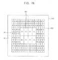
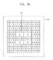
- FIGS. 7A and 7Bare diagrams illustrating an example of a display panel 310 included in the display module 110 of FIG. 3 .
- first pixel density of the first region A 1may be lower than second pixel density of the second region A 2 .
- the first infrared light L 1may be applied to the first region A 1 .
- the second region A 2may be a region other than the first region A 1 .
- a size of a first pixel PX 1 included in the first region A 1may be bigger than a size of a second pixel PX 2 included in the second region A 2 .
- the size of the first pixel PX 1may be four times bigger than the size of the second pixel PX 2 .
- the first pixel PX 1 and the second pixel PX 2include an identical pixel circuit (e.g., the transistors T 1 and T 2 , the light emitting element EL, etc included in the pixel 400 illustrated in FIG. 4 ). But, the first pixel PX 1 may further include an empty space in which components like wirings, transistors, etc are not formed. Thus, the light passing through the empty space of the first pixel PX 1 may not be reflected or blocked by the components.
- the first region A 1may include a transmission region TA (or, a transmission window).
- the transmission region TA of the first region A 1may have transmittance higher than transmittance of the second region A 2 (or, a region in which sub pixels R, G, and B that emit first color light, second color light, and third color light, respectively are formed).
- the transmission region TAmay be located near the sub pixels R, G, and B, and the pixel circuit (e.g., electrodes, wirings, transistors, etc) may not be formed in the transmission region TA.
- an area of the transmission region TAmay be about 20%-90% of an area of the first region A 1 .
- the first region A 1may be partially transparent. Thus, most of the first infrared light L 1 input to the transmission region TA may pass through the transmission region TA.
- the display panel 310(or, the first region A 1 ) may be partially transparent and thus sensing performance (or, sensing accuracy, recognition rate) of the infrared sensing module 120 may be enhanced.
- the first pixel density of the first region A 1 through which the first infrared light L 1 passesmay be lower than a pixel density of another region.
- the first region Amay be partially transparent.
- transmittance of the first infrared light L 1may be enhanced (or, increased), and thus the recognition rate of the infrared sensing module 120 may be prevented from being degraded (or, decreased).
- the present inventive conceptmay be applied to a display device and various display systems including the display device.
- the present inventive conceptmay be applied to a television, a computer monitor; a laptop, a digital camera, a cellular phone, a smart phone, a video phone, a smart pad, a smart watch, a tablet PC, a car navigation system, a personal digital assistants (PDA), a portable multimedia player (PMP), an MP3 player, etc.
- PDApersonal digital assistants
- PMPportable multimedia player
- MP3 playeretc.
Landscapes
- Engineering & Computer Science (AREA)
- Physics & Mathematics (AREA)
- Theoretical Computer Science (AREA)
- General Physics & Mathematics (AREA)
- General Engineering & Computer Science (AREA)
- Human Computer Interaction (AREA)
- Remote Sensing (AREA)
- Radar, Positioning & Navigation (AREA)
- Computer Networks & Wireless Communication (AREA)
- Chemical & Material Sciences (AREA)
- Inorganic Chemistry (AREA)
- Electromagnetism (AREA)
- Sustainable Development (AREA)
- Life Sciences & Earth Sciences (AREA)
- Computer Hardware Design (AREA)
- Spectroscopy & Molecular Physics (AREA)
- Signal Processing (AREA)
- Microelectronics & Electronic Packaging (AREA)
- Geometry (AREA)
- Optics & Photonics (AREA)
- Multimedia (AREA)
- Control Of Indicators Other Than Cathode Ray Tubes (AREA)
- Electroluminescent Light Sources (AREA)
- Transforming Light Signals Into Electric Signals (AREA)
Abstract
Description
- This application claims priority under 35 U.S.C. § 119 from Korean Patent Application No. 10-2016-0146864, filed on Nov. 4, 2016 in the Korean Intellectual Property Office (KIPO), the contents of which are incorporated by reference herein.
- Embodiments of the inventive concept relate generally to a display device. More particularly, embodiments of the present inventive concept relate to a display device that includes an infrared sensor.
- A display device displays an image using a pixel (or, a pixel circuit). Some display devices include an infrared sensor in a bezel (or, in an edge region) of its front surface (e.g., a surface on which the image is displayed). In such an arrangement, the display device can recognize an object within a predetermined distance from the display device via the infrared sensor. For example, the display device may transmit infrared light, may receive reflected light that is generated by the infrared light being reflected off of the object, may calculate a distance between the display device and the object based on intensity of the reflected light. Moreover, the display device may not display the image if the calculated distance is less than a specific distance.
- Generally, as the bezel of the display device decreases, the eyes of a user may focus more on the image (or, a screen of the display device). Recently, many manufacturers have reduced the size of, or eliminated the bezel altogether from the front surface of the display device. When the display device does not include the bezel on the front surface of the display device, the display device can use the front surface of the display device more efficiently, for example, by displaying the image on an entire region of the front surface of the display device. In such a case, the infrared sensor may be relocated to another location of the display device.
- In an embodiment, the inventive concept may provide a display device that can display an image on an entire region of its front surface while including an infrared sensing function.
- According to an embodiment of the inventive concept, a display device may include a display panel having a front surface and a rear surface, the display panel including an active region in which a pixel that emits light based on a data signal is disposed; and an infrared sensing module configured to transmit infrared light including at least a first infrared light that passes in a first direction away from the front surface of the display panel and through the active region, and the infrared sensing module is configured to receive a second infrared light that passes in a second direction toward the front surface of the display panel and through the active region by which the infrared sensing module recognizes an object external to the display device.
- According to an embodiment of the inventive concept, the infrared sensing module is arranged on a rear surface of the display panel, and the infrared sensing module transmits the first infrared light in a first direction that is substantially perpendicular to the front surface of the display panel.
- The infrared sensing module may be arranged to face the rear surface of the display panel to transmit the first infrared light through a portion of the active region of the display panel having a lower pixel density than a remainder of the active region.
- The display device may further include a housing having a surface that faces the rear surface of the display panel, and wherein the infrared sensing module is arranged between the rear surface of the display panel and the housing.
- According to an embodiment of the inventive concept, the second infrared light may include reflected light that is generated by the first infrared light being reflected by the object. In addition, the infrared sensing module may recognize the object based on a change of the second infrared light.
- According to an embodiment of the inventive concept, the infrared sensing module may include at least one selected from a proximity sensor, a gesture sensor, and a fingerprint recognition sensor. According to an embodiment of the inventive concept, the first infrared light may have a first wavelength of more than about 1200 nm.
- According to an embodiment of the inventive concept, a luminance of the pixel located in the active region is unchanged when the infrared sensing module transmits the first infrared light at the wavelength of greater than about 1200 nm.
- According to an embodiment of the inventive concept, the first wavelength of the first infrared light may be 1300 nm.
- According to an embodiment of the inventive concept, the pixel may include at least one transistor including silicon. In addition, the first infrared light may have a first wavelength that is out of a wavelength band of light that is absorbed by the silicon.
- According to an embodiment of the inventive concept, the display device may further include a scan driver configured to generate a scan signal, and a data driver configured to generate the data signal based on image data that is provided from an external device. In addition, the pixel may include a light emitting element connected between a first power voltage and a second power voltage, a first transistor configured to control a driving current that flows through the light emitting element in response to a first node voltage of a first node, a second transistor configured to transfer the data signal to the first node in response to the scan signal, and a storage capacitor connected to the first node and configured to store the data signal. Further, the at least one transistor may include the first transistor and the second transistor.
- According to an embodiment of the inventive concept, a first leakage current may flow through the at least one transistor in a turned-off state when the first infrared light is applied to the active region, a second leakage current may flow through the at least one transistor in the turned-off state when natural light is applied to the active region, and a difference between the first leakage current and the second leakage current may be smaller than or equal to a reference value by the first wavelength of the first infrared light.
- According to an embodiment of the inventive concept, the infrared sensing module may include an infrared light emitting element configured to emit the first infrared light, an infrared sensing element configured to measure intensity of the second infrared light to output a measurement signal, and an infrared sensing controller configured to recognize the object based on a change of the measurement signal.
- According to an embodiment of the inventive concept, the infrared sensing module may further include a condensing lens configured to condense and output the first infrared light.
- According to an embodiment of the inventive concept, the infrared sensing module may include an infrared light emitting element configured to emit third infrared light, a first infrared transmission filter configured to pass the first infrared light included in the third. infrared light, an infrared sensing element configured to measure intensity of the second infrared light to output a measurement signal, and an infrared sensing controller configured to recognize the object based on a change of the measurement signal.
- According to an embodiment of the inventive concept, the infrared sensing module may further include a second infrared transmission filter configured to pass fourth infrared light included in the second infrared light, the fourth infrared light having a wavelength that is equal to a wavelength of the first infrared light. In addition, the infrared sensing element may measure intensity of the fourth infrared light.
- According to an embodiment of the inventive concept, the display panel may include a first region through which the first infrared light passes, and first pixel density of the first region may be lower than second pixel density of a second region that is different from the first region.
- According to an embodiment of the inventive concept, the first region may include a transmission region having transmittance that is higher than transmittance of the second region.
- According to an embodiment of the inventive concept, a display device may include a display panel including an active region in which a pixel that emits light based on a data signal is disposed, and an infrared sensing module configured to transmit first infrared light that passes through the active region and to receive second infrared light that passes through the active region to recognize an object. Here, the pixel may include at least one transistor that operates in response to the data signal, and a current that flows through the at least one transistor when the at least one transistor is turned off is changed according to a change in a wavelength of light that is applied to the active region. In addition, the first infrared light may have a first wavelength by which a change rate of the current is smaller than or equal to a reference value.
- According to an embodiment of the inventive concept, the infrared sensing module may include at least one selected from a proximity sensor, a gesture sensor, and a fingerprint recognition sensor.
- According to an embodiment of the inventive concept, the at least one transistor may include (e.g. may be comprised of) silicon. In addition, the first wavelength of the first infrared light may have a wavelength that is out of a band of wavelengths of light that the silicon absorbs.
- According to an embodiment of the inventive concept, the first wavelength of the first infrared light may be greater than 1200 nm.
- According to an embodiment of the inventive concept, the first wavelength of the first infrared light may be about 1300 nm.
- Therefore, a display device according to example embodiments may include a display module that displays an image on an entire region of its front surface and an infrared sensing module that is located on a back surface of the display module. Here, the infrared sensing module may transmit first infrared light that passes through the display module to go the outside of the display device (e.g., an exterior) and may recognize an object based on second infrared light that passes through the display module to go inside the display device (e.g. an interior), where one or more various types of sensors detect, for example, the presence of an object external to the display device, and/or various attributes or characteristics of the object, including but not limited to distance from the display device, gestures, biometric information (included but not limited to fingerprint, iris, facial scanning). In particular, since the first infrared light may have a first wavelength of more than 1200 nm (e.g., 1200 nm, 1300 nm, etc), luminance of a pixel located in a specific region of the display module may not be changed although the first infrared light passes through the specific region of the display module. Thus, the display device may display the image normally on the front surface of the display device while including an infrared sensing function.
- In addition, in the display device, the specific region of the display module (e.g., a portion of a display panel) through which the first infrared light passes may have relatively low pixel density or may be partially transparent. Thus, transmittance of the first infrared light may be enhanced and thus recognition of the display device for the object may be increased.
- According to an embodiment of the inventive concept, a display panel may include an active region in which a pixel is disposed, the pixel emits light based on a data signal; and an infrared sensing module configured to transmit a first infrared light that passes through the active region to exit the display device, and to receive a second infrared light that enters the display device and passes through the active region to recognize an object. The pixel may include at least one transistor that operates in response to receiving the data signal, and a current that flows through the at least one transistor when the at least one transistor is turned off is changed according to a change in a wavelength of light that is applied to the active region. The first infrared light may have a first wavelength having a change rate of the current that is less than or equal to a reference value.
- One or more illustrative, non-limiting embodiments will be better appreciated by a person of ordinary skill in the art from the following detailed description taken in conjunction with the accompanying drawings.
FIGS. 1A and 1B are diagrams illustrating a display device according to an embodiment of the inventive concept.FIG. 2 is a block diagram illustrating an example of the display device ofFIGS. 1A and 1B .FIG. 3 is a block diagram illustrating an example of a display module included in the display device ofFIG. 2 .FIG. 4 is a circuit diagram illustrating an example of a pixel included in the display module ofFIG. 3 .FIG. 5A is a diagram illustrating a leakage current of transistors included in the pixel ofFIG. 4 .FIG. 5B is a diagram illustrating characteristics of silicon transistors included in the pixel ofFIG. 4 .FIG. 5C is a diagram illustrating an example in which the leakage current ofFIG. 5A is changed according to a wavelength of infrared light.FIG. 6 is a block diagram illustrating an example of an infrared sensing module included in the display device ofFIG. 2 .FIGS. 7A and 7B are diagrams illustrating an example of a display panel included in the display module ofFIG. 3 .- Hereinafter, embodiments of the present inventive concept will be explained in detail with reference to the accompanying drawings.
FIGS. 1A and 1B are diagrams illustrating a display device according to an embodiment of the inventive concept.FIG. 2 is a block diagram illustrating an example of the display device ofFIGS. 1A and 1B .- Referring now to
FIGS. 1A, 1B, and 2 , thedisplay device 100 may include adisplay module 110, aninfrared sensing module 120, and anapplication processor 130. For example, thedisplay device 100 may be a smart phone. - The
display module 110 may display an image based on image data. Here, thedisplay module 110 may display the image on an entire region of its front surface (e.g., a surface of thedisplay module 110 in a first direction D1). The entire front surface (without a border or bezel) may be used for display of an image. In other words, the entire region of the front surface of thedisplay module 110 may be an active region in which pixels are arranged, and thus thedisplay module 110 may not include a bezel (e.g., referred to as a dead space, an inactive region, etc) on its front surface. - The infrared sensing module120 (shown in
FIG. 1B ) may be located on a back surface of the display module110 (e.g., a rear surface of thedisplay module 110 in a direction opposite to the first direction D1). In other words, theinfrared sensing module 120 may be located between thedisplay module 110 and a case140 (or, a cover, a housing, etc). Here, thecase 140 may provide an outward form of thedisplay device 100 and may protect internal components (e.g., a battery, a memory device, etc) against external shocks (or, external stresses). - The
infrared sensing module 120 may transmit first infrared light L1, may receive second infrared light L2, and may recognize anobject 200 based on a change of the second infrared light L2. Here, the first infrared light L1 may travel in the first direction D1 and may pass through a first region A1 of thedisplay module 110. In addition, the second infrared light L2 may include reflected light that is generated by at least a portion of the first infrared light L1 being reflected off of theobject 200, may travel in the direction opposite to the first direction D1, and may pass through the first region A1 of thedisplay module 110. - The
infrared sensing module 120 may be arranged such that a portion from which the infrared light is transmitted may face the rear surface of the display panel to transmit the first infrared light through a portion of the display panel that exits the front surface of the display panel. The portion of the display panel may be an active region, or another region having a lower pixel density than a remainder of the active region. For example, the other region may be a region where the display panel is substantially transparent. An artisan should understand and appreciate that thedisplay device 100 may have more than oneinfrared sensing module 120. A plurality ofinfrared sensing modules 120 could be located on or facing the rear surface of the display panel in areas having lower pixel density or transparency than an active region. For example,infrared sensing modules 120 could be arranged, as shown inFIG. 1A near upper and lower edges of the rear surface of the display panel. Theinfrared sensing modules 120 may also be arranged along lateral edges of the rear surface of the display panel. - In an embodiment of the inventive concept, the
infrared sensing module 120 may include one or more types of sensors, and the one or more types sensors may comprise, for example, a proximity sensor, a gesture sensor, a fingerprint recognition sensor, and/or an iris recognition sensor, etc., just to name some non-limiting possible examples of various types of sensors. Moreover, for example, the proximity sensor may detect a location of the object200 (e.g., a distance between theobject 200 and the display device100) when theobject 200 approaches thedisplay device 100. The gesture sensor, for example, may sense infrared lights (or, intensities of the infrared lights, infrared energies) of a plurality of points (e.g., a plurality of points on the front surface of the display device100) and may detect a motion of the object200 (or, a moving direction, a moving distance, a moving speed, a moving pattern, a gesture, etc) based on changes of the infrared lights. The fingerprint recognition sensor may generate an image of a fingerprint of a user based on the infrared light and may recognize the fingerprint of the user by analyzing a contrast pattern of the image. The iris recognition sensor may generate a picture of an iris of a user based on the infrared light and may recognize the iris of the user by analyzing a contrast pattern of the picture. - The wavelength of the first infrared light L1 may be a wavelength greater than a predetermined value so that a luminance of light emitted by the pixel is not affected by operation of the
infrared sensing module 120. The predetermined value of the wavelength may be, for example, 1200 nm. However, the inventive concept is not limited to such a value. - For example, in at least one embodiment of the inventive concept, the first infrared light L1 may have a first wavelength of more than about 1200 nm. For example, the first wavelength of the first infrared light L1 may be about 1300 nm.
- Each of the pixels arranged in the
display module 110 may include a transistor, and the transistor may have different characteristics according to a wavelength of incident light. For example, an amount of a leakage current that flows through the transistor (e.g., an amount of a current that flows through the transistor when the transistor is turned off) may change according to the wavelength of the incident light. These characteristics will be described in more detail with reference toFIGS. 4, 5A, 5B, and 5C . Accordingly, based on the same data signal, a pixel in the first region A1 of thedisplay module 110, where the first and second infrared lights L1 and L2 pass through the first region A1 of thedisplay module 110, may emit light having luminance different from that of light emitted by a pixel in another region of the display module110 (e.g., a region other than the first region A1 in thedisplay module 110 or a region through which only natural light passes). - When the first infrared light L1 has the first wavelength of greater than 1200 nm, an amount (or, a rate) of a change in the leakage current of the transistor included in the first region A1 may be sharply reduced. In addition, when the first infrared light L1 has the first wavelength of 1300 nm, the amount (or, a rate) of change in the leakage current of the transistor included in the first region A1 may stay the same (e.g. no change in the rate).
- A structure of the
infrared sensing module 120 will be described in detail with reference toFIG. 6 . The first wavelength of the first infrared light L1 will be described in detail with reference toFIGS. 5A through 5C . - The
application processor 130 may include a function that executes application programs an operating system (OS) of the display device100 (e.g., a smart phone, a tablet PC, etc) and a function that controls external system devices and/or interfaces. - In an embodiment of the inventive concept, the
application processor 130 may control operation of thedisplay module 110 and theinfrared sensing module 120. For example, theapplication processor 130 may stop an operation of thedisplay module 110 when theinfrared sensing module 120 recognizes the object200 (or, when theobject 200 approaches the display module110). For example, theapplication processor 130 may stop an operation of theinfrared sensing module 120 and may control thedisplay module 110 to operate regardless of whether theobject 200 is recognized. - In brief, the
display device 100 may include thedisplay module 110 that displays the image on the entire region of its front surface and theinfrared sensing module 120 that is located on the rear (e.g. back) surface of a display panel of thedisplay module 110. Theinfrared sensing module 120 may transmit the first infrared light L1 that passes through thedisplay module 110 and may recognize theobject 200 based on the second infrared light L2 that passes through thedisplay module 110. Here, since the first infrared light L1 has the first wavelength of more than 1200 nm, the pixels in the first region A1 of thedisplay module 110 may operate normally although the first infrared light L1 passes through the first region A1 of thedisplay module 110. Thus, thedisplay device 100 may display the image normally on its front surface (e.g. a front surface of a display panel) while including an infrared sensing function. FIG. 3 is a block diagram illustrating an example of a display module included in the display device ofFIG. 2 .FIG. 4 is a circuit diagram illustrating an example of a pixel included in the display module ofFIG. 3 . A structure of thedisplay module 110 will now be described in detail with reference toFIG. 3 .- Referring to
FIG. 3 , thedisplay module 110 may include adisplay panel 310, atiming controller 320, ascan driver 330, and adata driver 340. - The
timing controller 320 may, for example, control thescan driver 330 and thedata driver 340 by receiving input data (e.g., first data DATA1) and input control signals (e.g., a horizontal synchronization signal, a vertical synchronization signal, and clock signals) from an external device, by generating image data (e.g., second data DATA2) suitable for image displaying by a display panel of thedisplay module 110, and by generating a scan driving control signal SCS and a data driving control signal DCS based on the input control signals. - The
scan driver 330 may generate a scan signal based on the scan driving control signal SCS received from thetiming controller 320. The scan driving control signal SCS may include a start pulse and clock signals. Thescan driver 330 may include shift registers that sequentially generate the scan signal based on the start pulse and the clock signals. - The
data driver 340 may generate a data signal based on the data driving control signal DCS. Thedata driver 340 may convert the image data from a digital data signal into an analog data signal. Thedata driver 340 may generate the data signal corresponding to the image data (e.g., data values included in the image data) based on predetermined gray-scale voltages (or, predetermined gamma voltages) and may sequentially provide the data signal to the display panel of thedisplay module 110. - With continued reference to
FIG. 3 , the display panel ofdisplay module 110 may include scan-lines S1 through Sn, data-lines D1 through Dm, and pixels PX, where n and m are integers greater than or equal to 2. The pixels PX may be arranged at locations corresponding to intersecting points of the scan-lines S1 through Sn and the data-lines D1 through Dm. Each of the pixels PX may store the data signal that is provided through the data-lines D1 through Dm in response to the scan signal that is provided through the scan-lines S1 through Sn and may emit light based on the stored data signal. - The
display panel 310 may be disposed on the front surface of the display module110 (or, the display device100), and thus only a front surface of thedisplay panel 310 may be exposed to the outside. In addition, thetiming controller 320, thescan driver 330, and thedata driver 340 may be located on a back (e.g. rear) surface of thedisplay panel 310. - Referring now to
FIG. 4 , thepixel 400 may include a light emitting element EL, a first transistor T1, a second transistor T2, and a storage capacitor Cst. - The light emitting element EL may be connected, for example, between a first power voltage ELVDD and a second power voltage ELVSS. Here, the first power voltage ELVDD may be greater than the second power voltage ELVSS. The light emitting element EL may emit light based on an amount of a driving current that flows through the light emitting element EL between the first power voltage ELVDD and the second power voltage ELVSS. In addition, the light emitting element EL, may be an organic light emitting diode. However, a person of ordinary skill in the art should understand and appreciate that the inventive concept is not limited to a particular type of light emitting element. Here, the first and second power voltages ELVDD and ELVSS may be generated by a
power supply 350 illustrated inFIG. 3 . - The first transistor T1 may include a first electrode that is connected to the first power voltage ELVDD, a second electrode that is connected to the light emitting element EL (e.g., an anode of the light emitting element EL), and a gate electrode that is connected to a first node N1. The first transistor T1 may control the driving current (e.g., an amount of the driving current) in response to a first node voltage of the first node N1 to open and close the gate of the first transistor T1.
- The second transistor T2 may include a first electrode that receives the data signal Vdata, a second electrode that is connected to the first node N1, and a gate electrode that receives the scan signal scan[n]. The second transistor T2 may transfer the data signal Vdata to the first node N1 in response to a voltage level of the scan signal scan[n],
- The storage capacitor Cst may be connected between the first node N1 and the first power voltage ELVDD. The storage capacitor Cst may store the data signal Vdata transferred via the second transistor T2.
- Although it is illustrated in
FIG. 4 that thepixel 400 includes the first and second transistors T1 and T2 and the storage capacitor Cst, the inventive concept is not limited to pixels having the structure aspixel 400. For example, thepixel 400 may have a7T-1C structure including seven transistors and one capacitor. Although it is illustrated inFIG. 4 that the first and second transistors T1 and T2 of thepixel 400 are implemented by P-type transistors, the first and second transistors T1 and T2 of thepixel 400 may be implemented by N-type transistors. The aforementioned are just a few of the possible arrangements according to the inventive concept. - As described above, the
pixel 400 may exhibit different characteristics according to a particular wavelength of light that enters (or, passes through) the pixel400 (e.g., incident light). For example, even when thepixel 400 receives the same data signal, thepixel 400 may emit light having different luminance according to the wavelength of the incident light. For example, luminance implemented by a pixel to which infrared light having a wavelength of 940 nm (e.g., infrared light transmitted by a conventional infrared sensor) is applied may be different from luminance implemented by the pixel to which natural light is applied. - In the embodiment shown in
FIG. 4 , a person of ordinary skill in the art should appreciate that thepixel 400 includes the light emitting element EL, the first and second transistors T1 and T2, and the storage capacitor Cst, a change in characteristics of thepixel 400 may be caused by the light emitting element EL, the first and second transistors T1 and T2, and the storage capacitor Cst. Hereinafter, the change in characteristics of thepixel 400 will be described in detail with reference to experimental examples. - First Experimental Example
- In a first case where infrared light was not applied to the pixel400 (or, when only the natural light is applied to the pixel400), first luminance (e.g., reference luminance) implemented by the light emitting element EL of the
pixel 400 was measured. As the infrared light having the wavelength of 940 nm was applied to just the light emitting element EL of thepixel 400, a second luminance implemented by the light emitting element EL of thepixel 400 was measured. In this case, the first luminance was equal to the second luminance. - The second luminance implemented by the light emitting element EL of the
pixel 400 was measured by changing the wavelength of the infrared light that is applied to the light emitting element EL of thepixel 400 among various wavelengths, which were, for example 625 nm, 880 nm, 970 nm, 1050 nm, 1200 nm, 1300 nm, and 1450 nm. In this case, the first luminance was equal to the second luminance. - In conclusion, from the first experimental example, it was confirmed that the light emitting element EL of the
pixel 400 was not affected by the infrared light (e.g., the wavelength of the infrared light). - Second Experimental Example
- The infrared light was applied to just the storage capacitor Cst of the
pixel 400. Here, the second luminance implemented by the light emitting element EL of thepixel 400 was measured by changing the wavelength of the infrared light that is applied to the storage capacitor Cst of thepixel 400. In this case, the first luminance was equal to the second luminance. - In conclusion, from the [second experimental example], it was confirmed that the storage capacitor Cst of the
pixel 400 was not affected by the infrared light (e.g., the wavelength of the infrared light). - Third Experimental Example
- As the infrared light was not applied to the
pixel 400, a first leakage current of the first transistor T1 of the pixel400 (e.g., a leakage current flowing through the first transistor T1 when the first transistor T1 is turned off) was measured. As the infrared light having the wavelength of 940 nm was applied to only the first transistor T1 of thepixel 400, a second leakage current of the first transistor T1 of thepixel 400 was measured, and a graph is provided to illustrate the response. FIG. 5A is a diagram illustrating a leakage current of transistors included in the pixel ofFIG. 4 .- Referring to
FIG. 5A , a gate voltage VGS refers to a voltage applied to a gate electrode of the first transistor T1 (or a voltage between the gate electrode and a source electrode in the first transistor T1), and a current IDS refers to a current flowing through the first transistor T1. - The first curve G1 indicates the first current flowing through the first transistor T1 when the infrared light was not applied to the
pixel 400. The second curve G2 indicates the second current flowing through the first transistor T1 when the infrared light having the wavelength of 940 nm was applied to only the first transistor T1. - As illustrated in
FIG. 5A , the second current was equal to the first current when the gate voltage VGS was less than −5 volt (V), more accurately, less than −3 volt (e.g., when the P-type transistor was turned on). - On the other hand, the second current was different from the first current when the gate voltage VGS was more than −0 volt, more accurately, more than −3 volt (e.g., when the P-type transistor is turned off). As illustrated in
FIG. 5A , when the gate voltage VGS was 0 volt, the second current was about1.E-14 (e.g., 10−14) ampere (A) and the first current was about1.E-11 (e.g., 10−11) ampere. In other words, the leakage current of the first transistor T1 was increased. - In conclusion, from the third experimental example and
FIG. 5A , it was confirmed that the first transistor T1 of thepixel 400 was affected by the infrared light (e.g., the wavelength of the infrared light). - Similarly, the
second transistor 12 was experimented under the same condition as that of the third experimental example. As a result, the leakage current of thesecond transistor 12 was similar to the leakage current of the first transistor T1. In conclusion, from the third experimental example andFIG. 5A , it was confirmed that the second transistor T2 of thepixel 400 was affected by the wavelength of infrared light. - For reference, the first and second transistors T1 and T2 may include silicon (Si), and the silicon may absorb light having a specific wavelength band. Thus, it was assumed that characteristics of the silicon changed characteristics of the first and second transistors T1 and12. Based on this assumption, the third experimental example was repeatedly performed by changing the, wavelength of the infrared light.
FIG. 5B is a diagram illustrating characteristics of silicon of transistors included in the pixel ofFIG. 4 .- Referring to
FIG. 5B , a third curve G3 indicates an ideal spectral response of the silicon, and a fourth curve G4 indicates an actual spectral response of the silicon. - The silicon absorbed light having a first wavelength band between 0 micrometer (μm) (or, in some embodiments of the inventive concept, 0.01 pm or 10 nanometer (nm)) and 1.1 μm along the third curve G3. As a wavelength was longer in the first wavelength band, an amount of light absorbed by the silicon was increased.
- The silicon absorbed light having a second wavelength band between 0.4 μm (or, 400 nm) and 1.2 μm (or, 1200 nm) along the fourth curve G4, Here, the silicon absorbed most of light having a wavelength of 1 μm, and thus an absorption amount of light having a wavelength of more than 1 pm was sharply decreased. The energy gap (or, band gap) of the silicon was 1.12 electron volt (eV) corresponding to light having a wavelength of about 1.1
- Fourth Experimental example
- When the wavelength of the first infrared light L1 was out of the second wavelength band (e.g., a wavelength band between 0.4 μm and 1.1 μm), assuming that the leakage current of the first transistor T1 (or, the second transistor T2) was not changed, the fourth experimental example was repeatedly performed by changing the wavelength of the infrared light.
- More specifically, as the infrared light was not applied to the
pixel 400, the first leakage current of the first transistor T1 (e.g., the leakage current flowing through the first transistor T1 when the first transistor T1 was turned off) was measured. In addition, as the infrared light was applied to only the first transistor T1, the second leakage current of the first transistor T1 was measured, Here, the second leakage current was repeatedly measured by changing the wavelength of the infrared light among 625 nm, 880 nm, 970 nm, 1050 nm, 1200 nm, 1300 nm, and 1450 nm. FIG. 5C is a diagram illustrating an example in which the leakage current ofFIG. 5A is changed according to a wavelength of infrared light.- Referring to
FIG. 5C , a fifth curve G5 indicates a current difference Δ IOFF between a first leakage current and a second leakage current according to a wavelength. - Along the fifth curve G5, the current difference Δ IOFF was1.E-13 ampere when the wavelength of the infrared light was 625 nm, the current difference Δ IOFF was reduced when the wavelength of the infrared light was 1050 nm, the current difference Δ IOFF was sharply reduced when the wavelength of the infrared light was 1200 nm (e.g., the current difference Δ IOFF when the wavelength of the infrared light was 1200 nm was less than 1/20 of the current difference Δ IOFF when the wavelength of the infrared light was 1050 nm), and the current difference A IOFF was less than 1.E-16 (or, zero) ampere when the wavelength of the infrared light was more than 1300 nm (e.g., 1300 nm, 1450 nm, etc). For example, the current difference Δ IOFF when the wavelength of the infrared light was 625 nm had the greatest value, and the current difference A IOFF when the wavelength of the infrared light was more than 1300 nm had the smallest value.
- In brief, the current difference Δ IOFF shown in
FIG. 5C when the wavelength of the infrared light was 1200 nm was significantly reduced as compared to the current difference Δ IOFF when the wavelength of the infrared light was less than 1200 nm. In addition, the leakage current of the first transistor T1 was not changed when the wavelength of the infrared light was more than 1300 nm. - Generally, as an energy (or, a wavelength energy) of the infrared light is weaker as a wavelength of the infrared light is longer. Thus, as the wavelength of the infrared light is longer, the sensing performance of the
infrared sensing module 120 that uses the infrared light may be degraded. In other words, the energy of the infrared light is inversely proportional to the wavelength of the infrared light. Thus, the first infrared light L1 may have a wavelength included in a wavelength band between 1200 nm and 1400 nm corresponding to a range of energy reduction of less than 30%. - In an embodiment of the inventive concept, the first infrared light L1 may have a wavelength of 1200 nm. In this case, the energy of the first infrared light L1 may be maximized while minimizing an amount (or, a rate) of a change in the leakage current of the first and second transistors T1 and T2 included in the pixel400 (or, while controlling a change in luminance implemented by the
pixel 400 not to be perceived by a user). - In an embodiment of the inventive concept, the first infrared light L1 may have a wavelength of 1300 nm. In this case, the energy of the first infrared light L1 may be maximized while preventing the change in the leakage current of the first and second transistors T1 and T2 included in the
pixel 400. - As described with reference to
FIGS. 4, 5A, 5B, and 5C , although the leakage current of the first and second transistors T1 and T2 is changed according to the wavelength of the first infrared light L1 that is transmitted by theinfrared sensing module 120 and then input to thepixel 400, the leakage current of the first and second transistors T1 and T2 may not change when the first infrared light L1 has a wavelength of more than 1200 nm. In other words, thepixel 400 may emit light normally when the first infrared light L1 has a wavelength of more than 1200 nm. In addition, when the first infrared light L1 has a wavelength of 1200 nm, the sensing performance of theinfrared sensing module 120 may be maximized while controlling the change in luminance implemented by thepixel 400 not to be perceived by the user. Further, when the first infrared light L1 has a wavelength of 1300 nm, the first infrared light L1 may not affect thepixel 400. FIG. 6 is a block diagram illustrating an example of an infrared sensing module included in the display device ofFIG. 2 .- Referring to
FIGS. 2 and 6 , theinfrared sensing module 120 may include, for example, aninfrared sensor 610 and aninfrared sensing controller 620. - The
infrared sensor 610 may include an infraredlight emitting element 611 and aninfrared sensing element 612. - The infrared
light emitting element 611 may output (or, transmit) the first infrared light L1. For example, the infraredlight emitting element 611 may be an infrared light emitting diode, and the first infrared light L1 having a wavelength of more than 1200 nm may be output. The infraredlight emitting element 611 may be located within asensor case 613. The infraredlight emitting element 611 may output the first infrared light L1 in a specific direction (e.g., in the first direction D1 as illustrated inFIG. 1B ). - The
infrared sensing element 612 may measure (or, sense) intensity of the second infrared light L2 to generate a measurement signal. Here, the second infrared light L2 may include reflected light that is generated by the first infrared light L1 being reflected by theobject 200. As described above, theinfrared sensing element 612 may be located within thesensor case 613. Here, theinfrared sensing element 612 may be located in a space that is different from a space in which the infraredlight emitting element 611 is located, where the space in which theinfrared sensing element 612 is located may be separated, by anoptical wall 614, from the space in which the infraredlight emitting element 611 is located. - In an embodiment of the inventive concept, the infrared sensing element61 may be an infrared image-pickup element or an infrared imaging element. The
infrared sensing element 612 may include a plurality of sensing elements and may generate a two-dimensional (2D) infrared image. In this case, theinfrared sensing module 120 may be a fingerprint recognition sensor or an iris recognition sensor. - In an embodiment of the inventive concept, the
infrared sensor 610 may further include a condensing lens. Here, the condensing lens may be disposed over the infrared light emitting element611 (or, on the path along which the first infrared light L1 output from the infraredlight emitting element 611 travels). In this case, the energy of the first infrared light L1 may be strengthened (or, increased). - In an embodiment of the inventive concept, the
infrared sensor 610 may further include a first infrared transmission (or, a penetration)filter 615. Here, the firstinfrared transmission filter 615 may be disposed over the infrared light emitting element611 (or, on the path along which the first infrared light L1 output from the infraredlight emitting element 611 travels). Thus, the firstinfrared transmission filter 615 may allow only the first infrared light L1 having a wavelength of more than 1200 nm (or, 1300 nm) to pass through. In this case, the infraredlight emitting element 611 may emit third infrared light having a wavelength of less than 1200 nm, but theinfrared sensor 610 may emit only the first infrared light having a wavelength of more than 1200 nm using the firstinfrared transmission filter 615. - In an embodiment of the inventive concept, the
infrared sensor 610 may further include, for example, a secondinfrared transmission filter 616. Here, the secondinfrared transmission filter 616 may be disposed over the infrared sensing element612 (or, on the path along which the second infrared light L2 input to theinfrared sensing element 612 travels). Thus, the secondinfrared transmission filter 616 may allow only fourth infrared light L4 (e.g., the reflected light that is generated by the first infrared light L1 being reflected by the object) having a wavelength of more than 1200 nm (or, 1300 nm) to pass through. In this case, theinfrared sensing element 612 may generate (or, output) the measurement signal through more simple processes. For example, theinfrared sensing element 612 may exclude a process of extracting the reflected light from the second infrared light L2. - The
infrared sensing controller 620 may control an operation of theinfrared sensor 610 and may recognize theobject 200 based on the measurement signal (or, a change of the measurement signal). For example, theinfrared sensing controller 620 may control an operating state, an operating cycle, etc of theinfrared sensor 610 based on a control signal that is externally provided (e.g., a control signal that is provide from theapplication processor 130 ofFIG. 2 ). In addition, as described above with reference toFIG. 1 , theinfrared sensing controller 620 may recognize (or, detect) a location of the object200 (e.g., a distance between theobject 200 and the display device100) based on the measurement signal or may recognize a motion (or, movement) of theobject 200 based on the change of the measurement signal. In addition, when theinfrared sensing element 612 is the infrared image-pickup element, theinfrared sensing element 612 may recognize a specific pattern (e.g., a fingerprint pattern, an iris pattern, etc) from an infrared image. FIGS. 7A and 7B are diagrams illustrating an example of adisplay panel 310 included in thedisplay module 110 ofFIG. 3 .- Referring to
FIGS. 3 and 7A , first pixel density of the first region A1 may be lower than second pixel density of the second region A2. As described above with reference toFIG. 1B , the first infrared light L1 may be applied to the first region A1. In the display module110 (or, an active region of thedisplay panel 310 illustrated inFIG. 3 ), the second region A2 may be a region other than the first region A1. - For example, a size of a first pixel PX1 included in the first region A1 may be bigger than a size of a second pixel PX2 included in the second region A2. For example, the size of the first pixel PX1 may be four times bigger than the size of the second pixel PX2. For example, the first pixel PX1 and the second pixel PX2 include an identical pixel circuit (e.g., the transistors T1 and T2, the light emitting element EL, etc included in the
pixel 400 illustrated inFIG. 4 ). But, the first pixel PX1 may further include an empty space in which components like wirings, transistors, etc are not formed. Thus, the light passing through the empty space of the first pixel PX1 may not be reflected or blocked by the components. - Referring to
FIG. 7B , the first region A1 may include a transmission region TA (or, a transmission window). Here, the transmission region TA of the first region A1 may have transmittance higher than transmittance of the second region A2 (or, a region in which sub pixels R, G, and B that emit first color light, second color light, and third color light, respectively are formed). - For example, the transmission region TA may be located near the sub pixels R, G, and B, and the pixel circuit (e.g., electrodes, wirings, transistors, etc) may not be formed in the transmission region TA. For example, an area of the transmission region TA may be about 20%-90% of an area of the first region A1. For example, the first region A1 may be partially transparent. Thus, most of the first infrared light L1 input to the transmission region TA may pass through the transmission region TA.
- As described above with reference to
FIG. 5C , as the wavelength of the first infrared light L1 is longer, the energy of the first infrared light L1 may be weaker. Thus, the first infrared light L1 may be lost (or, disappeared) as the first infrared light L1 passes through thedisplay panel 310. Thus, the display panel310 (or, the first region A1) may be partially transparent and thus sensing performance (or, sensing accuracy, recognition rate) of theinfrared sensing module 120 may be enhanced. - As described above with reference to
FIGS. 7A and 7B , the first pixel density of the first region A1 through which the first infrared light L1 passes (e.g., the first region A1 of the display panel310) may be lower than a pixel density of another region. For example, the first region A may be partially transparent. Thus, transmittance of the first infrared light L1 may be enhanced (or, increased), and thus the recognition rate of theinfrared sensing module 120 may be prevented from being degraded (or, decreased). - The present inventive concept may be applied to a display device and various display systems including the display device. For example, the present inventive concept may be applied to a television, a computer monitor; a laptop, a digital camera, a cellular phone, a smart phone, a video phone, a smart pad, a smart watch, a tablet PC, a car navigation system, a personal digital assistants (PDA), a portable multimedia player (PMP), an MP3 player, etc.
- The foregoing is illustrative of one or more embodiments of the inventive concept and is not to be construed as limiting thereof. Although a few embodiments of the inventive concept have been described herein, those skilled in the art will readily appreciate that many modifications are possible in the discussed embodiments without materially departing from the novel teachings and advantages of the present inventive concept. Accordingly, all such modifications are intended to be included within the scope of the present inventive concept as defined in the claims. Therefore, it is to be understood that the foregoing is illustrative of various embodiments of the inventive concept and is not to be construed as limited to the specific embodiment discussed herein, and that modifications to the embodiments discussed herein, as well as in other embodiments, are intended to be included within the scope of the appended claims.
Claims (20)
Priority Applications (2)
| Application Number | Priority Date | Filing Date | Title |
|---|---|---|---|
| US16/285,732US10739893B2 (en) | 2016-11-04 | 2019-02-26 | Display device |
| US16/984,413US11462596B2 (en) | 2016-11-04 | 2020-08-04 | Display device |
Applications Claiming Priority (2)
| Application Number | Priority Date | Filing Date | Title |
|---|---|---|---|
| KR1020160146864AKR20180050473A (en) | 2016-11-04 | 2016-11-04 | Display device |
| KR10-2016-0146864 | 2016-11-04 |
Related Child Applications (1)
| Application Number | Title | Priority Date | Filing Date |
|---|---|---|---|
| US16/285,732ContinuationUS10739893B2 (en) | 2016-11-04 | 2019-02-26 | Display device |
Publications (2)
| Publication Number | Publication Date |
|---|---|
| US20180129328A1true US20180129328A1 (en) | 2018-05-10 |
| US10852866B2 US10852866B2 (en) | 2020-12-01 |
Family
ID=62064478
Family Applications (3)
| Application Number | Title | Priority Date | Filing Date |
|---|---|---|---|
| US15/724,885ActiveUS10852866B2 (en) | 2016-11-04 | 2017-10-04 | Display device |
| US16/285,732ActiveUS10739893B2 (en) | 2016-11-04 | 2019-02-26 | Display device |
| US16/984,413ActiveUS11462596B2 (en) | 2016-11-04 | 2020-08-04 | Display device |
Family Applications After (2)
| Application Number | Title | Priority Date | Filing Date |
|---|---|---|---|
| US16/285,732ActiveUS10739893B2 (en) | 2016-11-04 | 2019-02-26 | Display device |
| US16/984,413ActiveUS11462596B2 (en) | 2016-11-04 | 2020-08-04 | Display device |
Country Status (2)
| Country | Link |
|---|---|
| US (3) | US10852866B2 (en) |
| KR (1) | KR20180050473A (en) |
Cited By (46)
| Publication number | Priority date | Publication date | Assignee | Title |
|---|---|---|---|---|
| US20180260079A1 (en)* | 2017-03-07 | 2018-09-13 | Guangdong Oppo Mobile Telecommunications Corp., Ltd. | Display Screen, Mobile Terminal Having Display Screen, Method and Device for Controlling Display Screen |
| CN109062525A (en)* | 2018-07-11 | 2018-12-21 | 深圳市东微智能科技股份有限公司 | Data processing method, device and the computer equipment of splice displaying system |
| US20190129510A1 (en)* | 2017-10-26 | 2019-05-02 | Boe Technology Group Co., Ltd. | Display substrate and method for manufacturing the same |
| CN109905502A (en)* | 2019-02-28 | 2019-06-18 | 武汉华星光电半导体显示技术有限公司 | Display panel and the method for realizing its height screen accounting |
| CN110379356A (en)* | 2019-08-29 | 2019-10-25 | 武汉天马微电子有限公司 | Display panel and display device |
| US20190332223A1 (en)* | 2018-02-12 | 2019-10-31 | Shenzhen GOODIX Technology Co., Ltd. | Oled display module with touch function, oled display and terminal device |
| US20200105194A1 (en)* | 2018-09-28 | 2020-04-02 | Lg Display Co., Ltd. | Sensor package module and organic light-emitting display having same |
| CN111028765A (en)* | 2020-01-03 | 2020-04-17 | 武汉天马微电子有限公司 | Display panel and display device |
| CN111081733A (en)* | 2018-10-18 | 2020-04-28 | 三星显示有限公司 | Display device |
| CN111192528A (en)* | 2018-11-15 | 2020-05-22 | 三星显示有限公司 | Display device |
| KR20200077175A (en)* | 2018-12-20 | 2020-06-30 | 엘지디스플레이 주식회사 | Display device |
| US10739893B2 (en) | 2016-11-04 | 2020-08-11 | Samsung Display Co., Ltd. | Display device |
| CN111882985A (en)* | 2019-05-02 | 2020-11-03 | 三星显示有限公司 | Folding display device |
| US10854690B2 (en) | 2019-02-13 | 2020-12-01 | Samsung Display Co., Ltd. | Display apparatus |
| JP2021018432A (en)* | 2019-07-16 | 2021-02-15 | 三星ディスプレイ株式會社Samsung Display Co.,Ltd. | Display device, manufacturing device of display device and manufacturing method of display device |
| JP2021021940A (en)* | 2019-07-25 | 2021-02-18 | 三星ディスプレイ株式會社Samsung Display Co.,Ltd. | Display apparatus, manufacturing apparatus for display apparatus and manufacturing method for display apparatus |
| CN112394845A (en)* | 2019-08-19 | 2021-02-23 | 北京小米移动软件有限公司 | Distance sensor module, display device, electronic apparatus, and distance detection method |
| DE102019215860A1 (en)* | 2019-10-15 | 2021-04-15 | Continental Automotive Gmbh | Display device for detecting the approach of a body, wherein infrared elements are arranged on a display layer |
| US20210126080A1 (en)* | 2019-10-29 | 2021-04-29 | Samsung Display Co., Ltd. | Display panel and display device |
| US11061295B2 (en) | 2018-10-31 | 2021-07-13 | Samsung Display Co., Ltd. | Display device |
| US11114009B2 (en)* | 2019-08-16 | 2021-09-07 | Silicon Works Co., Ltd. | Controller and display device including the same |
| US20210384179A1 (en)* | 2020-06-09 | 2021-12-09 | Samsung Display Co., Ltd. | Display device |
| WO2021254916A1 (en)* | 2020-06-19 | 2021-12-23 | Ams Ag | An apparatus for a display |
| US20220020953A1 (en)* | 2019-11-15 | 2022-01-20 | Chengdu Boe Optoelectronics Technology Co., Ltd. | Display substrate, method of manufacturing the same, and electronic apparatus |
| US11239446B2 (en) | 2019-03-12 | 2022-02-01 | Samsung Display Co., Ltd. | Display apparatus and method of manufacturing the same |
| US11257466B2 (en)* | 2018-02-26 | 2022-02-22 | Huawei Technologies Co., Ltd. | Mobile terminal and display method thereof |
| CN114223027A (en)* | 2019-08-13 | 2022-03-22 | 谷歌有限责任公司 | Locally different gamma mapping for multi-pixel density OLED displays |
| US20220102446A1 (en)* | 2018-09-27 | 2022-03-31 | Samsung Display Co., Ltd. | Display device |
| WO2022062785A1 (en)* | 2020-09-28 | 2022-03-31 | 京东方科技集团股份有限公司 | Display substrate and display device |
| US11296166B2 (en) | 2019-02-08 | 2022-04-05 | Samsung Display Co., Ltd. | Display apparatus including a cathode layer with multiple layers and method of manufacturing the display apparatus |
| US20220115459A1 (en)* | 2020-10-09 | 2022-04-14 | Boe Technology Group Co., Ltd. | Display panel and manufacturing method thereof, and display device |
| US11393883B2 (en) | 2019-04-01 | 2022-07-19 | Samsung Display Co., Ltd. | Display panel including conductive layer between TFT and substrate, and a display device including display panel and sensor |
| WO2022173369A1 (en)* | 2021-02-15 | 2022-08-18 | Ams Sensors Singapore Pte. Ltd. | Behind display proximity sensing |
| US11443683B2 (en)* | 2019-06-26 | 2022-09-13 | Samsung Display Co., Ltd. | Display device |
| US20220343863A1 (en)* | 2018-11-09 | 2022-10-27 | Lg Display Co., Ltd. | Display device and method of driving the same |
| FR3123463A1 (en)* | 2021-05-31 | 2022-12-02 | Stmicroelectronics (Research & Development) Limited | ASSEMBLY COMPRISING A DISPLAY SCREEN AND AN OPTICAL LIGHT TRANSMITTER AND ELECTRONIC DEVICE COMPRISING SUCH AN ASSEMBLY |
| US11611057B2 (en) | 2018-12-18 | 2023-03-21 | Samsung Display Co., Ltd. | Display device |
| US11678535B2 (en) | 2019-12-18 | 2023-06-13 | Samsung Display Co., Ltd. | Display panel having a plurality of connection lines in third area being electrically connected to plurality of pixels of first area |
| US11882749B2 (en) | 2019-05-31 | 2024-01-23 | Kunshan Go-Visionox Opto-Electronics Co., Ltd. | Display substrate, display panel, and display device with power line below data line |
| US11907479B2 (en) | 2020-04-08 | 2024-02-20 | Samsung Electronics Co., Ltd. | Electronic device and method for operating proximity sensor included in electronic device |
| TWI836829B (en)* | 2022-12-29 | 2024-03-21 | 台亞半導體股份有限公司 | Infrared light sensing device |
| US11985854B2 (en) | 2019-03-06 | 2024-05-14 | Samsung Display Co., Ltd. | Display panel and display apparatus including the same |
| US20240188327A1 (en)* | 2018-11-07 | 2024-06-06 | Telefonaktiebolaget Lm Ericsson (Publ) | Organic Light Emitting Diode (OLED) Display and Method of Producing OLED Display |
| US12201004B2 (en) | 2019-04-23 | 2025-01-14 | Apple Inc. | Methods and configurations for improving the performance of sensors under a display |
| US12302728B2 (en) | 2019-12-04 | 2025-05-13 | Samsung Display Co., Ltd. | Electronic device with display portion |
| US12395577B2 (en)* | 2019-12-05 | 2025-08-19 | Samsung Electronics Co., Ltd. | Portable communication device including display |
Families Citing this family (27)
| Publication number | Priority date | Publication date | Assignee | Title |
|---|---|---|---|---|
| CN109164917B (en)* | 2018-08-29 | 2021-10-26 | Oppo(重庆)智能科技有限公司 | Electronic device control method, storage medium, and electronic device |
| KR102540901B1 (en)* | 2018-10-01 | 2023-06-05 | 엘지디스플레이 주식회사 | Display device and display panel with proximity detection sensors |
| KR102804456B1 (en) | 2019-02-18 | 2025-05-08 | 삼성디스플레이 주식회사 | Display device |
| CN109870840A (en)* | 2019-03-26 | 2019-06-11 | 武汉华星光电技术有限公司 | display device |
| CN110767159A (en)* | 2019-04-04 | 2020-02-07 | 昆山国显光电有限公司 | Display panel driving method and device and display equipment |
| CN111180483B (en)* | 2019-04-04 | 2021-02-26 | 昆山国显光电有限公司 | OLED array substrate, display panel and display device |
| KR102724701B1 (en)* | 2019-04-16 | 2024-11-01 | 삼성디스플레이 주식회사 | Method for manufacturing a display apparatus |
| KR102698884B1 (en) | 2019-05-13 | 2024-08-28 | 삼성디스플레이 주식회사 | Display apparatus and method of manufacturing the same |
| KR20200136549A (en) | 2019-05-27 | 2020-12-08 | 삼성디스플레이 주식회사 | Display apparatus and Method of manufacturing of the same |
| KR102832798B1 (en) | 2019-06-17 | 2025-07-11 | 삼성디스플레이 주식회사 | Display device |
| CN113707028B (en)* | 2019-06-28 | 2023-04-07 | 武汉天马微电子有限公司 | Display panel and display device |
| KR102830962B1 (en) | 2019-06-28 | 2025-07-08 | 삼성디스플레이 주식회사 | Display apparatus and Method of manufacturing of the same |
| KR102698107B1 (en) | 2019-07-29 | 2024-08-26 | 삼성디스플레이 주식회사 | Display apparatus and method of driving the same |
| CN114342068A (en) | 2019-08-09 | 2022-04-12 | Oti照明公司 | Optoelectronic device containing auxiliary electrodes and partitions |
| KR20210027712A (en) | 2019-09-02 | 2021-03-11 | 삼성디스플레이 주식회사 | Touch sensing unit, display device, and method for driving the same |
| KR20210032599A (en) | 2019-09-16 | 2021-03-25 | 삼성디스플레이 주식회사 | Display apparatus |
| CN112748796B (en)* | 2019-10-30 | 2024-02-20 | 京东方科技集团股份有限公司 | Display method and display device |
| KR20210078638A (en) | 2019-12-18 | 2021-06-29 | 삼성디스플레이 주식회사 | Display apparatus and the Manufacturing method thereof |
| KR102849526B1 (en) | 2020-02-06 | 2025-08-26 | 삼성디스플레이 주식회사 | Display device and method for driving the same |
| KR102747614B1 (en) | 2020-05-28 | 2025-01-02 | 삼성디스플레이 주식회사 | Display device and adjusting method of gradation value |
| CN111681535A (en)* | 2020-06-22 | 2020-09-18 | Oppo广东移动通信有限公司 | Display panel and display device |
| KR20250139404A (en) | 2020-12-07 | 2025-09-23 | 오티아이 루미오닉스 인크. | Patterning a conductive deposited layer using a nucleation inhibiting coating and an underlying metallic coating |
| CN114981974A (en)* | 2020-12-23 | 2022-08-30 | 京东方科技集团股份有限公司 | Display panel and display device |
| KR20220131436A (en)* | 2021-03-18 | 2022-09-28 | 삼성디스플레이 주식회사 | display device |
| CN115602089A (en)* | 2021-07-08 | 2023-01-13 | 三星显示有限公司(Kr) | Display device and driving method thereof |
| KR20230018023A (en)* | 2021-07-29 | 2023-02-07 | 엘지디스플레이 주식회사 | Display device and driving method thereof |
| WO2024258023A1 (en)* | 2023-06-15 | 2024-12-19 | 삼성전자주식회사 | Electronic device comprising proximity sensor adaptively emitting first light or second light |
Citations (11)
| Publication number | Priority date | Publication date | Assignee | Title |
|---|---|---|---|---|
| US4286327A (en)* | 1979-09-10 | 1981-08-25 | Trebor Industries, Inc. | Apparatus for near infrared quantitative analysis |
| US5270527A (en)* | 1991-10-11 | 1993-12-14 | Leica Ag | Method for autofocusing of microscopes and autofocusing system for microscopes |
| US20040080011A1 (en)* | 2000-12-15 | 2004-04-29 | University Of Houston | One-chip micro-integrated optoelectronic sensor |
| US20060244693A1 (en)* | 2005-04-19 | 2006-11-02 | Sony Corporation | Image display unit and method of detecting object |
| US20080122803A1 (en)* | 2006-11-27 | 2008-05-29 | Microsoft Corporation | Touch Sensing Using Shadow and Reflective Modes |
| US20090058824A1 (en)* | 2007-08-31 | 2009-03-05 | Sony Ericsson Mobile Communications Ab | Portable communication device having a near-infrared touch input display |
| US20090146967A1 (en)* | 2007-12-05 | 2009-06-11 | Sony Corporation | Display apparatus |
| US20110037849A1 (en)* | 2008-04-11 | 2011-02-17 | Cristiano Niclass | Time-of-flight based imaging system using a display as illumination source |
| US20110096021A1 (en)* | 2009-10-23 | 2011-04-28 | Cheol-Se Kim | Liquid crystal display device |
| US8698859B2 (en)* | 2010-10-19 | 2014-04-15 | Blackberry Limited | Display screen having regions of differing pixel density |
| US20160217751A1 (en)* | 2013-09-17 | 2016-07-28 | Nokia Technologies Oy | Remote Detection |
Family Cites Families (15)
| Publication number | Priority date | Publication date | Assignee | Title |
|---|---|---|---|---|
| JPH06251712A (en)* | 1993-02-26 | 1994-09-09 | Pioneer Electron Corp | Flat panel type display device |
| US20030117423A1 (en) | 2001-12-14 | 2003-06-26 | Brown Elliott Candice Hellen | Color flat panel display sub-pixel arrangements and layouts with reduced blue luminance well visibility |
| US7196728B2 (en)* | 2002-03-27 | 2007-03-27 | Ericsson, Inc. | Method and apparatus for displaying images in combination with taking images |
| US7495638B2 (en) | 2003-05-13 | 2009-02-24 | Research Triangle Institute | Visual display with increased field of view |
| JP4886162B2 (en)* | 2003-06-18 | 2012-02-29 | キヤノン株式会社 | Display device with imaging device |
| CN101211246B (en)* | 2006-12-26 | 2010-06-23 | 乐金显示有限公司 | organic light emitting diode panel and touch screen system including the same |
| US8125619B2 (en)* | 2007-07-25 | 2012-02-28 | Eminent Electronic Technology Corp. | Integrated ambient light sensor and distance sensor |
| TWI433310B (en)* | 2009-07-02 | 2014-04-01 | Au Optronics Corp | Organic light emitting diode touch display |
| US9866675B2 (en) | 2009-10-28 | 2018-01-09 | At&T Mobility Ii Llc | Dynamically organizing visual voicemail |
| KR101598634B1 (en) | 2009-12-15 | 2016-03-02 | 엘지이노텍 주식회사 | Optical touch system |
| US8520114B2 (en) | 2011-06-01 | 2013-08-27 | Global Oled Technology Llc | Apparatus for displaying and sensing images |
| US8947627B2 (en)* | 2011-10-14 | 2015-02-03 | Apple Inc. | Electronic devices having displays with openings |
| KR101487812B1 (en) | 2013-06-07 | 2015-01-30 | 한국과학기술연구원 | Device for extracting depth information using infrared light and Method thereof |
| US20140361175A1 (en) | 2013-06-07 | 2014-12-11 | Korea Institute Of Science And Technology | Device for extracting depth information using infrared light and method thereof |
| KR20180050473A (en) | 2016-11-04 | 2018-05-15 | 삼성디스플레이 주식회사 | Display device |
- 2016
- 2016-11-04KRKR1020160146864Apatent/KR20180050473A/ennot_activeCeased
- 2017
- 2017-10-04USUS15/724,885patent/US10852866B2/enactiveActive
- 2019
- 2019-02-26USUS16/285,732patent/US10739893B2/enactiveActive
- 2020
- 2020-08-04USUS16/984,413patent/US11462596B2/enactiveActive
Patent Citations (11)
| Publication number | Priority date | Publication date | Assignee | Title |
|---|---|---|---|---|
| US4286327A (en)* | 1979-09-10 | 1981-08-25 | Trebor Industries, Inc. | Apparatus for near infrared quantitative analysis |
| US5270527A (en)* | 1991-10-11 | 1993-12-14 | Leica Ag | Method for autofocusing of microscopes and autofocusing system for microscopes |
| US20040080011A1 (en)* | 2000-12-15 | 2004-04-29 | University Of Houston | One-chip micro-integrated optoelectronic sensor |
| US20060244693A1 (en)* | 2005-04-19 | 2006-11-02 | Sony Corporation | Image display unit and method of detecting object |
| US20080122803A1 (en)* | 2006-11-27 | 2008-05-29 | Microsoft Corporation | Touch Sensing Using Shadow and Reflective Modes |
| US20090058824A1 (en)* | 2007-08-31 | 2009-03-05 | Sony Ericsson Mobile Communications Ab | Portable communication device having a near-infrared touch input display |
| US20090146967A1 (en)* | 2007-12-05 | 2009-06-11 | Sony Corporation | Display apparatus |
| US20110037849A1 (en)* | 2008-04-11 | 2011-02-17 | Cristiano Niclass | Time-of-flight based imaging system using a display as illumination source |
| US20110096021A1 (en)* | 2009-10-23 | 2011-04-28 | Cheol-Se Kim | Liquid crystal display device |
| US8698859B2 (en)* | 2010-10-19 | 2014-04-15 | Blackberry Limited | Display screen having regions of differing pixel density |
| US20160217751A1 (en)* | 2013-09-17 | 2016-07-28 | Nokia Technologies Oy | Remote Detection |
Cited By (92)
| Publication number | Priority date | Publication date | Assignee | Title |
|---|---|---|---|---|
| US10739893B2 (en) | 2016-11-04 | 2020-08-11 | Samsung Display Co., Ltd. | Display device |
| US11462596B2 (en)* | 2016-11-04 | 2022-10-04 | Samsung Display Co., Ltd. | Display device |
| US10852866B2 (en)* | 2016-11-04 | 2020-12-01 | Samsung Display Co., Ltd. | Display device |
| US10691283B2 (en)* | 2017-03-07 | 2020-06-23 | Guangdong Oppo Mobile Telecommunications Corp., Ltd. | Display screen, mobile terminal having display screen, method and device for controlling display screen with improved proportion of display area |
| US20180260079A1 (en)* | 2017-03-07 | 2018-09-13 | Guangdong Oppo Mobile Telecommunications Corp., Ltd. | Display Screen, Mobile Terminal Having Display Screen, Method and Device for Controlling Display Screen |
| US20190129510A1 (en)* | 2017-10-26 | 2019-05-02 | Boe Technology Group Co., Ltd. | Display substrate and method for manufacturing the same |
| US10866648B2 (en)* | 2017-10-26 | 2020-12-15 | Boe Technology Group Co., Ltd. | Display substrate and method for manufacturing the same |
| US20190332223A1 (en)* | 2018-02-12 | 2019-10-31 | Shenzhen GOODIX Technology Co., Ltd. | Oled display module with touch function, oled display and terminal device |
| US11257466B2 (en)* | 2018-02-26 | 2022-02-22 | Huawei Technologies Co., Ltd. | Mobile terminal and display method thereof |
| CN109062525A (en)* | 2018-07-11 | 2018-12-21 | 深圳市东微智能科技股份有限公司 | Data processing method, device and the computer equipment of splice displaying system |
| US20220102446A1 (en)* | 2018-09-27 | 2022-03-31 | Samsung Display Co., Ltd. | Display device |
| US20200105194A1 (en)* | 2018-09-28 | 2020-04-02 | Lg Display Co., Ltd. | Sensor package module and organic light-emitting display having same |
| US10818233B2 (en)* | 2018-09-28 | 2020-10-27 | Lg Display Co., Ltd. | Sensor package module and organic light-emitting display having same |
| CN111081733A (en)* | 2018-10-18 | 2020-04-28 | 三星显示有限公司 | Display device |
| US11016349B2 (en)* | 2018-10-18 | 2021-05-25 | Sammsung Display Co., Ltd. | Display device |
| US12189223B2 (en) | 2018-10-18 | 2025-01-07 | Samsung Display Co., Ltd. | Display device including transmissive display area |
| EP4372459A3 (en)* | 2018-10-18 | 2024-07-31 | Samsung Display Co., Ltd. | Display device |
| EP3640715B1 (en)* | 2018-10-18 | 2024-05-08 | Samsung Display Co., Ltd. | Display device |
| US11487142B2 (en) | 2018-10-18 | 2022-11-01 | Samsung Display Co., Ltd. | Display device with patterned common electrode |
| US12135487B2 (en)* | 2018-10-31 | 2024-11-05 | Samsung Display Co., Ltd. | Display device |
| US20210341778A1 (en)* | 2018-10-31 | 2021-11-04 | Samsung Display Co., Ltd. | Display device |
| US11061295B2 (en) | 2018-10-31 | 2021-07-13 | Samsung Display Co., Ltd. | Display device |
| US11656518B2 (en)* | 2018-10-31 | 2023-05-23 | Samsung Display Co., Ltd. | Display device |
| US20240188327A1 (en)* | 2018-11-07 | 2024-06-06 | Telefonaktiebolaget Lm Ericsson (Publ) | Organic Light Emitting Diode (OLED) Display and Method of Producing OLED Display |
| US12366901B2 (en)* | 2018-11-07 | 2025-07-22 | Telefonaktiebolaget Lm Ericsson (Publ) | Organic light emitting diode (OLED) display and method of producing OLED display |
| US12087236B2 (en)* | 2018-11-09 | 2024-09-10 | Lg Display Co., Ltd. | Display device and method of driving the same |
| US20220343863A1 (en)* | 2018-11-09 | 2022-10-27 | Lg Display Co., Ltd. | Display device and method of driving the same |
| US11818917B2 (en) | 2018-11-15 | 2023-11-14 | Samsung Display Co., Ltd. | Display device |
| CN111192528A (en)* | 2018-11-15 | 2020-05-22 | 三星显示有限公司 | Display device |
| US12193272B2 (en) | 2018-11-15 | 2025-01-07 | Samsung Display Co., Ltd. | Display device having transistors with bent regions and other transistors without bent regions |
| EP3654382A3 (en)* | 2018-11-15 | 2020-07-22 | Samsung Display Co., Ltd. | Display device |
| US11611057B2 (en) | 2018-12-18 | 2023-03-21 | Samsung Display Co., Ltd. | Display device |
| KR102578843B1 (en) | 2018-12-20 | 2023-09-14 | 엘지디스플레이 주식회사 | Display device |
| KR20200077175A (en)* | 2018-12-20 | 2020-06-30 | 엘지디스플레이 주식회사 | Display device |
| US11296166B2 (en) | 2019-02-08 | 2022-04-05 | Samsung Display Co., Ltd. | Display apparatus including a cathode layer with multiple layers and method of manufacturing the display apparatus |
| US11877494B2 (en) | 2019-02-13 | 2024-01-16 | Samsung Display Co., Ltd. | Display apparatus having a number of the plurality of grooves overlapping a light emitting region |
| US11574966B2 (en) | 2019-02-13 | 2023-02-07 | Samsung Display Co., Ltd. | Display apparatus including optical layer having diffraction grating |
| US12295238B2 (en) | 2019-02-13 | 2025-05-06 | Samsung Display Co., Ltd. | Display apparatus having inorganic layer with grooves |
| US10854690B2 (en) | 2019-02-13 | 2020-12-01 | Samsung Display Co., Ltd. | Display apparatus |
| CN109905502A (en)* | 2019-02-28 | 2019-06-18 | 武汉华星光电半导体显示技术有限公司 | Display panel and the method for realizing its height screen accounting |
| US11985854B2 (en) | 2019-03-06 | 2024-05-14 | Samsung Display Co., Ltd. | Display panel and display apparatus including the same |
| US11839103B2 (en) | 2019-03-12 | 2023-12-05 | Samsung Display Co., Ltd. | Display apparatus and method of manufacturing the same |
| US11239446B2 (en) | 2019-03-12 | 2022-02-01 | Samsung Display Co., Ltd. | Display apparatus and method of manufacturing the same |
| US11393883B2 (en) | 2019-04-01 | 2022-07-19 | Samsung Display Co., Ltd. | Display panel including conductive layer between TFT and substrate, and a display device including display panel and sensor |
| US11957028B2 (en) | 2019-04-01 | 2024-04-09 | Samsung Display Co., Ltd. | Display panel and a display apparatus with conductive layer between TFT and substrate |
| US12201004B2 (en) | 2019-04-23 | 2025-01-14 | Apple Inc. | Methods and configurations for improving the performance of sensors under a display |
| CN111882985A (en)* | 2019-05-02 | 2020-11-03 | 三星显示有限公司 | Folding display device |
| US11882749B2 (en) | 2019-05-31 | 2024-01-23 | Kunshan Go-Visionox Opto-Electronics Co., Ltd. | Display substrate, display panel, and display device with power line below data line |
| US12219850B2 (en)* | 2019-05-31 | 2025-02-04 | Kunshan Go-Visionox Opto-Electronics Co., Ltd. | Display substrate, display panel, and display device having first region with greater light transmittance than second region |
| US11443683B2 (en)* | 2019-06-26 | 2022-09-13 | Samsung Display Co., Ltd. | Display device |
| US12302700B2 (en) | 2019-07-16 | 2025-05-13 | Samsung Display Co., Ltd. | Display apparatus, and apparatus for and method of manufacturing the same |
| JP2021018432A (en)* | 2019-07-16 | 2021-02-15 | 三星ディスプレイ株式會社Samsung Display Co.,Ltd. | Display device, manufacturing device of display device and manufacturing method of display device |
| JP7475998B2 (en) | 2019-07-16 | 2024-04-30 | 三星ディスプレイ株式會社 | Display device |
| US11574959B2 (en) | 2019-07-25 | 2023-02-07 | Samsung Display Co., Ltd. | Display apparatus, and apparatus and method of manufacturing the same |
| JP7534132B2 (en) | 2019-07-25 | 2024-08-14 | 三星ディスプレイ株式會社 | Display device and method for manufacturing the same |
| JP2021021940A (en)* | 2019-07-25 | 2021-02-18 | 三星ディスプレイ株式會社Samsung Display Co.,Ltd. | Display apparatus, manufacturing apparatus for display apparatus and manufacturing method for display apparatus |
| US11783750B2 (en)* | 2019-08-13 | 2023-10-10 | Google Llc | Locally different gamma mapping for multi-pixel density OLED display |
| CN114223027A (en)* | 2019-08-13 | 2022-03-22 | 谷歌有限责任公司 | Locally different gamma mapping for multi-pixel density OLED displays |
| US20220309983A1 (en)* | 2019-08-13 | 2022-09-29 | Google Llc | Locally different gamma mapping for multi-pixel density oled display |
| US11114009B2 (en)* | 2019-08-16 | 2021-09-07 | Silicon Works Co., Ltd. | Controller and display device including the same |
| CN112394845A (en)* | 2019-08-19 | 2021-02-23 | 北京小米移动软件有限公司 | Distance sensor module, display device, electronic apparatus, and distance detection method |
| US11094772B2 (en)* | 2019-08-29 | 2021-08-17 | Wuhan Tianma Micro-Electronics Co., Ltd. | Display panel and display device with compensation sub-pixels |
| CN110379356A (en)* | 2019-08-29 | 2019-10-25 | 武汉天马微电子有限公司 | Display panel and display device |
| DE102019215860A1 (en)* | 2019-10-15 | 2021-04-15 | Continental Automotive Gmbh | Display device for detecting the approach of a body, wherein infrared elements are arranged on a display layer |
| US11706957B2 (en)* | 2019-10-29 | 2023-07-18 | Samsung Display Co., Ltd. | Display panel and display device with scan line cut and connected to another scan line in adjacent row |
| US12167656B2 (en) | 2019-10-29 | 2024-12-10 | Samsung Display Co., Ltd. | Display panel and display device with scan line electrically connected to adjacent scan line |
| US20210126080A1 (en)* | 2019-10-29 | 2021-04-29 | Samsung Display Co., Ltd. | Display panel and display device |
| US20220020953A1 (en)* | 2019-11-15 | 2022-01-20 | Chengdu Boe Optoelectronics Technology Co., Ltd. | Display substrate, method of manufacturing the same, and electronic apparatus |
| US11985842B2 (en)* | 2019-11-15 | 2024-05-14 | Chengdu Boe Optoelectronics Technology Co., Ltd. | Display substrate with display area having different pixel density regions, method of manufacturing the same, and electronic apparatus |
| US12302728B2 (en) | 2019-12-04 | 2025-05-13 | Samsung Display Co., Ltd. | Electronic device with display portion |
| US12395577B2 (en)* | 2019-12-05 | 2025-08-19 | Samsung Electronics Co., Ltd. | Portable communication device including display |
| US12082467B2 (en) | 2019-12-18 | 2024-09-03 | Samsung Display Co., Ltd. | Display panel having a plurality of connection lines electrically connected to plurality of pixels in a first area |
| US11678535B2 (en) | 2019-12-18 | 2023-06-13 | Samsung Display Co., Ltd. | Display panel having a plurality of connection lines in third area being electrically connected to plurality of pixels of first area |
| CN111028765A (en)* | 2020-01-03 | 2020-04-17 | 武汉天马微电子有限公司 | Display panel and display device |
| US11609610B2 (en)* | 2020-01-03 | 2023-03-21 | WuHan Tianma Micro-electronics Co., Ltd | Display panel and display device |
| US20220035408A1 (en)* | 2020-01-03 | 2022-02-03 | WuHan Tianma Micro-electronics Co., Ltd | Display panel and display device |
| US11181945B2 (en)* | 2020-01-03 | 2021-11-23 | WuHan Tianma Micro-electronics Co., Ltd | Display panel and display device |
| US11907479B2 (en) | 2020-04-08 | 2024-02-20 | Samsung Electronics Co., Ltd. | Electronic device and method for operating proximity sensor included in electronic device |
| US12051682B2 (en)* | 2020-06-09 | 2024-07-30 | Samsung Display Co., Ltd. | Display device |
| US20210384179A1 (en)* | 2020-06-09 | 2021-12-09 | Samsung Display Co., Ltd. | Display device |
| WO2021254916A1 (en)* | 2020-06-19 | 2021-12-23 | Ams Ag | An apparatus for a display |
| WO2022062785A1 (en)* | 2020-09-28 | 2022-03-31 | 京东方科技集团股份有限公司 | Display substrate and display device |
| US20230010444A1 (en)* | 2020-09-28 | 2023-01-12 | Boe Technology Group Co., Ltd. | Display substrate and display device |
| US12272305B2 (en)* | 2020-09-28 | 2025-04-08 | Boe Technology Group Co., Ltd. | Display substrate and display device |
| US20230403902A1 (en)* | 2020-10-09 | 2023-12-14 | Boe Technology Group Co., Ltd. | Display panel and display device |
| US20220115459A1 (en)* | 2020-10-09 | 2022-04-14 | Boe Technology Group Co., Ltd. | Display panel and manufacturing method thereof, and display device |
| US12324337B2 (en)* | 2020-10-09 | 2025-06-03 | Boe Technology Group Co., Ltd. | Display panel and display device |
| US11778882B2 (en)* | 2020-10-09 | 2023-10-03 | Boe Technology Group Co., Ltd. | Display panel and manufacturing method thereof, and display device |
| US12189905B2 (en) | 2021-02-15 | 2025-01-07 | Ams-Osram Asia Pacific Pte. Ltd. | Behind display proximity sensing |
| WO2022173369A1 (en)* | 2021-02-15 | 2022-08-18 | Ams Sensors Singapore Pte. Ltd. | Behind display proximity sensing |
| FR3123463A1 (en)* | 2021-05-31 | 2022-12-02 | Stmicroelectronics (Research & Development) Limited | ASSEMBLY COMPRISING A DISPLAY SCREEN AND AN OPTICAL LIGHT TRANSMITTER AND ELECTRONIC DEVICE COMPRISING SUCH AN ASSEMBLY |
| TWI836829B (en)* | 2022-12-29 | 2024-03-21 | 台亞半導體股份有限公司 | Infrared light sensing device |
Also Published As
| Publication number | Publication date |
|---|---|
| US10852866B2 (en) | 2020-12-01 |
| US10739893B2 (en) | 2020-08-11 |
| US11462596B2 (en) | 2022-10-04 |
| KR20180050473A (en) | 2018-05-15 |
| US20190196635A1 (en) | 2019-06-27 |
| US20200363894A1 (en) | 2020-11-19 |
Similar Documents
| Publication | Publication Date | Title |
|---|---|---|
| US11462596B2 (en) | Display device | |
| US10679559B2 (en) | Display driving unit circuit, driving method, display driving circuit and display device | |
| US9741286B2 (en) | Interactive display panel with emitting and sensing diodes | |
| US10453381B2 (en) | Electronic device, operation method of the electronic device, and moving vehicle | |
| US10290266B2 (en) | Electronic device, operation method of the electronic device, and moving vehicle | |
| US9570002B2 (en) | Interactive display panel with IR diodes | |
| US12326997B2 (en) | Integrated display and sensing apparatus | |
| US8564580B2 (en) | Display device and electronic apparatus | |
| US9690406B2 (en) | Pixel circuit, method for driving pixel circuit, organic light-emitting diode display panel, and display device | |
| US9330604B2 (en) | Organic light-emitting diode pixel circuit, drive method thereof, and display device | |
| US20150268763A1 (en) | Organic light-emitting diode pixel circuit, driving method thereof, and display device | |
| US10394406B2 (en) | Touch display device | |
| US10146996B2 (en) | Display device configured to compensate luminance based on reflected light | |
| US20200219947A1 (en) | Display panel, manufacturing method thereof and display device | |
| WO2019214286A1 (en) | Pixel circuit, electroluminescent display panel, drive methods thereof, and display device | |
| US12243486B2 (en) | Pixel circuits and driving methods thereof, display panels and display apparatuses | |
| WO2016177001A1 (en) | Pixel circuit, driving method therefor, array substrate and display device thereof | |
| US11682348B2 (en) | Display panel, display device and display method | |
| KR102205562B1 (en) | Display device | |
| WO2018205486A1 (en) | Touch-control pixel-driving circuit and method thereof, touch-control display apparatus | |
| JP2023141871A (en) | Light-emitting device, display device, photoelectric conversion device, electronic apparatus, illumination device, moving body, and wearable device | |
| KR102488778B1 (en) | Display device | |
| KR102367473B1 (en) | Display device | |
| US20230137445A1 (en) | Display device and mobile terminal including the same | |
| WO2017221086A1 (en) | Display device and mobile object |
Legal Events
| Date | Code | Title | Description |
|---|---|---|---|
| AS | Assignment | Owner name:SAMSUNG DISPLAY CO., LTD., KOREA, REPUBLIC OF Free format text:ASSIGNMENT OF ASSIGNORS INTEREST;ASSIGNORS:PARK, JINWOO;CHO, HYUNDUCK;KWAK, WONKYU;REEL/FRAME:043782/0458 Effective date:20170821 | |
| FEPP | Fee payment procedure | Free format text:ENTITY STATUS SET TO UNDISCOUNTED (ORIGINAL EVENT CODE: BIG.); ENTITY STATUS OF PATENT OWNER: LARGE ENTITY | |
| STPP | Information on status: patent application and granting procedure in general | Free format text:RESPONSE TO NON-FINAL OFFICE ACTION ENTERED AND FORWARDED TO EXAMINER | |
| STPP | Information on status: patent application and granting procedure in general | Free format text:FINAL REJECTION MAILED | |
| STPP | Information on status: patent application and granting procedure in general | Free format text:RESPONSE AFTER FINAL ACTION FORWARDED TO EXAMINER | |
| STPP | Information on status: patent application and granting procedure in general | Free format text:ADVISORY ACTION MAILED | |
| STPP | Information on status: patent application and granting procedure in general | Free format text:DOCKETED NEW CASE - READY FOR EXAMINATION | |
| STPP | Information on status: patent application and granting procedure in general | Free format text:NON FINAL ACTION MAILED | |
| STPP | Information on status: patent application and granting procedure in general | Free format text:RESPONSE TO NON-FINAL OFFICE ACTION ENTERED AND FORWARDED TO EXAMINER | |
| STPP | Information on status: patent application and granting procedure in general | Free format text:FINAL REJECTION MAILED | |
| STPP | Information on status: patent application and granting procedure in general | Free format text:ADVISORY ACTION MAILED | |
| STPP | Information on status: patent application and granting procedure in general | Free format text:DOCKETED NEW CASE - READY FOR EXAMINATION | |
| STPP | Information on status: patent application and granting procedure in general | Free format text:NOTICE OF ALLOWANCE MAILED -- APPLICATION RECEIVED IN OFFICE OF PUBLICATIONS | |
| STPP | Information on status: patent application and granting procedure in general | Free format text:PUBLICATIONS -- ISSUE FEE PAYMENT VERIFIED | |
| STCF | Information on status: patent grant | Free format text:PATENTED CASE | |
| MAFP | Maintenance fee payment | Free format text:PAYMENT OF MAINTENANCE FEE, 4TH YEAR, LARGE ENTITY (ORIGINAL EVENT CODE: M1551); ENTITY STATUS OF PATENT OWNER: LARGE ENTITY Year of fee payment:4 |