US20180114681A1 - Process condition sensing device and method for plasma chamber - Google Patents
Process condition sensing device and method for plasma chamberDownload PDFInfo
- Publication number
- US20180114681A1 US20180114681A1US15/851,184US201715851184AUS2018114681A1US 20180114681 A1US20180114681 A1US 20180114681A1US 201715851184 AUS201715851184 AUS 201715851184AUS 2018114681 A1US2018114681 A1US 2018114681A1
- Authority
- US
- United States
- Prior art keywords
- substrate
- sensing device
- electronics
- plasma
- sensor
- Prior art date
- Legal status (The legal status is an assumption and is not a legal conclusion. Google has not performed a legal analysis and makes no representation as to the accuracy of the status listed.)
- Granted
Links
- 238000000034methodMethods0.000titleclaimsabstractdescription25
- 230000008569processEffects0.000titleclaimsabstractdescription20
- 239000000758substrateSubstances0.000claimsabstractdescription92
- 239000000463materialSubstances0.000claimsabstractdescription40
- 238000012545processingMethods0.000claimsabstractdescription31
- 239000004642PolyimideSubstances0.000claimsdescription7
- 230000003750conditioning effectEffects0.000claimsdescription7
- 229920001721polyimidePolymers0.000claimsdescription7
- 230000003993interactionEffects0.000claimsdescription4
- 238000004891communicationMethods0.000claimsdescription2
- 235000012431wafersNutrition0.000description34
- XUIMIQQOPSSXEZ-UHFFFAOYSA-NSiliconChemical compound[Si]XUIMIQQOPSSXEZ-UHFFFAOYSA-N0.000description24
- 229910052710siliconInorganic materials0.000description24
- 239000010703siliconSubstances0.000description24
- 150000002500ionsChemical class0.000description17
- 239000000523sampleSubstances0.000description14
- 239000003990capacitorSubstances0.000description13
- 239000004065semiconductorSubstances0.000description12
- 241000237858GastropodaSpecies0.000description11
- 238000005259measurementMethods0.000description10
- 238000004519manufacturing processMethods0.000description8
- 239000011248coating agentSubstances0.000description7
- 238000000576coating methodMethods0.000description7
- 229920000642polymerPolymers0.000description7
- 238000010586diagramMethods0.000description6
- 229920002120photoresistant polymerPolymers0.000description6
- 229910052782aluminiumInorganic materials0.000description5
- XAGFODPZIPBFFR-UHFFFAOYSA-NaluminiumChemical compound[Al]XAGFODPZIPBFFR-UHFFFAOYSA-N0.000description5
- 238000004458analytical methodMethods0.000description5
- 230000004907fluxEffects0.000description5
- 229910052751metalInorganic materials0.000description5
- 239000002184metalSubstances0.000description5
- KDLHZDBZIXYQEI-UHFFFAOYSA-NPalladiumChemical compound[Pd]KDLHZDBZIXYQEI-UHFFFAOYSA-N0.000description4
- 238000011109contaminationMethods0.000description4
- 230000000694effectsEffects0.000description4
- 238000005530etchingMethods0.000description4
- 238000001465metallisationMethods0.000description4
- BASFCYQUMIYNBI-UHFFFAOYSA-NplatinumChemical compound[Pt]BASFCYQUMIYNBI-UHFFFAOYSA-N0.000description4
- 230000003321amplificationEffects0.000description3
- 230000008901benefitEffects0.000description3
- 238000006243chemical reactionMethods0.000description3
- 238000000151depositionMethods0.000description3
- 230000009977dual effectEffects0.000description3
- 230000005284excitationEffects0.000description3
- 238000001914filtrationMethods0.000description3
- 238000003199nucleic acid amplification methodMethods0.000description3
- 229910021420polycrystalline siliconInorganic materials0.000description3
- 238000006116polymerization reactionMethods0.000description3
- XKRFYHLGVUSROY-UHFFFAOYSA-NArgonChemical compound[Ar]XKRFYHLGVUSROY-UHFFFAOYSA-N0.000description2
- RYGMFSIKBFXOCR-UHFFFAOYSA-NCopperChemical compound[Cu]RYGMFSIKBFXOCR-UHFFFAOYSA-N0.000description2
- 230000008859changeEffects0.000description2
- 229910052802copperInorganic materials0.000description2
- 239000010949copperSubstances0.000description2
- 238000001514detection methodMethods0.000description2
- 239000007789gasSubstances0.000description2
- 238000012625in-situ measurementMethods0.000description2
- 239000011810insulating materialSubstances0.000description2
- 239000012212insulatorSubstances0.000description2
- 239000000203mixtureSubstances0.000description2
- 238000012986modificationMethods0.000description2
- 230000004048modificationEffects0.000description2
- 229910021421monocrystalline siliconInorganic materials0.000description2
- 229910052763palladiumInorganic materials0.000description2
- 229910052697platinumInorganic materials0.000description2
- 230000005855radiationEffects0.000description2
- 150000003254radicalsChemical class0.000description2
- 230000004044responseEffects0.000description2
- 238000010183spectrum analysisMethods0.000description2
- 239000000126substanceSubstances0.000description2
- 230000004075alterationEffects0.000description1
- 229910052786argonInorganic materials0.000description1
- 230000005540biological transmissionEffects0.000description1
- 239000013626chemical specieSubstances0.000description1
- 239000004020conductorSubstances0.000description1
- -1copperChemical class0.000description1
- 230000001186cumulative effectEffects0.000description1
- 238000007405data analysisMethods0.000description1
- 230000008021depositionEffects0.000description1
- 238000013461designMethods0.000description1
- 238000006073displacement reactionMethods0.000description1
- 238000009826distributionMethods0.000description1
- 238000005315distribution functionMethods0.000description1
- 230000005674electromagnetic inductionEffects0.000description1
- 230000005670electromagnetic radiationEffects0.000description1
- 239000000835fiberSubstances0.000description1
- 239000012535impuritySubstances0.000description1
- 238000002955isolationMethods0.000description1
- 238000001459lithographyMethods0.000description1
- 150000002739metalsChemical class0.000description1
- 238000012544monitoring processMethods0.000description1
- 230000007935neutral effectEffects0.000description1
- 230000003287optical effectEffects0.000description1
- 238000001020plasma etchingMethods0.000description1
- 229920005591polysiliconPolymers0.000description1
- 230000035945sensitivityEffects0.000description1
- 241000894007speciesSpecies0.000description1
- 230000004936stimulating effectEffects0.000description1
- 238000010408sweepingMethods0.000description1
- 238000012360testing methodMethods0.000description1
Images


Classifications
- H—ELECTRICITY
- H05—ELECTRIC TECHNIQUES NOT OTHERWISE PROVIDED FOR
- H05H—PLASMA TECHNIQUE; PRODUCTION OF ACCELERATED ELECTRICALLY-CHARGED PARTICLES OR OF NEUTRONS; PRODUCTION OR ACCELERATION OF NEUTRAL MOLECULAR OR ATOMIC BEAMS
- H05H1/00—Generating plasma; Handling plasma
- H05H1/24—Generating plasma
- H05H1/46—Generating plasma using applied electromagnetic fields, e.g. high frequency or microwave energy
- H—ELECTRICITY
- H01—ELECTRIC ELEMENTS
- H01J—ELECTRIC DISCHARGE TUBES OR DISCHARGE LAMPS
- H01J37/00—Discharge tubes with provision for introducing objects or material to be exposed to the discharge, e.g. for the purpose of examination or processing thereof
- H01J37/32—Gas-filled discharge tubes
- H01J37/32917—Plasma diagnostics
- H01J37/32935—Monitoring and controlling tubes by information coming from the object and/or discharge
- H01J37/32954—Electron temperature measurement
- G—PHYSICS
- G01—MEASURING; TESTING
- G01N—INVESTIGATING OR ANALYSING MATERIALS BY DETERMINING THEIR CHEMICAL OR PHYSICAL PROPERTIES
- G01N27/00—Investigating or analysing materials by the use of electric, electrochemical, or magnetic means
- G01N27/60—Investigating or analysing materials by the use of electric, electrochemical, or magnetic means by investigating electrostatic variables, e.g. electrographic flaw testing
- G—PHYSICS
- G01—MEASURING; TESTING
- G01R—MEASURING ELECTRIC VARIABLES; MEASURING MAGNETIC VARIABLES
- G01R19/00—Arrangements for measuring currents or voltages or for indicating presence or sign thereof
- G01R19/0046—Arrangements for measuring currents or voltages or for indicating presence or sign thereof characterised by a specific application or detail not covered by any other subgroup of G01R19/00
- G01R19/0061—Measuring currents of particle-beams, currents from electron multipliers, photocurrents, ion currents; Measuring in plasmas
- H—ELECTRICITY
- H01—ELECTRIC ELEMENTS
- H01J—ELECTRIC DISCHARGE TUBES OR DISCHARGE LAMPS
- H01J37/00—Discharge tubes with provision for introducing objects or material to be exposed to the discharge, e.g. for the purpose of examination or processing thereof
- H01J37/32—Gas-filled discharge tubes
- H—ELECTRICITY
- H01—ELECTRIC ELEMENTS
- H01J—ELECTRIC DISCHARGE TUBES OR DISCHARGE LAMPS
- H01J37/00—Discharge tubes with provision for introducing objects or material to be exposed to the discharge, e.g. for the purpose of examination or processing thereof
- H01J37/32—Gas-filled discharge tubes
- H01J37/32917—Plasma diagnostics
- H01J37/32935—Monitoring and controlling tubes by information coming from the object and/or discharge
- H01L21/205—
- H—ELECTRICITY
- H01—ELECTRIC ELEMENTS
- H01L—SEMICONDUCTOR DEVICES NOT COVERED BY CLASS H10
- H01L21/00—Processes or apparatus adapted for the manufacture or treatment of semiconductor or solid state devices or of parts thereof
- H01L21/67—Apparatus specially adapted for handling semiconductor or electric solid state devices during manufacture or treatment thereof; Apparatus specially adapted for handling wafers during manufacture or treatment of semiconductor or electric solid state devices or components ; Apparatus not specifically provided for elsewhere
- H01L21/67005—Apparatus not specifically provided for elsewhere
- H01L21/67011—Apparatus for manufacture or treatment
- H01L21/67017—Apparatus for fluid treatment
- H01L21/67063—Apparatus for fluid treatment for etching
- H01L21/67069—Apparatus for fluid treatment for etching for drying etching
- H—ELECTRICITY
- H01—ELECTRIC ELEMENTS
- H01L—SEMICONDUCTOR DEVICES NOT COVERED BY CLASS H10
- H01L21/00—Processes or apparatus adapted for the manufacture or treatment of semiconductor or solid state devices or of parts thereof
- H01L21/67—Apparatus specially adapted for handling semiconductor or electric solid state devices during manufacture or treatment thereof; Apparatus specially adapted for handling wafers during manufacture or treatment of semiconductor or electric solid state devices or components ; Apparatus not specifically provided for elsewhere
- H01L21/67005—Apparatus not specifically provided for elsewhere
- H01L21/67242—Apparatus for monitoring, sorting or marking
- H01L21/67253—Process monitoring, e.g. flow or thickness monitoring
- H—ELECTRICITY
- H01—ELECTRIC ELEMENTS
- H01L—SEMICONDUCTOR DEVICES NOT COVERED BY CLASS H10
- H01L22/00—Testing or measuring during manufacture or treatment; Reliability measurements, i.e. testing of parts without further processing to modify the parts as such; Structural arrangements therefor
- H01L22/30—Structural arrangements specially adapted for testing or measuring during manufacture or treatment, or specially adapted for reliability measurements
- H01L22/34—Circuits for electrically characterising or monitoring manufacturing processes, e. g. whole test die, wafers filled with test structures, on-board-devices incorporated on each die, process control monitors or pad structures thereof, devices in scribe line
Definitions
- This inventionrelates generally to plasma processing systems, and more particularly to apparatus for making in-situ measurements of plasma properties in plasma processing systems.
- Plasma processesare frequently used to modify or treat the surfaces of workpieces such as semiconductor wafers, flat-panel display substrates, and lithography masks. Conditions within a plasma process are designed to produce a complex mixture of ions, reactive chemical species (free radicals), and energetic neutral species. The interaction of these materials then produces the desired effect on the surfaces of workpieces. For example, plasma processes are used to etch materials from the surfaces of semiconductor wafers so as to form complex electrical elements and circuits. The conditions within the plasma process are carefully controlled to produce the desired etch directionality and selectivity.
- the surface modifications produced by a specific plasmaare sensitive to a number of basic parameters within the plasma. These parameters include such variables as: chemical concentrations (partial pressures), temperatures (both surface and gas phase), and electrical parameters (ion fluxes, ion energy distribution functions).
- a number of these parameterse.g. gas concentrations and pressure
- MFCsMass Flow Controllers
- Other important parameterse.g. temperatures and free radical concentrations
- sensor systemse.g. thermocouples and Optical Emission Spectrometers (OES) installed on the process tool.
- OESOptical Emission Spectrometers
- US publication No. 2005-0151544discloses a plasma processing system with diagnostic apparatus for making in-situ measurements of plasma properties.
- the diagnostic apparatusgenerally comprises a non-invasive sensor array disposed within a plasma processing chamber, an electrical circuit for stimulating the sensors, and means for recording and communicating sensor measurements for monitoring or control of the plasma process.
- the sensorsare dynamically pulsed dual floating Langmuir probes that measure I-V characteristic, displacement RF current into or through the wafer and self-bias due to electrons piling up on the surface, which can be used to determined the charge on the wafer.
- Wafer chargesare formed due to different flux rates for ions and electrons (due to their very different masses). Wafer charging can lead to damage to the devices.
- One type of tool that is conventionally used for characterizing wafer charging during wafer processing in ion-based and plasma-based IC processing equipmentincludes EEPROM-based peak potential sensors and current sensors to characterize the I-V relationship of charging transients.
- the gate of the transistorsis coupled to the antenna structures on the wafer.
- the devicemeasures the cumulative charge, not charge as a function of time. Furthermore, the wafer has to be taken out of the plasma chamber to read the charge measurement.
- US publication No. 2006-0249729discloses a sensor wafer that uses a triple capacitor stack to measure apparent alternating current (AC) at the surface of the wafer.
- This rectification (detection) devicehas a minimum bias requirement and a strong frequency dependency on the range of interest.
- the measurementis purely AC and the center capacitor, formed by a polyimide substrate is the shunt impedance that generates the AC potential to be measured.
- the sensorresponds in a confounded way to a number of electrical parameters in the plasma chamber and is unable to relate specifically to any one parameter. This makes it difficult to find the right “knobs” to tune the chamber when problems are encountered.
- sensor pads in the array and electrical connections between these pads and associated electronicsare often made of metal traces, e.g., Aluminum, that is deposited on the surface of the wafer. Exposure to plasma, e.g., Argon plasma, eventually erodes aluminum traces on the surface of the wafer. In some sensor wafers, entire surface of the wafer is covered by polyimide to protect the traces and sensor pads.
- the polyimide coatingcan have a very short life time in certain plasma environments and may also be a source of contamination.
- certain metals, such as copperis strongly avoided in many process steps.
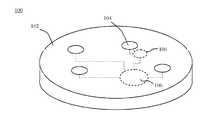
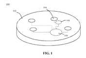
- FIG. 1is a perspective view schematic diagram illustrating a wafer having plugs for sensing devices according to an embodiment of the present invention.
- FIG. 2Ais a cross-sectional view of a sensing device according to an embodiment of the present invention.
- FIG. 2Bis a cross-sectional view of a sensing device according to an alternative embodiment of the present invention.
- FIG. 2Cis an equivalent electrical diagram of the sensing devices shown in FIGS. 2A-2B .
- FIG. 3is a top view of a sensing device according to an embodiment of the present invention.
- FIG. 4Ais a perspective view illustrating measurement of current across the surface of a plasma measurement device according to an embodiment of the present invention.
- FIG. 4Bis a combined cross-section and electrical schematic diagram of an equivalent circuit of the device shown in FIG. 4A .
- FIG. 4Cis an equivalent electrical circuit diagram of the device shown in FIG. 4B .
- a plasma sensing devicemay include sensors and electronics, embedded in the surface of a wafer substrate and directly visible to the plasma sheath.
- the surface of the wafer substrate and portion of the sensing device that is exposed to the plasmacan both be made of a material that is conventionally processed by the type of plasma that the device is designed to sense.
- a shunt impedance for one or more of the sensorscan be formed by a “slug” of material that is substantially the same as the material the wafer substrate and that is also directly visible to the plasma sheath.
- the term “substantially the same material”means that the one material is chemically similar if not physically identical to another material.
- the substrate and slug materialscan be substantially the same if the wafer substrate and slug are both made of single crystal silicon but with different crystalline orientations.
- the substrate and slug materialscan be substantially the same if the substrate is made of single crystal silicon and the slug is made of polycrystalline silicon.
- the term “substantially the same”also encompasses slight variations in the chemical composition the two materials, e.g., due to different but otherwise acceptable levels of impurities.
- Forming the shunt impedance in this mannerprovides a durable and non contaminating surface for the plasma and can also provide a DC connection to the surface of the substrate. Hence, surface DC potential may be measured.
- This structurecan give valuable information such as surface charge, self-bias, load-line characteristics or I-V characteristics is a DC bias is simultaneously imposed upon the sensor.
- FIG. 1is a perspective view of a sensing device 100 that includes a substrate 102 several slugs 104 as collectors for sensors.
- the substrate 102 and slugs 104can be made of the same material.
- the substrate 102 and slugs 104can both be made of silicon, or any other conductive or semiconductor material that is compatible with the processing conditions in the processing environment in which the device 100 is intended to operate.
- the substratemay include a silicon wafer with a diameter of between 100 mm and 450 mm.
- the sensing device 100may have an overall thickness of 0.3 mm to 10 mm
- the substrate 102 and slugs 104can provide a durable and non contaminating surface presented to the plasma.
- the substrate and a collector pad that is part of a sensormay be made of silicon so that the plasma “sees” a silicon surface.
- a plasma-compatible polymer coatingsuch as photoresist, can cover the surface of the wafer substrate.
- Many plasma process chambersare designed to process substrates that are covered with photoresist.
- the presence of photoresist on the surface of the substrate 102 and slugs 104poses no additional contamination hazard beyond those already taken into account in the design of the plasma process diagnosed by the device 100 and the chamber in which such a plasma process takes place.
- Contamination of a plasma chamber resulting from exposure of the surface of the substrate 102 and slugs 104 to the plasmamay be rectified by whatever conventional process is used following normal treatment of production substrates in the chamber. For example, after using the device 100 to diagnose a plasma in a chamber used to etch a silicon substrate covered with a patterned photoresist, the chamber may be cleaned by a conventional process normally used to clean such a chamber after such plasma etching.
- the slugs 104may be electrically coupled to sensor electronics 106 located beneath the surface of the substrate 102 . There may be more than one sensor electronics 106 below the surface of the substrate 102 for the purpose of processing the sensor signals.
- the slugsmay serve as collector pads for sensing a flux of electrons or ions or energetic radiation from a plasma.
- the substrate 102 and slugs 104may provide a DC connection from sensor electronics to the surface. Such a configuration can be used measure surface DC potential. Such a structure can also be used to obtain valuable information such as surface charge and self-bias.
- AC signal detectionmay be performed by a temperature compensated, DC biased high-frequency, diode bridge circuit. This method can eliminate the disadvantages of poor linearity and low power levels, frequency effects as well as temperature drift associated with prior art methods.
- the electronics 106may apply an excitation voltage at one sensor slug 104 and measure a signal at one or more different slugs to measure the plasma impedance.
- FIGS. 2A-2Bare cross-sectional views illustrating different implementations of sensing devices 200 A and 200 B.
- the sensing devices 200 A and 200 Bcan be used to measure electrical parameters such as self bias voltage, saturation current, charge and polymer build up in process chamber with process chemistry and under high plasma power over a wide range of RF and Microwave frequencies.
- the sensing device 200 Aincludes a first and second layers 202 and 204 respectively separated by an insulating layer 212 , which can be an oxide or other dielectric layer.
- the first layer 202can be made from the same material as a production wafer that is normally processed by the type of plasma the device 200 A is designed to sense.
- a cavity 216can be formed at the surface of the first layer 202 .
- a plug made of the same material as the first layer 202 sensorcan be positioned in the cavity 216 with the top surface of the plug 206 coplanar with the top surface of the first layer 202 .
- the underside of the plug 206can have a metallic coating 222 that is suitable for making an ohmic contact connection.
- the metallic coatingcan be diffused into the silicon and thus does not create a diode junction to the silicon.
- suitable materials for the metallic coating 222include platinum and palladium. If wire bonding is performed, aluminum can also be used. Therefore, the top surface of the device 200 can be made planar and have a profile substantially the same as that of a standard production substrate processed in the type of chamber that the device 200 A is designed for.
- a dielectric layer 220e.g., polyimide
- the dielectric layer 220can also form a shunt capacitance that can be used to measure an RF current which may be impinging on the sensor surface formed by plug 206 .
- the plug 206can be exposed to plasma and act as a signal collector by collecting a raw flux, e.g., charge (in the form of electrons or ions), from the plasma that can be detected as a raw signal, e.g., in the form of a current or voltage.
- a raw fluxe.g., charge (in the form of electrons or ions)
- the plug 206may be subject to radiation from the plasma in the form of energetic photons.
- the plug 206may be made of a semiconductor material having electrical properties that change upon exposure to such photons.
- the plug 206can be coupled to suitable sensor electronics 205 .
- the combination of a signal collector, such as the plug 206 , and sensor electronics 205is sometimes referred to herein as a sensor. Depending on the nature of the electronics, the sensor may be used to detect AC or DC signals.
- suitable sensor electronics 205include signal conditioning electronics and signal processing electronics.
- the electronicsmay include a power source, such as a battery, which may be used to apply a bias voltage to the plug 206 .
- signal conditioningincludes, but is not limited to, filtering, noise rejection, or amplification of the raw signal to make it more suitable for analysis.
- signal conditioning componentsinclude, but are not limited to, rectifiers, oscillators, or amplifiers.
- Signal processingrefers to analysis of a signal, e.g., using analog or digital circuitry. Signal processing may include, but is not limited to, analog-to-digital conversion, arithmetic and/or logical operations, Fourier transforms or other mathematical transforms, spectral analysis, and the like.
- signal processing componentsinclude, but are not limited to a microprocessor or an application-specific integrated circuit (ASIC).
- the electronics 205could include data acquisition (DAQ) electronics that produce a DC signal that is coupled to processing electronics.
- DAQdata acquisition
- the plug 206may be electrically connected to the electronics 205 , e.g., by circuitry, which may be embedded in the second silicon layer 204 or in the insulating layer 212 , e.g., in the form of a flex circuit 208 .
- the componentse.g., transistors, resistors, capacitors, logic devices, etc, that make up the electronics 205 can be connected by conductive (e.g., copper) traces patterned onto a polyimide flexible substrate.
- the electronic components that make up the sensor electronics 205 and associated circuitsmay be formed directly on the surface of the second layer 204 or the insulating layer 212 , e.g., using standard semiconductor processing techniques.
- the electronics 205may be electrically connected to the first layer 202 e.g., by an ohmic contact 214 coupled to the flex circuit 208 .
- An ohmic contact 214may also be formed between the first layer 202 and the second layer 204 .
- the ohmic contact 214can provide an electrical connection to the substrate 204 and 206 , e.g., by means of a suitable metallization 222 as described above.
- the ohmic contact 214may be expanded to essentially create a contact that would cover most of the available surface area of silicon layers 202 and 204 .
- multiple slugs 206may be used to provide multiple collectors that may be coupled to appropriate sensor electronics.
- the collectors and sensor electronicsmay be configured in many different ways to measure plasma parameters.
- pairs of collectors and corresponding sensor electronicsmay be configured to operate as dual differential Langmuir probes.
- the sensor electronicscan apply a bias voltage between two collectors and measure currents to the two collectors.
- ion saturation current and electron temperaturemay be determined from an I-V curve.
- triple differential Langmuir probe operationis possible or a differential Langmuir probe operated in a time division configuration.
- a triple differential probe with appropriate circuitrycan provide a response with minimal processing.
- two collectorsmay be biased positive and negative with a fixed voltage (V + -V ⁇ ) between them while a voltage on a third collector is allowed to float to the plasma floating potential V B .
- the bias voltageis sufficiently large compared to the electron temperature (i.e., e(V + ⁇ V ⁇ )>>k B T e , where e is the charge on the electron and k B is Boltzmann's constant)
- the negative biased collectorcan be expected to draw the ion saturation current, which, like the floating potential V fl , can be directly measured.
- the biased collector configurationis floating, the current to the positive-biased collector is approximately equal in magnitude to the ion saturation current drawn by the negative-biased collector and the floating collector can be expected to effectively draw no current.
- Triple probescan be symmetrically, asymmetrically or highly asymmetrically depending on the region the probe is expected to operate under.
- Triple probeshave the advantage of simple biasing electronics (no sweeping of the bias voltage is required), simple data analysis, excellent time resolution, and insensitivity to potential fluctuations (whether imposed by an RF source or inherent fluctuations). The disadvantage is that they require three probe areas which may not be possible to implement in all cases.
- bias voltage conditionsmay be set and used to derive an electron temperature T e and ion density n i with a dual Langmuir probe.
- the Ion Saturation current, I satmay also be similarly estimated. The result is very similar to the triple probe but using only two probe areas.
- Sensing device 200 B shown in FIG. 2Bis similar to the sensing device 200 described in FIG. 2A , except that the silicon plug 206 is positioned on the insulating layer 212 like the first layer 202 .
- the plugmay be formed from a silicon-on-insulator (SOI) wafer in which the insulator is disposed between two layers of silicon. By selectively etching one of the two silicon layers the plug 206 may be electrically separated from a remaining portion of that layer. The plug may be further insulated from the silicon layer by additional insulating material 217 .
- SOIsilicon-on-insulator
- the surface of the plug 206can be made almost perfectly flush with the surface of the rest of the first layer 202 . Furthermore, the first layer 202 and the plug 206 can be assured to have almost identical material properties.
- the first layer 202 and second layer 204may be made sufficiently electrically conducting (e.g., by suitable doping) so that they form a Faraday cage that is suitable for protecting the electronics 204 from electromagnetic interference during operation within a Plasma procession environment.
- FIG. 2Cis an electrical schematic diagram of an equivalent circuit of the sensing devices illustrated in FIGS. 2A-2B .
- a polymer layer 218may build up on the surface of the first layer 202 as a result of a polymerization reaction that takes place in the plasma chamber. Such polymerization is a fairly common occurrence in many types of plasma processing.
- the polymerization layer 218can affect the measurements made with the devices 200 A, 200 B.
- the surface of a collector portion, e.g., plug 206can be modified, e.g., by etching a three-dimensional pattern into the surface or by deliberately coating it with one or more materials 219 such as a photoresist and/or metal to modify the interaction between the collector and a plasma.
- the material 219can be deposited or otherwise formed in pattern, e.g., a grid or series of stripes. The material 219 can be different from the material that makes up the bulk of the plug 206 .
- the polymer layer 218can act as a variable capacitor C 1 .
- a measuring capacitor C 2may be formed in series with the variable capacitor C 1 due to the polymer layer with the silicon plug 206 as the upper plate and the electronics, first and second silicon layers 202 and 204 and the ohmic contacts 214 forming the lower plate of the capacitor.
- the polyimide layer 220can act as an insulating material between two plates of the measuring capacitor C 2 .
- the capacitor C 2can be connected to a power source, e.g., a battery, B. If a switch SW is added across the plates of the measuring capacitor C 2 , a rate of the electron built up on the surface of the substrate could be measured by shorting the plates of the measuring capacitor C 2 by closing the switch and then measuring the voltage change when the switch is opened.
- FIG. 3is a top view of a sensing device 300 according to an embodiment of the present invention.
- the sensing device 300includes a substrate 302 with several sensors 304 , which may be similar to the sensing devices 200 and 201 as described in FIGS. 2A-2B .
- each sensor 304may include a collector 306 that is formed from the same material as the surface of the substrate 302 .
- a surface of the collectormay be flush with the surface of the substrate 302 .
- the collector 306may be coupled through sensor 304 to local sensor electronics 305 which may be embedded into the substrate 302 .
- the collector 306may include such features as patterned film-stacks, micro-machined surface features or simply a metal film such as a layer of aluminum.
- the sensing device 300may include a centralized processing and/or communication electronics unit 308 that is coupled to each of the sensors 304 and collector 306 if any.
- the centralized electronics 308can provide centralized component for transmitting and storing data from the sensors 304 out of device 300 to a remote receiver.
- the electronicscan also provide a centralized component for receiving data from an external transmitter and relaying such data to one or more selected individual sensors 304 .
- the electronics 300may include a wireless or wired transceiver unit that converts the data into signals that can be transmitted wirelessly, e.g., by electromagnetic induction or radiation.
- the electronics 308may transmit the signals over a medium, such as a signal cable or fiber optic link.
- suitable sensor electronics 305include signal conditioning electronics and signal processing electronics.
- the electronicsmay include a power source, such as a battery, which may be used to apply a bias voltage to the sensor 304 and collector 306 .
- signal conditioningincludes, but is not limited to, filtering, noise rejection, or amplification of the raw signal to make it more suitable for analysis.
- signal conditioning componentsinclude, but are not limited to, rectifiers, oscillators, or amplifiers.
- Signal processingrefers to analysis of a signal, e.g., using analog or digital circuitry. Signal processing may include, but is not limited to, analog-to-digital conversion, arithmetic and/or logical operations, Fourier transforms or other mathematical transforms, spectral analysis, and the like.
- signal processing componentsinclude, but are not limited to a microprocessor or an application-specific integrated circuit (ASIC).
- the electronics 305could include a localized processor unit that is specific to the sensor 304 with which it is associated. By using a localized processor unit at each sensor 304 , part of the burden of processing the raw signals from the sensor 304 and collectors 306 may be distributed. In this way, the processing burden may be made to scale with the number of sensors on the device 300 without having to add processing capacity to the centralized electronics 308 .
- the sensor electronics 305could perform certain digital signal filtering functions on the raw data and then transmit the resulting filtered data to the centralized electronics. This frees up processing resources on the centralized electronics for collating the filtered data from the different sensors 304 .
- a sensor devicemay include a collector may be formed from the same material as a production substrate.
- the collector padcomprises an entire continuous surface of the sensor device.
- a single continuous surface of silicon substratemay be used as a collector pad.
- FIG. 4Ais a schematic perspective view illustrating a plasma sensing device 400 according to an alternative embodiment of the invention.
- a collectoris made from a substrate 402 that is made of resistive material that the same as or similar to the material used in production substrates that are subject to plasma 401 in a process chamber.
- the substrate 402may have a planar top surface that has substantially the same profile as a production substrate that is processed in the process chamber. If charge builds up non-uniformly on the surface of the substrate 401 , a sheet current I s may flow across the surface of the substrate 401 . As shown in FIG. 4A , a voltage may be measured between different locations A and B on the surface of the substrate 401 .
- the sheet current I scan be used as measure of the charge imbalance across the substrate surface. Specifically, the voltage between points A and B may be determined from the current, which depends on sheet resistivity of the substrate material 401 and the charge imbalance between the two points.
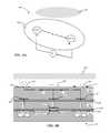
- FIG. 4Bis a combination equivalent electrical circuit schematic diagram and cross-sectional view of the sensing device 400 .
- the sensing device 400generally includes an upper semiconductor substrate 402 and a lower semiconductor substrate 404 .
- an intermediate semiconductor substrate 416may be sandwiched between the upper and lower substrates.
- the substrates 402 , 404 , 416are sometimes referred to below simply as the upper, middle, and lower substrates.
- upper substrate 402may be a first silicon layer 402 doped P ⁇ to make it resistive
- the bottom substrate 404may be a second silicon layer doped P+ to make it conductive.
- An insulating layer 428is sandwiched between the upper and lower substrates 402 and 404 . In the example shown in FIG.
- the insulating layeris more specifically sandwiched between the upper substrate 402 and the intermediate substrate 416 .
- the insulating layer 428may be relatively, thick, e.g., 25 microns or more in thickness.
- oxidemay be implanted into a silicon wafer.
- oxidemay be grown on the surface of a silicon wafer and polycrystalline silicon (polysilicon) may be grown or deposited on the oxide.
- a polymer layermay be laminated between two silicon wafers.
- an insulating layer 430may be formed between substrates 404 and 416 .
- Suitable electronics 418may be positioned in cavities formed in the lower substrate 404 . Each electronics unit may be electrically coupled to a corresponding sensor contact 403 , by a corresponding pattered metallization or a pattered flexible circuit 408 formed on, or inlaid into, the lower substrate 404 .
- the electronicscan be configured to measure direct current (DC) or alternating current (AC) electrical quantities such as voltage, current, charge, capacitance, and the like at the sensor locations 403 .
- the electronics 418may excite one or more sensor contacts 403 and/or a reference contact 405 with DC levels or AC waveforms and simultaneously measure AC and DC parameters at other sensor contact locations 403 and/or reference contact 405 to determine various plasma parameters.
- the electronics 418may apply an excitation voltage at one sensor contact 403 and measure a signal at one or more different sensor contacts and/or the reference contact 405 to measure the plasma impedance.
- the excitation voltagemay be applied to the reference contact 405 and signals may be measured at the sensor contacts 403 .
- the collector portions of the sensorscan be embedded in a substrate by forming them as integral parts of the upper semiconductor layer 402 .
- one or more sensor contactscan be formed by depositing a suitable conductive material such as platinum, palladium or aluminum in the areas of the sensor contacts 403 and reference contact 405 , in locations on an underside of the upper semiconductor layer 402 where a sensor is desired. The can be diffused into the upper semiconductor layer 402 thus creating a ohmic connection. Since the vertical dimension of the upper semiconductor layer 402 is much smaller that the horizontal dimension, the effect is that the metallic sensor contacts 403 at the bottom of the upper layer 402 is mirrored onto the top surface as a virtual sensor 420 .
- the effect of the central reference contact 405is mirrored as a virtual sensor 422 .
- Any voltage present at the top surfacewould be translated to the bottom surface and there for can be sensed and driven by appropriate electronics 418 .
- the reference contact 405 at a center positionmay be connected to the middle substrate 416 via a electronic switch in the electronics module 418 .
- Such ohmic contact to substrate 416can effectively provide for a DC reference potential of the middle and lower substrates 416 and 404 .
- This DC referencecan be important, e.g., when measuring DC voltages with the electronics 418 , but can be turned of when measuring AC voltages.
- one or more portions of the surface of one or more collector portionscan be modified, e.g., by etching a three-dimensional pattern into the surface or by deliberately coating them with a material 419 such as a photoresist and/or metal to modify the interaction between the collector and a plasma.
- the material 419can be deposited or otherwise formed in pattern, e.g., a grid or series of stripes. The material can be different from the material that makes up the bulk of the upper layer 402 .
- the electronics 418can sense sheet currents I e flowing through the upper substrate 402 between the sensor contacts 403 and a reference contact 405 at a center location thereby providing a measure of the self-bias and charge build-up on the surface of the upper layer 402 . Voltage differences can be measured due to the sheet resistance of upper layer 402 and the sheet currents I e flowing between different sensor contacts 403 and/or between the sensor contacts 403 and the reference contact 405 .
- the sheet resistance of the substrateis represented by resistors designated R sub .
- the charge imbalance over the surface of the upper silicon layer 402can be measured in real time.
- the voltage or charge measurementscan be converted to digital data and stored at a central electronics unit (not shown) for later transmission to an external receiver without having to remove the device 400 from the plasma chamber.
- the middle and lower substrates 416 and 404may also act as a Faraday cage for shielding of the electronics 418 and the associated metallization 408 .
- the middle substrate 416 and the lower 404can be ohmically connected to each other through contacts 426 , and 413 , which may be in the form of metallization regions created in a manner similar to that described above, and/or the ohmic contact 432 .
- the upper substrate 402 together with insulating layer 428 and base substrate 416can act as a distributed capacitor. This capacitance can serve as a test load to sense an RF current by the RF voltage generated at each sensing point. The amplitudes of such voltages may be rectified and measured by the electronics 418 .
- the local part of the distributed capacitanceis equivalent to the capacitor C 2 shown in FIG. 2C .
- the equivalent capacitances between the sensor contacts 403are indicated as C and C′ in FIG. 4C .
- the equivalent capacitance between the reference contact 405 and the plasmais indicated as C′′ in FIG. 4C .
- the DC part of the signal, as measured by the electronics 418 , at the sensor contact 403is related to the charge distribution.
- the sensor contact 403 and reference contact 405may also be excited by an applied AC or DC voltage for measurement of parameters such as ion saturation current, electron temperature and plasma impedance.
- a collector area 424 constructed with pattered film stackscan be placed upon the first surface of substrate 402 to modify the electrical response of the substrate 402 to the plasma.
- Embodiments of the present inventionprovide a tool for measurement of ion and electron characteristics of a plasma and, optionally, for measurement of surface charging in a wafer production system.
- the ability to measure these quantities in a wafer production systemcan provide additional insight to plasma processing surface parameters.
- surface related topologymay radically alter the behavior of the sensing locations and this phenomenon may be taken advantage of to measure such parameters such as polymer re-deposition, ion angles and charge damage with higher sensitivity and a wider dynamic range.
- Embodiments of the present inventioncan help more easily identify key elements that affect plasma chamber performance and subsequently adjust the relevant parameter to optimize performance.
Landscapes
- Engineering & Computer Science (AREA)
- Physics & Mathematics (AREA)
- Plasma & Fusion (AREA)
- Chemical & Material Sciences (AREA)
- Analytical Chemistry (AREA)
- General Physics & Mathematics (AREA)
- Manufacturing & Machinery (AREA)
- Power Engineering (AREA)
- Microelectronics & Electronic Packaging (AREA)
- Computer Hardware Design (AREA)
- Condensed Matter Physics & Semiconductors (AREA)
- Automation & Control Theory (AREA)
- Chemical Kinetics & Catalysis (AREA)
- Pathology (AREA)
- Electromagnetism (AREA)
- Spectroscopy & Molecular Physics (AREA)
- Immunology (AREA)
- General Health & Medical Sciences (AREA)
- Biochemistry (AREA)
- Life Sciences & Earth Sciences (AREA)
- Health & Medical Sciences (AREA)
- Electrochemistry (AREA)
- Drying Of Semiconductors (AREA)
- Plasma Technology (AREA)
- Testing Or Measuring Of Semiconductors Or The Like (AREA)
Abstract
Description
- This Application is a divisional of commonly-assigned U.S. patent application Ser. No. 14/505,289, filed Oct. 2, 2014, the entire contents of which are incorporated herein by reference.
- Application Ser. No. 14/505,289 is a divisional of commonly-assigned U.S. patent application Ser. No. 12/691,695, filed Jan. 21, 2010, the entire contents of which are incorporated herein by reference.
- This invention relates generally to plasma processing systems, and more particularly to apparatus for making in-situ measurements of plasma properties in plasma processing systems.
- Plasma processes are frequently used to modify or treat the surfaces of workpieces such as semiconductor wafers, flat-panel display substrates, and lithography masks. Conditions within a plasma process are designed to produce a complex mixture of ions, reactive chemical species (free radicals), and energetic neutral species. The interaction of these materials then produces the desired effect on the surfaces of workpieces. For example, plasma processes are used to etch materials from the surfaces of semiconductor wafers so as to form complex electrical elements and circuits. The conditions within the plasma process are carefully controlled to produce the desired etch directionality and selectivity.
- The surface modifications produced by a specific plasma are sensitive to a number of basic parameters within the plasma. These parameters include such variables as: chemical concentrations (partial pressures), temperatures (both surface and gas phase), and electrical parameters (ion fluxes, ion energy distribution functions). A number of these parameters (e.g. gas concentrations and pressure) can generally be easily controlled using external actuators such as Mass Flow Controllers (MFCs) and servo driven throttle valves. Other important parameters (e.g. temperatures and free radical concentrations) can often be observed or measured via sensor systems (e.g. thermocouples and Optical Emission Spectrometers (OES)) installed on the process tool. A last set of important parameters such as ion fluxes and ion energies are more difficult to either directly control or monitor.
- US publication No. 2005-0151544 discloses a plasma processing system with diagnostic apparatus for making in-situ measurements of plasma properties. The diagnostic apparatus generally comprises a non-invasive sensor array disposed within a plasma processing chamber, an electrical circuit for stimulating the sensors, and means for recording and communicating sensor measurements for monitoring or control of the plasma process. In one form, the sensors are dynamically pulsed dual floating Langmuir probes that measure I-V characteristic, displacement RF current into or through the wafer and self-bias due to electrons piling up on the surface, which can be used to determined the charge on the wafer.
- Wafer charges are formed due to different flux rates for ions and electrons (due to their very different masses). Wafer charging can lead to damage to the devices. One type of tool that is conventionally used for characterizing wafer charging during wafer processing in ion-based and plasma-based IC processing equipment includes EEPROM-based peak potential sensors and current sensors to characterize the I-V relationship of charging transients. The gate of the transistors is coupled to the antenna structures on the wafer. The device measures the cumulative charge, not charge as a function of time. Furthermore, the wafer has to be taken out of the plasma chamber to read the charge measurement.
- US publication No. 2006-0249729 discloses a sensor wafer that uses a triple capacitor stack to measure apparent alternating current (AC) at the surface of the wafer. This rectification (detection) device has a minimum bias requirement and a strong frequency dependency on the range of interest. The measurement is purely AC and the center capacitor, formed by a polyimide substrate is the shunt impedance that generates the AC potential to be measured. The sensor responds in a confounded way to a number of electrical parameters in the plasma chamber and is unable to relate specifically to any one parameter. This makes it difficult to find the right “knobs” to tune the chamber when problems are encountered.
- In addition, many prior art sensor wafers include a module atop of the wafer that houses electronics for the sensor array. This module can cause severe disturbance in the plasma or can be a point of discharge damages and can also be a source for contamination.
- Another problem with prior art sensor wafers is that sensor pads in the array and electrical connections between these pads and associated electronics are often made of metal traces, e.g., Aluminum, that is deposited on the surface of the wafer. Exposure to plasma, e.g., Argon plasma, eventually erodes aluminum traces on the surface of the wafer. In some sensor wafers, entire surface of the wafer is covered by polyimide to protect the traces and sensor pads. However, the polyimide coating can have a very short life time in certain plasma environments and may also be a source of contamination. In addition, the use of certain metals, such as copper, is strongly avoided in many process steps.
- It is within this context that embodiments of the present invention arise.
- Objects and advantages of embodiments of the invention will become apparent upon reading the following detailed description and upon reference to the accompanying drawings in which:
FIG. 1 is a perspective view schematic diagram illustrating a wafer having plugs for sensing devices according to an embodiment of the present invention.FIG. 2A is a cross-sectional view of a sensing device according to an embodiment of the present invention.FIG. 2B is a cross-sectional view of a sensing device according to an alternative embodiment of the present invention.FIG. 2C is an equivalent electrical diagram of the sensing devices shown inFIGS. 2A-2B .FIG. 3 is a top view of a sensing device according to an embodiment of the present invention.FIG. 4A is a perspective view illustrating measurement of current across the surface of a plasma measurement device according to an embodiment of the present invention.FIG. 4B is a combined cross-section and electrical schematic diagram of an equivalent circuit of the device shown inFIG. 4A .FIG. 4C is an equivalent electrical circuit diagram of the device shown inFIG. 4B .- Although the following detailed description contains many specific details for the purposes of illustration, anyone of ordinary skill in the art will appreciate that many variations and alterations to the following details are within the scope of the invention. Accordingly, the exemplary embodiments of the invention described below are set forth without any loss of generality to, and without imposing limitations upon, the claimed invention.
- According to one embodiment of the present invention, a plasma sensing device may include sensors and electronics, embedded in the surface of a wafer substrate and directly visible to the plasma sheath. The surface of the wafer substrate and portion of the sensing device that is exposed to the plasma can both be made of a material that is conventionally processed by the type of plasma that the device is designed to sense. By way of example, in some embodiments, a shunt impedance for one or more of the sensors can be formed by a “slug” of material that is substantially the same as the material the wafer substrate and that is also directly visible to the plasma sheath. As used herein, the term “substantially the same material” means that the one material is chemically similar if not physically identical to another material. For example, the substrate and slug materials can be substantially the same if the wafer substrate and slug are both made of single crystal silicon but with different crystalline orientations. Alternatively, the substrate and slug materials can be substantially the same if the substrate is made of single crystal silicon and the slug is made of polycrystalline silicon. The term “substantially the same” also encompasses slight variations in the chemical composition the two materials, e.g., due to different but otherwise acceptable levels of impurities.
- Forming the shunt impedance in this manner provides a durable and non contaminating surface for the plasma and can also provide a DC connection to the surface of the substrate. Hence, surface DC potential may be measured. This structure can give valuable information such as surface charge, self-bias, load-line characteristics or I-V characteristics is a DC bias is simultaneously imposed upon the sensor.
FIG. 1 is a perspective view of asensing device 100 that includes asubstrate 102several slugs 104 as collectors for sensors. Thesubstrate 102 andslugs 104 can be made of the same material. By way of example, and not by way of limitation, thesubstrate 102 andslugs 104 can both be made of silicon, or any other conductive or semiconductor material that is compatible with the processing conditions in the processing environment in which thedevice 100 is intended to operate. By way of example, and not by way of limitation, the substrate may include a silicon wafer with a diameter of between 100 mm and 450 mm. Thesensing device 100 may have an overall thickness of 0.3 mm to 10 mm- The
substrate 102 andslugs 104 can provide a durable and non contaminating surface presented to the plasma. For example, if the plasma diagnosed by the sensing device is conventionally used for processing, e.g., etching of or deposition on silicon wafers, the substrate and a collector pad that is part of a sensor may be made of silicon so that the plasma “sees” a silicon surface. In some implementations, if it is desired to present a dielectric surface to the plasma, a plasma-compatible polymer coating, such as photoresist, can cover the surface of the wafer substrate. Many plasma process chambers are designed to process substrates that are covered with photoresist. Consequently, the presence of photoresist on the surface of thesubstrate 102 andslugs 104 poses no additional contamination hazard beyond those already taken into account in the design of the plasma process diagnosed by thedevice 100 and the chamber in which such a plasma process takes place. Contamination of a plasma chamber resulting from exposure of the surface of thesubstrate 102 andslugs 104 to the plasma may be rectified by whatever conventional process is used following normal treatment of production substrates in the chamber. For example, after using thedevice 100 to diagnose a plasma in a chamber used to etch a silicon substrate covered with a patterned photoresist, the chamber may be cleaned by a conventional process normally used to clean such a chamber after such plasma etching. - The
slugs 104 may be electrically coupled tosensor electronics 106 located beneath the surface of thesubstrate 102. There may be more than onesensor electronics 106 below the surface of thesubstrate 102 for the purpose of processing the sensor signals. By way of example, the slugs may serve as collector pads for sensing a flux of electrons or ions or energetic radiation from a plasma. In some implementations, thesubstrate 102 andslugs 104 may provide a DC connection from sensor electronics to the surface. Such a configuration can be used measure surface DC potential. Such a structure can also be used to obtain valuable information such as surface charge and self-bias. In some implementations, AC signal detection may be performed by a temperature compensated, DC biased high-frequency, diode bridge circuit. This method can eliminate the disadvantages of poor linearity and low power levels, frequency effects as well as temperature drift associated with prior art methods. - In some embodiments, the
electronics 106 may apply an excitation voltage at onesensor slug 104 and measure a signal at one or more different slugs to measure the plasma impedance. - According to some embodiments of the present invention, active circuitry and a power-source may be embedded into and/or in-between layers of a device like that shown in
FIG. 1 , thereby effectively forming a Faraday cage around such components. By way of example, and not by way of limitation,FIGS. 2A-2B are cross-sectional views illustrating different implementations ofsensing devices sensing devices - As shown in
FIG. 2A , thesensing device 200A includes a first andsecond layers layer 212, which can be an oxide or other dielectric layer. Thefirst layer 202 can be made from the same material as a production wafer that is normally processed by the type of plasma thedevice 200A is designed to sense. In thedevice 200A acavity 216 can be formed at the surface of thefirst layer 202. A plug made of the same material as thefirst layer 202 sensor can be positioned in thecavity 216 with the top surface of theplug 206 coplanar with the top surface of thefirst layer 202. The underside of theplug 206 can have ametallic coating 222 that is suitable for making an ohmic contact connection. By way of example, the metallic coating can be diffused into the silicon and thus does not create a diode junction to the silicon. Examples of suitable materials for themetallic coating 222 include platinum and palladium. If wire bonding is performed, aluminum can also be used. Therefore, the top surface of the device200 can be made planar and have a profile substantially the same as that of a standard production substrate processed in the type of chamber that thedevice 200A is designed for. A dielectric layer220 (e.g., polyimide) can be deposited between thesilicon plug 206 and thefirst layer 202 to provide electrical isolation. Thedielectric layer 220 can also form a shunt capacitance that can be used to measure an RF current which may be impinging on the sensor surface formed byplug 206. - The
plug 206 can be exposed to plasma and act as a signal collector by collecting a raw flux, e.g., charge (in the form of electrons or ions), from the plasma that can be detected as a raw signal, e.g., in the form of a current or voltage. Alternatively, theplug 206 may be subject to radiation from the plasma in the form of energetic photons. To detect such photons, theplug 206 may be made of a semiconductor material having electrical properties that change upon exposure to such photons. Theplug 206 can be coupled tosuitable sensor electronics 205. The combination of a signal collector, such as theplug 206, andsensor electronics 205 is sometimes referred to herein as a sensor. Depending on the nature of the electronics, the sensor may be used to detect AC or DC signals. - Examples of
suitable sensor electronics 205 include signal conditioning electronics and signal processing electronics. In addition, the electronics may include a power source, such as a battery, which may be used to apply a bias voltage to theplug 206. As used herein, signal conditioning includes, but is not limited to, filtering, noise rejection, or amplification of the raw signal to make it more suitable for analysis. Examples of signal conditioning components include, but are not limited to, rectifiers, oscillators, or amplifiers. Signal processing refers to analysis of a signal, e.g., using analog or digital circuitry. Signal processing may include, but is not limited to, analog-to-digital conversion, arithmetic and/or logical operations, Fourier transforms or other mathematical transforms, spectral analysis, and the like. Examples of signal processing components include, but are not limited to a microprocessor or an application-specific integrated circuit (ASIC). By way of example, and not by way of limitation, theelectronics 205 could include data acquisition (DAQ) electronics that produce a DC signal that is coupled to processing electronics. - The
plug 206 may be electrically connected to theelectronics 205, e.g., by circuitry, which may be embedded in thesecond silicon layer 204 or in the insulatinglayer 212, e.g., in the form of aflex circuit 208. In such a case, the components (e.g., transistors, resistors, capacitors, logic devices, etc, that make up theelectronics 205 can be connected by conductive (e.g., copper) traces patterned onto a polyimide flexible substrate. Alternatively the electronic components that make up thesensor electronics 205 and associated circuits may be formed directly on the surface of thesecond layer 204 or the insulatinglayer 212, e.g., using standard semiconductor processing techniques. Theelectronics 205 may be electrically connected to thefirst layer 202 e.g., by anohmic contact 214 coupled to theflex circuit 208. Anohmic contact 214 may also be formed between thefirst layer 202 and thesecond layer 204. Theohmic contact 214 can provide an electrical connection to thesubstrate suitable metallization 222 as described above. Furthermore, theohmic contact 214, may be expanded to essentially create a contact that would cover most of the available surface area ofsilicon layers - It is noted that
multiple slugs 206 may be used to provide multiple collectors that may be coupled to appropriate sensor electronics. The collectors and sensor electronics may be configured in many different ways to measure plasma parameters. For example, with appropriate electronics and additional circuits, pairs of collectors and corresponding sensor electronics may be configured to operate as dual differential Langmuir probes. In such a configuration, the sensor electronics can apply a bias voltage between two collectors and measure currents to the two collectors. By varying the bias voltage, ion saturation current and electron temperature may be determined from an I-V curve. Furthermore, by simplification of the control circuitry, triple differential Langmuir probe operation is possible or a differential Langmuir probe operated in a time division configuration. - A triple differential probe with appropriate circuitry can provide a response with minimal processing. In a triple probe configuration, two collectors may be biased positive and negative with a fixed voltage (V+-V−) between them while a voltage on a third collector is allowed to float to the plasma floating potential VB. If the bias voltage is sufficiently large compared to the electron temperature (i.e., e(V+−V−)>>kBTe, where e is the charge on the electron and kBis Boltzmann's constant) the negative biased collector can be expected to draw the ion saturation current, which, like the floating potential Vfl, can be directly measured. If the biased collector configuration is floating, the current to the positive-biased collector is approximately equal in magnitude to the ion saturation current drawn by the negative-biased collector and the floating collector can be expected to effectively draw no current.
- Under these conditions the electron temperature is approximately proportional to the measured voltages as follows:
(V+−Vfl)=ln 2(kBTe/e).- More sophisticated analysis of triple probe data can take into account such factors as incomplete saturation, non-saturation, unequal areas. Triple probes also can be symmetrically, asymmetrically or highly asymmetrically depending on the region the probe is expected to operate under. Triple probes have the advantage of simple biasing electronics (no sweeping of the bias voltage is required), simple data analysis, excellent time resolution, and insensitivity to potential fluctuations (whether imposed by an RF source or inherent fluctuations). The disadvantage is that they require three probe areas which may not be possible to implement in all cases.
- Alternatively, by time division multiplexing, four bias voltage conditions may be set and used to derive an electron temperature Teand ion density niwith a dual Langmuir probe. The Ion Saturation current, Isat, may also be similarly estimated. The result is very similar to the triple probe but using only two probe areas.
Sensing device 200B shown inFIG. 2B is similar to the sensing device200 described inFIG. 2A , except that thesilicon plug 206 is positioned on the insulatinglayer 212 like thefirst layer 202. By way of example, and not by way of limitation, the plug may be formed from a silicon-on-insulator (SOI) wafer in which the insulator is disposed between two layers of silicon. By selectively etching one of the two silicon layers theplug 206 may be electrically separated from a remaining portion of that layer. The plug may be further insulated from the silicon layer by additional insulatingmaterial 217. By forming theplug 206 from the same initial material as thefirst layer 202 the surface of theplug 206 can be made almost perfectly flush with the surface of the rest of thefirst layer 202. Furthermore, thefirst layer 202 and theplug 206 can be assured to have almost identical material properties.- It is noted that in the
devices first layer 202 andsecond layer 204 may be made sufficiently electrically conducting (e.g., by suitable doping) so that they form a Faraday cage that is suitable for protecting theelectronics 204 from electromagnetic interference during operation within a Plasma procession environment. FIG. 2C is an electrical schematic diagram of an equivalent circuit of the sensing devices illustrated inFIGS. 2A-2B . As indicated inFIGS. 2A-2B , apolymer layer 218 may build up on the surface of thefirst layer 202 as a result of a polymerization reaction that takes place in the plasma chamber. Such polymerization is a fairly common occurrence in many types of plasma processing. Thepolymerization layer 218 can affect the measurements made with thedevices - In some embodiments, the surface of a collector portion, e.g., plug206 can be modified, e.g., by etching a three-dimensional pattern into the surface or by deliberately coating it with one or
more materials 219 such as a photoresist and/or metal to modify the interaction between the collector and a plasma. By way of example, and not by way of limitation, thematerial 219 can be deposited or otherwise formed in pattern, e.g., a grid or series of stripes. Thematerial 219 can be different from the material that makes up the bulk of theplug 206. - Specifically, as shown in
FIG. 2C , thepolymer layer 218 can act as a variable capacitor C1. Referring simultaneously toFIG. 2A andFIG. 2C , a measuring capacitor C2may be formed in series with the variable capacitor C1due to the polymer layer with thesilicon plug 206 as the upper plate and the electronics, first and second silicon layers202 and204 and theohmic contacts 214 forming the lower plate of the capacitor. Thepolyimide layer 220 can act as an insulating material between two plates of the measuring capacitor C2. The capacitor C2can be connected to a power source, e.g., a battery, B. If a switch SW is added across the plates of the measuring capacitor C2, a rate of the electron built up on the surface of the substrate could be measured by shorting the plates of the measuring capacitor C2by closing the switch and then measuring the voltage change when the switch is opened. FIG. 3 is a top view of asensing device 300 according to an embodiment of the present invention. As shown inFIG. 3 , thesensing device 300 includes asubstrate 302 withseveral sensors 304, which may be similar to the sensing devices200 and201 as described inFIGS. 2A-2B . Specifically, eachsensor 304 may include acollector 306 that is formed from the same material as the surface of thesubstrate 302. A surface of the collector may be flush with the surface of thesubstrate 302. Thecollector 306 may be coupled throughsensor 304 tolocal sensor electronics 305 which may be embedded into thesubstrate 302. Thecollector 306 may include such features as patterned film-stacks, micro-machined surface features or simply a metal film such as a layer of aluminum. In addition, thesensing device 300 may include a centralized processing and/orcommunication electronics unit 308 that is coupled to each of thesensors 304 andcollector 306 if any. Thecentralized electronics 308 can provide centralized component for transmitting and storing data from thesensors 304 out ofdevice 300 to a remote receiver. The electronics can also provide a centralized component for receiving data from an external transmitter and relaying such data to one or more selectedindividual sensors 304. Theelectronics 300 may include a wireless or wired transceiver unit that converts the data into signals that can be transmitted wirelessly, e.g., by electromagnetic induction or radiation. Alternatively, theelectronics 308 may transmit the signals over a medium, such as a signal cable or fiber optic link.- Examples of
suitable sensor electronics 305 include signal conditioning electronics and signal processing electronics. In addition, the electronics may include a power source, such as a battery, which may be used to apply a bias voltage to thesensor 304 andcollector 306. As noted above, signal conditioning includes, but is not limited to, filtering, noise rejection, or amplification of the raw signal to make it more suitable for analysis. Examples of signal conditioning components include, but are not limited to, rectifiers, oscillators, or amplifiers. Signal processing refers to analysis of a signal, e.g., using analog or digital circuitry. Signal processing may include, but is not limited to, analog-to-digital conversion, arithmetic and/or logical operations, Fourier transforms or other mathematical transforms, spectral analysis, and the like. Examples of signal processing components include, but are not limited to a microprocessor or an application-specific integrated circuit (ASIC). - By way of example, and not by way of limitation, the
electronics 305 could include a localized processor unit that is specific to thesensor 304 with which it is associated. By using a localized processor unit at eachsensor 304, part of the burden of processing the raw signals from thesensor 304 andcollectors 306 may be distributed. In this way, the processing burden may be made to scale with the number of sensors on thedevice 300 without having to add processing capacity to thecentralized electronics 308. For example, in addition to rectification, amplification, and A/D conversion thesensor electronics 305 could perform certain digital signal filtering functions on the raw data and then transmit the resulting filtered data to the centralized electronics. This frees up processing resources on the centralized electronics for collating the filtered data from thedifferent sensors 304. - It is noted that embodiments of the present invention encompass many different configurations in which a sensor device may include a collector may be formed from the same material as a production substrate. These embodiments include versions in which the collector pad comprises an entire continuous surface of the sensor device. By way of example, and not by way of limitation, a single continuous surface of silicon substrate may be used as a collector pad. By measuring voltage differences between different locations on the surface of the substrate it is possible to determine differences in surface charge buildup.
FIG. 4A is a schematic perspective view illustrating aplasma sensing device 400 according to an alternative embodiment of the invention. In thedevice 400, a collector, is made from asubstrate 402 that is made of resistive material that the same as or similar to the material used in production substrates that are subject toplasma 401 in a process chamber. Thesubstrate 402 may have a planar top surface that has substantially the same profile as a production substrate that is processed in the process chamber. If charge builds up non-uniformly on the surface of thesubstrate 401, a sheet current Ismay flow across the surface of thesubstrate 401. As shown inFIG. 4A , a voltage may be measured between different locations A and B on the surface of thesubstrate 401. If the substrate material has a sufficiently large sheet resistance, the sheet current Iscan be used as measure of the charge imbalance across the substrate surface. Specifically, the voltage between points A and B may be determined from the current, which depends on sheet resistivity of thesubstrate material 401 and the charge imbalance between the two points.FIG. 4B is a combination equivalent electrical circuit schematic diagram and cross-sectional view of thesensing device 400. Thesensing device 400 generally includes anupper semiconductor substrate 402 and alower semiconductor substrate 404. In some embodiments, anintermediate semiconductor substrate 416 may be sandwiched between the upper and lower substrates. For convenience thesubstrates upper substrate 402 may be afirst silicon layer 402 doped P− to make it resistive, and thebottom substrate 404 may be a second silicon layer doped P+ to make it conductive. An insulatinglayer 428 is sandwiched between the upper andlower substrates FIG. 4B , the insulating layer is more specifically sandwiched between theupper substrate 402 and theintermediate substrate 416. The insulatinglayer 428 may be relatively, thick, e.g., 25 microns or more in thickness. There are a number of ways to form the insulatinglayer 428. For example, oxide may be implanted into a silicon wafer. Alternatively, oxide may be grown on the surface of a silicon wafer and polycrystalline silicon (polysilicon) may be grown or deposited on the oxide. In addition, a polymer layer may be laminated between two silicon wafers.- Similarly, an insulating
layer 430 may be formed betweensubstrates Suitable electronics 418 may be positioned in cavities formed in thelower substrate 404. Each electronics unit may be electrically coupled to acorresponding sensor contact 403, by a corresponding pattered metallization or a patteredflexible circuit 408 formed on, or inlaid into, thelower substrate 404. The electronics can be configured to measure direct current (DC) or alternating current (AC) electrical quantities such as voltage, current, charge, capacitance, and the like at thesensor locations 403. Also theelectronics 418 may excite one ormore sensor contacts 403 and/or areference contact 405 with DC levels or AC waveforms and simultaneously measure AC and DC parameters at othersensor contact locations 403 and/orreference contact 405 to determine various plasma parameters. By way of example, theelectronics 418 may apply an excitation voltage at onesensor contact 403 and measure a signal at one or more different sensor contacts and/or thereference contact 405 to measure the plasma impedance. Alternatively, the excitation voltage may be applied to thereference contact 405 and signals may be measured at thesensor contacts 403.- As seen in
FIG. 4B the collector portions of the sensors can be embedded in a substrate by forming them as integral parts of theupper semiconductor layer 402. By way of example one or more sensor contacts can be formed by depositing a suitable conductive material such as platinum, palladium or aluminum in the areas of thesensor contacts 403 andreference contact 405, in locations on an underside of theupper semiconductor layer 402 where a sensor is desired. The can be diffused into theupper semiconductor layer 402 thus creating a ohmic connection. Since the vertical dimension of theupper semiconductor layer 402 is much smaller that the horizontal dimension, the effect is that themetallic sensor contacts 403 at the bottom of theupper layer 402 is mirrored onto the top surface as avirtual sensor 420. In a like manner the effect of thecentral reference contact 405 is mirrored as avirtual sensor 422. Any voltage present at the top surface would be translated to the bottom surface and there for can be sensed and driven byappropriate electronics 418. Thereference contact 405 at a center position may be connected to themiddle substrate 416 via a electronic switch in theelectronics module 418. Such ohmic contact tosubstrate 416 can effectively provide for a DC reference potential of the middle andlower substrates electronics 418, but can be turned of when measuring AC voltages. - In some embodiments, one or more portions of the surface of one or more collector portions, e.g., selected portions of the upper surface of the
upper layer 402 can be modified, e.g., by etching a three-dimensional pattern into the surface or by deliberately coating them with a material419 such as a photoresist and/or metal to modify the interaction between the collector and a plasma. Thematerial 419 can be deposited or otherwise formed in pattern, e.g., a grid or series of stripes. The material can be different from the material that makes up the bulk of theupper layer 402. - The
electronics 418 can sense sheet currents Ieflowing through theupper substrate 402 between thesensor contacts 403 and areference contact 405 at a center location thereby providing a measure of the self-bias and charge build-up on the surface of theupper layer 402. Voltage differences can be measured due to the sheet resistance ofupper layer 402 and the sheet currents Ieflowing betweendifferent sensor contacts 403 and/or between thesensor contacts 403 and thereference contact 405. InFIG. 4C , the sheet resistance of the substrate is represented by resistors designated Rsub. By placing several such sensor contacts at different locations within thedevice 400 and sensing the sheet currents between theimage 422 of thecentral reference contact 405 and eachimages 420 of thesensor contacts 403 the charge imbalance over the surface of theupper silicon layer 402 can be measured in real time. The voltage or charge measurements can be converted to digital data and stored at a central electronics unit (not shown) for later transmission to an external receiver without having to remove thedevice 400 from the plasma chamber. - The middle and
lower substrates electronics 418 and the associatedmetallization 408. By way of example, themiddle substrate 416 and the lower404 can be ohmically connected to each other throughcontacts ohmic contact 432. Furthermore, theupper substrate 402 together with insulatinglayer 428 andbase substrate 416 can act as a distributed capacitor. This capacitance can serve as a test load to sense an RF current by the RF voltage generated at each sensing point. The amplitudes of such voltages may be rectified and measured by theelectronics 418. Schematically, the local part of the distributed capacitance is equivalent to the capacitor C2 shown inFIG. 2C . The equivalent capacitances between thesensor contacts 403 are indicated as C and C′ inFIG. 4C . The equivalent capacitance between thereference contact 405 and the plasma is indicated as C″ inFIG. 4C . The DC part of the signal, as measured by theelectronics 418, at thesensor contact 403, is related to the charge distribution. Thesensor contact 403 andreference contact 405 may also be excited by an applied AC or DC voltage for measurement of parameters such as ion saturation current, electron temperature and plasma impedance. - As in the embodiments shown in
FIGS. 2A and 2B , acollector area 424 constructed with pattered film stacks can be placed upon the first surface ofsubstrate 402 to modify the electrical response of thesubstrate 402 to the plasma. - Embodiments of the present invention provide a tool for measurement of ion and electron characteristics of a plasma and, optionally, for measurement of surface charging in a wafer production system. The ability to measure these quantities in a wafer production system can provide additional insight to plasma processing surface parameters. Also surface related topology may radically alter the behavior of the sensing locations and this phenomenon may be taken advantage of to measure such parameters such as polymer re-deposition, ion angles and charge damage with higher sensitivity and a wider dynamic range. Embodiments of the present invention can help more easily identify key elements that affect plasma chamber performance and subsequently adjust the relevant parameter to optimize performance.
- While the above is a complete description of the preferred embodiment of the present invention, it is possible to use various alternatives, modifications and equivalents. Therefore, the scope of the present invention should be determined not with reference to the above description but should, instead, be determined with reference to the appended claims, along with their full scope of equivalents. Any feature, whether preferred or not, may be combined with any other feature, whether preferred or not. In the claims that follow, the indefinite article “A”, or “An” refers to a quantity of one or more of the item following the article, except where expressly stated otherwise. The appended claims are not to be interpreted as including means-plus-function limitations, unless such a limitation is explicitly recited in a given claim using the phrase “means for.”
Claims (13)
Priority Applications (1)
| Application Number | Priority Date | Filing Date | Title |
|---|---|---|---|
| US15/851,184US10777393B2 (en) | 2010-01-21 | 2017-12-21 | Process condition sensing device and method for plasma chamber |
Applications Claiming Priority (3)
| Application Number | Priority Date | Filing Date | Title |
|---|---|---|---|
| US12/691,695US8889021B2 (en) | 2010-01-21 | 2010-01-21 | Process condition sensing device and method for plasma chamber |
| US14/505,289US20150020972A1 (en) | 2010-01-21 | 2014-10-02 | Process condition sensing device and method for plasma chamber |
| US15/851,184US10777393B2 (en) | 2010-01-21 | 2017-12-21 | Process condition sensing device and method for plasma chamber |
Related Parent Applications (1)
| Application Number | Title | Priority Date | Filing Date |
|---|---|---|---|
| US14/505,289DivisionUS20150020972A1 (en) | 2010-01-21 | 2014-10-02 | Process condition sensing device and method for plasma chamber |
Publications (2)
| Publication Number | Publication Date |
|---|---|
| US20180114681A1true US20180114681A1 (en) | 2018-04-26 |
| US10777393B2 US10777393B2 (en) | 2020-09-15 |
Family
ID=44276795
Family Applications (3)
| Application Number | Title | Priority Date | Filing Date |
|---|---|---|---|
| US12/691,695Active2032-01-22US8889021B2 (en) | 2010-01-21 | 2010-01-21 | Process condition sensing device and method for plasma chamber |
| US14/505,289AbandonedUS20150020972A1 (en) | 2010-01-21 | 2014-10-02 | Process condition sensing device and method for plasma chamber |
| US15/851,184Active2030-07-09US10777393B2 (en) | 2010-01-21 | 2017-12-21 | Process condition sensing device and method for plasma chamber |
Family Applications Before (2)
| Application Number | Title | Priority Date | Filing Date |
|---|---|---|---|
| US12/691,695Active2032-01-22US8889021B2 (en) | 2010-01-21 | 2010-01-21 | Process condition sensing device and method for plasma chamber |
| US14/505,289AbandonedUS20150020972A1 (en) | 2010-01-21 | 2014-10-02 | Process condition sensing device and method for plasma chamber |
Country Status (7)
| Country | Link |
|---|---|
| US (3) | US8889021B2 (en) |
| EP (1) | EP2526743B1 (en) |
| JP (2) | JP2013518370A (en) |
| KR (1) | KR101764940B1 (en) |
| CN (1) | CN102771194B (en) |
| TW (1) | TWI612852B (en) |
| WO (1) | WO2011090850A2 (en) |
Cited By (7)
| Publication number | Priority date | Publication date | Assignee | Title |
|---|---|---|---|---|
| WO2020050982A1 (en)* | 2018-09-04 | 2020-03-12 | Applied Materials, Inc. | Method and apparatus for measuring wafer movement and placement using vibration data |
| US10794681B2 (en) | 2018-09-04 | 2020-10-06 | Applied Materials, Inc. | Long range capacitive gap measurement in a wafer form sensor system |
| US10847393B2 (en) | 2018-09-04 | 2020-11-24 | Applied Materials, Inc. | Method and apparatus for measuring process kit centering |
| US11404296B2 (en)* | 2018-09-04 | 2022-08-02 | Applied Materials, Inc. | Method and apparatus for measuring placement of a substrate on a heater pedestal |
| US11521872B2 (en) | 2018-09-04 | 2022-12-06 | Applied Materials, Inc. | Method and apparatus for measuring erosion and calibrating position for a moving process kit |
| US20240021420A1 (en)* | 2020-11-03 | 2024-01-18 | Kwangwoon University Industry-Academic Collaboration Foundation | Plasma diagnosis system and plasma diagnosis method |
| WO2025034633A1 (en)* | 2023-08-07 | 2025-02-13 | Kla Corporation | Method of fabrication and implementation of process condition measurement device |
Families Citing this family (54)
| Publication number | Priority date | Publication date | Assignee | Title |
|---|---|---|---|---|
| US8889021B2 (en) | 2010-01-21 | 2014-11-18 | Kla-Tencor Corporation | Process condition sensing device and method for plasma chamber |
| US9304160B1 (en) | 2012-05-08 | 2016-04-05 | Kla-Tencor Corporation | Defect inspection apparatus, system, and method |
| US9530617B2 (en)* | 2013-01-30 | 2016-12-27 | Taiwan Semiconductor Manufacturing Co., Ltd. | In-situ charging neutralization |
| KR102059716B1 (en) | 2013-05-30 | 2019-12-26 | 케이엘에이 코포레이션 | Method and system for measuring heat flux |
| US9420639B2 (en) | 2013-11-11 | 2016-08-16 | Applied Materials, Inc. | Smart device fabrication via precision patterning |
| US9620400B2 (en) | 2013-12-21 | 2017-04-11 | Kla-Tencor Corporation | Position sensitive substrate device |
| US10969370B2 (en)* | 2015-06-05 | 2021-04-06 | Semilab Semiconductor Physics Laboratory Co., Ltd. | Measuring semiconductor doping using constant surface potential corona charging |
| NL2017837A (en) | 2015-11-25 | 2017-06-02 | Asml Netherlands Bv | A Measurement Substrate and a Measurement Method |
| JP6630142B2 (en)* | 2015-12-18 | 2020-01-15 | 株式会社ディスコ | Static electricity detector |
| US20170221783A1 (en)* | 2016-01-28 | 2017-08-03 | Leonard TEDESCHI | Self-aware production wafers |
| US10818561B2 (en)* | 2016-01-28 | 2020-10-27 | Applied Materials, Inc. | Process monitor device having a plurality of sensors arranged in concentric circles |
| US10984999B2 (en) | 2016-05-10 | 2021-04-20 | Acromass Technologies, Inc | Device for detecting charged particles and an apparatus for mass spectrometry incorporating the same |
| US10460966B2 (en) | 2016-06-15 | 2019-10-29 | Kla-Tencor Corporation | Encapsulated instrumented substrate apparatus for acquiring measurement parameters in high temperature process applications |
| US10083883B2 (en)* | 2016-06-20 | 2018-09-25 | Applied Materials, Inc. | Wafer processing equipment having capacitive micro sensors |
| KR102111206B1 (en)* | 2017-09-05 | 2020-05-14 | 도쿄엘렉트론가부시키가이샤 | Plasma probe device and plasma processing apparatus |
| US12288673B2 (en) | 2017-11-29 | 2025-04-29 | COMET Technologies USA, Inc. | Retuning for impedance matching network control |
| WO2019156911A1 (en)* | 2018-02-07 | 2019-08-15 | The Government Of The United States Of America As Represented By The Secretary Of The Navy | Non-invasive method for probing plasma impedance |
| KR101999622B1 (en)* | 2018-03-30 | 2019-07-12 | 광운대학교 산학협력단 | System and Method for Diagnosing a Plasma |
| EP3562285A1 (en)* | 2018-04-25 | 2019-10-30 | Siemens Aktiengesellschaft | Connection of electrical components |
| KR102026733B1 (en)* | 2018-05-11 | 2019-09-30 | 엘지전자 주식회사 | Measurment sensor for plasma process and method thereof |
| WO2019221413A1 (en)* | 2018-05-15 | 2019-11-21 | (주)에스엔텍 | Wafer for plasma measurement |
| KR102616493B1 (en)* | 2018-06-05 | 2023-12-21 | 엘지전자 주식회사 | Method for measuring plasma and measurement sensor for plasma process |
| US10916411B2 (en) | 2018-08-13 | 2021-02-09 | Tokyo Electron Limited | Sensor-to-sensor matching methods for chamber matching |
| US11373890B2 (en)* | 2018-12-17 | 2022-06-28 | Applied Materials, Inc. | Wireless in-situ real-time measurement of electrostatic chucking force in semiconductor wafer processing |
| KR102671935B1 (en)* | 2019-04-19 | 2024-06-05 | 어플라이드 머티어리얼스, 인코포레이티드 | Method for measuring a processing chamber, a top plate for a multi-station processing chamber, and a substrate within the processing chamber |
| US11527385B2 (en) | 2021-04-29 | 2022-12-13 | COMET Technologies USA, Inc. | Systems and methods for calibrating capacitors of matching networks |
| US11114279B2 (en) | 2019-06-28 | 2021-09-07 | COMET Technologies USA, Inc. | Arc suppression device for plasma processing equipment |
| US11596309B2 (en) | 2019-07-09 | 2023-03-07 | COMET Technologies USA, Inc. | Hybrid matching network topology |
| KR102200662B1 (en)* | 2019-10-23 | 2021-01-12 | 충남대학교 산학협력단 | Non-invasive plasma process diagnostic method and apparatus |
| US11670488B2 (en) | 2020-01-10 | 2023-06-06 | COMET Technologies USA, Inc. | Fast arc detecting match network |
| US20210217588A1 (en)* | 2020-01-10 | 2021-07-15 | COMET Technologies USA, Inc. | Azimuthal sensor array for radio frequency plasma-based wafer processing systems |
| US11830708B2 (en)* | 2020-01-10 | 2023-11-28 | COMET Technologies USA, Inc. | Inductive broad-band sensors for electromagnetic waves |
| US12027351B2 (en)* | 2020-01-10 | 2024-07-02 | COMET Technologies USA, Inc. | Plasma non-uniformity detection |
| US11887820B2 (en) | 2020-01-10 | 2024-01-30 | COMET Technologies USA, Inc. | Sector shunts for plasma-based wafer processing systems |
| US11521832B2 (en) | 2020-01-10 | 2022-12-06 | COMET Technologies USA, Inc. | Uniformity control for radio frequency plasma processing systems |
| WO2021149842A1 (en)* | 2020-01-20 | 2021-07-29 | (주)제이디 | State measurement apparatus employing capacitive scheme |
| US11961711B2 (en) | 2020-01-20 | 2024-04-16 | COMET Technologies USA, Inc. | Radio frequency match network and generator |
| US11605527B2 (en) | 2020-01-20 | 2023-03-14 | COMET Technologies USA, Inc. | Pulsing control match network |
| US11668601B2 (en) | 2020-02-24 | 2023-06-06 | Kla Corporation | Instrumented substrate apparatus |
| WO2021256891A1 (en)* | 2020-06-18 | 2021-12-23 | 주식회사 플라즈맵 | Method for manufacturing implant storage container and plasma-processing method of implant storage container |
| EP3968353A1 (en) | 2020-09-10 | 2022-03-16 | Impedans Ltd | Apparatus for ion energy analysis of plasma processes |
| US12057296B2 (en) | 2021-02-22 | 2024-08-06 | COMET Technologies USA, Inc. | Electromagnetic field sensing device |
| US12219685B2 (en) | 2021-04-16 | 2025-02-04 | Lockheed Martin Corporation | Langmuir probe operating at fixed voltages |
| US11923175B2 (en) | 2021-07-28 | 2024-03-05 | COMET Technologies USA, Inc. | Systems and methods for variable gain tuning of matching networks |
| US12062529B2 (en)* | 2021-08-05 | 2024-08-13 | Applied Materials, Inc. | Microwave resonator array for plasma diagnostics |
| EP4177928B1 (en)* | 2021-11-09 | 2024-01-03 | Impedans Ltd | Two stage ion current measuring method in a device for analysis of plasma processes |
| US12243717B2 (en) | 2022-04-04 | 2025-03-04 | COMET Technologies USA, Inc. | Variable reactance device having isolated gate drive power supplies |
| US11657980B1 (en) | 2022-05-09 | 2023-05-23 | COMET Technologies USA, Inc. | Dielectric fluid variable capacitor |
| US12040139B2 (en) | 2022-05-09 | 2024-07-16 | COMET Technologies USA, Inc. | Variable capacitor with linear impedance and high voltage breakdown |
| US12051549B2 (en) | 2022-08-02 | 2024-07-30 | COMET Technologies USA, Inc. | Coaxial variable capacitor |
| US12132435B2 (en) | 2022-10-27 | 2024-10-29 | COMET Technologies USA, Inc. | Method for repeatable stepper motor homing |
| EP4625471A2 (en) | 2022-11-25 | 2025-10-01 | Impedans Ltd | Shielded apparatus for ion energy analysis of plasma processes |
| KR20240115067A (en)* | 2023-01-18 | 2024-07-25 | 삼성전자주식회사 | Plasma diagnostic apparatus and operating method thereof |
| JP2025078992A (en)* | 2023-11-09 | 2025-05-21 | 東京エレクトロン株式会社 | Plasma evaluation system and plasma evaluation method |
Citations (6)
| Publication number | Priority date | Publication date | Assignee | Title |
|---|---|---|---|---|
| US5801386A (en)* | 1995-12-11 | 1998-09-01 | Applied Materials, Inc. | Apparatus for measuring plasma characteristics within a semiconductor wafer processing system and a method of fabricating and using same |
| US20020170875A1 (en)* | 2000-07-05 | 2002-11-21 | Hubert Benzel | Method for production of a semiconductor component and a semiconductor component produced by said method |
| US20040007326A1 (en)* | 2002-07-12 | 2004-01-15 | Roche Gregory A. | Wafer probe for measuring plasma and surface characteristics in plasma processing enviroments |
| US20040225462A1 (en)* | 2002-12-03 | 2004-11-11 | Renken Wayne Glenn | Integrated process condition sensing wafer and data analysis system |
| US20070251339A1 (en)* | 2006-05-01 | 2007-11-01 | Sensarray Corporation | Process Condition Measuring Device with Shielding |
| US20080038926A1 (en)* | 2006-08-07 | 2008-02-14 | Tokyo Electron Limited | Method of treating a mask layer prior to performing an etching process |
Family Cites Families (25)
| Publication number | Priority date | Publication date | Assignee | Title |
|---|---|---|---|---|
| JP3122175B2 (en)* | 1991-08-05 | 2001-01-09 | 忠弘 大見 | Plasma processing equipment |
| GB9620151D0 (en)* | 1996-09-27 | 1996-11-13 | Surface Tech Sys Ltd | Plasma processing apparatus |
| US6326794B1 (en)* | 1999-01-14 | 2001-12-04 | International Business Machines Corporation | Method and apparatus for in-situ monitoring of ion energy distribution for endpoint detection via capacitance measurement |
| US6159864A (en)* | 1999-02-24 | 2000-12-12 | United Microelectronics Corp. | Method of preventing damages of gate oxides of a semiconductor wafer in a plasma-related process |
| US6827584B2 (en) | 1999-12-28 | 2004-12-07 | Formfactor, Inc. | Interconnect for microelectronic structures with enhanced spring characteristics |
| JP3698991B2 (en)* | 2000-02-16 | 2005-09-21 | 株式会社日立製作所 | Plasma potential difference and current measuring device and sample processing method using the same |
| US6691068B1 (en) | 2000-08-22 | 2004-02-10 | Onwafer Technologies, Inc. | Methods and apparatus for obtaining data for process operation, optimization, monitoring, and control |
| US7960670B2 (en)* | 2005-05-03 | 2011-06-14 | Kla-Tencor Corporation | Methods of and apparatuses for measuring electrical parameters of a plasma process |
| JP4175456B2 (en)* | 2002-03-26 | 2008-11-05 | 株式会社 東北テクノアーチ | On-wafer monitoring system |
| US20030197175A1 (en)* | 2002-04-17 | 2003-10-23 | Chong-Jen Huang | Test structure for evaluating antenna effects |
| CN1157103C (en) | 2002-04-19 | 2004-07-07 | 大连理工大学 | Composite probe for plasma diagnosis |
| JP3773189B2 (en) | 2002-04-24 | 2006-05-10 | 独立行政法人科学技術振興機構 | Window probe, plasma monitoring apparatus, and plasma processing apparatus |
| US20040028837A1 (en)* | 2002-06-28 | 2004-02-12 | Tokyo Electron Limited | Method and apparatus for plasma processing |
| US6807503B2 (en)* | 2002-11-04 | 2004-10-19 | Brion Technologies, Inc. | Method and apparatus for monitoring integrated circuit fabrication |
| US7151366B2 (en)* | 2002-12-03 | 2006-12-19 | Sensarray Corporation | Integrated process condition sensing wafer and data analysis system |
| US6939726B2 (en)* | 2003-08-04 | 2005-09-06 | Taiwan Semiconductor Manufacturing Co., Ltd. | Via array monitor and method of monitoring induced electrical charging |
| US6902646B2 (en) | 2003-08-14 | 2005-06-07 | Advanced Energy Industries, Inc. | Sensor array for measuring plasma characteristics in plasma processing environments |
| US20060043063A1 (en)* | 2004-09-02 | 2006-03-02 | Mahoney Leonard J | Electrically floating diagnostic plasma probe with ion property sensors |
| KR100663277B1 (en)* | 2004-12-20 | 2007-01-02 | 삼성전자주식회사 | Device and?method for processing system-related event in wireless terminal |
| US20060171848A1 (en)* | 2005-01-31 | 2006-08-03 | Advanced Energy Industries, Inc. | Diagnostic plasma sensors for endpoint and end-of-life detection |
| JP4838197B2 (en)* | 2007-06-05 | 2011-12-14 | 東京エレクトロン株式会社 | Plasma processing apparatus, electrode temperature adjusting apparatus, electrode temperature adjusting method |
| JP5407019B2 (en)* | 2007-08-31 | 2014-02-05 | ラピスセミコンダクタ株式会社 | Plasma monitoring method |
| JP2009252799A (en) | 2008-04-01 | 2009-10-29 | Nitto Denko Corp | Method for manufacturing semiconductor device |
| TWI494030B (en)* | 2008-07-07 | 2015-07-21 | Lam Res Corp | Plasma-facing probe arrangement including vacuum gap for use in a plasma processing chamber |
| US8889021B2 (en) | 2010-01-21 | 2014-11-18 | Kla-Tencor Corporation | Process condition sensing device and method for plasma chamber |
- 2010
- 2010-01-21USUS12/691,695patent/US8889021B2/enactiveActive
- 2010-11-25TWTW099140860Apatent/TWI612852B/enactive
- 2011
- 2011-01-11JPJP2012550028Apatent/JP2013518370A/enactivePending
- 2011-01-11KRKR1020127018009Apatent/KR101764940B1/enactiveActive
- 2011-01-11EPEP11735001.7Apatent/EP2526743B1/enactiveActive
- 2011-01-11CNCN201180006694.4Apatent/CN102771194B/enactiveActive
- 2011-01-11WOPCT/US2011/020872patent/WO2011090850A2/enactiveApplication Filing
- 2014
- 2014-10-02USUS14/505,289patent/US20150020972A1/ennot_activeAbandoned
- 2016
- 2016-10-13JPJP2016201451Apatent/JP6316898B2/enactiveActive
- 2017
- 2017-12-21USUS15/851,184patent/US10777393B2/enactiveActive
Patent Citations (6)
| Publication number | Priority date | Publication date | Assignee | Title |
|---|---|---|---|---|
| US5801386A (en)* | 1995-12-11 | 1998-09-01 | Applied Materials, Inc. | Apparatus for measuring plasma characteristics within a semiconductor wafer processing system and a method of fabricating and using same |
| US20020170875A1 (en)* | 2000-07-05 | 2002-11-21 | Hubert Benzel | Method for production of a semiconductor component and a semiconductor component produced by said method |
| US20040007326A1 (en)* | 2002-07-12 | 2004-01-15 | Roche Gregory A. | Wafer probe for measuring plasma and surface characteristics in plasma processing enviroments |
| US20040225462A1 (en)* | 2002-12-03 | 2004-11-11 | Renken Wayne Glenn | Integrated process condition sensing wafer and data analysis system |
| US20070251339A1 (en)* | 2006-05-01 | 2007-11-01 | Sensarray Corporation | Process Condition Measuring Device with Shielding |
| US20080038926A1 (en)* | 2006-08-07 | 2008-02-14 | Tokyo Electron Limited | Method of treating a mask layer prior to performing an etching process |
Cited By (15)
| Publication number | Priority date | Publication date | Assignee | Title |
|---|---|---|---|---|
| US11404296B2 (en)* | 2018-09-04 | 2022-08-02 | Applied Materials, Inc. | Method and apparatus for measuring placement of a substrate on a heater pedestal |
| US20220319887A1 (en)* | 2018-09-04 | 2022-10-06 | Applied Materials, Inc. | Method and apparatus for measuring placement of a substrate on a heater pedestal |
| US10847393B2 (en) | 2018-09-04 | 2020-11-24 | Applied Materials, Inc. | Method and apparatus for measuring process kit centering |
| KR20210014203A (en)* | 2018-09-04 | 2021-02-08 | 어플라이드 머티어리얼스, 인코포레이티드 | Method and apparatus for measuring wafer movement and placement using vibration data |
| US11342210B2 (en) | 2018-09-04 | 2022-05-24 | Applied Materials, Inc. | Method and apparatus for measuring wafer movement and placement using vibration data |
| US11387122B2 (en) | 2018-09-04 | 2022-07-12 | Applied Materials, Inc. | Method and apparatus for measuring process kit centering |
| US10794681B2 (en) | 2018-09-04 | 2020-10-06 | Applied Materials, Inc. | Long range capacitive gap measurement in a wafer form sensor system |
| US11978647B2 (en) | 2018-09-04 | 2024-05-07 | Applied Materials, Inc. | Method and apparatus for measuring erosion and calibrating position for a moving process kit |
| WO2020050982A1 (en)* | 2018-09-04 | 2020-03-12 | Applied Materials, Inc. | Method and apparatus for measuring wafer movement and placement using vibration data |
| KR102556890B1 (en) | 2018-09-04 | 2023-07-17 | 어플라이드 머티어리얼스, 인코포레이티드 | Method and Apparatus for Measuring Wafer Movement and Placement Using Vibration Data |
| US11521872B2 (en) | 2018-09-04 | 2022-12-06 | Applied Materials, Inc. | Method and apparatus for measuring erosion and calibrating position for a moving process kit |
| US11908724B2 (en)* | 2018-09-04 | 2024-02-20 | Applied Materials, Inc. | Method and apparatus for measuring placement of a substrate on a heater pedestal |
| US20240021420A1 (en)* | 2020-11-03 | 2024-01-18 | Kwangwoon University Industry-Academic Collaboration Foundation | Plasma diagnosis system and plasma diagnosis method |
| US12315710B2 (en)* | 2020-11-03 | 2025-05-27 | Kwangwoon University Industry-Academic Collaboration Foundation | Plasma diagnosis system and plasma diagnosis method |
| WO2025034633A1 (en)* | 2023-08-07 | 2025-02-13 | Kla Corporation | Method of fabrication and implementation of process condition measurement device |
Also Published As
| Publication number | Publication date |
|---|---|
| JP2017069212A (en) | 2017-04-06 |
| JP2013518370A (en) | 2013-05-20 |
| TWI612852B (en) | 2018-01-21 |
| US10777393B2 (en) | 2020-09-15 |
| US20110174777A1 (en) | 2011-07-21 |
| JP6316898B2 (en) | 2018-04-25 |
| CN102771194B (en) | 2015-12-02 |
| WO2011090850A2 (en) | 2011-07-28 |
| EP2526743B1 (en) | 2016-12-07 |
| CN102771194A (en) | 2012-11-07 |
| TW201143541A (en) | 2011-12-01 |
| KR101764940B1 (en) | 2017-08-03 |
| EP2526743A2 (en) | 2012-11-28 |
| US8889021B2 (en) | 2014-11-18 |
| WO2011090850A3 (en) | 2011-11-17 |
| KR20120118006A (en) | 2012-10-25 |
| US20150020972A1 (en) | 2015-01-22 |
| EP2526743A4 (en) | 2015-05-06 |
Similar Documents
| Publication | Publication Date | Title |
|---|---|---|
| US10777393B2 (en) | Process condition sensing device and method for plasma chamber | |
| JP5166270B2 (en) | Sensor device for measuring electrical parameters of plasma processing | |
| US6830650B2 (en) | Wafer probe for measuring plasma and surface characteristics in plasma processing environments | |
| KR101366470B1 (en) | Methods and apparatus for sensing unconfinement in a plasma processing chamber | |
| US7884432B2 (en) | Apparatus and methods for shielding integrated circuitry | |
| CN1215546C (en) | Method and device for determining corrosion end point in plasma processing system | |
| US9754770B2 (en) | Method and apparatus of diagnosing plasma in plasma space | |
| US20070251339A1 (en) | Process Condition Measuring Device with Shielding | |
| KR101252885B1 (en) | Methods and apparatus for optimizing an electrical response to a conductive layer on a substrate | |
| WO2009011781A1 (en) | Device and method for compensating a capacitive sensor measurement for variations caused by environmental conditions in a semiconductor processing environment | |
| US10964515B2 (en) | Plasma diagnostic system and method | |
| KR20080022556A (en) | Method and apparatus for optimizing electrical response for a set of conductive layers on a substrate | |
| KR102103949B1 (en) | apparatus for measuring status in capacitive using contactless metal electrode | |
| JPH09252038A (en) | Plasma damage evaluation apparatus and plasma damage evaluation method |
Legal Events
| Date | Code | Title | Description |
|---|---|---|---|
| FEPP | Fee payment procedure | Free format text:ENTITY STATUS SET TO UNDISCOUNTED (ORIGINAL EVENT CODE: BIG.); ENTITY STATUS OF PATENT OWNER: LARGE ENTITY | |
| STPP | Information on status: patent application and granting procedure in general | Free format text:DOCKETED NEW CASE - READY FOR EXAMINATION | |
| AS | Assignment | Owner name:KLA-TENCOR CORPORATION, CALIFORNIA Free format text:ASSIGNMENT OF ASSIGNORS INTEREST;ASSIGNORS:JENSEN, EARL;SUN, MEI;REEL/FRAME:049054/0334 Effective date:20100121 | |
| STPP | Information on status: patent application and granting procedure in general | Free format text:NON FINAL ACTION MAILED | |
| STPP | Information on status: patent application and granting procedure in general | Free format text:RESPONSE TO NON-FINAL OFFICE ACTION ENTERED AND FORWARDED TO EXAMINER | |
| STPP | Information on status: patent application and granting procedure in general | Free format text:FINAL REJECTION MAILED | |
| STPP | Information on status: patent application and granting procedure in general | Free format text:RESPONSE AFTER FINAL ACTION FORWARDED TO EXAMINER | |
| STPP | Information on status: patent application and granting procedure in general | Free format text:NOTICE OF ALLOWANCE MAILED -- APPLICATION RECEIVED IN OFFICE OF PUBLICATIONS | |
| STPP | Information on status: patent application and granting procedure in general | Free format text:PUBLICATIONS -- ISSUE FEE PAYMENT VERIFIED | |
| STCF | Information on status: patent grant | Free format text:PATENTED CASE | |
| MAFP | Maintenance fee payment | Free format text:PAYMENT OF MAINTENANCE FEE, 4TH YEAR, LARGE ENTITY (ORIGINAL EVENT CODE: M1551); ENTITY STATUS OF PATENT OWNER: LARGE ENTITY Year of fee payment:4 |