US20180114589A1 - Method of reading data from a memory device using dynamic redundancy registers - Google Patents
Method of reading data from a memory device using dynamic redundancy registersDownload PDFInfo
- Publication number
- US20180114589A1 US20180114589A1US15/849,404US201715849404AUS2018114589A1US 20180114589 A1US20180114589 A1US 20180114589A1US 201715849404 AUS201715849404 AUS 201715849404AUS 2018114589 A1US2018114589 A1US 2018114589A1
- Authority
- US
- United States
- Prior art keywords
- register
- data word
- memory
- write
- data
- Prior art date
- Legal status (The legal status is an assumption and is not a legal conclusion. Google has not performed a legal analysis and makes no representation as to the accuracy of the status listed.)
- Granted
Links
Images


Classifications
- G—PHYSICS
- G11—INFORMATION STORAGE
- G11C—STATIC STORES
- G11C29/00—Checking stores for correct operation ; Subsequent repair; Testing stores during standby or offline operation
- G11C29/70—Masking faults in memories by using spares or by reconfiguring
- G11C29/78—Masking faults in memories by using spares or by reconfiguring using programmable devices
- G11C29/785—Masking faults in memories by using spares or by reconfiguring using programmable devices with redundancy programming schemes
- G—PHYSICS
- G06—COMPUTING OR CALCULATING; COUNTING
- G06F—ELECTRIC DIGITAL DATA PROCESSING
- G06F12/00—Accessing, addressing or allocating within memory systems or architectures
- G06F12/02—Addressing or allocation; Relocation
- G06F12/08—Addressing or allocation; Relocation in hierarchically structured memory systems, e.g. virtual memory systems
- G06F12/0802—Addressing of a memory level in which the access to the desired data or data block requires associative addressing means, e.g. caches
- G06F12/0804—Addressing of a memory level in which the access to the desired data or data block requires associative addressing means, e.g. caches with main memory updating
- G—PHYSICS
- G06—COMPUTING OR CALCULATING; COUNTING
- G06F—ELECTRIC DIGITAL DATA PROCESSING
- G06F13/00—Interconnection of, or transfer of information or other signals between, memories, input/output devices or central processing units
- G06F13/14—Handling requests for interconnection or transfer
- G06F13/16—Handling requests for interconnection or transfer for access to memory bus
- G—PHYSICS
- G11—INFORMATION STORAGE
- G11C—STATIC STORES
- G11C11/00—Digital stores characterised by the use of particular electric or magnetic storage elements; Storage elements therefor
- G11C11/02—Digital stores characterised by the use of particular electric or magnetic storage elements; Storage elements therefor using magnetic elements
- G11C11/16—Digital stores characterised by the use of particular electric or magnetic storage elements; Storage elements therefor using magnetic elements using elements in which the storage effect is based on magnetic spin effect
- G11C11/165—Auxiliary circuits
- G11C11/1653—Address circuits or decoders
- G—PHYSICS
- G11—INFORMATION STORAGE
- G11C—STATIC STORES
- G11C11/00—Digital stores characterised by the use of particular electric or magnetic storage elements; Storage elements therefor
- G11C11/02—Digital stores characterised by the use of particular electric or magnetic storage elements; Storage elements therefor using magnetic elements
- G11C11/16—Digital stores characterised by the use of particular electric or magnetic storage elements; Storage elements therefor using magnetic elements using elements in which the storage effect is based on magnetic spin effect
- G11C11/165—Auxiliary circuits
- G11C11/1673—Reading or sensing circuits or methods
- G—PHYSICS
- G11—INFORMATION STORAGE
- G11C—STATIC STORES
- G11C11/00—Digital stores characterised by the use of particular electric or magnetic storage elements; Storage elements therefor
- G11C11/02—Digital stores characterised by the use of particular electric or magnetic storage elements; Storage elements therefor using magnetic elements
- G11C11/16—Digital stores characterised by the use of particular electric or magnetic storage elements; Storage elements therefor using magnetic elements using elements in which the storage effect is based on magnetic spin effect
- G11C11/165—Auxiliary circuits
- G11C11/1675—Writing or programming circuits or methods
- G—PHYSICS
- G11—INFORMATION STORAGE
- G11C—STATIC STORES
- G11C11/00—Digital stores characterised by the use of particular electric or magnetic storage elements; Storage elements therefor
- G11C11/02—Digital stores characterised by the use of particular electric or magnetic storage elements; Storage elements therefor using magnetic elements
- G11C11/16—Digital stores characterised by the use of particular electric or magnetic storage elements; Storage elements therefor using magnetic elements using elements in which the storage effect is based on magnetic spin effect
- G11C11/165—Auxiliary circuits
- G11C11/1677—Verifying circuits or methods
- G—PHYSICS
- G11—INFORMATION STORAGE
- G11C—STATIC STORES
- G11C11/00—Digital stores characterised by the use of particular electric or magnetic storage elements; Storage elements therefor
- G11C11/02—Digital stores characterised by the use of particular electric or magnetic storage elements; Storage elements therefor using magnetic elements
- G11C11/16—Digital stores characterised by the use of particular electric or magnetic storage elements; Storage elements therefor using magnetic elements using elements in which the storage effect is based on magnetic spin effect
- G11C11/165—Auxiliary circuits
- G11C11/1693—Timing circuits or methods
- G—PHYSICS
- G11—INFORMATION STORAGE
- G11C—STATIC STORES
- G11C11/00—Digital stores characterised by the use of particular electric or magnetic storage elements; Storage elements therefor
- G11C11/02—Digital stores characterised by the use of particular electric or magnetic storage elements; Storage elements therefor using magnetic elements
- G11C11/16—Digital stores characterised by the use of particular electric or magnetic storage elements; Storage elements therefor using magnetic elements using elements in which the storage effect is based on magnetic spin effect
- G11C11/165—Auxiliary circuits
- G11C11/1697—Power supply circuits
- G—PHYSICS
- G11—INFORMATION STORAGE
- G11C—STATIC STORES
- G11C7/00—Arrangements for writing information into, or reading information out from, a digital store
- G11C7/10—Input/output [I/O] data interface arrangements, e.g. I/O data control circuits, I/O data buffers
- G11C7/1015—Read-write modes for single port memories, i.e. having either a random port or a serial port
- G11C7/1039—Read-write modes for single port memories, i.e. having either a random port or a serial port using pipelining techniques, i.e. using latches between functional memory parts, e.g. row/column decoders, I/O buffers, sense amplifiers
- G—PHYSICS
- G11—INFORMATION STORAGE
- G11C—STATIC STORES
- G11C7/00—Arrangements for writing information into, or reading information out from, a digital store
- G11C7/20—Memory cell initialisation circuits, e.g. when powering up or down, memory clear, latent image memory
Definitions
- the present patent documentrelates to registers that are added to devices, and more particularly registers added to random access memory (RAM).
- RAMrandom access memory
- the methods and devices described hereinare particularly useful in spin-transfer torque magnetic memory (STT-MRAM) devices.
- STT-MRAMspin-transfer torque magnetic memory
- Magnetoresistive random-access memoryis a non-volatile memory technology that stores data through magnetic storage elements. These magnetic storage elements are two ferromagnetic plates or electrodes that can hold a magnetic field and are separated by a non-magnetic material, such as a non-magnetic metal or insulator. In general, one of the plates has its magnetization pinned (i.e., a “reference layer”), meaning that this layer has a higher coercivity than the other layer and requires a larger magnetic field or spin-polarized current to change the orientation of its magnetization. The second plate is typically referred to as the free layer and its magnetization direction can be changed by a smaller magnetic field or spin-polarized current relative to the reference layer.
- a reference layertypically referred to as the free layer and its magnetization direction can be changed by a smaller magnetic field or spin-polarized current relative to the reference layer.
- MRAM devicesstore information by changing the orientation of the magnetization of the free layer. In particular, based on whether the free layer is in a parallel or anti-parallel alignment relative to the reference layer, either a “1” or a “0” can be stored in each MRAM cell. Due to the spin-polarized electron tunneling effect, the electrical resistance of the cell changes due to the orientation of the magnetization of the two layers. The cell's resistance will be different for the parallel and anti-parallel states and thus the cell's resistance can be used to distinguish between a “1” and a “0.” MRAM devices are generally considered as non-volatile memory devices since they maintain the information even when the power is off. The two plates can be sub-micron in lateral size and the magnetization direction can still be stable with respect to thermal fluctuations.
- MRAM devicesare considered as the next generation structures for a wide range of memory applications. MRAM products based on spin torque transfer switching are already making its way into large data storage devices.
- Spin transfer torque magnetic random access memory (“STT-MRAM”)has an inherently stochastic write mechanism, wherein bits have certain probability of write failure on any given write cycle. The write failures are most generally random, and have a characteristic failure rate. A high write error rate (WER) may make the memory unreliable.
- WERwrite error rate
- a device with dynamic redundancy registerscomprising random access memory (RAM) device, and specifically an STT-MRAM device, is provided.
- RAMrandom access memory
- STT-MRAMSTT-MRAM
- the present disclosureprovides backup dynamic redundancy registers that allow the device to operate with high write error rate (WER).
- WERwrite error rate
- the dynamic redundancy registersallow verifies, re-writes, and relocation of data words that fail to write correctly to a memory bank, generally, without loss of throughput, speed, or restriction on random access addressing.
- the present disclosureteaches a memory bank that is coupled to an e1 register.
- the e1 registeris coupled to the e2 register.
- the e1 registerstores data words that are to be verified or re-written to the memory bank.
- the e1 registeralso stores an associated address for data words within the memory bank. Data words in the e1 register may be verified against data words in the memory bank at the associated address within the memory bank. If a system write operation fails on the memory bank, a re-write operation may be tried by writing a data word from the e1 register to the memory bank. The fact that the system write operation failed may be determined through a verify operation.
- Re-write operation from e1 register to memory bankmay be tried as many times as necessary to successfully complete write operation or may not be tried at all.
- the number of re-write operationsmay be configurable based on control bit(s) associated with re-write attempts.
- the number of re-write operationsmay be configurable on a per-bank basis or per-segment of bank basis. These control bits may be stored in the e1 register and associated with a particular data word and communicated and updated as appropriate.
- the re-write operationmay be tried only when memory bank is idle (that is there are no write or read operations for that memory bank). In this way, re-write operations may be transparent to and with no delay of incoming system read and system write operations.
- the memory devicemoves (relocates) data word from the e1 register to the e2 register.
- the memory devicemay also move associated address within memory bank for data word from the e1 register to the e2 register.
- a re-write operationmay occur only once from the e1 register to the memory bank.
- the memory devicethen relocates the data word and associated address from the e1 register to the e2 register if the re-write operation failed.
- one or more memory banks and two or more dynamic redundancy registersmay also be used.
- the first level dynamic redundancy registermay operate at clock cycle speed of memory bank (some operations may operate at clock cycle speed of memory bank while other operations may occur independent or multiples of memory bank clock cycle speed).
- the e1 registermay be either non-volatile or volatile, and may typically comprise SRAM.
- the e1 registermay also comprise a content addressable memory (CAM) array which allows reduced size of e1 register.
- CAMcontent addressable memory
- e1 registermay be high-speed, smaller register than a last level register.
- the last level dynamic redundancy registermay operate at clock cycle speed of main memory bank (some operations may operate at clock cycle speed of memory bank while other operations may occur independent or multiples of memory bank clock cycle speed).
- the last levelmay be either non-volatile or volatile, and may typically comprise MRAM.
- the e2 registermay also comprise a CAM.
- the last level dynamic registermay beneficially comprise non-volatile memory which allows data to be backed up on power down.
- the e2 registertypically prioritizes reliability over size as compared to memory bank.
- the last level registermay comprise more entries than the e1 register.
- e2 register entriesmay be invalidated when a write operation occurs for a data word having associated address common with data word in e2 register.
- the e1 registerstores a data word and an associated address for data words in a pipeline structure that have not had an opportunity to verify. For example, a data word may not have an opportunity to verify because of row address change. That is, a write operation may occur on a different row address than a verify operation.
- the data word for a verify operationwould be stored within e1 register and verify would be performed, if possible, on another data word from e1 register having common row address with the data word for write operation.
- This featureis especially beneficial in pseudo-dual port memory banks.
- a dual port memory bankallows read and write operations to be performed simultaneously.
- a pseudo-dual portallows read and write operations to be simultaneously (e.g., substantially within the same memory device clock cycle) performed on less than all ports.
- a pseudo-dual port MRAMmay allow verify and write operations to be simultaneously performed as long as the operations share a common row address and different column addresses.
- a data wordmay be read from the e1 register rather than main memory bank if the data word failed to write or verify to memory bank.
- the e1 or e2 register data word, associated address, and control bitscan be deleted, overwritten, invalidated such that the data is not used, or otherwise considered garbage when another write operation for the same associated address occurs on the memory bank.
- a data wordmay be read from the e2 register rather than the main memory bank if such read operation is beneficial. For example, if e1 register relocated a data word to e2 register.
- data stored in the e2 SRAM and CAMis backed up onto the e2 non-volatile RAM for storage during power down.
- data stored in e2 non-volatile RAMmay be transferred to e2 volatile RAM during power up.
- the memory devicemay move data from the e1 register to the e2 register in order to free room in the e1 register.
- e2 registermay not store data words and associated addresses but instead remap data words and associated addresses received from e1 register into a different area of memory bank.
- e2 registermay move data words to memory bank upon power down.
- e2 registershould be more reliable than memory bank because data may not be recoverable in case of e2 register failure.
- schemescan be implemented to increase reliability of e2 register.
- e2 registermay comprise status bits that allow data manipulation of a particular data word or other entry within e2 only if all or a predetermined number of status bits are set to one.
- multiple copies of data wordmay be maintained in e2 register and selected based on a voting scheme.
- a more stringent error correction code (ECC) schememay be performed within e2 register than in memory bank.
- ECCerror correction code
- e2 registerpoints to particular addresses within main memory for storing data words rather than storing the data word within e2 itself.
- the present disclosureteaches an access method and system into memory banks.
- Pseudo-dual portsallow using the disclosed Y-mux structure to simultaneously perform verify and write operations on two data words sharing a common row address (e.g., sharing a common word line).
- dual port memory bankcould allow simultaneous read and write operations.
- the Y-mux structure of the present disclosureoperates using two column decoders for the column address. One column decoder allows decoding for write column addresses. The other column decoder allows decoding for read and verify column addresses.
- the disclosed pseudo-dual port memory bank with Y-mux structurerequires only a single-port memory cell.
- a dual port memory bankmay allow read and write operations to be simultaneously performed, but requires a dual port memory cell.
- a single port memory cellsfor example an STT MRAM memory cell, may be more area efficient than a dual port memory cell, for example a dual port STT MRAM memory cell.
- the present disclosureteaches, in one embodiment, a Y-mux structure to create a pseudo dual port memory bank with single port memory cells.
- e1 registeroperates with the disclosed pseudo dual port memory bank to permit write and verify operations sharing common row address to occur simultaneously.
- the memory deviceincludes control bits and signals that are used for the control logic of this disclosure.
- the memory devicemay thus know whether data is located in a memory bank, pipeline bank, e1 register, or e2 register for read operations.
- data for operationsmay invalidated based on control bits and signals to maintain consistency of operations.
- Such control bits and signalsmay include valid bit, active bank signal, fail count bits, e2 entry inactive bit.
- a valid bitindicates that particular data within a register is valid for data manipulation operations.
- An active bank signalindicates whether the memory bank for operation is active (i.e., that a system write or system read is being performed in that bank). Fail count bits indicate the number of re-write operations have occurred for the data word.
- the e2 entry inactive bitindicates that the associated entry in e2 should not be used for data manipulation operations.
- the present disclosureteaches a memory device having pipeline structure for write and verify, among other data manipulation operations.
- This pipeline structuremay be used to control system write, verify, and re-write operations, among other data manipulation operations.
- data integrityis maintained and data flow is structured.
- a delay registerimplements a delay cycle allowing memory to reach stable state before performing a verify operation on a data word. This delay cycle allows a write operation to be performed for a data word, followed by a delay cycle, followed by a verify operation for the data word.
- FIG. 1is a block diagram of exemplary memory device of the present disclosure having redundancy registers.
- FIG. 2is an exemplary embodiment for a process flow showing a write operation using exemplary memory device of the present disclosure and illustrates the high-level write operation performed on a memory device.
- FIG. 3is a block diagram of exemplary embodiment of a memory device of the present disclosure having dynamic redundancy registers.
- FIG. 4is a block diagram of exemplary embodiment of a memory device of the present disclosure showing Y-mux structure.
- FIG. 5is a block diagram of exemplary embodiment of a memory device of the present disclosure showing pipeline structure that allows verification and re-write operations.
- FIG. 6is an exemplary process flow showing an embodiment of a system read operation using an embodiment of memory device of the present disclosure.
- FIG. 7is a block diagram of an embodiment of a memory device showing a first level dynamic redundancy register.
- FIG. 8is a block diagram of an embodiment of a memory device of the present disclosure showing a last level dynamic redundancy register.
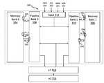
- FIG. 1is a block diagram of exemplary memory device of the present disclosure having dynamic redundancy registers (e1 register 104 and e2 register 106 , in this case).
- FIG. 1shows memory devices 100 described herein that includes memory bank 102 , e1 register 104 , and e2 register 106 .
- memory device 100communicates with data signals, for example, address signal 108 , data word signal 110 , clock signal 112 , write and chip select signals 114 , power down signal 116 , power up signal 118 .
- data signalsfor example, address signal 108 , data word signal 110 , clock signal 112 , write and chip select signals 114 , power down signal 116 , power up signal 118 .
- FIG. 1illustrates certain teachings of the present disclosure. However, it should be understood that the specific signals 108 - 118 illustrated may be modified by those with ordinary skill in the art without departing from the teachings of the present disclosure.
- memory device 100may comprise two or more dynamic redundancy registers and one or more memory banks.
- the two or more dynamic redundancy registerscould be implemented using some combination e1 register 104 and e2 register 106 .
- the two or more dynamic redundancy registersmay also operate hierarchically or in parallel.
- Memory bank 102comprises an array of data storage elements comprising data bits and may be implemented by volatile or non-volatile RAM technologies such as static random-access memory (SRAM), dynamic random-access memory (DRAM), resistive random-access memory (RRAM), phase-change memory (PCM), MRAM, STT-MRAM, or other RAM technologies.
- memory bank 102may include an error correcting code block (not pictured).
- the teachings of the present disclosureare especially beneficial when memory bank 102 comprises STT-MRAM which suffers from an inherently stochastic write mechanism, wherein bits have certain probability of write failure on any given write cycle.
- the teachings of the present disclosureallow memory bank 102 to be operated with high WER. However, many such errors can be corrected using the teachings of the present disclosure. Operating with high WER may allow memory bank 102 to operate under other beneficial conditions. For example, memory bank 102 could operate under high write speed, low write voltage (which may enable higher bitcell endurance), reducing ECC bits, or increased ECC decode speed, among other beneficial conditions.
- memory bank 102may comprise 65,536 ⁇ 50 addressable bits. Further, the 50 bits comprise a 32-bit data word and 18 parity bits for error correction.
- Operationsmay be performed on memory bank 102 including system read, system write, re-write and verify operations, among other data manipulations.
- a particular operationfor example a write operation, may occur at a particular address within memory bank 102 .
- the operationmay have a row address, indicating a word line, and a column address.
- the address for write operationsmay be communicated through a write port of memory bank 102 .
- the address for read or verify operationsmay be communicated through a read port of memory bank 102 .
- memory bank 102comprises a pseudo-dual port memory bank allowing memory device 100 to simultaneously (e.g., substantially within a memory device clock cycle) perform a write operation and a verify operation sharing a common row (word line) address.
- System read operations to memory bank 102generally supersede write and verify operations. Thus, system read operation would be performed before the scheduled write and verify operations. Write and verify operation could then happen on a subsequent clock cycle. If a dual-port memory bank 102 is used, read and write operations may be simultaneously performed.
- the e1 register 104is coupled to memory bank 102 and e2 register 106 .
- the e1 register 104comprises an array of data storage elements comprising data bits and may be implemented by volatile and non-volatile RAM technologies.
- the e1 register 104may also comprise control bits and communicate using control signals that maintain consistency of operations within memory device 100 . Typically, data is more reliably written to e1 register 104 than within memory bank 102 .
- memory bank 102comprises STT-MRAM
- e1 register 104might comprise SRAM.
- e1 registermay comprise non-volatile RAM such as STT-RAM.
- the e1 registermay also comprise a dual-port STT-RAM to allow simultaneous read and write operations. In this case, e1 register 104 can run at the same cycle throughput speed as a memory bank.
- the e1 register 104may also comprise content addressable memory (CAM).
- CAMcontent addressable memory
- e1 register 104stores data words and associated addresses for data in memory bank 102 that has not been verified or has failed verification.
- e1 register 104may store data words that have not been verified.
- e1 register 104receives ROWchg signal that indicates row address change within a pipeline structure of the present disclosure.
- the ROWchg signalindicates that the data word and the associated address from the pipeline structure should be stored within e1 register 104 .
- the ROWchg signalmay also indicate that that another data word and associated address should be transmitted from e1 register 104 to the pipeline structure for verify operation.
- e1 register 104may choose a data word and an associated address such that they share a common row address with a data word in the write register of the pipeline structure. In this way, write operation and verify operation can be simultaneously performed since the data words share a common row address.
- e1 register 104may store data words that have failed verification.
- the pipeline structuremay transmit signal to e1 register 104 indicating that a data word has failed to write (i.e., failed verification) to memory bank 102 .
- the pipeline structuremay also transmit data word and associated address (in the case that e1 register 104 does not already contain the data word and associated address) to e1 register 104 in order to later try to re-write the data word to memory bank 102 .
- read operationmay occur and pipeline structure may determine that read operation did not occur within a predetermined error budget. The pipeline structure may then transmit a signal indicating that the read operation failed and transmit the data word and associated address to e1 register 104 for storage.
- e1 register 104may store data words and associated addresses for future verification. For example, a data word may not have had an opportunity to verify due to row address change. Thus, e1 register 104 may transmit the data word and associated address to the pipeline structure of the present disclosure during some subsequent clock cycle to verify the data word. Typically, a control signal may indicate to e1 register 104 that a row address change will occur or that memory bank 102 will become inactive during subsequent clock cycles. The e1 register 104 may then determine the appropriate data word sharing common row address with data word to be written (in case of row address change) during the subsequent clock cycle. The e1 register 104 then transmits the data word and associated address to verify register of the pipeline structure. In one embodiment, e1 register 104 may also transmit physical address within e1 register 104 if the data word is already stored within e1 register 104 . In this way, control bits associated with the data word may be updated.
- e1 register 104may also store data words for future re-write attempts.
- the e1 register 104may receive data words that have failed verification from the pipeline structure of the present disclosure.
- Memory device 100may have attempted a write operation and the data word failed a verify operation.
- Memory device 100may also have attempted a read operation and the data word may have failed to read within a specified error budget.
- the pipeline structure of the present disclosuremay transmit the data word to e1 register 104 .
- Memory bank 102may become inactive during a subsequent cycle.
- the e1 register 104may then determine an appropriate data word to attempt to re-write to memory bank 102 .
- e1 register 104may transmit a data word and associated address to the pipeline structure.
- the e1 register 104transmits the data word such that a write register could re-write the data word during the clock cycle that memory bank 102 would otherwise be inactive.
- e1 register 102may also relocate data words, associated addresses, and control bits to e2 register 106 . If no more re-write attempts are desired, e1 register 104 may relocate data word and associated address to e2 register 106 . The e1 register may also relocate data to memory bank 102 or e2 register 106 on power down so that data is stored in non-volatile memory in the case that e1 register 104 comprises volatile memory. The e1 register 104 may also relocate data to e2 register 106 in the case that e1 register 104 lacks space for data words.
- the e1 registercomprises control bits and communicates using control signals.
- e1 registercomprises valid bits indicating whether the associated data word is a valid entry within e1 register.
- e1 registercomprises fail count bits indicating the number of re-write attempts associated with a data word. In this way, memory device 100 may try only a specified number of re-write attempts.
- e1 registercomprises bits indicating that the associated data word has not been verified due to row address change and should be verified.
- the e2 register 106is coupled to e1 register 104 and may also be coupled to memory bank 102 .
- the e2 register 106comprises an array of data storage elements comprising data bits and may be implemented by volatile and non-volatile RAM technologies.
- the e2 register 106may also comprise an ECC block and CAM.
- the e2 register 106may comprise data words, associated addresses, and control bits.
- e2 register 106will comprise a non-volatile memory technology, for example STT-MRAM.
- the e2 register 106stores data words and associated addresses relocated from e1 register 104 .
- e2 register 106remaps those data words to addresses within memory bank 102 .
- e2 register 106may store remap addresses in memory bank 102 .
- the e2 register 106then temporarily stores a data word from e1 register and then writes it to an appropriate remap address in memory bank 102 .
- e2 registercontains the appropriate remap address for reading the data word from memory bank 102 .
- Data words and associated addressesmay be relocated to e2 register 106 or remapped based on different conditions.
- e1 register 104relocates data words and associated addresses to e2 register 106 because the data words failed to write to memory bank 102 after the specified number of re-write attempts.
- e1 register 104relocates data words and associated addresses to e2 register 106 because power down signal 116 indicates that data word and associated address should be moved to non-volatile memory, such as e2 register 106 comprising STT-MRAM.
- e1 register 104relocates data words and associated addresses to e2 register 106 because e1 register 104 lacks space.
- control bitsmay also be relocated with associated data word.
- data wordfails to write to a physical address within e2 register 106 after a predetermined number of write attempts a different physical address may be chosen for data word.
- the e2 register 106may also be coupled to an input register of a pipeline structure. In this way, e2 register 106 may receive control signals indicating that a write operation for a data word sharing a common associated address with a data word within e2 register 106 may be occurring. Thus, control bits within e2 register 106 may indicate that a data word within e2 register 106 is invalid because of a system write operation.
- Memory device 100also communicates using exemplary signals 108 - 118 .
- Address signal 108comprises address within memory bank 102 of data to be written to or read from (or otherwise manipulated).
- Data word signal 110comprises a data word to be written to (or otherwise manipulated) memory bank 102 .
- Clock signal 112comprises a memory device 100 clock signal or other clock signal (such as for specific components within memory device 100 ).
- Write and chip select signals 114comprise signals used to determine the operation to be performed within memory bank 102 . For example, if write signal is high and chip select signal is low a read operation might be performed on memory bank 102 .
- Power down signal 116indicates whether power will be removed from memory device 100 or specific components within memory device 100 .
- power down signal 116may be used to determine that contents of e1 register 104 should be written to memory or e2 register 106 .
- Power up signal 118indicates that power is provided to memory device 100 .
- Power up signalmay indicate that e2 non-volatile memory contents should be loaded to e2 volatile memory.
- Power down signal 116may indicate that e2 register 106 volatile memory contents should be moved to e2 register 106 non-volatile memory. For example, e2 register 106 volatile memory contents not already stored in e2 non-volatile memory may be moved to e2 register 106 non-volatile memory. In another embodiment, power down signal 116 may indicate that e2 register 106 contents should be moved to non-volatile memory bank 102 . In another embodiment, power down signal 116 may indicate that certain data words within e1 register 104 should be verified to memory bank 102 . In another embodiment, power down signal 116 indicates that certain data words within e1 register 104 should be re-written to memory bank 102 .
- FIG. 2depicts an exemplary embodiment for a process flow showing a write operation using an exemplary memory device of the present disclosure and illustrates the high-level write operation performed on a memory device.
- a write operation to be performed on primary memorye.g., input register to memory bank 102
- the system write operationmay be performed on primary memory.
- step 206a determination is made whether write operation should be retried in step 206 .
- One retryis illustrated during process flow 200 of FIG. 2 , but as many tries to write data into memory bank may be tried as desired (0 to n retries). If a retry should be tried, the data will be written from e1 register to primary memory when process flow 200 returns to step 202 . From this description a person having ordinary skill in the art will understand the operation of steps 202 - 206 and 210 . However, in some instances, a write operation from e1 register to primary memory may be unsuccessful despite the total desired number of retries.
- step 206if a determination is made at step 206 that no more tries should be made to write data from e1 register to primary memory, process flow 200 will proceed to step 208 .
- step 208data is written to alternate storage (e.g., from e1 register to e2 register).
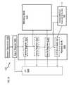
- FIG. 3is a block diagram of exemplary embodiment of a memory device 300 of the present disclosure having dynamic redundancy registers.
- FIG. 3is a block diagram of memory device 300 described herein that include memory banks 304 and 306 , pipeline banks 308 and 310 , input register 312 , e1 register 314 , and e2 register 316 .
- Memory device 300communicates using signals 318 - 324 .
- Memory device 300includes ports 326 - 336 for performing read, write, and verify (or other data manipulation) operations on memory banks 304 and 306 .
- Memory device 300is described herein to describe aspects of the present disclosure. One of ordinary skill would understand how to modify memory device 300 without departing from the teachings of the present disclosure.
- memory device 300may comprise two or more dynamic redundancy registers and one or more memory banks.
- Memory banks 304 and 306have previously been described with respect to FIG. 1 .
- Memory banks 304 and 306also include two ports ( 326 and 328 ; 332 and 334 , respectively) for performing read, write, and verify (or other data manipulation) operations.
- Memory bank 304could, for example, comprise data words having even addresses while memory bank 306 comprises data words having odd addresses.
- Two ports 326 and 328 of memory bank 304are coupled to bit lines of memory bank 304 .
- two ports 332 and 334 of memory bank 306are coupled to bit lines of memory bank 306 .
- memory device 300may comprise any desired number of read and write ports. In one embodiment, a dual port memory bank is used.
- each port 326 - 336could perform simultaneous read and write operations.
- each port 326 - 336could perform simultaneous read and write operations.
- pseudo-dual port memory banks 304 - 306in mind to highlight specific teachings of the present disclosure.
- the Y-mux structure of the present disclosureallows pseudo-dual port memory banks 304 - 308 to perform simultaneous write and verify operations sharing common row address and different column address.
- write port 326allows transmission of signals comprising write address and write data to memory bank 304 from pipeline bank 308 .
- Port 328allows transmission of data signals comprising read address or verify address to memory bank 304 from pipeline bank 308 .
- Port 330allows transmission of data signals comprising read data word from memory bank 304 to pipeline bank 308 .
- Pipeline banks 308 and 310comprise data registers for implementing the write, read, and verify (and other data manipulation) operations of the present disclosure.
- Pipeline banks 308 and 310are coupled to memory banks 304 and 306 , respectively, using pseudo-dual port structures, as explained above, for providing simultaneous write and verify operations.
- pipeline banks 308 and 310are coupled to input register 312 .
- pipeline banks 308 and 310implement a pipeline structure that allows verify and write operations to be simultaneously performed on memory banks 304 and 306 .
- pipeline bankscommunicate with e1 register 314 to implement a pipeline structure of the present disclosure.
- Input register 312comprises data storage elements comprising data bits. Input register comprises a data word, an associated addresses within memory banks, and control bits indicating a system operation such as system read or system write. For example, input register 312 may comprise a data word to be written to memory banks (received from data signal 322 ), the address of the data (received from address signal 324 ), and control bits. Input register 312 may be coupled to pipeline bank 308 and pipeline bank 310 to communicate a data word, its associated address, and control bits.
- input register 312may be coupled to e1 register 314 for transferring the associated address of data word to e1 register 312 and control signals.
- the e1 register 314has been described in connection with FIG. 1 , and will also be further described in connection with FIG. 7 .
- the e1 register 314is coupled to pipeline banks 308 and 310 and e2 register 316 .
- the e1 register 314comprises data storage elements comprising data bits.
- e1 register 314may comprise data word and associated addresses for data words that have failed to verify correctly within memory banks 304 and 306 .
- the e1 register 314may comprise data words and associated addresses for data words that have not yet been verified within memory banks 304 and 306 .
- the e1 register 314may also comprise data words and associated addresses for data words that have failed to read from memory banks 304 and 306 within an associated error budget.
- the e2 register 316has been described in connection with FIG. 1 , and will also further be described in connection with FIG. 8 .
- the e2 register 316may be coupled to e1 register 314 .
- the e2 register 316comprises data storage elements comprising data bits.
- the e2 register 316comprises data words, associated addresses, and control bits. These data words have typically failed to write to memory banks 304 and 306 . These words may have also been written from e1 register 314 to e2 register 316 because of power down of memory device 300 or lack of space within e1 register.
- e2 register 316may optionally be coupled to pipeline banks 308 and 310 or memory banks 304 and 306 in order to write data words (or other signals).
- e2 registermay store remap addresses within memory banks 304 and 306 for writing directly to memory banks through a remap process.
- e2 register 316writes data to memory banks 304 and 306 during power down.
- FIG. 4is a block diagram of exemplary embodiment of a memory device of the present disclosure showing a Y-mux structure.
- FIG. 4shows portion of memory device 400 comprising memory bank 402 , row decoder 404 , write column decoder and y-mux 406 , read column decoder and y-mux 408 , and muxes 410 - 412 .
- FIG. 4shows a Y-mux structure for decoders 406 - 408 .
- the Y-mux structureallows simultaneous verify and write operations for data words sharing a common row address (word line) in the memory bank but different column address.
- Memory bank 402is coupled to decoders 404 - 408 .
- Row decoder 404takes as an input the row of address for data word that is to be written to or read or verified from memory bank 402 . Row decoder then determines appropriate row for the data word.
- a data wordis a pre-defined number of bits for a piece of information handled by a memory device. For example, a data word may comprise 8, 16, 24, etc. bits. The size of a data word is dependent on the memory device and may be varied as necessary.
- Mux 410is coupled to row decoder 404 .
- Mux 410takes as inputs the pipeline row address (Pipeline_A_Row) and read row address (Read_A_Row).
- Pipeline row addressindicates the row address for data words received from the pipeline for either a write or verify operation.
- the pipeline row addressindicates a shared row address between a data word to be written to memory bank 402 and another data word to be simultaneously verified in memory bank 402 .
- Read row addressindicates a row address for a data word to be read from memory bank 402 .
- Read row addressgenerally takes precedence over pipeline row address when pseudo-dual port memory bank 402 is used.
- Mux 410then outputs appropriate row address to row decoder 404 .
- Row address decoder 404then activates the appropriate row in memory bank 402 . Appropriate activation schemes will be known to those with ordinary skill in the art.
- Write column decoder and y-mux 406is coupled to memory bank 402 .
- Write column decoder and y-mux 406takes as inputs write address column WR_A_Col and write data WR_D, such as data word.
- Write address columnindicates a column address for a system write or re-write operation received from the pipeline structure of the present disclosure.
- Write column decoder and y-mux 406determines appropriate column address for write operation.
- Write column decoder and y-mux 406then activates the appropriate column in memory bank 402 . Appropriate activation schemes will be known to those with ordinary skill in the art.
- Read column decoder and y-mux 408is coupled to memory bank 402 .
- Read column decoder and y-mux 408takes as its input the column address output from mux 412 .
- Read column decoder and y-mux 408determines the appropriate column for read operation.
- Read column decoder and y-mux 408then activates the appropriate column in memory bank 402 . Appropriate activation schemes will be known to those with ordinary skill in the art.
- Mux 412is coupled to read column decoder and y-mux 408 .
- Mux 412takes as inputs pipeline column address (Pipeline_A_Col) and read column address (Read_A_Col).
- Pipeline column addressindicates column address of data word that should be verified in memory bank 402 .
- Pipeline column addressis received from the pipeline structure.
- Read column addressindicates a column address for a data word that should be read from memory bank 402 .
- read column addresstakes precedence when a pseudo-dual port memory bank 402 is used.
- Mux 402outputs signal comprising column address for read operation or verify operation to read column decoder and y-mux 408 .
- row and column decoders 404 - 408perform operation on specific addresses within memory bank 402 (for example, read, write, or verify).
- Y-mux structure of column decoders and y-mux 406 - 408allows memory bank 402 to be operated as a pseudo-dual port memory bank.
- a single port memory cellmay thus be used, but memory bank 402 may simultaneously perform verify and write operations when those operations share a common row address but different column addresses. If a dual port memory bank 402 was used, read and write or verify and write operations could be performed simultaneously.
- FIG. 5is a block diagram of exemplary embodiment of a memory device of the present disclosure showing pipeline structure that allows verification and re-write operations.
- FIG. 5shows exemplary pipeline 500 for implementing the pipeline flow for system write, re-write, and verify operations, among other data manipulation operations.
- Pipeline 500is implemented using system operations 502 , input register 504 , pipeline bank 506 , e1 register 508 , and memory bank 510 .
- Pipeline bank 506comprises write register 512 , delay register 514 , verify register 516 , and verify results register 518 .
- pipeline 500comprises compare memory logic 520 .
- System operation 502comprises signals for performing a desired operation such as system write and system read, among other data manipulation operations.
- system operation 502typically includes signals indicating a data word, the associated data address within memory bank 510 , and control signals indicating the operation to be performed on memory bank 510 (such as write or chip select signal), among other signals for performing data manipulation operations and maintaining appropriate states.
- the signals from system operation 502are stored in input register 504 .
- Other configurations for signals from system operation 502may be used without departing from the scope of the present disclosure.
- other embodiments of pipeline 500are possible without departing from the teachings of this disclosure.
- delay register 514allows delay between write and verify operation on a data word.
- STT-MRAMmay require a delay between write operations at a particular address and verify operation at the common address.
- the delay cycleallows data storage elements within memory bank 510 to return to a stable state before performing verify operation.
- Other RAM technologies, and in some instances STT-MRAM itself,may not require such delay and delay register 514 is not necessary.
- Input register 504is coupled to write register 512 .
- Input register 504comprises data storage elements comprising data bits.
- input register 504can include data bits for a data word, associated address, a valid bit, and other desired control bits.
- the valid bitindicates whether data manipulation operations such as system write operation should be performed or the register should not be used to perform such operations.
- valid bits based on a write signal and chip select signal provided by system operation 502may indicate whether data word in input register is used for write.
- Input register 504may also be coupled to e1 register 508 , for example, to transmit associated address and control bits to e1 register 508 . This associated address and control bits may be used in case of row address change in the pipeline or to invalidate an e1 register 500 entry with the same associated address, for example.
- An active memory bank of an embodiment of the present disclosuredenotes a memory bank in which a system write or system read is taking place.
- an active bank signal(or an active bank bit) prevents re-writes during that clock cycle, and instead indicates that a system write or read will occur during that clock cycle.
- an active bank signalindicates that write register 512 will write a data word previously received from input register 504 to memory bank 510 during that clock cycle.
- e1 registerknows that data word for re-write operation should not be transmitted to write register 512 during that clock cycle.
- Input register 504transmits data word, associated address, and desired control bits to write register 512 .
- the e1 register 508has previously been described with respect to FIG. 1 and will be described in conjunction with FIG. 7 .
- the e1 register 508is coupled to input register 504 , write register 512 , delay register 514 , verify register 516 , and verify results register 520 .
- the e1 register 508may supply data word, associated address of a data word within memory bank 510 , and control signals to write register 512 , and verify register 516 .
- the e1 register 508may receive a data word, its associated address, and control signals from delay register 514 and verify results register 518 .
- the e1 register 508may also transmit a physical address within e1 register 508 in case the data word is already stored within e1 register 508 .
- e1 register 508may receive data word, associated address, and control signals from write register 512 . Moreover, e1 register 508 may communicate with input register to receive signals such as data word signal and control signal such as inactive bank signal.
- Write register 512is coupled to delay register 514 and memory bank 510 . In other embodiments, write register 512 may be coupled to verify register 516 .
- Write register 512comprises data storage elements comprising data bits. Typically, write register 512 comprises data bits for a data word, its associated address, valid bit, and other desired control bits. The valid bit is a valid register bit and may be set to one when write register 512 contents are valid such that write operation may occur.
- Write register 504receives data word, associated address, and desired control bits from input register 504 for system write operations. For memory bank clock cycles that write register 504 would not otherwise be writing system data words to that memory bank, e1 register 508 transmits data words, associated address, and desired control bits to write register 512 .
- write register 512This allows write register 512 to attempt re-write operations when write register 512 would not otherwise be writing system data words to memory bank 510 .
- read operationsgenerally take precedence over write operations from write register 512 .
- write register 512may perform write operation simultaneously with verify operation performed by verify register 516 if the operations share a common row address.
- Write register 512also transmits data word, associated address, and desired control bits to delay register 514 (or verify register 516 if no delay register is used).
- Delay register 514is coupled to verify register 516 and e1 register 508 .
- Delay register 514comprises data storage elements comprising data bits.
- delay register 514comprises a data word, associated address bits, a valid bit, and other desired control bits. Valid bit indicates if delay register 514 contents are valid.
- the delay register or multiple delay registercould provide more clock cycle delay between write and verify.
- the delay register 514is optional for RAM technologies that require delay between write and verify operations for a particular address within memory bank 510 . If row address change occurs within pipeline bank 504 , delay register 514 transmits data word, associated address, and desired control bits to e1 register 508 .
- data wordmay be verified on a later clock cycle when write register will write a data word sharing a common row address.
- data wordmay be verified on a later clock cycle when no verify operation will otherwise occur to the memory bank. If no row address change occurs within pipeline bank 504 , after desired delay clock cycles, delay register 514 transmits the data word, associated address, and desired control bits to verify register 516 .
- Verify register 516is coupled to memory bank 510 and verify results register 520 .
- Verify register 516comprises data storage elements comprising data bits. Typically, verify register 516 comprises a data word, its associated address, valid bit, and other desired control bits. Verify register 156 may comprise internal e1 address if data word was received as a result of re-write operation or verify operation from e1 register. Valid bit indicates whether verify register 516 contents are valid for verify operation. Verify register 516 contents, such as data word, can be sourced from either delay register 514 (or write register 512 in case delay register 512 is not used) or e1 register 508 . Verify register 516 would receive contents from delay register 514 if no row address change has occurred.
- Verify register 516would receive contents from e1 register 508 if row address change occurred.
- verify register 516receives the data word, its associated address, address within e1 register, fail count bits, and other desired control bits from e1 register 508 .
- Verify register 516transmits the associated address to memory bank 510 for the data word to be verified.
- Verify register 516transmits the data word, fail count bits, and other desired status bits to compare data logic 520 .
- Verify register 516transmits the data word and its associated address to verify results register 518 in case of a system write.
- Verify register 516transmits internal e1 address in case of re-write operation or verify from e1 register 508 . Thus, if the data word and the associated address already exist e1 register 508 , verify register 516 need not transmit the data word and the associated address to verify results register 518 .
- Compare memory logic 520is coupled to verify register 516 .
- Compare memory logic 520comprises data storage elements comprising data bits.
- Compare memory logic 520may comprise read or sense amplifiers to read a data word from memory bank 510 .
- Hardware logic for implementing compare memory logic 520can be used by those with ordinary skill in the art.
- compare memory logic 520receives input from verify register 516 and memory bank 510 .
- Memory bank 510outputs a data word to compare memory logic 520 based on the associated address transmitted from verify register 516 .
- Compare memory logic 520also receives the data word from verify register 516 .
- compare memory logic 520determines whether the write operation passed or failed.
- Compare memory logic 520makes the pass/fail determination based on methods desired by those with ordinary skill in the art. In one embodiment, compare memory logic 520 determines whether the data word from verify register 516 matches the data word from memory bank 510 . In other embodiments, compare memory logic 520 deems that the operation passed if a predetermined number of bits match.
- compare memory logic 520passes appropriate control bits to verify results register 518 , for example fail count bits may be set to 0. Verify results register 518 may then invalidate the entry within e1 register if needed. If verify operation failed, verify results register 518 updates fail count bits within e1 register (in case of re-write or verify from e1) or transmits the data word, the associated address, and control bits to e1 register (in case of system write).
- memory bank 510outputs a data word, the associated address, and desired control bits to compare memory logic 520 .
- Compare memory logic 520determines whether the read operation passed or whether re-write operation should be performed on memory bank 510 because too many errors occurred while reading the data word.
- compare memory logic 520corrects data words using ECC and parity bits associated with data words. If ECC determines that too many errors occurred (e.g., errors above a predetermined threshold), compare memory logic 520 also transmits the data word and control bits to verify results register 518 .
- Verify results register 518is coupled to compare memory logic 520 and e1 register 508 .
- Verify results register 518comprises data storage elements comprising data bits. Typically, verify results register 518 comprises data bits for a data word, associated address, valid bit, and desired control bits. Valid bit indicates that contents of verify results stage register 518 are valid to be written to e1 register 508 .
- Verify results register 518may also comprise internal e1 address. Verify results register 518 transmits data to e1 register as previously explained.
- pipeline structure 500is exemplary and may include more write, delay, verify, verify results registers, and compare logic blocks to allow more re-write attempts before writing failed data words to e1 register. Moreover, more registers and memory banks may be added without departing from the scope of the present disclosure.
- FIG. 6is an exemplary process flow showing an embodiment of a system read operation using an embodiment of memory device of the present disclosure.
- FIG. 6shows process flow 600 for system read operation of the present disclosure.
- Process flow 600illustrates the high-level read operation performed on a memory device.
- a system read operation to be performed on memory bankexists within a memory device.
- the valid address stored in both pipeline banksare checked to determine whether the data word associated with system read operation exists there. If no, e1 register checks address to determine whether the data word associated with system read operation exists there in step 606 . If no, e2 register checks the address to determine whether the data word associated with system read operation exists there in step 608 .
- step 608If no, the data word is read from memory bank at the associated address of system read operation in step 610 . If the result of step 608 is yes, the data word is read from e2 register in step 618 . If the answer to step 604 returned yes, then data word is read from pipeline 614 . If the answer to step 606 is yes, then the data word is read from e1 register in step 616 .
- One of ordinary skill in the artmay recognize other process flows for system read operations without departing from the teachings of the present disclosure.
- System read process flow 600may include additional steps. After step 610 , compare logic may determine whether system data word from memory bank was read within a predetermined error budget in step 612 . If the data word output from memory bank contains errors, such errors may be corrected though ECC. If the data word output from memory bank contained more errors than allowed by a predetermined error budget, the data word may also be corrected and stored in e1 register in step 619 . In this way, e1 register may attempt to re-write data word back to memory bank so that the data word may be read within a predetermined error budget on future read operations. The corrected data word and associated address would be stored within e1 register.
- FIG. 7is a block diagram of an embodiment of a memory device showing a first level dynamic redundancy register.
- FIG. 7shows exemplary e1 register 700 described herein that comprises physical address decoder 702 , CAM 704 , mux 706 , RAM 708 , status logic 710 , and control logic 712 .
- e1 register 700is exemplary, and includes features such as CAM 704 which are not required for achieving the teachings of the present disclosure.
- e1 register 700communicates control signals for maintaining consistency of operations both internally and to communicate with components of memory device such as pipeline banks and e2 register. Such control signals may be modified without departing from the teachings of the present disclosure.
- Physical address decoder 702is coupled to CAM 704 , mux 706 , and control logic 712 . Physical address decoder 702 receives an address input from control logic 712 . Physical address decoder 702 uses the address input to determine the appropriate physical addresses within CAM 704 and RAM 708 for performing data manipulation operation, such as read and write. Physical address decoder 702 selects an entry within CAM 704 using decode signal. Physical address decoder 702 may also select an entry within RAM 708 using decode signal to mux 706 .
- physical address decoder 702may take pointers as input from control logic 712 .
- Different pointers from control logic 712indicate available addresses for writing data to CAM 704 and RAM 708 or reading data from CAM 704 and RAM 708 , or other pointers may be used.
- pointers from control logic 712may keep track of lowest open addresses within CAM 704 and RAM 704 .
- e1 register 700keeps track of addresses for storing new data.
- Pointers from control logic 712may also keep track of oldest stored data within CAM 704 and RAM 708 .
- re-write operationsmay be tried on a First-In-First-Out (FIFO) basis.
- FIFOFirst-In-First-Out
- CAM 704is coupled to mux 706 .
- CAM 704takes as input decode signal from physical address decoder 702 .
- CAM 704also takes as input an associated address which may be received from input register, delay register, or verify results register of a pipeline structure.
- CAM 704also takes as input control bits such as read, write, or search signal received from control logic 712 .
- CAM 704also takes as input other control bits from status logic 710 .
- the associated address signalsindicate addresses within a memory bank.
- Associated address signalis typically received from input register, delay register, or verify results register.
- e1 register 700receives an address within a memory bank where data word should be verified or written.
- the e1 register 700may also receive associated address from input register to be searched for words with matching row addresses which may be verified.
- CAM 704will typically write associated address from delay register or verify results registers to itself, so that associated address may be used later for re-write or verify operation.
- Status signalsuch as valid bit, indicates whether physical address within CAM 704 contains valid data for data manipulation operation.
- CAM 704may receive status signal from status logic 710 .
- Read signalindicates that CAM 704 should output an associated address, and RAM 708 should output the corresponding data word.
- CAM 704may use decode and read signal to output an associated address of the data word stored in RAM 708 .
- CAM 704may output an associated address of the data word to write register. In this way, write register may write data from e1 register in a clock cycle during which it would otherwise be inactive.
- Write signalindicates that the associated address should be stored within CAM 704 and the corresponding data word should be stored within RAM 708 .
- CAM 704may use the associated address signal, decode signal, and write signal to write the associated address to a physical address within CAM 704 . In one embodiment, this may occur because row address change occurred within pipeline structure and delay register sent a data word, an associated address, and control bits to e1 register 700 for storage. In another embodiment, verify results register may send a data word, an associated address, and control bits to e1 register 700 for storage because verify operation failed or data was not read within a predetermined error budget.
- Search signalindicates that CAM 704 should search itself for an appropriate address.
- CAM 704uses search signal received from control logic 712 to search itself for an associated address to output to verify register.
- search signalreceived from control logic 712 to search itself for an associated address to output to verify register.
- CAM 704may output the associated address of a data word sharing a common row address with the data word to be written from the pipeline.
- e1 RAM 708outputs a data word matching the associated address within CAM 704 to the pipeline.
- CAM 704outputs associated addresses to the pipeline structure, such as to write register and verify register. CAM 704 also outputs associated addresses to e2 register. CAM 704 may only output a portion of associated address. For example, if row address change occurred and CAM 704 searched itself for an appropriate address for verify operation, CAM 704 may output only the column address since the row address may be known. CAM 704 also outputs match signal to mux 706 . Match signal indicates the physical address within RAM 708 of a data word that corresponds to the associated address within CAM 704 . Match signal may be used when reading a data word from RAM 708 .
- Mux 706takes as input read, write, search signal from control logic 712 .
- Mux 706also takes as input decode signal received from physical address decoder.
- Mux 706also takes as input match signal from CAM 704 . Mux then transmits select signal to RAM 708 for data manipulation operation. If mux 706 receives read signal, mux 706 typically transmits decode signal to RAM 708 because decode signal indicates the physical address within RAM 708 for read operation. If mux 706 receives write signal, mux 706 typically transmits decode signal to RAM 708 because decode signal indicates the physical address within RAM 708 for write operation. If mux 706 receives search signal, mux 706 typically transmits match signal to RAM 708 because match signal indicates the physical address within RAM 708 for outputting data word.
- RAM 708takes as input select signal from mux 706 .
- RAM 708also takes as input a data word received from pipeline structure, such as from delay register or verify results register.
- RAM 708also takes as input read and write signals received from control logic 712 .
- Select signal from mux 706indicates the physical address within RAM 708 for performing data manipulation operation such as read or write operation.
- Data word signalindicates the data word for storage within RAM 708 .
- Read signalindicates whether the physical address signal should be used for read operation such that data should be read from RAM 708 and output to pipeline structure or e2 register.
- Write signalindicates whether select signal should be used for write operation such that data word signal should be written to RAM 708 .
- RAM 708typically comprises volatile memory such as SRAM, but may comprise non-volatile memory such as STT-MRAM.
- Status logic 710comprises hardware logic that drives the selection of addresses within control logic 710 .
- Status logic 710takes as input control signals from pipeline structure and e2 register. Control signals may include ROWchg flag previously discussed. Pipeline structure may also transmit fail count bits to status logic 710 .
- status logic 710updates a valid bit associated with a data word to invalid in the case that status logic 710 receives fail count bits set to 0. That is, because control signals received from verify results register indicated that verify operation passed, e1 register 700 invalidates the entry associated with data word (associated addresses, data word, any associated control bits).
- Status logicmay also take as input inactive signal indicating that memory bank may become inactive during a subsequent clock cycle.
- e1 registershould output a data word to write register for a re-write operation.
- Status logic 710may also receive control signals from e2 register. For example, status logic 710 may receive signal indicating that e2 register is ready for a new data word. Status logic 710 may also receive decode signal from physical decoder 702 . Decode signal will indicate the entry or entries within e1 register 700 which are being updated.
- Status logic 710transmits status signals. Status logic 710 transmits status signals both internally and externally. Status logic 710 transmits status signals to control logic 710 . Status logic 710 may also transmit status signals, such as fail count bit, to pipeline structure and e2 register. Thus, control signals from status logic 710 may be used to maintain consistency of operations both within e1 register 700 and within pipeline structure.
- Control logic 712comprises hardware logic for determining operations to be performed on CAM 704 and RAM 708 .
- Control logic 712also comprises hardware logic for outputting address signal to physical address decoder 702 .
- Control logic 712takes as input status signals from status logic 710 . Status signals drive the selection of addresses by control logic 712 . For example, status signals may indicate that write operation should be performed on CAM 704 and RAM 708 .
- Control logicmay then increment a pointer to next address, indicating empty addresses within CAM 704 and RAM 708 for writing associated addresses and data words.
- the address signal output from control logic 712may comprise pointers that are decoded by physical address decoder 702 to select appropriate physical addresses within CAM 704 or RAM 708 for performing data manipulation operation.
- the address signal output from control logic 712may also be output to the pipeline to indicate physical addresses within e1 register 700 .
- e1 register 700may transmit a data word, its associated address, and its physical address within e1 register 700 to pipeline structure.
- the physical address within e1 register 700may be used to update e1 register 700 control bits after verify or re-write operation occurs. If the re-write operation failed, for example, fail count bits within e1 register 700 may be updated using the physical address within e1 register 700 .
- FIG. 7illustrates one of many possible implementations of e1 register 700 .
- Other implementations of e1 register 700may be used in conjunction with the teachings of the present disclosure.
- FIG. 8is a block diagram of an embodiment of a memory device of the present disclosure showing a last level dynamic redundancy register.
- FIG. 8shows exemplary e2 register 800 described herein that comprises CAM/RAM/Enbl/Pointers block 802 , mux 816 , e2 RAM 818 , and physical y-mux 832 , sense amplifier 834 , error correction code bits 836 , write register 838 , and control logic 840 .
- e2 register 800is exemplary, and includes features such as RAM Memory bank FC 814 which are not necessary for achieving the teachings of the present disclosure.
- e2 register 800communicates control signals for maintaining consistency of operations both internally and to communicate with components of memory device such as pipeline banks, memory banks, and e1 register. Such control signals may be modified without departing from the teachings of the present disclosure.
- CAM/RAM/Enbl/Pointers block 802comprises physical address decoder 804 , address CAM 806 , RAM update flag 807 , RAM enable 808 , RAM e2 fail count 810 , RAM used count 812 , and RAM memory bank FC 814 .
- block 802comprises data storage elements comprising data bits. Block 802 is used for storing control bits and associated addresses of data words.
- Physical address decoder 804receives an address inputs from control logic 840 . As explained in relation to e1 register and FIG. 7 , physical address decoder 804 uses address inputs to determine physical addresses for writing associated addresses and data words to CAM 806 and RAM 818 , respectively. Physical address decoder 804 outputs decode signal to CAM 806 and mux 816 . Moreover, physical address decoder 804 may output decode signal to physical y-mux 832 .
- CAM 806stores associated addresses for data words. As explained in relation to e1 register and FIG. 7 , CAM 806 may take as inputs various control signals and associated addresses. CAM 806 can then write associated addresses to itself or determine appropriate physical address within RAM 818 for matching data word. Typically, such data word would be output, for example, to pipeline banks or memory banks.
- RAM update flag 807comprises control bits for determining whether associated data should be updated within RAM 818 . For example, control signals received from control logic 840 may indicate that RAM 818 entry should be updated based on a new data word. RAM update flag 807 thus provides a mechanism to track data words that should be updated in case it is not possible to update the data word immediately.
- RAM enable 808comprises control bits indicating whether e2 RAM 818 contains a valid data word. RAM enable 808 may thus require that all bits be set to one, for example, to provide a stringent mechanism to ensure that RAM 818 includes valid data. RAM enable 808 may be output to control logic 840 so that control logic may keep track of valid data within block 802 and RAM 818 .
- One of ordinary skill in the artwill recognize that other schemes may be used to ensure reliability of data words. For example, multiple copies of data word may be maintained in RAM 818 and selected based on a voting scheme. In another scheme, a more stringent error correction code (ECC) scheme may be performed within e2 register 800 than in memory bank. In another scheme, RAM 818 points to particular addresses within main memory for storing data words rather than storing the data words within e2 register 800 itself.
- ECCerror correction code
- RAM e2 fail count 810indicates the number of times a data word has failed to write to e2 RAM 818 .
- RAM 818may comprise non-volatile STT-MRAM in an embodiment.
- e2 register 800may write to RAM 818 until write operation is successful in order to maintain reliability within e2 register 800 .
- e2 fail countindicates the number of times a data word has failed to write to RAM 818 .
- RAM e2 fail count 810may be output to control logic 840 , so that control logic 840 may output appropriate addresses for writing to RAM 818 .
- RAM used count 812indicates the number of times that a physical address within e2 RAM 818 has been used.
- the e2 register 800may desire to keep track of the number of times that a particular physical address within RAM 818 has been used. For example, the number of times that a read operation has occurred, write operation has occurred, or both to a specific physical address within RAM 818 .
- RAM memory bank FC 814indicates the number of times that a data word has failed to write to a memory bank.
- e2 register 800may desire to keep track of the number of times that a write operation from e2 register 800 has failed to the memory bank. This may be useful so that only a desired number of re-write operations are tried.
- the specific components of block 802are exemplary and may be modified without departing from the teachings of the present disclosure.
- RAM memory bank FC 814is optional and provides a mechanism for controlling the number of re-write attempts to memory bank.
- Mux 816is coupled to CAM/RAM/Enbl/Pointers block 802 and e2 RAM 818 .
- Mux 816takes as input decode signal from physical address decoder 804 indicating physical address within e2 RAM 818 and match signal from CAM 806 indicating that match exists within e2 RAM 818 .
- e2 RAM 818can perform read or write operation. If e2 RAM 818 comprises MRAM, write operations may be tried a number of times based on RAM e2 fail count 810 . In another embodiment, after a predetermined number of write attempts to physical address within e2 RAM 818 , RAM used count 812 may operate to indicate that another location within e2 RAM 818 should be chosen for write operation.
- the e2 RAM 818comprises RAM data 820 , RAM address 822 , RAM enable 824 , RAM used count 826 , and Memory Bank FC 830 .
- the e2 RAM 818may comprise volatile or non-volatile memory.
- the e2 RAM 818comprises non-volatile memory such as MRAM so that contents may be saved on during power down.
- RAM data 820comprises data storage elements comprising data bits storing a data word received from e1 register.
- RAM address 822stores an associated address within a memory bank for the data word stored within RAM data 820 .
- CAM 806may store an associated address to RAM address 822 .
- RAM enable 824stores the same enable bits as RAM enable 808 .
- RAM used count 826stores the same used count as in RAM used count 812 .
- Memory Bank FC 830stores the same fail count as RAM Memory Bank FC 814 .
- block 802 comprising volatile storagee.g., SRAM
- non-volatile storagee.g., MRAM
- y-mux 832allows read and write operations to be performed on RAM 818 .
- Sense amplifiers 824are used to read RAM 818 .
- ECC block 836allows error correcting on RAM 818 .
- Write Register 938may comprise CAM for searching write register contents. Write register 838 receives data word and address from e1 register. Write register 838 also communicates with e2 control logic 840 to, for example, send ready e2 ready signal when write register 838 is ready for new data word from e1 register.
- Control logic 840comprises hardware logic. Control logic 840 determines appropriate operations (such as read, write, and search) to be performed on e2 register 800 . Control logic 840 also determines addresses. As previously explained in connection with FIG. 7 , control logic 840 may use many different addressing schemes. In one embodiment, control logic 840 uses pointers to determine physical addresses within block 802 and RAM 818 for writing data words. Control logic 840 may also communicate with other components of memory device including pipeline banks, memory banks, and e1 register. For example control logic 840 transmits e2 flag to e1 register to indicate that e2 register 800 may receive a new data word to write register 838 .
Landscapes
- Engineering & Computer Science (AREA)
- Computer Hardware Design (AREA)
- Theoretical Computer Science (AREA)
- Physics & Mathematics (AREA)
- General Engineering & Computer Science (AREA)
- General Physics & Mathematics (AREA)
- For Increasing The Reliability Of Semiconductor Memories (AREA)
- Techniques For Improving Reliability Of Storages (AREA)
Abstract
Description
- The present application is a Divisional of, claims the benefit of and priority to U.S. application Ser. No. 15/277,799 Attorney Docket SPIN-0002-01.01, filed Sep. 27, 2016, entitled “DEVICE WITH DYNAMIC REDUNDANCY REGISTERS” and hereby incorporated by reference in its entirety.
- The present patent document relates to registers that are added to devices, and more particularly registers added to random access memory (RAM). The methods and devices described herein are particularly useful in spin-transfer torque magnetic memory (STT-MRAM) devices.
- Magnetoresistive random-access memory (“MRAM”) is a non-volatile memory technology that stores data through magnetic storage elements. These magnetic storage elements are two ferromagnetic plates or electrodes that can hold a magnetic field and are separated by a non-magnetic material, such as a non-magnetic metal or insulator. In general, one of the plates has its magnetization pinned (i.e., a “reference layer”), meaning that this layer has a higher coercivity than the other layer and requires a larger magnetic field or spin-polarized current to change the orientation of its magnetization. The second plate is typically referred to as the free layer and its magnetization direction can be changed by a smaller magnetic field or spin-polarized current relative to the reference layer.
- MRAM devices store information by changing the orientation of the magnetization of the free layer. In particular, based on whether the free layer is in a parallel or anti-parallel alignment relative to the reference layer, either a “1” or a “0” can be stored in each MRAM cell. Due to the spin-polarized electron tunneling effect, the electrical resistance of the cell changes due to the orientation of the magnetization of the two layers. The cell's resistance will be different for the parallel and anti-parallel states and thus the cell's resistance can be used to distinguish between a “1” and a “0.” MRAM devices are generally considered as non-volatile memory devices since they maintain the information even when the power is off. The two plates can be sub-micron in lateral size and the magnetization direction can still be stable with respect to thermal fluctuations.
- MRAM devices are considered as the next generation structures for a wide range of memory applications. MRAM products based on spin torque transfer switching are already making its way into large data storage devices. Spin transfer torque magnetic random access memory (“STT-MRAM”) has an inherently stochastic write mechanism, wherein bits have certain probability of write failure on any given write cycle. The write failures are most generally random, and have a characteristic failure rate. A high write error rate (WER) may make the memory unreliable.
- In memory devices, and especially STT-MRAM, methods and systems for verifying and re-writing data words are beneficial.
- In an embodiment, a device with dynamic redundancy registers is disclosed. In one aspect, a memory device comprising random access memory (RAM) device, and specifically an STT-MRAM device, is provided. The present disclosure provides backup dynamic redundancy registers that allow the device to operate with high write error rate (WER). The dynamic redundancy registers allow verifies, re-writes, and relocation of data words that fail to write correctly to a memory bank, generally, without loss of throughput, speed, or restriction on random access addressing.
- In one aspect, the present disclosure teaches a memory bank that is coupled to an e1 register. The e1 register is coupled to the e2 register. The e1 register stores data words that are to be verified or re-written to the memory bank. The e1 register also stores an associated address for data words within the memory bank. Data words in the e1 register may be verified against data words in the memory bank at the associated address within the memory bank. If a system write operation fails on the memory bank, a re-write operation may be tried by writing a data word from the e1 register to the memory bank. The fact that the system write operation failed may be determined through a verify operation. Re-write operation from e1 register to memory bank may be tried as many times as necessary to successfully complete write operation or may not be tried at all. In one example, the number of re-write operations may be configurable based on control bit(s) associated with re-write attempts. In one aspect, the number of re-write operations may be configurable on a per-bank basis or per-segment of bank basis. These control bits may be stored in the e1 register and associated with a particular data word and communicated and updated as appropriate.
- In one aspect, the re-write operation may be tried only when memory bank is idle (that is there are no write or read operations for that memory bank). In this way, re-write operations may be transparent to and with no delay of incoming system read and system write operations. After the desired number of re-write attempts (0 to n) from the e1 register, the memory device moves (relocates) data word from the e1 register to the e2 register. The memory device may also move associated address within memory bank for data word from the e1 register to the e2 register. In one embodiment, a re-write operation may occur only once from the e1 register to the memory bank. The memory device then relocates the data word and associated address from the e1 register to the e2 register if the re-write operation failed. Although explained with reference to one memory bank and two dynamic redundancy registers, one or more memory banks and two or more dynamic redundancy registers may also be used.
- Typically, the first level dynamic redundancy register (e1 register) may operate at clock cycle speed of memory bank (some operations may operate at clock cycle speed of memory bank while other operations may occur independent or multiples of memory bank clock cycle speed). The e1 register may be either non-volatile or volatile, and may typically comprise SRAM. The e1 register may also comprise a content addressable memory (CAM) array which allows reduced size of e1 register. In one embodiment, e1 register may be high-speed, smaller register than a last level register.
- Typically, the last level dynamic redundancy register (e2 register) may operate at clock cycle speed of main memory bank (some operations may operate at clock cycle speed of memory bank while other operations may occur independent or multiples of memory bank clock cycle speed). The last level may be either non-volatile or volatile, and may typically comprise MRAM. The e2 register may also comprise a CAM. The last level dynamic register may beneficially comprise non-volatile memory which allows data to be backed up on power down. The e2 register typically prioritizes reliability over size as compared to memory bank. In one embodiment, the last level register may comprise more entries than the e1 register. In one embodiment, e2 register entries may be invalidated when a write operation occurs for a data word having associated address common with data word in e2 register.
- In one aspect, the e1 register stores a data word and an associated address for data words in a pipeline structure that have not had an opportunity to verify. For example, a data word may not have an opportunity to verify because of row address change. That is, a write operation may occur on a different row address than a verify operation. Thus, the data word for a verify operation would be stored within e1 register and verify would be performed, if possible, on another data word from e1 register having common row address with the data word for write operation. This feature is especially beneficial in pseudo-dual port memory banks. A dual port memory bank allows read and write operations to be performed simultaneously. A pseudo-dual port allows read and write operations to be simultaneously (e.g., substantially within the same memory device clock cycle) performed on less than all ports. In one example, a pseudo-dual port MRAM may allow verify and write operations to be simultaneously performed as long as the operations share a common row address and different column addresses. In one aspect, a data word may be read from the e1 register rather than main memory bank if the data word failed to write or verify to memory bank.
- In another aspect, the e1 or e2 register data word, associated address, and control bits can be deleted, overwritten, invalidated such that the data is not used, or otherwise considered garbage when another write operation for the same associated address occurs on the memory bank. In one aspect, a data word may be read from the e2 register rather than the main memory bank if such read operation is beneficial. For example, if e1 register relocated a data word to e2 register. In another aspect, data stored in the e2 SRAM and CAM is backed up onto the e2 non-volatile RAM for storage during power down. In another embodiment, data stored in e2 non-volatile RAM may be transferred to e2 volatile RAM during power up. In another aspect, the memory device may move data from the e1 register to the e2 register in order to free room in the e1 register. In another aspect, e2 register may not store data words and associated addresses but instead remap data words and associated addresses received from e1 register into a different area of memory bank. In another aspect e2 register may move data words to memory bank upon power down.
- Typically, e2 register should be more reliable than memory bank because data may not be recoverable in case of e2 register failure. Thus, schemes can be implemented to increase reliability of e2 register. For example, e2 register may comprise status bits that allow data manipulation of a particular data word or other entry within e2 only if all or a predetermined number of status bits are set to one. In another scheme, multiple copies of data word may be maintained in e2 register and selected based on a voting scheme. In another scheme, a more stringent error correction code (ECC) scheme may be performed within e2 register than in memory bank. In another scheme, e2 register points to particular addresses within main memory for storing data words rather than storing the data word within e2 itself.
- In one aspect, the present disclosure teaches an access method and system into memory banks. Pseudo-dual ports allow using the disclosed Y-mux structure to simultaneously perform verify and write operations on two data words sharing a common row address (e.g., sharing a common word line). In other embodiments, dual port memory bank could allow simultaneous read and write operations. The Y-mux structure of the present disclosure operates using two column decoders for the column address. One column decoder allows decoding for write column addresses. The other column decoder allows decoding for read and verify column addresses. The disclosed pseudo-dual port memory bank with Y-mux structure requires only a single-port memory cell. As explained, a dual port memory bank may allow read and write operations to be simultaneously performed, but requires a dual port memory cell. A single port memory cells, for example an STT MRAM memory cell, may be more area efficient than a dual port memory cell, for example a dual port STT MRAM memory cell. Thus, the present disclosure teaches, in one embodiment, a Y-mux structure to create a pseudo dual port memory bank with single port memory cells. Thus, e1 register operates with the disclosed pseudo dual port memory bank to permit write and verify operations sharing common row address to occur simultaneously.
- In another aspect, the memory device includes control bits and signals that are used for the control logic of this disclosure. The memory device may thus know whether data is located in a memory bank, pipeline bank, e1 register, or e2 register for read operations. In another aspect, data for operations may invalidated based on control bits and signals to maintain consistency of operations. Such control bits and signals may include valid bit, active bank signal, fail count bits, e2 entry inactive bit. A valid bit indicates that particular data within a register is valid for data manipulation operations. An active bank signal indicates whether the memory bank for operation is active (i.e., that a system write or system read is being performed in that bank). Fail count bits indicate the number of re-write operations have occurred for the data word. The e2 entry inactive bit indicates that the associated entry in e2 should not be used for data manipulation operations.
- In another aspect, the present disclosure teaches a memory device having pipeline structure for write and verify, among other data manipulation operations. This pipeline structure may be used to control system write, verify, and re-write operations, among other data manipulation operations. Using the pipeline structure of the present disclosure, data integrity is maintained and data flow is structured. In one embodiment, a delay register implements a delay cycle allowing memory to reach stable state before performing a verify operation on a data word. This delay cycle allows a write operation to be performed for a data word, followed by a delay cycle, followed by a verify operation for the data word.
- These and other objects, features, aspects, and advantages of the embodiments will become better understood with reference to the following description and accompanying drawings. Moreover, the object, features, aspect, and advantages of the embodiments can be modified and combined without departing from the teachings of the present disclosure.
- The accompanying drawings, which are included as part of the present specification, illustrate the presently preferred embodiments and, together with the general description given above and the detailed description given below, serve to explain and teach the principles of the MTJ devices described herein.
FIG. 1 is a block diagram of exemplary memory device of the present disclosure having redundancy registers.FIG. 2 is an exemplary embodiment for a process flow showing a write operation using exemplary memory device of the present disclosure and illustrates the high-level write operation performed on a memory device.FIG. 3 is a block diagram of exemplary embodiment of a memory device of the present disclosure having dynamic redundancy registers.FIG. 4 is a block diagram of exemplary embodiment of a memory device of the present disclosure showing Y-mux structure.FIG. 5 is a block diagram of exemplary embodiment of a memory device of the present disclosure showing pipeline structure that allows verification and re-write operations.FIG. 6 is an exemplary process flow showing an embodiment of a system read operation using an embodiment of memory device of the present disclosure.FIG. 7 is a block diagram of an embodiment of a memory device showing a first level dynamic redundancy register.FIG. 8 is a block diagram of an embodiment of a memory device of the present disclosure showing a last level dynamic redundancy register.- The figures are not necessarily drawn to scale and the elements of similar structures or functions are generally represented by like reference numerals for illustrative purposes throughout the figures. The figures are only intended to facilitate the description of the various embodiments described herein; the figures do not describe every aspect of the teachings disclosed herein and do not limit the scope of the claims.
- The following description is presented to enable any person skilled in the art to create and use dynamic redundancy registers that allow devices, and especially magnetic semiconductor device such as an MRAM, to operate with high write error rate (WER). Each of the features and teachings disclosed herein can be utilized separately or in conjunction with other features to implement the disclosed system and method. Representative examples utilizing many of these additional features and teachings, both separately and in combination, are described in further detail with reference to the attached drawings. This detailed description is merely intended to teach a person of skill in the art further details for practicing preferred aspects of the present teachings and is not intended to limit the scope of the claims. Therefore, combinations of features disclosed in the following detailed description may not be necessary to practice the teachings in the broadest sense, and are instead taught merely to describe particularly representative examples of the present teachings.
- In the following description, for purposes of explanation only, specific nomenclature is set forth to provide a thorough understanding of the present teachings. However, it will be apparent to one skilled in the art that these specific details are not required to practice the present teachings.
FIG. 1 is a block diagram of exemplary memory device of the present disclosure having dynamic redundancy registers (e1 register 104 ande2 register 106, in this case).FIG. 1 showsmemory devices 100 described herein that includesmemory bank 102,e1 register 104, ande2 register 106. Moreover,memory device 100 communicates with data signals, for example,address signal 108,data word signal 110,clock signal 112, write and chipselect signals 114, power downsignal 116, power upsignal 118. Note thatFIG. 1 illustrates certain teachings of the present disclosure. However, it should be understood that the specific signals108-118 illustrated may be modified by those with ordinary skill in the art without departing from the teachings of the present disclosure. Moreover, other communication interfaces, for example a double data rate (DDR) interface, to the memory device may be used. Although shown with only two dynamic redundancy registers here (e1 register 104 and e2 register106) and one memory bank (memory bank102),memory device 100 may comprise two or more dynamic redundancy registers and one or more memory banks. The two or more dynamic redundancy registers could be implemented using somecombination e1 register 104 ande2 register 106. The two or more dynamic redundancy registers may also operate hierarchically or in parallel.Memory bank 102 comprises an array of data storage elements comprising data bits and may be implemented by volatile or non-volatile RAM technologies such as static random-access memory (SRAM), dynamic random-access memory (DRAM), resistive random-access memory (RRAM), phase-change memory (PCM), MRAM, STT-MRAM, or other RAM technologies. In an exemplary embodiment,memory bank 102 may include an error correcting code block (not pictured). The teachings of the present disclosure are especially beneficial whenmemory bank 102 comprises STT-MRAM which suffers from an inherently stochastic write mechanism, wherein bits have certain probability of write failure on any given write cycle. The teachings of the present disclosure allowmemory bank 102 to be operated with high WER. However, many such errors can be corrected using the teachings of the present disclosure. Operating with high WER may allowmemory bank 102 to operate under other beneficial conditions. For example,memory bank 102 could operate under high write speed, low write voltage (which may enable higher bitcell endurance), reducing ECC bits, or increased ECC decode speed, among other beneficial conditions.- In one embodiment,
memory bank 102 may comprise 65,536×50 addressable bits. Further, the 50 bits comprise a 32-bit data word and 18 parity bits for error correction. Operations may be performed onmemory bank 102 including system read, system write, re-write and verify operations, among other data manipulations. A particular operation, for example a write operation, may occur at a particular address withinmemory bank 102. The operation may have a row address, indicating a word line, and a column address. The address for write operations may be communicated through a write port ofmemory bank 102. The address for read or verify operations may be communicated through a read port ofmemory bank 102. - In one embodiment,
memory bank 102 comprises a pseudo-dual port memory bank allowingmemory device 100 to simultaneously (e.g., substantially within a memory device clock cycle) perform a write operation and a verify operation sharing a common row (word line) address. System read operations tomemory bank 102 generally supersede write and verify operations. Thus, system read operation would be performed before the scheduled write and verify operations. Write and verify operation could then happen on a subsequent clock cycle. If a dual-port memory bank 102 is used, read and write operations may be simultaneously performed. - The
e1 register 104 is coupled tomemory bank 102 ande2 register 106. Thee1 register 104 comprises an array of data storage elements comprising data bits and may be implemented by volatile and non-volatile RAM technologies. Thee1 register 104 may also comprise control bits and communicate using control signals that maintain consistency of operations withinmemory device 100. Typically, data is more reliably written to e1 register104 than withinmemory bank 102. Thus, ifmemory bank 102 comprises STT-MRAM, then e1 register104 might comprise SRAM. In other embodiments, e1 register may comprise non-volatile RAM such as STT-RAM. The e1 register may also comprise a dual-port STT-RAM to allow simultaneous read and write operations. In this case,e1 register 104 can run at the same cycle throughput speed as a memory bank. Thee1 register 104 may also comprise content addressable memory (CAM). - Generally, e1 register104 stores data words and associated addresses for data in
memory bank 102 that has not been verified or has failed verification. In one embodiment,e1 register 104 may store data words that have not been verified. For example,e1 register 104 receives ROWchg signal that indicates row address change within a pipeline structure of the present disclosure. The ROWchg signal indicates that the data word and the associated address from the pipeline structure should be stored withine1 register 104. The ROWchg signal may also indicate that that another data word and associated address should be transmitted frome1 register 104 to the pipeline structure for verify operation. If a pseudo-dual port memory bank is used,e1 register 104 may choose a data word and an associated address such that they share a common row address with a data word in the write register of the pipeline structure. In this way, write operation and verify operation can be simultaneously performed since the data words share a common row address. - In another embodiment,
e1 register 104 may store data words that have failed verification. For example, the pipeline structure may transmit signal to e1 register104 indicating that a data word has failed to write (i.e., failed verification) tomemory bank 102. The pipeline structure may also transmit data word and associated address (in the case thate1 register 104 does not already contain the data word and associated address) to e1 register104 in order to later try to re-write the data word tomemory bank 102. In another example, read operation may occur and pipeline structure may determine that read operation did not occur within a predetermined error budget. The pipeline structure may then transmit a signal indicating that the read operation failed and transmit the data word and associated address to e1 register104 for storage. - From the preceding, one of ordinary skill in the art will understand that
e1 register 104 may store data words and associated addresses for future verification. For example, a data word may not have had an opportunity to verify due to row address change. Thus,e1 register 104 may transmit the data word and associated address to the pipeline structure of the present disclosure during some subsequent clock cycle to verify the data word. Typically, a control signal may indicate to e1 register104 that a row address change will occur or thatmemory bank 102 will become inactive during subsequent clock cycles. Thee1 register 104 may then determine the appropriate data word sharing common row address with data word to be written (in case of row address change) during the subsequent clock cycle. Thee1 register 104 then transmits the data word and associated address to verify register of the pipeline structure. In one embodiment,e1 register 104 may also transmit physical address withine1 register 104 if the data word is already stored withine1 register 104. In this way, control bits associated with the data word may be updated. - From the preceding, a person skilled in the art will understand that
e1 register 104 may also store data words for future re-write attempts. Thee1 register 104 may receive data words that have failed verification from the pipeline structure of the present disclosure.Memory device 100 may have attempted a write operation and the data word failed a verify operation.Memory device 100 may also have attempted a read operation and the data word may have failed to read within a specified error budget. In both cases, the pipeline structure of the present disclosure may transmit the data word toe1 register 104.Memory bank 102 may become inactive during a subsequent cycle. Thee1 register 104 may then determine an appropriate data word to attempt to re-write tomemory bank 102. In this case,e1 register 104 may transmit a data word and associated address to the pipeline structure. Thee1 register 104 transmits the data word such that a write register could re-write the data word during the clock cycle thatmemory bank 102 would otherwise be inactive. - Generally,
e1 register 102 may also relocate data words, associated addresses, and control bits toe2 register 106. If no more re-write attempts are desired,e1 register 104 may relocate data word and associated address toe2 register 106. The e1 register may also relocate data tomemory bank 102 ore2 register 106 on power down so that data is stored in non-volatile memory in the case thate1 register 104 comprises volatile memory. Thee1 register 104 may also relocate data toe2 register 106 in the case thate1 register 104 lacks space for data words. - The e1 register comprises control bits and communicates using control signals. In one embodiment, e1 register comprises valid bits indicating whether the associated data word is a valid entry within e1 register. In another embodiment, e1 register comprises fail count bits indicating the number of re-write attempts associated with a data word. In this way,
memory device 100 may try only a specified number of re-write attempts. In another embodiment, e1 register comprises bits indicating that the associated data word has not been verified due to row address change and should be verified. - The
e2 register 106 is coupled to e1 register104 and may also be coupled tomemory bank 102. Thee2 register 106 comprises an array of data storage elements comprising data bits and may be implemented by volatile and non-volatile RAM technologies. Thee2 register 106 may also comprise an ECC block and CAM. Thee2 register 106 may comprise data words, associated addresses, and control bits. Typically,e2 register 106 will comprise a non-volatile memory technology, for example STT-MRAM. - The e2 register106 stores data words and associated addresses relocated from
e1 register 104. In another embodiment, rather than storing data words and associated data words frome1 register 104,e2 register 106 remaps those data words to addresses withinmemory bank 102. For example,e2 register 106 may store remap addresses inmemory bank 102. Thee2 register 106 then temporarily stores a data word from e1 register and then writes it to an appropriate remap address inmemory bank 102. When a data word should be read, e2 register contains the appropriate remap address for reading the data word frommemory bank 102. - Data words and associated addresses may be relocated to e2 register106 or remapped based on different conditions. In one embodiment,
e1 register 104 relocates data words and associated addresses to e2 register106 because the data words failed to write tomemory bank 102 after the specified number of re-write attempts. In another embodiment,e1 register 104 relocates data words and associated addresses to e2 register106 because power downsignal 116 indicates that data word and associated address should be moved to non-volatile memory, such ase2 register 106 comprising STT-MRAM. In another embodiment,e1 register 104 relocates data words and associated addresses to e2 register106 becausee1 register 104 lacks space. One of ordinary skill in the art will understand that desired control bits may also be relocated with associated data word. In another embodiment, if data word fails to write to a physical address withine2 register 106 after a predetermined number of write attempts a different physical address may be chosen for data word. - The
e2 register 106 may also be coupled to an input register of a pipeline structure. In this way,e2 register 106 may receive control signals indicating that a write operation for a data word sharing a common associated address with a data word withine2 register 106 may be occurring. Thus, control bits withine2 register 106 may indicate that a data word withine2 register 106 is invalid because of a system write operation. Memory device 100 also communicates using exemplary signals108-118.Address signal 108 comprises address withinmemory bank 102 of data to be written to or read from (or otherwise manipulated). Data word signal110 comprises a data word to be written to (or otherwise manipulated)memory bank 102.Clock signal 112 comprises amemory device 100 clock signal or other clock signal (such as for specific components within memory device100). Write and chipselect signals 114 comprise signals used to determine the operation to be performed withinmemory bank 102. For example, if write signal is high and chip select signal is low a read operation might be performed onmemory bank 102. Power downsignal 116 indicates whether power will be removed frommemory device 100 or specific components withinmemory device 100. Thus, power downsignal 116 may be used to determine that contents ofe1 register 104 should be written to memory ore2 register 106. Power upsignal 118 indicates that power is provided tomemory device 100. Power up signal may indicate that e2 non-volatile memory contents should be loaded to e2 volatile memory. One of ordinary skill in the art will recognize that the specific signals108-118 may be modified without departing from the present disclosure.- Power down
signal 116 may indicate thate2 register 106 volatile memory contents should be moved to e2 register106 non-volatile memory. For example, e2 register106 volatile memory contents not already stored in e2 non-volatile memory may be moved to e2 register106 non-volatile memory. In another embodiment, power downsignal 116 may indicate thate2 register 106 contents should be moved tonon-volatile memory bank 102. In another embodiment, power downsignal 116 may indicate that certain data words withine1 register 104 should be verified tomemory bank 102. In another embodiment, power downsignal 116 indicates that certain data words withine1 register 104 should be re-written tomemory bank 102. FIG. 2 depicts an exemplary embodiment for a process flow showing a write operation using an exemplary memory device of the present disclosure and illustrates the high-level write operation performed on a memory device. Instep 202, a write operation to be performed on primary memory (e.g., input register to memory bank102) exists within a memory device. Instep 202, the system write operation may be performed on primary memory. Instep 204, it is determined whether system write operation was successful. For example, a verify operation could determine whether the write operation successfully occurred (for example, whether the data word was written with an acceptable error budget or perfectly) within primary memory. If the write operation was successful, process flow200 proceeds to endstep 210. On the other hand, if the write operation was unsuccessful, a determination is made whether write operation should be retried instep 206. One retry is illustrated duringprocess flow 200 ofFIG. 2 , but as many tries to write data into memory bank may be tried as desired (0 to n retries). If a retry should be tried, the data will be written from e1 register to primary memory when process flow200 returns to step202. From this description a person having ordinary skill in the art will understand the operation of steps202-206 and210. However, in some instances, a write operation from e1 register to primary memory may be unsuccessful despite the total desired number of retries. In that case, if a determination is made atstep 206 that no more tries should be made to write data from e1 register to primary memory, process flow200 will proceed to step208. In step208, data is written to alternate storage (e.g., from e1 register to e2 register).FIG. 3 is a block diagram of exemplary embodiment of amemory device 300 of the present disclosure having dynamic redundancy registers.FIG. 3 is a block diagram ofmemory device 300 described herein that includememory banks pipeline banks input register 312,e1 register 314, ande2 register 316.Memory device 300 communicates using signals318-324.Memory device 300 includes ports326-336 for performing read, write, and verify (or other data manipulation) operations onmemory banks Memory device 300 is described herein to describe aspects of the present disclosure. One of ordinary skill would understand how to modifymemory device 300 without departing from the teachings of the present disclosure. Thus, for example, the specific signals318-324 may be modified by those with ordinary skill in the art without departing from the teachings of the present disclosure. Although shown with only two dynamic redundancy registers here (e1 register 314 and e2 register316) and two memory banks (memory banks 304 and306),memory device 300 may comprise two or more dynamic redundancy registers and one or more memory banks.Memory banks FIG. 1 .Memory banks Memory bank 304 could, for example, comprise data words having even addresses whilememory bank 306 comprises data words having odd addresses. Twoports memory bank 304 are coupled to bit lines ofmemory bank 304. Likewise, twoports memory bank 306 are coupled to bit lines ofmemory bank 306. Although shown with one read and one write port per memory bank,memory device 300 may comprise any desired number of read and write ports. In one embodiment, a dual port memory bank is used. Thus, each port326-336 could perform simultaneous read and write operations. However, one of ordinary skill in the art will understand that the discussion proceeds with pseudo-dual port memory banks304-306 in mind to highlight specific teachings of the present disclosure. The Y-mux structure of the present disclosure allows pseudo-dual port memory banks304-308 to perform simultaneous write and verify operations sharing common row address and different column address.- With respect to
memory bank 304, writeport 326 allows transmission of signals comprising write address and write data tomemory bank 304 frompipeline bank 308.Port 328 allows transmission of data signals comprising read address or verify address tomemory bank 304 frompipeline bank 308.Port 330 allows transmission of data signals comprising read data word frommemory bank 304 topipeline bank 308. Pipeline banks Pipeline banks memory banks pipeline banks register 312. As explained in connection withFIG. 5 ,pipeline banks memory banks e1 register 314 to implement a pipeline structure of the present disclosure.Input register 312 comprises data storage elements comprising data bits. Input register comprises a data word, an associated addresses within memory banks, and control bits indicating a system operation such as system read or system write. For example,input register 312 may comprise a data word to be written to memory banks (received from data signal322), the address of the data (received from address signal324), and control bits.Input register 312 may be coupled topipeline bank 308 andpipeline bank 310 to communicate a data word, its associated address, and control bits. One of ordinary skill in the art will recognize that other connections are possible and consistent with the teachings of the present disclosure and the specific connections are shown for ease of understanding. For example,input register 312 may be coupled to e1 register314 for transferring the associated address of data word to e1 register312 and control signals.- The
e1 register 314 has been described in connection withFIG. 1 , and will also be further described in connection withFIG. 7 . Thee1 register 314 is coupled topipeline banks e2 register 316. Thee1 register 314 comprises data storage elements comprising data bits. For example,e1 register 314 may comprise data word and associated addresses for data words that have failed to verify correctly withinmemory banks e1 register 314 may comprise data words and associated addresses for data words that have not yet been verified withinmemory banks e1 register 314 may also comprise data words and associated addresses for data words that have failed to read frommemory banks - The
e2 register 316 has been described in connection withFIG. 1 , and will also further be described in connection withFIG. 8 . Thee2 register 316 may be coupled toe1 register 314. Thee2 register 316 comprises data storage elements comprising data bits. Thee2 register 316 comprises data words, associated addresses, and control bits. These data words have typically failed to write tomemory banks e1 register 314 to e2 register316 because of power down ofmemory device 300 or lack of space within e1 register. In one embodiment,e2 register 316 may optionally be coupled topipeline banks memory banks e1 register 316, e2 register may store remap addresses withinmemory banks e2 register 316 writes data tomemory banks FIG. 4 is a block diagram of exemplary embodiment of a memory device of the present disclosure showing a Y-mux structure.FIG. 4 shows portion ofmemory device 400 comprisingmemory bank 402,row decoder 404, write column decoder and y-mux 406, read column decoder and y-mux 408, and muxes410-412.FIG. 4 shows a Y-mux structure for decoders406-408. The Y-mux structure allows simultaneous verify and write operations for data words sharing a common row address (word line) in the memory bank but different column address.Memory bank 402 is coupled to decoders404-408.Row decoder 404 takes as an input the row of address for data word that is to be written to or read or verified frommemory bank 402. Row decoder then determines appropriate row for the data word. In various embodiments, a data word is a pre-defined number of bits for a piece of information handled by a memory device. For example, a data word may comprise 8, 16, 24, etc. bits. The size of a data word is dependent on the memory device and may be varied as necessary.Mux 410 is coupled torow decoder 404.Mux 410 takes as inputs the pipeline row address (Pipeline_A_Row) and read row address (Read_A_Row). Pipeline row address indicates the row address for data words received from the pipeline for either a write or verify operation. Typically, the pipeline row address indicates a shared row address between a data word to be written tomemory bank 402 and another data word to be simultaneously verified inmemory bank 402. Read row address indicates a row address for a data word to be read frommemory bank 402. Read row address generally takes precedence over pipeline row address when pseudo-dualport memory bank 402 is used.Mux 410 then outputs appropriate row address to rowdecoder 404.Row address decoder 404 then activates the appropriate row inmemory bank 402. Appropriate activation schemes will be known to those with ordinary skill in the art.- Write column decoder and y-
mux 406 is coupled tomemory bank 402. Write column decoder and y-mux 406 takes as inputs write address column WR_A_Col and write data WR_D, such as data word. Write address column indicates a column address for a system write or re-write operation received from the pipeline structure of the present disclosure. Write column decoder and y-mux 406 then determines appropriate column address for write operation. Write column decoder and y-mux 406 then activates the appropriate column inmemory bank 402. Appropriate activation schemes will be known to those with ordinary skill in the art. - Read column decoder and y-
mux 408 is coupled tomemory bank 402. Read column decoder and y-mux 408 takes as its input the column address output frommux 412. Read column decoder and y-mux 408 then determines the appropriate column for read operation. Read column decoder and y-mux 408 then activates the appropriate column inmemory bank 402. Appropriate activation schemes will be known to those with ordinary skill in the art. Mux 412 is coupled to read column decoder and y-mux 408.Mux 412 takes as inputs pipeline column address (Pipeline_A_Col) and read column address (Read_A_Col). Pipeline column address indicates column address of data word that should be verified inmemory bank 402. Pipeline column address is received from the pipeline structure. Read column address indicates a column address for a data word that should be read frommemory bank 402. Typically, read column address takes precedence when a pseudo-dualport memory bank 402 is used.Mux 402 outputs signal comprising column address for read operation or verify operation to read column decoder and y-mux 408. Thus, operating together, row and column decoders404-408 perform operation on specific addresses within memory bank402 (for example, read, write, or verify).- One of ordinary skill in the art will understand that the Y-mux structure of column decoders and y-mux406-408 allows
memory bank 402 to be operated as a pseudo-dual port memory bank. A single port memory cell may thus be used, butmemory bank 402 may simultaneously perform verify and write operations when those operations share a common row address but different column addresses. If a dualport memory bank 402 was used, read and write or verify and write operations could be performed simultaneously. FIG. 5 is a block diagram of exemplary embodiment of a memory device of the present disclosure showing pipeline structure that allows verification and re-write operations.FIG. 5 showsexemplary pipeline 500 for implementing the pipeline flow for system write, re-write, and verify operations, among other data manipulation operations.Pipeline 500 is implemented usingsystem operations 502,input register 504,pipeline bank 506,e1 register 508, andmemory bank 510.Pipeline bank 506 comprises writeregister 512,delay register 514, verifyregister 516, and verify results register518. Moreoverpipeline 500 comprises comparememory logic 520.System operation 502 comprises signals for performing a desired operation such as system write and system read, among other data manipulation operations. As such,system operation 502 typically includes signals indicating a data word, the associated data address withinmemory bank 510, and control signals indicating the operation to be performed on memory bank510 (such as write or chip select signal), among other signals for performing data manipulation operations and maintaining appropriate states. Typically, the signals fromsystem operation 502 are stored ininput register 504. Other configurations for signals fromsystem operation 502 may be used without departing from the scope of the present disclosure. Moreover, other embodiments ofpipeline 500 are possible without departing from the teachings of this disclosure. For example, delayregister 514 allows delay between write and verify operation on a data word. STT-MRAM may require a delay between write operations at a particular address and verify operation at the common address. The delay cycle allows data storage elements withinmemory bank 510 to return to a stable state before performing verify operation. Other RAM technologies, and in some instances STT-MRAM itself, may not require such delay and delayregister 514 is not necessary.Input register 504 is coupled to writeregister 512.Input register 504 comprises data storage elements comprising data bits. In certain embodiments, input register504 can include data bits for a data word, associated address, a valid bit, and other desired control bits. The valid bit indicates whether data manipulation operations such as system write operation should be performed or the register should not be used to perform such operations. For example, valid bits based on a write signal and chip select signal provided bysystem operation 502 may indicate whether data word in input register is used for write.Input register 504 may also be coupled toe1 register 508, for example, to transmit associated address and control bits toe1 register 508. This associated address and control bits may be used in case of row address change in the pipeline or to invalidate ane1 register 500 entry with the same associated address, for example.- An active memory bank of an embodiment of the present disclosure denotes a memory bank in which a system write or system read is taking place. Thus, an active bank signal (or an active bank bit) prevents re-writes during that clock cycle, and instead indicates that a system write or read will occur during that clock cycle. For example, an active bank signal indicates that
write register 512 will write a data word previously received frominput register 504 tomemory bank 510 during that clock cycle. Thus, e1 register knows that data word for re-write operation should not be transmitted to writeregister 512 during that clock cycle.Input register 504 transmits data word, associated address, and desired control bits to writeregister 512. - The
e1 register 508 has previously been described with respect toFIG. 1 and will be described in conjunction withFIG. 7 . Thee1 register 508 is coupled to input register504, writeregister 512,delay register 514, verifyregister 516, and verify results register520. Thee1 register 508 may supply data word, associated address of a data word withinmemory bank 510, and control signals to writeregister 512, and verifyregister 516. Thee1 register 508 may receive a data word, its associated address, and control signals fromdelay register 514 and verify results register518. Thee1 register 508 may also transmit a physical address withine1 register 508 in case the data word is already stored withine1 register 508. Although not shown, if delay register514 were not used,e1 register 508 may receive data word, associated address, and control signals fromwrite register 512. Moreover,e1 register 508 may communicate with input register to receive signals such as data word signal and control signal such as inactive bank signal. - Write
register 512 is coupled to delayregister 514 andmemory bank 510. In other embodiments, writeregister 512 may be coupled to verifyregister 516. Writeregister 512 comprises data storage elements comprising data bits. Typically, writeregister 512 comprises data bits for a data word, its associated address, valid bit, and other desired control bits. The valid bit is a valid register bit and may be set to one whenwrite register 512 contents are valid such that write operation may occur. Writeregister 504 receives data word, associated address, and desired control bits frominput register 504 for system write operations. For memory bank clock cycles that writeregister 504 would not otherwise be writing system data words to that memory bank,e1 register 508 transmits data words, associated address, and desired control bits to writeregister 512. This allows writeregister 512 to attempt re-write operations when writeregister 512 would not otherwise be writing system data words tomemory bank 510. As previously explained, when pseudo-dualport memory bank 510 is used, read operations generally take precedence over write operations fromwrite register 512. Moreover, when pseudo-dualport memory bank 510 is used, writeregister 512 may perform write operation simultaneously with verify operation performed by verifyregister 516 if the operations share a common row address. Writeregister 512 also transmits data word, associated address, and desired control bits to delay register514 (or verifyregister 516 if no delay register is used). - Delay
register 514 is coupled to verifyregister 516 ande1 register 508. Delayregister 514 comprises data storage elements comprising data bits. Typically,delay register 514 comprises a data word, associated address bits, a valid bit, and other desired control bits. Valid bit indicates if delay register514 contents are valid. The delay register or multiple delay register could provide more clock cycle delay between write and verify. As previously explained, thedelay register 514 is optional for RAM technologies that require delay between write and verify operations for a particular address withinmemory bank 510. If row address change occurs withinpipeline bank 504, delay register514 transmits data word, associated address, and desired control bits toe1 register 508. Thus, data word may be verified on a later clock cycle when write register will write a data word sharing a common row address. In another embodiment, data word may be verified on a later clock cycle when no verify operation will otherwise occur to the memory bank. If no row address change occurs withinpipeline bank 504, after desired delay clock cycles, delay register514 transmits the data word, associated address, and desired control bits to verifyregister 516. - Verify
register 516 is coupled tomemory bank 510 and verify results register520. Verifyregister 516 comprises data storage elements comprising data bits. Typically, verifyregister 516 comprises a data word, its associated address, valid bit, and other desired control bits. Verify register156 may comprise internal e1 address if data word was received as a result of re-write operation or verify operation from e1 register. Valid bit indicates whether verifyregister 516 contents are valid for verify operation. Verifyregister 516 contents, such as data word, can be sourced from either delay register514 (or writeregister 512 incase delay register 512 is not used) ore1 register 508. Verifyregister 516 would receive contents fromdelay register 514 if no row address change has occurred. Verifyregister 516 would receive contents frome1 register 508 if row address change occurred. In one embodiment, verifyregister 516 receives the data word, its associated address, address within e1 register, fail count bits, and other desired control bits frome1 register 508. Verifyregister 516 transmits the associated address tomemory bank 510 for the data word to be verified. Verifyregister 516 transmits the data word, fail count bits, and other desired status bits to comparedata logic 520. Verifyregister 516 transmits the data word and its associated address to verify results register518 in case of a system write. Verifyregister 516 transmits internal e1 address in case of re-write operation or verify frome1 register 508. Thus, if the data word and the associated address already existe1 register 508, verifyregister 516 need not transmit the data word and the associated address to verify results register518. - Compare
memory logic 520 is coupled to verifyregister 516. Comparememory logic 520 comprises data storage elements comprising data bits. Comparememory logic 520 may comprise read or sense amplifiers to read a data word frommemory bank 510. Hardware logic for implementing comparememory logic 520 can be used by those with ordinary skill in the art. - In the case of verify operation, compare
memory logic 520 receives input from verifyregister 516 andmemory bank 510.Memory bank 510 outputs a data word to comparememory logic 520 based on the associated address transmitted from verifyregister 516. Comparememory logic 520 also receives the data word from verifyregister 516. Thus, comparememory logic 520 determines whether the write operation passed or failed. Comparememory logic 520 makes the pass/fail determination based on methods desired by those with ordinary skill in the art. In one embodiment, comparememory logic 520 determines whether the data word from verifyregister 516 matches the data word frommemory bank 510. In other embodiments, comparememory logic 520 deems that the operation passed if a predetermined number of bits match. If verify operation passed, comparememory logic 520 passes appropriate control bits to verify results register518, for example fail count bits may be set to 0. Verify results register518 may then invalidate the entry within e1 register if needed. If verify operation failed, verify results register518 updates fail count bits within e1 register (in case of re-write or verify from e1) or transmits the data word, the associated address, and control bits to e1 register (in case of system write). - In the case of read operation,
memory bank 510 outputs a data word, the associated address, and desired control bits to comparememory logic 520. Comparememory logic 520 determines whether the read operation passed or whether re-write operation should be performed onmemory bank 510 because too many errors occurred while reading the data word. In one embodiment, comparememory logic 520 corrects data words using ECC and parity bits associated with data words. If ECC determines that too many errors occurred (e.g., errors above a predetermined threshold), comparememory logic 520 also transmits the data word and control bits to verify results register518. - Verify results register518 is coupled to compare
memory logic 520 ande1 register 508. Verify results register518 comprises data storage elements comprising data bits. Typically, verify results register518 comprises data bits for a data word, associated address, valid bit, and desired control bits. Valid bit indicates that contents of verifyresults stage register 518 are valid to be written toe1 register 508. Verify results register518 may also comprise internal e1 address. Verify results register518 transmits data to e1 register as previously explained. - One of ordinary skill in the art will understand that
pipeline structure 500 is exemplary and may include more write, delay, verify, verify results registers, and compare logic blocks to allow more re-write attempts before writing failed data words to e1 register. Moreover, more registers and memory banks may be added without departing from the scope of the present disclosure. FIG. 6 is an exemplary process flow showing an embodiment of a system read operation using an embodiment of memory device of the present disclosure.FIG. 6 shows process flow600 for system read operation of the present disclosure.Process flow 600 illustrates the high-level read operation performed on a memory device. Instep 602, a system read operation to be performed on memory bank exists within a memory device. Instep 604, the valid address stored in both pipeline banks are checked to determine whether the data word associated with system read operation exists there. If no, e1 register checks address to determine whether the data word associated with system read operation exists there instep 606. If no, e2 register checks the address to determine whether the data word associated with system read operation exists there instep 608. If no, the data word is read from memory bank at the associated address of system read operation instep 610. If the result ofstep 608 is yes, the data word is read from e2 register instep 618. If the answer to step604 returned yes, then data word is read frompipeline 614. If the answer to step606 is yes, then the data word is read from e1 register instep 616. One of ordinary skill in the art may recognize other process flows for system read operations without departing from the teachings of the present disclosure.- System read
process flow 600 may include additional steps. Afterstep 610, compare logic may determine whether system data word from memory bank was read within a predetermined error budget instep 612. If the data word output from memory bank contains errors, such errors may be corrected though ECC. If the data word output from memory bank contained more errors than allowed by a predetermined error budget, the data word may also be corrected and stored in e1 register instep 619. In this way, e1 register may attempt to re-write data word back to memory bank so that the data word may be read within a predetermined error budget on future read operations. The corrected data word and associated address would be stored within e1 register. FIG. 7 is a block diagram of an embodiment of a memory device showing a first level dynamic redundancy register.FIG. 7 showsexemplary e1 register 700 described herein that comprisesphysical address decoder 702,CAM 704,mux 706,RAM 708,status logic 710, andcontrol logic 712. One of ordinary skill in the art will recognize thate1 register 700 is exemplary, and includes features such asCAM 704 which are not required for achieving the teachings of the present disclosure. Moreover,e1 register 700 communicates control signals for maintaining consistency of operations both internally and to communicate with components of memory device such as pipeline banks and e2 register. Such control signals may be modified without departing from the teachings of the present disclosure.Physical address decoder 702 is coupled toCAM 704,mux 706, andcontrol logic 712.Physical address decoder 702 receives an address input fromcontrol logic 712.Physical address decoder 702 uses the address input to determine the appropriate physical addresses withinCAM 704 andRAM 708 for performing data manipulation operation, such as read and write.Physical address decoder 702 selects an entry withinCAM 704 using decode signal.Physical address decoder 702 may also select an entry withinRAM 708 using decode signal to mux706.- In one embodiment,
physical address decoder 702 may take pointers as input fromcontrol logic 712. Different pointers fromcontrol logic 712 indicate available addresses for writing data toCAM 704 andRAM 708 or reading data fromCAM 704 andRAM 708, or other pointers may be used. For example, pointers fromcontrol logic 712 may keep track of lowest open addresses withinCAM 704 andRAM 704. Thus,e1 register 700 keeps track of addresses for storing new data. Pointers fromcontrol logic 712 may also keep track of oldest stored data withinCAM 704 andRAM 708. Thus, re-write operations may be tried on a First-In-First-Out (FIFO) basis. Other schemes for addressing data withine1 register 700 and selecting data for data manipulation operations may be used by those with ordinary skill in the art without departing from the scope of this disclosure. CAM 704 is coupled tomux 706.CAM 704 takes as input decode signal fromphysical address decoder 702.CAM 704 also takes as input an associated address which may be received from input register, delay register, or verify results register of a pipeline structure.CAM 704 also takes as input control bits such as read, write, or search signal received fromcontrol logic 712.CAM 704 also takes as input other control bits fromstatus logic 710.- The associated address signals indicate addresses within a memory bank. Associated address signal is typically received from input register, delay register, or verify results register. Thus,
e1 register 700 receives an address within a memory bank where data word should be verified or written. Thee1 register 700 may also receive associated address from input register to be searched for words with matching row addresses which may be verified.CAM 704 will typically write associated address from delay register or verify results registers to itself, so that associated address may be used later for re-write or verify operation. - Status signal, such as valid bit, indicates whether physical address within
CAM 704 contains valid data for data manipulation operation.CAM 704 may receive status signal fromstatus logic 710. - Read signal indicates that
CAM 704 should output an associated address, andRAM 708 should output the corresponding data word.CAM 704 may use decode and read signal to output an associated address of the data word stored inRAM 708. Forexample CAM 704 may output an associated address of the data word to write register. In this way, write register may write data from e1 register in a clock cycle during which it would otherwise be inactive. - Write signal indicates that the associated address should be stored within
CAM 704 and the corresponding data word should be stored withinRAM 708. For example,CAM 704 may use the associated address signal, decode signal, and write signal to write the associated address to a physical address withinCAM 704. In one embodiment, this may occur because row address change occurred within pipeline structure and delay register sent a data word, an associated address, and control bits to e1 register700 for storage. In another embodiment, verify results register may send a data word, an associated address, and control bits to e1 register700 for storage because verify operation failed or data was not read within a predetermined error budget. - Search signal indicates that
CAM 704 should search itself for an appropriate address. For example,CAM 704 uses search signal received fromcontrol logic 712 to search itself for an associated address to output to verify register. Thus, if row change has occurred in pipeline structure,CAM 704 may output the associated address of a data word sharing a common row address with the data word to be written from the pipeline. In addition,e1 RAM 708 outputs a data word matching the associated address withinCAM 704 to the pipeline. CAM 704 outputs associated addresses to the pipeline structure, such as to write register and verify register.CAM 704 also outputs associated addresses to e2 register.CAM 704 may only output a portion of associated address. For example, if row address change occurred andCAM 704 searched itself for an appropriate address for verify operation,CAM 704 may output only the column address since the row address may be known.CAM 704 also outputs match signal to mux706. Match signal indicates the physical address withinRAM 708 of a data word that corresponds to the associated address withinCAM 704. Match signal may be used when reading a data word fromRAM 708.Mux 706 takes as input read, write, search signal fromcontrol logic 712.Mux 706 also takes as input decode signal received from physical address decoder.Mux 706 also takes as input match signal fromCAM 704. Mux then transmits select signal to RAM708 for data manipulation operation. Ifmux 706 receives read signal,mux 706 typically transmits decode signal to RAM708 because decode signal indicates the physical address withinRAM 708 for read operation. Ifmux 706 receives write signal,mux 706 typically transmits decode signal to RAM708 because decode signal indicates the physical address withinRAM 708 for write operation. Ifmux 706 receives search signal,mux 706 typically transmits match signal to RAM708 because match signal indicates the physical address withinRAM 708 for outputting data word.RAM 708 takes as input select signal frommux 706.RAM 708 also takes as input a data word received from pipeline structure, such as from delay register or verify results register.RAM 708 also takes as input read and write signals received fromcontrol logic 712. Select signal frommux 706 indicates the physical address withinRAM 708 for performing data manipulation operation such as read or write operation. Data word signal indicates the data word for storage withinRAM 708. Read signal indicates whether the physical address signal should be used for read operation such that data should be read fromRAM 708 and output to pipeline structure or e2 register. Write signal indicates whether select signal should be used for write operation such that data word signal should be written toRAM 708.RAM 708 typically comprises volatile memory such as SRAM, but may comprise non-volatile memory such as STT-MRAM.Status logic 710 comprises hardware logic that drives the selection of addresses withincontrol logic 710.Status logic 710 takes as input control signals from pipeline structure and e2 register. Control signals may include ROWchg flag previously discussed. Pipeline structure may also transmit fail count bits tostatus logic 710. In one embodiment,status logic 710 updates a valid bit associated with a data word to invalid in the case thatstatus logic 710 receives fail count bits set to 0. That is, because control signals received from verify results register indicated that verify operation passed,e1 register 700 invalidates the entry associated with data word (associated addresses, data word, any associated control bits). Status logic may also take as input inactive signal indicating that memory bank may become inactive during a subsequent clock cycle. Thus, e1 register should output a data word to write register for a re-write operation.Status logic 710 may also receive control signals from e2 register. For example,status logic 710 may receive signal indicating that e2 register is ready for a new data word.Status logic 710 may also receive decode signal fromphysical decoder 702. Decode signal will indicate the entry or entries withine1 register 700 which are being updated.Status logic 710 transmits status signals.Status logic 710 transmits status signals both internally and externally.Status logic 710 transmits status signals to controllogic 710.Status logic 710 may also transmit status signals, such as fail count bit, to pipeline structure and e2 register. Thus, control signals fromstatus logic 710 may be used to maintain consistency of operations both withine1 register 700 and within pipeline structure.Control logic 712 comprises hardware logic for determining operations to be performed onCAM 704 andRAM 708.Control logic 712 also comprises hardware logic for outputting address signal tophysical address decoder 702.Control logic 712 takes as input status signals fromstatus logic 710. Status signals drive the selection of addresses bycontrol logic 712. For example, status signals may indicate that write operation should be performed onCAM 704 andRAM 708. Control logic may then increment a pointer to next address, indicating empty addresses withinCAM 704 andRAM 708 for writing associated addresses and data words. The address signal output fromcontrol logic 712 may comprise pointers that are decoded byphysical address decoder 702 to select appropriate physical addresses withinCAM 704 orRAM 708 for performing data manipulation operation. The address signal output fromcontrol logic 712 may also be output to the pipeline to indicate physical addresses withine1 register 700.- In this way,
e1 register 700 may transmit a data word, its associated address, and its physical address withine1 register 700 to pipeline structure. The physical address withine1 register 700 may be used to updatee1 register 700 control bits after verify or re-write operation occurs. If the re-write operation failed, for example, fail count bits withine1 register 700 may be updated using the physical address withine1 register 700. - One of ordinary skill in the art will understand that the specific control signals, logic and structures disclosed with respect to
FIG. 7 are merely exemplary, and illustrate one of many possible implementations ofe1 register 700. Other implementations ofe1 register 700 may be used in conjunction with the teachings of the present disclosure. FIG. 8 is a block diagram of an embodiment of a memory device of the present disclosure showing a last level dynamic redundancy register.FIG. 8 showsexemplary e2 register 800 described herein that comprises CAM/RAM/Enbl/Pointers block802,mux 816,e2 RAM 818, and physical y-mux832,sense amplifier 834, errorcorrection code bits 836, writeregister 838, andcontrol logic 840. One of ordinary skill in the art will recognize thate2 register 800 is exemplary, and includes features such as RAMMemory bank FC 814 which are not necessary for achieving the teachings of the present disclosure. Moreover,e2 register 800 communicates control signals for maintaining consistency of operations both internally and to communicate with components of memory device such as pipeline banks, memory banks, and e1 register. Such control signals may be modified without departing from the teachings of the present disclosure.- CAM/RAM/Enbl/Pointers block802 comprises
physical address decoder 804,address CAM 806,RAM update flag 807, RAM enable808, RAM e2 failcount 810, RAM usedcount 812, and RAMmemory bank FC 814. Thus, block802 comprises data storage elements comprising data bits.Block 802 is used for storing control bits and associated addresses of data words. Physical address decoder 804 receives an address inputs fromcontrol logic 840. As explained in relation to e1 register andFIG. 7 ,physical address decoder 804 uses address inputs to determine physical addresses for writing associated addresses and data words toCAM 806 andRAM 818, respectively.Physical address decoder 804 outputs decode signal toCAM 806 andmux 816. Moreover,physical address decoder 804 may output decode signal to physical y-mux832.CAM 806 stores associated addresses for data words. As explained in relation to e1 register andFIG. 7 ,CAM 806 may take as inputs various control signals and associated addresses.CAM 806 can then write associated addresses to itself or determine appropriate physical address withinRAM 818 for matching data word. Typically, such data word would be output, for example, to pipeline banks or memory banks.RAM update flag 807 comprises control bits for determining whether associated data should be updated withinRAM 818. For example, control signals received fromcontrol logic 840 may indicate thatRAM 818 entry should be updated based on a new data word.RAM update flag 807 thus provides a mechanism to track data words that should be updated in case it is not possible to update the data word immediately.- RAM enable808 comprises control bits indicating whether
e2 RAM 818 contains a valid data word. RAM enable808 may thus require that all bits be set to one, for example, to provide a stringent mechanism to ensure thatRAM 818 includes valid data. RAM enable808 may be output to controllogic 840 so that control logic may keep track of valid data withinblock 802 andRAM 818. One of ordinary skill in the art will recognize that other schemes may be used to ensure reliability of data words. For example, multiple copies of data word may be maintained inRAM 818 and selected based on a voting scheme. In another scheme, a more stringent error correction code (ECC) scheme may be performed withine2 register 800 than in memory bank. In another scheme,RAM 818 points to particular addresses within main memory for storing data words rather than storing the data words withine2 register 800 itself. - RAM e2 fail count810 indicates the number of times a data word has failed to write to
e2 RAM 818. For example,RAM 818 may comprise non-volatile STT-MRAM in an embodiment. In that case,e2 register 800 may write to RAM818 until write operation is successful in order to maintain reliability withine2 register 800. Thus, e2 fail count indicates the number of times a data word has failed to write toRAM 818. RAM e2 fail count810 may be output to controllogic 840, so thatcontrol logic 840 may output appropriate addresses for writing to RAM818. - RAM used
count 812 indicates the number of times that a physical address withine2 RAM 818 has been used. Thee2 register 800 may desire to keep track of the number of times that a particular physical address withinRAM 818 has been used. For example, the number of times that a read operation has occurred, write operation has occurred, or both to a specific physical address withinRAM 818. - RAM
memory bank FC 814 indicates the number of times that a data word has failed to write to a memory bank. For example,e2 register 800 may desire to keep track of the number of times that a write operation frome2 register 800 has failed to the memory bank. This may be useful so that only a desired number of re-write operations are tried. The specific components ofblock 802 are exemplary and may be modified without departing from the teachings of the present disclosure. For example, one of ordinary skill in the art will recognize that RAMmemory bank FC 814 is optional and provides a mechanism for controlling the number of re-write attempts to memory bank. Mux 816 is coupled to CAM/RAM/Enbl/Pointers block802 ande2 RAM 818.Mux 816 takes as input decode signal fromphysical address decoder 804 indicating physical address withine2 RAM 818 and match signal fromCAM 806 indicating that match exists withine2 RAM 818. Thus, as explained with respect to e1 register700 ofFIG. 7 ,e2 RAM 818 can perform read or write operation. Ife2 RAM 818 comprises MRAM, write operations may be tried a number of times based on RAM e2 failcount 810. In another embodiment, after a predetermined number of write attempts to physical address withine2 RAM 818, RAM usedcount 812 may operate to indicate that another location withine2 RAM 818 should be chosen for write operation.- The
e2 RAM 818 comprisesRAM data 820,RAM address 822, RAM enable824, RAM used count826, andMemory Bank FC 830. Thee2 RAM 818 may comprise volatile or non-volatile memory. In one embodiment, Thee2 RAM 818 comprises non-volatile memory such as MRAM so that contents may be saved on during power down. RAM data 820 comprises data storage elements comprising data bits storing a data word received from e1 register.RAM address 822 stores an associated address within a memory bank for the data word stored withinRAM data 820. For example,CAM 806 may store an associated address toRAM address 822. RAM enable824 stores the same enable bits as RAM enable808. RAM used count826 stores the same used count as in RAM usedcount 812.Memory Bank FC 830 stores the same fail count as RAMMemory Bank FC 814. Thus, block802 comprising volatile storage (e.g., SRAM) may be backed up to non-volatile storage (e.g., MRAM).- Similar to the explanation given with respect to
FIG. 4 , y-mux832 allows read and write operations to be performed onRAM 818.Sense amplifiers 824 are used to readRAM 818.ECC block 836 allows error correcting onRAM 818. Write Register938 may comprise CAM for searching write register contents. Writeregister 838 receives data word and address from e1 register. Writeregister 838 also communicates withe2 control logic 840 to, for example, send ready e2 ready signal whenwrite register 838 is ready for new data word from e1 register. Control logic 840 comprises hardware logic.Control logic 840 determines appropriate operations (such as read, write, and search) to be performed one2 register 800.Control logic 840 also determines addresses. As previously explained in connection withFIG. 7 ,control logic 840 may use many different addressing schemes. In one embodiment,control logic 840 uses pointers to determine physical addresses withinblock 802 andRAM 818 for writing data words.Control logic 840 may also communicate with other components of memory device including pipeline banks, memory banks, and e1 register. Forexample control logic 840 transmits e2 flag to e1 register to indicate thate2 register 800 may receive a new data word to writeregister 838.- The above description and drawings are only to be considered illustrative of specific embodiments, which achieve the features and advantages described herein. Modifications and substitutions to specific process conditions can be made. Accordingly, the embodiments in this patent document are not considered as being limited by the foregoing description and drawings.
Claims (25)
Priority Applications (1)
| Application Number | Priority Date | Filing Date | Title |
|---|---|---|---|
| US15/849,404US10424393B2 (en) | 2016-09-27 | 2017-12-20 | Method of reading data from a memory device using multiple levels of dynamic redundancy registers |
Applications Claiming Priority (2)
| Application Number | Priority Date | Filing Date | Title |
|---|---|---|---|
| US15/277,799US10366774B2 (en) | 2016-09-27 | 2016-09-27 | Device with dynamic redundancy registers |
| US15/849,404US10424393B2 (en) | 2016-09-27 | 2017-12-20 | Method of reading data from a memory device using multiple levels of dynamic redundancy registers |
Related Parent Applications (1)
| Application Number | Title | Priority Date | Filing Date |
|---|---|---|---|
| US15/277,799DivisionUS10366774B2 (en) | 2016-09-27 | 2016-09-27 | Device with dynamic redundancy registers |
Publications (2)
| Publication Number | Publication Date |
|---|---|
| US20180114589A1true US20180114589A1 (en) | 2018-04-26 |
| US10424393B2 US10424393B2 (en) | 2019-09-24 |
Family
ID=61686568
Family Applications (3)
| Application Number | Title | Priority Date | Filing Date |
|---|---|---|---|
| US15/277,799ActiveUS10366774B2 (en) | 2016-09-27 | 2016-09-27 | Device with dynamic redundancy registers |
| US15/849,404ActiveUS10424393B2 (en) | 2016-09-27 | 2017-12-20 | Method of reading data from a memory device using multiple levels of dynamic redundancy registers |
| US15/849,457ActiveUS10366775B2 (en) | 2016-09-27 | 2017-12-20 | Memory device using levels of dynamic redundancy registers for writing a data word that failed a write operation |
Family Applications Before (1)
| Application Number | Title | Priority Date | Filing Date |
|---|---|---|---|
| US15/277,799ActiveUS10366774B2 (en) | 2016-09-27 | 2016-09-27 | Device with dynamic redundancy registers |
Family Applications After (1)
| Application Number | Title | Priority Date | Filing Date |
|---|---|---|---|
| US15/849,457ActiveUS10366775B2 (en) | 2016-09-27 | 2017-12-20 | Memory device using levels of dynamic redundancy registers for writing a data word that failed a write operation |
Country Status (4)
| Country | Link |
|---|---|
| US (3) | US10366774B2 (en) |
| EP (3) | EP3520107B1 (en) |
| CN (3) | CN109997189B (en) |
| WO (3) | WO2018063861A1 (en) |
Cited By (46)
| Publication number | Priority date | Publication date | Assignee | Title |
|---|---|---|---|---|
| US10192602B2 (en) | 2016-09-27 | 2019-01-29 | Spin Transfer Technologies, Inc. | Smart cache design to prevent overflow for a memory device with a dynamic redundancy register |
| US10192601B2 (en) | 2016-09-27 | 2019-01-29 | Spin Transfer Technologies, Inc. | Memory instruction pipeline with an additional write stage in a memory device that uses dynamic redundancy registers |
| US10347314B2 (en) | 2015-08-14 | 2019-07-09 | Spin Memory, Inc. | Method and apparatus for bipolar memory write-verify |
| US10360964B2 (en) | 2016-09-27 | 2019-07-23 | Spin Memory, Inc. | Method of writing contents in memory during a power up sequence using a dynamic redundancy register in a memory device |
| US10360962B1 (en) | 2017-12-28 | 2019-07-23 | Spin Memory, Inc. | Memory array with individually trimmable sense amplifiers |
| US10366775B2 (en) | 2016-09-27 | 2019-07-30 | Spin Memory, Inc. | Memory device using levels of dynamic redundancy registers for writing a data word that failed a write operation |
| US10367139B2 (en) | 2017-12-29 | 2019-07-30 | Spin Memory, Inc. | Methods of manufacturing magnetic tunnel junction devices |
| US10395712B2 (en) | 2017-12-28 | 2019-08-27 | Spin Memory, Inc. | Memory array with horizontal source line and sacrificial bitline per virtual source |
| US10395711B2 (en) | 2017-12-28 | 2019-08-27 | Spin Memory, Inc. | Perpendicular source and bit lines for an MRAM array |
| US10411185B1 (en) | 2018-05-30 | 2019-09-10 | Spin Memory, Inc. | Process for creating a high density magnetic tunnel junction array test platform |
| US10424726B2 (en) | 2017-12-28 | 2019-09-24 | Spin Memory, Inc. | Process for improving photoresist pillar adhesion during MRAM fabrication |
| US10424723B2 (en) | 2017-12-29 | 2019-09-24 | Spin Memory, Inc. | Magnetic tunnel junction devices including an optimization layer |
| US10437491B2 (en) | 2016-09-27 | 2019-10-08 | Spin Memory, Inc. | Method of processing incomplete memory operations in a memory device during a power up sequence and a power down sequence using a dynamic redundancy register |
| US10438996B2 (en) | 2018-01-08 | 2019-10-08 | Spin Memory, Inc. | Methods of fabricating magnetic tunnel junctions integrated with selectors |
| US10438995B2 (en) | 2018-01-08 | 2019-10-08 | Spin Memory, Inc. | Devices including magnetic tunnel junctions integrated with selectors |
| US10437723B2 (en) | 2016-09-27 | 2019-10-08 | Spin Memory, Inc. | Method of flushing the contents of a dynamic redundancy register to a secure storage area during a power down in a memory device |
| US10446744B2 (en) | 2018-03-08 | 2019-10-15 | Spin Memory, Inc. | Magnetic tunnel junction wafer adaptor used in magnetic annealing furnace and method of using the same |
| US10446210B2 (en) | 2016-09-27 | 2019-10-15 | Spin Memory, Inc. | Memory instruction pipeline with a pre-read stage for a write operation for reducing power consumption in a memory device that uses dynamic redundancy registers |
| US10460781B2 (en) | 2016-09-27 | 2019-10-29 | Spin Memory, Inc. | Memory device with a dual Y-multiplexer structure for performing two simultaneous operations on the same row of a memory bank |
| US10481976B2 (en) | 2017-10-24 | 2019-11-19 | Spin Memory, Inc. | Forcing bits as bad to widen the window between the distributions of acceptable high and low resistive bits thereby lowering the margin and increasing the speed of the sense amplifiers |
| US10489245B2 (en) | 2017-10-24 | 2019-11-26 | Spin Memory, Inc. | Forcing stuck bits, waterfall bits, shunt bits and low TMR bits to short during testing and using on-the-fly bit failure detection and bit redundancy remapping techniques to correct them |
| US10529915B2 (en) | 2018-03-23 | 2020-01-07 | Spin Memory, Inc. | Bit line structures for three-dimensional arrays with magnetic tunnel junction devices including an annular free magnetic layer and a planar reference magnetic layer |
| US10529439B2 (en) | 2017-10-24 | 2020-01-07 | Spin Memory, Inc. | On-the-fly bit failure detection and bit redundancy remapping techniques to correct for fixed bit defects |
| US10546624B2 (en) | 2017-12-29 | 2020-01-28 | Spin Memory, Inc. | Multi-port random access memory |
| US10546625B2 (en) | 2016-09-27 | 2020-01-28 | Spin Memory, Inc. | Method of optimizing write voltage based on error buffer occupancy |
| US10559338B2 (en) | 2018-07-06 | 2020-02-11 | Spin Memory, Inc. | Multi-bit cell read-out techniques |
| US10593396B2 (en) | 2018-07-06 | 2020-03-17 | Spin Memory, Inc. | Multi-bit cell read-out techniques for MRAM cells with mixed pinned magnetization orientations |
| US10600478B2 (en) | 2018-07-06 | 2020-03-24 | Spin Memory, Inc. | Multi-bit cell read-out techniques for MRAM cells with mixed pinned magnetization orientations |
| US10628316B2 (en) | 2016-09-27 | 2020-04-21 | Spin Memory, Inc. | Memory device with a plurality of memory banks where each memory bank is associated with a corresponding memory instruction pipeline and a dynamic redundancy register |
| US10650875B2 (en) | 2018-08-21 | 2020-05-12 | Spin Memory, Inc. | System for a wide temperature range nonvolatile memory |
| US10656994B2 (en) | 2017-10-24 | 2020-05-19 | Spin Memory, Inc. | Over-voltage write operation of tunnel magnet-resistance (“TMR”) memory device and correcting failure bits therefrom by using on-the-fly bit failure detection and bit redundancy remapping techniques |
| US10692569B2 (en) | 2018-07-06 | 2020-06-23 | Spin Memory, Inc. | Read-out techniques for multi-bit cells |
| US10699761B2 (en) | 2018-09-18 | 2020-06-30 | Spin Memory, Inc. | Word line decoder memory architecture |
| US10784437B2 (en) | 2018-03-23 | 2020-09-22 | Spin Memory, Inc. | Three-dimensional arrays with MTJ devices including a free magnetic trench layer and a planar reference magnetic layer |
| US10784439B2 (en) | 2017-12-29 | 2020-09-22 | Spin Memory, Inc. | Precessional spin current magnetic tunnel junction devices and methods of manufacture |
| US10811594B2 (en) | 2017-12-28 | 2020-10-20 | Spin Memory, Inc. | Process for hard mask development for MRAM pillar formation using photolithography |
| US10818331B2 (en) | 2016-09-27 | 2020-10-27 | Spin Memory, Inc. | Multi-chip module for MRAM devices with levels of dynamic redundancy registers |
| US10840436B2 (en) | 2017-12-29 | 2020-11-17 | Spin Memory, Inc. | Perpendicular magnetic anisotropy interface tunnel junction devices and methods of manufacture |
| US10840439B2 (en) | 2017-12-29 | 2020-11-17 | Spin Memory, Inc. | Magnetic tunnel junction (MTJ) fabrication methods and systems |
| US10886330B2 (en) | 2017-12-29 | 2021-01-05 | Spin Memory, Inc. | Memory device having overlapping magnetic tunnel junctions in compliance with a reference pitch |
| US10891997B2 (en) | 2017-12-28 | 2021-01-12 | Spin Memory, Inc. | Memory array with horizontal source line and a virtual source line |
| US10971680B2 (en) | 2018-10-01 | 2021-04-06 | Spin Memory, Inc. | Multi terminal device stack formation methods |
| US11107979B2 (en) | 2018-12-28 | 2021-08-31 | Spin Memory, Inc. | Patterned silicide structures and methods of manufacture |
| US11107974B2 (en) | 2018-03-23 | 2021-08-31 | Spin Memory, Inc. | Magnetic tunnel junction devices including a free magnetic trench layer and a planar reference magnetic layer |
| US11107978B2 (en) | 2018-03-23 | 2021-08-31 | Spin Memory, Inc. | Methods of manufacturing three-dimensional arrays with MTJ devices including a free magnetic trench layer and a planar reference magnetic layer |
| US11621293B2 (en) | 2018-10-01 | 2023-04-04 | Integrated Silicon Solution, (Cayman) Inc. | Multi terminal device stack systems and methods |
Families Citing this family (17)
| Publication number | Priority date | Publication date | Assignee | Title |
|---|---|---|---|---|
| US10991410B2 (en) | 2016-09-27 | 2021-04-27 | Spin Memory, Inc. | Bi-polar write scheme |
| US11010294B2 (en) | 2016-09-27 | 2021-05-18 | Spin Memory, Inc. | MRAM noise mitigation for write operations with simultaneous background operations |
| US11151042B2 (en) | 2016-09-27 | 2021-10-19 | Integrated Silicon Solution, (Cayman) Inc. | Error cache segmentation for power reduction |
| US11119936B2 (en) | 2016-09-27 | 2021-09-14 | Spin Memory, Inc. | Error cache system with coarse and fine segments for power optimization |
| US11386010B2 (en) | 2016-09-27 | 2022-07-12 | Integrated Silicon Solution, (Cayman) Inc. | Circuit engine for managing memory meta-stability |
| US11119910B2 (en) | 2016-09-27 | 2021-09-14 | Spin Memory, Inc. | Heuristics for selecting subsegments for entry in and entry out operations in an error cache system with coarse and fine grain segments |
| US10990465B2 (en) | 2016-09-27 | 2021-04-27 | Spin Memory, Inc. | MRAM noise mitigation for background operations by delaying verify timing |
| US11048633B2 (en) | 2016-09-27 | 2021-06-29 | Spin Memory, Inc. | Determining an inactive memory bank during an idle memory cycle to prevent error cache overflow |
| US10522749B2 (en)* | 2017-05-15 | 2019-12-31 | Taiwan Semiconductor Manufacturing Company, Ltd. | Combined physical and chemical etch to reduce magnetic tunnel junction (MTJ) sidewall damage |
| WO2020167496A1 (en)* | 2019-02-13 | 2020-08-20 | Spin Memory, Inc. | Multi-chip module for mram devices |
| CN112289353B (en)* | 2019-07-25 | 2024-03-12 | 上海磁宇信息科技有限公司 | An optimized MRAM system with ECC function and its operation method |
| CN113327636B (en)* | 2020-02-28 | 2024-01-26 | 中芯国际集成电路制造(上海)有限公司 | Sense amplifier |
| CN113496723B (en)* | 2020-04-08 | 2025-05-13 | 意法半导体(格勒诺布尔2)公司 | Circuitry for verifying the contents of a register |
| US11322221B2 (en)* | 2020-09-30 | 2022-05-03 | Sharp Semiconductor Innovation Corporation | Memory device with pipelined access |
| CN114205179B (en)* | 2021-12-14 | 2023-04-25 | 国网江苏省电力有限公司常州供电分公司 | A Modbus communication optimization method |
| CN114283870B (en)* | 2022-01-14 | 2023-06-30 | 长鑫存储技术有限公司 | Test method, test device, computer equipment and storage medium |
| CN119495353B (en)* | 2025-01-17 | 2025-06-03 | 合肥康芯威存储技术有限公司 | A memory chip testing method and testing device |
Citations (3)
| Publication number | Priority date | Publication date | Assignee | Title |
|---|---|---|---|---|
| US20100195401A1 (en)* | 2009-02-02 | 2010-08-05 | Byoung Kwan Jeong | Method of programming nonvolatile memory device |
| US20140089762A1 (en)* | 2012-09-26 | 2014-03-27 | Kiran Pangal | Techniques Associated with a Read and Write Window Budget for a Two Level Memory System |
| US20170123991A1 (en)* | 2015-10-28 | 2017-05-04 | Sandisk Technologies Inc. | System and method for utilization of a data buffer in a storage device |
Family Cites Families (428)
| Publication number | Priority date | Publication date | Assignee | Title |
|---|---|---|---|---|
| JPS5635666A (en) | 1979-08-29 | 1981-04-08 | Toshiba Corp | Stator of rotary electric machine |
| US4597487A (en) | 1983-07-28 | 1986-07-01 | Creative Technology, Inc. | Method and apparatus for selective scrap metal collections |
| JPH06332664A (en) | 1993-03-23 | 1994-12-02 | Toshiba Corp | Display control system |
| US5597437A (en) | 1995-01-12 | 1997-01-28 | Procter & Gamble | Zero scrap absorbent core formation process |
| US5513144A (en) | 1995-02-13 | 1996-04-30 | Micron Technology, Inc. | On-chip memory redundancy circuitry for programmable non-volatile memories, and methods for programming same |
| US5541868A (en) | 1995-02-21 | 1996-07-30 | The United States Of America As Represented By The Secretary Of The Navy | Annular GMR-based memory element |
| US6140838A (en) | 1995-04-21 | 2000-10-31 | Johnson; Mark B. | High density and high speed magneto-electronic logic family |
| US5654566A (en) | 1995-04-21 | 1997-08-05 | Johnson; Mark B. | Magnetic spin injected field effect transistor and method of operation |
| US5629549A (en) | 1995-04-21 | 1997-05-13 | Johnson; Mark B. | Magnetic spin transistor device, logic gate & method of operation |
| US5896252A (en) | 1995-08-11 | 1999-04-20 | Fujitsu Limited | Multilayer spin valve magneto-resistive effect magnetic head with free magnetic layer including two sublayers and magnetic disk drive including same |
| JP3207094B2 (en) | 1995-08-21 | 2001-09-10 | 松下電器産業株式会社 | Magnetoresistance effect element and memory element |
| US5695864A (en) | 1995-09-28 | 1997-12-09 | International Business Machines Corporation | Electronic device using magnetic components |
| DE19701509C2 (en) | 1996-01-19 | 2003-08-21 | Fujitsu Ltd | magnetic sensors |
| US5640343A (en) | 1996-03-18 | 1997-06-17 | International Business Machines Corporation | Magnetic memory array using magnetic tunnel junction devices in the memory cells |
| JP3327375B2 (en) | 1996-04-26 | 2002-09-24 | 富士通株式会社 | Magnetoresistive transducer, method of manufacturing the same, and magnetic recording apparatus |
| JP3447468B2 (en) | 1996-06-17 | 2003-09-16 | シャープ株式会社 | Magnetoresistive element, method of manufacturing the same, and magnetic head using the same |
| US5732016A (en) | 1996-07-02 | 1998-03-24 | Motorola | Memory cell structure in a magnetic random access memory and a method for fabricating thereof |
| US5768069A (en) | 1996-11-27 | 1998-06-16 | International Business Machines Corporation | Self-biased dual spin valve sensor |
| JPH10214201A (en) | 1997-01-29 | 1998-08-11 | Mitsubishi Electric Corp | Microcomputer |
| JP3557078B2 (en) | 1997-06-27 | 2004-08-25 | 株式会社東芝 | Nonvolatile semiconductor memory device |
| JP4066477B2 (en) | 1997-10-09 | 2008-03-26 | ソニー株式会社 | Nonvolatile random access memory device |
| US6330324B1 (en) | 1997-12-09 | 2001-12-11 | Sbc Technology Resources, Inc. | Geographical call routing for a non-emergency calling service |
| US5966323A (en) | 1997-12-18 | 1999-10-12 | Motorola, Inc. | Low switching field magnetoresistive tunneling junction for high density arrays |
| US6064948A (en) | 1998-03-02 | 2000-05-16 | Tanisys Technology, Inc. | Tester systems |
| US6154139A (en) | 1998-04-21 | 2000-11-28 | Versus Technology | Method and system for locating subjects within a tracking environment |
| US6055179A (en) | 1998-05-19 | 2000-04-25 | Canon Kk | Memory device utilizing giant magnetoresistance effect |
| JPH11352867A (en) | 1998-06-05 | 1999-12-24 | Nippon Telegr & Teleph Corp <Ntt> | Server-client type learning support system, method, and recording medium storing learning support program |
| US6130814A (en) | 1998-07-28 | 2000-10-10 | International Business Machines Corporation | Current-induced magnetic switching device and memory including the same |
| US6172902B1 (en) | 1998-08-12 | 2001-01-09 | Ecole Polytechnique Federale De Lausanne (Epfl) | Non-volatile magnetic random access memory |
| US6097579A (en) | 1998-08-21 | 2000-08-01 | International Business Machines Corporation | Tunnel junction head structure without current shunting |
| US6233690B1 (en) | 1998-09-17 | 2001-05-15 | Intel Corporation | Mechanism for saving power on long latency stalls |
| US6112295A (en) | 1998-09-24 | 2000-08-29 | Intel Corporation | High frequency pipeline decoupling queue with non-overlapping read and write signals within a single clock cycle |
| US6016269A (en) | 1998-09-30 | 2000-01-18 | Motorola, Inc. | Quantum random address memory with magnetic readout and/or nano-memory elements |
| US6442681B1 (en)* | 1998-12-28 | 2002-08-27 | Bull Hn Information Systems Inc. | Pipelined central processor managing the execution of instructions with proximate successive branches in a cache-based data processing system while performing block mode transfer predictions |
| JP3766565B2 (en) | 1999-05-31 | 2006-04-12 | Tdk株式会社 | Magnetoresistive film and magnetoresistive head |
| US6436526B1 (en) | 1999-06-17 | 2002-08-20 | Matsushita Electric Industrial Co., Ltd. | Magneto-resistance effect element, magneto-resistance effect memory cell, MRAM and method for performing information write to or read from the magneto-resistance effect memory cell |
| WO2001001396A1 (en) | 1999-06-29 | 2001-01-04 | Fujitsu Limited | Magnetoresistive head and device for information reproduction |
| US6292389B1 (en) | 1999-07-19 | 2001-09-18 | Motorola, Inc. | Magnetic element with improved field response and fabricating method thereof |
| US6134138A (en) | 1999-07-30 | 2000-10-17 | Honeywell Inc. | Method and apparatus for reading a magnetoresistive memory |
| JP3793669B2 (en) | 1999-08-26 | 2006-07-05 | 株式会社日立グローバルストレージテクノロジーズ | Giant magnetoresistive head, thin film magnetic head, and magnetic recording / reproducing apparatus |
| US6611405B1 (en) | 1999-09-16 | 2003-08-26 | Kabushiki Kaisha Toshiba | Magnetoresistive element and magnetic memory device |
| KR100373473B1 (en) | 1999-09-24 | 2003-02-25 | 가부시끼가이샤 도시바 | Magnetoresistance device, magnetoresistance head, magnetoreproducing device, and magnetic stacked body |
| JP3891540B2 (en) | 1999-10-25 | 2007-03-14 | キヤノン株式会社 | Magnetoresistive memory, method for recording / reproducing information recorded in magnetoresistive memory, and MRAM |
| US6839821B2 (en) | 1999-11-16 | 2005-01-04 | Lexar Media, Inc. | Method and apparatus for memory control circuit |
| US6447935B1 (en) | 1999-11-23 | 2002-09-10 | Read-Rite Corporation | Method and system for reducing assymetry in a spin valve having a synthetic pinned layer |
| US6233172B1 (en) | 1999-12-17 | 2001-05-15 | Motorola, Inc. | Magnetic element with dual magnetic states and fabrication method thereof |
| US6647464B2 (en)* | 2000-02-18 | 2003-11-11 | Hewlett-Packard Development Company, L.P. | System and method utilizing speculative cache access for improved performance |
| TW504713B (en) | 2000-04-28 | 2002-10-01 | Motorola Inc | Magnetic element with insulating veils and fabricating method thereof |
| US6570139B1 (en) | 2000-04-28 | 2003-05-27 | The Holmes Group, Inc. | Electronic control circuit |
| US20050120217A1 (en) | 2000-06-05 | 2005-06-02 | Reallegal, Llc | Apparatus, System, and Method for Electronically Signing Electronic Transcripts |
| US6522137B1 (en) | 2000-06-28 | 2003-02-18 | Schlumberger Technology Corporation | Two-dimensional magnetic resonance imaging in a borehole |
| JP2004502705A (en) | 2000-07-03 | 2004-01-29 | メルク エンド カムパニー インコーポレーテッド | Coding methods in combinatorial libraries |
| US6493259B1 (en) | 2000-08-14 | 2002-12-10 | Micron Technology, Inc. | Pulse write techniques for magneto-resistive memories |
| DE10050076C2 (en) | 2000-10-10 | 2003-09-18 | Infineon Technologies Ag | Method for producing a ferromagnetic structure and ferromagnetic component |
| US6385082B1 (en) | 2000-11-08 | 2002-05-07 | International Business Machines Corp. | Thermally-assisted magnetic random access memory (MRAM) |
| JP4726292B2 (en) | 2000-11-14 | 2011-07-20 | ルネサスエレクトロニクス株式会社 | Thin film magnetic memory device |
| FR2817999B1 (en) | 2000-12-07 | 2003-01-10 | Commissariat Energie Atomique | MAGNETIC DEVICE WITH POLARIZATION OF SPIN AND A STRIP (S) TRI-LAYER (S) AND MEMORY USING THE DEVICE |
| FR2817998B1 (en) | 2000-12-07 | 2003-01-10 | Commissariat Energie Atomique | SPIN POLARIZATION MAGNETIC DEVICE WITH MAGNIFICATION ROTATION, MEMORY AND WRITING METHOD USING THE DEVICE |
| JPWO2002050924A1 (en) | 2000-12-21 | 2004-04-22 | 富士通株式会社 | Magnetoresistive element, magnetic head, and magnetic reproducing apparatus using the same |
| US6713195B2 (en) | 2001-01-05 | 2004-03-30 | Nve Corporation | Magnetic devices using nanocomposite materials |
| JP3576111B2 (en) | 2001-03-12 | 2004-10-13 | 株式会社東芝 | Magnetoresistance effect element |
| US6904552B2 (en)* | 2001-03-15 | 2005-06-07 | Micron Technolgy, Inc. | Circuit and method for test and repair |
| JP2002279618A (en) | 2001-03-19 | 2002-09-27 | Hitachi Ltd | Magnetic recording media |
| US6744086B2 (en) | 2001-05-15 | 2004-06-01 | Nve Corporation | Current switched magnetoresistive memory cell |
| US6566246B1 (en) | 2001-05-21 | 2003-05-20 | Novellus Systems, Inc. | Deposition of conformal copper seed layers by control of barrier layer morphology |
| JP2002357489A (en) | 2001-05-31 | 2002-12-13 | Matsushita Electric Ind Co Ltd | Stress sensor |
| US6347049B1 (en) | 2001-07-25 | 2002-02-12 | International Business Machines Corporation | Low resistance magnetic tunnel junction device with bilayer or multilayer tunnel barrier |
| US6902807B1 (en) | 2002-09-13 | 2005-06-07 | Flex Products, Inc. | Alignable diffractive pigment flakes |
| US6772036B2 (en) | 2001-08-30 | 2004-08-03 | Fisher-Rosemount Systems, Inc. | Control system using process model |
| US6777730B2 (en) | 2001-08-31 | 2004-08-17 | Nve Corporation | Antiparallel magnetoresistive memory cells |
| DE10142622A1 (en) | 2001-08-31 | 2003-03-20 | Creavis Tech & Innovation Gmbh | Electrical separator, process for its production and use |
| JP3979486B2 (en) | 2001-09-12 | 2007-09-19 | 株式会社ルネサステクノロジ | Nonvolatile storage device and data storage method |
| US6545906B1 (en) | 2001-10-16 | 2003-04-08 | Motorola, Inc. | Method of writing to scalable magnetoresistance random access memory element |
| JP2003201148A (en) | 2001-10-31 | 2003-07-15 | Nippon Sheet Glass Co Ltd | Holder for chemical tempering of glass substrate for information recording medium |
| FR2832542B1 (en) | 2001-11-16 | 2005-05-06 | Commissariat Energie Atomique | MAGNETIC DEVICE WITH MAGNETIC TUNNEL JUNCTION, MEMORY AND METHODS OF WRITING AND READING USING THE DEVICE |
| US6545903B1 (en) | 2001-12-17 | 2003-04-08 | Texas Instruments Incorporated | Self-aligned resistive plugs for forming memory cell with phase change material |
| US6750491B2 (en) | 2001-12-20 | 2004-06-15 | Hewlett-Packard Development Company, L.P. | Magnetic memory device having soft reference layer |
| JP3583102B2 (en) | 2001-12-27 | 2004-10-27 | 株式会社東芝 | Magnetic switching element and magnetic memory |
| US6773515B2 (en) | 2002-01-16 | 2004-08-10 | Headway Technologies, Inc. | FeTa nano-oxide layer as a capping layer for enhancement of giant magnetoresistance in bottom spin valve structures |
| JP3769241B2 (en) | 2002-03-29 | 2006-04-19 | 株式会社東芝 | Magnetoresistive element and magnetic memory |
| JP2003318461A (en) | 2002-04-22 | 2003-11-07 | Matsushita Electric Ind Co Ltd | Magnetoresistive element, magnetic head, magnetic memory and magnetic recording device using the same |
| WO2003090290A1 (en) | 2002-04-22 | 2003-10-30 | Matsushita Electric Industrial Co., Ltd. | Magnetoresistance effect element, magnetic head comprising it, magnetic memory, and magnetic recorder |
| US6879512B2 (en) | 2002-05-24 | 2005-04-12 | International Business Machines Corporation | Nonvolatile memory device utilizing spin-valve-type designs and current pulses |
| US7005958B2 (en) | 2002-06-14 | 2006-02-28 | Honeywell International Inc. | Dual axis magnetic sensor |
| US7095646B2 (en) | 2002-07-17 | 2006-08-22 | Freescale Semiconductor, Inc. | Multi-state magnetoresistance random access cell with improved memory storage density |
| US6654278B1 (en) | 2002-07-31 | 2003-11-25 | Motorola, Inc. | Magnetoresistance random access memory |
| US6714444B2 (en) | 2002-08-06 | 2004-03-30 | Grandis, Inc. | Magnetic element utilizing spin transfer and an MRAM device using the magnetic element |
| US20040026369A1 (en) | 2002-08-12 | 2004-02-12 | Chentsau Ying | Method of etching magnetic materials |
| JP2004079138A (en)* | 2002-08-22 | 2004-03-11 | Renesas Technology Corp | Nonvolatile semiconductor memory device |
| US6888742B1 (en) | 2002-08-28 | 2005-05-03 | Grandis, Inc. | Off-axis pinned layer magnetic element utilizing spin transfer and an MRAM device using the magnetic element |
| US6938142B2 (en) | 2002-08-28 | 2005-08-30 | Micron Technology, Inc. | Multi-bank memory accesses using posted writes |
| US6785159B2 (en) | 2002-08-29 | 2004-08-31 | Micron Technology, Inc. | Combination etch stop and in situ resistor in a magnetoresistive memory and methods for fabricating same |
| JP2004103104A (en) | 2002-09-09 | 2004-04-02 | Renesas Technology Corp | Thin film magnetic material storage device |
| US6838740B2 (en) | 2002-09-27 | 2005-01-04 | Grandis, Inc. | Thermally stable magnetic elements utilizing spin transfer and an MRAM device using the magnetic element |
| US6958927B1 (en) | 2002-10-09 | 2005-10-25 | Grandis Inc. | Magnetic element utilizing spin-transfer and half-metals and an MRAM device using the magnetic element |
| US6956257B2 (en) | 2002-11-18 | 2005-10-18 | Carnegie Mellon University | Magnetic memory element and memory device including same |
| JP4249992B2 (en) | 2002-12-04 | 2009-04-08 | シャープ株式会社 | Semiconductor memory device and memory cell writing and erasing method |
| US7190611B2 (en) | 2003-01-07 | 2007-03-13 | Grandis, Inc. | Spin-transfer multilayer stack containing magnetic layers with resettable magnetization |
| US6829161B2 (en) | 2003-01-10 | 2004-12-07 | Grandis, Inc. | Magnetostatically coupled magnetic elements utilizing spin transfer and an MRAM device using the magnetic element |
| WO2004073035A2 (en) | 2003-02-10 | 2004-08-26 | Massachusetts Institute Of Technology | Magnetic memory elements using 360 degree domain walls |
| US6847547B2 (en) | 2003-02-28 | 2005-01-25 | Grandis, Inc. | Magnetostatically coupled magnetic elements utilizing spin transfer and an MRAM device using the magnetic element |
| US20040173315A1 (en) | 2003-03-04 | 2004-09-09 | Charles Leung | Apparatus and method for reducing impurities in a semiconductor material |
| US6677165B1 (en) | 2003-03-20 | 2004-01-13 | Micron Technology, Inc. | Magnetoresistive random access memory (MRAM) cell patterning |
| US7033126B2 (en) | 2003-04-02 | 2006-04-25 | Asm International N.V. | Method and apparatus for loading a batch of wafers into a wafer boat |
| JP4407828B2 (en) | 2003-04-21 | 2010-02-03 | 日本電気株式会社 | Magnetic random access memory with improved data reading method |
| JP3546238B1 (en) | 2003-04-23 | 2004-07-21 | 学校法人慶應義塾 | Magnetic ring unit and magnetic memory device |
| CA2426606A1 (en) | 2003-04-25 | 2004-10-25 | Ibm Canada Limited - Ibm Canada Limitee | Using buffer to facilitate log catchup for online operations |
| US6933155B2 (en) | 2003-05-21 | 2005-08-23 | Grandis, Inc. | Methods for providing a sub .15 micron magnetic memory structure |
| US7006375B2 (en) | 2003-06-06 | 2006-02-28 | Seagate Technology Llc | Hybrid write mechanism for high speed and high density magnetic random access memory |
| US7054119B2 (en) | 2003-06-18 | 2006-05-30 | Hewlett-Packard Development Company, L.P. | Coupled ferromagnetic systems having modified interfaces |
| US7041598B2 (en) | 2003-06-25 | 2006-05-09 | Hewlett-Packard Development Company, L.P. | Directional ion etching process for patterning self-aligned via contacts |
| KR100512180B1 (en) | 2003-07-10 | 2005-09-02 | 삼성전자주식회사 | Magnetic tunnel junction in magnetic random access memory device and method for forming the same |
| JP4142993B2 (en) | 2003-07-23 | 2008-09-03 | 株式会社東芝 | Method for manufacturing magnetic memory device |
| WO2005013334A2 (en) | 2003-08-01 | 2005-02-10 | Sgl Carbon Ag | Holder for supporting wafers during semiconductor manufacture |
| JP2005056452A (en) | 2003-08-04 | 2005-03-03 | Hitachi Ltd | Memory and semiconductor device |
| US8755222B2 (en) | 2003-08-19 | 2014-06-17 | New York University | Bipolar spin-transfer switching |
| US6980469B2 (en) | 2003-08-19 | 2005-12-27 | New York University | High speed low power magnetic devices based on current induced spin-momentum transfer |
| US7911832B2 (en) | 2003-08-19 | 2011-03-22 | New York University | High speed low power magnetic devices based on current induced spin-momentum transfer |
| US7573737B2 (en) | 2003-08-19 | 2009-08-11 | New York University | High speed low power magnetic devices based on current induced spin-momentum transfer |
| US7245462B2 (en) | 2003-08-21 | 2007-07-17 | Grandis, Inc. | Magnetoresistive element having reduced spin transfer induced noise |
| US7598555B1 (en) | 2003-08-22 | 2009-10-06 | International Business Machines Corporation | MgO tunnel barriers and method of formation |
| US6985385B2 (en) | 2003-08-26 | 2006-01-10 | Grandis, Inc. | Magnetic memory element utilizing spin transfer switching and storing multiple bits |
| US6984529B2 (en) | 2003-09-10 | 2006-01-10 | Infineon Technologies Ag | Fabrication process for a magnetic tunnel junction device |
| JP4192060B2 (en) | 2003-09-12 | 2008-12-03 | シャープ株式会社 | Nonvolatile semiconductor memory device |
| US7161829B2 (en) | 2003-09-19 | 2007-01-09 | Grandis, Inc. | Current confined pass layer for magnetic elements utilizing spin-transfer and an MRAM device using such magnetic elements |
| US7386765B2 (en) | 2003-09-29 | 2008-06-10 | Intel Corporation | Memory device having error checking and correction |
| US7372722B2 (en) | 2003-09-29 | 2008-05-13 | Samsung Electronics Co., Ltd. | Methods of operating magnetic random access memory devices including heat-generating structures |
| US20050128842A1 (en) | 2003-11-07 | 2005-06-16 | Alexander Wei | Annular magnetic nanostructures |
| US7009877B1 (en) | 2003-11-14 | 2006-03-07 | Grandis, Inc. | Three-terminal magnetostatically coupled spin transfer-based MRAM cell |
| JP2005150482A (en) | 2003-11-18 | 2005-06-09 | Sony Corp | Magnetoresistive element and magnetic memory device |
| US7602000B2 (en) | 2003-11-19 | 2009-10-13 | International Business Machines Corporation | Spin-current switched magnetic memory element suitable for circuit integration and method of fabricating the memory element |
| US6969895B2 (en) | 2003-12-10 | 2005-11-29 | Headway Technologies, Inc. | MRAM cell with flat topography and controlled bit line to free layer distance and method of manufacture |
| US20050136600A1 (en) | 2003-12-22 | 2005-06-23 | Yiming Huai | Magnetic elements with ballistic magnetoresistance utilizing spin-transfer and an MRAM device using such magnetic elements |
| WO2005064356A2 (en) | 2003-12-23 | 2005-07-14 | Koninklijke Philips Electronics N.V. | High sensitivity magnetic built-in current sensor |
| US6936479B2 (en) | 2004-01-15 | 2005-08-30 | Hewlett-Packard Development Company, L.P. | Method of making toroidal MRAM cells |
| US7404017B2 (en) | 2004-01-16 | 2008-07-22 | International Business Machines Corporation | Method for managing data flow through a processing system |
| US7283333B2 (en) | 2004-02-11 | 2007-10-16 | Hitachi Global Storage Technologies Netherlands B.V. | Self-pinned double tunnel junction head |
| US7110287B2 (en) | 2004-02-13 | 2006-09-19 | Grandis, Inc. | Method and system for providing heat assisted switching of a magnetic element utilizing spin transfer |
| US7203129B2 (en) | 2004-02-16 | 2007-04-10 | Taiwan Semiconductor Manufacturing Company, Ltd. | Segmented MRAM memory array |
| US7242045B2 (en) | 2004-02-19 | 2007-07-10 | Grandis, Inc. | Spin transfer magnetic element having low saturation magnetization free layers |
| US6967863B2 (en) | 2004-02-25 | 2005-11-22 | Grandis, Inc. | Perpendicular magnetization magnetic element utilizing spin transfer |
| US6992359B2 (en) | 2004-02-26 | 2006-01-31 | Grandis, Inc. | Spin transfer magnetic element with free layers having high perpendicular anisotropy and in-plane equilibrium magnetization |
| US7233039B2 (en) | 2004-04-21 | 2007-06-19 | Grandis, Inc. | Spin transfer magnetic elements with spin depolarization layers |
| US7421535B2 (en) | 2004-05-10 | 2008-09-02 | International Business Machines Corporation | Method for demoting tracks from cache |
| US7045368B2 (en) | 2004-05-19 | 2006-05-16 | Headway Technologies, Inc. | MRAM cell structure and method of fabrication |
| US7449345B2 (en) | 2004-06-15 | 2008-11-11 | Headway Technologies, Inc. | Capping structure for enhancing dR/R of the MTJ device |
| US7098494B2 (en) | 2004-06-16 | 2006-08-29 | Grandis, Inc. | Re-configurable logic elements using heat assisted magnetic tunneling elements |
| KR100549012B1 (en) | 2004-06-24 | 2006-02-02 | 삼성전자주식회사 | Semiconductor device having box-shaped cylindrical storage nodes and method for manufacturing same |
| US7576956B2 (en) | 2004-07-26 | 2009-08-18 | Grandis Inc. | Magnetic tunnel junction having diffusion stop layer |
| CN101027729A (en)* | 2004-07-29 | 2007-08-29 | 斯班逊有限公司 | Method for initializing non-volatile storage device, and non-volatile storage device |
| US7369427B2 (en) | 2004-09-09 | 2008-05-06 | Grandis, Inc. | Magnetic elements with spin engineered insertion layers and MRAM devices using the magnetic elements |
| US20060077734A1 (en)* | 2004-09-30 | 2006-04-13 | Fong John Y | Direct mapped repair cache systems and methods |
| US7149106B2 (en) | 2004-10-22 | 2006-12-12 | Freescale Semiconductor, Inc. | Spin-transfer based MRAM using angular-dependent selectivity |
| JP4682585B2 (en) | 2004-11-01 | 2011-05-11 | ソニー株式会社 | Memory element and memory |
| JP4575136B2 (en) | 2004-12-20 | 2010-11-04 | 株式会社東芝 | Magnetic recording element, magnetic recording apparatus, and information recording method |
| US8041879B2 (en) | 2005-02-18 | 2011-10-18 | Sandisk Il Ltd | Flash memory backup system and method |
| JP4693450B2 (en) | 2005-03-22 | 2011-06-01 | 株式会社東芝 | Magnetoresistive element and magnetic memory |
| US7376006B2 (en) | 2005-05-13 | 2008-05-20 | International Business Machines Corporation | Enhanced programming performance in a nonvolatile memory device having a bipolar programmable storage element |
| JP2006323739A (en) | 2005-05-20 | 2006-11-30 | Renesas Technology Corp | Memory module, memory system and information apparatus |
| WO2006129345A1 (en)* | 2005-05-30 | 2006-12-07 | Spansion Llc | Semiconductor device and program data redundant method |
| US7642612B2 (en) | 2005-06-17 | 2010-01-05 | Semiconductor Energy Laboratory Co., Ltd. | Semiconductor device and manufacturing method thereof |
| US20070019337A1 (en) | 2005-07-19 | 2007-01-25 | Dmytro Apalkov | Magnetic elements having improved switching characteristics and magnetic memory devices using the magnetic elements |
| FR2888994B1 (en) | 2005-07-21 | 2007-10-12 | Commissariat Energie Atomique | RADIOFREQUENCY DEVICE WITH MAGNETIC ELEMENT AND METHOD FOR MANUFACTURING SUCH A MAGNETIC ELEMENT |
| FR2892231B1 (en) | 2005-10-14 | 2008-06-27 | Commissariat Energie Atomique | MAGNETIC DEVICE WITH MAGNETORESISTIVE TUNNEL JUNCTION AND MAGNETIC MEMORY WITH RANDOM ACCESS |
| US7861141B2 (en) | 2005-10-21 | 2010-12-28 | Mediatek Inc. | Method and device for error analysis of optical disc |
| US20070096229A1 (en) | 2005-10-28 | 2007-05-03 | Masatoshi Yoshikawa | Magnetoresistive element and magnetic memory device |
| US7187577B1 (en) | 2005-11-23 | 2007-03-06 | Grandis, Inc. | Method and system for providing current balanced writing for memory cells and magnetic devices |
| WO2007076718A1 (en) | 2005-12-31 | 2007-07-12 | Institute Of Physics, Chinese Academy Of Sciences | A close shaped magnetic multi-layer film comprising or not comprising a metal core and the manufacture method and the application of the same |
| JP2007184063A (en) | 2006-01-10 | 2007-07-19 | Renesas Technology Corp | Nonvolatile semiconductor storage device |
| US8084835B2 (en) | 2006-10-20 | 2011-12-27 | Avalanche Technology, Inc. | Non-uniform switching based non-volatile magnetic based memory |
| US8535952B2 (en) | 2006-02-25 | 2013-09-17 | Avalanche Technology, Inc. | Method for manufacturing non-volatile magnetic memory |
| US7810017B2 (en) | 2006-03-20 | 2010-10-05 | Micron Technology, Inc. | Variable sector-count ECC |
| US7324389B2 (en) | 2006-03-24 | 2008-01-29 | Sandisk Corporation | Non-volatile memory with redundancy data buffered in remote buffer circuits |
| KR100764738B1 (en) | 2006-04-06 | 2007-10-09 | 삼성전자주식회사 | Phase change memory device with improved reliability, its writing method, and system including it |
| KR100695437B1 (en) | 2006-04-13 | 2007-03-16 | 주식회사 하이닉스반도체 | Multi Port Memory Device |
| US7324387B1 (en) | 2006-04-18 | 2008-01-29 | Maxim Integrated Products, Inc. | Low power high density random access memory flash cells and arrays |
| JP2007286427A (en) | 2006-04-18 | 2007-11-01 | Sony Corp | Method for generating mask pattern |
| JP5269762B2 (en) | 2006-04-18 | 2013-08-21 | アーディア・バイオサイエンシーズ・インコーポレイテッド | Pyridonesulfonamide and pyridonesulfamide as MEK inhibitors |
| TWI320929B (en) | 2006-04-18 | 2010-02-21 | Ind Tech Res Inst | Structure and access method for magnetic memory cell structure and circuit of magnetic memory |
| US8120949B2 (en) | 2006-04-27 | 2012-02-21 | Avalanche Technology, Inc. | Low-cost non-volatile flash-RAM memory |
| US7400533B2 (en) | 2006-05-04 | 2008-07-15 | Micron Technology, Inc. | Mimicking program verify drain resistance in a memory device |
| JP4129274B2 (en) | 2006-05-18 | 2008-08-06 | シャープ株式会社 | Semiconductor memory device |
| US7502249B1 (en) | 2006-07-17 | 2009-03-10 | Grandis, Inc. | Method and system for using a pulsed field to assist spin transfer induced switching of magnetic memory elements |
| JP4344372B2 (en) | 2006-08-22 | 2009-10-14 | シャープ株式会社 | Semiconductor memory device and driving method thereof |
| US7502253B2 (en) | 2006-08-28 | 2009-03-10 | Everspin Technologies, Inc. | Spin-transfer based MRAM with reduced critical current density |
| US20080079530A1 (en) | 2006-10-02 | 2008-04-03 | Weidman Timothy W | Integrated magnetic features |
| WO2008115291A2 (en) | 2006-11-03 | 2008-09-25 | New York University | Electronic devices based on current induced magnetization dynamics in single magnetic layers |
| US7515485B2 (en) | 2006-12-18 | 2009-04-07 | Micron Technology, Inc. | External clock tracking pipelined latch scheme |
| US7508042B2 (en) | 2006-12-22 | 2009-03-24 | Magic Technologies, Inc. | Spin transfer MRAM device with magnetic biasing |
| FR2910716B1 (en) | 2006-12-26 | 2010-03-26 | Commissariat Energie Atomique | MULTILAYER MAGNETIC DEVICE, METHOD FOR PRODUCING THE SAME, MAGNETIC FIELD SENSOR, MAGNETIC MEMORY AND LOGIC HOLDER USING SUCH A DEVICE |
| US7660161B2 (en) | 2007-01-19 | 2010-02-09 | Silicon Storage Technology, Inc. | Integrated flash memory systems and methods for load compensation |
| JP4936914B2 (en) | 2007-01-23 | 2012-05-23 | 株式会社東芝 | Semiconductor memory device |
| US8542524B2 (en) | 2007-02-12 | 2013-09-24 | Avalanche Technology, Inc. | Magnetic random access memory (MRAM) manufacturing process for a small magnetic tunnel junction (MTJ) design with a low programming current requirement |
| US7852662B2 (en) | 2007-04-24 | 2010-12-14 | Magic Technologies, Inc. | Spin-torque MRAM: spin-RAM, array |
| JP2008276646A (en) | 2007-05-02 | 2008-11-13 | Hitachi Ltd | Storage device and data management method in storage device |
| JP4994112B2 (en)* | 2007-05-22 | 2012-08-08 | ルネサスエレクトロニクス株式会社 | Semiconductor integrated circuit device and memory control method |
| US7750421B2 (en) | 2007-07-23 | 2010-07-06 | Magic Technologies, Inc. | High performance MTJ element for STT-RAM and method for making the same |
| US7633800B2 (en) | 2007-08-08 | 2009-12-15 | Atmel Corporation | Redundancy scheme in memory |
| AU2008219354B2 (en) | 2007-09-19 | 2014-02-13 | Viavi Solutions Inc. | Anisotropic magnetic flakes |
| US7696551B2 (en) | 2007-09-20 | 2010-04-13 | Magic Technologies, Inc. | Composite hard mask for the etching of nanometer size magnetic multilayer based device |
| US7675792B2 (en) | 2007-09-26 | 2010-03-09 | Intel Corporation | Generating reference currents compensated for process variation in non-volatile memories |
| US7515469B1 (en)* | 2007-09-27 | 2009-04-07 | Atmel Corporation | Column redundancy RAM for dynamic bit replacement in FLASH memory |
| US8008095B2 (en) | 2007-10-03 | 2011-08-30 | International Business Machines Corporation | Methods for fabricating contacts to pillar structures in integrated circuits |
| JP5236244B2 (en) | 2007-10-16 | 2013-07-17 | 株式会社日立製作所 | Method for manufacturing magnetic recording medium |
| US9136463B2 (en) | 2007-11-20 | 2015-09-15 | Qualcomm Incorporated | Method of forming a magnetic tunnel junction structure |
| US20090146231A1 (en) | 2007-12-05 | 2009-06-11 | Kuper Cynthia A | Magnetic memory device having a C-shaped structure and method of manufacturing the same |
| EP2232495B1 (en) | 2007-12-13 | 2013-01-23 | Crocus Technology | Magnetic memory with a thermally assisted writing procedure |
| WO2009078078A1 (en) | 2007-12-14 | 2009-06-25 | Fujitsu Limited | Thiopyran derivative, polymer, resist composition and process for producing semiconductor device with the use of the resist composition |
| FR2925725B1 (en) | 2007-12-21 | 2011-03-25 | Commissariat Energie Atomique | METHOD FOR MODELING SPIN POLARIZED CURRENT WIRE MAGNETIC TUNNEL JUNCTION |
| US8190950B2 (en)* | 2007-12-21 | 2012-05-29 | Atmel Corporation | Dynamic column redundancy replacement |
| US8105948B2 (en) | 2008-02-14 | 2012-01-31 | Magic Technologies, Inc. | Use of CMP to contact a MTJ structure without forming a via |
| US7723128B2 (en) | 2008-02-18 | 2010-05-25 | Taiwan Semiconductor Manufacturing Company, Ltd. | In-situ formed capping layer in MTJ devices |
| US8802451B2 (en) | 2008-02-29 | 2014-08-12 | Avalanche Technology Inc. | Method for manufacturing high density non-volatile magnetic memory |
| US8001331B2 (en) | 2008-04-17 | 2011-08-16 | Arm Limited | Efficiency of cache memory operations |
| CN102046616B (en) | 2008-05-29 | 2013-11-27 | 富士通株式会社 | Polymer, resist composition, and semiconductor manufacturing method using the resist composition |
| JP5676842B2 (en) | 2008-05-30 | 2015-02-25 | ピーエスフォー ルクスコ エスエイアールエルPS4 Luxco S.a.r.l. | Semiconductor device |
| US9720616B2 (en) | 2008-06-18 | 2017-08-01 | Super Talent Technology, Corp. | Data-retention controller/driver for stand-alone or hosted card reader, solid-state-drive (SSD), or super-enhanced-endurance SSD (SEED) |
| US8144509B2 (en) | 2008-06-27 | 2012-03-27 | Qualcomm Incorporated | Write operation for spin transfer torque magnetoresistive random access memory with reduced bit cell size |
| US7881095B2 (en) | 2008-08-08 | 2011-02-01 | Seagate Technology Llc | Asymmetric write current compensation using gate overdrive for resistive sense memory cells |
| US8295082B2 (en) | 2008-08-15 | 2012-10-23 | Qualcomm Incorporated | Gate level reconfigurable magnetic logic |
| KR20100035445A (en) | 2008-09-26 | 2010-04-05 | 삼성전자주식회사 | Nonvolatile memory device and driving method of the same |
| JP2010113765A (en) | 2008-11-06 | 2010-05-20 | Elpida Memory Inc | Semiconductor memory |
| GB2465369B (en) | 2008-11-13 | 2011-01-12 | Ingenia Holdings | Magnetic data storage device and method |
| US7954006B1 (en) | 2008-12-02 | 2011-05-31 | Pmc-Sierra, Inc. | Method and apparatus for archiving data during unexpected power loss |
| US8370557B2 (en) | 2008-12-19 | 2013-02-05 | Intel Corporation | Pseudo dual-port SRAM and a shared memory switch using multiple memory banks and a sideband memory |
| US20100162065A1 (en) | 2008-12-19 | 2010-06-24 | Unity Semiconductor Corporation | Protecting integrity of data in multi-layered memory with data redundancy |
| US7944729B2 (en)* | 2009-01-28 | 2011-05-17 | Seagate Technology Llc | Simultaneously writing multiple addressable blocks of user data to a resistive sense memory cell array |
| US8295073B2 (en) | 2009-01-30 | 2012-10-23 | Unity Semiconductor Corporation | Non-volatile dual port third dimensional memory |
| US8111544B2 (en)* | 2009-02-23 | 2012-02-07 | Taiwan Semiconductor Manufacturing Company, Ltd. | Programming MRAM cells using probability write |
| US7916515B2 (en) | 2009-03-10 | 2011-03-29 | Seagate Technology Llc | Non-volatile memory read/write verify |
| JP5470602B2 (en) | 2009-04-01 | 2014-04-16 | ルネサスエレクトロニクス株式会社 | Magnetic storage |
| US8223534B2 (en) | 2009-04-03 | 2012-07-17 | Taiwan Semiconductor Manufacturing Company, Ltd. | Raising programming currents of magnetic tunnel junctions using word line overdrive and high-k metal gate |
| US8058925B2 (en) | 2009-04-24 | 2011-11-15 | The Boeing Company | Adaptive temporal filtering of single event effects |
| US7936598B2 (en) | 2009-04-28 | 2011-05-03 | Seagate Technology | Magnetic stack having assist layer |
| KR101623882B1 (en) | 2009-04-29 | 2016-05-25 | 삼성전자주식회사 | magnetic memory device |
| US9853292B2 (en) | 2009-05-11 | 2017-12-26 | Nexeon Limited | Electrode composition for a secondary battery cell |
| KR101047050B1 (en) | 2009-05-15 | 2011-07-06 | 주식회사 하이닉스반도체 | Phase change memory device |
| JP5878116B2 (en) | 2009-05-18 | 2016-03-08 | アイメックImec | Magnetic layer patterning and connection |
| FR2946183B1 (en) | 2009-05-27 | 2011-12-23 | Commissariat Energie Atomique | MAGNETIC DEVICE WITH POLARIZATION OF SPIN. |
| US8334213B2 (en) | 2009-06-05 | 2012-12-18 | Magic Technologies, Inc. | Bottom electrode etching process in MRAM cell |
| US8269204B2 (en) | 2009-07-02 | 2012-09-18 | Actel Corporation | Back to back resistive random access memory cells |
| WO2011007599A1 (en) | 2009-07-17 | 2011-01-20 | 株式会社 東芝 | Memory management device |
| JP5529648B2 (en) | 2009-08-04 | 2014-06-25 | キヤノンアネルバ株式会社 | Magnetic sensor laminate, film formation method thereof, film formation control program, and recording medium |
| US10446209B2 (en) | 2009-08-10 | 2019-10-15 | Samsung Semiconductor Inc. | Method and system for providing magnetic tunneling junction elements having improved performance through capping layer induced perpendicular anisotropy and memories using such magnetic elements |
| US8625339B2 (en) | 2011-04-11 | 2014-01-07 | Grandis, Inc. | Multi-cell per memory-bit circuit and method |
| US8456926B2 (en) | 2010-11-18 | 2013-06-04 | Grandis, Inc. | Memory write error correction circuit |
| JP2011053957A (en) | 2009-09-02 | 2011-03-17 | Toshiba Corp | Reference current generating circuit |
| JP2011054248A (en) | 2009-09-02 | 2011-03-17 | Toshiba Corp | Reference current-generating circuit |
| US20110061786A1 (en) | 2009-09-15 | 2011-03-17 | The Regents Of The University Of California | Process for making customized particles by stochastic excitation |
| US8169821B1 (en) | 2009-10-20 | 2012-05-01 | Avalanche Technology, Inc. | Low-crystallization temperature MTJ for spin-transfer torque magnetic random access memory (SSTTMRAM) |
| US8255742B2 (en) | 2009-11-18 | 2012-08-28 | Microsoft Corporation | Dynamically replicated memory |
| US8362580B2 (en) | 2009-12-08 | 2013-01-29 | Qualcomm Incorporated | Spin-transfer switching magnetic element utilizing a composite free layer comprising a superparamagnetic layer |
| US8230255B2 (en) | 2009-12-15 | 2012-07-24 | International Business Machines Corporation | Blocking write acces to memory modules of a solid state drive |
| US8582353B2 (en) | 2009-12-30 | 2013-11-12 | Hynix Semiconductor Inc. | Nonvolatile memory device |
| US9257483B2 (en) | 2010-01-13 | 2016-02-09 | Hitachi, Ltd. | Magnetic memory, method of manufacturing the same, and method of driving the same |
| US8315081B2 (en) | 2010-03-22 | 2012-11-20 | Qualcomm Incorporated | Memory cell that includes multiple non-volatile memories |
| US8432727B2 (en) | 2010-04-29 | 2013-04-30 | Qualcomm Incorporated | Invalid write prevention for STT-MRAM array |
| US8201024B2 (en) | 2010-05-17 | 2012-06-12 | Microsoft Corporation | Managing memory faults |
| US8959291B2 (en) | 2010-06-04 | 2015-02-17 | Lsi Corporation | Two-port memory capable of simultaneous read and write |
| US9104581B2 (en) | 2010-06-24 | 2015-08-11 | International Business Machines Corporation | eDRAM refresh in a high performance cache architecture |
| EP2405438B1 (en) | 2010-07-07 | 2016-04-20 | Crocus Technology S.A. | Method for writing in a MRAM-based memory device with reduced power consumption |
| US8722543B2 (en) | 2010-07-30 | 2014-05-13 | Headway Technologies, Inc. | Composite hard mask with upper sacrificial dielectric layer for the patterning and etching of nanometer size MRAM devices |
| IT1401504B1 (en) | 2010-08-02 | 2013-07-26 | Cattarini Mastelli | COMPOSITION INCLUDING GLUTATION AND REDUCTASE AND OXIDIZED GLUTATION |
| US9396781B2 (en) | 2010-12-10 | 2016-07-19 | Avalanche Technology, Inc. | Magnetic random access memory having perpendicular composite reference layer |
| US9070855B2 (en) | 2010-12-10 | 2015-06-30 | Avalanche Technology, Inc. | Magnetic random access memory having perpendicular enhancement layer |
| US9082951B2 (en) | 2011-02-16 | 2015-07-14 | Avalanche Technology, Inc. | Magnetic random access memory with perpendicular enhancement layer |
| KR101708807B1 (en) | 2010-09-30 | 2017-02-21 | 삼성전자 주식회사 | Image sensor |
| US8793328B2 (en)* | 2010-12-17 | 2014-07-29 | Facebook, Inc. | Distributed storage system |
| US8539303B2 (en) | 2010-12-20 | 2013-09-17 | Intel Corporation | Low overhead error correcting code protection for stored information |
| JP2012133829A (en) | 2010-12-20 | 2012-07-12 | Sony Corp | Memory device, and write-in control method |
| JP5658556B2 (en) | 2010-12-24 | 2015-01-28 | 富士通株式会社 | Memory control device and memory control method |
| EP2477227B1 (en) | 2011-01-13 | 2019-03-27 | Crocus Technology S.A. | Magnetic tunnel junction comprising a polarizing layer |
| US9196332B2 (en) | 2011-02-16 | 2015-11-24 | Avalanche Technology, Inc. | Perpendicular magnetic tunnel junction (pMTJ) with in-plane magneto-static switching-enhancing layer |
| JP5695453B2 (en) | 2011-03-07 | 2015-04-08 | ルネサスエレクトロニクス株式会社 | Semiconductor device and manufacturing method of semiconductor device |
| JP5133471B2 (en) | 2011-03-25 | 2013-01-30 | パナソニック株式会社 | Resistance variable nonvolatile element writing method and memory device |
| JP5742362B2 (en) | 2011-03-28 | 2015-07-01 | 富士通株式会社 | Evacuation processing device |
| KR101312366B1 (en) | 2011-04-06 | 2013-09-26 | 에스케이하이닉스 주식회사 | Write Driver Circuit for Magnetic Random Access Memory Apparatus and Magnetic Random Access Memory Apparatus |
| KR20120119322A (en) | 2011-04-21 | 2012-10-31 | 에스케이하이닉스 주식회사 | Semiconductor memory device |
| US8592927B2 (en) | 2011-05-04 | 2013-11-26 | Magic Technologies, Inc. | Multilayers having reduced perpendicular demagnetizing field using moment dilution for spintronic applications |
| US8508006B2 (en) | 2011-05-10 | 2013-08-13 | Magic Technologies, Inc. | Co/Ni multilayers with improved out-of-plane anisotropy for magnetic device applications |
| KR101811315B1 (en) | 2011-05-24 | 2017-12-27 | 삼성전자주식회사 | Magnetic memory devices and methods of fabricating the same |
| KR101868920B1 (en) | 2011-06-09 | 2018-06-19 | 삼성전자주식회사 | Resistive memory device and therefor method of sensing margin trimming |
| US8667331B2 (en) | 2011-06-16 | 2014-03-04 | Hitachi, Ltd. | Storage system and control method for storing write data requested by a host computer |
| JP2013012546A (en) | 2011-06-28 | 2013-01-17 | Toshiba Corp | Manufacturing method of nonvolatile storage device |
| JP5740225B2 (en) | 2011-06-29 | 2015-06-24 | 株式会社東芝 | Method of manufacturing resistance change memory |
| JP2013016587A (en) | 2011-07-01 | 2013-01-24 | Toshiba Corp | Magnetoresistive effect element and manufacturing method therefor |
| US8559215B2 (en) | 2011-07-20 | 2013-10-15 | Avalanche Technology, Inc. | Perpendicular magnetic random access memory (MRAM) device with a stable reference cell |
| JP5767925B2 (en) | 2011-09-21 | 2015-08-26 | 株式会社東芝 | Magnetic storage element and nonvolatile storage device |
| US9245608B2 (en) | 2011-09-22 | 2016-01-26 | Qualcomm Incorporated | Thermally tolerant perpendicular magnetic anisotropy coupled elements for spin-transfer torque switching device |
| US9317429B2 (en) | 2011-09-30 | 2016-04-19 | Intel Corporation | Apparatus and method for implementing a multi-level memory hierarchy over common memory channels |
| US8617408B2 (en) | 2011-10-18 | 2013-12-31 | HGST Netherlands B.V. | Method for manufacturing a magnetic read sensor with narrow track width using amorphous carbon as a hard mask and localized CMP |
| KR20130045495A (en) | 2011-10-26 | 2013-05-06 | 에스케이하이닉스 주식회사 | Nonvolatile memory device and reading method thereof |
| US9037812B2 (en) | 2011-11-17 | 2015-05-19 | Intel Corporation | Method, apparatus and system for memory validation |
| US9488416B2 (en) | 2011-11-28 | 2016-11-08 | Mitsubishi Hitachi Power Systems, Ltd. | Multistage pressure condenser and steam turbine plant having the same |
| KR101926603B1 (en) | 2011-12-08 | 2018-12-10 | 삼성전자 주식회사 | Semiconductor memory device and Burn-in test method thereof |
| WO2013095381A1 (en) | 2011-12-20 | 2013-06-27 | Intel Corporation | Method and system for data de-duplication |
| WO2013101203A1 (en) | 2011-12-30 | 2013-07-04 | Intel Corporation | Balancing energy barrier between states in perpendicular magnetic tunnel junctions |
| US8871365B2 (en) | 2012-02-28 | 2014-10-28 | Headway Technologies, Inc. | High thermal stability reference structure with out-of-plane aniotropy to magnetic device applications |
| US8574928B2 (en) | 2012-04-10 | 2013-11-05 | Avalanche Technology Inc. | MRAM fabrication method with sidewall cleaning |
| US9190471B2 (en) | 2012-04-13 | 2015-11-17 | Globalfoundries U.S.2 Llc | Semiconductor structure having a source and a drain with reverse facets |
| US20130270661A1 (en) | 2012-04-16 | 2013-10-17 | Ge Yi | Magnetoresistive random access memory cell design |
| US8852760B2 (en) | 2012-04-17 | 2014-10-07 | Headway Technologies, Inc. | Free layer with high thermal stability for magnetic device applications by insertion of a boron dusting layer |
| US20130307097A1 (en) | 2012-05-15 | 2013-11-21 | Ge Yi | Magnetoresistive random access memory cell design |
| KR101964261B1 (en)* | 2012-05-17 | 2019-04-01 | 삼성전자주식회사 | Magenetic Random Access Memory |
| US8456883B1 (en) | 2012-05-29 | 2013-06-04 | Headway Technologies, Inc. | Method of spin torque MRAM process integration |
| US8883520B2 (en) | 2012-06-22 | 2014-11-11 | Avalanche Technology, Inc. | Redeposition control in MRAM fabrication process |
| US8687415B2 (en) | 2012-07-06 | 2014-04-01 | International Business Machines Corporation | Domain wall motion in perpendicularly magnetized wires having artificial antiferromagnetically coupled multilayers with engineered interfaces |
| US9214624B2 (en) | 2012-07-27 | 2015-12-15 | Qualcomm Incorporated | Amorphous spacerlattice spacer for perpendicular MTJs |
| JP2014032724A (en) | 2012-08-03 | 2014-02-20 | Sharp Corp | Semiconductor storage device |
| US8747680B1 (en) | 2012-08-14 | 2014-06-10 | Everspin Technologies, Inc. | Method of manufacturing a magnetoresistive-based device |
| US9231191B2 (en) | 2012-08-20 | 2016-01-05 | Industrial Technology Research Institute | Magnetic tunnel junction device and method of making same |
| JP2014053056A (en)* | 2012-09-06 | 2014-03-20 | Toshiba Corp | Semiconductor storage device |
| US8860156B2 (en) | 2012-09-11 | 2014-10-14 | Headway Technologies, Inc. | Minimal thickness synthetic antiferromagnetic (SAF) structure with perpendicular magnetic anisotropy for STT-MRAM |
| US9490054B2 (en) | 2012-10-11 | 2016-11-08 | Headway Technologies, Inc. | Seed layer for multilayer magnetic materials |
| US9082888B2 (en) | 2012-10-17 | 2015-07-14 | New York University | Inverted orthogonal spin transfer layer stack |
| US20140136870A1 (en) | 2012-11-14 | 2014-05-15 | Advanced Micro Devices, Inc. | Tracking memory bank utility and cost for intelligent shutdown decisions |
| KR102025340B1 (en) | 2012-11-27 | 2019-09-25 | 삼성전자 주식회사 | Semiconductor memory device including non-volatile memory and Cache memory and Computer systam having the same |
| US8966345B2 (en) | 2012-11-28 | 2015-02-24 | Intel Corporation | Selective error correction in memory to reduce power consumption |
| US9110829B2 (en)* | 2012-11-30 | 2015-08-18 | Taiwan Semiconductor Manufacturing Co. Ltd. | MRAM smart bit write algorithm with error correction parity bits |
| US9036407B2 (en) | 2012-12-07 | 2015-05-19 | The Regents Of The University Of California | Voltage-controlled magnetic memory element with canted magnetization |
| US9026888B2 (en) | 2012-12-21 | 2015-05-05 | Intel Corporation | Method, system and apparatus for providing access to error correction information |
| US9070441B2 (en) | 2012-12-21 | 2015-06-30 | Sony Corporation | Non-volatile memory system with reset verification mechanism and method of operation thereof |
| US9043674B2 (en) | 2012-12-26 | 2015-05-26 | Intel Corporation | Error detection and correction apparatus and method |
| US8737137B1 (en) | 2013-01-22 | 2014-05-27 | Freescale Semiconductor, Inc. | Flash memory with bias voltage for word line/row driver |
| US9076530B2 (en)* | 2013-02-07 | 2015-07-07 | Seagate Technology Llc | Non-volatile write buffer data retention pending scheduled verification |
| US20140252439A1 (en) | 2013-03-08 | 2014-09-11 | T3Memory, Inc. | Mram having spin hall effect writing and method of making the same |
| US9104595B2 (en) | 2013-03-12 | 2015-08-11 | Intel Corporation | Selective remedial action based on category of detected error for a memory read |
| US9165629B2 (en) | 2013-03-12 | 2015-10-20 | Taiwan Semiconductor Manufacturing Co., Ltd. | Method and apparatus for MRAM sense reference trimming |
| US20140281284A1 (en) | 2013-03-13 | 2014-09-18 | Lsi Corporation | Multi-read port memory |
| KR102053926B1 (en) | 2013-03-15 | 2019-12-09 | 에스케이하이닉스 주식회사 | Semiconductor device and method for manufacturing the same, and micro processor, processor, system, data storage system and memory system including the semiconductor device |
| US9130155B2 (en) | 2013-03-15 | 2015-09-08 | Samsung Electronics Co., Ltd. | Magnetic junctions having insertion layers and magnetic memories using the magnetic junctions |
| US8792269B1 (en) | 2013-03-15 | 2014-07-29 | Avalanche Technology, Inc. | Fast programming of magnetic random access memory (MRAM) |
| JP6251885B2 (en) | 2013-04-26 | 2017-12-27 | パナソニックIpマネジメント株式会社 | Resistance variable nonvolatile memory device and writing method thereof |
| KR102071019B1 (en) | 2013-05-10 | 2020-01-29 | 서울반도체 주식회사 | Nitride high electron mobility transistor and manufacturing method thereof |
| US9865806B2 (en) | 2013-06-05 | 2018-01-09 | SK Hynix Inc. | Electronic device and method for fabricating the same |
| US10490741B2 (en) | 2013-06-05 | 2019-11-26 | SK Hynix Inc. | Electronic device and method for fabricating the same |
| US10146601B2 (en)* | 2013-06-12 | 2018-12-04 | Everspin Technologies, Inc. | Methods and devices for healing reset errors in a magnetic memory |
| JP6251130B2 (en) | 2013-06-17 | 2017-12-20 | アイメックImec | Magnetic memory element |
| US9140747B2 (en) | 2013-07-22 | 2015-09-22 | Qualcomm Incorporated | Sense amplifier offset voltage reduction |
| KR102153559B1 (en) | 2013-08-02 | 2020-09-08 | 삼성전자주식회사 | Magnetic memory devices having perpendicular magnetic tunnel junction |
| KR101697052B1 (en) | 2013-09-24 | 2017-01-16 | 인텔 코포레이션 | Use of error correction pointers to handle errors in memory |
| US9251881B2 (en) | 2013-09-27 | 2016-02-02 | Qualcomm Incorporated | System and method to trim reference levels in a resistive memory |
| US9298552B2 (en) | 2013-09-27 | 2016-03-29 | Intel Corporation | Using read values from previous decoding operations to calculate soft bit information in an error recovery operation |
| KR20150040481A (en) | 2013-10-07 | 2015-04-15 | 에스케이하이닉스 주식회사 | Memory device, operation method of memory device and memory system |
| US9189326B2 (en) | 2013-10-08 | 2015-11-17 | Advanced Micro Devices, Inc. | Detecting and correcting hard errors in a memory array |
| JP5635666B2 (en) | 2013-10-24 | 2014-12-03 | ルネサスエレクトロニクス株式会社 | Manufacturing method of semiconductor device |
| WO2015062174A1 (en) | 2013-11-01 | 2015-05-07 | 中国科学院物理研究所 | Nanometre magnetic multilayer film for temperature sensor and manufacturing method therefor |
| US9229806B2 (en) | 2013-11-14 | 2016-01-05 | Sandisk Technologies Inc. | Block closure techniques for a data storage device |
| EP2873983B1 (en) | 2013-11-14 | 2016-11-02 | Accemic GmbH & Co. KG | Trace-data processing and profiling device |
| KR102116364B1 (en) | 2013-11-18 | 2020-05-28 | 삼성전자주식회사 | Memory system and method for managing fail memory cell in memory device |
| GB2520942A (en) | 2013-12-03 | 2015-06-10 | Ibm | Data Processing system and method for data processing in a multiple processor system |
| US10134988B2 (en) | 2013-12-13 | 2018-11-20 | E I Du Pont De Nemours And Company | System for forming an electroactive layer |
| US9019754B1 (en) | 2013-12-17 | 2015-04-28 | Micron Technology, Inc. | State determination in resistance variable memory |
| US9379314B2 (en) | 2013-12-17 | 2016-06-28 | Qualcomm Incorporated | Hybrid synthetic antiferromagnetic layer for perpendicular magnetic tunnel junction (MTJ) |
| US9406368B2 (en)* | 2014-01-21 | 2016-08-02 | International Business Machines Corporation | Dynamic temperature adjustments in spin transfer torque magnetoresistive random-access memory (STT-MRAM) |
| US9418721B2 (en) | 2014-01-21 | 2016-08-16 | International Business Machines Corporation | Determining and storing bit error rate relationships in spin transfer torque magnetoresistive random-access memory (STT-MRAM) |
| US9299412B2 (en) | 2014-02-26 | 2016-03-29 | Intel Corporation | Write operations in spin transfer torque memory |
| US9389954B2 (en) | 2014-02-26 | 2016-07-12 | Freescale Semiconductor, Inc. | Memory redundancy to replace addresses with multiple errors |
| US9324457B2 (en) | 2014-03-12 | 2016-04-26 | Kabushiki Kaisha Toshiba | Nonvolatile memory |
| JP6030085B2 (en)* | 2014-03-20 | 2016-11-24 | 株式会社東芝 | Cache memory and processor system |
| US9342403B2 (en) | 2014-03-28 | 2016-05-17 | Intel Corporation | Method and apparatus for managing a spin transfer torque memory |
| JP6234945B2 (en) | 2014-03-31 | 2017-11-22 | ルネサスエレクトロニクス株式会社 | Semiconductor device and prewrite program |
| US20150279904A1 (en) | 2014-04-01 | 2015-10-01 | Spin Transfer Technologies, Inc. | Magnetic tunnel junction for mram device |
| US9672886B2 (en) | 2014-05-05 | 2017-06-06 | The Regents Of The University Of California | Fast and low-power sense amplifier and writing circuit for high-speed MRAM |
| US9496489B2 (en) | 2014-05-21 | 2016-11-15 | Avalanche Technology, Inc. | Magnetic random access memory with multilayered seed structure |
| US9396065B2 (en) | 2014-06-25 | 2016-07-19 | Intel Corporation | Extensible memory hub |
| US9520192B2 (en) | 2014-06-30 | 2016-12-13 | Intel Corporation | Resistive memory write operation with merged reset |
| US9471320B2 (en)* | 2014-07-18 | 2016-10-18 | Texas Instruments Incorporated | Using L1 cache as re-order buffer |
| KR102179270B1 (en) | 2014-07-23 | 2020-11-18 | 삼성전자주식회사 | Nonvolatile memory device and operating method thereof |
| US9263667B1 (en) | 2014-07-25 | 2016-02-16 | Spin Transfer Technologies, Inc. | Method for manufacturing MTJ memory device |
| US10043967B2 (en) | 2014-08-07 | 2018-08-07 | Qualcomm Incorporated | Self-compensation of stray field of perpendicular magnetic elements |
| US9553102B2 (en) | 2014-08-19 | 2017-01-24 | Applied Materials, Inc. | Tungsten separation |
| US9396991B2 (en) | 2014-08-25 | 2016-07-19 | Globalfoundries Inc. | Multilayered contact structure having nickel, copper, and nickel-iron layers |
| US9337412B2 (en) | 2014-09-22 | 2016-05-10 | Spin Transfer Technologies, Inc. | Magnetic tunnel junction structure for MRAM device |
| US9600183B2 (en) | 2014-09-22 | 2017-03-21 | Intel Corporation | Apparatus, system and method for determining comparison information based on memory data |
| US9520128B2 (en) | 2014-09-23 | 2016-12-13 | Intel Corporation | Frame skipping with extrapolation and outputs on demand neural network for automatic speech recognition |
| US9652321B2 (en) | 2014-09-23 | 2017-05-16 | Intel Corporation | Recovery algorithm in non-volatile memory |
| US9697140B2 (en) | 2014-09-23 | 2017-07-04 | Intel Corporation | Encryption integrity check with CRC encryption in memory using a word count- and address-derived nonce |
| KR102238527B1 (en) | 2014-09-29 | 2021-04-09 | 삼성전자주식회사 | Magnetic memory device having a perpendicular magnetic tunnel junction pattern and Method for fabricating the same |
| US10026609B2 (en) | 2014-10-23 | 2018-07-17 | Board Of Regents, The University Of Texas System | Nanoshape patterning techniques that allow high-speed and low-cost fabrication of nanoshape structures |
| KR102217243B1 (en)* | 2014-10-28 | 2021-02-18 | 삼성전자주식회사 | Resistive Memory Device, Resistive Memory System and Operating Method thereof |
| US9341939B1 (en) | 2014-10-30 | 2016-05-17 | Seagate Technology Llc | Transmission balancing for phase shift mask with a trim mask |
| US9401336B2 (en) | 2014-11-04 | 2016-07-26 | International Business Machines Corporation | Dual layer stack for contact formation |
| US9230691B1 (en)* | 2014-11-06 | 2016-01-05 | Qualcomm Incorporated | Shared repair register for memory redundancy |
| KR20160062809A (en)* | 2014-11-25 | 2016-06-03 | 삼성전자주식회사 | Memory system for improving raw bit error rate through rewrite and therefore rewrite method |
| US9548116B2 (en) | 2014-11-26 | 2017-01-17 | Nxp Usa, Inc. | Resistive memory with program verify and erase verify capability |
| US9634237B2 (en) | 2014-12-23 | 2017-04-25 | Qualcomm Incorporated | Ultrathin perpendicular pinned layer structure for magnetic tunneling junction devices |
| KR102204389B1 (en) | 2015-01-06 | 2021-01-18 | 삼성전자주식회사 | Resistive Memory Device and Operating Method thereof |
| KR102649091B1 (en) | 2015-02-06 | 2024-03-20 | 가부시키가이샤 한도오따이 에네루기 켄큐쇼 | Semiconductor device and method for manufacturing same |
| US10008662B2 (en) | 2015-03-12 | 2018-06-26 | Taiwan Semiconductor Manufacturing Co., Ltd. | Perpendicular magnetic tunneling junction (MTJ) for improved magnetoresistive random-access memory (MRAM) process |
| US20160283385A1 (en) | 2015-03-27 | 2016-09-29 | James A. Boyd | Fail-safe write back caching mode device driver for non volatile storage device |
| KR20160120990A (en) | 2015-04-09 | 2016-10-19 | 에스케이하이닉스 주식회사 | Semiconductor memory device and operating method thereof |
| DE112016001714B4 (en) | 2015-04-13 | 2024-11-14 | Kornmeyer Carbon-Group Gmbh | PECVD-BOOT |
| US10468590B2 (en) | 2015-04-21 | 2019-11-05 | Spin Memory, Inc. | High annealing temperature perpendicular magnetic anisotropy structure for magnetic random access memory |
| US9728712B2 (en) | 2015-04-21 | 2017-08-08 | Spin Transfer Technologies, Inc. | Spin transfer torque structure for MRAM devices having a spin current injection capping layer |
| US10115446B1 (en) | 2015-04-21 | 2018-10-30 | Spin Transfer Technologies, Inc. | Spin transfer torque MRAM device with error buffer |
| US9583167B2 (en) | 2015-04-29 | 2017-02-28 | Globalfoundries Singapore Pte. Ltd. | Low power memory cell with high sensing margin |
| KR102374049B1 (en) | 2015-06-02 | 2022-03-14 | 삼성전자주식회사 | Methods of forming patterns using photoresist |
| US9853206B2 (en) | 2015-06-16 | 2017-12-26 | Spin Transfer Technologies, Inc. | Precessional spin current structure for MRAM |
| KR20160148347A (en) | 2015-06-16 | 2016-12-26 | 에스케이하이닉스 주식회사 | Self repair device and method |
| US9773974B2 (en) | 2015-07-30 | 2017-09-26 | Spin Transfer Technologies, Inc. | Polishing stop layer(s) for processing arrays of semiconductor elements |
| US10163479B2 (en) | 2015-08-14 | 2018-12-25 | Spin Transfer Technologies, Inc. | Method and apparatus for bipolar memory write-verify |
| US9502640B1 (en) | 2015-11-03 | 2016-11-22 | International Business Machines Corporation | Structure and method to reduce shorting in STT-MRAM device |
| GB2542214B (en)* | 2015-11-11 | 2019-08-28 | Imagination Tech Ltd | Hardware monitor to verify memory units |
| US9449720B1 (en)* | 2015-11-17 | 2016-09-20 | Macronix International Co., Ltd. | Dynamic redundancy repair |
| KR102384908B1 (en) | 2015-11-25 | 2022-04-08 | 삼성전자주식회사 | Copositions for cleaning magnetic patterns, methods of forming magnetic patterns and methods of manufacturing magnetic memory devices |
| KR102653125B1 (en) | 2016-01-13 | 2024-04-01 | 삼성전자주식회사 | Compositions for an underlayer of photoresist and methods of forming patterns using the same |
| US9741926B1 (en) | 2016-01-28 | 2017-08-22 | Spin Transfer Technologies, Inc. | Memory cell having magnetic tunnel junction and thermal stability enhancement layer |
| JP6122170B1 (en) | 2016-03-16 | 2017-04-26 | 株式会社東芝 | Nonvolatile RAM and system including nonvolatile RAM |
| KR20180007187A (en)* | 2016-07-12 | 2018-01-22 | 에스케이하이닉스 주식회사 | Electronic device and operating method for electronic device |
| US20180033957A1 (en) | 2016-07-26 | 2018-02-01 | Shanghai CiYu Information Technologies Co., LTD | Method to make magnetic ramdom accesss memroy array with small footprint |
| US10366774B2 (en) | 2016-09-27 | 2019-07-30 | Spin Memory, Inc. | Device with dynamic redundancy registers |
| US10446210B2 (en) | 2016-09-27 | 2019-10-15 | Spin Memory, Inc. | Memory instruction pipeline with a pre-read stage for a write operation for reducing power consumption in a memory device that uses dynamic redundancy registers |
| US10437491B2 (en) | 2016-09-27 | 2019-10-08 | Spin Memory, Inc. | Method of processing incomplete memory operations in a memory device during a power up sequence and a power down sequence using a dynamic redundancy register |
| US10192601B2 (en) | 2016-09-27 | 2019-01-29 | Spin Transfer Technologies, Inc. | Memory instruction pipeline with an additional write stage in a memory device that uses dynamic redundancy registers |
| US10360964B2 (en) | 2016-09-27 | 2019-07-23 | Spin Memory, Inc. | Method of writing contents in memory during a power up sequence using a dynamic redundancy register in a memory device |
| US10460781B2 (en) | 2016-09-27 | 2019-10-29 | Spin Memory, Inc. | Memory device with a dual Y-multiplexer structure for performing two simultaneous operations on the same row of a memory bank |
| US10437723B2 (en) | 2016-09-27 | 2019-10-08 | Spin Memory, Inc. | Method of flushing the contents of a dynamic redundancy register to a secure storage area during a power down in a memory device |
| US10192602B2 (en) | 2016-09-27 | 2019-01-29 | Spin Transfer Technologies, Inc. | Smart cache design to prevent overflow for a memory device with a dynamic redundancy register |
| US10628316B2 (en) | 2016-09-27 | 2020-04-21 | Spin Memory, Inc. | Memory device with a plurality of memory banks where each memory bank is associated with a corresponding memory instruction pipeline and a dynamic redundancy register |
| US10038137B2 (en) | 2016-09-30 | 2018-07-31 | Taiwan Semiconductor Manufacturing Co., Ltd. | MRAM device and method for fabricating the same |
| KR102636463B1 (en) | 2016-10-05 | 2024-02-14 | 삼성전자주식회사 | Semiconductor memory device |
| US10629416B2 (en) | 2017-01-23 | 2020-04-21 | Infineon Technologies Ag | Wafer chuck and processing arrangement |
| US10096477B2 (en) | 2017-02-15 | 2018-10-09 | International Business Machines Corporation | Method to improve adhesion of photoresist on silicon substrate for extreme ultraviolet and electron beam lithography |
| US10672976B2 (en) | 2017-02-28 | 2020-06-02 | Spin Memory, Inc. | Precessional spin current structure with high in-plane magnetization for MRAM |
| US10665777B2 (en) | 2017-02-28 | 2020-05-26 | Spin Memory, Inc. | Precessional spin current structure with non-magnetic insertion layer for MRAM |
| US10522749B2 (en) | 2017-05-15 | 2019-12-31 | Taiwan Semiconductor Manufacturing Company, Ltd. | Combined physical and chemical etch to reduce magnetic tunnel junction (MTJ) sidewall damage |
| US10043851B1 (en) | 2017-08-03 | 2018-08-07 | Headway Technologies, Inc. | Etch selectivity by introducing oxidants to noble gas during physical magnetic tunnel junction (MTJ) etching |
- 2016
- 2016-09-27USUS15/277,799patent/US10366774B2/enactiveActive
- 2017
- 2017-09-19EPEP17857208.7Apatent/EP3520107B1/enactiveActive
- 2017-09-19CNCN201780072273.9Apatent/CN109997189B/enactiveActive
- 2017-09-19WOPCT/US2017/052280patent/WO2018063861A1/ennot_activeCeased
- 2017-09-22EPEP17857235.0Apatent/EP3520108B1/enactiveActive
- 2017-09-22WOPCT/US2017/052953patent/WO2018063935A1/ennot_activeCeased
- 2017-09-22CNCN201780072274.3Apatent/CN109997190B/enactiveActive
- 2017-09-25WOPCT/US2017/053209patent/WO2018063974A1/ennot_activeCeased
- 2017-09-25CNCN201780072272.4Apatent/CN109997188B/enactiveActive
- 2017-09-25EPEP17857252.5Apatent/EP3520109B1/enactiveActive
- 2017-12-20USUS15/849,404patent/US10424393B2/enactiveActive
- 2017-12-20USUS15/849,457patent/US10366775B2/enactiveActive
Patent Citations (3)
| Publication number | Priority date | Publication date | Assignee | Title |
|---|---|---|---|---|
| US20100195401A1 (en)* | 2009-02-02 | 2010-08-05 | Byoung Kwan Jeong | Method of programming nonvolatile memory device |
| US20140089762A1 (en)* | 2012-09-26 | 2014-03-27 | Kiran Pangal | Techniques Associated with a Read and Write Window Budget for a Two Level Memory System |
| US20170123991A1 (en)* | 2015-10-28 | 2017-05-04 | Sandisk Technologies Inc. | System and method for utilization of a data buffer in a storage device |
Cited By (51)
| Publication number | Priority date | Publication date | Assignee | Title |
|---|---|---|---|---|
| US10347314B2 (en) | 2015-08-14 | 2019-07-09 | Spin Memory, Inc. | Method and apparatus for bipolar memory write-verify |
| US10818331B2 (en) | 2016-09-27 | 2020-10-27 | Spin Memory, Inc. | Multi-chip module for MRAM devices with levels of dynamic redundancy registers |
| US10424393B2 (en) | 2016-09-27 | 2019-09-24 | Spin Memory, Inc. | Method of reading data from a memory device using multiple levels of dynamic redundancy registers |
| US10360964B2 (en) | 2016-09-27 | 2019-07-23 | Spin Memory, Inc. | Method of writing contents in memory during a power up sequence using a dynamic redundancy register in a memory device |
| US10546625B2 (en) | 2016-09-27 | 2020-01-28 | Spin Memory, Inc. | Method of optimizing write voltage based on error buffer occupancy |
| US10366775B2 (en) | 2016-09-27 | 2019-07-30 | Spin Memory, Inc. | Memory device using levels of dynamic redundancy registers for writing a data word that failed a write operation |
| US10366774B2 (en) | 2016-09-27 | 2019-07-30 | Spin Memory, Inc. | Device with dynamic redundancy registers |
| US10192602B2 (en) | 2016-09-27 | 2019-01-29 | Spin Transfer Technologies, Inc. | Smart cache design to prevent overflow for a memory device with a dynamic redundancy register |
| US10460781B2 (en) | 2016-09-27 | 2019-10-29 | Spin Memory, Inc. | Memory device with a dual Y-multiplexer structure for performing two simultaneous operations on the same row of a memory bank |
| US10446210B2 (en) | 2016-09-27 | 2019-10-15 | Spin Memory, Inc. | Memory instruction pipeline with a pre-read stage for a write operation for reducing power consumption in a memory device that uses dynamic redundancy registers |
| US10628316B2 (en) | 2016-09-27 | 2020-04-21 | Spin Memory, Inc. | Memory device with a plurality of memory banks where each memory bank is associated with a corresponding memory instruction pipeline and a dynamic redundancy register |
| US10192601B2 (en) | 2016-09-27 | 2019-01-29 | Spin Transfer Technologies, Inc. | Memory instruction pipeline with an additional write stage in a memory device that uses dynamic redundancy registers |
| US10437491B2 (en) | 2016-09-27 | 2019-10-08 | Spin Memory, Inc. | Method of processing incomplete memory operations in a memory device during a power up sequence and a power down sequence using a dynamic redundancy register |
| US10437723B2 (en) | 2016-09-27 | 2019-10-08 | Spin Memory, Inc. | Method of flushing the contents of a dynamic redundancy register to a secure storage area during a power down in a memory device |
| US10656994B2 (en) | 2017-10-24 | 2020-05-19 | Spin Memory, Inc. | Over-voltage write operation of tunnel magnet-resistance (“TMR”) memory device and correcting failure bits therefrom by using on-the-fly bit failure detection and bit redundancy remapping techniques |
| US10481976B2 (en) | 2017-10-24 | 2019-11-19 | Spin Memory, Inc. | Forcing bits as bad to widen the window between the distributions of acceptable high and low resistive bits thereby lowering the margin and increasing the speed of the sense amplifiers |
| US10489245B2 (en) | 2017-10-24 | 2019-11-26 | Spin Memory, Inc. | Forcing stuck bits, waterfall bits, shunt bits and low TMR bits to short during testing and using on-the-fly bit failure detection and bit redundancy remapping techniques to correct them |
| US10529439B2 (en) | 2017-10-24 | 2020-01-07 | Spin Memory, Inc. | On-the-fly bit failure detection and bit redundancy remapping techniques to correct for fixed bit defects |
| US10930332B2 (en) | 2017-12-28 | 2021-02-23 | Spin Memory, Inc. | Memory array with individually trimmable sense amplifiers |
| US10811594B2 (en) | 2017-12-28 | 2020-10-20 | Spin Memory, Inc. | Process for hard mask development for MRAM pillar formation using photolithography |
| US10424726B2 (en) | 2017-12-28 | 2019-09-24 | Spin Memory, Inc. | Process for improving photoresist pillar adhesion during MRAM fabrication |
| US10891997B2 (en) | 2017-12-28 | 2021-01-12 | Spin Memory, Inc. | Memory array with horizontal source line and a virtual source line |
| US10395711B2 (en) | 2017-12-28 | 2019-08-27 | Spin Memory, Inc. | Perpendicular source and bit lines for an MRAM array |
| US10395712B2 (en) | 2017-12-28 | 2019-08-27 | Spin Memory, Inc. | Memory array with horizontal source line and sacrificial bitline per virtual source |
| US10360962B1 (en) | 2017-12-28 | 2019-07-23 | Spin Memory, Inc. | Memory array with individually trimmable sense amplifiers |
| US10546624B2 (en) | 2017-12-29 | 2020-01-28 | Spin Memory, Inc. | Multi-port random access memory |
| US10886330B2 (en) | 2017-12-29 | 2021-01-05 | Spin Memory, Inc. | Memory device having overlapping magnetic tunnel junctions in compliance with a reference pitch |
| US10784439B2 (en) | 2017-12-29 | 2020-09-22 | Spin Memory, Inc. | Precessional spin current magnetic tunnel junction devices and methods of manufacture |
| US10840436B2 (en) | 2017-12-29 | 2020-11-17 | Spin Memory, Inc. | Perpendicular magnetic anisotropy interface tunnel junction devices and methods of manufacture |
| US10367139B2 (en) | 2017-12-29 | 2019-07-30 | Spin Memory, Inc. | Methods of manufacturing magnetic tunnel junction devices |
| US10840439B2 (en) | 2017-12-29 | 2020-11-17 | Spin Memory, Inc. | Magnetic tunnel junction (MTJ) fabrication methods and systems |
| US10424723B2 (en) | 2017-12-29 | 2019-09-24 | Spin Memory, Inc. | Magnetic tunnel junction devices including an optimization layer |
| US10438995B2 (en) | 2018-01-08 | 2019-10-08 | Spin Memory, Inc. | Devices including magnetic tunnel junctions integrated with selectors |
| US10438996B2 (en) | 2018-01-08 | 2019-10-08 | Spin Memory, Inc. | Methods of fabricating magnetic tunnel junctions integrated with selectors |
| US10446744B2 (en) | 2018-03-08 | 2019-10-15 | Spin Memory, Inc. | Magnetic tunnel junction wafer adaptor used in magnetic annealing furnace and method of using the same |
| US10529915B2 (en) | 2018-03-23 | 2020-01-07 | Spin Memory, Inc. | Bit line structures for three-dimensional arrays with magnetic tunnel junction devices including an annular free magnetic layer and a planar reference magnetic layer |
| US11107974B2 (en) | 2018-03-23 | 2021-08-31 | Spin Memory, Inc. | Magnetic tunnel junction devices including a free magnetic trench layer and a planar reference magnetic layer |
| US10734573B2 (en) | 2018-03-23 | 2020-08-04 | Spin Memory, Inc. | Three-dimensional arrays with magnetic tunnel junction devices including an annular discontinued free magnetic layer and a planar reference magnetic layer |
| US10784437B2 (en) | 2018-03-23 | 2020-09-22 | Spin Memory, Inc. | Three-dimensional arrays with MTJ devices including a free magnetic trench layer and a planar reference magnetic layer |
| US11107978B2 (en) | 2018-03-23 | 2021-08-31 | Spin Memory, Inc. | Methods of manufacturing three-dimensional arrays with MTJ devices including a free magnetic trench layer and a planar reference magnetic layer |
| US10411185B1 (en) | 2018-05-30 | 2019-09-10 | Spin Memory, Inc. | Process for creating a high density magnetic tunnel junction array test platform |
| US10615337B2 (en) | 2018-05-30 | 2020-04-07 | Spin Memory, Inc. | Process for creating a high density magnetic tunnel junction array test platform |
| US10692569B2 (en) | 2018-07-06 | 2020-06-23 | Spin Memory, Inc. | Read-out techniques for multi-bit cells |
| US10600478B2 (en) | 2018-07-06 | 2020-03-24 | Spin Memory, Inc. | Multi-bit cell read-out techniques for MRAM cells with mixed pinned magnetization orientations |
| US10593396B2 (en) | 2018-07-06 | 2020-03-17 | Spin Memory, Inc. | Multi-bit cell read-out techniques for MRAM cells with mixed pinned magnetization orientations |
| US10559338B2 (en) | 2018-07-06 | 2020-02-11 | Spin Memory, Inc. | Multi-bit cell read-out techniques |
| US10650875B2 (en) | 2018-08-21 | 2020-05-12 | Spin Memory, Inc. | System for a wide temperature range nonvolatile memory |
| US10699761B2 (en) | 2018-09-18 | 2020-06-30 | Spin Memory, Inc. | Word line decoder memory architecture |
| US10971680B2 (en) | 2018-10-01 | 2021-04-06 | Spin Memory, Inc. | Multi terminal device stack formation methods |
| US11621293B2 (en) | 2018-10-01 | 2023-04-04 | Integrated Silicon Solution, (Cayman) Inc. | Multi terminal device stack systems and methods |
| US11107979B2 (en) | 2018-12-28 | 2021-08-31 | Spin Memory, Inc. | Patterned silicide structures and methods of manufacture |
Also Published As
| Publication number | Publication date |
|---|---|
| WO2018063861A1 (en) | 2018-04-05 |
| US20180090226A1 (en) | 2018-03-29 |
| WO2018063974A1 (en) | 2018-04-05 |
| CN109997188B (en) | 2023-06-27 |
| EP3520109B1 (en) | 2022-01-12 |
| CN109997188A (en) | 2019-07-09 |
| CN109997190B (en) | 2023-06-20 |
| CN109997189A (en) | 2019-07-09 |
| CN109997189B (en) | 2023-04-14 |
| EP3520107A1 (en) | 2019-08-07 |
| EP3520109A4 (en) | 2020-05-13 |
| EP3520108A1 (en) | 2019-08-07 |
| EP3520109A1 (en) | 2019-08-07 |
| US10424393B2 (en) | 2019-09-24 |
| US10366775B2 (en) | 2019-07-30 |
| EP3520108A4 (en) | 2020-05-13 |
| EP3520107A4 (en) | 2020-04-29 |
| WO2018063935A1 (en) | 2018-04-05 |
| EP3520108B1 (en) | 2023-11-01 |
| CN109997190A (en) | 2019-07-09 |
| US10366774B2 (en) | 2019-07-30 |
| US20180114590A1 (en) | 2018-04-26 |
| EP3520107B1 (en) | 2022-01-12 |
Similar Documents
| Publication | Publication Date | Title |
|---|---|---|
| US10424393B2 (en) | Method of reading data from a memory device using multiple levels of dynamic redundancy registers | |
| US10460781B2 (en) | Memory device with a dual Y-multiplexer structure for performing two simultaneous operations on the same row of a memory bank | |
| US10446210B2 (en) | Memory instruction pipeline with a pre-read stage for a write operation for reducing power consumption in a memory device that uses dynamic redundancy registers | |
| US10192601B2 (en) | Memory instruction pipeline with an additional write stage in a memory device that uses dynamic redundancy registers | |
| US10628316B2 (en) | Memory device with a plurality of memory banks where each memory bank is associated with a corresponding memory instruction pipeline and a dynamic redundancy register | |
| US10360964B2 (en) | Method of writing contents in memory during a power up sequence using a dynamic redundancy register in a memory device | |
| US10437491B2 (en) | Method of processing incomplete memory operations in a memory device during a power up sequence and a power down sequence using a dynamic redundancy register | |
| US10192602B2 (en) | Smart cache design to prevent overflow for a memory device with a dynamic redundancy register | |
| US10437723B2 (en) | Method of flushing the contents of a dynamic redundancy register to a secure storage area during a power down in a memory device | |
| US10115446B1 (en) | Spin transfer torque MRAM device with error buffer | |
| US10546625B2 (en) | Method of optimizing write voltage based on error buffer occupancy | |
| US10818331B2 (en) | Multi-chip module for MRAM devices with levels of dynamic redundancy registers | |
| WO2019133233A1 (en) | A method of writing contents in memory during a power up sequence using a dynamic redundancy register in a memory device | |
| WO2020046595A1 (en) | A method of optimizing write voltage based on error buffer occupancy | |
| WO2019133299A1 (en) | A memory device with a dual y-multiplexer structure for performing two simultaneous operations on the same row of a memory bank | |
| WO2019133293A1 (en) | A memory device with a plurality of memory banks where each memory bank is associated with a corresponding memory instruction pipeline and a dynamic redundancy register | |
| WO2019133244A1 (en) | Smart cache design to prevent overflow for a memory device with a dynamic redundancy register | |
| WO2019133213A1 (en) | A method of processing incompleted memory operations in a memory device during a power up sequence and a power down sequence using a dynamic redundancy register | |
| WO2019133223A1 (en) | A method of flushing the contents of a dynamic redundancy register to a secure storage area during a power down in a memory device | |
| WO2020167496A1 (en) | Multi-chip module for mram devices |
Legal Events
| Date | Code | Title | Description |
|---|---|---|---|
| FEPP | Fee payment procedure | Free format text:ENTITY STATUS SET TO UNDISCOUNTED (ORIGINAL EVENT CODE: BIG.); ENTITY STATUS OF PATENT OWNER: LARGE ENTITY | |
| STPP | Information on status: patent application and granting procedure in general | Free format text:NOTICE OF ALLOWANCE MAILED -- APPLICATION RECEIVED IN OFFICE OF PUBLICATIONS | |
| STPP | Information on status: patent application and granting procedure in general | Free format text:DOCKETED NEW CASE - READY FOR EXAMINATION | |
| STPP | Information on status: patent application and granting procedure in general | Free format text:NOTICE OF ALLOWANCE MAILED -- APPLICATION RECEIVED IN OFFICE OF PUBLICATIONS | |
| AS | Assignment | Owner name:SPIN MEMORY, INC., CALIFORNIA Free format text:CHANGE OF NAME;ASSIGNOR:SPIN TRANSFER TECHNOLOGIES, INC.;REEL/FRAME:049421/0501 Effective date:20181108 | |
| STPP | Information on status: patent application and granting procedure in general | Free format text:AWAITING TC RESP., ISSUE FEE NOT PAID | |
| STPP | Information on status: patent application and granting procedure in general | Free format text:NOTICE OF ALLOWANCE MAILED -- APPLICATION RECEIVED IN OFFICE OF PUBLICATIONS | |
| STPP | Information on status: patent application and granting procedure in general | Free format text:PUBLICATIONS -- ISSUE FEE PAYMENT VERIFIED | |
| STPP | Information on status: patent application and granting procedure in general | Free format text:PUBLICATIONS -- ISSUE FEE PAYMENT VERIFIED | |
| STCF | Information on status: patent grant | Free format text:PATENTED CASE | |
| AS | Assignment | Owner name:SPIN (ASSIGNMENT FOR THE BENEFIT OF CREDITORS), LLC, CALIFORNIA Free format text:ASSIGNMENT OF ASSIGNORS INTEREST;ASSIGNOR:SPIN MEMORY, INC.;REEL/FRAME:056927/0038 Effective date:20210625 | |
| AS | Assignment | Owner name:INTEGRATED SILICON SOLUTION, (CAYMAN) INC., CAYMAN ISLANDS Free format text:ASSIGNMENT OF ASSIGNORS INTEREST;ASSIGNOR:SPIN (ASSIGNMENT FOR BENEFIT OF CREDITORS), LLC;REEL/FRAME:057473/0319 Effective date:20210821 | |
| MAFP | Maintenance fee payment | Free format text:PAYMENT OF MAINTENANCE FEE, 4TH YEAR, LARGE ENTITY (ORIGINAL EVENT CODE: M1551); ENTITY STATUS OF PATENT OWNER: LARGE ENTITY Year of fee payment:4 |