US20180102292A1 - Semiconductor device and manufacturing method thereof - Google Patents
Semiconductor device and manufacturing method thereofDownload PDFInfo
- Publication number
- US20180102292A1 US20180102292A1US15/830,859US201715830859AUS2018102292A1US 20180102292 A1US20180102292 A1US 20180102292A1US 201715830859 AUS201715830859 AUS 201715830859AUS 2018102292 A1US2018102292 A1US 2018102292A1
- Authority
- US
- United States
- Prior art keywords
- fin
- insulating layer
- forming
- structures
- layer
- Prior art date
- Legal status (The legal status is an assumption and is not a legal conclusion. Google has not performed a legal analysis and makes no representation as to the accuracy of the status listed.)
- Granted
Links
- 239000004065semiconductorSubstances0.000titleclaimsabstractdescription16
- 238000004519manufacturing processMethods0.000titleclaimsdescription13
- 238000002955isolationMethods0.000claimsabstractdescription69
- 239000000758substrateSubstances0.000claimsabstractdescription36
- 239000011800void materialSubstances0.000claimsabstractdescription14
- 239000010410layerSubstances0.000claimsdescription246
- 238000000034methodMethods0.000claimsdescription49
- 229910021332silicideInorganic materials0.000claimsdescription22
- FVBUAEGBCNSCDD-UHFFFAOYSA-Nsilicide(4-)Chemical compound[Si-4]FVBUAEGBCNSCDD-UHFFFAOYSA-N0.000claimsdescription22
- 229910052581Si3N4Inorganic materials0.000claimsdescription15
- HQVNEWCFYHHQES-UHFFFAOYSA-Nsilicon nitrideChemical compoundN12[Si]34N5[Si]62N3[Si]51N64HQVNEWCFYHHQES-UHFFFAOYSA-N0.000claimsdescription15
- 239000011229interlayerSubstances0.000claimsdescription14
- 229910052814silicon oxideInorganic materials0.000claimsdescription13
- 239000004020conductorSubstances0.000claimsdescription6
- 229910052751metalInorganic materials0.000description15
- 239000002184metalSubstances0.000description15
- VYPSYNLAJGMNEJ-UHFFFAOYSA-NSilicium dioxideChemical compoundO=[Si]=OVYPSYNLAJGMNEJ-UHFFFAOYSA-N0.000description14
- 238000005229chemical vapour depositionMethods0.000description13
- 239000000463materialSubstances0.000description12
- 239000003989dielectric materialSubstances0.000description11
- 238000005530etchingMethods0.000description11
- 230000009969flowable effectEffects0.000description11
- XUIMIQQOPSSXEZ-UHFFFAOYSA-NSiliconChemical compound[Si]XUIMIQQOPSSXEZ-UHFFFAOYSA-N0.000description9
- 229910052710siliconInorganic materials0.000description9
- 239000010703siliconSubstances0.000description9
- 238000000231atomic layer depositionMethods0.000description8
- 239000011810insulating materialSubstances0.000description7
- 238000005240physical vapour depositionMethods0.000description7
- 125000006850spacer groupChemical group0.000description7
- 239000012535impuritySubstances0.000description5
- 229910010038TiAlInorganic materials0.000description4
- ATJFFYVFTNAWJD-UHFFFAOYSA-NTinChemical compound[Sn]ATJFFYVFTNAWJD-UHFFFAOYSA-N0.000description4
- 238000000137annealingMethods0.000description4
- 238000005516engineering processMethods0.000description4
- 239000007789gasSubstances0.000description4
- 238000004518low pressure chemical vapour depositionMethods0.000description4
- 239000007769metal materialSubstances0.000description4
- 229910008484TiSiInorganic materials0.000description3
- 229910052782aluminiumInorganic materials0.000description3
- 150000001875compoundsChemical class0.000description3
- 230000008020evaporationEffects0.000description3
- 238000001704evaporationMethods0.000description3
- 229910052732germaniumInorganic materials0.000description3
- GNPVGFCGXDBREM-UHFFFAOYSA-Ngermanium atomChemical compound[Ge]GNPVGFCGXDBREM-UHFFFAOYSA-N0.000description3
- 238000000059patterningMethods0.000description3
- 238000005268plasma chemical vapour depositionMethods0.000description3
- 229920003209poly(hydridosilsesquioxane)Polymers0.000description3
- 229910021420polycrystalline siliconInorganic materials0.000description3
- 229920005591polysiliconPolymers0.000description3
- 239000002243precursorSubstances0.000description3
- 229910052715tantalumInorganic materials0.000description3
- 239000010936titaniumSubstances0.000description3
- 229910052719titaniumInorganic materials0.000description3
- 229910004191HfTiInorganic materials0.000description2
- 229910000577Silicon-germaniumInorganic materials0.000description2
- BOTDANWDWHJENH-UHFFFAOYSA-NTetraethyl orthosilicateChemical compoundCCO[Si](OCC)(OCC)OCCBOTDANWDWHJENH-UHFFFAOYSA-N0.000description2
- 229910010041TiAlCInorganic materials0.000description2
- VOSJXMPCFODQAR-UHFFFAOYSA-Nac1l3fa4Chemical compound[SiH3]N([SiH3])[SiH3]VOSJXMPCFODQAR-UHFFFAOYSA-N0.000description2
- 238000001505atmospheric-pressure chemical vapour depositionMethods0.000description2
- 229910017052cobaltInorganic materials0.000description2
- 239000010941cobaltSubstances0.000description2
- GUTLYIVDDKVIGB-UHFFFAOYSA-Ncobalt atomChemical compound[Co]GUTLYIVDDKVIGB-UHFFFAOYSA-N0.000description2
- 229910052802copperInorganic materials0.000description2
- 239000010949copperSubstances0.000description2
- 238000000151depositionMethods0.000description2
- 238000001312dry etchingMethods0.000description2
- 239000012212insulatorSubstances0.000description2
- 238000001459lithographyMethods0.000description2
- PXHVJJICTQNCMI-UHFFFAOYSA-NnickelSubstances[Ni]PXHVJJICTQNCMI-UHFFFAOYSA-N0.000description2
- 150000004767nitridesChemical class0.000description2
- 230000003647oxidationEffects0.000description2
- 238000007254oxidation reactionMethods0.000description2
- 238000000623plasma-assisted chemical vapour depositionMethods0.000description2
- 238000004151rapid thermal annealingMethods0.000description2
- 239000002356single layerSubstances0.000description2
- 238000001039wet etchingMethods0.000description2
- ITWBWJFEJCHKSN-UHFFFAOYSA-N1,4,7-triazonaneChemical compoundC1CNCCNCCN1ITWBWJFEJCHKSN-UHFFFAOYSA-N0.000description1
- 229910002704AlGaNInorganic materials0.000description1
- -1AlInAsInorganic materials0.000description1
- 229910000980Aluminium gallium arsenideInorganic materials0.000description1
- ZOXJGFHDIHLPTG-UHFFFAOYSA-NBoronChemical compound[B]ZOXJGFHDIHLPTG-UHFFFAOYSA-N0.000description1
- RYGMFSIKBFXOCR-UHFFFAOYSA-NCopperChemical compound[Cu]RYGMFSIKBFXOCR-UHFFFAOYSA-N0.000description1
- 229910001218Gallium arsenideInorganic materials0.000description1
- 229910000530Gallium indium arsenideInorganic materials0.000description1
- 229910006111GeCl2Inorganic materials0.000description1
- 229910004129HfSiOInorganic materials0.000description1
- 229910000673Indium arsenideInorganic materials0.000description1
- GPXJNWSHGFTCBW-UHFFFAOYSA-NIndium phosphideChemical compound[In]#PGPXJNWSHGFTCBW-UHFFFAOYSA-N0.000description1
- ZOKXTWBITQBERF-UHFFFAOYSA-NMolybdenumChemical compound[Mo]ZOKXTWBITQBERF-UHFFFAOYSA-N0.000description1
- 229910005883NiSiInorganic materials0.000description1
- BPQQTUXANYXVAA-UHFFFAOYSA-NOrthosilicateChemical compound[O-][Si]([O-])([O-])[O-]BPQQTUXANYXVAA-UHFFFAOYSA-N0.000description1
- 229910007264Si2H6Inorganic materials0.000description1
- 229910003915SiCl2H2Inorganic materials0.000description1
- BLRPTPMANUNPDV-UHFFFAOYSA-NSilaneChemical compound[SiH4]BLRPTPMANUNPDV-UHFFFAOYSA-N0.000description1
- 229910004200TaSiNInorganic materials0.000description1
- 229910010037TiAlNInorganic materials0.000description1
- GWEVSGVZZGPLCZ-UHFFFAOYSA-NTitan oxideChemical compoundO=[Ti]=OGWEVSGVZZGPLCZ-UHFFFAOYSA-N0.000description1
- RTAQQCXQSZGOHL-UHFFFAOYSA-NTitaniumChemical compound[Ti]RTAQQCXQSZGOHL-UHFFFAOYSA-N0.000description1
- 229910045601alloyInorganic materials0.000description1
- 239000000956alloySubstances0.000description1
- 230000004075alterationEffects0.000description1
- XAGFODPZIPBFFR-UHFFFAOYSA-NaluminiumChemical compound[Al]XAGFODPZIPBFFR-UHFFFAOYSA-N0.000description1
- PNEYBMLMFCGWSK-UHFFFAOYSA-Naluminium oxideInorganic materials[O-2].[O-2].[O-2].[Al+3].[Al+3]PNEYBMLMFCGWSK-UHFFFAOYSA-N0.000description1
- 229910021417amorphous siliconInorganic materials0.000description1
- 230000015572biosynthetic processEffects0.000description1
- 229910052796boronInorganic materials0.000description1
- 229910052681coesiteInorganic materials0.000description1
- 238000010276constructionMethods0.000description1
- 229910052906cristobaliteInorganic materials0.000description1
- 239000013078crystalSubstances0.000description1
- 230000008021depositionEffects0.000description1
- PZPGRFITIJYNEJ-UHFFFAOYSA-NdisilaneChemical compound[SiH3][SiH3]PZPGRFITIJYNEJ-UHFFFAOYSA-N0.000description1
- KPUWHANPEXNPJT-UHFFFAOYSA-NdisiloxaneChemical class[SiH3]O[SiH3]KPUWHANPEXNPJT-UHFFFAOYSA-N0.000description1
- 239000002019doping agentSubstances0.000description1
- 230000005669field effectEffects0.000description1
- QUZPNFFHZPRKJD-UHFFFAOYSA-NgermaneChemical compound[GeH4]QUZPNFFHZPRKJD-UHFFFAOYSA-N0.000description1
- VGRFVJMYCCLWPQ-UHFFFAOYSA-NgermaniumChemical compound[Ge].[Ge]VGRFVJMYCCLWPQ-UHFFFAOYSA-N0.000description1
- 229910052986germanium hydrideInorganic materials0.000description1
- YBMRDBCBODYGJE-UHFFFAOYSA-Ngermanium oxideInorganic materialsO=[Ge]=OYBMRDBCBODYGJE-UHFFFAOYSA-N0.000description1
- 229910052735hafniumInorganic materials0.000description1
- VBJZVLUMGGDVMO-UHFFFAOYSA-Nhafnium atomChemical compound[Hf]VBJZVLUMGGDVMO-UHFFFAOYSA-N0.000description1
- CJNBYAVZURUTKZ-UHFFFAOYSA-Nhafnium(IV) oxideInorganic materialsO=[Hf]=OCJNBYAVZURUTKZ-UHFFFAOYSA-N0.000description1
- BHEPBYXIRTUNPN-UHFFFAOYSA-Nhydridophosphorus(.) (triplet)Chemical compound[PH]BHEPBYXIRTUNPN-UHFFFAOYSA-N0.000description1
- WPYVAWXEWQSOGY-UHFFFAOYSA-Nindium antimonideChemical compound[Sb]#[In]WPYVAWXEWQSOGY-UHFFFAOYSA-N0.000description1
- RPQDHPTXJYYUPQ-UHFFFAOYSA-Nindium arsenideChemical compound[In]#[As]RPQDHPTXJYYUPQ-UHFFFAOYSA-N0.000description1
- 239000011261inert gasSubstances0.000description1
- 229910001092metal group alloyInorganic materials0.000description1
- 125000002496methyl groupChemical group[H]C([H])([H])*0.000description1
- 229910052750molybdenumInorganic materials0.000description1
- 239000011733molybdenumSubstances0.000description1
- 229910052759nickelInorganic materials0.000description1
- RUFLMLWJRZAWLJ-UHFFFAOYSA-Nnickel silicideChemical compound[Ni]=[Si]=[Ni]RUFLMLWJRZAWLJ-UHFFFAOYSA-N0.000description1
- 229910021334nickel silicideInorganic materials0.000description1
- 229910000069nitrogen hydrideInorganic materials0.000description1
- TWNQGVIAIRXVLR-UHFFFAOYSA-Noxo(oxoalumanyloxy)alumaneChemical compoundO=[Al]O[Al]=OTWNQGVIAIRXVLR-UHFFFAOYSA-N0.000description1
- PVADDRMAFCOOPC-UHFFFAOYSA-NoxogermaniumChemical compound[Ge]=OPVADDRMAFCOOPC-UHFFFAOYSA-N0.000description1
- RVTZCBVAJQQJTK-UHFFFAOYSA-Noxygen(2-);zirconium(4+)Chemical compound[O-2].[O-2].[Zr+4]RVTZCBVAJQQJTK-UHFFFAOYSA-N0.000description1
- 230000003071parasitic effectEffects0.000description1
- 238000002161passivationMethods0.000description1
- 238000005498polishingMethods0.000description1
- 229920001709polysilazanePolymers0.000description1
- FZHAPNGMFPVSLP-UHFFFAOYSA-NsilanamineChemical compound[SiH3]NFZHAPNGMFPVSLP-UHFFFAOYSA-N0.000description1
- 239000005368silicate glassSubstances0.000description1
- 239000000377silicon dioxideSubstances0.000description1
- 238000004544sputter depositionMethods0.000description1
- 229910052682stishoviteInorganic materials0.000description1
- 239000000126substanceSubstances0.000description1
- 238000006467substitution reactionMethods0.000description1
- 229910003468tantalcarbideInorganic materials0.000description1
- GUVRBAGPIYLISA-UHFFFAOYSA-Ntantalum atomChemical compound[Ta]GUVRBAGPIYLISA-UHFFFAOYSA-N0.000description1
- MZLGASXMSKOWSE-UHFFFAOYSA-Ntantalum nitrideChemical compound[Ta]#NMZLGASXMSKOWSE-UHFFFAOYSA-N0.000description1
- OGIDPMRJRNCKJF-UHFFFAOYSA-Ntitanium oxideInorganic materials[Ti]=OOGIDPMRJRNCKJF-UHFFFAOYSA-N0.000description1
- 229910052905tridymiteInorganic materials0.000description1
- 229910052721tungstenInorganic materials0.000description1
- 229910001928zirconium oxideInorganic materials0.000description1
Images


Classifications
- H—ELECTRICITY
- H10—SEMICONDUCTOR DEVICES; ELECTRIC SOLID-STATE DEVICES NOT OTHERWISE PROVIDED FOR
- H10D—INORGANIC ELECTRIC SEMICONDUCTOR DEVICES
- H10D30/00—Field-effect transistors [FET]
- H10D30/60—Insulated-gate field-effect transistors [IGFET]
- H10D30/62—Fin field-effect transistors [FinFET]
- H10D30/6215—Fin field-effect transistors [FinFET] having multiple independently-addressable gate electrodes
- H—ELECTRICITY
- H10—SEMICONDUCTOR DEVICES; ELECTRIC SOLID-STATE DEVICES NOT OTHERWISE PROVIDED FOR
- H10D—INORGANIC ELECTRIC SEMICONDUCTOR DEVICES
- H10D84/00—Integrated devices formed in or on semiconductor substrates that comprise only semiconducting layers, e.g. on Si wafers or on GaAs-on-Si wafers
- H10D84/01—Manufacture or treatment
- H10D84/0123—Integrating together multiple components covered by H10D12/00 or H10D30/00, e.g. integrating multiple IGBTs
- H10D84/0126—Integrating together multiple components covered by H10D12/00 or H10D30/00, e.g. integrating multiple IGBTs the components including insulated gates, e.g. IGFETs
- H10D84/0165—Integrating together multiple components covered by H10D12/00 or H10D30/00, e.g. integrating multiple IGBTs the components including insulated gates, e.g. IGFETs the components including complementary IGFETs, e.g. CMOS devices
- H10D84/017—Manufacturing their source or drain regions, e.g. silicided source or drain regions
- H01L21/823431—
- H—ELECTRICITY
- H01—ELECTRIC ELEMENTS
- H01L—SEMICONDUCTOR DEVICES NOT COVERED BY CLASS H10
- H01L21/00—Processes or apparatus adapted for the manufacture or treatment of semiconductor or solid state devices or of parts thereof
- H01L21/02—Manufacture or treatment of semiconductor devices or of parts thereof
- H01L21/04—Manufacture or treatment of semiconductor devices or of parts thereof the devices having potential barriers, e.g. a PN junction, depletion layer or carrier concentration layer
- H01L21/18—Manufacture or treatment of semiconductor devices or of parts thereof the devices having potential barriers, e.g. a PN junction, depletion layer or carrier concentration layer the devices having semiconductor bodies comprising elements of Group IV of the Periodic Table or AIIIBV compounds with or without impurities, e.g. doping materials
- H01L21/30—Treatment of semiconductor bodies using processes or apparatus not provided for in groups H01L21/20 - H01L21/26
- H01L21/302—Treatment of semiconductor bodies using processes or apparatus not provided for in groups H01L21/20 - H01L21/26 to change their surface-physical characteristics or shape, e.g. etching, polishing, cutting
- H01L21/306—Chemical or electrical treatment, e.g. electrolytic etching
- H01L21/308—Chemical or electrical treatment, e.g. electrolytic etching using masks
- H01L21/3081—Chemical or electrical treatment, e.g. electrolytic etching using masks characterised by their composition, e.g. multilayer masks, materials
- H—ELECTRICITY
- H01—ELECTRIC ELEMENTS
- H01L—SEMICONDUCTOR DEVICES NOT COVERED BY CLASS H10
- H01L21/00—Processes or apparatus adapted for the manufacture or treatment of semiconductor or solid state devices or of parts thereof
- H01L21/02—Manufacture or treatment of semiconductor devices or of parts thereof
- H01L21/04—Manufacture or treatment of semiconductor devices or of parts thereof the devices having potential barriers, e.g. a PN junction, depletion layer or carrier concentration layer
- H01L21/18—Manufacture or treatment of semiconductor devices or of parts thereof the devices having potential barriers, e.g. a PN junction, depletion layer or carrier concentration layer the devices having semiconductor bodies comprising elements of Group IV of the Periodic Table or AIIIBV compounds with or without impurities, e.g. doping materials
- H01L21/30—Treatment of semiconductor bodies using processes or apparatus not provided for in groups H01L21/20 - H01L21/26
- H01L21/302—Treatment of semiconductor bodies using processes or apparatus not provided for in groups H01L21/20 - H01L21/26 to change their surface-physical characteristics or shape, e.g. etching, polishing, cutting
- H01L21/306—Chemical or electrical treatment, e.g. electrolytic etching
- H01L21/308—Chemical or electrical treatment, e.g. electrolytic etching using masks
- H01L21/3083—Chemical or electrical treatment, e.g. electrolytic etching using masks characterised by their size, orientation, disposition, behaviour, shape, in horizontal or vertical plane
- H01L21/823425—
- H01L27/0886—
- H01L29/0847—
- H—ELECTRICITY
- H10—SEMICONDUCTOR DEVICES; ELECTRIC SOLID-STATE DEVICES NOT OTHERWISE PROVIDED FOR
- H10D—INORGANIC ELECTRIC SEMICONDUCTOR DEVICES
- H10D30/00—Field-effect transistors [FET]
- H10D30/01—Manufacture or treatment
- H10D30/021—Manufacture or treatment of FETs having insulated gates [IGFET]
- H10D30/0223—Manufacture or treatment of FETs having insulated gates [IGFET] having source and drain regions or source and drain extensions self-aligned to sides of the gate
- H10D30/0225—Manufacture or treatment of FETs having insulated gates [IGFET] having source and drain regions or source and drain extensions self-aligned to sides of the gate using an initial gate mask complementary to the prospective gate location, e.g. using dummy source and drain electrodes
- H—ELECTRICITY
- H10—SEMICONDUCTOR DEVICES; ELECTRIC SOLID-STATE DEVICES NOT OTHERWISE PROVIDED FOR
- H10D—INORGANIC ELECTRIC SEMICONDUCTOR DEVICES
- H10D30/00—Field-effect transistors [FET]
- H10D30/01—Manufacture or treatment
- H10D30/021—Manufacture or treatment of FETs having insulated gates [IGFET]
- H10D30/024—Manufacture or treatment of FETs having insulated gates [IGFET] of fin field-effect transistors [FinFET]
- H—ELECTRICITY
- H10—SEMICONDUCTOR DEVICES; ELECTRIC SOLID-STATE DEVICES NOT OTHERWISE PROVIDED FOR
- H10D—INORGANIC ELECTRIC SEMICONDUCTOR DEVICES
- H10D30/00—Field-effect transistors [FET]
- H10D30/60—Insulated-gate field-effect transistors [IGFET]
- H10D30/611—Insulated-gate field-effect transistors [IGFET] having multiple independently-addressable gate electrodes influencing the same channel
- H—ELECTRICITY
- H10—SEMICONDUCTOR DEVICES; ELECTRIC SOLID-STATE DEVICES NOT OTHERWISE PROVIDED FOR
- H10D—INORGANIC ELECTRIC SEMICONDUCTOR DEVICES
- H10D30/00—Field-effect transistors [FET]
- H10D30/60—Insulated-gate field-effect transistors [IGFET]
- H10D30/62—Fin field-effect transistors [FinFET]
- H10D30/6219—Fin field-effect transistors [FinFET] characterised by the source or drain electrodes
- H—ELECTRICITY
- H10—SEMICONDUCTOR DEVICES; ELECTRIC SOLID-STATE DEVICES NOT OTHERWISE PROVIDED FOR
- H10D—INORGANIC ELECTRIC SEMICONDUCTOR DEVICES
- H10D30/00—Field-effect transistors [FET]
- H10D30/60—Insulated-gate field-effect transistors [IGFET]
- H10D30/791—Arrangements for exerting mechanical stress on the crystal lattice of the channel regions
- H10D30/794—Arrangements for exerting mechanical stress on the crystal lattice of the channel regions comprising conductive materials, e.g. silicided source, drain or gate electrodes
- H—ELECTRICITY
- H10—SEMICONDUCTOR DEVICES; ELECTRIC SOLID-STATE DEVICES NOT OTHERWISE PROVIDED FOR
- H10D—INORGANIC ELECTRIC SEMICONDUCTOR DEVICES
- H10D30/00—Field-effect transistors [FET]
- H10D30/60—Insulated-gate field-effect transistors [IGFET]
- H10D30/791—Arrangements for exerting mechanical stress on the crystal lattice of the channel regions
- H10D30/797—Arrangements for exerting mechanical stress on the crystal lattice of the channel regions being in source or drain regions, e.g. SiGe source or drain
- H—ELECTRICITY
- H10—SEMICONDUCTOR DEVICES; ELECTRIC SOLID-STATE DEVICES NOT OTHERWISE PROVIDED FOR
- H10D—INORGANIC ELECTRIC SEMICONDUCTOR DEVICES
- H10D62/00—Semiconductor bodies, or regions thereof, of devices having potential barriers
- H10D62/10—Shapes, relative sizes or dispositions of the regions of the semiconductor bodies; Shapes of the semiconductor bodies
- H10D62/13—Semiconductor regions connected to electrodes carrying current to be rectified, amplified or switched, e.g. source or drain regions
- H10D62/149—Source or drain regions of field-effect devices
- H10D62/151—Source or drain regions of field-effect devices of IGFETs
- H—ELECTRICITY
- H10—SEMICONDUCTOR DEVICES; ELECTRIC SOLID-STATE DEVICES NOT OTHERWISE PROVIDED FOR
- H10D—INORGANIC ELECTRIC SEMICONDUCTOR DEVICES
- H10D84/00—Integrated devices formed in or on semiconductor substrates that comprise only semiconducting layers, e.g. on Si wafers or on GaAs-on-Si wafers
- H10D84/01—Manufacture or treatment
- H10D84/0123—Integrating together multiple components covered by H10D12/00 or H10D30/00, e.g. integrating multiple IGBTs
- H10D84/0126—Integrating together multiple components covered by H10D12/00 or H10D30/00, e.g. integrating multiple IGBTs the components including insulated gates, e.g. IGFETs
- H10D84/013—Manufacturing their source or drain regions, e.g. silicided source or drain regions
- H10D84/0133—Manufacturing common source or drain regions between multiple IGFETs
- H—ELECTRICITY
- H10—SEMICONDUCTOR DEVICES; ELECTRIC SOLID-STATE DEVICES NOT OTHERWISE PROVIDED FOR
- H10D—INORGANIC ELECTRIC SEMICONDUCTOR DEVICES
- H10D84/00—Integrated devices formed in or on semiconductor substrates that comprise only semiconducting layers, e.g. on Si wafers or on GaAs-on-Si wafers
- H10D84/01—Manufacture or treatment
- H10D84/0123—Integrating together multiple components covered by H10D12/00 or H10D30/00, e.g. integrating multiple IGBTs
- H10D84/0126—Integrating together multiple components covered by H10D12/00 or H10D30/00, e.g. integrating multiple IGBTs the components including insulated gates, e.g. IGFETs
- H10D84/0158—Integrating together multiple components covered by H10D12/00 or H10D30/00, e.g. integrating multiple IGBTs the components including insulated gates, e.g. IGFETs the components including FinFETs
- H—ELECTRICITY
- H10—SEMICONDUCTOR DEVICES; ELECTRIC SOLID-STATE DEVICES NOT OTHERWISE PROVIDED FOR
- H10D—INORGANIC ELECTRIC SEMICONDUCTOR DEVICES
- H10D84/00—Integrated devices formed in or on semiconductor substrates that comprise only semiconducting layers, e.g. on Si wafers or on GaAs-on-Si wafers
- H10D84/01—Manufacture or treatment
- H10D84/0123—Integrating together multiple components covered by H10D12/00 or H10D30/00, e.g. integrating multiple IGBTs
- H10D84/0126—Integrating together multiple components covered by H10D12/00 or H10D30/00, e.g. integrating multiple IGBTs the components including insulated gates, e.g. IGFETs
- H10D84/0165—Integrating together multiple components covered by H10D12/00 or H10D30/00, e.g. integrating multiple IGBTs the components including insulated gates, e.g. IGFETs the components including complementary IGFETs, e.g. CMOS devices
- H10D84/0193—Integrating together multiple components covered by H10D12/00 or H10D30/00, e.g. integrating multiple IGBTs the components including insulated gates, e.g. IGFETs the components including complementary IGFETs, e.g. CMOS devices the components including FinFETs
- H—ELECTRICITY
- H10—SEMICONDUCTOR DEVICES; ELECTRIC SOLID-STATE DEVICES NOT OTHERWISE PROVIDED FOR
- H10D—INORGANIC ELECTRIC SEMICONDUCTOR DEVICES
- H10D84/00—Integrated devices formed in or on semiconductor substrates that comprise only semiconducting layers, e.g. on Si wafers or on GaAs-on-Si wafers
- H10D84/01—Manufacture or treatment
- H10D84/02—Manufacture or treatment characterised by using material-based technologies
- H10D84/03—Manufacture or treatment characterised by using material-based technologies using Group IV technology, e.g. silicon technology or silicon-carbide [SiC] technology
- H10D84/038—Manufacture or treatment characterised by using material-based technologies using Group IV technology, e.g. silicon technology or silicon-carbide [SiC] technology using silicon technology, e.g. SiGe
- H—ELECTRICITY
- H10—SEMICONDUCTOR DEVICES; ELECTRIC SOLID-STATE DEVICES NOT OTHERWISE PROVIDED FOR
- H10D—INORGANIC ELECTRIC SEMICONDUCTOR DEVICES
- H10D84/00—Integrated devices formed in or on semiconductor substrates that comprise only semiconducting layers, e.g. on Si wafers or on GaAs-on-Si wafers
- H10D84/80—Integrated devices formed in or on semiconductor substrates that comprise only semiconducting layers, e.g. on Si wafers or on GaAs-on-Si wafers characterised by the integration of at least one component covered by groups H10D12/00 or H10D30/00, e.g. integration of IGFETs
- H10D84/82—Integrated devices formed in or on semiconductor substrates that comprise only semiconducting layers, e.g. on Si wafers or on GaAs-on-Si wafers characterised by the integration of at least one component covered by groups H10D12/00 or H10D30/00, e.g. integration of IGFETs of only field-effect components
- H10D84/83—Integrated devices formed in or on semiconductor substrates that comprise only semiconducting layers, e.g. on Si wafers or on GaAs-on-Si wafers characterised by the integration of at least one component covered by groups H10D12/00 or H10D30/00, e.g. integration of IGFETs of only field-effect components of only insulated-gate FETs [IGFET]
- H10D84/834—Integrated devices formed in or on semiconductor substrates that comprise only semiconducting layers, e.g. on Si wafers or on GaAs-on-Si wafers characterised by the integration of at least one component covered by groups H10D12/00 or H10D30/00, e.g. integration of IGFETs of only field-effect components of only insulated-gate FETs [IGFET] comprising FinFETs
- H—ELECTRICITY
- H10—SEMICONDUCTOR DEVICES; ELECTRIC SOLID-STATE DEVICES NOT OTHERWISE PROVIDED FOR
- H10D—INORGANIC ELECTRIC SEMICONDUCTOR DEVICES
- H10D84/00—Integrated devices formed in or on semiconductor substrates that comprise only semiconducting layers, e.g. on Si wafers or on GaAs-on-Si wafers
- H10D84/80—Integrated devices formed in or on semiconductor substrates that comprise only semiconducting layers, e.g. on Si wafers or on GaAs-on-Si wafers characterised by the integration of at least one component covered by groups H10D12/00 or H10D30/00, e.g. integration of IGFETs
- H10D84/82—Integrated devices formed in or on semiconductor substrates that comprise only semiconducting layers, e.g. on Si wafers or on GaAs-on-Si wafers characterised by the integration of at least one component covered by groups H10D12/00 or H10D30/00, e.g. integration of IGFETs of only field-effect components
- H10D84/83—Integrated devices formed in or on semiconductor substrates that comprise only semiconducting layers, e.g. on Si wafers or on GaAs-on-Si wafers characterised by the integration of at least one component covered by groups H10D12/00 or H10D30/00, e.g. integration of IGFETs of only field-effect components of only insulated-gate FETs [IGFET]
- H10D84/85—Complementary IGFETs, e.g. CMOS
- H10D84/853—Complementary IGFETs, e.g. CMOS comprising FinFETs
Definitions
- the disclosurerelates to a semiconductor integrated circuit, and more particularly to a semiconductor device having an epitaxial source/drain (S/D) structure with voids and its manufacturing process.
- S/Dsource/drain
- Fin FETfin field effect transistor
- the metal gate structureis often manufactured by using gate replacement technologies, and sources and drains are formed by using an epitaxial growth method.
- FIGS. 1-12show exemplary cross sectional views of various stages for manufacturing a Fin FET device according to one embodiment of the present disclosure.
- FIGS. 13 and 14show exemplary cross sectional views of various stages for manufacturing a Fin FET device according to another embodiment of the present disclosure
- first and second featuresare formed in direct contact
- additional featuresmay be formed interposing the first and second features, such that the first and second features may not be in direct contact.
- Various featuresmay be arbitrarily drawn in different scales for simplicity and clarity. In the accompanied drawings, some layers/features may be omitted for simplification.
- spatially relative termssuch as “beneath,” “below,” “lower,” “above,” “upper” and the like, may be used herein for ease of description to describe one element or feature's relationship to another element(s) or feature(s) as illustrated in the figures.
- the spatially relative termsare intended to encompass different orientations of the device in use or operation in addition to the orientation depicted in the figures.
- the apparatusmay be otherwise oriented (rotated 90 degrees or at other orientations) and the spatially relative descriptors used herein may likewise be interpreted accordingly.
- the term “made of”may mean either “comprising” or “consisting of.” Further, in the following fabrication process, there may be one or more additional operations in/between the described operations, and the order of operations may be changed.
- FIGS. 1-12show exemplary cross sectional views of various stages for manufacturing a Fin FET device according to one embodiment of the present disclosure. It is understood that additional operations can be provided before, during, and after processes shown by FIGS. 1-12 , and some of the operations described below can be replaced or eliminated, for additional embodiments of the method. The order of the operations/processes may be interchangeable.
- a mask layer 15is formed over a substrate 10 .
- the mask layer 15is formed by, for example, a thermal oxidation process and/or a chemical vapor deposition (CVD) process.
- the substrate 10is, for example, a p-type silicon or germanium substrate with an impurity concentration in a range from about 1 ⁇ 10 15 cm ⁇ 3 to about 1 ⁇ 10 16 cm ⁇ 3 .
- the substrateis an n-type silicon or germanium substrate with an impurity concentration in a range from about 1 ⁇ 10 15 cm ⁇ 3 to about 1 ⁇ 10 16 cm ⁇ 3 .
- the substrate 10may comprise another elementary semiconductor, such as germanium; a compound semiconductor including IV-IV compound semiconductors such as SiC and SiGe, III-V compound semiconductors such as GaAs, GaP, GaN, InP, InAs, InSb, GaAsP, AlGaN, AlInAs, AlGaAs, GaInAs, GaInP, and/or GaInAsP; or combinations thereof.
- the substrate 10is a silicon layer of an SOI (silicon-on insulator) substrate.
- SOIsilicon-on insulator
- the fin structuremay protrude from the silicon layer of the SOI substrate or may protrude from the insulator layer of the SOI substrate.
- the silicon layer of the SOI substrateis used to form the fin structure.
- Amorphous substratessuch as amorphous Si or amorphous SiC, or insulating material, such as silicon oxide may also be used as the substrate 10 .
- the substrate 10may include various regions that have been suitably doped with impurities (e.g., p-type or n-type conductivity).
- the mask layer 15includes, for example, a pad oxide (e.g., silicon oxide) layer 15 A and a silicon nitride mask layer 15 B in some embodiments.
- a pad oxidee.g., silicon oxide
- a silicon nitride mask layer 15 Bin some embodiments.
- the pad oxide layer 15 Amay be formed by using thermal oxidation or a CVD process.
- the silicon nitride mask layer 15 Bmay be formed by a physical vapor deposition (PVD), such as a sputtering method, a CVD, plasma-enhanced chemical vapor deposition (PECVD), an atmospheric pressure chemical vapor deposition (APCVD), a low-pressure CVD (LPCVD), a high density plasma CVD (HDPCVD), an atomic layer deposition (ALD), and/or other processes.
- PVDphysical vapor deposition
- PECVDplasma-enhanced chemical vapor deposition
- APCVDatmospheric pressure chemical vapor deposition
- LPCVDlow-pressure CVD
- HDPCVDhigh density plasma CVD
- ALDatomic layer deposition
- the thickness of the pad oxide layer 15 Ais in a range from about 2 nm to about 15 nm and the thickness of the silicon nitride mask layer 15 B is in a range from about 2 nm to about 50 nm in some embodiments.
- a mask patternis further formed over the mask layer.
- the mask patternis, for example, a resist pattern formed by lithography operations.
- a hard mask pattern 15 of the pad oxide layer and the silicon nitride mask layeris formed, as shown in FIG. 1 .
- the substrate 10is patterned into fin structures 20 by trench etching using a dry etching method and/or a wet etching method.
- the fin structure 20may be made of the same material as the substrate 10 and may continuously extend from the substrate 10 .
- the fin structureis made of Si.
- the silicon layer of the fin structure 20may be intrinsic, or appropriately doped with an n-type impurity or a p-type impurity.
- the width W 1 of the fin structure 20is in a range from about 5 nm to about 40 nm in some embodiments, and is in a range from about 7 nm to about 12 nm in other embodiments.
- the space S 1 between two fin structuresis in a range from about 10 nm to about 50 nm in some embodiments.
- the height (along the Z direction) of the fin structure 20is in a range from about 100 nm to about 300 nm in some embodiments, and is in a range from about 50 nm to 100 nm in other embodiments.
- the lower part of the fin structure 20 under the gate structure 40may be referred to as a well region, and the upper part of the fin structure 20 may be referred to as a channel region.
- the well regionis embedded in the isolation insulating layer 30 (see, FIG. 5A ), and the channel region protrudes from the isolation insulating layer 30 .
- a lower part of the channel regionmay also be embedded in the isolation insulating layer 30 to a depth of about 1 nm to about 5 nm.
- the height of the well regionis in a range from about 60 nm to 100 nm in some embodiments, and the height of the channel region is in a range from about 40 nm to 60 nm, and is in a range from about 38 nm to about 55 nm in other embodiments.
- the substrate 10is further etched to form a mesa shape 10 M, as shown in FIG. 3 .
- the mesa shape 10 Mis first formed, and then the fin structures 20 are formed.
- the isolation insulating layer 30is formed in spaces between the fin structures and/or a space between one fin structure and another element formed over the substrate 10 .
- the isolation insulating layer 30may also be called a “shallow-trench-isolation (STI)” layer.
- the insulating material for the isolation insulating layer 30may include one or more layers of silicon oxide, silicon nitride, silicon oxynitride (SiON), SiOCN, fluorine-doped silicate glass (FSG), or a low-k dielectric material.
- the isolation insulating layeris formed by LPCVD (low pressure chemical vapor deposition), plasma-CVD or flowable CVD.
- flowable dielectric materialsinstead of silicon oxide may be deposited.
- Flowable dielectric materialscan “flow” during deposition to fill gaps or spaces with a high aspect ratio.
- various chemistriesare added to silicon-containing precursors to allow the deposited film to flow.
- nitrogen hydride bondsare added.
- flowable dielectric precursorsparticularly flowable silicon oxide precursors
- examples of flowable dielectric precursorsinclude a silicate, a siloxane, a methyl silsesquioxane (MSQ), a hydrogen silsesquioxane (HSQ), an MSQ/HSQ, a perhydrosilazane (TCPS), a perhydro-polysilazane (PSZ), a tetraethyl orthosilicate (TEOS), or a silyl-amine, such as trisilylamine (TSA).
- These flowable silicon oxide materialsare formed in a multiple-operation process. After the flowable film is deposited, it is cured and then annealed to remove un-desired element(s) to form silicon oxide.
- the flowable filmdensifies and shrinks.
- multiple anneal processesare conducted.
- the flowable filmis cured and annealed more than once.
- the flowable filmmay be doped with boron and/or phosphorous.
- the insulating layer 30is first formed in a thick layer so that the fin structures are embedded in the thick layer, and the thick layer is recessed so as to expose the upper portions of the fin structures 20 , as shown in FIG. 4 .
- the height H 1 of the fin structures from the upper surface of the isolation insulating layer 30is in a range from about 20 nm to about 100 nm in some embodiments, and is in a range from about 30 nm to about 50 nm in other embodiments.
- a thermal processfor example, an anneal process, may be performed to improve the quality of the isolation insulating layer 30 .
- the thermal processis performed by using rapid thermal annealing (RTA) at a temperature in a range from about 900° C. to about 1050° C. for about 1.5 seconds to about 10 seconds in an inert gas ambient, such as an N 2 , Ar or He ambient.
- RTArapid thermal annealing
- FIG. 5Ais an exemplary perspective view
- FIG. 5Bis an exemplary cross sectional view along line a-a of FIG. 5A
- FIG. 5Cis an exemplary cross sectional view along line b-b of FIG. 5A
- FIGS. 6-14are also exemplary cross sectional views along line b-b of FIG. 5A .
- the gate structure 40extends in the X direction, while the fin structures 20 extend in the Y direction.
- a dielectric layer and a poly silicon layerare formed over the isolation insulating layer 30 and the exposed fin structures 20 , and then patterning operations are performed so as to obtain gate structures including a gate pattern 44 made of poly silicon and a dielectric layer 42 .
- the polysilicon layeris patterned by using a hard mask and the hard mask remains on the gate pattern 44 as a cap insulating layer 46 .
- the hard mask (cap insulating layer 46 )includes one or more layers of insulating material.
- the cap insulating layer 46includes a silicon nitride layer formed over a silicon oxide layer in some embodiments. In other embodiments, the cap insulating layer 46 includes a silicon oxide layer formed over a silicon nitride layer.
- the insulating material for the cap insulating layer 46may be formed by CVD, PVD, ALD, e-beam evaporation, or other suitable process.
- the dielectric layer 42may include one or more layers of silicon oxide, silicon nitride, silicon oxy-nitride, or high-k dielectrics.
- a thickness of the dielectric layer 42is in a range from about 2 nm to about 20 nm, and in a range from about 2 nm to about 10 nm in other embodiments.
- the height H 2 of the gate structuresis in a range from about 50 nm to about 400 nm in some embodiments, and is in a range from about 100 nm to 200 nm in other embodiments.
- a gate replacement technologyis employed.
- the gate pattern 44 and the dielectric layer 42are a dummy gate electrode and a dummy gate dielectric layer, respectively, which are subsequently removed.
- the gate pattern 44 and the dielectric layer 42are used as a gate electrode and a gate dielectric layer.
- gate sidewall spacers 48are formed on both sidewalls of the gate pattern.
- the sidewall spacers 48include one or more layers of insulating material, such as SiO 2 , SiN, SiON, SiOCN or SiCN, which are formed by CVD, PVD, ALD, e-beam evaporation, or other suitable process.
- a low-k dielectric materialmay be used as the sidewall spacers.
- the sidewall spacers 48are formed by forming a blanket layer of insulating material and performing anisotropic etching.
- the sidewall spacer layersare made of silicon nitride based material, such as SiN, SiON, SiOCN or SiCN.
- a fin mask layer 50is formed over the fin structures 20 .
- the fin mask layer 50is made of dielectric material including silicon nitride based material, such as SiN, SiON, SiOCN or SiCN. In one embodiment, SiN is used as the fin mask layer 50 .
- the fin mask layer 50is formed by CVD, PVD, ALD, e-beam evaporation, or other suitable process. The thickness of the fin mask layer 50 is in a range from about 30 nm to about 70 nm in some embodiments.
- the upper portion of the fin structures 20are recessed and a part of the fin mask layer 50 disposed on side surfaces and the top surface of the fin structures protruding from the isolation insulating layer are removed by a dry etching and/or a wet etching operation.
- the upper portion of the fin structures 20are recessed (etched) down to the level equal to or below the upper surface of the fin mask layer 50 on the upper surface isolation insulating layer 30 , as shown in FIG. 7 .
- the fin mask layer 50remains on the upper surface of the isolation insulating layer 30 .
- the thickness of the remaining fin mask layer 50is in a range from about 2 nm to about 10 nm in some embodiments.
- an epitaxial source/drain structure 60is formed over the recessed fin structures 20 .
- the epitaxial source/drain structure 60is made of one or more layers of semiconductor material having a different lattice constant than the fin structures 20 (channel regions).
- the epitaxial source/drain structure 60includes SiP, SiC or SiCP for an n-channel Fin FET and SiGe or Ge for a p-channel Fin FET.
- the epitaxial source/drain structure 60is epitaxially formed over the upper portions of the recessed fin structures. Due to the crystal orientation of the substrate formed into the fin structures 20 (e.g., (100) plane), the epitaxial source/drain structure 60 grows laterally and have a diamond-like shape.
- the source/drain epitaxial layer 60may be grown at a temperature of about 600 to 800° C. under a pressure of about 80 to 150 Torr, by using a Si containing gas such as SiH 4 , Si 2 H 6 or SiCl 2 H 2 , a Ge containing gas, such as GeH 4 , Ge 2 H 6 or GeCl 2 H 2 , a C containing gas, such as CH 4 or C 2 H 6 , and/or a dopant gas, such as PH 3 .
- the source/drain structure for an n-channel FET and the source/drain structure for a p-channel FETmay be formed by separate epitaxial processes.
- the height H 2 of the void 65is larger than the case where no fin mask layer 50 remains on the upper surface of the isolation insulating layer 30 .
- the height H 2 of the voidis in a range from about 10 nm to about 30 nm measured from the upper surface of fin mask layer 50 , and in a range from about 15 nm to about 25 nm in other embodiments.
- the isolation insulting layer 30is protected during the fin etching.
- a silicide layer 70is formed over the epitaxial source/drain structure 60 .
- a metal materialsuch as Ni, Ti, Ta and/or W, is formed over the epitaxial source/drain structure 60 , and an annealing operation is performed to form a silicide layer 70 .
- a silicide materialsuch as NiSi, TiSi, TaSi and/or WSi, is formed over the epitaxial source/drain structure 60 , and an annealing operation may be performed. The annealing operation is performed at a temperature of about 250° C. to about 850° C.
- the metal material or the silicide materialis formed by CVD or ALD.
- the thickness of the silicide layer 70is in a range from about 4 nm to about 10 nm in some embodiments. Before or after the annealing operations, the metal material or the silicide material formed over the isolation insulating layer 30 is selectively removed.
- a metal gate structure(not shown) is formed.
- the dummy gate structures(dummy gate electrode 44 and dummy gate dielectric layer 42 ) are removed and replaced with a metal gate structures (metal gate electrode and gate dielectric layer).
- a first interlayer dielectric layeris formed over the dummy gate structures and a planarization operation, such as a chemical mechanical polishing (CMP) process or an etch-back process, is performed to expose the upper surface of the dummy gate electrode 44 . Then, the dummy gate electrode 44 and the dummy gate dielectric layer 42 are removed, by appropriate etching processes, respectively, to form a gate opening. Metal gate structures including a gate dielectric layer and metal gate electrode are formed in the gate openings.
- CMPchemical mechanical polishing
- the gate dielectric layermay be formed over an interface layer (not shown) disposed over the channel layer of the fin structures 20 .
- the interface layermay include silicon oxide or germanium oxide with a thickness of 0.2 nm to 1.5 nm in some embodiments. In other embodiments, the thickness of the interface layer is in a range about 0.5 nm to about 1.0 nm.
- the gate dielectric layerincludes one or more layers of dielectric materials, such as silicon oxide, silicon nitride, or high-k dielectric material, other suitable dielectric material, and/or combinations thereof.
- dielectric materialssuch as silicon oxide, silicon nitride, or high-k dielectric material, other suitable dielectric material, and/or combinations thereof.
- high-k dielectric materialinclude HfO 2 , HfSiO, HfSiON, HfTaO, HfTiO, HfZrO, zirconium oxide, aluminum oxide, titanium oxide, hafnium dioxide-alumina (HfO 2 —Al 2 O 3 ) alloy, other suitable high-k dielectric materials, and/or combinations thereof.
- the gate dielectric layeris formed by, for example, chemical vapor deposition (CVD), physical vapor deposition (PVD), atomic layer deposition (ALD), high density plasma CVD (HDPCVD), or other suitable methods, and/or combinations thereof.
- the thickness of the gate dielectric layeris in a range from about 1 nm to about 10 nm in some embodiments, and may be in a range from about 2 nm to about 7 nm in other embodiments.
- the metal gate electrodeis formed over the gate dielectric layer.
- the metal gate electrodeincludes one or more layers of any suitable metal material, such as aluminum, copper, titanium, tantalum, cobalt, molybdenum, tantalum nitride, nickel silicide, cobalt silicide, TiN, WN, TiAl, TiAlN, TaCN, TaC, TaSiN, metal alloys, other suitable materials, and/or combinations thereof.
- one or more work function adjustment layersmay be interposed between the gate dielectric layer and the metal gate electrode.
- the work function adjustment layeris made of a conductive material such as a single layer of TiN, TaN, TaAlC, TiC, TaC, Co, Al, TiAl, HfTi, TiSi, TaSi or TiAlC, or a multilayer of two or more of these materials.
- n-channel Fin FETFor the n-channel Fin FET, one or more of TaN, TaAlC, TiN, TiC, Co, TiAl, HfTi, TiSi and TaSi is used as the work function adjustment layer, and for the p-channel Fin FET, one or more of TiAlC, Al, TiAl, TaN, TaAlC, TiN, TiC and Co is used as the work function adjustment layer.
- planarization operationssuch as CMP are performed.
- an insulating layer 80functioning as a contact etching stop layer, is formed over the formed metal gate structure and the source/drain structures 60 , and then the second interlayer dielectric layer 85 is formed.
- the insulating layer 80is one or more layers of insulating material.
- the insulating layer 80is made of silicon nitride formed by CVD.
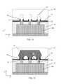
- a contact hole 90is formed in the second interlayer dielectric layer 85 and the insulating layer 80 so as to expose the epitaxial source and drain structures 60 with the silicide layer 70 , as shown in FIG. 11 .
- the contact plug 100may include a single layer or multiple layers of any suitable metal such as Co, W, Ti, Ta, Cu, Al and/or Ni and/or nitride thereof.
- CMOS processesare performed to form various features such as additional interlayer dielectric layer, contacts/vias, interconnect metal layers, and passivation layers, etc.
- the silicide layer 70is formed after the contact hole 90 is opened.
- the metal gate structures, the insulating layer 80 (contact etching stop layer) and the interlayer dielectric layer 85are formed, without forming a silicide layer.
- a contact holeis formed in the insulating layer 80 and the interlayer dielectric layer 85 to expose the upper surface of the epitaxial source/drain structure 60 , and then a silicide layer is formed on the upper surface of the epitaxial source/drain structure 60 .
- the conductive materialis formed in the contact hole, thereby forming a contact plug.
- FIGS. 13 and 14show exemplary cross sectional views of various stages for manufacturing a Fin FET device according to another embodiment of the present disclosure.
- the height H 3 of the sleeve-like portions 55is in a range from about 1 nm to about 10 nm in some embodiments.
- the epitaxial source/drain structure 60is formed, thereby forming voids 65 ′, as shown in FIG. 14 .
- the height H 4 of the voids 65 ′ in this embodimentis greater than the height H 2 in FIG. 8 .
- the height H 4is in a range from about 20 nm to about 35 nm in some embodiments.
- a parasitic capacitance at the source/drain structurecan be reduced. Further, by letting the fin mask layer (e.g., SiN) remain on the upper surface of the isolation insulating layer, the height (dimension) of the void can be larger.
- the fin mask layere.g., SiN
- a first fin structure and a second fin structureare formed over a substrate.
- the first and second fin structuresextend in a first direction in plan view.
- An isolation insulating layeris formed over the substrate so that lower portions of the first and second fin structures are embedded in the isolation insulating layer and upper portions of the first and second fin structures are exposed from the isolation insulating layer.
- a gate structureis formed over parts of the first and second fin structures.
- the gate structureincludes a gate pattern, a dielectric layer disposed between the gate pattern and the first and second fin structures, and a cap insulating layer disposed over the gate pattern.
- the gate structureextends in a second direction crossing the first direction in plan view.
- a fin mask layeris formed on sidewalls of the first and second fin structures protruding from the isolation insulating layer and not covered by the gate structure, and on an upper surface of the isolation insulating layer. Upper portions of the first and second fin structures are recessed. A first epitaxial source/drain structure is formed over the recessed first fin structure, and a second epitaxial source/drain structure is formed over the recessed second fin structure. In the recessing upper portions of the first and second fin structures, the fin mask layer disposed on the sidewalls of the first and second fin structures are removed, while the fin mask layer disposed on the upper surface of the isolation insulating layer remains. The first and second epitaxial source/drain structures are merged such that a void is formed between the merged first and second epitaxial source/drain structures and the remaining fin mask layer on the upper surface of the isolation insulating layer.
- a first fin structure and a second fin structureare formed over a substrate.
- the first and second fin structuresextend in a first direction in plan view.
- An isolation insulating layeris formed over the substrate so that lower portions of the first and second fin structures are embedded in the isolation insulating layer and upper portions of the first and second fin structures are exposed from the isolation insulating layer.
- a gate structureis formed over parts of the first and second fin structures.
- the gate structureincludes a gate pattern, a dielectric layer disposed between the gate pattern and the first and second fin structures, a cap insulating layer disposed over the gate pattern.
- the gate structureextends in a second direction crossing the first direction in plan view.
- a fin mask layeris formed on sidewalls of the first and second fin structures protruding from the isolation insulating layer and not covered by the gate structure, and on an upper surface of the isolation insulating layer. Upper portions of the first and second fin structures are recessed. A first epitaxial source/drain structure is formed over the recessed first fin structure, and a second epitaxial source/drain structure is formed over the recessed second fin structure. In the recessing upper portions of the first and second fin structures, a lower portion of the fin mask layer disposed on the sidewalls of the first and second fin structures and the fin mask layer disposed on the upper surface of the isolation insulating layer remain. The first and second epitaxial source/drain structures are merged such that a void is formed between the merged first and second epitaxial source/drain structures and the remaining fin mask layer on the upper surface of the isolation insulating layer.
- a semiconductor deviceincludes an isolation insulating layer, a first fin structure and a second fin structure, a gate structure, a source/drain structure and a dielectric layer.
- the isolation insulating layeris disposed over a substrate.
- the first fin structure and the second fin structureare both disposed over the substrate, and extend in a first direction in plan view.
- the gate structureis disposed over parts of the first and second fin structures, and extends in a second direction crossing the first direction.
- the dielectric layeris disposed on an upper surface of the isolation insulating layer.
- the first and second fin structures not covered by the gate structureare recessed below the upper surface of the isolation insulating layer.
- the source/drain structureis formed over the recessed first and second fin structures. A void is formed between the source/drain structure and the dielectric layer.
Landscapes
- Engineering & Computer Science (AREA)
- Physics & Mathematics (AREA)
- Condensed Matter Physics & Semiconductors (AREA)
- General Physics & Mathematics (AREA)
- Manufacturing & Machinery (AREA)
- Computer Hardware Design (AREA)
- Microelectronics & Electronic Packaging (AREA)
- Power Engineering (AREA)
- Insulated Gate Type Field-Effect Transistor (AREA)
- Chemical & Material Sciences (AREA)
- Materials Engineering (AREA)
Abstract
Description
- This application is a Divisional Application of U.S. Ser. No. 15/061,609, filed Mar. 4, 2016, the entire content of which application is incorporated herein by reference.
- The disclosure relates to a semiconductor integrated circuit, and more particularly to a semiconductor device having an epitaxial source/drain (S/D) structure with voids and its manufacturing process.
- As the semiconductor industry has progressed into nanometer technology process nodes in pursuit of higher device density, higher performance, and lower costs, challenges from both fabrication and design issues have resulted in the development of three-dimensional designs, such as a fin field effect transistor (Fin FET) and the use of a metal gate structure with a high-k (dielectric constant) material. The metal gate structure is often manufactured by using gate replacement technologies, and sources and drains are formed by using an epitaxial growth method.
- The present disclosure is best understood from the following detailed description when read with the accompanying figures. It is emphasized that, in accordance with the standard practice in the industry, various features are not drawn to scale and are used for illustration purposes only. In fact, the dimensions of the various features may be arbitrarily increased or reduced for clarity of discussion.
FIGS. 1-12 show exemplary cross sectional views of various stages for manufacturing a Fin FET device according to one embodiment of the present disclosure.FIGS. 13 and 14 show exemplary cross sectional views of various stages for manufacturing a Fin FET device according to another embodiment of the present disclosure- It is to be understood that the following disclosure provides many different embodiments, or examples, for implementing different features of the invention. Specific embodiments or examples of components and arrangements are described below to simplify the present disclosure. These are, of course, merely examples and are not intended to be limiting. For example, dimensions of elements are not limited to the disclosed range or values, but may depend upon process conditions and/or desired properties of the device. Moreover, the formation of a first feature over or on a second feature in the description that follows may include embodiments in which the first and second features are formed in direct contact, and may also include embodiments in which additional features may be formed interposing the first and second features, such that the first and second features may not be in direct contact. Various features may be arbitrarily drawn in different scales for simplicity and clarity. In the accompanied drawings, some layers/features may be omitted for simplification.
- Further, spatially relative terms, such as “beneath,” “below,” “lower,” “above,” “upper” and the like, may be used herein for ease of description to describe one element or feature's relationship to another element(s) or feature(s) as illustrated in the figures. The spatially relative terms are intended to encompass different orientations of the device in use or operation in addition to the orientation depicted in the figures. The apparatus may be otherwise oriented (rotated 90 degrees or at other orientations) and the spatially relative descriptors used herein may likewise be interpreted accordingly. In addition, the term “made of” may mean either “comprising” or “consisting of.” Further, in the following fabrication process, there may be one or more additional operations in/between the described operations, and the order of operations may be changed.
FIGS. 1-12 show exemplary cross sectional views of various stages for manufacturing a Fin FET device according to one embodiment of the present disclosure. It is understood that additional operations can be provided before, during, and after processes shown byFIGS. 1-12 , and some of the operations described below can be replaced or eliminated, for additional embodiments of the method. The order of the operations/processes may be interchangeable.- A
mask layer 15 is formed over asubstrate 10. Themask layer 15 is formed by, for example, a thermal oxidation process and/or a chemical vapor deposition (CVD) process. Thesubstrate 10 is, for example, a p-type silicon or germanium substrate with an impurity concentration in a range from about 1×1015cm−3to about 1×1016cm−3. In other embodiments, the substrate is an n-type silicon or germanium substrate with an impurity concentration in a range from about 1×1015cm−3to about 1×1016cm−3. - Alternatively, the
substrate 10 may comprise another elementary semiconductor, such as germanium; a compound semiconductor including IV-IV compound semiconductors such as SiC and SiGe, III-V compound semiconductors such as GaAs, GaP, GaN, InP, InAs, InSb, GaAsP, AlGaN, AlInAs, AlGaAs, GaInAs, GaInP, and/or GaInAsP; or combinations thereof. In one embodiment, thesubstrate 10 is a silicon layer of an SOI (silicon-on insulator) substrate. When an SOI substrate is used, the fin structure may protrude from the silicon layer of the SOI substrate or may protrude from the insulator layer of the SOI substrate. In the latter case, the silicon layer of the SOI substrate is used to form the fin structure. Amorphous substrates, such as amorphous Si or amorphous SiC, or insulating material, such as silicon oxide may also be used as thesubstrate 10. Thesubstrate 10 may include various regions that have been suitably doped with impurities (e.g., p-type or n-type conductivity). - The
mask layer 15 includes, for example, a pad oxide (e.g., silicon oxide)layer 15A and a siliconnitride mask layer 15B in some embodiments. - The
pad oxide layer 15A may be formed by using thermal oxidation or a CVD process. The siliconnitride mask layer 15B may be formed by a physical vapor deposition (PVD), such as a sputtering method, a CVD, plasma-enhanced chemical vapor deposition (PECVD), an atmospheric pressure chemical vapor deposition (APCVD), a low-pressure CVD (LPCVD), a high density plasma CVD (HDPCVD), an atomic layer deposition (ALD), and/or other processes. - The thickness of the
pad oxide layer 15A is in a range from about 2 nm to about 15 nm and the thickness of the siliconnitride mask layer 15B is in a range from about 2 nm to about 50 nm in some embodiments. A mask pattern is further formed over the mask layer. The mask pattern is, for example, a resist pattern formed by lithography operations. - By using the mask pattern as an etching mask, a
hard mask pattern 15 of the pad oxide layer and the silicon nitride mask layer is formed, as shown inFIG. 1 . - Then, as shown in
FIG. 2 , by using thehard mask pattern 15 as an etching mask, thesubstrate 10 is patterned intofin structures 20 by trench etching using a dry etching method and/or a wet etching method. - In
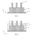
FIG. 2 , threefin structures 20 are disposed over thesubstrate 10. However, the number of the fin structures is not limited to three. The numbers may be as small as one or more than three. In addition, one or more dummy fin structures may be disposed adjacent both sides of thefin structure 20 to improve pattern fidelity in patterning processes. - The
fin structure 20 may be made of the same material as thesubstrate 10 and may continuously extend from thesubstrate 10. In this embodiment, the fin structure is made of Si. The silicon layer of thefin structure 20 may be intrinsic, or appropriately doped with an n-type impurity or a p-type impurity. - The width W1 of the
fin structure 20 is in a range from about 5 nm to about 40 nm in some embodiments, and is in a range from about 7 nm to about 12 nm in other embodiments. The space S1 between two fin structures is in a range from about 10 nm to about 50 nm in some embodiments. The height (along the Z direction) of thefin structure 20 is in a range from about 100 nm to about 300 nm in some embodiments, and is in a range from about 50 nm to 100 nm in other embodiments. - The lower part of the
fin structure 20 under the gate structure40 (see,FIG. 5A ) may be referred to as a well region, and the upper part of thefin structure 20 may be referred to as a channel region. Under thegate structure 40, the well region is embedded in the isolation insulating layer30 (see,FIG. 5A ), and the channel region protrudes from theisolation insulating layer 30. A lower part of the channel region may also be embedded in theisolation insulating layer 30 to a depth of about 1 nm to about 5 nm. - The height of the well region is in a range from about 60 nm to 100 nm in some embodiments, and the height of the channel region is in a range from about 40 nm to 60 nm, and is in a range from about 38 nm to about 55 nm in other embodiments.
- After the
fin structures 20 are formed, thesubstrate 10 is further etched to form amesa shape 10M, as shown inFIG. 3 . In other embodiments, themesa shape 10M is first formed, and then thefin structures 20 are formed. - After the
fin structures 20 and themesa shape 10M are formed, theisolation insulating layer 30 is formed in spaces between the fin structures and/or a space between one fin structure and another element formed over thesubstrate 10. Theisolation insulating layer 30 may also be called a “shallow-trench-isolation (STI)” layer. The insulating material for theisolation insulating layer 30 may include one or more layers of silicon oxide, silicon nitride, silicon oxynitride (SiON), SiOCN, fluorine-doped silicate glass (FSG), or a low-k dielectric material. The isolation insulating layer is formed by LPCVD (low pressure chemical vapor deposition), plasma-CVD or flowable CVD. In the flowable CVD, flowable dielectric materials instead of silicon oxide may be deposited. Flowable dielectric materials, as their name suggest, can “flow” during deposition to fill gaps or spaces with a high aspect ratio. Usually, various chemistries are added to silicon-containing precursors to allow the deposited film to flow. In some embodiments, nitrogen hydride bonds are added. Examples of flowable dielectric precursors, particularly flowable silicon oxide precursors, include a silicate, a siloxane, a methyl silsesquioxane (MSQ), a hydrogen silsesquioxane (HSQ), an MSQ/HSQ, a perhydrosilazane (TCPS), a perhydro-polysilazane (PSZ), a tetraethyl orthosilicate (TEOS), or a silyl-amine, such as trisilylamine (TSA). These flowable silicon oxide materials are formed in a multiple-operation process. After the flowable film is deposited, it is cured and then annealed to remove un-desired element(s) to form silicon oxide. When the un-desired element(s) is removed, the flowable film densifies and shrinks. In some embodiments, multiple anneal processes are conducted. The flowable film is cured and annealed more than once. The flowable film may be doped with boron and/or phosphorous. - The insulating
layer 30 is first formed in a thick layer so that the fin structures are embedded in the thick layer, and the thick layer is recessed so as to expose the upper portions of thefin structures 20, as shown inFIG. 4 . The height H1 of the fin structures from the upper surface of theisolation insulating layer 30 is in a range from about 20 nm to about 100 nm in some embodiments, and is in a range from about 30 nm to about 50 nm in other embodiments. After or before recessing theisolation insulating layer 30, a thermal process, for example, an anneal process, may be performed to improve the quality of theisolation insulating layer 30. In certain embodiments, the thermal process is performed by using rapid thermal annealing (RTA) at a temperature in a range from about 900° C. to about 1050° C. for about 1.5 seconds to about 10 seconds in an inert gas ambient, such as an N2, Ar or He ambient. - After the insulating
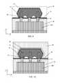
layer 30 is formed, agate structure 40 is formed over thefin structures 20, as shown inFIGS. 5A-5C .FIG. 5A is an exemplary perspective view,FIG. 5B is an exemplary cross sectional view along line a-a ofFIG. 5A andFIG. 5C is an exemplary cross sectional view along line b-b ofFIG. 5A .FIGS. 6-14 are also exemplary cross sectional views along line b-b ofFIG. 5A . - As shown in
FIG. 5A , thegate structure 40 extends in the X direction, while thefin structures 20 extend in the Y direction. - To fabricate the
gate structure 40, a dielectric layer and a poly silicon layer are formed over theisolation insulating layer 30 and the exposedfin structures 20, and then patterning operations are performed so as to obtain gate structures including agate pattern 44 made of poly silicon and adielectric layer 42. In some embodiments, the polysilicon layer is patterned by using a hard mask and the hard mask remains on thegate pattern 44 as acap insulating layer 46. The hard mask (cap insulating layer46) includes one or more layers of insulating material. Thecap insulating layer 46 includes a silicon nitride layer formed over a silicon oxide layer in some embodiments. In other embodiments, thecap insulating layer 46 includes a silicon oxide layer formed over a silicon nitride layer. The insulating material for thecap insulating layer 46 may be formed by CVD, PVD, ALD, e-beam evaporation, or other suitable process. In some embodiments, thedielectric layer 42 may include one or more layers of silicon oxide, silicon nitride, silicon oxy-nitride, or high-k dielectrics. In some embodiments, a thickness of thedielectric layer 42 is in a range from about 2 nm to about 20 nm, and in a range from about 2 nm to about 10 nm in other embodiments. The height H2 of the gate structures is in a range from about 50 nm to about 400 nm in some embodiments, and is in a range from about 100 nm to 200 nm in other embodiments. - In some embodiments, a gate replacement technology is employed. In such a case, the
gate pattern 44 and thedielectric layer 42 are a dummy gate electrode and a dummy gate dielectric layer, respectively, which are subsequently removed. If a gate-first technology is employed, thegate pattern 44 and thedielectric layer 42 are used as a gate electrode and a gate dielectric layer. - Further,
gate sidewall spacers 48 are formed on both sidewalls of the gate pattern. The sidewall spacers48 include one or more layers of insulating material, such as SiO2, SiN, SiON, SiOCN or SiCN, which are formed by CVD, PVD, ALD, e-beam evaporation, or other suitable process. A low-k dielectric material may be used as the sidewall spacers. The sidewall spacers48 are formed by forming a blanket layer of insulating material and performing anisotropic etching. In one embodiment, the sidewall spacer layers are made of silicon nitride based material, such as SiN, SiON, SiOCN or SiCN. - Then, as shown in
FIG. 6 , afin mask layer 50 is formed over thefin structures 20. Thefin mask layer 50 is made of dielectric material including silicon nitride based material, such as SiN, SiON, SiOCN or SiCN. In one embodiment, SiN is used as thefin mask layer 50. Thefin mask layer 50 is formed by CVD, PVD, ALD, e-beam evaporation, or other suitable process. The thickness of thefin mask layer 50 is in a range from about 30 nm to about 70 nm in some embodiments. - In some embodiments, the
fin mask layer 50 and thesidewall spacers 48 for the gate structure are separately formed. In other embodiments, the same blanket layer is used for thefin mask layer 50 and thesidewall spacers 48. - After forming the
fin mask layer 50, the upper portion of thefin structures 20 are recessed and a part of thefin mask layer 50 disposed on side surfaces and the top surface of the fin structures protruding from the isolation insulating layer are removed by a dry etching and/or a wet etching operation. The upper portion of thefin structures 20 are recessed (etched) down to the level equal to or below the upper surface of thefin mask layer 50 on the upper surfaceisolation insulating layer 30, as shown inFIG. 7 . By adjusting etching conditions, for example, an over-etching time, thefin mask layer 50 remains on the upper surface of theisolation insulating layer 30. The thickness of the remainingfin mask layer 50 is in a range from about 2 nm to about 10 nm in some embodiments. - Then, as shown in
FIG. 8 , an epitaxial source/drain structure 60 is formed over the recessedfin structures 20. The epitaxial source/drain structure 60 is made of one or more layers of semiconductor material having a different lattice constant than the fin structures20 (channel regions). When the fin structures are made of Si, the epitaxial source/drain structure 60 includes SiP, SiC or SiCP for an n-channel Fin FET and SiGe or Ge for a p-channel Fin FET. The epitaxial source/drain structure 60 is epitaxially formed over the upper portions of the recessed fin structures. Due to the crystal orientation of the substrate formed into the fin structures20 (e.g., (100) plane), the epitaxial source/drain structure 60 grows laterally and have a diamond-like shape. - The source/
drain epitaxial layer 60 may be grown at a temperature of about 600 to 800° C. under a pressure of about 80 to 150 Torr, by using a Si containing gas such as SiH4, Si2H6or SiCl2H2, a Ge containing gas, such as GeH4, Ge2H6or GeCl2H2, a C containing gas, such as CH4or C2H6, and/or a dopant gas, such as PH3. The source/drain structure for an n-channel FET and the source/drain structure for a p-channel FET may be formed by separate epitaxial processes. - Due to the relatively small space between the fin structures and the
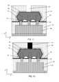
fin mask layer 50 remaining on the upper surface of the isolation insulating layer between the fin structures, the adjacent epitaxial source/drain structures formed over each of thefirst fin structures 20 are merged such that a void or a gap (an air gap)65 is formed by the merged second epitaxial source/drain structure 60 and thefin mask layer 50 on the upper surface of theisolation insulating layer 30, as shown inFIG. 8 . - In particular, due to the
fin mask layer 50 on the upper surface of theisolation insulating layer 30, the height H2 of the void65 is larger than the case where nofin mask layer 50 remains on the upper surface of theisolation insulating layer 30. In some embodiments, the height H2 of the void is in a range from about 10 nm to about 30 nm measured from the upper surface offin mask layer 50, and in a range from about 15 nm to about 25 nm in other embodiments. In addition, due to the remainingfin mask layer 50, theisolation insulting layer 30 is protected during the fin etching. - After the epitaxial source/
drain structure 60 is formed, as shown inFIG. 9 , asilicide layer 70 is formed over the epitaxial source/drain structure 60. - A metal material, such as Ni, Ti, Ta and/or W, is formed over the epitaxial source/
drain structure 60, and an annealing operation is performed to form asilicide layer 70. In other embodiments, a silicide material, such as NiSi, TiSi, TaSi and/or WSi, is formed over the epitaxial source/drain structure 60, and an annealing operation may be performed. The annealing operation is performed at a temperature of about 250° C. to about 850° C. The metal material or the silicide material is formed by CVD or ALD. The thickness of thesilicide layer 70 is in a range from about 4 nm to about 10 nm in some embodiments. Before or after the annealing operations, the metal material or the silicide material formed over theisolation insulating layer 30 is selectively removed. - Then, a metal gate structure (not shown) is formed. After forming the
silicide layer 70, the dummy gate structures (dummy gate electrode 44 and dummy gate dielectric layer42) are removed and replaced with a metal gate structures (metal gate electrode and gate dielectric layer). - In certain embodiments, a first interlayer dielectric layer is formed over the dummy gate structures and a planarization operation, such as a chemical mechanical polishing (CMP) process or an etch-back process, is performed to expose the upper surface of the
dummy gate electrode 44. Then, thedummy gate electrode 44 and the dummygate dielectric layer 42 are removed, by appropriate etching processes, respectively, to form a gate opening. Metal gate structures including a gate dielectric layer and metal gate electrode are formed in the gate openings. - The gate dielectric layer may be formed over an interface layer (not shown) disposed over the channel layer of the
fin structures 20. The interface layer may include silicon oxide or germanium oxide with a thickness of 0.2 nm to 1.5 nm in some embodiments. In other embodiments, the thickness of the interface layer is in a range about 0.5 nm to about 1.0 nm. - The gate dielectric layer includes one or more layers of dielectric materials, such as silicon oxide, silicon nitride, or high-k dielectric material, other suitable dielectric material, and/or combinations thereof. Examples of high-k dielectric material include HfO2, HfSiO, HfSiON, HfTaO, HfTiO, HfZrO, zirconium oxide, aluminum oxide, titanium oxide, hafnium dioxide-alumina (HfO2—Al2O3) alloy, other suitable high-k dielectric materials, and/or combinations thereof. The gate dielectric layer is formed by, for example, chemical vapor deposition (CVD), physical vapor deposition (PVD), atomic layer deposition (ALD), high density plasma CVD (HDPCVD), or other suitable methods, and/or combinations thereof. The thickness of the gate dielectric layer is in a range from about 1 nm to about 10 nm in some embodiments, and may be in a range from about 2 nm to about 7 nm in other embodiments.
- The metal gate electrode is formed over the gate dielectric layer. The metal gate electrode includes one or more layers of any suitable metal material, such as aluminum, copper, titanium, tantalum, cobalt, molybdenum, tantalum nitride, nickel silicide, cobalt silicide, TiN, WN, TiAl, TiAlN, TaCN, TaC, TaSiN, metal alloys, other suitable materials, and/or combinations thereof.
- In certain embodiments of the present disclosure, one or more work function adjustment layers (not shown) may be interposed between the gate dielectric layer and the metal gate electrode. The work function adjustment layer is made of a conductive material such as a single layer of TiN, TaN, TaAlC, TiC, TaC, Co, Al, TiAl, HfTi, TiSi, TaSi or TiAlC, or a multilayer of two or more of these materials. For the n-channel Fin FET, one or more of TaN, TaAlC, TiN, TiC, Co, TiAl, HfTi, TiSi and TaSi is used as the work function adjustment layer, and for the p-channel Fin FET, one or more of TiAlC, Al, TiAl, TaN, TaAlC, TiN, TiC and Co is used as the work function adjustment layer.
- After depositing appropriate materials for the metal gate structures, planarization operations, such as CMP, are performed.
- Then, as shown in
FIG. 10 , an insulatinglayer 80, functioning as a contact etching stop layer, is formed over the formed metal gate structure and the source/drain structures 60, and then the secondinterlayer dielectric layer 85 is formed. The insulatinglayer 80 is one or more layers of insulating material. In one embodiment, the insulatinglayer 80 is made of silicon nitride formed by CVD. - By using a patterning operation including lithography, a
contact hole 90 is formed in the secondinterlayer dielectric layer 85 and the insulatinglayer 80 so as to expose the epitaxial source and drainstructures 60 with thesilicide layer 70, as shown inFIG. 11 . - Then, the contact hole is filled with a conductive material, thereby forming a
contact plug 100, as shown inFIG. 12 . Thecontact plug 100 may include a single layer or multiple layers of any suitable metal such as Co, W, Ti, Ta, Cu, Al and/or Ni and/or nitride thereof. - After forming the contact plug, further CMOS processes are performed to form various features such as additional interlayer dielectric layer, contacts/vias, interconnect metal layers, and passivation layers, etc.
- In the alternative, the
silicide layer 70 is formed after thecontact hole 90 is opened. In such a case, after forming the epitaxial source/drain structure 60 as shown inFIG. 8 , the metal gate structures, the insulating layer80 (contact etching stop layer) and theinterlayer dielectric layer 85 are formed, without forming a silicide layer. Then, a contact hole is formed in the insulatinglayer 80 and theinterlayer dielectric layer 85 to expose the upper surface of the epitaxial source/drain structure 60, and then a silicide layer is formed on the upper surface of the epitaxial source/drain structure 60. After forming the silicide layer, the conductive material is formed in the contact hole, thereby forming a contact plug. FIGS. 13 and 14 show exemplary cross sectional views of various stages for manufacturing a Fin FET device according to another embodiment of the present disclosure.- During the recess etching of the
fin mask layer 50 and thefin structures 20 described with respect toFIG. 7 , some lower portions of thefin mask layer 50 disposed on sidewall of thefin structures 20 remain without being etched away thereby forming sleeve-like portions 55, as show inFIG. 13 . The height H3 of the sleeve-like portions 55 is in a range from about 1 nm to about 10 nm in some embodiments. - Then, similar to
FIG. 8 , the epitaxial source/drain structure 60 is formed, thereby formingvoids 65′, as shown inFIG. 14 . Due to the sleeve-like portions 55, the height H4 of thevoids 65′ in this embodiment is greater than the height H2 inFIG. 8 . The height H4 is in a range from about 20 nm to about 35 nm in some embodiments. - In the present disclosure, since a void is formed between the source/drain epitaxial layer and the isolation insulting layer (STI), a parasitic capacitance at the source/drain structure can be reduced. Further, by letting the fin mask layer (e.g., SiN) remain on the upper surface of the isolation insulating layer, the height (dimension) of the void can be larger.
- It will be understood that not all advantages have been necessarily discussed herein, no particular advantage is required for all embodiments or examples, and other embodiments or examples may offer different advantages.
- In accordance with one aspect of the present disclosure, in a method of manufacturing a semiconductor device including a Fin FET, a first fin structure and a second fin structure are formed over a substrate. The first and second fin structures extend in a first direction in plan view. An isolation insulating layer is formed over the substrate so that lower portions of the first and second fin structures are embedded in the isolation insulating layer and upper portions of the first and second fin structures are exposed from the isolation insulating layer. A gate structure is formed over parts of the first and second fin structures. The gate structure includes a gate pattern, a dielectric layer disposed between the gate pattern and the first and second fin structures, and a cap insulating layer disposed over the gate pattern. The gate structure extends in a second direction crossing the first direction in plan view. A fin mask layer is formed on sidewalls of the first and second fin structures protruding from the isolation insulating layer and not covered by the gate structure, and on an upper surface of the isolation insulating layer. Upper portions of the first and second fin structures are recessed. A first epitaxial source/drain structure is formed over the recessed first fin structure, and a second epitaxial source/drain structure is formed over the recessed second fin structure. In the recessing upper portions of the first and second fin structures, the fin mask layer disposed on the sidewalls of the first and second fin structures are removed, while the fin mask layer disposed on the upper surface of the isolation insulating layer remains. The first and second epitaxial source/drain structures are merged such that a void is formed between the merged first and second epitaxial source/drain structures and the remaining fin mask layer on the upper surface of the isolation insulating layer.
- In accordance with another aspect of the present disclosure, in a method of manufacturing a semiconductor device including a Fin FET, a first fin structure and a second fin structure are formed over a substrate. The first and second fin structures extend in a first direction in plan view. An isolation insulating layer is formed over the substrate so that lower portions of the first and second fin structures are embedded in the isolation insulating layer and upper portions of the first and second fin structures are exposed from the isolation insulating layer. A gate structure is formed over parts of the first and second fin structures. The gate structure includes a gate pattern, a dielectric layer disposed between the gate pattern and the first and second fin structures, a cap insulating layer disposed over the gate pattern. The gate structure extends in a second direction crossing the first direction in plan view. A fin mask layer is formed on sidewalls of the first and second fin structures protruding from the isolation insulating layer and not covered by the gate structure, and on an upper surface of the isolation insulating layer. Upper portions of the first and second fin structures are recessed. A first epitaxial source/drain structure is formed over the recessed first fin structure, and a second epitaxial source/drain structure is formed over the recessed second fin structure. In the recessing upper portions of the first and second fin structures, a lower portion of the fin mask layer disposed on the sidewalls of the first and second fin structures and the fin mask layer disposed on the upper surface of the isolation insulating layer remain. The first and second epitaxial source/drain structures are merged such that a void is formed between the merged first and second epitaxial source/drain structures and the remaining fin mask layer on the upper surface of the isolation insulating layer.
- In accordance with another aspect of the present disclosure, a semiconductor device includes an isolation insulating layer, a first fin structure and a second fin structure, a gate structure, a source/drain structure and a dielectric layer. The isolation insulating layer is disposed over a substrate. The first fin structure and the second fin structure are both disposed over the substrate, and extend in a first direction in plan view. The gate structure is disposed over parts of the first and second fin structures, and extends in a second direction crossing the first direction. The dielectric layer is disposed on an upper surface of the isolation insulating layer. The first and second fin structures not covered by the gate structure are recessed below the upper surface of the isolation insulating layer. The source/drain structure is formed over the recessed first and second fin structures. A void is formed between the source/drain structure and the dielectric layer.
- The foregoing outlines features of several embodiments or examples so that those skilled in the art may better understand the aspects of the present disclosure. Those skilled in the art should appreciate that they may readily use the present disclosure as a basis for designing or modifying other processes and structures for carrying out the same purposes and/or achieving the same advantages of the embodiments or examples introduced herein. Those skilled in the art should also realize that such equivalent constructions do not depart from the spirit and scope of the present disclosure, and that they may make various changes, substitutions, and alterations herein without departing from the spirit and scope of the present disclosure.
Claims (20)
Priority Applications (2)
| Application Number | Priority Date | Filing Date | Title |
|---|---|---|---|
| US15/830,859US11107734B2 (en) | 2016-03-04 | 2017-12-04 | Semiconductor device and manufacturing method thereof |
| US16/585,859US20200027793A1 (en) | 2016-03-04 | 2019-09-27 | Semiconductor device and manufacturing method thereof |
Applications Claiming Priority (2)
| Application Number | Priority Date | Filing Date | Title |
|---|---|---|---|
| US15/061,609US9865504B2 (en) | 2016-03-04 | 2016-03-04 | Semiconductor device and manufacturing method thereof |
| US15/830,859US11107734B2 (en) | 2016-03-04 | 2017-12-04 | Semiconductor device and manufacturing method thereof |
Related Parent Applications (1)
| Application Number | Title | Priority Date | Filing Date |
|---|---|---|---|
| US15/061,609DivisionUS9865504B2 (en) | 2016-03-04 | 2016-03-04 | Semiconductor device and manufacturing method thereof |
Related Child Applications (1)
| Application Number | Title | Priority Date | Filing Date |
|---|---|---|---|
| US16/585,859DivisionUS20200027793A1 (en) | 2016-03-04 | 2019-09-27 | Semiconductor device and manufacturing method thereof |
Publications (2)
| Publication Number | Publication Date |
|---|---|
| US20180102292A1true US20180102292A1 (en) | 2018-04-12 |
| US11107734B2 US11107734B2 (en) | 2021-08-31 |
Family
ID=59367450
Family Applications (3)
| Application Number | Title | Priority Date | Filing Date |
|---|---|---|---|
| US15/061,609ActiveUS9865504B2 (en) | 2016-03-04 | 2016-03-04 | Semiconductor device and manufacturing method thereof |
| US15/830,859ActiveUS11107734B2 (en) | 2016-03-04 | 2017-12-04 | Semiconductor device and manufacturing method thereof |
| US16/585,859PendingUS20200027793A1 (en) | 2016-03-04 | 2019-09-27 | Semiconductor device and manufacturing method thereof |
Family Applications Before (1)
| Application Number | Title | Priority Date | Filing Date |
|---|---|---|---|
| US15/061,609ActiveUS9865504B2 (en) | 2016-03-04 | 2016-03-04 | Semiconductor device and manufacturing method thereof |
Family Applications After (1)
| Application Number | Title | Priority Date | Filing Date |
|---|---|---|---|
| US16/585,859PendingUS20200027793A1 (en) | 2016-03-04 | 2019-09-27 | Semiconductor device and manufacturing method thereof |
Country Status (4)
| Country | Link |
|---|---|
| US (3) | US9865504B2 (en) |
| KR (2) | KR20170103612A (en) |
| CN (1) | CN107154384B (en) |
| TW (1) | TWI582998B (en) |
Families Citing this family (31)
| Publication number | Priority date | Publication date | Assignee | Title |
|---|---|---|---|---|
| CN105977299B (en)* | 2016-06-17 | 2019-12-10 | 中国科学院微电子研究所 | Semiconductor device and method for manufacturing the same |
| US10157918B2 (en)* | 2016-08-03 | 2018-12-18 | Taiwan Semiconductor Manufacturing Company, Ltd. | Semiconductor device and method |
| KR102318560B1 (en)* | 2017-04-12 | 2021-11-01 | 삼성전자주식회사 | Semiconductor device |
| KR102519551B1 (en) | 2017-08-03 | 2023-04-10 | 삼성전자주식회사 | Semiconductor device |
| US10141231B1 (en)* | 2017-08-28 | 2018-11-27 | Taiwan Semiconductor Manufacturing Co., Ltd. | FinFET device with wrapped-around epitaxial structure and manufacturing method thereof |
| KR102337408B1 (en)* | 2017-09-13 | 2021-12-10 | 삼성전자주식회사 | Semiconductor devices having a vertical channel and method of manufacturing the same |
| US10347720B2 (en) | 2017-10-30 | 2019-07-09 | Taiwan Semiconductor Manufacturing Co., Ltd. | Doping for semiconductor device with conductive feature |
| US10770354B2 (en)* | 2017-11-15 | 2020-09-08 | Taiwan Semiconductor Manufacturing Co., Ltd. | Method of forming integrated circuit with low-k sidewall spacers for gate stacks |
| KR20230006054A (en)* | 2017-11-30 | 2023-01-10 | 인텔 코포레이션 | Fin patterning for advanced integrated circuit structure fabrication |
| KR102492300B1 (en)* | 2017-12-07 | 2023-01-27 | 삼성전자주식회사 | Semiconductor device |
| US10720494B2 (en)* | 2018-01-22 | 2020-07-21 | Globalfoundries Inc. | Field-effect transistors with airgaps |
| KR102574320B1 (en)* | 2018-06-20 | 2023-09-04 | 삼성전자주식회사 | Semiconductor device including fin-FET |
| US10872892B2 (en) | 2018-06-29 | 2020-12-22 | Taiwan Semiconductor Manufacturing Co., Ltd. | Semiconductor device and manufacturing method thereof |
| US11222951B2 (en) | 2018-08-31 | 2022-01-11 | Taiwan Semiconductor Manufacturing Co., Ltd. | Epitaxial source/drain structure and method |
| US10943829B2 (en)* | 2018-10-23 | 2021-03-09 | Taiwan Semiconductor Manufacturing Company, Ltd. | Slot contacts and method forming same |
| US11189728B2 (en) | 2019-09-05 | 2021-11-30 | Taiwan Semiconductor Manufacturing Co., Ltd. | Method of manufacturing a semiconductor device and a semiconductor device |
| CN112635560B (en) | 2019-10-08 | 2023-12-05 | 联华电子股份有限公司 | Fin-shaped transistor structure and manufacturing method thereof |
| DE102020129004A1 (en)* | 2019-12-26 | 2021-07-01 | Taiwan Semiconductor Manufacturing Co., Ltd. | SEMICONDUCTOR STRUCTURE WITH INSULATING ELEMENT AND PROCESS FOR MAKING IT |
| US11282944B2 (en) | 2019-12-30 | 2022-03-22 | Taiwan Semiconductor Manufacturing Co., Ltd. | Method of manufacturing a semiconductor device and a semiconductor device |
| KR102515293B1 (en)* | 2019-12-30 | 2023-03-29 | 타이완 세미콘덕터 매뉴팩쳐링 컴퍼니 리미티드 | Method of manufacturing a semiconductor device and a semiconductor device |
| US11522050B2 (en)* | 2020-01-30 | 2022-12-06 | Taiwan Semiconductor Manufacturing Co., Ltd. | Method of manufacturing a semiconductor device and a semiconductor device |
| DE102020132562B4 (en) | 2020-01-30 | 2024-02-22 | Taiwan Semiconductor Manufacturing Co., Ltd. | METHOD FOR PRODUCING A SEMICONDUCTOR DEVICE AND SEMICONDUCTOR DEVICE |
| US11862712B2 (en)* | 2020-02-19 | 2024-01-02 | Taiwan Semiconductor Manufacturing Co., Ltd. | Methods of semiconductor device fabrication including growing epitaxial features using different carrier gases |
| DE102021101473A1 (en)* | 2020-03-31 | 2021-09-30 | Taiwan Semiconductor Manufacturing Co., Ltd. | REDUCING PARASITARY CAPACITY IN FIELD EFFECT TRANSISTORS |
| US11387365B2 (en)* | 2020-04-01 | 2022-07-12 | Taiwan Semiconductor Manufacturing Co., Ltd. | Method of manufacturing a semiconductor device for recessed fin structure having rounded corners |
| DE102020126052A1 (en) | 2020-06-29 | 2021-12-30 | Taiwan Semiconductor Manufacturing Co., Ltd. | METHOD OF MANUFACTURING A SEMICONDUCTOR DEVICE AND A SEMICONDUCTOR DEVICE |
| US11489075B2 (en) | 2020-06-29 | 2022-11-01 | Taiwan Semiconductor Manufacturing Co., Ltd. | Method of manufacturing a semiconductor device and a semiconductor device |
| US11404561B2 (en)* | 2020-08-03 | 2022-08-02 | Taiwan Semiconductor Manufacturing Co., Ltd. | Semiconductor device and manufacturing method thereof |
| KR102837523B1 (en) | 2021-08-23 | 2025-07-22 | 삼성전자주식회사 | Semiconductor device |
| US12426300B2 (en)* | 2022-02-17 | 2025-09-23 | Taiwan Semiconductor Manufacturing Co., Ltd. | Transistor source/drain contacts and methods of forming the same |
| US12396220B2 (en) | 2022-08-02 | 2025-08-19 | Taiwan Semiconductor Manufacturing Company, Ltd. | Isolation structures in multi-gate field-effect transistors |
Citations (4)
| Publication number | Priority date | Publication date | Assignee | Title |
|---|---|---|---|---|
| US7300837B2 (en)* | 2004-04-30 | 2007-11-27 | Taiwan Semiconductor Manufacturing Co., Ltd | FinFET transistor device on SOI and method of fabrication |
| US20130249003A1 (en)* | 2012-03-21 | 2013-09-26 | Changwoo Oh | Field effect transistors including fin structures with different doped regions and semiconductor devices including the same |
| US9472669B1 (en)* | 2015-09-04 | 2016-10-18 | Taiwan Semiconductor Manufacturing Co., Ltd. | Semiconductor Fin FET device with epitaxial source/drain |
| US20160372596A1 (en)* | 2015-06-16 | 2016-12-22 | International Business Machines Corporation | LOW PARASITIC CAPACITANCE AND RESISTANCE finFET DEVICE |
Family Cites Families (47)
| Publication number | Priority date | Publication date | Assignee | Title |
|---|---|---|---|---|
| KR100487567B1 (en)* | 2003-07-24 | 2005-05-03 | 삼성전자주식회사 | Method for fabricating a finfet in a semiconductor device |
| US7939889B2 (en)* | 2007-10-16 | 2011-05-10 | Taiwan Semiconductor Manufacturing Company, Ltd. | Reducing resistance in source and drain regions of FinFETs |
| US7871873B2 (en) | 2009-03-27 | 2011-01-18 | Global Foundries Inc. | Method of forming fin structures using a sacrificial etch stop layer on bulk semiconductor material |
| US8653608B2 (en)* | 2009-10-27 | 2014-02-18 | Taiwan Semiconductor Manufacturing Company, Ltd. | FinFET design with reduced current crowding |
| US8426923B2 (en)* | 2009-12-02 | 2013-04-23 | Taiwan Semiconductor Manufacturing Company, Ltd. | Multiple-gate semiconductor device and method |
| US8263451B2 (en)* | 2010-02-26 | 2012-09-11 | Taiwan Semiconductor Manufacturing Company, Ltd. | Epitaxy profile engineering for FinFETs |
| US8487378B2 (en) | 2011-01-21 | 2013-07-16 | Taiwan Semiconductor Manufacturing Company, Ltd. | Non-uniform channel junction-less transistor |
| US8887106B2 (en) | 2011-12-28 | 2014-11-11 | Taiwan Semiconductor Manufacturing Company, Ltd. | Method of generating a bias-adjusted layout design of a conductive feature and method of generating a simulation model of a predefined fabrication process |
| US8759184B2 (en)* | 2012-01-09 | 2014-06-24 | Taiwan Semiconductor Manufacturing Company, Ltd. | FinFETs and the methods for forming the same |
| US9147765B2 (en)* | 2012-01-19 | 2015-09-29 | Globalfoundries Inc. | FinFET semiconductor devices with improved source/drain resistance and methods of making same |
| US9368388B2 (en) | 2012-04-13 | 2016-06-14 | Taiwan Semiconductor Manufacturing Company, Ltd. | Apparatus for FinFETs |
| US8691652B2 (en)* | 2012-05-03 | 2014-04-08 | United Microelectronics Corp. | Semiconductor process |
| US8729634B2 (en) | 2012-06-15 | 2014-05-20 | Taiwan Semiconductor Manufacturing Company, Ltd. | FinFET with high mobility and strain channel |
| US9142400B1 (en)* | 2012-07-17 | 2015-09-22 | Stc.Unm | Method of making a heteroepitaxial layer on a seed area |
| US8703556B2 (en) | 2012-08-30 | 2014-04-22 | Taiwan Semiconductor Manufacturing Company, Ltd. | Method of making a FinFET device |
| US8946029B2 (en)* | 2012-11-12 | 2015-02-03 | GlobalFoundries, Inc. | Methods of manufacturing integrated circuits having FinFET structures with epitaxially formed source/drain regions |
| US9147682B2 (en)* | 2013-01-14 | 2015-09-29 | Taiwan Semiconductor Manufacturing Company, Ltd. | Fin spacer protected source and drain regions in FinFETs |
| US8901607B2 (en) | 2013-01-14 | 2014-12-02 | Taiwan Semiconductor Manufacturing Company, Ltd. | Semiconductor device and fabricating the same |
| KR102049774B1 (en)* | 2013-01-24 | 2019-11-28 | 삼성전자 주식회사 | Semiconductor device and fabricated method thereof |
| US8921191B2 (en)* | 2013-02-05 | 2014-12-30 | GlobalFoundries, Inc. | Integrated circuits including FINFET devices with lower contact resistance and reduced parasitic capacitance and methods for fabricating the same |
| US8987791B2 (en) | 2013-02-27 | 2015-03-24 | Taiwan Semiconductor Manufacturing Company, Ltd. | FinFETs and methods for forming the same |
| US8826213B1 (en) | 2013-03-11 | 2014-09-02 | Taiwan Semiconductor Manufacturing Company, Ltd. | Parasitic capacitance extraction for FinFETs |
| US8943455B2 (en) | 2013-03-12 | 2015-01-27 | Taiwan Semiconductor Manufacturing Company, Ltd. | Methods for layout verification for polysilicon cell edge structures in FinFET standard cells |
| US8796093B1 (en)* | 2013-03-14 | 2014-08-05 | International Business Machines Corporation | Doping of FinFET structures |
| US8859379B2 (en)* | 2013-03-15 | 2014-10-14 | International Business Machines Corporation | Stress enhanced finFET devices |
| KR20150000546A (en)* | 2013-06-24 | 2015-01-05 | 삼성전자주식회사 | Semiconductor device and method for fabricating the same |
| KR102068980B1 (en)* | 2013-08-01 | 2020-01-22 | 삼성전자 주식회사 | Semiconductor device and method for fabricating the same |
| US20150076607A1 (en)* | 2013-09-18 | 2015-03-19 | International Business Machines Corporation | Fin field effect transistor with merged metal semiconductor alloy regions |
| US9391202B2 (en)* | 2013-09-24 | 2016-07-12 | Samsung Electronics Co., Ltd. | Semiconductor device |
| US9112033B2 (en)* | 2013-12-30 | 2015-08-18 | Taiwan Semiconductor Manufacturing Company, Ltd. | Source/drain structure of semiconductor device |
| US9391200B2 (en)* | 2014-06-18 | 2016-07-12 | Stmicroelectronics, Inc. | FinFETs having strained channels, and methods of fabricating finFETs having strained channels |
| KR20160005550A (en) | 2014-07-07 | 2016-01-15 | 삼성전자주식회사 | Semiconductor device |
| US9306067B2 (en)* | 2014-08-05 | 2016-04-05 | Taiwan Semiconductor Manufacturing Company, Ltd. | Nonplanar device and strain-generating channel dielectric |
| KR102150254B1 (en)* | 2014-09-15 | 2020-09-02 | 삼성전자주식회사 | Manufacturing method of semiconductor device |
| US9324713B1 (en)* | 2015-03-16 | 2016-04-26 | Globalfoundries Inc. | Eliminating field oxide loss prior to FinFET source/drain epitaxial growth |
| KR20160125208A (en)* | 2015-04-21 | 2016-10-31 | 삼성전자주식회사 | Semiconductor device having fin active regions and method of fabricating the same |
| DE102015006379B4 (en) | 2015-05-18 | 2022-03-17 | Azur Space Solar Power Gmbh | Scalable voltage source |
| KR20160136715A (en)* | 2015-05-20 | 2016-11-30 | 삼성전자주식회사 | Semiconductor devices and methods of manufacturing the same |
| US9953881B2 (en)* | 2015-07-20 | 2018-04-24 | Taiwan Semiconductor Manufacturing Company, Ltd. | Method of forming a FinFET device |
| US9755019B1 (en)* | 2016-03-03 | 2017-09-05 | Taiwan Semiconductor Manufacturing Co., Ltd. | Semiconductor device and manufacturing method thereof |
| US9812363B1 (en)* | 2016-11-29 | 2017-11-07 | Taiwan Semiconductor Manufacturing Company, Ltd. | FinFET device and method of forming same |
| US10707328B2 (en)* | 2016-11-30 | 2020-07-07 | Taiwan Semiconductor Manufacturing Co., Ltd. | Method of forming epitaxial fin structures of finFET |
| US9953875B1 (en)* | 2016-11-30 | 2018-04-24 | Taiwan Semiconductor Manufacturing Company | Contact resistance control in epitaxial structures of finFET |
| DE102017124779A1 (en)* | 2016-12-30 | 2018-07-05 | Taiwan Semiconductor Manufacturing Co., Ltd. | Semiconductor device and its manufacturing method |
| US11348840B2 (en)* | 2019-10-30 | 2022-05-31 | Taiwan Semiconductor Manufacturing Co., Ltd. | Semiconductor device and method |
| DE102020132562B4 (en)* | 2020-01-30 | 2024-02-22 | Taiwan Semiconductor Manufacturing Co., Ltd. | METHOD FOR PRODUCING A SEMICONDUCTOR DEVICE AND SEMICONDUCTOR DEVICE |
| US11387365B2 (en)* | 2020-04-01 | 2022-07-12 | Taiwan Semiconductor Manufacturing Co., Ltd. | Method of manufacturing a semiconductor device for recessed fin structure having rounded corners |
- 2016
- 2016-03-04USUS15/061,609patent/US9865504B2/enactiveActive
- 2016-08-16TWTW105126057Apatent/TWI582998B/enactive
- 2016-10-21KRKR1020160137623Apatent/KR20170103612A/ennot_activeCeased
- 2017
- 2017-03-03CNCN201710123871.6Apatent/CN107154384B/enactiveActive
- 2017-12-04USUS15/830,859patent/US11107734B2/enactiveActive
- 2018
- 2018-10-24KRKR1020180127761Apatent/KR102259706B1/enactiveActive
- 2019
- 2019-09-27USUS16/585,859patent/US20200027793A1/enactivePending
Patent Citations (4)
| Publication number | Priority date | Publication date | Assignee | Title |
|---|---|---|---|---|
| US7300837B2 (en)* | 2004-04-30 | 2007-11-27 | Taiwan Semiconductor Manufacturing Co., Ltd | FinFET transistor device on SOI and method of fabrication |
| US20130249003A1 (en)* | 2012-03-21 | 2013-09-26 | Changwoo Oh | Field effect transistors including fin structures with different doped regions and semiconductor devices including the same |
| US20160372596A1 (en)* | 2015-06-16 | 2016-12-22 | International Business Machines Corporation | LOW PARASITIC CAPACITANCE AND RESISTANCE finFET DEVICE |
| US9472669B1 (en)* | 2015-09-04 | 2016-10-18 | Taiwan Semiconductor Manufacturing Co., Ltd. | Semiconductor Fin FET device with epitaxial source/drain |
Also Published As
| Publication number | Publication date |
|---|---|
| KR20170103612A (en) | 2017-09-13 |
| US20200027793A1 (en) | 2020-01-23 |
| CN107154384B (en) | 2020-11-20 |
| TW201810665A (en) | 2018-03-16 |
| TWI582998B (en) | 2017-05-11 |
| US20170256456A1 (en) | 2017-09-07 |
| US11107734B2 (en) | 2021-08-31 |
| US9865504B2 (en) | 2018-01-09 |
| KR20180120637A (en) | 2018-11-06 |
| CN107154384A (en) | 2017-09-12 |
| KR102259706B1 (en) | 2021-06-03 |
Similar Documents
| Publication | Publication Date | Title |
|---|---|---|
| US11107734B2 (en) | Semiconductor device and manufacturing method thereof | |
| US12362187B2 (en) | Semiconductor device having a uniform and thin silicide layer on an epitaxial source/drain structure | |
| US11101143B2 (en) | Semiconductor device and manufacturing method thereof | |
| US10141307B2 (en) | Semiconductor device and manufacturing method thereof | |
| US10158007B2 (en) | Semiconductor device and manufacturing method thereof | |
| US10297690B2 (en) | Method of forming a contact structure for a FinFET semiconductor device | |
| US11121217B2 (en) | Semiconductor device and manufacturing method thereof | |
| US10872892B2 (en) | Semiconductor device and manufacturing method thereof | |
| US10068774B2 (en) | Semiconductor device and manufacturing method thereof | |
| US12349392B2 (en) | Semiconductor device and manufacturing method thereof | |
| US20250294819A1 (en) | Method of manufacturing a semiconductor device and a semiconductor device | |
| US20250323043A1 (en) | Semiconductor device having a uniform and thin silicide layer on an epitaxial source/drain structure and manufacturing method thereof |
Legal Events
| Date | Code | Title | Description |
|---|---|---|---|
| FEPP | Fee payment procedure | Free format text:ENTITY STATUS SET TO UNDISCOUNTED (ORIGINAL EVENT CODE: BIG.); ENTITY STATUS OF PATENT OWNER: LARGE ENTITY | |
| STPP | Information on status: patent application and granting procedure in general | Free format text:RESPONSE TO NON-FINAL OFFICE ACTION ENTERED AND FORWARDED TO EXAMINER | |
| STPP | Information on status: patent application and granting procedure in general | Free format text:NON FINAL ACTION MAILED | |
| STPP | Information on status: patent application and granting procedure in general | Free format text:RESPONSE TO NON-FINAL OFFICE ACTION ENTERED AND FORWARDED TO EXAMINER | |
| STPP | Information on status: patent application and granting procedure in general | Free format text:FINAL REJECTION MAILED | |
| STPP | Information on status: patent application and granting procedure in general | Free format text:RESPONSE AFTER FINAL ACTION FORWARDED TO EXAMINER | |
| STPP | Information on status: patent application and granting procedure in general | Free format text:ADVISORY ACTION MAILED | |
| STPP | Information on status: patent application and granting procedure in general | Free format text:NON FINAL ACTION MAILED | |
| STPP | Information on status: patent application and granting procedure in general | Free format text:FINAL REJECTION MAILED | |
| STPP | Information on status: patent application and granting procedure in general | Free format text:RESPONSE AFTER FINAL ACTION FORWARDED TO EXAMINER | |
| STPP | Information on status: patent application and granting procedure in general | Free format text:NOTICE OF ALLOWANCE MAILED -- APPLICATION RECEIVED IN OFFICE OF PUBLICATIONS | |
| AS | Assignment | Owner name:TAIWAN SEMICONDUCTOR MANUFACTURING CO., LTD., TAIWAN Free format text:ASSIGNMENT OF ASSIGNORS INTEREST;ASSIGNORS:LEE, WEI-YANG;YANG, FENG-CHENG;CHEN, TING-YEH;REEL/FRAME:057050/0961 Effective date:20160323 | |
| STCF | Information on status: patent grant | Free format text:PATENTED CASE | |
| MAFP | Maintenance fee payment | Free format text:PAYMENT OF MAINTENANCE FEE, 4TH YEAR, LARGE ENTITY (ORIGINAL EVENT CODE: M1551); ENTITY STATUS OF PATENT OWNER: LARGE ENTITY Year of fee payment:4 |