US20180068857A1 - Low resistance source-drain contacts using high temperature silicides - Google Patents
Low resistance source-drain contacts using high temperature silicidesDownload PDFInfo
- Publication number
- US20180068857A1 US20180068857A1US15/259,626US201615259626AUS2018068857A1US 20180068857 A1US20180068857 A1US 20180068857A1US 201615259626 AUS201615259626 AUS 201615259626AUS 2018068857 A1US2018068857 A1US 2018068857A1
- Authority
- US
- United States
- Prior art keywords
- contact
- region
- silicide
- source
- drain
- Prior art date
- Legal status (The legal status is an assumption and is not a legal conclusion. Google has not performed a legal analysis and makes no representation as to the accuracy of the status listed.)
- Granted
Links
Images


Classifications
- H—ELECTRICITY
- H10—SEMICONDUCTOR DEVICES; ELECTRIC SOLID-STATE DEVICES NOT OTHERWISE PROVIDED FOR
- H10D—INORGANIC ELECTRIC SEMICONDUCTOR DEVICES
- H10D84/00—Integrated devices formed in or on semiconductor substrates that comprise only semiconducting layers, e.g. on Si wafers or on GaAs-on-Si wafers
- H10D84/01—Manufacture or treatment
- H10D84/0123—Integrating together multiple components covered by H10D12/00 or H10D30/00, e.g. integrating multiple IGBTs
- H10D84/0126—Integrating together multiple components covered by H10D12/00 or H10D30/00, e.g. integrating multiple IGBTs the components including insulated gates, e.g. IGFETs
- H10D84/0165—Integrating together multiple components covered by H10D12/00 or H10D30/00, e.g. integrating multiple IGBTs the components including insulated gates, e.g. IGFETs the components including complementary IGFETs, e.g. CMOS devices
- H10D84/017—Manufacturing their source or drain regions, e.g. silicided source or drain regions
- H—ELECTRICITY
- H01—ELECTRIC ELEMENTS
- H01L—SEMICONDUCTOR DEVICES NOT COVERED BY CLASS H10
- H01L21/00—Processes or apparatus adapted for the manufacture or treatment of semiconductor or solid state devices or of parts thereof
- H01L21/02—Manufacture or treatment of semiconductor devices or of parts thereof
- H01L21/04—Manufacture or treatment of semiconductor devices or of parts thereof the devices having potential barriers, e.g. a PN junction, depletion layer or carrier concentration layer
- H01L21/18—Manufacture or treatment of semiconductor devices or of parts thereof the devices having potential barriers, e.g. a PN junction, depletion layer or carrier concentration layer the devices having semiconductor bodies comprising elements of Group IV of the Periodic Table or AIIIBV compounds with or without impurities, e.g. doping materials
- H01L21/26—Bombardment with radiation
- H01L21/263—Bombardment with radiation with high-energy radiation
- H01L21/265—Bombardment with radiation with high-energy radiation producing ion implantation
- H01L21/26506—Bombardment with radiation with high-energy radiation producing ion implantation in group IV semiconductors
- H01L21/26513—Bombardment with radiation with high-energy radiation producing ion implantation in group IV semiconductors of electrically active species
- H—ELECTRICITY
- H01—ELECTRIC ELEMENTS
- H01L—SEMICONDUCTOR DEVICES NOT COVERED BY CLASS H10
- H01L21/00—Processes or apparatus adapted for the manufacture or treatment of semiconductor or solid state devices or of parts thereof
- H01L21/02—Manufacture or treatment of semiconductor devices or of parts thereof
- H01L21/04—Manufacture or treatment of semiconductor devices or of parts thereof the devices having potential barriers, e.g. a PN junction, depletion layer or carrier concentration layer
- H01L21/18—Manufacture or treatment of semiconductor devices or of parts thereof the devices having potential barriers, e.g. a PN junction, depletion layer or carrier concentration layer the devices having semiconductor bodies comprising elements of Group IV of the Periodic Table or AIIIBV compounds with or without impurities, e.g. doping materials
- H01L21/28—Manufacture of electrodes on semiconductor bodies using processes or apparatus not provided for in groups H01L21/20 - H01L21/268
- H01L21/283—Deposition of conductive or insulating materials for electrodes conducting electric current
- H01L21/285—Deposition of conductive or insulating materials for electrodes conducting electric current from a gas or vapour, e.g. condensation
- H01L21/28506—Deposition of conductive or insulating materials for electrodes conducting electric current from a gas or vapour, e.g. condensation of conductive layers
- H01L21/28512—Deposition of conductive or insulating materials for electrodes conducting electric current from a gas or vapour, e.g. condensation of conductive layers on semiconductor bodies comprising elements of Group IV of the Periodic Table
- H01L21/28518—Deposition of conductive or insulating materials for electrodes conducting electric current from a gas or vapour, e.g. condensation of conductive layers on semiconductor bodies comprising elements of Group IV of the Periodic Table the conductive layers comprising silicides
- H—ELECTRICITY
- H01—ELECTRIC ELEMENTS
- H01L—SEMICONDUCTOR DEVICES NOT COVERED BY CLASS H10
- H01L21/00—Processes or apparatus adapted for the manufacture or treatment of semiconductor or solid state devices or of parts thereof
- H01L21/02—Manufacture or treatment of semiconductor devices or of parts thereof
- H01L21/04—Manufacture or treatment of semiconductor devices or of parts thereof the devices having potential barriers, e.g. a PN junction, depletion layer or carrier concentration layer
- H01L21/18—Manufacture or treatment of semiconductor devices or of parts thereof the devices having potential barriers, e.g. a PN junction, depletion layer or carrier concentration layer the devices having semiconductor bodies comprising elements of Group IV of the Periodic Table or AIIIBV compounds with or without impurities, e.g. doping materials
- H01L21/28—Manufacture of electrodes on semiconductor bodies using processes or apparatus not provided for in groups H01L21/20 - H01L21/268
- H01L21/283—Deposition of conductive or insulating materials for electrodes conducting electric current
- H01L21/285—Deposition of conductive or insulating materials for electrodes conducting electric current from a gas or vapour, e.g. condensation
- H01L21/28506—Deposition of conductive or insulating materials for electrodes conducting electric current from a gas or vapour, e.g. condensation of conductive layers
- H01L21/28512—Deposition of conductive or insulating materials for electrodes conducting electric current from a gas or vapour, e.g. condensation of conductive layers on semiconductor bodies comprising elements of Group IV of the Periodic Table
- H01L21/28568—Deposition of conductive or insulating materials for electrodes conducting electric current from a gas or vapour, e.g. condensation of conductive layers on semiconductor bodies comprising elements of Group IV of the Periodic Table the conductive layers comprising transition metals
- H—ELECTRICITY
- H01—ELECTRIC ELEMENTS
- H01L—SEMICONDUCTOR DEVICES NOT COVERED BY CLASS H10
- H01L21/00—Processes or apparatus adapted for the manufacture or treatment of semiconductor or solid state devices or of parts thereof
- H01L21/02—Manufacture or treatment of semiconductor devices or of parts thereof
- H01L21/04—Manufacture or treatment of semiconductor devices or of parts thereof the devices having potential barriers, e.g. a PN junction, depletion layer or carrier concentration layer
- H01L21/18—Manufacture or treatment of semiconductor devices or of parts thereof the devices having potential barriers, e.g. a PN junction, depletion layer or carrier concentration layer the devices having semiconductor bodies comprising elements of Group IV of the Periodic Table or AIIIBV compounds with or without impurities, e.g. doping materials
- H01L21/30—Treatment of semiconductor bodies using processes or apparatus not provided for in groups H01L21/20 - H01L21/26
- H01L21/31—Treatment of semiconductor bodies using processes or apparatus not provided for in groups H01L21/20 - H01L21/26 to form insulating layers thereon, e.g. for masking or by using photolithographic techniques; After treatment of these layers; Selection of materials for these layers
- H01L21/3205—Deposition of non-insulating-, e.g. conductive- or resistive-, layers on insulating layers; After-treatment of these layers
- H01L21/321—After treatment
- H01L21/3215—Doping the layers
- H01L21/823807—
- H01L21/823814—
- H01L21/823871—
- H01L21/823885—
- H01L21/845—
- H01L27/092—
- H01L27/1211—
- H01L29/0673—
- H01L29/1608—
- H01L29/161—
- H01L29/24—
- H01L29/42392—
- H01L29/45—
- H01L29/66545—
- H01L29/78618—
- H01L29/78642—
- H01L29/78696—
- H—ELECTRICITY
- H10—SEMICONDUCTOR DEVICES; ELECTRIC SOLID-STATE DEVICES NOT OTHERWISE PROVIDED FOR
- H10D—INORGANIC ELECTRIC SEMICONDUCTOR DEVICES
- H10D30/00—Field-effect transistors [FET]
- H10D30/01—Manufacture or treatment
- H10D30/021—Manufacture or treatment of FETs having insulated gates [IGFET]
- H10D30/031—Manufacture or treatment of FETs having insulated gates [IGFET] of thin-film transistors [TFT]
- H—ELECTRICITY
- H10—SEMICONDUCTOR DEVICES; ELECTRIC SOLID-STATE DEVICES NOT OTHERWISE PROVIDED FOR
- H10D—INORGANIC ELECTRIC SEMICONDUCTOR DEVICES
- H10D30/00—Field-effect transistors [FET]
- H10D30/60—Insulated-gate field-effect transistors [IGFET]
- H10D30/67—Thin-film transistors [TFT]
- H10D30/6704—Thin-film transistors [TFT] having supplementary regions or layers in the thin films or in the insulated bulk substrates for controlling properties of the device
- H10D30/6713—Thin-film transistors [TFT] having supplementary regions or layers in the thin films or in the insulated bulk substrates for controlling properties of the device characterised by the properties of the source or drain regions, e.g. compositions or sectional shapes
- H—ELECTRICITY
- H10—SEMICONDUCTOR DEVICES; ELECTRIC SOLID-STATE DEVICES NOT OTHERWISE PROVIDED FOR
- H10D—INORGANIC ELECTRIC SEMICONDUCTOR DEVICES
- H10D30/00—Field-effect transistors [FET]
- H10D30/60—Insulated-gate field-effect transistors [IGFET]
- H10D30/67—Thin-film transistors [TFT]
- H10D30/6728—Vertical TFTs
- H—ELECTRICITY
- H10—SEMICONDUCTOR DEVICES; ELECTRIC SOLID-STATE DEVICES NOT OTHERWISE PROVIDED FOR
- H10D—INORGANIC ELECTRIC SEMICONDUCTOR DEVICES
- H10D30/00—Field-effect transistors [FET]
- H10D30/60—Insulated-gate field-effect transistors [IGFET]
- H10D30/67—Thin-film transistors [TFT]
- H10D30/6729—Thin-film transistors [TFT] characterised by the electrodes
- H10D30/673—Thin-film transistors [TFT] characterised by the electrodes characterised by the shapes, relative sizes or dispositions of the gate electrodes
- H10D30/6735—Thin-film transistors [TFT] characterised by the electrodes characterised by the shapes, relative sizes or dispositions of the gate electrodes having gates fully surrounding the channels, e.g. gate-all-around
- H—ELECTRICITY
- H10—SEMICONDUCTOR DEVICES; ELECTRIC SOLID-STATE DEVICES NOT OTHERWISE PROVIDED FOR
- H10D—INORGANIC ELECTRIC SEMICONDUCTOR DEVICES
- H10D30/00—Field-effect transistors [FET]
- H10D30/60—Insulated-gate field-effect transistors [IGFET]
- H10D30/67—Thin-film transistors [TFT]
- H10D30/6757—Thin-film transistors [TFT] characterised by the structure of the channel, e.g. transverse or longitudinal shape or doping profile
- H—ELECTRICITY
- H10—SEMICONDUCTOR DEVICES; ELECTRIC SOLID-STATE DEVICES NOT OTHERWISE PROVIDED FOR
- H10D—INORGANIC ELECTRIC SEMICONDUCTOR DEVICES
- H10D62/00—Semiconductor bodies, or regions thereof, of devices having potential barriers
- H10D62/10—Shapes, relative sizes or dispositions of the regions of the semiconductor bodies; Shapes of the semiconductor bodies
- H10D62/117—Shapes of semiconductor bodies
- H10D62/118—Nanostructure semiconductor bodies
- H10D62/119—Nanowire, nanosheet or nanotube semiconductor bodies
- H10D62/121—Nanowire, nanosheet or nanotube semiconductor bodies oriented parallel to substrates
- H—ELECTRICITY
- H10—SEMICONDUCTOR DEVICES; ELECTRIC SOLID-STATE DEVICES NOT OTHERWISE PROVIDED FOR
- H10D—INORGANIC ELECTRIC SEMICONDUCTOR DEVICES
- H10D62/00—Semiconductor bodies, or regions thereof, of devices having potential barriers
- H10D62/80—Semiconductor bodies, or regions thereof, of devices having potential barriers characterised by the materials
- H10D62/83—Semiconductor bodies, or regions thereof, of devices having potential barriers characterised by the materials being Group IV materials, e.g. B-doped Si or undoped Ge
- H10D62/832—Semiconductor bodies, or regions thereof, of devices having potential barriers characterised by the materials being Group IV materials, e.g. B-doped Si or undoped Ge being Group IV materials comprising two or more elements, e.g. SiGe
- H10D62/8325—Silicon carbide
- H—ELECTRICITY
- H10—SEMICONDUCTOR DEVICES; ELECTRIC SOLID-STATE DEVICES NOT OTHERWISE PROVIDED FOR
- H10D—INORGANIC ELECTRIC SEMICONDUCTOR DEVICES
- H10D64/00—Electrodes of devices having potential barriers
- H10D64/01—Manufacture or treatment
- H10D64/017—Manufacture or treatment using dummy gates in processes wherein at least parts of the final gates are self-aligned to the dummy gates, i.e. replacement gate processes
- H—ELECTRICITY
- H10—SEMICONDUCTOR DEVICES; ELECTRIC SOLID-STATE DEVICES NOT OTHERWISE PROVIDED FOR
- H10D—INORGANIC ELECTRIC SEMICONDUCTOR DEVICES
- H10D64/00—Electrodes of devices having potential barriers
- H10D64/60—Electrodes characterised by their materials
- H10D64/62—Electrodes ohmically coupled to a semiconductor
- H—ELECTRICITY
- H10—SEMICONDUCTOR DEVICES; ELECTRIC SOLID-STATE DEVICES NOT OTHERWISE PROVIDED FOR
- H10D—INORGANIC ELECTRIC SEMICONDUCTOR DEVICES
- H10D84/00—Integrated devices formed in or on semiconductor substrates that comprise only semiconducting layers, e.g. on Si wafers or on GaAs-on-Si wafers
- H10D84/01—Manufacture or treatment
- H10D84/0123—Integrating together multiple components covered by H10D12/00 or H10D30/00, e.g. integrating multiple IGBTs
- H10D84/0126—Integrating together multiple components covered by H10D12/00 or H10D30/00, e.g. integrating multiple IGBTs the components including insulated gates, e.g. IGFETs
- H10D84/0165—Integrating together multiple components covered by H10D12/00 or H10D30/00, e.g. integrating multiple IGBTs the components including insulated gates, e.g. IGFETs the components including complementary IGFETs, e.g. CMOS devices
- H10D84/0167—Manufacturing their channels
- H—ELECTRICITY
- H10—SEMICONDUCTOR DEVICES; ELECTRIC SOLID-STATE DEVICES NOT OTHERWISE PROVIDED FOR
- H10D—INORGANIC ELECTRIC SEMICONDUCTOR DEVICES
- H10D84/00—Integrated devices formed in or on semiconductor substrates that comprise only semiconducting layers, e.g. on Si wafers or on GaAs-on-Si wafers
- H10D84/01—Manufacture or treatment
- H10D84/0123—Integrating together multiple components covered by H10D12/00 or H10D30/00, e.g. integrating multiple IGBTs
- H10D84/0126—Integrating together multiple components covered by H10D12/00 or H10D30/00, e.g. integrating multiple IGBTs the components including insulated gates, e.g. IGFETs
- H10D84/0165—Integrating together multiple components covered by H10D12/00 or H10D30/00, e.g. integrating multiple IGBTs the components including insulated gates, e.g. IGFETs the components including complementary IGFETs, e.g. CMOS devices
- H10D84/0195—Integrating together multiple components covered by H10D12/00 or H10D30/00, e.g. integrating multiple IGBTs the components including insulated gates, e.g. IGFETs the components including complementary IGFETs, e.g. CMOS devices the components including vertical IGFETs
- H—ELECTRICITY
- H10—SEMICONDUCTOR DEVICES; ELECTRIC SOLID-STATE DEVICES NOT OTHERWISE PROVIDED FOR
- H10D—INORGANIC ELECTRIC SEMICONDUCTOR DEVICES
- H10D84/00—Integrated devices formed in or on semiconductor substrates that comprise only semiconducting layers, e.g. on Si wafers or on GaAs-on-Si wafers
- H10D84/01—Manufacture or treatment
- H10D84/02—Manufacture or treatment characterised by using material-based technologies
- H10D84/03—Manufacture or treatment characterised by using material-based technologies using Group IV technology, e.g. silicon technology or silicon-carbide [SiC] technology
- H10D84/038—Manufacture or treatment characterised by using material-based technologies using Group IV technology, e.g. silicon technology or silicon-carbide [SiC] technology using silicon technology, e.g. SiGe
- H—ELECTRICITY
- H10—SEMICONDUCTOR DEVICES; ELECTRIC SOLID-STATE DEVICES NOT OTHERWISE PROVIDED FOR
- H10D—INORGANIC ELECTRIC SEMICONDUCTOR DEVICES
- H10D84/00—Integrated devices formed in or on semiconductor substrates that comprise only semiconducting layers, e.g. on Si wafers or on GaAs-on-Si wafers
- H10D84/80—Integrated devices formed in or on semiconductor substrates that comprise only semiconducting layers, e.g. on Si wafers or on GaAs-on-Si wafers characterised by the integration of at least one component covered by groups H10D12/00 or H10D30/00, e.g. integration of IGFETs
- H10D84/82—Integrated devices formed in or on semiconductor substrates that comprise only semiconducting layers, e.g. on Si wafers or on GaAs-on-Si wafers characterised by the integration of at least one component covered by groups H10D12/00 or H10D30/00, e.g. integration of IGFETs of only field-effect components
- H10D84/83—Integrated devices formed in or on semiconductor substrates that comprise only semiconducting layers, e.g. on Si wafers or on GaAs-on-Si wafers characterised by the integration of at least one component covered by groups H10D12/00 or H10D30/00, e.g. integration of IGFETs of only field-effect components of only insulated-gate FETs [IGFET]
- H10D84/85—Complementary IGFETs, e.g. CMOS
- H10D84/853—Complementary IGFETs, e.g. CMOS comprising FinFETs
- H—ELECTRICITY
- H10—SEMICONDUCTOR DEVICES; ELECTRIC SOLID-STATE DEVICES NOT OTHERWISE PROVIDED FOR
- H10D—INORGANIC ELECTRIC SEMICONDUCTOR DEVICES
- H10D86/00—Integrated devices formed in or on insulating or conducting substrates, e.g. formed in silicon-on-insulator [SOI] substrates or on stainless steel or glass substrates
- H10D86/01—Manufacture or treatment
- H10D86/011—Manufacture or treatment comprising FinFETs
- H—ELECTRICITY
- H10—SEMICONDUCTOR DEVICES; ELECTRIC SOLID-STATE DEVICES NOT OTHERWISE PROVIDED FOR
- H10D—INORGANIC ELECTRIC SEMICONDUCTOR DEVICES
- H10D86/00—Integrated devices formed in or on insulating or conducting substrates, e.g. formed in silicon-on-insulator [SOI] substrates or on stainless steel or glass substrates
- H10D86/201—Integrated devices formed in or on insulating or conducting substrates, e.g. formed in silicon-on-insulator [SOI] substrates or on stainless steel or glass substrates the substrates comprising an insulating layer on a semiconductor body, e.g. SOI
- H10D86/215—Integrated devices formed in or on insulating or conducting substrates, e.g. formed in silicon-on-insulator [SOI] substrates or on stainless steel or glass substrates the substrates comprising an insulating layer on a semiconductor body, e.g. SOI comprising FinFETs
- H—ELECTRICITY
- H01—ELECTRIC ELEMENTS
- H01L—SEMICONDUCTOR DEVICES NOT COVERED BY CLASS H10
- H01L21/00—Processes or apparatus adapted for the manufacture or treatment of semiconductor or solid state devices or of parts thereof
- H01L21/70—Manufacture or treatment of devices consisting of a plurality of solid state components formed in or on a common substrate or of parts thereof; Manufacture of integrated circuit devices or of parts thereof
- H01L21/71—Manufacture of specific parts of devices defined in group H01L21/70
- H01L21/768—Applying interconnections to be used for carrying current between separate components within a device comprising conductors and dielectrics
- H01L21/76838—Applying interconnections to be used for carrying current between separate components within a device comprising conductors and dielectrics characterised by the formation and the after-treatment of the conductors
- H01L21/76841—Barrier, adhesion or liner layers
- H01L21/76843—Barrier, adhesion or liner layers formed in openings in a dielectric
- H—ELECTRICITY
- H01—ELECTRIC ELEMENTS
- H01L—SEMICONDUCTOR DEVICES NOT COVERED BY CLASS H10
- H01L21/00—Processes or apparatus adapted for the manufacture or treatment of semiconductor or solid state devices or of parts thereof
- H01L21/70—Manufacture or treatment of devices consisting of a plurality of solid state components formed in or on a common substrate or of parts thereof; Manufacture of integrated circuit devices or of parts thereof
- H01L21/71—Manufacture of specific parts of devices defined in group H01L21/70
- H01L21/768—Applying interconnections to be used for carrying current between separate components within a device comprising conductors and dielectrics
- H01L21/76838—Applying interconnections to be used for carrying current between separate components within a device comprising conductors and dielectrics characterised by the formation and the after-treatment of the conductors
- H01L21/76841—Barrier, adhesion or liner layers
- H01L21/76853—Barrier, adhesion or liner layers characterized by particular after-treatment steps
- H01L21/76855—After-treatment introducing at least one additional element into the layer
- H—ELECTRICITY
- H10—SEMICONDUCTOR DEVICES; ELECTRIC SOLID-STATE DEVICES NOT OTHERWISE PROVIDED FOR
- H10D—INORGANIC ELECTRIC SEMICONDUCTOR DEVICES
- H10D62/00—Semiconductor bodies, or regions thereof, of devices having potential barriers
- H10D62/80—Semiconductor bodies, or regions thereof, of devices having potential barriers characterised by the materials
- H10D62/83—Semiconductor bodies, or regions thereof, of devices having potential barriers characterised by the materials being Group IV materials, e.g. B-doped Si or undoped Ge
- H—ELECTRICITY
- H10—SEMICONDUCTOR DEVICES; ELECTRIC SOLID-STATE DEVICES NOT OTHERWISE PROVIDED FOR
- H10D—INORGANIC ELECTRIC SEMICONDUCTOR DEVICES
- H10D84/00—Integrated devices formed in or on semiconductor substrates that comprise only semiconducting layers, e.g. on Si wafers or on GaAs-on-Si wafers
- H10D84/01—Manufacture or treatment
- H10D84/0123—Integrating together multiple components covered by H10D12/00 or H10D30/00, e.g. integrating multiple IGBTs
- H10D84/0126—Integrating together multiple components covered by H10D12/00 or H10D30/00, e.g. integrating multiple IGBTs the components including insulated gates, e.g. IGFETs
- H10D84/0165—Integrating together multiple components covered by H10D12/00 or H10D30/00, e.g. integrating multiple IGBTs the components including insulated gates, e.g. IGFETs the components including complementary IGFETs, e.g. CMOS devices
- H10D84/0186—Manufacturing their interconnections or electrodes, e.g. source or drain electrodes
- H—ELECTRICITY
- H10—SEMICONDUCTOR DEVICES; ELECTRIC SOLID-STATE DEVICES NOT OTHERWISE PROVIDED FOR
- H10D—INORGANIC ELECTRIC SEMICONDUCTOR DEVICES
- H10D84/00—Integrated devices formed in or on semiconductor substrates that comprise only semiconducting layers, e.g. on Si wafers or on GaAs-on-Si wafers
- H10D84/01—Manufacture or treatment
- H10D84/0123—Integrating together multiple components covered by H10D12/00 or H10D30/00, e.g. integrating multiple IGBTs
- H10D84/0126—Integrating together multiple components covered by H10D12/00 or H10D30/00, e.g. integrating multiple IGBTs the components including insulated gates, e.g. IGFETs
- H10D84/0165—Integrating together multiple components covered by H10D12/00 or H10D30/00, e.g. integrating multiple IGBTs the components including insulated gates, e.g. IGFETs the components including complementary IGFETs, e.g. CMOS devices
- H10D84/0193—Integrating together multiple components covered by H10D12/00 or H10D30/00, e.g. integrating multiple IGBTs the components including insulated gates, e.g. IGFETs the components including complementary IGFETs, e.g. CMOS devices the components including FinFETs
Definitions
- the present inventiongenerally relates to the field of semiconductors, and more particularly relates to forming contact silicide on semiconductor structures.
- Silicide/source-drain interface resistanceis a major contributor to the total external parasitic resistance of semiconductor devices. As the source-drain contact dimensions are aggressively scaled, new approaches/methods are needed to reduce the interface resistance.
- a method for fabricating a semiconductor structureincludes forming at least one structure on a substrate including at least one semiconductor fin, a disposable gate formed in contact with the semiconductor fin, and a spacer in contact with the disposable gate and the semiconductor fin.
- a source region and a drain regionare epitaxially grown at least partially within the semiconductor fin.
- a contact metal layeris formed on and in contact with the source region and the drain region.
- One of a silicide and a germanideis formed on the source region and the drain region from the contact metal layer prior to removing the disposable gate, forming.
- a semiconductor structurein another embodiment, includes at least a substrate and at least one semiconductor fin disposed on the substrate.
- a disposable gatecontacts the at least one semiconductor fin.
- a spaceris disposed on the at least one semiconductor fin and in contact with the disposable gate.
- Epitaxially grown source and drain regionsare disposed at least partially within the at least one semiconductor fin.
- a first one of silicide and germanideis disposed on and in contact with the source region.
- a second one of one of silicide and germanideis disposed on and in contact with the drain region.
- an integrated circuitin yet another embodiment, includes a semiconductor structure.
- the semiconductor structureincludes at least a substrate and at least one semiconductor fin disposed on the substrate.
- a disposable gatecontacts the at least one semiconductor fin.
- a spaceris disposed on the at least one semiconductor fin and in contact with the disposable gate.
- Epitaxially grown source and drain regionsare disposed at least partially within the at least one semiconductor fin.
- a first one of silicide and germanideis disposed on and in contact with the source region.
- a second one of one of silicide and germanideis disposed on and in contact with the drain region.
- a method for forming a semiconductor structureincludes forming at least one structure comprising at least a substrate, a first source/drain layer, at least one semiconductor fin disposed on and in contact with the first source/drain layer, a gate structure in contact with the at least one semiconductor fin, and a second source/drain layer disposed on the gate structure.
- a dielectric layeris formed over the structure.
- a first contact trenchis formed in the dielectric layer exposing a portion of the first source/drain layer.
- At least a second contact trenchis formed in the dielectric layer exposing at least a portion of the second source/drain layer.
- a first contact metal layeris formed on and in contact with the exposed portion of the first source/drain layer.
- a second contact metal layeris formed on and in contact with the exposed portion of the second source/drain layer.
- One of a first silicide and a first germanideis formed in contact with the first source/drain layer from the first contact metal layer.
- One of a second silicide and a second germanideis formed in contact with the second source/drain layer from the second contact metal layer.
- a method for forming a semiconductor structureincludes forming at least one structure comprising at least an alternating stack of semiconductor layers and metal gate material layers in contact with a substrate, a metal gate formed on and in contact with a top layer of the alternating stack, a spacer in contact with at least the metal gate, a source region, and a drain region in contact with the semiconductor layers of the alternating stack.
- a first contact metal layeris formed in contact with the source region.
- a second contact metal layeris formed in contact with the drain region.
- One of a first silicide and a first germanideis formed in contact with and surrounding the source region.
- One of a second silicide and a second germanideis formed in contact with and surrounding the drain region.
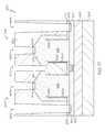
- FIG. 1is a cross-sectional view of an initial finFET semiconductor structure comprising disposable gates according to one embodiment of the present invention
- FIG. 2is a cross-sectional view of the finFET semiconductor structure after a spacer has been formed over the structure according to one embodiment of the present invention
- FIG. 3is a cross-sectional view of the finFET semiconductor structure after the spacer has been removed from the PFET region and a masking layer has been formed over the NFET region according to one embodiment of the present invention
- FIG. 4is a cross-sectional view of the finFET semiconductor structure after source and drain regions have been epitaxially grown in the PFET region according to one embodiment of the present invention
- FIG. 5is a cross-sectional view of the finFET semiconductor structure after a contact metal layer has been formed over the entire structure according to one embodiment of the present invention
- FIG. 6is a cross-sectional view of the finFET semiconductor structure after silicide/germanide has been formed on the source and drain regions of the PFET region according to one embodiment of the present invention
- FIG. 7is a cross-sectional view of the finFET semiconductor structure after a spacer and masking layer have been formed on the PFET region according to one embodiment of the present invention.
- FIG. 8is a cross-sectional view of the finFET semiconductor structure after source and drain regions have been epitaxially grown in the NFET region according to one embodiment of the present invention
- FIG. 9is a cross-sectional view of the finFET semiconductor structure after a contact metal layer has been formed over the entire structure according to one embodiment of the present invention.
- FIG. 10is a cross-sectional view of the finFET semiconductor structure after silicide/germanide has been formed on the source and drain regions of the NFET region according to one embodiment of the present invention
- FIG. 11is a cross-sectional view of the finFET semiconductor structure after an implantation process has been performed to segregate and activate dopants at the source/drain-silicide/germanide interfaces according to one embodiment of the present invention
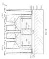
- FIG. 12is a cross-sectional view of an initial vertical FET semiconductor structure after each top source/drain has been formed in the NFET and PFET regions according to one embodiment of the present invention
- FIG. 13is a cross-sectional view of the vertical FET semiconductor structure after a dielectric layer has been formed over the structure according to one embodiment of the present invention
- FIG. 14is a cross-sectional view of the vertical FET semiconductor structure after contact trenches have been formed to expose a portion of the top source/drain and bottom source/drain in the NFET region according to one embodiment of the present invention
- FIG. 15is a cross-sectional view of the vertical FET semiconductor structure after silicide/germanide has been formed in contact with the exposed portions of the top source/drain and bottom source/drain in the NFET region according to one embodiment of the present invention
- FIG. 16is a cross-sectional view of the vertical FET semiconductor structure after contact trenches have been formed to expose a portion of the top source/drain and bottom source/drain in the PFET region and silicide/germanide has been formed in contact with the exposed portions of the top source/drain and bottom source/drain in the PFET region according to one embodiment of the present invention;
- FIG. 17is a cross-sectional view of the vertical FET semiconductor structure after a contact trench has been formed over the gate according to one embodiment of the present invention.
- FIG. 18is a cross-sectional view of the vertical FET semiconductor structure after a contact liner has been formed on the sidewalls of each contact trench and in contact with the silicides/germanides according to one embodiment of the present invention
- FIG. 19is a cross-sectional view of the vertical FET semiconductor structure after a metal contact has been formed within each of the contact trenches according to one embodiment of the present invention.
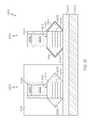
- FIG. 20is a cross-sectional view of an initial nano-sheet semiconductor structure after metal gates have been formed in the NFET and PFET regions according to one embodiment of the present invention
- FIG. 21is a cross-sectional view of the nano-sheet semiconductor structure after the NFET region has been masked off and a contact metal layer has been formed on the epitaxially grown source/drain regions in the PFET region according to one embodiment of the present invention
- FIG. 22is a cross-sectional view of the nano-sheet semiconductor structure after silicide/germanide has been formed in contact and surrounding the epitaxially grown source/drain regions in the PFET region according to one embodiment of the present invention
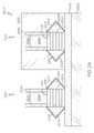
- FIG. 23is a cross-sectional view of the nano-sheet semiconductor structure after the PFET region has been masked off and a contact metal layer has been formed on the epitaxially grown source/drain regions in the NFET region according to one embodiment of the present invention
- FIG. 24is a cross-sectional view of the nano-sheet semiconductor structure after silicide/germanide has been formed in contact and surrounding the epitaxially grown source/drain regions in the NFET region according to one embodiment of the present invention
- FIG. 25is a cross-sectional view of the nano-sheet semiconductor structure after a contact liner has been formed in contact with at least the spacers and the silicide/germanide in each of the NFET and PFET regions according to one embodiment of the present invention
- FIG. 26is an operational flow diagram illustrating one process for fabricating finFET semiconductor structures according to one embodiment of the present invention.
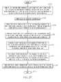
- FIG. 27is an operational flow diagram illustrating one process for fabricating vertical FET semiconductor structures according to one embodiment of the present invention.
- FIG. 28is an operational flow diagram illustrating one process for fabricating nano-sheet semiconductor structures according to one embodiment of the present invention.
- One or more embodimentsinclude a design for an integrated circuit chip, which is created in a graphical computer programming language, and stored in a computer storage medium (such as a disk, tape, physical hard drive, or virtual hard drive such as in a storage access network). If the designer does not fabricate chips or the photolithographic masks used to fabricate chips, the designer is able to transmit the resulting design by physical means (e.g., by providing a copy of the storage medium storing the design) or electronically (e.g., through the Internet) to such entities, directly or indirectly.
- the stored designis then converted into the appropriate format (e.g., GDSII) for the fabrication of photolithographic masks, which typically include multiple copies of the chip design in question that are to be formed on a wafer.
- the photolithographic masksare utilized to define areas of the wafer (and/or the layers thereon) to be etched or otherwise processed.
- the resulting integrated circuit chipsare distributable by the fabricator in raw wafer form (that is, as a single wafer that has multiple unpackaged chips), as a bare die, or in a packaged form.
- the chipis mounted in a single chip package (such as a plastic carrier, with leads that are affixed to a motherboard or other higher level carrier) or in a multichip package (such as a ceramic carrier that has either or both surface interconnections or buried interconnections).
- the chipis then integrated with other chips, discrete circuit elements, and/or other signal processing devices as part of either (a) an intermediate product, such as a motherboard, or (b) an end product.
- the end productcan be any product that includes integrated circuit chips, ranging from toys and other low-end applications to advanced computer products having a display, a keyboard or other input device, and a central processor.
- FIGS. 1-25illustrate various processes for fabricating semiconductor structures having low resistance source-drain contacts.
- FIG. 1shows a cross-section of a semiconductor structure 100 at a starting point for embodiments of the present invention.
- one or more embodiments of the present inventionbegin after semiconductor fins have been formed for NFET and PFET devices, and disposable gates have been formed thereon. It should be noted that embodiments of the present invention are not limited to the structures, layers, and materials discussed herein.
- the semiconductor structure 100 of FIG. 1comprises a substrate 102 ; a dielectric layer 104 (e.g., a BOX layer or oxide layer) overlying the substrate 102 ; one or more fin structures 106 in contact with the dielectric layer 104 ; device isolation regions 108 , 110 such as shallow trench isolation regions; and source/drain regions (not shown in this cross-section).
- a dielectric layer 104e.g., a BOX layer or oxide layer
- fin structures 106in contact with the dielectric layer 104
- device isolation regions 108 , 110such as shallow trench isolation regions
- source/drain regionsnot shown in this cross-section.
- the semiconductor structure 100comprises substrate 102 such as a silicon-on-insulator (SOI) substrate; a dielectric layer 104 (e.g., a BOX layer or oxide layer) overlying the substrate 102 ; one or more fin structures 106 , 108 overlying the dielectric layer 104 , and one or more shallow trench isolation (STI) regions 110 .
- the substrate layer 102comprises at least one of Si, Ge alloys, SiGe, GaAs, InAs, InP, SiCGe, SiC, and other III/V or II/VI compound semiconductors.
- the dielectric layer 104in one embodiment, is a crystalline or non-crystalline oxide, nitride, oxynitride, or any other insulating material.
- At least one fin 106is formed in an NFET region 112 of the structure 100 and at least one fin 108 is formed in a PFET region 114 of the structure.
- the fin(s) 106 within the NFET region 112comprise, for example, a semiconductor material such as silicon (Si), while the fin(s) 108 within the PFET region 114 comprise a semiconductor material such as silicon germanium (SiGe).
- P-type transistorsare produced by doping the semiconductor layer from which the fin 106 is formed with elements from group III of the periodic table (e.g., boron, aluminum, gallium, or indium).
- the dopantcan be boron in a concentration ranging from 1 ⁇ 10E18 atoms/cm3 to 2 ⁇ 10E21 atoms/cm3.
- N-type transistorsare produced by doping the semiconductor layer from which the fin 108 is formed with elements from group V of the periodic table (e.g., phosphorus, antimony, or arsenic).
- the semiconductor layercan be undoped or doped with either p-type or n-type dopants through ion implantation, plasma doping, or gas phase doping.
- FIG. 1further shows that a disposable gate 116 , 118 is formed over and in contact with each of the fins 106 , 108 .
- the disposable gates 116 , 118are formed, in one embodiment, using oxide, polysilicon, amorphous silicon, nitride, or a combination thereof.
- spacers 120 , 122are formed on the sidewalls of the disposable gates 116 , 118 by one or more spacer formation techniques.
- the disposable gates 116 , 118can also be real gates formed using the “gate first” integration scheme.
- An optional hard mask(not shown) can be formed on top of the dual disposable gates 116 , 118 .
- the hard maskcan comprise a dielectric material such as a nitride, oxide, oxynitride material, and/or any other suitable dielectric layer.
- the spacer 202is an iRAD spacer.
- the spacer 202is formed by forming a layer (e.g., silicon nitride (SiN)) via an iRAD process, which creates a very conformal layer and a dense film for the spacer layer from which the spacer 202 is formed.
- a layere.g., silicon nitride (SiN)
- iRAD processe.g., silicon nitride (SiN)
- Techniques other than iRADcan be used to create the spacer 202 , such as low-pressure chemical vapor deposition (LPCVD).
- LPCVDlow-pressure chemical vapor deposition
- the spacer 202is 4 nm to 12 nm thick.
- FIG. 3shows that the spacer layer 202 is selectively removed from the PFET region 114 of the structure 100 exposing the PFET fin(s) 108 , disposable gate 118 , and gate spacer 122 .
- the NFET region 112 of the structure 100is masked from the etch using a photoresist.
- a conventional mask material 302is formed on the NFET region 112 utilizing a conventional deposition process followed by lithography and etching such that only the NFET region 112 is covered by the mask 302 while the PFET region 114 is left exposed.
- the portion of the spacer layer 202 within the PFET region 114is then removed.
- a dry etching processsuch as RIE is performed to remove the spacer 202 from the PFET region 114 while the mask 302 prevents the portion of the spacer 202 within the NFET region 114 from being removed.
- the mask layer 302is removed utilizing one or more etching processes, and source/drain regions 402 , 404 are formed within the PFET region 114 , as shown in FIG. 4 .
- the source and drain regions 402 , 404are formed by an epitaxial growth process that epitaxially grows source/drain material on the fin 108 .
- the terms “epitaxial growth”, “epitaxial deposition”, “epitaxially formed”, epitaxially grown”, and their variants and/or grown”mean the growth of a semiconductor material on a deposition surface of a semiconductor material, in which the semiconductor material being grown has the same crystalline characteristics as the semiconductor material of the deposition surface.
- an epitaxial semiconductor materialhas the same crystalline characteristics as the deposition surface on which it is formed. For example, an epitaxial semiconductor material deposited on a ⁇ 100 ⁇ crystal surface will take on a ⁇ 100 ⁇ orientation.
- epitaxial growth and/or deposition processesare selective to forming on semiconductor surface, and do not deposit material on dielectric surfaces, such as silicon dioxide or silicon nitride surfaces.
- Examples of various epitaxial growth process apparatusthat are suitable for use in one or more embodiments include, e.g., rapid thermal chemical vapor deposition (RTCVD), low-energy plasma deposition (LEPD), ultra-high vacuum chemical vapor deposition (UHVCVD), atmospheric pressure chemical vapor deposition (APCVD) and molecular beam epitaxy (MBE).
- RTCVDrapid thermal chemical vapor deposition
- LEPDlow-energy plasma deposition
- UHVCVDultra-high vacuum chemical vapor deposition
- APCVDatmospheric pressure chemical vapor deposition
- MBEmolecular beam epitaxy
- the gas source for the deposition of epitaxial semiconductor materialcan include a silicon containing gas source, a germanium containing gas source, a carbon containing gas source, or a combination thereof.
- silicon containing gas sourcesare silane, disilane, trisilane, tetrasilane, hexachlorodisilane, tetrachlorosilane, dichlorosilane, trichlorosilane, methylsilane, dimethylsilane, ethylsilane, methyldisilane, dimethyldisilane, hexamethyldisilane, and combinations thereof.
- germanium containing gas sourcesare germane, digermane, halogermane, dichlorogermane, trichlorogermane, tetrachlorogermane and combinations thereof. While an epitaxial silicon germanium alloy fin can be formed utilizing a combination of such gas sources. Carrier gases like hydrogen, nitrogen, helium and argon can be used.
- the epitaxially grown source/drain regions 402 , 404 within the PFET region 114comprise SiGe, SiGeC, or a bi-layer SiGe/SiGeC stack.
- the bi-layer stackin one embodiment, is formed by introducing carbon-containing gases such as methane into the epitaxial growth chamber to grow carbon doped SiGe or SiGeC layer.
- carbon-containing gasessuch as methane
- to concentration of carbonis less than 2 atomic percent; the concentration of Ge varies from 10% to 100%; the concentration of Si is 100%—the percentage of Ge. It should be noted that other percentages also apply.
- the source and drain regions 402 , 404in one embodiment, is formed with in-situ doping of the electrical dopants (e.g., boron, aluminum, gallium, or indium), or by deposition of an intrinsic semiconductor material and subsequent introduction of electrical dopants by ion implantation, plasma doping, gas phase doping, or out-diffusion from a disposable doped silicate glass layer.
- the electrical dopantse.g., boron, aluminum, gallium, or indium
- One or more contact metal/metallic layers 502are then formed over the entire structure 100 , as shown in FIG. 5 .
- the contact metal layer 502is formed over and in contact with the spacer layer 302 in the NFET region 112 , the isolation region 110 , the source/drain 402 , 404 of the PFET device, and the disposable gate structure 118 (including the gate spacer 122 ) of the PFET device.
- the contact metal layer(s) 502in one embodiment, is formed by chemical vapor deposition (CVD), physical vapor deposition (PVD), atomic layer deposition (ALD), or any combination thereof.
- the contact metal layer(s) 502in one embodiment, comprises titanium (Ti), tantalum (Ta), hafnium (Hf), zirconium (Zr), niobium (Nb), or alloys comprising carbon. However, other materials are applicable as well.
- the sheet resistivity of the material(s) used for the contact metal layer(s) 502is less than 50 ⁇ Ohm/cm.
- the contact metal layer 502comprises one or more high melting point (e.g., greater than 1500° C.) refractory metals such as molybdenum (Mo), ruthenium (Ru), vanadium (Va), tungsten (W), or the like.
- the thickness of the metal layer 502is 3 nm to 15 nm, although lesser or greater thicknesses apply.
- the source/drain regions 402 , 404in one embodiment, comprise carbon in addition to SiGe.
- the carboncan be deposited in the top region of the epitaxy material during epitaxy growth.
- an implantation processis performed to deposit carbon in the top region of source/drains 402 , 404 after the contact metal layer 502 is formed, but prior a subsequent anneal process.
- the implantation processin one embodiment, includes, a beam line implantation of carbon with beam energies tuned to implant carbon from the surface to 20 nm below the exposed surface.
- an interlayer(not shown) comprising carbon can be formed on and in contact with a top surface of the source/drains 402 , 404 prior to forming the contact metal layer 502 .
- a pure metal(s), metal carbide, alloy, etc. comprising carboncan be deposited by CVD, PVD, ALD, or any combination thereof to form the carbon-based interlayer.
- carbonis added through incorporation in the contact metal layer 502 .
- carboncan be added during formation of the contact metal layer utilizing, for example, an alloy target, change in CVD/ALD precursor, implantation into the contact metal layer 502 , and/or the like.
- silicide/germanide 602 , 604An anneal is then performed to form a silicide/germanide 602 , 604 , as shown in FIG. 6 .
- the silicide/germanide 602 , 604is formed on and in contact with the source/drains 402 , 404 resulting from the reaction of the contact metal layer(s) 502 with the source/drain material.
- the thickness of the silicideis 5 nm to 40 nm depending on the phase of the silicide.
- the result of the annealis silicides/germanides of Ti, Ta, Hf, Zr, or Nb.
- the silicides/germanides 602 , 604comprise carbon for enhanced agglomeration resistance.
- carbonis implanted into the silicide/germanide 602 , 604 .
- the annealcan be performed at temperature ranging from, for example, 700° C. to 1250° C.
- the spacer layer 302prevents any silicide from being formed in the NFET region 112 . Unreacted metal is then selectively removed from the structure 100 .
- a spacer layer 702is formed over the PFET region, as shown in FIG. 7 .
- This spacer layer 702is similar to the spacer layer 202 discussed above with respect to FIGS. 2 and 3 .
- the spacer layer 702is formed over the entire structure 100 and selectively removed from the NFET region 112 . This exposes the NFET fin(s) 106 , disposable gate 116 , and gate spacer 120 .
- the PFET region 114 of the structure 100is masked from the etch using a photoresist.
- a conventional mask material 704is formed on the PFET region 114 utilizing a conventional deposition process followed by lithography and etching such that only the PFET region 114 is covered by the mask 302 while the NFET region 112 is left exposed. The portion of the spacer layer 704 within the NFET region 112 is then removed.
- the mask layer 704is removed utilizing one or more etching processes, and source/drain regions 802 , 804 are formed within the NFET region 112 , as shown in FIG. 8 .
- the source and drain regions 802 , 804are formed by an epitaxial growth process similar to that discussed above with respect to the PFET region 114 .
- the epitaxially grown source/drain regions 802 , 804 within the NFET region 114comprise Si:P SiC:P, SiAs, SiC:As and/or the like.
- the source and drain regions 802 , 804in one embodiment, is formed with in-situ doping of the electrical dopants (e.g., phosphorus, antimony, or arsenic), or by deposition of an intrinsic semiconductor material and subsequent introduction of electrical dopants by ion implantation, plasma doping, gas phase doping, or out-diffusion from a disposable doped silicate glass layer.
- the doping concentrationis in the range of 1E19/cm 3 to 3E21/cm 3 .
- One or more contact metal/metallic layers 902are then formed over the entire structure 100 , as shown in FIG. 9 .
- the contact metal layer 902is formed over and in contact with the source/drain 802 , 804 of the NFET device, the disposable gate structure 116 (including the gate spacer 120 ) of the NFET device, the isolation region 110 , and the spacer layer 702 in the PFET region 114 .
- the contact metal layer(s) 902in one embodiment, is formed by chemical vapor deposition (CVD), physical vapor deposition (PVD), atomic layer deposition (ALD), or any combination thereof.
- the contact metal layer(s) 902in one embodiment, comprises titanium (Ti), tantalum (Ta), TiN, hafnium (Hf), zirconium (Zr), niobium (Nb), or alloys comprising carbon. However, other materials are applicable as well.
- the sheet resistivity of the material(s) used for the contact metal layer(s) 902is less than 50 ⁇ Ohm/cm.
- the contact metal layer 902comprises one or more high melting point (e.g., greater than 1500° C.) refractory metals such as molybdenum (Mo), ruthenium (Ru), vanadium (Va), tungsten (W), or the like.
- the thickness of the metal layer 902is 3 nm to 15 nm, although lesser or greater thicknesses apply.
- the source/drain regions 802 , 804in one embodiment, comprise carbon in addition to Si:P or Si:As.
- the carboncan be deposited in the top region of the epitaxy material during epitaxy growth.
- an implantation processis performed to deposit carbon in the top region of source/drains 802 , 804 after the contact metal layer 902 is formed, but prior a subsequent anneal process, as discussed above.
- an interlayer(not shown) comprising carbon can be formed on and in contact with a top surface of the source/drains 802 , 804 prior to forming the contact metal layer 902 .
- carboncan be deposited by CVD, PVD, ALD, or any combination thereof to form the carbon-based interlayer.
- carbonis added through incorporation in the contact metal layer 902 .
- carboncan be added during formation of the contact metal layer utilizing, for example, an alloy target, change in CVD/ALD precursor, implantation into the contact metal layer 902 , and/or the like.
- silicide 1002 , 1004An anneal is then performed to form a silicide 1002 , 1004 , as shown in FIG. 10 .
- the silicide 1002 , 1004is formed on and in contact with the source/drains 802 , 804 resulting from the reaction of the contact metal layer(s) 902 with the source/drain material.
- the thickness of the silicideis 5 nm to 40 nm depending on the phase of the silicide.
- the result of the annealis silicides of Ti, Ta, Hf, Zr, or Nb.
- the silicide 1002 , 1004comprise carbon for enhanced agglomeration resistance.
- carbonis implanted into the silicide 1002 , 1004 .
- the annealcan be performed at temperature ranging from, for example, 700° C. to 1250° C. Unreacted metal is then selectively removed from the structure 100 .
- an optional implantation processcan be performed through the silicide (or germanide) 602 , 604 , 1002 , 1004 in both regions.
- the NFET regionis blocked by forming a mask layer thereon using lithography and patterning techniques.
- An implantation processis then performed to implant elements from group III of the periodic table (e.g., boron, aluminum, gallium, or indium) into the PFET silicide 602 , 604 .
- the implantation processcan include beam line or plasma implantation, and the doping concentrations are in the range of 1E20/cm3 to 5E22/cm3.
- An annealis then performed to segregate and activate the dopants at the source/drain and silicide interfaces 1102 , 1104 , as shown in FIG. 11 .
- the annealcan be performed at temperature ranging from, for example, 700° C. to 1250° C.
- the NFET region 112is protected from this implantation process by the mask.
- the maskis removed from the NFET region 112 via an ashing process.
- a maskis then formed over the PFET region 114 (similar to the NFET region 112 ) and an implantation process is performed to implant elements from group V of the periodic table (e.g., phosphorus, antimony, or arsenic) into the NFET silicide 1002 , 1004 .
- the doping concentrationis in the range of 1E19/cm 3 to 3E21/cm 3 .
- the PFET region 114is protected from this implantation process by the mask.
- an annealis then performed to segregate and activate the dopants at the source/drain and silicide interfaces 1106 , 1108 , as shown in FIG. 11 .
- the annealcan be performed at temperature ranging from, for example, 700° C. to 1250° C., although lesser and greater temperatures are applicable as well.
- the maskis removed from the PFET region 114 via an ashing process. In one embodiment, a single anneal can be performed for both the NFET region 112 and the PFET region 114 .
- Conventional fabrication techniquescan then be performed to complete the fabrication of the NFET and PFET devices. Using the above process, source-drain contacts can be fabricated with extremely low contact resistivity that are resistant to degradation via agglomeration due to downstream processing. Thus, highly reliable and low resistivity source-drain contacts can be formed.
- FIG. 12shows a vertical finFET structure 1200 at a starting point for embodiments of the present invention.
- One or more embodiments of the present inventionbegin after the top source/drain regions have been formed for the NFET and PFET devices.
- embodiments of the present inventionare not limited to the particular vertical finFET structure shown in FIG. 12 .
- Embodiments of the present inventionare applicable to any vertical finFET structure and methods for fabricating the same.
- the structure 1200comprises an NFET region 1202 and a PFET region 1204 . Both of these regions are formed on a substrate 1206 and an insulator layer 1208 .
- the NFET and PFET regions 1202 , 1204are isolated by an isolation layer 1210 .
- the thickness of the substrate 102can be, for example, from 50 microns to 1,000 microns, although lesser and greater thicknesses can be employed as well.
- the substrate 1206can be single crystalline and or a bulk substrate, a semiconductor-on-insulator (SOI) substrate, or a hybrid substrate.
- the insulator layer 1208comprises a dielectric material such as silicon oxide, silicon nitride, silicon oxynitride, or any combination thereof.
- the insulator layer 1208is a buried oxide (BOX) layer.
- An optional counter-doped layer(not shown) can be formed on and in contact with the substrate 1206 (or buried insulator layer if formed).
- the counter-doped layerin one embodiment, is formed by an epitaxial growth of a semiconductor material.
- Each region 1202 , 1204comprises a first doped layer 1212 , 1214 (also referred to herein as the “bottom source/drain layer” 1212 , 1214 ), and a channel layer 108 .
- the substrate 102can be single crystalline and or a bulk substrate, a semiconductor-on-insulator (SOI) substrate, or a hybrid substrate.
- the insulator layer 104comprises a dielectric material such as silicon oxide, silicon nitride, silicon oxynitride, or any combination thereof. In one embodiment, the insulator layer 104 is a buried oxide (BOX) layer.
- the bottom source/drain layers 1212 , 1214are formed on and in contact with the insulator layer 1208 (or counter-doped layer if formed).
- the bottom source/drain layer 1212is an n++ doped region of the substrate 1206 .
- the bottom source/drain layer 1214is a p++ doped region of the substrate 1206 .
- the bottom source/drain layers 1212 , 1214have a thickness in a range of, for example, about 10 nm to about 200 nm. However, other thicknesses are applicable as well.
- the bottom source/drain layers 1212 , 1214can be formed by epitaxial growth.
- Each of the NFET and PFET regions 1202 , 1204comprise one or more fin structures 1216 , 1218 .
- the fins 1216 , 1218are formed, for example, from a channel material that was epitaxially grown up from the bottom source/drain layers 1212 , 1214 .
- the fin(s) 1216include a material that is undoped or doped n-type dopants through ion implantation, plasma doping, or gas phase doping.
- N-type transistorsare produced by doping the channel material with elements from group V of the periodic table (e.g., phosphorus, antimony, or arsenic).
- the dopantcan be phosphorus in a concentration ranging from 1 ⁇ 10E14 atoms/cm3 to 1 ⁇ 10E20 atoms/cm3.
- the fin(s) 1218include a material that is undoped or doped n-type dopants through ion implantation, plasma doping, or gas phase doping.
- P-type transistorsare produced by doping the channel material with elements from group III of the periodic table (e.g., boron, aluminum, gallium, or indium).
- the dopantcan be boron in a concentration ranging from 1 ⁇ 10E18 atoms/cm3 to 2 ⁇ 10E21 atoms/cm3.
- FIG. 12further shows that bottom spacers 1220 , 1222 are formed within each of the NFET and PFET regions 1202 , 1204 .
- the bottom spacers 1220 , 1222are formed in contact with each of the fins 1216 , 1218 .
- Each bottom spacer 1220 , 1222contacts a top surface of their respective source/drain layer 1212 , 1214 and sidewalls of their respective fin(s) 1216 , 1218 .
- the bottom spacers 1220 , 1222comprise an insulating material (such as silicon oxide, silicon nitride, silicon oxynitride, or a combination of these) and can be formed using any conventional deposition and etching processes such as, for example, chemical vapor deposition (CVD) and subsequent etching techniques.
- the spacers 1220 , 1222have a thickness of, for example, 3 nm to 30 nm.
- High-k dielectric layers 1224 , 1226are formed on and in contact with the sidewalls of each fin 1216 , 1218 and the top surface of the bottom spacers 1220 , 1222 .
- high-k materialsinclude but are not limited to metal oxides such as hafnium oxide, hafnium silicon oxide, hafnium silicon oxynitride, lanthanum oxide, lanthanum aluminum oxide, zirconium oxide, zirconium silicon oxide, zirconium silicon oxynitride, tantalum oxide, titanium oxide, barium strontium titanium oxide, barium titanium oxide, strontium titanium oxide, yttrium oxide, aluminum oxide, lead scandium tantalum oxide, and lead zinc niobate.
- the high-k layers 1224 , 1226may further include dopants such as lanthanum or aluminum.
- the high-k layers 1224 , 1226are part of a layer comprising a work function metal layer (not shown).
- the work function metal layersare formed after and conformal to the high-k layers 1224 , 1226 employing CVD, sputtering, or plating.
- the work function metal layerscomprise one or more metals having a function suitable to tune the work function of NFETs or PFETs.
- Exemplary first metals that can be employed in the work function metal layerinclude, but are not limited to La, Ti and Ta.
- the thickness of the work function metal layerscan be from 3 nm to 15 nm, although lesser and greater thicknesses can also be employed.
- FIG. 12further shows that a metal gate 1228 is formed around the fins 1216 , 1218 .
- a metal gate materialcan be deposited by atomic layer deposition (ALD) or physical vapor deposition (PVD).
- the metal gate 1228is a continuous metal gate that wraps around both fins 1216 , 1218 .
- the metal gate 1228contacts the outer sidewalls of the high-k gate dielectric layers 1224 , 1226 ; the top surface of a portion of the bottom spacers 1220 , 1222 ; and a top surface of the dielectric 1210 formed between the fins 1216 , 1218 .
- a top surface of the metal gate 1228is co-planar with the top surface of the high-k dielectric layers 1224 , 1226 .
- the metal gate 1228comprises, for example, tungsten.
- Each of the NFET and PFET regions 1202 , 1204also include top spacers 1230 , 1232 .
- the top spacers 1230 , 1232comprise a bottom surface that contacts the top surface of the metal gate 1228 ; the top surface of the high-k dielectric layers 1224 , 1226 ; and portions of the sidewalls of the fins 1216 , 1218 that are above the metal gate 1228 and the high-k dielectric layers 1216 , 1218 .
- the top surface of the top spacers 1230 , 1232is co-planar with the top surfaces of the fins 1216 , 1218 .
- the top spacers 1230 , 1232comprise the same or different material as the bottom spacers 1220 , 1222 .
- the top spacers 1230 , 1232can comprise an insulating material (such as silicon oxide, silicon nitride, silicon oxynitride, or a combination of these) and can be formed using any conventional deposition process such as, for example, chemical vapor deposition (CVD) and subsequent etching techniques. The deposited spacer material is then subsequently etched to form the final spacer structures.
- an insulating materialsuch as silicon oxide, silicon nitride, silicon oxynitride, or a combination of these
- CVDchemical vapor deposition
- FIG. 12further shows a doped layer 1234 , 1236 (also referred to herein as the “top source/drain layer”) formed on and in contact with each the fins 1216 , 1218 and their respective top spacer 1230 , 1232 .
- a bottom surface of the top source/drain layers 1234 , 1236contacts a top surface of the fins 1216 , 1218 and a top surface of the top spacers 1230 , 1232 .
- the top source/drain layers 1234 , 1236have a thickness in a range of, for example, about 10 nm to about 200 nm. However, other thicknesses are applicable as well.
- the top source/drain layers 1234 , 1236can be formed by epitaxial growth.
- the top source/drain layers 1234 , 1236have a “diamond-shaped/cross-section”. It should be noted that, in other embodiments, the top source/drain layers 1234 , 1236 do not include a diamond-shaped/cross-section and has a planar configuration. In these embodiments, the top source/drain 1204 is formed on and in contact with each the fins 106 , 108 , 110 and the top spacer layer 1108 . A bottom surface of the top source/drain layer 1204 contacts the top surface of the fins 106 , 108 , 110 and the top surface of the top spacer 1108 .
- the top source/drain layer 1204has a thickness in a range of, for example, about 10 nm to about 200 nm. However, other thicknesses are applicable as well. In any of the embodiment, the top source/drain layer 1204 can be formed by epitaxial growth.
- a dielectric layer 1302is formed over the entire structure 1200 , as shown in FIG. 13 . It should be noted that a portion of this dielectric can be formed during the fabrication of the structure 1200 shown in FIG. 12 . In this embodiment, an additional dielectric layer can be formed on top of the previous layer to form the dielectric layer shown in FIG. 13 .
- the dielectric layer 1302includes SiO2, Si3N4, SiOxNy, SiC, SiCO, SiCOH, and SiCH compounds; one or more silicon-based materials with some or all of the Si replaced by Ge; carbon-doped oxides; inorganic oxides; inorganic polymers; hybrid polymers; organic polymers such as polyamides or SiLKTM; other carbon-base materials; organo-inorganic materials such as spin-on glasses and silsesquioxane-based materials; and diamond-like carbon (DLC, also known as amorphous hydrogenated carbon, ⁇ -C:H). Additional choices for the blanket dielectric include any of the aforementioned materials in porous form, or in a form that changes during processing to or from being porous and/or permeable to being non-porous and/or non-permeable.
- the dielectric layer 1302is then patterned and etched to form a first contact opening/trench 1402 down to and exposing at least a portion of the bottom source/drain 1212 in the NFET region 1202 (or PFET region 1204 ), as shown in FIG. 14 .
- the dielectric layeris also patterned and etched to form a second contact opening 1404 down to and exposing a portion of the top source/drain 1234 in the NFET region 1202 .
- a mask(not shown) is formed over the PFET region 1204 to prevent any etching of the dielectric 1302 in the PFET region 1204 .
- the contact metal layer(s) 902in one embodiment, is formed by chemical vapor deposition (CVD), physical vapor deposition (PVD), atomic layer deposition (ALD), or any combination thereof.
- the contact metal layer(s) 902in one embodiment, comprises titanium (Ti), tantalum (Ta), TiN, hafnium (Hf), zirconium (Zr), niobium (Nb), or alloys comprising carbon.
- the sheet resistivity of the material(s) used for the contact metal layer(s) 902is less than 50 ⁇ Ohm/cm.
- the contact metal layer 1403comprises one or more high melting point (e.g., greater than 1500° C.) refractory metals such as molybdenum (Mo), ruthenium (Ru), vanadium (Va), tungsten (W), or the like.
- the thickness of the metal layer 1403is 3 nm to 15 nm, although lesser or greater thicknesses apply.
- an interlayer(not shown) comprising carbon can be formed on and in contact with the exposed portions of the bottom source/drain 1212 and the exposed portions of the top source/drain 1234 prior to forming the contact metal layer 1403 .
- a pure metal(s), metal carbide, alloy, etc. comprising carboncan be deposited by CVD, PVD, ALD, or any combination thereof to form the carbon-based interlayer.
- carbonis added through incorporation in the contact metal layer 1403 .
- carboncan be added during formation of the contact metal layer utilizing, for example, an alloy target, change in CVD/ALD precursor, implantation into the contact metal layer 1403 , and/or the like.
- silicide 1502 , 1504An anneal is then performed to form a silicide 1502 , 1504 , as shown in FIG. 15 .
- the silicide 1502 , 1504is formed on and in contact with the exposed portions of the bottom and top source/drain 1212 , 1234 within the first and second contact openings 1402 , 1404 , respectively, resulting from the reaction of the contact metal layer(s) 1403 with the source/drain material.
- the thickness of the silicideis 5 nm to 40 nm depending on the phase of the silicide.
- the result of the annealis silicides or germanides 1502 , 1504 of Ti, Ta, Hf, Zr, or Nb.
- the silicides/germanides 1502 , 1504comprise carbon for enhanced agglomeration resistance. In one embodiment, carbon is implanted into the silicide/germanide 1502 , 1504 . Unreacted metal is then selectively removed from the structure 1200 .
- a similar processis performed in the PFET region 1204 to form third and fourth contact openings 1602 , 1604 exposing portions of the bottom source/drain 1214 and top source/drains 1236 , respectively, as shown in FIG. 16 .
- the NFET region 1202is masked off by filling the first and second contact openings 1402 , 1404 and the remaining surfaces of the NFET region 1202 with masking material.
- One or more contact metal/metallic layersare then formed over the entire structure and an etch is performed to remove contact metal layer from all surfaces except the exposed portions of the bottom source/drain 1214 within the third contact opening 1602 and the exposed portions of the top source/drain 1236 within the fourth contact opening 1604 .
- the contact metal layer(s) 902in one embodiment, comprises titanium (Ti), tantalum (Ta), TiN, hafnium (Hf), zirconium (Zr), niobium (Nb), or alloys comprising carbon. However, other materials are applicable as well.
- the sheet resistivity of the material(s) used for the contact metal layer(s) 902is less than 50 ⁇ Ohm/cm.
- the contact metal layer 902comprises one or more high melting point refractory metals such as molybdenum (Mo), ruthenium (Ru), vanadium (Va), tungsten (W), or the like. Carbon, in one embodiment, is formed/deposited similar to that already discussed above.
- silicide 1606 , 1608An anneal is then performed to form a silicide 1606 , 1608 .
- the silicide 1606 , 1608is formed on and in contact with the exposed portions of the bottom and top source/drain 1214 , 1236 within the third and fourth contact openings 1602 , 1604 , respectively, resulting from the reaction of the contact metal layer(s) with the source/drain material.
- the result of the annealis silicides of Ti, Ta, Hf, Zr, or Nb.
- the silicide 1606 , 1608in one embodiment, comprises carbon similar to that already discussed above. Unreacted metal is then selectively removed from the structure 1200 .
- the first, second, third, and fourth contact openingscan be formed during the same process and a single anneal can be performed to form the silicides 1502 , 1504 , 1606 , 1608 .
- an optional implantation processcan be performed through the silicide (or germanide) 1502 , 1504 , 1606 , 1608 in both regions.
- FIG. 17shows that after the contact silicides 1502 , 1504 , 1606 , 1608 have been formed, any exposed contact openings 1602 , 1604 are masked and a fifth trench 1702 is formed in the dielectric layer 1302 using lithography, patterning, and etching techniques.
- the fifth trench 1702exposes a portion of the top spacer 1230 between the NFET and PFET regions 1202 , 1204 that is in contact with the gate 1228 .
- any masking materialis removed from the structure 1200 using one or more etching processes.
- contact metalor conductive contact
- contact openings 1402 , 1404 , 1602 , 1604 , 1702are lined with one or more contact liners 1802 , 1804 , 1806 , 1808 , 1810 .
- contact linersrefers generally to any film or layer which forms part of the resultant contact structure, and includes one or more conformally-deposited high resistive contact liners, such as a gettering layer, and a barrier/adhesive layer disposed over gettering layer.
- Gettering layercan be deposited, to ensure that oxygen (for instance, formed due to exposure of the underlying silicide to ambient conditions), remaining after various post pre-clean conditions such as, for example, argon (Ar) sputter, SiCoNi dry etch conditions, is gettered of the underlying silicide layer and also to decrease subsequent contact resistance.
- various post pre-clean conditionssuch as, for example, argon (Ar) sputter, SiCoNi dry etch conditions
- Gettering layerwhich can be deposited using conventional process(es) such as, for example, ionized metal plasma (IMP), or physical vapor deposition processes, for example, radio-frequency physical vapor deposition (RFPVD), can have a thickness of about 2 nanometers to about 8 nanometers, and be fabricated of, for example, ruthenium (Ru), an alloy of ruthenium, titanium (Ti), an alloy of titanium, tantalum (Ta), an alloy of tantalum, and the like.
- IMPionized metal plasma
- RFPVDradio-frequency physical vapor deposition
- a Barrier/adhesive layer(not shown), in one embodiment, is deposited over the gettering layer to, for instance, protect the gettering layer from eroding on exposure to harsher chemistries typically employed during subsequent contact metallization, as well as to prevent oxidation due to exposure to air.
- the Barrier/adhesive layeris deposited using conventional deposition processes, such as, for example, physical vapor deposition (PVD), chemical vapor deposition (CVD), pulsed CVD, plasma-enhanced CVD (PECVD), metal organic chemical vapor deposition (MOCVD), atomic layer deposition (ALD), plasma-enhanced ALD (PE-ALD) or sputtering methods, and has a thickness of about 1 nanometers to about 3 nanometers.
- PVDphysical vapor deposition
- CVDchemical vapor deposition
- PECVDplasma-enhanced CVD
- MOCVDmetal organic chemical vapor deposition
- ALDatomic layer deposition
- PE-ALDplasma-enhanced ALD
- sputtering methodsand has a thickness of about 1 nanometers to about 3 nanometers.
- the barrier/adhesive layerincludes, titanium-based materials (e.g., TiN, TiC, TiCN, TiSiN), or tantalum-based materials (e.g., TaN, TaC, TaCN, TaSiN) or fluorine-free tungsten-based materials (e.g., WN, WC, WCN, WSiN).
- titanium-based materialse.g., TiN, TiC, TiCN, TiSiN
- tantalum-based materialse.g., TaN, TaC, TaCN, TaSiN
- fluorine-free tungsten-based materialse.g., WN, WC, WCN, WSiN.
- titanium nitrideis formed using a titanium precursor, such as, for example, tetrakis(dimethylamino) titanium (TDMAT) or titanium tetrachloride (TiCl.sub.4) and a reagent plasma, such as, for example, nitrogen plasma during a plasma-enhanced ALD (PE-ALD) process.
- a titanium precursorsuch as, for example, tetrakis(dimethylamino) titanium (TDMAT) or titanium tetrachloride (TiCl.sub.4)
- a reagent plasmasuch as, for example, nitrogen plasma during a plasma-enhanced ALD (PE-ALD) process.
- Contact structures 1902 , 1904 , 1906 , 1908 , 1910are then formed in the contact openings 1402 , 1404 , 1602 , 1604 , 1702 , as shown in FIG. 19 .
- the contact structuresare formed by providing a conductive contact material over the contact liners (if formed) within the contact openings.
- the conductive materialin one embodiment, includes (but is not limited to) tungsten, copper, aluminum, silver, gold, and alloys thereof.
- a nucleation layer(not shown) can be deposited over the liners 1802 to 1810 to facilitate the subsequent formation of the bulk tungsten material, using conventional deposition processes such as chemical vapor deposition (CVD), atomic layer deposition (ALD) or pulsed nucleation layer deposition (PNL) deposition processes.
- CVDchemical vapor deposition
- ALDatomic layer deposition
- PNLpulsed nucleation layer deposition
- the thickness of the nucleation layerin one embodiment, is deposited by, for instance, performing alternating pulsing sequences of boron-containing reducing agent and tungsten-containing precursor in presence of a reducing agent.
- the boron-containing reducing agentsinclude, but are not limited to borane, diborane, triborane, boron halides such as, for example, boron trifluoride, boron, and the like.
- the tungsten-containing precursorscan include tungsten-containing gases such as, for example, WF 6 , WCl 6 and W(CO) 6 , and the like, while the reducing agents can include hydrogen gas, silane, disilane, hydrazine, and germane.
- the bulk deposition processinvolves a chemical vapor deposition (CVD) reaction of tungsten-containing precursor, such as tungsten hexafluoride, and reducing gases, such as hydrogen to produce tungsten and a by-product, such as for example, hydrogen hexafluoride (HF) at temperature of about 250° C. to about 400° C. Any excess contact liners material and excess conductive contact material are polished away.
- CVDchemical vapor deposition
- FIG. 20shows another example of a semiconductor structure 2000 applicable to embodiments of the present invention.
- FIG. 20shows one example of a nano-sheet semiconductor structure 2000 at a starting point for embodiments of the present invention.
- one or more embodimentsbegin after source/drain regions have been epitaxially formed.
- embodiments of the present inventionare not limited to the particular nano-sheet device structure shown in FIG. 20 .
- Embodiments of the present inventionare applicable to nano-sheet device structure and methods for fabricating the same.
- the structure 200comprises an NFET region 2002 and a PFET region 2004 . Both of these regions are formed on a substrate 2006 and an insulator layer 2008 .
- the handle substrate 2006includes a semiconductor material, an insulator material, a conductive material, or a combination thereof.
- the thickness of the handle substrate 2006in one embodiment, ranges from 50 microns to 2 mm, although lesser and greater thicknesses can also be employed.
- the insulator layer 2008includes a dielectric material such as silicon oxide, silicon nitride, silicon oxynitride, or a combination thereof.
- the insulator layer 2008in one embodiment, has a thickness ranging from 5 nm to 500 nm, although lesser and greater thicknesses can also be employed.
- the structure 2000 of FIG. 20also comprises a first stack 2010 formed in the NFET region 2002 and a second stack 2012 formed in the PFET region 2004 .
- Each of these stacks 2010 , 2012comprises alternating layers of a semiconductor material 2014 , 2016 (e.g., nano-sheets) and a gate material 2018 , 2020 .
- the alternating layers of the semiconductor material 2014 , 2016include a silicon-containing semiconductor material.
- silicon-containing semiconductor materialsinclude pure, i.e., unalloyed, silicon, carbon doped silicon (Si:C), or a silicon germanium alloy having a germanium content of “significantly” less germanium (i.e., 30% or more germanium content difference). However, other materials and concentrations are applicable as well.
- the alternating layers of the gate material 2018 , 2020comprise a conductive material used to form at least the gate conductor portion of a gate 2022 , 2024 formed on an in contact with each of the stacks 2010 , 2014 .
- the gate material 2018 , 2020comprises any conductive material including, for example, doped polysilicon, an elemental metal (e.g., tungsten, titanium, tantalum, aluminum, nickel, ruthenium, palladium and platinum), an alloy of at least two elemental metals, an elemental metal nitride (e.g., tungsten nitride, aluminum nitride, and titanium nitride), an elemental metal silicide (e.g., tungsten silicide, nickel silicide, and titanium silicide) or multilayered combinations thereof.
- the conductive materialcan also be an NFET or a PFET gate metal.
- the structure 2000further comprises source regions 2026 , 2028 and drain regions 2030 , 2032 that have been epitaxially grown on and in contact with the first and second stacks 2010 , 2012 .
- the source regions 2026 , 2028 and drain regions 2030 , 2032have a “diamond-shaped/cross-section” resulting from the epitaxy growth process. It should be noted that, in other embodiments, the source regions 2026 , 2028 and drain regions 2030 , 2032 do not include a diamond-shaped/cross-section and has a planar configuration.
- the gate structures 2022 , 2024are formed on and in contact with their respective stack 2010 , 2012 , and are comprised of the gate material 2018 , 2020 discussed above.
- the gate structures 2022 , 2024wrap around the semiconductor layers 2014 , 2016 of the stacks 2010 , 2012 .
- the gate structures 2022 , 2024also comprise a dielectric material (not shown).
- the dielectric materialcomprises, for example, oxide, nitride, and/or oxynitride.
- the gate dielectric materialis a high-k material having a dielectric constant greater than silicon dioxide.
- high-k dielectricsinclude, but are not limited to, HfO 2 , ZrO 2 , La 2 O 3 , Al 2 O 3 , TiO 2 , SrTiO 3 , LaAlO 3 , Y 2 O 3 , HfO x N y , ZrO x N y , La 2 O x N y , Al 2 O x N y , TiO x N y , SrTiO x N y , LaAlO x N y , Y 2 O x N y , SiON, SiN x , a silicate thereof, and an alloy thereof.
- FIG. 20shows a replacement gate structure 2022 , 2024 , embodiments of the present invention can be performed prior to removal of the disposable gate.
- FIG. 20further shows that a cap layer 2034 , 2036 is formed on and in contact with a top surface of the gate structures 2022 , 2024 .
- the cap layers 2034 , 2036in one embodiment, comprise a dielectric material such as silicon nitride, silicon oxide, or a dielectric metal oxide.
- Gate spacers 2038 , 2040are formed around (wrapping) each of the gate structures 2022 , 2024 .
- the gate spacers 2038 , 2040in one embodiment comprise a dielectric material layer.
- the NFET region 2002is masked off. For example, a masking material is deposited followed by lithography and etching such that only the NFET region 2002 is covered by a mask 2102 while the PFET region 2004 is left exposed, as shown in FIG. 21 .
- One or more contact metal/metallic layersare then formed over the entire structure and. An etch is performed resulting in contact metal layers 2014 , 2016 remaining only on the source region 2028 and the drain region 2032 of the PFET device.
- the contact metal layer(s) 2104 , 2106in one embodiment, is formed by chemical vapor deposition (CVD), physical vapor deposition (PVD), atomic layer deposition (ALD), or any combination thereof.
- the contact metal layer(s) 902in one embodiment, comprises titanium (Ti), tantalum (Ta), TiN, hafnium (Hf), zirconium (Zr), niobium (Nb), or alloys comprising carbon.
- the sheet resistivity of the material(s) used for the contact metal layer(s) 2014 , 2016is less than 50 ⁇ Ohm/cm.
- the contact metal layer 2014 , 2016comprises one or more high melting point (e.g., greater than 1500° C.) refractory metals such as molybdenum (Mo), ruthenium (Ru), vanadium (Va), tungsten (W), or the like.
- the thickness of the contact metal layer(s) 2014 , 2016is 3 nm to 15 nm, although lesser or greater thicknesses apply.
- an interlayer(not shown) comprising carbon can be formed on and in contact with a top surface of the source region 2028 and the drain region 2032 prior to forming the contact metal layer 2014 , 2016 .
- a pure metal(s), metal carbide, alloy, etc. comprising carboncan be deposited by CVD, PVD, ALD, or any combination thereof to form the carbon-based interlayer.
- carbonis added through incorporation in the contact metal layer 2104 , 2106 .
- carboncan be added during formation of the contact metal layer utilizing, for example, an alloy target, change in CVD/ALD precursor, implantation into the contact metal layer 2104 , 2106 , and/or the like.
- silicide 2202 , 2204An anneal is then performed to form a silicide 2202 , 2204 , as shown in FIG. 22 .
- the silicide 2202 , 2204is formed in contact with and wraps around the source region 2028 and the drain region 2032 , resulting from the reaction of the contact metal layer(s) with the source/drain material.
- the thickness of the silicideis 5 nm to 40 nm depending on the phase of the silicide.
- the result of the annealis silicides or germanides 2202 , 2204 of Ti, Ta, Hf, Zr, or Nb.
- the silicides/germanides 2202 , 2204comprise carbon for enhanced agglomeration resistance.
- carbonis implanted into the silicide/germanide 2202 , 2204 . Unreacted metal is then selectively removed from the structure 2000 .
- a similar processis then performed to form silicides/germanides in the NFET region 2002 .
- the PFET region 2004is masked off.
- a masking materialis deposited followed by lithography and etching such that only the PFET region 2004 is covered by a mask 2302 while the NFET region 2002 is left exposed, as shown in FIG. 23 .
- One or more contact metal/metallic layersare then formed over the entire structure and. An etch is performed resulting in contact metal layers 2304 , 2306 remaining only on the source region 2026 and the drain region 2030 of the NFET device.
- the contact metal layer(s) 2304 , 2306in one embodiment, is formed by chemical vapor deposition (CVD), physical vapor deposition (PVD), atomic layer deposition (ALD), or any combination thereof.
- the contact metal layer(s) 2304 , 2306in one embodiment, comprises titanium (Ti), tantalum (Ta), TiN, hafnium (Hf), zirconium (Zr), niobium (Nb), or alloys comprising carbon.
- the sheet resistivity of the material(s) used for the contact metal layer(s) 2304 , 2306is less than 50 ⁇ Ohm/cm.
- the contact metal layer 2304 , 2306comprises one or more high melting point refractory metals such as molybdenum (Mo), ruthenium (Ru), vanadium (Va), tungsten (W), or the like.
- Momolybdenum
- Ruruthenium
- Vavanadium
- Wtungsten
- the thickness of the contact metal layer(s) 2304 , 2306is 3 nm to 15 nm, although lesser or greater thicknesses apply.
- an interlayer(not shown) comprising carbon can be formed on and in contact with a top surface of the source region 2026 and the drain region 2030 similar to that discussed above.
- carbonis added through incorporation in the contact metal layer 2304 , 2306 as discussed above.
- silicide 2402 , 2404An anneal is then performed to form a silicide 2402 , 2404 , as shown in FIG. 24 .
- the silicide 2402 , 2406is formed in contact with and wraps around the source region 2026 and the drain region 2030 , resulting from the reaction of the contact metal layer(s) with the source/drain material.
- the result of the annealis silicides or germanides 2402 , 2406 of Ti, Ta, Hf, Zr, or Nb.
- the silicides/germanides 2402 , 2406comprise carbon for enhanced agglomeration resistance.
- carbonis implanted into the silicide/germanide 2402 , 2404 . Unreacted metal is then selectively removed from the structure 2000 .
- an optional implantation processcan be performed through the silicide (or germanide) 2202 , 2204 , 2402 , 2404 in both regions.
- a contact liner 2502 , 2504is then formed on and in contact with the NFET and PFET devices.
- the contact liner 2502 , 2504is formed on and in contact with the source region 2026 , 2028 ; the drain region 2030 , 2032 ; and the gate spacers 2038 , 2040 of the NFET and PFET devices.
- Conventional fabrication processescan then be performed to form contacts and complete fabrication of the devices.
- FIG. 26is an operational flow diagram illustrating one process for fabricating a finFET semiconductor structure. It should be noted that each of the steps shown in FIG. 26 has been discussed in greater detail above with respect to FIGS. 1-11 .
- the operational flow diagrambegins at step 2602 and flows directly to step 2604 .
- At least one structure, at step 2604is formed on a substrate including at least one semiconductor fin, a disposable gate formed in contact with the semiconductor fin, and a spacer in contact with the disposable gate and the semiconductor fin.
- a source region and a drain regionare epitaxially grown at least partially within the semiconductor fin, at step 2606 .
- a contact metal layer, at step 2608is formed on and in contact with the source region and the drain region.
- One of a silicide and a germanide, at step 2610is formed on the source region and the drain region from the contact metal layer prior to removing the disposable gate, forming.
- the control flowthen exits at step 2612 .
- FIG. 27is an operational flow diagram illustrating one process for fabricating a vertical FET semiconductor structure. It should be noted that each of the steps shown in FIG. 27 has been discussed in greater detail above with respect to FIGS. 12-19 .
- the operational flow diagrambegins at step 2702 and flows directly to step 2704 .
- a structure, at step 2704is formed including at least a substrate, a first source/drain layer, at least one semiconductor fin disposed on and in contact with the first source/drain layer, a gate structure in contact with the at least one semiconductor fin, and a second source/drain layer disposed on the gate structure.
- a dielectric layer, at step 2706is formed over the structure.
- a first contact trenchis formed in the dielectric layer exposing a portion of the first source/drain layer, and at least a second contact trench is formed in the dielectric layer exposing at least a portion of the second source/drain layer, at step 2708 .
- a first contact metal layeris formed on and in contact with the exposed portion of the first source/drain layer, and a second contact metal layer is formed on and in contact with the exposed portion of the second source/drain layer, at step 2710 .
- One of a first silicide and a first germanideis formed in contact with the first source/drain layer from the first contact metal layer, and one of a second silicide and a second germanide is formed in contact with the second source/drain layer from the second contact metal layer, at step 2712 .
- a first contact lineris formed on and in contact with sidewalls of the first contact trench and the one of the first silicide and the first germanide, and a second contact liner is formed on and in contact with sidewalls of second contact trench and the one of the second silicide and the second germanide, at step 2714 .
- a first metal contactis formed within the first contact trench in contact with the first contact liner, and at least a second metal is formed in contact within the second contact liner, at step 2716 .
- the control flowthen exits at step 2718 where conventional fabrication techniques are performed to complete the fabrication of the vertical FET semiconductor structure.
- FIG. 28is an operational flow diagram illustrating one process for fabricating a nano-sheet semiconductor structure. It should be noted that each of the steps shown in FIG. 28 has been discussed in greater detail above with respect to FIGS. 20-25 .
- the operational flow diagrambegins at step 2802 and flows directly to step 2804 .
- a structure, at step 2804is formed including at least an alternating stack of semiconductor layers and metal gate material layers in contact with a substrate, a metal gate formed on and in contact with a top layer of the alternating stack, a spacer in contact with at least the metal gate, a source region, and a drain region in contact with the semiconductor layers of the alternating stack.
- a first contact metal layeris formed in contact with the source region, and a second contact metal layer is formed in contact with the drain region, at step 2806 .
- One of a first silicide and a first germanide siformed in contact with and surrounding the source region, and one of a second silicide and a second germanide is formed in contact with and surrounding the drain region, at step 2808 .
- a first contact lineris formed on and in contact with the first silicide and the spacer, and a second contact liner is formed on and in contact with the second silicide and the spacer, at step 2810 .
- the control flowthen exits at step 2812 where conventional fabrication techniques are performed to complete the fabrication of the nano-sheet semiconductor structure.
Landscapes
- Engineering & Computer Science (AREA)
- Physics & Mathematics (AREA)
- Microelectronics & Electronic Packaging (AREA)
- General Physics & Mathematics (AREA)
- Manufacturing & Machinery (AREA)
- Computer Hardware Design (AREA)
- Condensed Matter Physics & Semiconductors (AREA)
- Power Engineering (AREA)
- High Energy & Nuclear Physics (AREA)
- Health & Medical Sciences (AREA)
- Toxicology (AREA)
- Chemical & Material Sciences (AREA)
- Crystallography & Structural Chemistry (AREA)
- Thin Film Transistor (AREA)
- Insulated Gate Type Field-Effect Transistor (AREA)
Abstract
Description
- The present invention generally relates to the field of semiconductors, and more particularly relates to forming contact silicide on semiconductor structures.
- Silicide/source-drain interface resistance is a major contributor to the total external parasitic resistance of semiconductor devices. As the source-drain contact dimensions are aggressively scaled, new approaches/methods are needed to reduce the interface resistance.
- In one embodiment, a method for fabricating a semiconductor structure is provided. The method includes forming at least one structure on a substrate including at least one semiconductor fin, a disposable gate formed in contact with the semiconductor fin, and a spacer in contact with the disposable gate and the semiconductor fin. A source region and a drain region are epitaxially grown at least partially within the semiconductor fin. A contact metal layer is formed on and in contact with the source region and the drain region. One of a silicide and a germanide is formed on the source region and the drain region from the contact metal layer prior to removing the disposable gate, forming.
- In another embodiment, a semiconductor structure is provided. The semiconductor structure includes at least a substrate and at least one semiconductor fin disposed on the substrate. A disposable gate contacts the at least one semiconductor fin. A spacer is disposed on the at least one semiconductor fin and in contact with the disposable gate. Epitaxially grown source and drain regions are disposed at least partially within the at least one semiconductor fin. A first one of silicide and germanide is disposed on and in contact with the source region. A second one of one of silicide and germanide is disposed on and in contact with the drain region.
- In yet another embodiment, an integrated circuit is provided. The integrated circuit includes a semiconductor structure. The semiconductor structure includes at least a substrate and at least one semiconductor fin disposed on the substrate. A disposable gate contacts the at least one semiconductor fin. A spacer is disposed on the at least one semiconductor fin and in contact with the disposable gate. Epitaxially grown source and drain regions are disposed at least partially within the at least one semiconductor fin. A first one of silicide and germanide is disposed on and in contact with the source region. A second one of one of silicide and germanide is disposed on and in contact with the drain region.
- In a further embodiment, a method for forming a semiconductor structure is provided. The method includes forming at least one structure comprising at least a substrate, a first source/drain layer, at least one semiconductor fin disposed on and in contact with the first source/drain layer, a gate structure in contact with the at least one semiconductor fin, and a second source/drain layer disposed on the gate structure. A dielectric layer is formed over the structure. A first contact trench is formed in the dielectric layer exposing a portion of the first source/drain layer. At least a second contact trench is formed in the dielectric layer exposing at least a portion of the second source/drain layer. A first contact metal layer is formed on and in contact with the exposed portion of the first source/drain layer. A second contact metal layer is formed on and in contact with the exposed portion of the second source/drain layer. One of a first silicide and a first germanide is formed in contact with the first source/drain layer from the first contact metal layer. One of a second silicide and a second germanide is formed in contact with the second source/drain layer from the second contact metal layer.
- In another embodiment, a method for forming a semiconductor structure is provided. The method includes forming at least one structure comprising at least an alternating stack of semiconductor layers and metal gate material layers in contact with a substrate, a metal gate formed on and in contact with a top layer of the alternating stack, a spacer in contact with at least the metal gate, a source region, and a drain region in contact with the semiconductor layers of the alternating stack. A first contact metal layer is formed in contact with the source region. A second contact metal layer is formed in contact with the drain region. One of a first silicide and a first germanide is formed in contact with and surrounding the source region. One of a second silicide and a second germanide is formed in contact with and surrounding the drain region.
- The accompanying figures where like reference numerals refer to identical or functionally similar elements throughout the separate views, and which together with the detailed description below are incorporated in and form part of the specification, serve to further illustrate various embodiments and to explain various principles and advantages all in accordance with the present invention, in which:
FIG. 1 is a cross-sectional view of an initial finFET semiconductor structure comprising disposable gates according to one embodiment of the present invention;FIG. 2 is a cross-sectional view of the finFET semiconductor structure after a spacer has been formed over the structure according to one embodiment of the present invention;FIG. 3 is a cross-sectional view of the finFET semiconductor structure after the spacer has been removed from the PFET region and a masking layer has been formed over the NFET region according to one embodiment of the present invention;FIG. 4 is a cross-sectional view of the finFET semiconductor structure after source and drain regions have been epitaxially grown in the PFET region according to one embodiment of the present invention;FIG. 5 is a cross-sectional view of the finFET semiconductor structure after a contact metal layer has been formed over the entire structure according to one embodiment of the present invention;FIG. 6 is a cross-sectional view of the finFET semiconductor structure after silicide/germanide has been formed on the source and drain regions of the PFET region according to one embodiment of the present invention;FIG. 7 is a cross-sectional view of the finFET semiconductor structure after a spacer and masking layer have been formed on the PFET region according to one embodiment of the present invention;FIG. 8 is a cross-sectional view of the finFET semiconductor structure after source and drain regions have been epitaxially grown in the NFET region according to one embodiment of the present invention;FIG. 9 is a cross-sectional view of the finFET semiconductor structure after a contact metal layer has been formed over the entire structure according to one embodiment of the present invention;FIG. 10 is a cross-sectional view of the finFET semiconductor structure after silicide/germanide has been formed on the source and drain regions of the NFET region according to one embodiment of the present invention;FIG. 11 is a cross-sectional view of the finFET semiconductor structure after an implantation process has been performed to segregate and activate dopants at the source/drain-silicide/germanide interfaces according to one embodiment of the present invention;FIG. 12 is a cross-sectional view of an initial vertical FET semiconductor structure after each top source/drain has been formed in the NFET and PFET regions according to one embodiment of the present invention;FIG. 13 is a cross-sectional view of the vertical FET semiconductor structure after a dielectric layer has been formed over the structure according to one embodiment of the present invention;FIG. 14 is a cross-sectional view of the vertical FET semiconductor structure after contact trenches have been formed to expose a portion of the top source/drain and bottom source/drain in the NFET region according to one embodiment of the present invention;FIG. 15 is a cross-sectional view of the vertical FET semiconductor structure after silicide/germanide has been formed in contact with the exposed portions of the top source/drain and bottom source/drain in the NFET region according to one embodiment of the present invention;FIG. 16 is a cross-sectional view of the vertical FET semiconductor structure after contact trenches have been formed to expose a portion of the top source/drain and bottom source/drain in the PFET region and silicide/germanide has been formed in contact with the exposed portions of the top source/drain and bottom source/drain in the PFET region according to one embodiment of the present invention;FIG. 17 is a cross-sectional view of the vertical FET semiconductor structure after a contact trench has been formed over the gate according to one embodiment of the present invention;FIG. 18 is a cross-sectional view of the vertical FET semiconductor structure after a contact liner has been formed on the sidewalls of each contact trench and in contact with the silicides/germanides according to one embodiment of the present invention;FIG. 19 is a cross-sectional view of the vertical FET semiconductor structure after a metal contact has been formed within each of the contact trenches according to one embodiment of the present invention;FIG. 20 is a cross-sectional view of an initial nano-sheet semiconductor structure after metal gates have been formed in the NFET and PFET regions according to one embodiment of the present invention;FIG. 21 is a cross-sectional view of the nano-sheet semiconductor structure after the NFET region has been masked off and a contact metal layer has been formed on the epitaxially grown source/drain regions in the PFET region according to one embodiment of the present invention;FIG. 22 is a cross-sectional view of the nano-sheet semiconductor structure after silicide/germanide has been formed in contact and surrounding the epitaxially grown source/drain regions in the PFET region according to one embodiment of the present invention;FIG. 23 is a cross-sectional view of the nano-sheet semiconductor structure after the PFET region has been masked off and a contact metal layer has been formed on the epitaxially grown source/drain regions in the NFET region according to one embodiment of the present invention;FIG. 24 is a cross-sectional view of the nano-sheet semiconductor structure after silicide/germanide has been formed in contact and surrounding the epitaxially grown source/drain regions in the NFET region according to one embodiment of the present invention;FIG. 25 is a cross-sectional view of the nano-sheet semiconductor structure after a contact liner has been formed in contact with at least the spacers and the silicide/germanide in each of the NFET and PFET regions according to one embodiment of the present invention;FIG. 26 is an operational flow diagram illustrating one process for fabricating finFET semiconductor structures according to one embodiment of the present invention;FIG. 27 is an operational flow diagram illustrating one process for fabricating vertical FET semiconductor structures according to one embodiment of the present invention; andFIG. 28 is an operational flow diagram illustrating one process for fabricating nano-sheet semiconductor structures according to one embodiment of the present invention.- It is to be understood that the present invention will be described in terms of a given illustrative architecture; however, other architectures, structures, substrate materials and process features and steps may be varied within the scope of the present invention.
- It will also be understood that when an element such as a layer, region or substrate is referred to as being “on” or “over” another element, it can be directly on the other element or intervening elements may also be present. In contrast, when an element is referred to as being “directly on” or “directly over” another element, there are no intervening elements present. It will also be understood that when an element is referred to as being “connected” or “coupled” to another element, it can be directly connected or coupled to the other element or intervening elements may be present. In contrast, when an element is referred to as being “directly connected” or “directly coupled” to another element, there are no intervening elements present.
- One or more embodiments include a design for an integrated circuit chip, which is created in a graphical computer programming language, and stored in a computer storage medium (such as a disk, tape, physical hard drive, or virtual hard drive such as in a storage access network). If the designer does not fabricate chips or the photolithographic masks used to fabricate chips, the designer is able to transmit the resulting design by physical means (e.g., by providing a copy of the storage medium storing the design) or electronically (e.g., through the Internet) to such entities, directly or indirectly. The stored design is then converted into the appropriate format (e.g., GDSII) for the fabrication of photolithographic masks, which typically include multiple copies of the chip design in question that are to be formed on a wafer. The photolithographic masks are utilized to define areas of the wafer (and/or the layers thereon) to be etched or otherwise processed.
- Methods as described herein are utilized in the fabrication of integrated circuit chips. The resulting integrated circuit chips are distributable by the fabricator in raw wafer form (that is, as a single wafer that has multiple unpackaged chips), as a bare die, or in a packaged form. In the latter case the chip is mounted in a single chip package (such as a plastic carrier, with leads that are affixed to a motherboard or other higher level carrier) or in a multichip package (such as a ceramic carrier that has either or both surface interconnections or buried interconnections). In any case the chip is then integrated with other chips, discrete circuit elements, and/or other signal processing devices as part of either (a) an intermediate product, such as a motherboard, or (b) an end product. The end product can be any product that includes integrated circuit chips, ranging from toys and other low-end applications to advanced computer products having a display, a keyboard or other input device, and a central processor.
- Reference in the specification to “one embodiment” or “an embodiment” of the present principles, as well as other variations thereof, means that a particular feature, structure, characteristic, and so forth described in connection with the embodiment is included in at least one embodiment of the present principles. Thus, the appearances of the phrase “in one embodiment” or “in an embodiment”, as well any other variations, appearing in various places throughout the specification are not necessarily all referring to the same embodiment.
- Referring now to the drawings in which like numerals represent the same of similar elements,
FIGS. 1-25 illustrate various processes for fabricating semiconductor structures having low resistance source-drain contacts.FIG. 1 shows a cross-section of asemiconductor structure 100 at a starting point for embodiments of the present invention. For example, one or more embodiments of the present invention begin after semiconductor fins have been formed for NFET and PFET devices, and disposable gates have been formed thereon. It should be noted that embodiments of the present invention are not limited to the structures, layers, and materials discussed herein. - The
semiconductor structure 100 ofFIG. 1 comprises asubstrate 102; a dielectric layer104 (e.g., a BOX layer or oxide layer) overlying thesubstrate 102; one ormore fin structures 106 in contact with thedielectric layer 104;device isolation regions - In one embodiment, the
semiconductor structure 100 comprisessubstrate 102 such as a silicon-on-insulator (SOI) substrate; a dielectric layer104 (e.g., a BOX layer or oxide layer) overlying thesubstrate 102; one ormore fin structures dielectric layer 104, and one or more shallow trench isolation (STI)regions 110. Thesubstrate layer 102 comprises at least one of Si, Ge alloys, SiGe, GaAs, InAs, InP, SiCGe, SiC, and other III/V or II/VI compound semiconductors. Thedielectric layer 104, in one embodiment, is a crystalline or non-crystalline oxide, nitride, oxynitride, or any other insulating material. In one embodiment, at least onefin 106 is formed in anNFET region 112 of thestructure 100 and at least onefin 108 is formed in aPFET region 114 of the structure. The fin(s)106 within theNFET region 112 comprise, for example, a semiconductor material such as silicon (Si), while the fin(s)108 within thePFET region 114 comprise a semiconductor material such as silicon germanium (SiGe). - P-type transistors are produced by doping the semiconductor layer from which the
fin 106 is formed with elements from group III of the periodic table (e.g., boron, aluminum, gallium, or indium). As an example, the dopant can be boron in a concentration ranging from 1×10E18 atoms/cm3 to 2×10E21 atoms/cm3. N-type transistors are produced by doping the semiconductor layer from which thefin 108 is formed with elements from group V of the periodic table (e.g., phosphorus, antimony, or arsenic). The semiconductor layer can be undoped or doped with either p-type or n-type dopants through ion implantation, plasma doping, or gas phase doping. FIG. 1 further shows that adisposable gate fins disposable gates disposable gate spacers disposable gates disposable gates disposable gates - After the
structure 100 shown inFIG. 1 has been formed, aspacer 202 is formed over theentire structure 100, as shown inFIG. 2 . In one embodiment, thespacer 202 is an iRAD spacer. In this embodiment, thespacer 202 is formed by forming a layer (e.g., silicon nitride (SiN)) via an iRAD process, which creates a very conformal layer and a dense film for the spacer layer from which thespacer 202 is formed. Techniques other than iRAD can be used to create thespacer 202, such as low-pressure chemical vapor deposition (LPCVD). In one embodiment, thespacer 202 is 4 nm to 12 nm thick. FIG. 3 shows that thespacer layer 202 is selectively removed from thePFET region 114 of thestructure 100 exposing the PFET fin(s)108,disposable gate 118, andgate spacer 122. TheNFET region 112 of thestructure 100 is masked from the etch using a photoresist. For example, aconventional mask material 302 is formed on theNFET region 112 utilizing a conventional deposition process followed by lithography and etching such that only theNFET region 112 is covered by themask 302 while thePFET region 114 is left exposed. The portion of thespacer layer 202 within thePFET region 114 is then removed. For example, a dry etching process such as RIE is performed to remove thespacer 202 from thePFET region 114 while themask 302 prevents the portion of thespacer 202 within theNFET region 114 from being removed.- The
mask layer 302 is removed utilizing one or more etching processes, and source/drain regions PFET region 114, as shown inFIG. 4 . In one embodiment, the source and drainregions fin 108. The terms “epitaxial growth”, “epitaxial deposition”, “epitaxially formed”, epitaxially grown”, and their variants and/or grown” mean the growth of a semiconductor material on a deposition surface of a semiconductor material, in which the semiconductor material being grown has the same crystalline characteristics as the semiconductor material of the deposition surface. In an epitaxial deposition process, the chemical reactants provided by the source gases are controlled and the system parameters are set so that the depositing atoms arrive at the deposition surface of the semiconductor substrate with sufficient energy to move around on the surface and orient themselves to the crystal arrangement of the atoms of the deposition surface. Therefore, an epitaxial semiconductor material has the same crystalline characteristics as the deposition surface on which it is formed. For example, an epitaxial semiconductor material deposited on a {100} crystal surface will take on a {100} orientation. In some embodiments, epitaxial growth and/or deposition processes are selective to forming on semiconductor surface, and do not deposit material on dielectric surfaces, such as silicon dioxide or silicon nitride surfaces. - Examples of various epitaxial growth process apparatus that are suitable for use in one or more embodiments include, e.g., rapid thermal chemical vapor deposition (RTCVD), low-energy plasma deposition (LEPD), ultra-high vacuum chemical vapor deposition (UHVCVD), atmospheric pressure chemical vapor deposition (APCVD) and molecular beam epitaxy (MBE). A number of different sources can be used for the deposition of the various layers discussed herein. For example, the gas source for the deposition of epitaxial semiconductor material can include a silicon containing gas source, a germanium containing gas source, a carbon containing gas source, or a combination thereof. Examples of silicon containing gas sources are silane, disilane, trisilane, tetrasilane, hexachlorodisilane, tetrachlorosilane, dichlorosilane, trichlorosilane, methylsilane, dimethylsilane, ethylsilane, methyldisilane, dimethyldisilane, hexamethyldisilane, and combinations thereof. Examples of germanium containing gas sources are germane, digermane, halogermane, dichlorogermane, trichlorogermane, tetrachlorogermane and combinations thereof. While an epitaxial silicon germanium alloy fin can be formed utilizing a combination of such gas sources. Carrier gases like hydrogen, nitrogen, helium and argon can be used.
- In one embodiment, the epitaxially grown source/
drain regions PFET region 114 comprise SiGe, SiGeC, or a bi-layer SiGe/SiGeC stack. The bi-layer stack, in one embodiment, is formed by introducing carbon-containing gases such as methane into the epitaxial growth chamber to grow carbon doped SiGe or SiGeC layer. In one embodiment, to concentration of carbon is less than 2 atomic percent; the concentration of Ge varies from 10% to 100%; the concentration of Si is 100%—the percentage of Ge. It should be noted that other percentages also apply. The source and drainregions - One or more contact metal/
metallic layers 502 are then formed over theentire structure 100, as shown inFIG. 5 . Thecontact metal layer 502 is formed over and in contact with thespacer layer 302 in theNFET region 112, theisolation region 110, the source/drain contact metal layer 502 comprises one or more high melting point (e.g., greater than 1500° C.) refractory metals such as molybdenum (Mo), ruthenium (Ru), vanadium (Va), tungsten (W), or the like. In one embodiment, the thickness of themetal layer 502 is 3 nm to 15 nm, although lesser or greater thicknesses apply. - As discussed above, the source/
drain regions contact metal layer 502 is formed, but prior a subsequent anneal process. The implantation process, in one embodiment, includes, a beam line implantation of carbon with beam energies tuned to implant carbon from the surface to 20 nm below the exposed surface. In yet another embodiment, an interlayer (not shown) comprising carbon can be formed on and in contact with a top surface of the source/drains402,404 prior to forming thecontact metal layer 502. For example, a pure metal(s), metal carbide, alloy, etc. comprising carbon can be deposited by CVD, PVD, ALD, or any combination thereof to form the carbon-based interlayer. Alternatively, or in addition to, carbon is added through incorporation in thecontact metal layer 502. For example, carbon can be added during formation of the contact metal layer utilizing, for example, an alloy target, change in CVD/ALD precursor, implantation into thecontact metal layer 502, and/or the like. - An anneal is then performed to form a silicide/
germanide FIG. 6 . The silicide/germanide germanides germanide spacer layer 302 prevents any silicide from being formed in theNFET region 112. Unreacted metal is then selectively removed from thestructure 100. - After the
structure 100 shown inFIG. 6 has been formed, aspacer layer 702 is formed over the PFET region, as shown inFIG. 7 . Thisspacer layer 702 is similar to thespacer layer 202 discussed above with respect toFIGS. 2 and 3 . Thespacer layer 702 is formed over theentire structure 100 and selectively removed from theNFET region 112. This exposes the NFET fin(s)106,disposable gate 116, andgate spacer 120. ThePFET region 114 of thestructure 100 is masked from the etch using a photoresist. For example, aconventional mask material 704 is formed on thePFET region 114 utilizing a conventional deposition process followed by lithography and etching such that only thePFET region 114 is covered by themask 302 while theNFET region 112 is left exposed. The portion of thespacer layer 704 within theNFET region 112 is then removed. - The
mask layer 704 is removed utilizing one or more etching processes, and source/drain regions NFET region 112, as shown inFIG. 8 . In one embodiment, the source and drainregions PFET region 114. In one embodiment, the epitaxially grown source/drain regions NFET region 114 comprise Si:P SiC:P, SiAs, SiC:As and/or the like. The source and drainregions - One or more contact metal/
metallic layers 902 are then formed over theentire structure 100, as shown inFIG. 9 . Thecontact metal layer 902 is formed over and in contact with the source/drain isolation region 110, and thespacer layer 702 in thePFET region 114. The contact metal layer(s)902, in one embodiment, is formed by chemical vapor deposition (CVD), physical vapor deposition (PVD), atomic layer deposition (ALD), or any combination thereof. The contact metal layer(s)902, in one embodiment, comprises titanium (Ti), tantalum (Ta), TiN, hafnium (Hf), zirconium (Zr), niobium (Nb), or alloys comprising carbon. However, other materials are applicable as well. In one embodiment, the sheet resistivity of the material(s) used for the contact metal layer(s)902 is less than 50 μOhm/cm. In another embodiment, thecontact metal layer 902 comprises one or more high melting point (e.g., greater than 1500° C.) refractory metals such as molybdenum (Mo), ruthenium (Ru), vanadium (Va), tungsten (W), or the like. In one embodiment, the thickness of themetal layer 902 is 3 nm to 15 nm, although lesser or greater thicknesses apply. - As discussed above, the source/
drain regions contact metal layer 902 is formed, but prior a subsequent anneal process, as discussed above. In yet another embodiment, an interlayer (not shown) comprising carbon can be formed on and in contact with a top surface of the source/drains802,804 prior to forming thecontact metal layer 902. For example, a pure metal(s), metal carbide, alloy, etc. comprising carbon can be deposited by CVD, PVD, ALD, or any combination thereof to form the carbon-based interlayer. Alternatively, or in addition to, carbon is added through incorporation in thecontact metal layer 902. For example, carbon can be added during formation of the contact metal layer utilizing, for example, an alloy target, change in CVD/ALD precursor, implantation into thecontact metal layer 902, and/or the like. - An anneal is then performed to form a
silicide FIG. 10 . Thesilicide silicide silicide structure 100. - After the silicide (or germanide)602,604,1002,1004 has been formed in both the NFET and
PFET regions PFET silicide silicide interfaces FIG. 11 . The anneal can be performed at temperature ranging from, for example, 700° C. to 1250° C.The NFET region 112 is protected from this implantation process by the mask. - Once the implantation process has been performed in the
PFET region 114, the mask is removed from theNFET region 112 via an ashing process. A mask is then formed over the PFET region114 (similar to the NFET region112) and an implantation process is performed to implant elements from group V of the periodic table (e.g., phosphorus, antimony, or arsenic) into theNFET silicide PFET region 114 is protected from this implantation process by the mask. Once the implantation process has been performed in theNFET region 112, an anneal is then performed to segregate and activate the dopants at the source/drain andsilicide interfaces FIG. 11 . The anneal can be performed at temperature ranging from, for example, 700° C. to 1250° C., although lesser and greater temperatures are applicable as well. The mask is removed from thePFET region 114 via an ashing process. In one embodiment, a single anneal can be performed for both theNFET region 112 and thePFET region 114. Conventional fabrication techniques can then be performed to complete the fabrication of the NFET and PFET devices. Using the above process, source-drain contacts can be fabricated with extremely low contact resistivity that are resistant to degradation via agglomeration due to downstream processing. Thus, highly reliable and low resistivity source-drain contacts can be formed. - The above embodiments are not limited to finFET devices and are applicable to other devices such as vertical finFETs and nanosheet FETs. For example,
FIG. 12 shows avertical finFET structure 1200 at a starting point for embodiments of the present invention. One or more embodiments of the present invention begin after the top source/drain regions have been formed for the NFET and PFET devices. It should be noted that embodiments of the present invention are not limited to the particular vertical finFET structure shown inFIG. 12 . Embodiments of the present invention are applicable to any vertical finFET structure and methods for fabricating the same. - In the example shown in
FIG. 12 , thestructure 1200 comprises anNFET region 1202 and aPFET region 1204. Both of these regions are formed on asubstrate 1206 and aninsulator layer 1208. The NFET andPFET regions isolation layer 1210. The thickness of thesubstrate 102 can be, for example, from 50 microns to 1,000 microns, although lesser and greater thicknesses can be employed as well. Thesubstrate 1206 can be single crystalline and or a bulk substrate, a semiconductor-on-insulator (SOI) substrate, or a hybrid substrate. Theinsulator layer 1208 comprises a dielectric material such as silicon oxide, silicon nitride, silicon oxynitride, or any combination thereof. In one embodiment, theinsulator layer 1208 is a buried oxide (BOX) layer. An optional counter-doped layer (not shown) can be formed on and in contact with the substrate1206 (or buried insulator layer if formed). The counter-doped layer, in one embodiment, is formed by an epitaxial growth of a semiconductor material. - Each
region layer 1212,1214 (also referred to herein as the “bottom source/drain layer”1212,1214), and achannel layer 108. Thesubstrate 102 can be single crystalline and or a bulk substrate, a semiconductor-on-insulator (SOI) substrate, or a hybrid substrate. Theinsulator layer 104 comprises a dielectric material such as silicon oxide, silicon nitride, silicon oxynitride, or any combination thereof. In one embodiment, theinsulator layer 104 is a buried oxide (BOX) layer. The bottom source/drain layers NFET region 1202, the bottom source/drain layer 1212 is an n++ doped region of thesubstrate 1206. In thePFET region 1204, the bottom source/drain layer 1214 is a p++ doped region of thesubstrate 1206. In one embodiment, the bottom source/drain layers drain layers - Each of the NFET and
PFET regions more fin structures fins drain layers NFET region 1202, the fin(s)1216 include a material that is undoped or doped n-type dopants through ion implantation, plasma doping, or gas phase doping. N-type transistors are produced by doping the channel material with elements from group V of the periodic table (e.g., phosphorus, antimony, or arsenic). As an example, the dopant can be phosphorus in a concentration ranging from 1×10E14 atoms/cm3 to 1×10E20 atoms/cm3. In thePFET region 1204, the fin(s)1218 include a material that is undoped or doped n-type dopants through ion implantation, plasma doping, or gas phase doping. P-type transistors are produced by doping the channel material with elements from group III of the periodic table (e.g., boron, aluminum, gallium, or indium). As an example, the dopant can be boron in a concentration ranging from 1×10E18 atoms/cm3 to 2×10E21 atoms/cm3. FIG. 12 further shows thatbottom spacers PFET regions bottom spacers fins bottom spacer drain layer bottom spacers spacers - High-
k dielectric layers fin bottom spacers k layers - In one embodiment, the high-
k layers k layers FIG. 12 further shows that ametal gate 1228 is formed around thefins metal gate 1228 is a continuous metal gate that wraps around bothfins metal gate 1228 contacts the outer sidewalls of the high-k gatedielectric layers bottom spacers fins metal gate 1228 is co-planar with the top surface of the high-k dielectric layers metal gate 1228 comprises, for example, tungsten.- Each of the NFET and
PFET regions top spacers top spacers metal gate 1228; the top surface of the high-k dielectric layers fins metal gate 1228 and the high-k dielectric layers top spacers fins top spacers bottom spacers top spacers FIG. 12 further shows a dopedlayer 1234,1236 (also referred to herein as the “top source/drain layer”) formed on and in contact with each thefins top spacer drain layers fins top spacers drain layers drain layers - In one embodiment, the top source/
drain layers drain layers drain 1204 is formed on and in contact with each thefins top spacer layer 1108. A bottom surface of the top source/drain layer 1204 contacts the top surface of thefins top spacer 1108. The top source/drain layer 1204 has a thickness in a range of, for example, about 10 nm to about 200 nm. However, other thicknesses are applicable as well. In any of the embodiment, the top source/drain layer 1204 can be formed by epitaxial growth. - After the
structure 1200 shown inFIG. 12 has been formed, adielectric layer 1302 is formed over theentire structure 1200, as shown inFIG. 13 . It should be noted that a portion of this dielectric can be formed during the fabrication of thestructure 1200 shown inFIG. 12 . In this embodiment, an additional dielectric layer can be formed on top of the previous layer to form the dielectric layer shown inFIG. 13 . Thedielectric layer 1302, in one embodiment, includes SiO2, Si3N4, SiOxNy, SiC, SiCO, SiCOH, and SiCH compounds; one or more silicon-based materials with some or all of the Si replaced by Ge; carbon-doped oxides; inorganic oxides; inorganic polymers; hybrid polymers; organic polymers such as polyamides or SiLK™; other carbon-base materials; organo-inorganic materials such as spin-on glasses and silsesquioxane-based materials; and diamond-like carbon (DLC, also known as amorphous hydrogenated carbon, α-C:H). Additional choices for the blanket dielectric include any of the aforementioned materials in porous form, or in a form that changes during processing to or from being porous and/or permeable to being non-porous and/or non-permeable. - The
dielectric layer 1302 is then patterned and etched to form a first contact opening/trench 1402 down to and exposing at least a portion of the bottom source/drain 1212 in the NFET region1202 (or PFET region1204), as shown inFIG. 14 . The dielectric layer is also patterned and etched to form asecond contact opening 1404 down to and exposing a portion of the top source/drain 1234 in theNFET region 1202. In this embodiment, a mask (not shown) is formed over thePFET region 1204 to prevent any etching of the dielectric1302 in thePFET region 1204. - One or more contact metal/metallic layers1403 are then formed over the entire structure and an etch is performed to remove contact metal layer from all surfaces except the exposed portions of the bottom source/
drain 1212 within thefirst contact opening 1402 and the exposed portions of the top source/drain 1234 within thesecond contact opening 1404. The contact metal layer(s)902, in one embodiment, is formed by chemical vapor deposition (CVD), physical vapor deposition (PVD), atomic layer deposition (ALD), or any combination thereof. The contact metal layer(s)902, in one embodiment, comprises titanium (Ti), tantalum (Ta), TiN, hafnium (Hf), zirconium (Zr), niobium (Nb), or alloys comprising carbon. However, other materials are applicable as well. In one embodiment, the sheet resistivity of the material(s) used for the contact metal layer(s)902 is less than 50 μOhm/cm. In another embodiment, the contact metal layer1403 comprises one or more high melting point (e.g., greater than 1500° C.) refractory metals such as molybdenum (Mo), ruthenium (Ru), vanadium (Va), tungsten (W), or the like. In one embodiment, the thickness of the metal layer1403 is 3 nm to 15 nm, although lesser or greater thicknesses apply. - In one embodiment, an interlayer (not shown) comprising carbon can be formed on and in contact with the exposed portions of the bottom source/
drain 1212 and the exposed portions of the top source/drain 1234 prior to forming the contact metal layer1403. For example, a pure metal(s), metal carbide, alloy, etc. comprising carbon can be deposited by CVD, PVD, ALD, or any combination thereof to form the carbon-based interlayer. Alternatively, or in addition to, carbon is added through incorporation in the contact metal layer1403. For example, carbon can be added during formation of the contact metal layer utilizing, for example, an alloy target, change in CVD/ALD precursor, implantation into the contact metal layer1403, and/or the like. - An anneal is then performed to form a
silicide FIG. 15 . Thesilicide drain second contact openings germanides germanides germanide structure 1200. - A similar process is performed in the
PFET region 1204 to form third andfourth contact openings drain 1214 and top source/drains1236, respectively, as shown inFIG. 16 . During this process, theNFET region 1202 is masked off by filling the first andsecond contact openings NFET region 1202 with masking material. One or more contact metal/metallic layers are then formed over the entire structure and an etch is performed to remove contact metal layer from all surfaces except the exposed portions of the bottom source/drain 1214 within thethird contact opening 1602 and the exposed portions of the top source/drain 1236 within thefourth contact opening 1604. The contact metal layer(s)902, in one embodiment, comprises titanium (Ti), tantalum (Ta), TiN, hafnium (Hf), zirconium (Zr), niobium (Nb), or alloys comprising carbon. However, other materials are applicable as well. In one embodiment, the sheet resistivity of the material(s) used for the contact metal layer(s)902 is less than 50 μOhm/cm. In another embodiment, thecontact metal layer 902 comprises one or more high melting point refractory metals such as molybdenum (Mo), ruthenium (Ru), vanadium (Va), tungsten (W), or the like. Carbon, in one embodiment, is formed/deposited similar to that already discussed above. - An anneal is then performed to form a
silicide silicide drain fourth contact openings silicide structure 1200. It should be noted that if the same contact layer material(s) is being deposited for both NFET andPFET regions silicides FIG. 17 shows that after thecontact silicides contact openings fifth trench 1702 is formed in thedielectric layer 1302 using lithography, patterning, and etching techniques. Thefifth trench 1702 exposes a portion of thetop spacer 1230 between the NFET andPFET regions gate 1228. Once thefirst trench 1702 has been formed, any masking material is removed from thestructure 1200 using one or more etching processes.- In one embodiment, if the contact metal (or conductive contact) is to comprise tungsten, which has poor adhesion to the underlying layers,
contact openings more contact liners - A Barrier/adhesive layer (not shown), in one embodiment, is deposited over the gettering layer to, for instance, protect the gettering layer from eroding on exposure to harsher chemistries typically employed during subsequent contact metallization, as well as to prevent oxidation due to exposure to air. The Barrier/adhesive layer is deposited using conventional deposition processes, such as, for example, physical vapor deposition (PVD), chemical vapor deposition (CVD), pulsed CVD, plasma-enhanced CVD (PECVD), metal organic chemical vapor deposition (MOCVD), atomic layer deposition (ALD), plasma-enhanced ALD (PE-ALD) or sputtering methods, and has a thickness of about 1 nanometers to about 3 nanometers. In one example, the barrier/adhesive layer includes, titanium-based materials (e.g., TiN, TiC, TiCN, TiSiN), or tantalum-based materials (e.g., TaN, TaC, TaCN, TaSiN) or fluorine-free tungsten-based materials (e.g., WN, WC, WCN, WSiN). It should be noted that the use of a fluorine-free tungsten-based nucleation layer may eliminate the need for additional adhesive layers such as, for example, titanium-based materials (e.g., TiN), as fluorine-free tungsten-based nucleation layers are known in the art to be good barrier/adhesive layers as well. In a specific example, titanium nitride (TiN) is formed using a titanium precursor, such as, for example, tetrakis(dimethylamino) titanium (TDMAT) or titanium tetrachloride (TiCl.sub.4) and a reagent plasma, such as, for example, nitrogen plasma during a plasma-enhanced ALD (PE-ALD) process.
Contact structures contact openings FIG. 19 . In one embodiment, the contact structures are formed by providing a conductive contact material over the contact liners (if formed) within the contact openings. The conductive material, in one embodiment, includes (but is not limited to) tungsten, copper, aluminum, silver, gold, and alloys thereof.- If the contact material is tungsten, a nucleation layer (not shown) can be deposited over the
liners 1802 to1810 to facilitate the subsequent formation of the bulk tungsten material, using conventional deposition processes such as chemical vapor deposition (CVD), atomic layer deposition (ALD) or pulsed nucleation layer deposition (PNL) deposition processes. The thickness of the nucleation layer, in one embodiment, is deposited by, for instance, performing alternating pulsing sequences of boron-containing reducing agent and tungsten-containing precursor in presence of a reducing agent. The boron-containing reducing agents include, but are not limited to borane, diborane, triborane, boron halides such as, for example, boron trifluoride, boron, and the like. The tungsten-containing precursors can include tungsten-containing gases such as, for example, WF6, WCl6and W(CO)6, and the like, while the reducing agents can include hydrogen gas, silane, disilane, hydrazine, and germane. In a specific example, the bulk deposition process involves a chemical vapor deposition (CVD) reaction of tungsten-containing precursor, such as tungsten hexafluoride, and reducing gases, such as hydrogen to produce tungsten and a by-product, such as for example, hydrogen hexafluoride (HF) at temperature of about 250° C. to about 400° C. Any excess contact liners material and excess conductive contact material are polished away. FIG. 20 shows another example of asemiconductor structure 2000 applicable to embodiments of the present invention. In particular,FIG. 20 shows one example of a nano-sheet semiconductor structure 2000 at a starting point for embodiments of the present invention. In this example, one or more embodiments begin after source/drain regions have been epitaxially formed. It should be noted that embodiments of the present invention are not limited to the particular nano-sheet device structure shown inFIG. 20 . Embodiments of the present invention are applicable to nano-sheet device structure and methods for fabricating the same.- In the example shown in
FIG. 20 , the structure200 comprises anNFET region 2002 and aPFET region 2004. Both of these regions are formed on asubstrate 2006 and aninsulator layer 2008. Thehandle substrate 2006, in one embodiment, includes a semiconductor material, an insulator material, a conductive material, or a combination thereof. The thickness of thehandle substrate 2006, in one embodiment, ranges from 50 microns to 2 mm, although lesser and greater thicknesses can also be employed. Theinsulator layer 2008 includes a dielectric material such as silicon oxide, silicon nitride, silicon oxynitride, or a combination thereof. Theinsulator layer 2008, in one embodiment, has a thickness ranging from 5 nm to 500 nm, although lesser and greater thicknesses can also be employed. - The
structure 2000 ofFIG. 20 also comprises afirst stack 2010 formed in theNFET region 2002 and asecond stack 2012 formed in thePFET region 2004. Each of thesestacks semiconductor material 2014,2016 (e.g., nano-sheets) and agate material semiconductor material - In one embodiment, the alternating layers of the
gate material gate stacks gate material - The
structure 2000 further comprisessource regions drain regions second stacks source regions drain regions source regions drain regions - The
gate structures respective stack gate material gate structures semiconductor layers stacks gate structures FIG. 20 shows areplacement gate structure FIG. 20 further shows that acap layer gate structures Gate spacers gate structures gate spacers - After the structure in
FIG. 20 has been formed, theNFET region 2002 is masked off. For example, a masking material is deposited followed by lithography and etching such that only theNFET region 2002 is covered by amask 2102 while thePFET region 2004 is left exposed, as shown inFIG. 21 . One or more contact metal/metallic layers are then formed over the entire structure and. An etch is performed resulting incontact metal layers source region 2028 and thedrain region 2032 of the PFET device. The contact metal layer(s)2104,2106, in one embodiment, is formed by chemical vapor deposition (CVD), physical vapor deposition (PVD), atomic layer deposition (ALD), or any combination thereof. The contact metal layer(s)902, in one embodiment, comprises titanium (Ti), tantalum (Ta), TiN, hafnium (Hf), zirconium (Zr), niobium (Nb), or alloys comprising carbon. However, other materials are applicable as well. In one embodiment, the sheet resistivity of the material(s) used for the contact metal layer(s)2014,2016 is less than 50 μOhm/cm. In another embodiment, thecontact metal layer - In one embodiment, an interlayer (not shown) comprising carbon can be formed on and in contact with a top surface of the
source region 2028 and thedrain region 2032 prior to forming thecontact metal layer contact metal layer contact metal layer - An anneal is then performed to form a
silicide FIG. 22 . Thesilicide source region 2028 and thedrain region 2032, resulting from the reaction of the contact metal layer(s) with the source/drain material. In one embodiment, the thickness of the silicide is 5 nm to 40 nm depending on the phase of the silicide. The result of the anneal is silicides orgermanides germanides germanide structure 2000. - A similar process is then performed to form silicides/germanides in the
NFET region 2002. For example, thePFET region 2004 is masked off. For example, a masking material is deposited followed by lithography and etching such that only thePFET region 2004 is covered by amask 2302 while theNFET region 2002 is left exposed, as shown inFIG. 23 . One or more contact metal/metallic layers are then formed over the entire structure and. An etch is performed resulting incontact metal layers source region 2026 and thedrain region 2030 of the NFET device. The contact metal layer(s)2304,2306, in one embodiment, is formed by chemical vapor deposition (CVD), physical vapor deposition (PVD), atomic layer deposition (ALD), or any combination thereof. The contact metal layer(s)2304,2306, in one embodiment, comprises titanium (Ti), tantalum (Ta), TiN, hafnium (Hf), zirconium (Zr), niobium (Nb), or alloys comprising carbon. However, other materials are applicable as well. In one embodiment, the sheet resistivity of the material(s) used for the contact metal layer(s)2304,2306 is less than 50 μOhm/cm. In another embodiment, thecontact metal layer - In one embodiment, an interlayer (not shown) comprising carbon can be formed on and in contact with a top surface of the
source region 2026 and thedrain region 2030 similar to that discussed above. Alternatively, or in addition to, carbon is added through incorporation in thecontact metal layer - An anneal is then performed to form a
silicide FIG. 24 . Thesilicide 2402,2406 is formed in contact with and wraps around thesource region 2026 and thedrain region 2030, resulting from the reaction of the contact metal layer(s) with the source/drain material. The result of the anneal is silicides orgermanides 2402,2406 of Ti, Ta, Hf, Zr, or Nb. In one embodiment, the silicides/germanides 2402,2406 comprise carbon for enhanced agglomeration resistance. In one embodiment, carbon is implanted into the silicide/germanide structure 2000. After the silicide (or germanide)2202,2204,2402,2404 has been formed, an optional implantation process can be performed through the silicide (or germanide)2202,2204,2402,2404 in both regions. - A
contact liner FIG. 18 , is then formed on and in contact with the NFET and PFET devices. Thecontact liner source region drain region gate spacers FIG. 26 is an operational flow diagram illustrating one process for fabricating a finFET semiconductor structure. It should be noted that each of the steps shown inFIG. 26 has been discussed in greater detail above with respect toFIGS. 1-11 . InFIG. 26 , the operational flow diagram begins atstep 2602 and flows directly to step2604. At least one structure, atstep 2604, is formed on a substrate including at least one semiconductor fin, a disposable gate formed in contact with the semiconductor fin, and a spacer in contact with the disposable gate and the semiconductor fin. A source region and a drain region are epitaxially grown at least partially within the semiconductor fin, atstep 2606. A contact metal layer, atstep 2608, is formed on and in contact with the source region and the drain region. One of a silicide and a germanide, atstep 2610, is formed on the source region and the drain region from the contact metal layer prior to removing the disposable gate, forming. The control flow then exits atstep 2612.FIG. 27 is an operational flow diagram illustrating one process for fabricating a vertical FET semiconductor structure. It should be noted that each of the steps shown inFIG. 27 has been discussed in greater detail above with respect toFIGS. 12-19 . InFIG. 27 , the operational flow diagram begins at step2702 and flows directly to step2704. A structure, atstep 2704, is formed including at least a substrate, a first source/drain layer, at least one semiconductor fin disposed on and in contact with the first source/drain layer, a gate structure in contact with the at least one semiconductor fin, and a second source/drain layer disposed on the gate structure.- A dielectric layer, at
step 2706, is formed over the structure. A first contact trench is formed in the dielectric layer exposing a portion of the first source/drain layer, and at least a second contact trench is formed in the dielectric layer exposing at least a portion of the second source/drain layer, atstep 2708. A first contact metal layer is formed on and in contact with the exposed portion of the first source/drain layer, and a second contact metal layer is formed on and in contact with the exposed portion of the second source/drain layer, atstep 2710. - One of a first silicide and a first germanide is formed in contact with the first source/drain layer from the first contact metal layer, and one of a second silicide and a second germanide is formed in contact with the second source/drain layer from the second contact metal layer, at
step 2712. A first contact liner is formed on and in contact with sidewalls of the first contact trench and the one of the first silicide and the first germanide, and a second contact liner is formed on and in contact with sidewalls of second contact trench and the one of the second silicide and the second germanide, atstep 2714. A first metal contact is formed within the first contact trench in contact with the first contact liner, and at least a second metal is formed in contact within the second contact liner, atstep 2716. The control flow then exits atstep 2718 where conventional fabrication techniques are performed to complete the fabrication of the vertical FET semiconductor structure. FIG. 28 is an operational flow diagram illustrating one process for fabricating a nano-sheet semiconductor structure. It should be noted that each of the steps shown inFIG. 28 has been discussed in greater detail above with respect toFIGS. 20-25 . InFIG. 28 , the operational flow diagram begins atstep 2802 and flows directly to step2804. A structure, at step2804, is formed including at least an alternating stack of semiconductor layers and metal gate material layers in contact with a substrate, a metal gate formed on and in contact with a top layer of the alternating stack, a spacer in contact with at least the metal gate, a source region, and a drain region in contact with the semiconductor layers of the alternating stack.- A first contact metal layer is formed in contact with the source region, and a second contact metal layer is formed in contact with the drain region, at
step 2806. One of a first silicide and a first germanide si formed in contact with and surrounding the source region, and one of a second silicide and a second germanide is formed in contact with and surrounding the drain region, atstep 2808. A first contact liner is formed on and in contact with the first silicide and the spacer, and a second contact liner is formed on and in contact with the second silicide and the spacer, atstep 2810. The control flow then exits atstep 2812 where conventional fabrication techniques are performed to complete the fabrication of the nano-sheet semiconductor structure. - Although specific embodiments of the invention have been disclosed, those having ordinary skill in the art will understand that changes can be made to the specific embodiments without departing from the spirit and scope of the invention. The scope of the invention is not to be restricted to the specific embodiments, and it is intended that the appended claims cover any and all such applications, modifications, and embodiments within the scope of the present invention.
- It should be noted that some features of the present invention may be used in one embodiment thereof without use of other features of the present invention. As such, the foregoing description should be considered as merely illustrative of the principles, teachings, examples, and exemplary embodiments of the present invention, and not a limitation thereof.
- Also, these embodiments are only examples of the many advantageous uses of the innovative teachings herein. In general, statements made in the specification of the present application do not necessarily limit any of the various claimed inventions. Moreover, some statements may apply to some inventive features but not to others.
Claims (16)
Priority Applications (5)
| Application Number | Priority Date | Filing Date | Title |
|---|---|---|---|
| US15/259,626US11088033B2 (en) | 2016-09-08 | 2016-09-08 | Low resistance source-drain contacts using high temperature silicides |
| US15/334,568US20180068904A1 (en) | 2016-09-08 | 2016-10-26 | Low resistance source-drain contacts using high temperature silicides |
| US15/334,479US10685888B2 (en) | 2016-09-08 | 2016-10-26 | Low resistance source-drain contacts using high temperature silicides |
| US15/855,078US11062956B2 (en) | 2016-09-08 | 2017-12-27 | Low resistance source-drain contacts using high temperature silicides |
| US15/855,049US10825740B2 (en) | 2016-09-08 | 2017-12-27 | Low resistance source-drain contacts using high temperature silicides |
Applications Claiming Priority (1)
| Application Number | Priority Date | Filing Date | Title |
|---|---|---|---|
| US15/259,626US11088033B2 (en) | 2016-09-08 | 2016-09-08 | Low resistance source-drain contacts using high temperature silicides |
Related Child Applications (3)
| Application Number | Title | Priority Date | Filing Date |
|---|---|---|---|
| US15/334,479ContinuationUS10685888B2 (en) | 2016-09-08 | 2016-10-26 | Low resistance source-drain contacts using high temperature silicides |
| US15/334,568ContinuationUS20180068904A1 (en) | 2016-09-08 | 2016-10-26 | Low resistance source-drain contacts using high temperature silicides |
| US15/855,049DivisionUS10825740B2 (en) | 2016-09-08 | 2017-12-27 | Low resistance source-drain contacts using high temperature silicides |
Publications (2)
| Publication Number | Publication Date |
|---|---|
| US20180068857A1true US20180068857A1 (en) | 2018-03-08 |
| US11088033B2 US11088033B2 (en) | 2021-08-10 |
Family
ID=61280956
Family Applications (5)
| Application Number | Title | Priority Date | Filing Date |
|---|---|---|---|
| US15/259,626Expired - Fee RelatedUS11088033B2 (en) | 2016-09-08 | 2016-09-08 | Low resistance source-drain contacts using high temperature silicides |
| US15/334,479Active2036-12-08US10685888B2 (en) | 2016-09-08 | 2016-10-26 | Low resistance source-drain contacts using high temperature silicides |
| US15/334,568AbandonedUS20180068904A1 (en) | 2016-09-08 | 2016-10-26 | Low resistance source-drain contacts using high temperature silicides |
| US15/855,049Expired - Fee RelatedUS10825740B2 (en) | 2016-09-08 | 2017-12-27 | Low resistance source-drain contacts using high temperature silicides |
| US15/855,078Expired - Fee RelatedUS11062956B2 (en) | 2016-09-08 | 2017-12-27 | Low resistance source-drain contacts using high temperature silicides |
Family Applications After (4)
| Application Number | Title | Priority Date | Filing Date |
|---|---|---|---|
| US15/334,479Active2036-12-08US10685888B2 (en) | 2016-09-08 | 2016-10-26 | Low resistance source-drain contacts using high temperature silicides |
| US15/334,568AbandonedUS20180068904A1 (en) | 2016-09-08 | 2016-10-26 | Low resistance source-drain contacts using high temperature silicides |
| US15/855,049Expired - Fee RelatedUS10825740B2 (en) | 2016-09-08 | 2017-12-27 | Low resistance source-drain contacts using high temperature silicides |
| US15/855,078Expired - Fee RelatedUS11062956B2 (en) | 2016-09-08 | 2017-12-27 | Low resistance source-drain contacts using high temperature silicides |
Country Status (1)
| Country | Link |
|---|---|
| US (5) | US11088033B2 (en) |
Cited By (12)
| Publication number | Priority date | Publication date | Assignee | Title |
|---|---|---|---|---|
| US10332809B1 (en)* | 2018-06-21 | 2019-06-25 | International Business Machines Corporation | Method and structure to introduce strain in stack nanosheet field effect transistor |
| US10504794B1 (en)* | 2018-06-25 | 2019-12-10 | International Business Machines Corporation | Self-aligned silicide/germanide formation to reduce external resistance in a vertical field-effect transistor |
| US20200020772A1 (en)* | 2018-07-13 | 2020-01-16 | Taiwan Semiconductor Manufacturing Co., Ltd. | Formation of semiconductor device structure by implantation |
| US10559685B2 (en)* | 2018-06-13 | 2020-02-11 | International Business Machines Corporation | Vertical field effect transistor with reduced external resistance |
| US10636874B2 (en) | 2018-08-29 | 2020-04-28 | International Business Machines Corporation | External resistance reduction with embedded bottom source/drain for vertical transport FET |
| CN111128891A (en)* | 2018-10-31 | 2020-05-08 | 台湾积体电路制造股份有限公司 | Method for manufacturing semiconductor device |
| CN113380801A (en)* | 2020-05-29 | 2021-09-10 | 台湾积体电路制造股份有限公司 | Semiconductor device and method of manufacturing semiconductor structure |
| US11158543B2 (en)* | 2019-07-09 | 2021-10-26 | International Business Machines Corporation | Silicide formation for source/drain contact in a vertical transport field-effect transistor |
| US11296079B2 (en)* | 2017-12-28 | 2022-04-05 | Intel Corporation | PMOS and NMOS contacts in common trench |
| GB2603283A (en)* | 2020-12-31 | 2022-08-03 | Ibm | Nanosheet transistors with wrap around contact |
| CN115881538A (en)* | 2021-09-27 | 2023-03-31 | 联华电子股份有限公司 | Semiconductor element and manufacturing method thereof |
| US20230104220A1 (en)* | 2020-03-17 | 2023-04-06 | Telefonaktiebolaget Lm Ericsson (Publ) | Radio resource allocation |
Families Citing this family (19)
| Publication number | Priority date | Publication date | Assignee | Title |
|---|---|---|---|---|
| KR102568718B1 (en)* | 2016-11-09 | 2023-08-21 | 삼성전자주식회사 | Semiconductor devices |
| US10916638B2 (en)* | 2018-09-18 | 2021-02-09 | International Business Machines Corporation | Vertical fin field effect transistor devices with reduced top source/drain variability and lower resistance |
| US10777469B2 (en) | 2018-10-11 | 2020-09-15 | International Business Machines Corporation | Self-aligned top spacers for vertical FETs with in situ solid state doping |
| TW202101734A (en)* | 2019-02-28 | 2021-01-01 | 日商東京威力科創股份有限公司 | Dual silicide wrap-around contacts for semiconductor devices |
| TWI834827B (en)* | 2019-02-28 | 2024-03-11 | 日商東京威力科創股份有限公司 | Method of forming semiconductor device |
| US11374101B2 (en)* | 2019-02-28 | 2022-06-28 | Tokyo Electron Limited | Dual metal wrap-around contacts for semiconductor devices |
| CN110148562B (en)* | 2019-04-18 | 2022-05-27 | 上海华力集成电路制造有限公司 | Pseudo grid removing method of FDSOI device |
| KR102857206B1 (en) | 2019-10-02 | 2025-09-11 | 삼성전자주식회사 | Semiconductor device |
| US12431388B2 (en) | 2019-10-08 | 2025-09-30 | Eugenus, Inc. | Conformal titanium silicon nitride-based thin films and methods of forming same |
| US11211470B2 (en)* | 2019-10-18 | 2021-12-28 | Taiwan Semiconductor Manufacturing Company, Ltd. | Semiconductor device and method |
| US11227801B2 (en) | 2020-03-19 | 2022-01-18 | International Business Machines Corporation | Formation of contacts for semiconductor devices |
| US11615990B2 (en) | 2020-03-24 | 2023-03-28 | International Business Machines Corporation | CMOS top source/drain region doping and epitaxial growth for a vertical field effect transistor |
| US11424338B2 (en) | 2020-03-31 | 2022-08-23 | Taiwan Semiconductor Manufacturing Co., Ltd. | Metal source/drain features |
| US12305278B2 (en) | 2020-09-29 | 2025-05-20 | Applied Materials, Inc. | Method of reducing titanium nitride etching during tungsten film formation |
| US11908907B2 (en)* | 2020-12-11 | 2024-02-20 | International Business Machines Corporation | VFET contact formation |
| US12009422B2 (en)* | 2021-11-08 | 2024-06-11 | International Business Machines Corporation | Self aligned top contact for vertical transistor |
| US20230187553A1 (en)* | 2021-12-09 | 2023-06-15 | Intel Corporation | Metal carbon barrier region for nmos device contacts |
| US12040373B2 (en) | 2021-12-15 | 2024-07-16 | International Business Machines Corporation | Liner-free resistance contacts and silicide with silicide stop layer |
| US12020937B2 (en) | 2022-03-23 | 2024-06-25 | Globalfoundries U.S. Inc. | Carbon implantation for thicker gate silicide |
Citations (50)
| Publication number | Priority date | Publication date | Assignee | Title |
|---|---|---|---|---|
| US5028554A (en)* | 1986-07-03 | 1991-07-02 | Oki Electric Industry Co., Ltd. | Process of fabricating an MIS FET |
| US5352631A (en)* | 1992-12-16 | 1994-10-04 | Motorola, Inc. | Method for forming a transistor having silicided regions |
| US5989988A (en)* | 1997-11-17 | 1999-11-23 | Kabushiki Kaisha Toshiba | Semiconductor device and method of manufacturing the same |
| US6084280A (en)* | 1998-10-15 | 2000-07-04 | Advanced Micro Devices, Inc. | Transistor having a metal silicide self-aligned to the gate |
| US6323525B1 (en)* | 1997-09-18 | 2001-11-27 | Kabushiki Kaisha Toshiba | MISFET semiconductor device having relative impurity concentration levels between layers |
| US6642119B1 (en)* | 2002-08-08 | 2003-11-04 | Advanced Micro Devices, Inc. | Silicide MOSFET architecture and method of manufacture |
| US20050035369A1 (en)* | 2003-08-15 | 2005-02-17 | Chun-Chieh Lin | Structure and method of forming integrated circuits utilizing strained channel transistors |
| US7067379B2 (en)* | 2004-01-08 | 2006-06-27 | Taiwan Semiconductor Manufacturing Company, Ltd. | Silicide gate transistors and method of manufacture |
| US7166528B2 (en)* | 2003-10-10 | 2007-01-23 | Applied Materials, Inc. | Methods of selective deposition of heavily doped epitaxial SiGe |
| US7268049B2 (en)* | 2004-09-30 | 2007-09-11 | International Business Machines Corporation | Structure and method for manufacturing MOSFET with super-steep retrograded island |
| US7361958B2 (en)* | 2004-09-30 | 2008-04-22 | Intel Corporation | Nonplanar transistors with metal gate electrodes |
| US7453133B2 (en)* | 2003-08-29 | 2008-11-18 | Taiwan Semiconductor Manufacturing Company, Ltd. | Silicide/semiconductor structure and method of fabrication |
| US7456476B2 (en)* | 2003-06-27 | 2008-11-25 | Intel Corporation | Nonplanar semiconductor device with partially or fully wrapped around gate electrode and methods of fabrication |
| US20090050972A1 (en)* | 2007-08-20 | 2009-02-26 | Richard Lindsay | Strained Semiconductor Device and Method of Making Same |
| US7700451B2 (en)* | 2005-12-28 | 2010-04-20 | Dongbu Hitek Co., Ltd. | Method of manufacturing a transistor |
| US7812414B2 (en)* | 2007-01-23 | 2010-10-12 | Taiwan Semiconductor Manufacturing Company, Ltd. | Hybrid process for forming metal gates |
| US7825003B2 (en)* | 2007-06-26 | 2010-11-02 | International Business Machines Corporation | Method of doping field-effect-transistors (FETs) with reduced stress/strain relaxation and resulting FET devices |
| US7947546B2 (en)* | 2005-10-31 | 2011-05-24 | Chartered Semiconductor Manufacturing, Ltd. | Implant damage control by in-situ C doping during SiGe epitaxy for device applications |
| US8169024B2 (en)* | 2009-08-18 | 2012-05-01 | International Business Machines Corporation | Method of forming extremely thin semiconductor on insulator (ETSOI) device without ion implantation |
| US20130134506A1 (en)* | 2011-11-29 | 2013-05-30 | Kabushiki Kaisha Toshiba | Semiconductor device and manufacturing method of same |
| US20130260549A1 (en)* | 2012-03-27 | 2013-10-03 | International Business Machines Corporation | Replacement gate with reduced gate leakage current |
| US8722498B2 (en)* | 2010-12-28 | 2014-05-13 | Globalfoundries Inc. | Self-aligned fin transistor formed on a bulk substrate by late fin etch |
| US8729627B2 (en)* | 2010-05-14 | 2014-05-20 | Taiwan Semiconductor Manufacturing Company, Ltd. | Strained channel integrated circuit devices |
| US8748281B2 (en)* | 2009-12-30 | 2014-06-10 | Globalfoundries Inc. | Enhanced confinement of sensitive materials of a high-K metal gate electrode structure |
| US20140210011A1 (en)* | 2013-01-31 | 2014-07-31 | Globalfoundries Inc | Dual Silicide Process |
| US8835263B2 (en)* | 2007-02-21 | 2014-09-16 | Texas Instruments Incorporated | Formation of a selective carbon-doped epitaxial cap layer on selective epitaxial SiGe |
| US20150097197A1 (en)* | 2013-10-04 | 2015-04-09 | Globalfoundries Inc. | Finfet with sigma cavity with multiple epitaxial material regions |
| US9012281B2 (en)* | 2013-02-08 | 2015-04-21 | Samsung Electronics Co., Ltd. | Semiconductor device fabrication methods |
| US9023697B2 (en)* | 2013-08-08 | 2015-05-05 | International Business Machines Corporation | 3D transistor channel mobility enhancement |
| US20150270342A1 (en)* | 2014-03-21 | 2015-09-24 | Taiwan Semiconductor Manufacturing Company, Ltd. | Formation of Dislocations in Source and Drain Regions of FinFET Devices |
| US9153695B2 (en)* | 2012-11-29 | 2015-10-06 | Taiwan Semiconductor Manufacturing Company, Ltd. | Fin-last finFET and methods of forming same |
| US9171925B2 (en)* | 2012-01-24 | 2015-10-27 | Taiwan Semiconductor Manufacturing Company, Ltd. | Multi-gate devices with replaced-channels and methods for forming the same |
| US20150380489A1 (en)* | 2014-06-26 | 2015-12-31 | International Business Machines Corporation | LOW RESISTANCE AND DEFECT FREE EPITAXIAL SEMICONDUCTOR MATERIAL FOR PROVIDING MERGED FinFETs |
| US9276116B2 (en)* | 2013-01-24 | 2016-03-01 | Samsung Elecronics Co., Ltd. | Semiconductor device and fabricating method thereof |
| US9299700B2 (en)* | 2014-05-08 | 2016-03-29 | Samsung Electronics Co., Ltd. | Semiconductor devices including a dummy gate structure on a fin |
| US9324866B2 (en)* | 2012-01-23 | 2016-04-26 | Taiwan Semiconductor Manufacturing Company, Ltd. | Structure and method for transistor with line end extension |
| US20160133525A1 (en)* | 2014-11-11 | 2016-05-12 | Joon-Gon Lee | Semiconductor devices and methods of manufacturing the same |
| US20160190280A1 (en)* | 2014-12-24 | 2016-06-30 | Taiwan Semiconductor Manufacturing Co., Ltd. | Structure and formation method of semiconductor device structure with gate stack |
| US9437495B2 (en)* | 2014-11-14 | 2016-09-06 | Taiwan Semiconductor Manufacturing Company, Ltd. | Mask-less dual silicide process |
| US9443962B2 (en)* | 2012-11-09 | 2016-09-13 | Taiwan Semiconductor Manufacturing Company, Ltd. | Recessing STI to increase fin height in fin-first process |
| US9466696B2 (en)* | 2012-01-24 | 2016-10-11 | Taiwan Semiconductor Manufacturing Company, Ltd. | FinFETs and methods for forming the same |
| US9515172B2 (en)* | 2014-01-28 | 2016-12-06 | Samsung Electronics Co., Ltd. | Semiconductor devices having isolation insulating layers and methods of manufacturing the same |
| US9543438B2 (en)* | 2014-10-15 | 2017-01-10 | Taiwan Semiconductor Manufacturing Company, Ltd. | Contact resistance reduction technique |
| US9543167B2 (en)* | 2014-07-15 | 2017-01-10 | Globalfoundries Inc. | FinFET source-drain merged by silicide-based material |
| US9595524B2 (en)* | 2014-07-15 | 2017-03-14 | Globalfoundries Inc. | FinFET source-drain merged by silicide-based material |
| US9647116B1 (en)* | 2015-10-28 | 2017-05-09 | Taiwan Semiconductor Manufacturing Co., Ltd. | Method for fabricating self-aligned contact in a semiconductor device |
| US9887269B2 (en)* | 2015-11-30 | 2018-02-06 | Taiwan Semiconductor Manufacturing Company, Ltd. | Multi-gate device and method of fabrication thereof |
| US9899398B1 (en)* | 2016-07-26 | 2018-02-20 | Taiwan Semiconductor Manufacturing Co., Ltd. | Non-volatile memory device having nanocrystal floating gate and method of fabricating same |
| US9935199B2 (en)* | 2016-01-15 | 2018-04-03 | Taiwan Semiconductor Manufacturing Company, Ltd. | FinFET with source/drain structure |
| US9972716B2 (en)* | 2014-08-14 | 2018-05-15 | Samsung Electronics Co., Ltd. | Semiconductor devices |
Family Cites Families (186)
| Publication number | Priority date | Publication date | Assignee | Title |
|---|---|---|---|---|
| JPS60128654A (en) | 1983-12-16 | 1985-07-09 | Hitachi Ltd | semiconductor integrated circuit |
| US5258635A (en)* | 1988-09-06 | 1993-11-02 | Kabushiki Kaisha Toshiba | MOS-type semiconductor integrated circuit device |
| US5155054A (en)* | 1989-09-28 | 1992-10-13 | Oki Electric Industry Co., Ltd. | Method of manufacturing a semiconductor MOSFET having a projection T-shaped semiconductor portion |
| US4971655A (en) | 1989-12-26 | 1990-11-20 | Micron Technology, Inc. | Protection of a refractory metal silicide during high-temperature processing using a dual-layer cap of silicon dioxide and silicon nitride |
| US5073519A (en) | 1990-10-31 | 1991-12-17 | Texas Instruments Incorporated | Method of fabricating a vertical FET device with low gate to drain overlap capacitance |
| US5087581A (en) | 1990-10-31 | 1992-02-11 | Texas Instruments Incorporated | Method of forming vertical FET device with low gate to source overlap capacitance |
| KR950007354B1 (en) | 1992-06-05 | 1995-07-10 | 현대전자산업주식회사 | Titanium Silicide Contact Method |
| US5283456A (en)* | 1992-06-17 | 1994-02-01 | International Business Machines Corporation | Vertical gate transistor with low temperature epitaxial channel |
| US5324673A (en)* | 1992-11-19 | 1994-06-28 | Motorola, Inc. | Method of formation of vertical transistor |
| US5554870A (en) | 1994-02-04 | 1996-09-10 | Motorola, Inc. | Integrated circuit having both vertical and horizontal devices and process for making the same |
| JP3745392B2 (en)* | 1994-05-26 | 2006-02-15 | 株式会社ルネサステクノロジ | Semiconductor device |
| US5442200A (en) | 1994-06-03 | 1995-08-15 | Advanced Technology Materials, Inc. | Low resistance, stable ohmic contacts to silcon carbide, and method of making the same |
| US6020239A (en)* | 1998-01-28 | 2000-02-01 | International Business Machines Corporation | Pillar transistor incorporating a body contact |
| US6304483B1 (en)* | 1998-02-24 | 2001-10-16 | Micron Technology, Inc. | Circuits and methods for a static random access memory using vertical transistors |
| FR2823009B1 (en) | 2001-04-02 | 2004-07-09 | St Microelectronics Sa | METHOD FOR MANUFACTURING A VERTICAL TRANSISTOR WITH INSULATED GRID WITH LOW COVERAGE OF THE GRID ON THE SOURCE AND ON THE DRAIN, AND INTEGRATED CIRCUIT COMPRISING SUCH A TRANSISTOR |
| US6688584B2 (en) | 2001-05-16 | 2004-02-10 | Micron Technology, Inc. | Compound structure for reduced contact resistance |
| US6461900B1 (en)* | 2001-10-18 | 2002-10-08 | Chartered Semiconductor Manufacturing Ltd. | Method to form a self-aligned CMOS inverter using vertical device integration |
| US6773994B2 (en) | 2001-12-26 | 2004-08-10 | Agere Systems Inc. | CMOS vertical replacement gate (VRG) transistors |
| JP4108537B2 (en) | 2003-05-28 | 2008-06-25 | 富士雄 舛岡 | Semiconductor device |
| US6943407B2 (en) | 2003-06-17 | 2005-09-13 | International Business Machines Corporation | Low leakage heterojunction vertical transistors and high performance devices thereof |
| WO2005079182A2 (en)* | 2004-01-22 | 2005-09-01 | International Business Machines Corporation | Vertical fin-fet mos devices |
| KR100626383B1 (en) | 2004-08-16 | 2006-09-20 | 삼성전자주식회사 | Transistors with partially elevated source / drain and methods for manufacturing same |
| JP2006100600A (en)* | 2004-09-29 | 2006-04-13 | Toshiba Corp | Semiconductor device and manufacturing method thereof |
| US7535016B2 (en) | 2005-01-31 | 2009-05-19 | International Business Machines Corporation | Vertical carbon nanotube transistor integration |
| JP2006310651A (en) | 2005-04-28 | 2006-11-09 | Toshiba Corp | Manufacturing method of semiconductor device |
| US7190050B2 (en) | 2005-07-01 | 2007-03-13 | Synopsys, Inc. | Integrated circuit on corrugated substrate |
| US7508031B2 (en)* | 2005-07-01 | 2009-03-24 | Synopsys, Inc. | Enhanced segmented channel MOS transistor with narrowed base regions |
| US7352034B2 (en) | 2005-08-25 | 2008-04-01 | International Business Machines Corporation | Semiconductor structures integrating damascene-body FinFET's and planar devices on a common substrate and methods for forming such semiconductor structures |
| KR100800469B1 (en)* | 2005-10-05 | 2008-02-01 | 삼성전자주식회사 | Circuit device and manufacturing method comprising vertical transistor connected to buried bit line |
| US7968394B2 (en) | 2005-12-16 | 2011-06-28 | Freescale Semiconductor, Inc. | Transistor with immersed contacts and methods of forming thereof |
| US20070148939A1 (en) | 2005-12-22 | 2007-06-28 | International Business Machines Corporation | Low leakage heterojunction vertical transistors and high performance devices thereof |
| US7456471B2 (en) | 2006-09-15 | 2008-11-25 | International Business Machines Corporation | Field effect transistor with raised source/drain fin straps |
| US7646046B2 (en)* | 2006-11-14 | 2010-01-12 | Infineon Technologies Ag | Field effect transistor with a fin structure |
| US8217423B2 (en) | 2007-01-04 | 2012-07-10 | International Business Machines Corporation | Structure and method for mobility enhanced MOSFETs with unalloyed silicide |
| US7781827B2 (en) | 2007-01-24 | 2010-08-24 | Mears Technologies, Inc. | Semiconductor device with a vertical MOSFET including a superlattice and related methods |
| JP5130596B2 (en)* | 2007-05-30 | 2013-01-30 | 国立大学法人東北大学 | Semiconductor device |
| US8041076B1 (en) | 2007-08-09 | 2011-10-18 | Adobe Systems Incorporated | Generation and usage of attractiveness scores |
| US7892956B2 (en) | 2007-09-24 | 2011-02-22 | International Business Machines Corporation | Methods of manufacture of vertical nanowire FET devices |
| US8183628B2 (en) | 2007-10-29 | 2012-05-22 | Unisantis Electronics Singapore Pte Ltd. | Semiconductor structure and method of fabricating the semiconductor structure |
| US20090174002A1 (en) | 2008-01-09 | 2009-07-09 | International Business Machines Corporation | Mosfet having a high stress in the channel region |
| US8212298B2 (en)* | 2008-01-29 | 2012-07-03 | Unisantis Electronics Singapore Pte Ltd. | Semiconductor storage device and methods of producing it |
| JP5317343B2 (en) | 2009-04-28 | 2013-10-16 | ユニサンティス エレクトロニクス シンガポール プライベート リミテッド | Semiconductor device and manufacturing method thereof |
| US8598650B2 (en)* | 2008-01-29 | 2013-12-03 | Unisantis Electronics Singapore Pte Ltd. | Semiconductor device and production method therefor |
| US8188537B2 (en)* | 2008-01-29 | 2012-05-29 | Unisantis Electronics Singapore Pte Ltd. | Semiconductor device and production method therefor |
| US7759729B2 (en) | 2008-02-07 | 2010-07-20 | International Business Machines Corporation | Metal-oxide-semiconductor device including an energy filter |
| US8129763B2 (en) | 2008-02-07 | 2012-03-06 | International Business Machines Corporation | Metal-oxide-semiconductor device including a multiple-layer energy filter |
| US8241976B2 (en) | 2008-02-15 | 2012-08-14 | Unisantis Electronics Singapore Pte Ltd. | Semiconductor surrounding gate transistor device and production method therefor |
| US8196024B2 (en) | 2008-06-27 | 2012-06-05 | Wi-Lan Inc. | Demapper using floating-point representation of soft bits |
| TW201017771A (en)* | 2008-10-29 | 2010-05-01 | Nanya Technology Corp | Vertical transistor and fabricating method thereof and vertical transistor array |
| KR101561059B1 (en)* | 2008-11-20 | 2015-10-16 | 삼성전자주식회사 | Semiconductor device and method of forming the same |
| US9379011B2 (en) | 2008-12-19 | 2016-06-28 | Asm International N.V. | Methods for depositing nickel films and for making nickel silicide and nickel germanide |
| SG165252A1 (en) | 2009-03-25 | 2010-10-28 | Unisantis Electronics Jp Ltd | Semiconductor device and production method therefor |
| US9054194B2 (en) | 2009-04-29 | 2015-06-09 | Taiwan Semiconductor Manufactruing Company, Ltd. | Non-planar transistors and methods of fabrication thereof |
| US8164146B2 (en)* | 2009-09-23 | 2012-04-24 | Macronix International Co., Ltd. | Substrate symmetrical silicide source/drain surrounding gate transistor |
| JP5356970B2 (en)* | 2009-10-01 | 2013-12-04 | ユニサンティス エレクトロニクス シンガポール プライベート リミテッド | Semiconductor device |
| US8946028B2 (en) | 2009-10-06 | 2015-02-03 | International Business Machines Corporation | Merged FinFETs and method of manufacturing the same |
| JP5031809B2 (en)* | 2009-11-13 | 2012-09-26 | ユニサンティス エレクトロニクス シンガポール プライベート リミテッド | Semiconductor device |
| US8557692B2 (en) | 2010-01-12 | 2013-10-15 | Taiwan Semiconductor Manufacturing Company, Ltd. | FinFET LDD and source drain implant technique |
| US8310013B2 (en) | 2010-02-11 | 2012-11-13 | Taiwan Semiconductor Manufacturing Company, Ltd. | Method of fabricating a FinFET device |
| EP2378557B1 (en) | 2010-04-19 | 2015-12-23 | Imec | Method of manufacturing a vertical TFET |
| US9064688B2 (en) | 2010-05-20 | 2015-06-23 | Taiwan Semiconductor Manufacturing Company, Ltd. | Performing enhanced cleaning in the formation of MOS devices |
| US8207038B2 (en) | 2010-05-24 | 2012-06-26 | International Business Machines Corporation | Stressed Fin-FET devices with low contact resistance |
| JP5066590B2 (en)* | 2010-06-09 | 2012-11-07 | ユニサンティス エレクトロニクス シンガポール プライベート リミテッド | Semiconductor device and manufacturing method thereof |
| JP5087655B2 (en)* | 2010-06-15 | 2012-12-05 | ユニサンティス エレクトロニクス シンガポール プライベート リミテッド | Semiconductor device and manufacturing method thereof |
| US8796759B2 (en)* | 2010-07-15 | 2014-08-05 | Taiwan Semiconductor Manufacturing Company, Ltd. | Fin-like field effect transistor (FinFET) device and method of manufacturing same |
| US20120112292A1 (en) | 2010-11-05 | 2012-05-10 | International Business Machines Corporation | Intermixed silicide for reduction of external resistance in integrated circuit devices |
| FR2968125B1 (en) | 2010-11-26 | 2013-11-29 | Centre Nat Rech Scient | METHOD FOR MANUFACTURING A FIELD EFFECT TRANSISTOR DEVICE IMPLEMENTED ON A VERTICAL NANOWROLL NETWORK, RESULTANT TRANSISTOR DEVICE, ELECTRONIC DEVICE COMPRISING SUCH TRANSISTOR DEVICES, AND PROCESSOR COMPRISING AT LEAST ONE SUCH ELECTRONIC DEVICE |
| US8901537B2 (en)* | 2010-12-21 | 2014-12-02 | Intel Corporation | Transistors with high concentration of boron doped germanium |
| US8753964B2 (en)* | 2011-01-27 | 2014-06-17 | International Business Machines Corporation | FinFET structure having fully silicided fin |
| US10011920B2 (en) | 2011-02-23 | 2018-07-03 | International Business Machines Corporation | Low-temperature selective epitaxial growth of silicon for device integration |
| US20120241816A1 (en) | 2011-03-21 | 2012-09-27 | GLOBALFOUNDRIES Dresden Module One Limited Liability Company & Co., KG | Stabilization of Metal Silicides in PFET Transistors by Incorporation of Stabilizing Species in a Si/Ge Semiconductor Material |
| US8435845B2 (en)* | 2011-04-06 | 2013-05-07 | International Business Machines Corporation | Junction field effect transistor with an epitaxially grown gate structure |
| US8871617B2 (en) | 2011-04-22 | 2014-10-28 | Asm Ip Holding B.V. | Deposition and reduction of mixed metal oxide thin films |
| KR101893848B1 (en) | 2011-06-16 | 2018-10-04 | 삼성전자주식회사 | Semiconductor device having vertical device and non-vertical device and method of forming the same |
| US8614468B2 (en)* | 2011-06-16 | 2013-12-24 | Taiwan Semiconductor Manufacturing Company, Ltd. | Mask-less and implant free formation of complementary tunnel field effect transistors |
| US8471343B2 (en) | 2011-08-24 | 2013-06-25 | International Bussiness Machines Corporation | Parasitic capacitance reduction in MOSFET by airgap ild |
| US8564034B2 (en)* | 2011-09-08 | 2013-10-22 | Unisantis Electronics Singapore Pte. Ltd. | Solid-state imaging device |
| US8445345B2 (en)* | 2011-09-08 | 2013-05-21 | International Business Machines Corporation | CMOS structure having multiple threshold voltage devices |
| US8669601B2 (en)* | 2011-09-15 | 2014-03-11 | Unisantis Electronics Singapore Pte. Ltd. | Method for producing semiconductor device and semiconductor device having pillar-shaped semiconductor |
| US8866214B2 (en)* | 2011-10-12 | 2014-10-21 | International Business Machines Corporation | Vertical transistor having an asymmetric gate |
| KR101707785B1 (en) | 2011-12-19 | 2017-02-16 | 인텔 코포레이션 | Semiconductor device having metallic source and drain regions |
| US8871626B2 (en) | 2011-12-20 | 2014-10-28 | International Business Machines Corporation | FinFET with vertical silicide structure |
| WO2013101219A1 (en) | 2011-12-30 | 2013-07-04 | Intel Corporation | Wrap-around trench contact structure and methods of fabrication |
| US8946027B2 (en)* | 2012-02-07 | 2015-02-03 | International Business Machines Corporation | Replacement-gate FinFET structure and process |
| US8592916B2 (en) | 2012-03-20 | 2013-11-26 | International Business Machines Corporation | Selectively raised source/drain transistor |
| US9041115B2 (en)* | 2012-05-03 | 2015-05-26 | Taiwan Semiconductor Manufacturing Company, Ltd. | Structure for FinFETs |
| US20140001561A1 (en) | 2012-06-27 | 2014-01-02 | International Business Machines Corporation | Cmos devices having strain source/drain regions and low contact resistance |
| US9583398B2 (en)* | 2012-06-29 | 2017-02-28 | Taiwan Semiconductor Manufacturing Company, Ltd. | Integrated circuit having FinFETS with different fin profiles |
| US8652891B1 (en)* | 2012-07-25 | 2014-02-18 | The Institute of Microelectronics Chinese Academy of Science | Semiconductor device and method of manufacturing the same |
| US9865716B2 (en) | 2012-08-24 | 2018-01-09 | Taiwan Semiconductor Manufacturing Company, Ltd. | System and method for a vertical tunneling field-effect transistor cell |
| US20140057399A1 (en)* | 2012-08-24 | 2014-02-27 | International Business Machines Corporation | Using Fast Anneal to Form Uniform Ni(Pt)Si(Ge) Contacts on SiGe Layer |
| US20140065819A1 (en) | 2012-09-03 | 2014-03-06 | Intermolecular, Inc. | Methods and Systems for Low Resistance Contact Formation |
| US20140065799A1 (en) | 2012-09-03 | 2014-03-06 | Intermolecular, Inc. | Methods and Systems for Low Resistance Contact Formation |
| US8796085B2 (en)* | 2012-10-12 | 2014-08-05 | Viktor Koldiaev | Vertical super-thin body semiconductor on dielectric wall devices and methods of their fabrication |
| CN103730366B (en)* | 2012-10-16 | 2018-07-31 | 中国科学院微电子研究所 | Method for manufacturing stacked nanowire MOS transistor |
| US9041076B2 (en) | 2013-02-03 | 2015-05-26 | International Business Machines Corporation | Partial sacrificial dummy gate with CMOS device with high-k metal gate |
| US20140120678A1 (en) | 2012-10-29 | 2014-05-01 | Matheson Tri-Gas | Methods for Selective and Conformal Epitaxy of Highly Doped Si-containing Materials for Three Dimensional Structures |
| US8847401B2 (en) | 2012-10-31 | 2014-09-30 | International Business Machines Corporation | Semiconductor structure incorporating a contact sidewall spacer with a self-aligned airgap and a method of forming the semiconductor structure |
| CN103839816B (en)* | 2012-11-25 | 2019-04-19 | 中国科学院微电子研究所 | Semiconductor device and method for manufacturing the same |
| US8999800B2 (en) | 2012-12-12 | 2015-04-07 | Varian Semiconductor Equipment Associates, Inc. | Method of reducing contact resistance |
| US9029940B2 (en)* | 2013-01-18 | 2015-05-12 | Taiwan Semiconductor Manufacturing Company, Ltd. | Vertical tunneling field-effect transistor cell |
| US20140203361A1 (en) | 2013-01-22 | 2014-07-24 | International Business Machines Corporation | Extremely thin semiconductor-on-insulator field-effect transistor with an epitaxial source and drain having a low external resistance |
| US9012956B2 (en) | 2013-03-04 | 2015-04-21 | Globalfoundries Inc. | Channel SiGe removal from PFET source/drain region for improved silicide formation in HKMG technologies without embedded SiGe |
| US9412847B2 (en) | 2013-03-11 | 2016-08-09 | Taiwan Semiconductor Manufacturing Company, Ltd. | Self-aligned passivation of active regions |
| US9691882B2 (en) | 2013-03-14 | 2017-06-27 | International Business Machines Corporation | Carbon-doped cap for a raised active semiconductor region |
| US20140306290A1 (en) | 2013-04-11 | 2014-10-16 | International Business Machines Corporation | Dual Silicide Process Compatible with Replacement-Metal-Gate |
| US9035365B2 (en) | 2013-05-02 | 2015-05-19 | International Business Machines Corporation | Raised source/drain and gate portion with dielectric spacer or air gap spacer |
| US9166014B2 (en) | 2013-06-06 | 2015-10-20 | GlobalFoundries, Inc. | Gate electrode with stabilized metal semiconductor alloy-semiconductor stack |
| WO2014199481A1 (en)* | 2013-06-13 | 2014-12-18 | ユニサンティス エレクトロニクス シンガポール プライベート リミテッド | Semiconductor device having sgt and manufacturing method therefor |
| CN104282561B (en)* | 2013-07-02 | 2018-11-06 | 中国科学院微电子研究所 | FinFET device and manufacturing method thereof |
| US10157995B2 (en) | 2013-08-09 | 2018-12-18 | Taiwan Semiconductor Manufacturing Company, Ltd. | Integrating junction formation of transistors with contact formation |
| US9722083B2 (en) | 2013-10-17 | 2017-08-01 | Taiwan Semiconductor Manufacturing Company, Ltd. | Source/drain junction formation |
| US9177924B2 (en)* | 2013-12-18 | 2015-11-03 | Taiwan Semiconductor Manufacturing Company Limited | Vertical nanowire transistor for input/output structure |
| US9184263B2 (en) | 2013-12-30 | 2015-11-10 | Globalfoundries Inc. | Methods of forming gate structures for semiconductor devices using a replacement gate technique and the resulting devices |
| US10090392B2 (en) | 2014-01-17 | 2018-10-02 | Taiwan Semiconductor Manufacturing Company Ltd. | Semiconductor device and manufacturing method thereof |
| US9305835B2 (en) | 2014-02-26 | 2016-04-05 | International Business Machines Corporation | Formation of air-gap spacer in transistor |
| US9136357B1 (en)* | 2014-03-05 | 2015-09-15 | International Business Machines Corporation | Fabrication process for mitigating external resistance and interface state density in a multigate device |
| JP5838530B1 (en)* | 2014-03-05 | 2016-01-06 | ユニサンティス エレクトロニクス シンガポール プライベート リミテッドUnisantis Electronics Singapore Pte Ltd. | Semiconductor device manufacturing method and semiconductor device |
| US9871121B2 (en) | 2014-03-10 | 2018-01-16 | Qualcomm Incorporated | Semiconductor device having a gap defined therein |
| CN106062962A (en) | 2014-03-21 | 2016-10-26 | 英特尔公司 | Techniques for integration of Ge-rich p-MOS source/drain contacts |
| US9324830B2 (en) | 2014-03-27 | 2016-04-26 | International Business Machines Corporation | Self-aligned contact process enabled by low temperature |
| EP3123518A4 (en)* | 2014-03-27 | 2017-11-22 | Intel Corporation | High mobility strained channels for fin-based nmos transistors |
| US9653461B2 (en)* | 2014-03-28 | 2017-05-16 | Taiwan Semiconductor Manufacturing Company, Ltd. | FinFETs with low source/drain contact resistance |
| WO2015162682A1 (en)* | 2014-04-22 | 2015-10-29 | ユニサンティス エレクトロニクス シンガポール プライベート リミテッド | Semiconductor device |
| US9324867B2 (en)* | 2014-05-19 | 2016-04-26 | International Business Machines Corporation | Method to controllably etch silicon recess for ultra shallow junctions |
| US9478631B2 (en)* | 2014-06-04 | 2016-10-25 | Taiwan Semiconductor Manufacturing Company Limited | Vertical-gate-all-around devices and method of fabrication thereof |
| US9502518B2 (en)* | 2014-06-23 | 2016-11-22 | Stmicroelectronics, Inc. | Multi-channel gate-all-around FET |
| US9406793B2 (en) | 2014-07-03 | 2016-08-02 | Broadcom Corporation | Semiconductor device with a vertical channel formed through a plurality of semiconductor layers |
| US9793273B2 (en)* | 2014-07-18 | 2017-10-17 | Taiwan Semiconductor Manufacturing Company, Ltd. | Fin-based semiconductor device including a metal gate diffusion break structure with a conformal dielectric layer |
| US9768311B2 (en) | 2014-07-24 | 2017-09-19 | Ecole Polytechnique Federale De Lausanne (Epfl) | Semiconductor tunneling device |
| US9853166B2 (en)* | 2014-07-25 | 2017-12-26 | International Business Machines Corporation | Perfectly symmetric gate-all-around FET on suspended nanowire |
| CN105470133B (en)* | 2014-09-06 | 2018-07-31 | 中国科学院微电子研究所 | Semiconductor device manufacturing method |
| CN105470135B (en)* | 2014-09-11 | 2018-11-06 | 中国科学院微电子研究所 | Semiconductor device manufacturing method |
| CN105489652B (en)* | 2014-09-19 | 2018-09-18 | 中国科学院微电子研究所 | Semiconductor device and method for manufacturing the same |
| US9634140B2 (en) | 2014-11-10 | 2017-04-25 | Samsung Electronics Co., Ltd. | Fabricating metal source-drain stressor in a MOS device channel |
| KR20160058499A (en) | 2014-11-17 | 2016-05-25 | 삼성전자주식회사 | Semiconductor device, and method and apparatus for fabricating the same |
| US9722046B2 (en)* | 2014-11-25 | 2017-08-01 | Atomera Incorporated | Semiconductor device including a superlattice and replacement metal gate structure and related methods |
| US9299835B1 (en) | 2014-12-04 | 2016-03-29 | International Business Machines Corporation | Vertical field effect transistors |
| US9660083B2 (en) | 2014-12-04 | 2017-05-23 | Stmicroelectronics, Inc. | LDMOS finFET device and method of manufacture using a trench confined epitaxial growth process |
| KR102152285B1 (en) | 2014-12-08 | 2020-09-04 | 삼성전자주식회사 | Semiconductor device having stressor and method of forming the same |
| US9502243B2 (en)* | 2014-12-22 | 2016-11-22 | International Business Machines Corporation | Multi-orientation SOI substrates for co-integration of different conductivity type semiconductor devices |
| US9653457B2 (en) | 2015-01-16 | 2017-05-16 | Taiwan Semiconductor Manufacturing Company, Ltd. | Stacked device and associated layout structure |
| US9330983B1 (en)* | 2015-02-16 | 2016-05-03 | International Business Machines Corporation | CMOS NFET and PFET comparable spacer width |
| US9673221B2 (en)* | 2015-03-03 | 2017-06-06 | International Business Machines Corporation | Semiconductor device with low band-to-band tunneling |
| TWI658591B (en) | 2015-03-13 | 2019-05-01 | 聯華電子股份有限公司 | Semiconductor component and manufacturing method thereof |
| US9431536B1 (en) | 2015-03-16 | 2016-08-30 | Taiwan Semiconductor Manufacturing Co., Ltd. | Semiconductor device structure with raised source/drain having cap element |
| US9799776B2 (en) | 2015-06-15 | 2017-10-24 | Stmicroelectronics, Inc. | Semi-floating gate FET |
| KR102399027B1 (en)* | 2015-06-24 | 2022-05-16 | 삼성전자주식회사 | Semiconductor device |
| US9627378B2 (en) | 2015-06-30 | 2017-04-18 | International Business Machines Corporation | Methods of forming FINFETs with locally thinned channels from fins having in-situ doped epitaxial cladding |
| US9859279B2 (en)* | 2015-08-17 | 2018-01-02 | International Business Machines Corporation | High-k gate dielectric and metal gate conductor stack for fin-type field effect transistors formed on type III-V semiconductor material and silicon germanium semiconductor material |
| US9508597B1 (en)* | 2015-09-18 | 2016-11-29 | Globalfoundries Inc. | 3D fin tunneling field effect transistor |
| US9607838B1 (en) | 2015-09-18 | 2017-03-28 | Taiwan Semiconductor Manufacturing Co., Ltd. | Enhanced channel strain to reduce contact resistance in NMOS FET devices |
| US9911824B2 (en) | 2015-09-18 | 2018-03-06 | Taiwan Semiconductor Manufacturing Co., Ltd. | Semiconductor structure with multi spacer |
| US9397197B1 (en) | 2015-09-23 | 2016-07-19 | International Business Machines Corporation | Forming wrap-around silicide contact on finFET |
| US9997633B2 (en) | 2015-10-02 | 2018-06-12 | Taiwan Semiconductor Manufacturing Co., Ltd. | Semiconductor devices, FinFET devices and methods of forming the same |
| US9793400B2 (en)* | 2015-10-12 | 2017-10-17 | International Business Machines Corporation | Semiconductor device including dual-layer source/drain region |
| US9634141B1 (en) | 2015-10-14 | 2017-04-25 | Taiwan Semiconductor Manufacturing Co., Ltd. | Interlayer dielectric film in semiconductor devices |
| US9490332B1 (en) | 2015-10-21 | 2016-11-08 | International Business Machines Corporation | Atomic layer doping and spacer engineering for reduced external resistance in finFETs |
| US9570580B1 (en)* | 2015-10-30 | 2017-02-14 | Taiwan Semiconductor Manufacturing Company, Ltd. | Replacement gate process for FinFET |
| US9627531B1 (en)* | 2015-10-30 | 2017-04-18 | Taiwan Semiconductor Manufacturing Company, Ltd. | Field-effect transistor with dual vertical gates |
| US9484255B1 (en)* | 2015-11-03 | 2016-11-01 | International Business Machines Corporation | Hybrid source and drain contact formation using metal liner and metal insulator semiconductor contacts |
| US9368572B1 (en)* | 2015-11-21 | 2016-06-14 | International Business Machines Corporation | Vertical transistor with air-gap spacer |
| US9525064B1 (en)* | 2015-12-16 | 2016-12-20 | International Business Machines Corporation | Channel-last replacement metal-gate vertical field effect transistor |
| US9502407B1 (en) | 2015-12-16 | 2016-11-22 | International Business Machines Corporation | Integrating a planar field effect transistor (FET) with a vertical FET |
| US9754933B2 (en)* | 2015-12-30 | 2017-09-05 | International Business Machines Corporation | Large area diode co-integrated with vertical field-effect-transistors |
| US9805935B2 (en)* | 2015-12-31 | 2017-10-31 | International Business Machines Corporation | Bottom source/drain silicidation for vertical field-effect transistor (FET) |
| US9818846B2 (en) | 2016-01-21 | 2017-11-14 | Taiwan Semiconductor Manufacturing Co., Ltd. | Selectively deposited spacer film for metal gate sidewall protection |
| US9876083B2 (en) | 2016-01-29 | 2018-01-23 | Taiwan Semiconductor Manufacturing Co., Ltd. | Semiconductor devices, FinFET devices and methods of forming the same |
| US9847330B2 (en) | 2016-02-05 | 2017-12-19 | Taiwan Semiconductor Manufacturing Co., Ltd. | Fin field effect transistor and method for fabricating the same |
| US9530866B1 (en) | 2016-04-13 | 2016-12-27 | Globalfoundries Inc. | Methods of forming vertical transistor devices with self-aligned top source/drain conductive contacts |
| US9761726B1 (en)* | 2016-04-27 | 2017-09-12 | International Business Machines Corporation | Vertical field effect transistor with undercut buried insulating layer to improve contact resistance |
| US9953874B2 (en)* | 2016-04-28 | 2018-04-24 | Taiwan Semiconductor Manufacturing Company, Ltd. | FinFETs and methods of forming FinFETs |
| US10032906B2 (en)* | 2016-04-29 | 2018-07-24 | Samsung Electronics Co., Ltd. | Vertical field effect transistor and method of fabricating the same |
| US9806155B1 (en)* | 2016-05-05 | 2017-10-31 | International Business Machines Corporation | Split fin field effect transistor enabling back bias on fin type field effect transistors |
| US9773913B1 (en)* | 2016-05-06 | 2017-09-26 | International Business Machines Corporation | Vertical field effect transistor with wrap around metallic bottom contact to improve contact resistance |
| US9640667B1 (en) | 2016-05-17 | 2017-05-02 | International Business Machines Corporation | III-V vertical field effect transistors with tunable bandgap source/drain regions |
| US10109507B2 (en) | 2016-06-01 | 2018-10-23 | Taiwan Semiconductor Manufacturing Co., Ltd. | Fluorine contamination control in semiconductor manufacturing process |
| US10032897B2 (en) | 2016-06-01 | 2018-07-24 | International Business Machines Corporation | Single electron transistor with self-aligned Coulomb blockade |
| US9865705B2 (en) | 2016-06-02 | 2018-01-09 | International Business Machines Corporation | Vertical field effect transistors with bottom source/drain epitaxy |
| US9997631B2 (en) | 2016-06-03 | 2018-06-12 | Taiwan Semiconductor Manufacturing Company | Methods for reducing contact resistance in semiconductors manufacturing process |
| US9870957B2 (en)* | 2016-06-16 | 2018-01-16 | Samsung Electronics Co., Ltd. | Vertical fin field effect transistor (V-FinFET), semiconductor device having V-FinFET and method of fabricating V-FinFET |
| US10141232B2 (en)* | 2016-06-30 | 2018-11-27 | International Business Machines Corporation | Vertical CMOS devices with common gate stacks |
| US9722125B1 (en)* | 2016-06-30 | 2017-08-01 | International Business Machines Corporation | Radiation sensor, method of forming the sensor and device including the sensor |
| US9941391B2 (en) | 2016-08-12 | 2018-04-10 | International Business Machines Corporation | Method of forming vertical transistor having dual bottom spacers |
| US9735253B1 (en)* | 2016-08-26 | 2017-08-15 | International Business Machines Corporation | Closely packed vertical transistors with reduced contact resistance |
| US10199480B2 (en)* | 2016-09-29 | 2019-02-05 | Globalfoundries Inc. | Controlling self-aligned gate length in vertical transistor replacement gate flow |
- 2016
- 2016-09-08USUS15/259,626patent/US11088033B2/ennot_activeExpired - Fee Related
- 2016-10-26USUS15/334,479patent/US10685888B2/enactiveActive
- 2016-10-26USUS15/334,568patent/US20180068904A1/ennot_activeAbandoned
- 2017
- 2017-12-27USUS15/855,049patent/US10825740B2/ennot_activeExpired - Fee Related
- 2017-12-27USUS15/855,078patent/US11062956B2/ennot_activeExpired - Fee Related
Patent Citations (50)
| Publication number | Priority date | Publication date | Assignee | Title |
|---|---|---|---|---|
| US5028554A (en)* | 1986-07-03 | 1991-07-02 | Oki Electric Industry Co., Ltd. | Process of fabricating an MIS FET |
| US5352631A (en)* | 1992-12-16 | 1994-10-04 | Motorola, Inc. | Method for forming a transistor having silicided regions |
| US6323525B1 (en)* | 1997-09-18 | 2001-11-27 | Kabushiki Kaisha Toshiba | MISFET semiconductor device having relative impurity concentration levels between layers |
| US5989988A (en)* | 1997-11-17 | 1999-11-23 | Kabushiki Kaisha Toshiba | Semiconductor device and method of manufacturing the same |
| US6084280A (en)* | 1998-10-15 | 2000-07-04 | Advanced Micro Devices, Inc. | Transistor having a metal silicide self-aligned to the gate |
| US6642119B1 (en)* | 2002-08-08 | 2003-11-04 | Advanced Micro Devices, Inc. | Silicide MOSFET architecture and method of manufacture |
| US7456476B2 (en)* | 2003-06-27 | 2008-11-25 | Intel Corporation | Nonplanar semiconductor device with partially or fully wrapped around gate electrode and methods of fabrication |
| US20050035369A1 (en)* | 2003-08-15 | 2005-02-17 | Chun-Chieh Lin | Structure and method of forming integrated circuits utilizing strained channel transistors |
| US7453133B2 (en)* | 2003-08-29 | 2008-11-18 | Taiwan Semiconductor Manufacturing Company, Ltd. | Silicide/semiconductor structure and method of fabrication |
| US7166528B2 (en)* | 2003-10-10 | 2007-01-23 | Applied Materials, Inc. | Methods of selective deposition of heavily doped epitaxial SiGe |
| US7067379B2 (en)* | 2004-01-08 | 2006-06-27 | Taiwan Semiconductor Manufacturing Company, Ltd. | Silicide gate transistors and method of manufacture |
| US7361958B2 (en)* | 2004-09-30 | 2008-04-22 | Intel Corporation | Nonplanar transistors with metal gate electrodes |
| US7268049B2 (en)* | 2004-09-30 | 2007-09-11 | International Business Machines Corporation | Structure and method for manufacturing MOSFET with super-steep retrograded island |
| US7947546B2 (en)* | 2005-10-31 | 2011-05-24 | Chartered Semiconductor Manufacturing, Ltd. | Implant damage control by in-situ C doping during SiGe epitaxy for device applications |
| US7700451B2 (en)* | 2005-12-28 | 2010-04-20 | Dongbu Hitek Co., Ltd. | Method of manufacturing a transistor |
| US7812414B2 (en)* | 2007-01-23 | 2010-10-12 | Taiwan Semiconductor Manufacturing Company, Ltd. | Hybrid process for forming metal gates |
| US8835263B2 (en)* | 2007-02-21 | 2014-09-16 | Texas Instruments Incorporated | Formation of a selective carbon-doped epitaxial cap layer on selective epitaxial SiGe |
| US7825003B2 (en)* | 2007-06-26 | 2010-11-02 | International Business Machines Corporation | Method of doping field-effect-transistors (FETs) with reduced stress/strain relaxation and resulting FET devices |
| US20090050972A1 (en)* | 2007-08-20 | 2009-02-26 | Richard Lindsay | Strained Semiconductor Device and Method of Making Same |
| US8169024B2 (en)* | 2009-08-18 | 2012-05-01 | International Business Machines Corporation | Method of forming extremely thin semiconductor on insulator (ETSOI) device without ion implantation |
| US8748281B2 (en)* | 2009-12-30 | 2014-06-10 | Globalfoundries Inc. | Enhanced confinement of sensitive materials of a high-K metal gate electrode structure |
| US8729627B2 (en)* | 2010-05-14 | 2014-05-20 | Taiwan Semiconductor Manufacturing Company, Ltd. | Strained channel integrated circuit devices |
| US8722498B2 (en)* | 2010-12-28 | 2014-05-13 | Globalfoundries Inc. | Self-aligned fin transistor formed on a bulk substrate by late fin etch |
| US20130134506A1 (en)* | 2011-11-29 | 2013-05-30 | Kabushiki Kaisha Toshiba | Semiconductor device and manufacturing method of same |
| US9324866B2 (en)* | 2012-01-23 | 2016-04-26 | Taiwan Semiconductor Manufacturing Company, Ltd. | Structure and method for transistor with line end extension |
| US9466696B2 (en)* | 2012-01-24 | 2016-10-11 | Taiwan Semiconductor Manufacturing Company, Ltd. | FinFETs and methods for forming the same |
| US9171925B2 (en)* | 2012-01-24 | 2015-10-27 | Taiwan Semiconductor Manufacturing Company, Ltd. | Multi-gate devices with replaced-channels and methods for forming the same |
| US20130260549A1 (en)* | 2012-03-27 | 2013-10-03 | International Business Machines Corporation | Replacement gate with reduced gate leakage current |
| US9443962B2 (en)* | 2012-11-09 | 2016-09-13 | Taiwan Semiconductor Manufacturing Company, Ltd. | Recessing STI to increase fin height in fin-first process |
| US9153695B2 (en)* | 2012-11-29 | 2015-10-06 | Taiwan Semiconductor Manufacturing Company, Ltd. | Fin-last finFET and methods of forming same |
| US9276116B2 (en)* | 2013-01-24 | 2016-03-01 | Samsung Elecronics Co., Ltd. | Semiconductor device and fabricating method thereof |
| US20140210011A1 (en)* | 2013-01-31 | 2014-07-31 | Globalfoundries Inc | Dual Silicide Process |
| US9012281B2 (en)* | 2013-02-08 | 2015-04-21 | Samsung Electronics Co., Ltd. | Semiconductor device fabrication methods |
| US9023697B2 (en)* | 2013-08-08 | 2015-05-05 | International Business Machines Corporation | 3D transistor channel mobility enhancement |
| US20150097197A1 (en)* | 2013-10-04 | 2015-04-09 | Globalfoundries Inc. | Finfet with sigma cavity with multiple epitaxial material regions |
| US9515172B2 (en)* | 2014-01-28 | 2016-12-06 | Samsung Electronics Co., Ltd. | Semiconductor devices having isolation insulating layers and methods of manufacturing the same |
| US20150270342A1 (en)* | 2014-03-21 | 2015-09-24 | Taiwan Semiconductor Manufacturing Company, Ltd. | Formation of Dislocations in Source and Drain Regions of FinFET Devices |
| US9299700B2 (en)* | 2014-05-08 | 2016-03-29 | Samsung Electronics Co., Ltd. | Semiconductor devices including a dummy gate structure on a fin |
| US20150380489A1 (en)* | 2014-06-26 | 2015-12-31 | International Business Machines Corporation | LOW RESISTANCE AND DEFECT FREE EPITAXIAL SEMICONDUCTOR MATERIAL FOR PROVIDING MERGED FinFETs |
| US9595524B2 (en)* | 2014-07-15 | 2017-03-14 | Globalfoundries Inc. | FinFET source-drain merged by silicide-based material |
| US9543167B2 (en)* | 2014-07-15 | 2017-01-10 | Globalfoundries Inc. | FinFET source-drain merged by silicide-based material |
| US9972716B2 (en)* | 2014-08-14 | 2018-05-15 | Samsung Electronics Co., Ltd. | Semiconductor devices |
| US9543438B2 (en)* | 2014-10-15 | 2017-01-10 | Taiwan Semiconductor Manufacturing Company, Ltd. | Contact resistance reduction technique |
| US20160133525A1 (en)* | 2014-11-11 | 2016-05-12 | Joon-Gon Lee | Semiconductor devices and methods of manufacturing the same |
| US9437495B2 (en)* | 2014-11-14 | 2016-09-06 | Taiwan Semiconductor Manufacturing Company, Ltd. | Mask-less dual silicide process |
| US20160190280A1 (en)* | 2014-12-24 | 2016-06-30 | Taiwan Semiconductor Manufacturing Co., Ltd. | Structure and formation method of semiconductor device structure with gate stack |
| US9647116B1 (en)* | 2015-10-28 | 2017-05-09 | Taiwan Semiconductor Manufacturing Co., Ltd. | Method for fabricating self-aligned contact in a semiconductor device |
| US9887269B2 (en)* | 2015-11-30 | 2018-02-06 | Taiwan Semiconductor Manufacturing Company, Ltd. | Multi-gate device and method of fabrication thereof |
| US9935199B2 (en)* | 2016-01-15 | 2018-04-03 | Taiwan Semiconductor Manufacturing Company, Ltd. | FinFET with source/drain structure |
| US9899398B1 (en)* | 2016-07-26 | 2018-02-20 | Taiwan Semiconductor Manufacturing Co., Ltd. | Non-volatile memory device having nanocrystal floating gate and method of fabricating same |
Cited By (20)
| Publication number | Priority date | Publication date | Assignee | Title |
|---|---|---|---|---|
| US11296079B2 (en)* | 2017-12-28 | 2022-04-05 | Intel Corporation | PMOS and NMOS contacts in common trench |
| US10559685B2 (en)* | 2018-06-13 | 2020-02-11 | International Business Machines Corporation | Vertical field effect transistor with reduced external resistance |
| US10916649B2 (en) | 2018-06-13 | 2021-02-09 | International Business Machines Corporation | Vertical field effect transistor with reduced external resistance |
| US10332809B1 (en)* | 2018-06-21 | 2019-06-25 | International Business Machines Corporation | Method and structure to introduce strain in stack nanosheet field effect transistor |
| US10504794B1 (en)* | 2018-06-25 | 2019-12-10 | International Business Machines Corporation | Self-aligned silicide/germanide formation to reduce external resistance in a vertical field-effect transistor |
| US10832970B2 (en) | 2018-06-25 | 2020-11-10 | International Business Machines Corporation | Self-aligned silicide/germanide formation to reduce external resistance in a vertical field-effect transistor |
| US11127817B2 (en)* | 2018-07-13 | 2021-09-21 | Taiwan Semiconductor Manufacturing Co., Ltd. | Formation of semiconductor device structure by implantation |
| US20200020772A1 (en)* | 2018-07-13 | 2020-01-16 | Taiwan Semiconductor Manufacturing Co., Ltd. | Formation of semiconductor device structure by implantation |
| US10636874B2 (en) | 2018-08-29 | 2020-04-28 | International Business Machines Corporation | External resistance reduction with embedded bottom source/drain for vertical transport FET |
| US10903318B2 (en) | 2018-08-29 | 2021-01-26 | International Business Machines Corporation | External resistance reduction with embedded bottom source/drain for vertical transport FET |
| CN111128891A (en)* | 2018-10-31 | 2020-05-08 | 台湾积体电路制造股份有限公司 | Method for manufacturing semiconductor device |
| US11158543B2 (en)* | 2019-07-09 | 2021-10-26 | International Business Machines Corporation | Silicide formation for source/drain contact in a vertical transport field-effect transistor |
| US20210391224A1 (en)* | 2019-07-09 | 2021-12-16 | International Business Machines Corporation | Silicide formation for source/drain contact in a vertical transport field-effect transistor |
| US11621199B2 (en)* | 2019-07-09 | 2023-04-04 | International Business Machines Corporation | Silicide formation for source/drain contact in a vertical transport field-effect transistor |
| US20230104220A1 (en)* | 2020-03-17 | 2023-04-06 | Telefonaktiebolaget Lm Ericsson (Publ) | Radio resource allocation |
| CN113380801A (en)* | 2020-05-29 | 2021-09-10 | 台湾积体电路制造股份有限公司 | Semiconductor device and method of manufacturing semiconductor structure |
| GB2603283A (en)* | 2020-12-31 | 2022-08-03 | Ibm | Nanosheet transistors with wrap around contact |
| GB2603283B (en)* | 2020-12-31 | 2023-01-18 | Ibm | Nanosheet transistors with wrap around contact |
| US11569361B2 (en) | 2020-12-31 | 2023-01-31 | International Business Machines Corporation | Nanosheet transistors with wrap around contact |
| CN115881538A (en)* | 2021-09-27 | 2023-03-31 | 联华电子股份有限公司 | Semiconductor element and manufacturing method thereof |
Also Published As
| Publication number | Publication date |
|---|---|
| US11062956B2 (en) | 2021-07-13 |
| US10825740B2 (en) | 2020-11-03 |
| US20180068904A1 (en) | 2018-03-08 |
| US20180122646A1 (en) | 2018-05-03 |
| US10685888B2 (en) | 2020-06-16 |
| US20180138093A1 (en) | 2018-05-17 |
| US20180068903A1 (en) | 2018-03-08 |
| US11088033B2 (en) | 2021-08-10 |
Similar Documents
| Publication | Publication Date | Title |
|---|---|---|
| US11062956B2 (en) | Low resistance source-drain contacts using high temperature silicides | |
| US11495688B2 (en) | Source and drain epitaxy and isolation for gate structures | |
| US10916649B2 (en) | Vertical field effect transistor with reduced external resistance | |
| US10217845B2 (en) | Vertical field effect transistors with bottom source/drain epitaxy | |
| US10418462B2 (en) | Silicidation of bottom source/drain sheet using pinch-off sacrificial spacer process | |
| US10944012B2 (en) | Area-efficient inverter using stacked vertical transistors | |
| US11282961B2 (en) | Enhanced bottom dielectric isolation in gate-all-around devices | |
| US10892336B2 (en) | Wrap-around-contact structure for top source/drain in vertical FETS | |
| CN107665864A (en) | FINFET with air gap separation part and forming method thereof | |
| US9034749B2 (en) | Gate electrode with stabilized metal semiconductor alloy-semiconductor stack | |
| US10833172B2 (en) | Gate stack reliability in vertical transport field effect transistors | |
| US10615277B2 (en) | VFET CMOS dual epitaxy integration | |
| US10930567B2 (en) | Maskless epitaxial growth of phosphorus-doped Si and boron-doped SiGe (Ge) for advanced source/drain contact | |
| US11183581B2 (en) | Vertical field effect transistor having improved uniformity | |
| US11557675B2 (en) | Reduction of bottom epitaxy parasitics for vertical transport field effect transistors | |
| US11251301B2 (en) | Cross-bar vertical transport field effect transistors without corner rounding | |
| US20210035867A1 (en) | Local isolation of source/drain for reducing parasitic capacitance in vertical field effect transistors |
Legal Events
| Date | Code | Title | Description |
|---|---|---|---|
| AS | Assignment | Owner name:INTERNATIONAL BUSINESS MACHINES CORPORATION, NEW YORK Free format text:ASSIGNMENT OF ASSIGNORS INTEREST;ASSIGNORS:ADUSUMILLI, PRANEET;JAGANNATHAN, HEMANTH;LAVOIE, CHRISTIAN;AND OTHERS;SIGNING DATES FROM 20160831 TO 20160906;REEL/FRAME:039677/0073 Owner name:INTERNATIONAL BUSINESS MACHINES CORPORATION, NEW Y Free format text:ASSIGNMENT OF ASSIGNORS INTEREST;ASSIGNORS:ADUSUMILLI, PRANEET;JAGANNATHAN, HEMANTH;LAVOIE, CHRISTIAN;AND OTHERS;SIGNING DATES FROM 20160831 TO 20160906;REEL/FRAME:039677/0073 | |
| AS | Assignment | Owner name:INTERNATIONAL BUSINESS MACHINES CORPORATION, NEW YORK Free format text:CORRECTIVE ASSIGNMENT TO CORRECT THE 4TH INVENTOR MIDDLE INITIAL PREVIOUSLY RECORDED AT REEL: 039677 FRAME: 0073. ASSIGNOR(S) HEREBY CONFIRMS THE ASSIGNMENT;ASSIGNORS:ADUSUMILLI, PRANEET;JAGANNATHAN, HEMANTH;LAVOIE, CHRISTIAN;AND OTHERS;SIGNING DATES FROM 20160831 TO 20160906;REEL/FRAME:040182/0071 Owner name:INTERNATIONAL BUSINESS MACHINES CORPORATION, NEW Y Free format text:CORRECTIVE ASSIGNMENT TO CORRECT THE 4TH INVENTOR MIDDLE INITIAL PREVIOUSLY RECORDED AT REEL: 039677 FRAME: 0073. ASSIGNOR(S) HEREBY CONFIRMS THE ASSIGNMENT;ASSIGNORS:ADUSUMILLI, PRANEET;JAGANNATHAN, HEMANTH;LAVOIE, CHRISTIAN;AND OTHERS;SIGNING DATES FROM 20160831 TO 20160906;REEL/FRAME:040182/0071 | |
| STPP | Information on status: patent application and granting procedure in general | Free format text:RESPONSE TO NON-FINAL OFFICE ACTION ENTERED AND FORWARDED TO EXAMINER | |
| STPP | Information on status: patent application and granting procedure in general | Free format text:FINAL REJECTION MAILED | |
| STPP | Information on status: patent application and granting procedure in general | Free format text:ADVISORY ACTION MAILED | |
| STPP | Information on status: patent application and granting procedure in general | Free format text:DOCKETED NEW CASE - READY FOR EXAMINATION | |
| STPP | Information on status: patent application and granting procedure in general | Free format text:NON FINAL ACTION MAILED | |
| STPP | Information on status: patent application and granting procedure in general | Free format text:RESPONSE TO NON-FINAL OFFICE ACTION ENTERED AND FORWARDED TO EXAMINER | |
| STPP | Information on status: patent application and granting procedure in general | Free format text:FINAL REJECTION MAILED | |
| STPP | Information on status: patent application and granting procedure in general | Free format text:RESPONSE AFTER FINAL ACTION FORWARDED TO EXAMINER | |
| STPP | Information on status: patent application and granting procedure in general | Free format text:DOCKETED NEW CASE - READY FOR EXAMINATION | |
| STPP | Information on status: patent application and granting procedure in general | Free format text:NON FINAL ACTION MAILED | |
| STPP | Information on status: patent application and granting procedure in general | Free format text:FINAL REJECTION MAILED | |
| STPP | Information on status: patent application and granting procedure in general | Free format text:RESPONSE AFTER FINAL ACTION FORWARDED TO EXAMINER | |
| STPP | Information on status: patent application and granting procedure in general | Free format text:NOTICE OF ALLOWANCE MAILED -- APPLICATION RECEIVED IN OFFICE OF PUBLICATIONS | |
| STPP | Information on status: patent application and granting procedure in general | Free format text:PUBLICATIONS -- ISSUE FEE PAYMENT RECEIVED | |
| STPP | Information on status: patent application and granting procedure in general | Free format text:PUBLICATIONS -- ISSUE FEE PAYMENT VERIFIED | |
| STCF | Information on status: patent grant | Free format text:PATENTED CASE | |
| FEPP | Fee payment procedure | Free format text:MAINTENANCE FEE REMINDER MAILED (ORIGINAL EVENT CODE: REM.); ENTITY STATUS OF PATENT OWNER: LARGE ENTITY | |
| LAPS | Lapse for failure to pay maintenance fees | Free format text:PATENT EXPIRED FOR FAILURE TO PAY MAINTENANCE FEES (ORIGINAL EVENT CODE: EXP.); ENTITY STATUS OF PATENT OWNER: LARGE ENTITY | |
| STCH | Information on status: patent discontinuation | Free format text:PATENT EXPIRED DUE TO NONPAYMENT OF MAINTENANCE FEES UNDER 37 CFR 1.362 | |
| FP | Lapsed due to failure to pay maintenance fee | Effective date:20250810 |