US20180011803A1 - Secrecy System And Decryption Method Of On-Chip Data Stream Of Nonvolatile FPGA - Google Patents
Secrecy System And Decryption Method Of On-Chip Data Stream Of Nonvolatile FPGADownload PDFInfo
- Publication number
- US20180011803A1 US20180011803A1US15/633,172US201715633172AUS2018011803A1US 20180011803 A1US20180011803 A1US 20180011803A1US 201715633172 AUS201715633172 AUS 201715633172AUS 2018011803 A1US2018011803 A1US 2018011803A1
- Authority
- US
- United States
- Prior art keywords
- user
- nonvolatile memory
- memory module
- module
- data
- Prior art date
- Legal status (The legal status is an assumption and is not a legal conclusion. Google has not performed a legal analysis and makes no representation as to the accuracy of the status listed.)
- Granted
Links
Images


Classifications
- G—PHYSICS
- G06—COMPUTING OR CALCULATING; COUNTING
- G06F—ELECTRIC DIGITAL DATA PROCESSING
- G06F21/00—Security arrangements for protecting computers, components thereof, programs or data against unauthorised activity
- G06F21/70—Protecting specific internal or peripheral components, in which the protection of a component leads to protection of the entire computer
- G06F21/78—Protecting specific internal or peripheral components, in which the protection of a component leads to protection of the entire computer to assure secure storage of data
- G06F21/79—Protecting specific internal or peripheral components, in which the protection of a component leads to protection of the entire computer to assure secure storage of data in semiconductor storage media, e.g. directly-addressable memories
- G—PHYSICS
- G06—COMPUTING OR CALCULATING; COUNTING
- G06F—ELECTRIC DIGITAL DATA PROCESSING
- G06F3/00—Input arrangements for transferring data to be processed into a form capable of being handled by the computer; Output arrangements for transferring data from processing unit to output unit, e.g. interface arrangements
- G06F3/06—Digital input from, or digital output to, record carriers, e.g. RAID, emulated record carriers or networked record carriers
- G06F3/0601—Interfaces specially adapted for storage systems
- G06F3/0602—Interfaces specially adapted for storage systems specifically adapted to achieve a particular effect
- G06F3/062—Securing storage systems
- G06F3/0622—Securing storage systems in relation to access
- G—PHYSICS
- G06—COMPUTING OR CALCULATING; COUNTING
- G06F—ELECTRIC DIGITAL DATA PROCESSING
- G06F12/00—Accessing, addressing or allocating within memory systems or architectures
- G06F12/14—Protection against unauthorised use of memory or access to memory
- G06F12/1408—Protection against unauthorised use of memory or access to memory by using cryptography
- G—PHYSICS
- G06—COMPUTING OR CALCULATING; COUNTING
- G06F—ELECTRIC DIGITAL DATA PROCESSING
- G06F21/00—Security arrangements for protecting computers, components thereof, programs or data against unauthorised activity
- G06F21/70—Protecting specific internal or peripheral components, in which the protection of a component leads to protection of the entire computer
- G06F21/71—Protecting specific internal or peripheral components, in which the protection of a component leads to protection of the entire computer to assure secure computing or processing of information
- G06F21/76—Protecting specific internal or peripheral components, in which the protection of a component leads to protection of the entire computer to assure secure computing or processing of information in application-specific integrated circuits [ASIC] or field-programmable devices, e.g. field-programmable gate arrays [FPGA] or programmable logic devices [PLD]
- G—PHYSICS
- G06—COMPUTING OR CALCULATING; COUNTING
- G06F—ELECTRIC DIGITAL DATA PROCESSING
- G06F3/00—Input arrangements for transferring data to be processed into a form capable of being handled by the computer; Output arrangements for transferring data from processing unit to output unit, e.g. interface arrangements
- G06F3/06—Digital input from, or digital output to, record carriers, e.g. RAID, emulated record carriers or networked record carriers
- G06F3/0601—Interfaces specially adapted for storage systems
- G06F3/0602—Interfaces specially adapted for storage systems specifically adapted to achieve a particular effect
- G06F3/0614—Improving the reliability of storage systems
- G06F3/0619—Improving the reliability of storage systems in relation to data integrity, e.g. data losses, bit errors
- G—PHYSICS
- G06—COMPUTING OR CALCULATING; COUNTING
- G06F—ELECTRIC DIGITAL DATA PROCESSING
- G06F3/00—Input arrangements for transferring data to be processed into a form capable of being handled by the computer; Output arrangements for transferring data from processing unit to output unit, e.g. interface arrangements
- G06F3/06—Digital input from, or digital output to, record carriers, e.g. RAID, emulated record carriers or networked record carriers
- G06F3/0601—Interfaces specially adapted for storage systems
- G06F3/0602—Interfaces specially adapted for storage systems specifically adapted to achieve a particular effect
- G06F3/062—Securing storage systems
- G06F3/0623—Securing storage systems in relation to content
- G—PHYSICS
- G06—COMPUTING OR CALCULATING; COUNTING
- G06F—ELECTRIC DIGITAL DATA PROCESSING
- G06F3/00—Input arrangements for transferring data to be processed into a form capable of being handled by the computer; Output arrangements for transferring data from processing unit to output unit, e.g. interface arrangements
- G06F3/06—Digital input from, or digital output to, record carriers, e.g. RAID, emulated record carriers or networked record carriers
- G06F3/0601—Interfaces specially adapted for storage systems
- G06F3/0628—Interfaces specially adapted for storage systems making use of a particular technique
- G06F3/0629—Configuration or reconfiguration of storage systems
- G06F3/0637—Permissions
- G—PHYSICS
- G06—COMPUTING OR CALCULATING; COUNTING
- G06F—ELECTRIC DIGITAL DATA PROCESSING
- G06F3/00—Input arrangements for transferring data to be processed into a form capable of being handled by the computer; Output arrangements for transferring data from processing unit to output unit, e.g. interface arrangements
- G06F3/06—Digital input from, or digital output to, record carriers, e.g. RAID, emulated record carriers or networked record carriers
- G06F3/0601—Interfaces specially adapted for storage systems
- G06F3/0628—Interfaces specially adapted for storage systems making use of a particular technique
- G06F3/0646—Horizontal data movement in storage systems, i.e. moving data in between storage devices or systems
- G06F3/0652—Erasing, e.g. deleting, data cleaning, moving of data to a wastebasket
- G—PHYSICS
- G06—COMPUTING OR CALCULATING; COUNTING
- G06F—ELECTRIC DIGITAL DATA PROCESSING
- G06F3/00—Input arrangements for transferring data to be processed into a form capable of being handled by the computer; Output arrangements for transferring data from processing unit to output unit, e.g. interface arrangements
- G06F3/06—Digital input from, or digital output to, record carriers, e.g. RAID, emulated record carriers or networked record carriers
- G06F3/0601—Interfaces specially adapted for storage systems
- G06F3/0668—Interfaces specially adapted for storage systems adopting a particular infrastructure
- G06F3/0671—In-line storage system
- G06F3/0673—Single storage device
- G06F3/0679—Non-volatile semiconductor memory device, e.g. flash memory, one time programmable memory [OTP]
- G—PHYSICS
- G06—COMPUTING OR CALCULATING; COUNTING
- G06F—ELECTRIC DIGITAL DATA PROCESSING
- G06F3/00—Input arrangements for transferring data to be processed into a form capable of being handled by the computer; Output arrangements for transferring data from processing unit to output unit, e.g. interface arrangements
- G06F3/06—Digital input from, or digital output to, record carriers, e.g. RAID, emulated record carriers or networked record carriers
- G06F3/0601—Interfaces specially adapted for storage systems
- G06F3/0668—Interfaces specially adapted for storage systems adopting a particular infrastructure
- G06F3/0671—In-line storage system
- G06F3/0683—Plurality of storage devices
- G06F3/0688—Non-volatile semiconductor memory arrays
Definitions
- the present inventionrelates to the technical field of data protection of an integrated circuit, and specifically relates to a secrecy system and a decryption method of on-chip data stream of nonvolatile FPGA.
- the programmable logic devicemay also be classified as SPLD, CPLD and FPGA.
- SPLDCPLD
- FPGAprogrammable logic device
- PGA chipis a chip which can input required control program after power is on.
- FPGA chipis not a stationary circuit, but a chip which can change its function with regard to requirements, and the function can be changed with the input data.
- Volatile FPGABased on character of storing programming data, FPGA is classified as volatile FPGA and nonvolatile FPGA. Volatile FPGA usually stores programming data stream using SRAM memory. When a device is powered up, it is typically programmed by an external CPU, or the programming data stream would be loaded automatically by an external nonvolatile memory. After power is off, all the loaded data would be disappeared. The nonvolatile FPGA has retained the programming data stream in the memory itself, so that the nonvolatile FPGA can get into a working state after power is on. After power is off, all the loaded data would be retained.
- FPGAis a general device
- different usersmay design their own intellectual property on FPGA, and apply to different technical fields.
- the intellectual property of the useris stored in the FPGA device in a form of data stream, so that FPGA generates a function that the user requires. If the data stream in the FPGA device is stolen by a lawbreaker, the same FPGA device may be bought, and the stolen data stream is used to program and download the FPGA device, so that user system is totally copied, and the intellectual property of the user may be produced and sold.
- Programming and downloading of the data stream of the volatile FPGAare loaded from a plug-in nonvolatile device, or loaded from an external Central Processing Unit (CPU). Therefore, a hacker may obtain the intellectual property of the user by intercepting the downloaded data externally.
- the data stream of the nonvolatile FPGAis inside the device, which is more safety relative to the volatile FPGA. However, the hacker may obtain the intellectual property of the user by a special way.
- the security bit of a devicemay be already found out by the exiting inverse design technology. If the security bit is found out and destroyed, the memory may become a readable state, and data therein can be read. Furthermore, if the security bit is set to be only one bit, or the positions of the security bits are relatively concentrated, only the security bits may be just erased by an exact positioning erasing, so the data is easily decrypted.
- a high-safety secrecy system of on-chip data stream of nonvolatile FPGAis provided in present invention, not allowing any other operation except full erase under the condition without decryption data.
- Another object of the present inventionis to provide a decryption method of the secrecy system.
- a secrecy system of on-chip data stream of nonvolatile FPGAcomprises a user-defined programmable logic module, a nonvolatile memory module, a programming control module, a programming I/O interface and a user I/O interface.
- the user-defined programmable logic module, the nonvolatile memory module and the programming I/O interfaceare all connected with the programming control module.
- the user I/O interfaceis connected with the user-defined programmable logic module.
- the nonvolatile memory modulecomprises an encryption region unit.
- a Full erase operationis only allowed for the nonvolatile memory module under a default state, the nonvolatile memory module gets into an initial state after the full erase operation is finished, and the operation to the nonvolatile memory module is effective only under the initial state.
- only one connecting interfaceis between the nonvolatile memory module and the programming control module, and the programming control module is able to perform a read-write operation to the nonvolatile memory module only by the connecting interface.
- the user-defined programmable logic modulecomprises a SRAM array
- programming data sent by the programming control moduleis stored in the SRAM array
- the whole user-defined programmable logic moduleis real-time controlled by the SRAM array.
- the user-defined programmable logic modulecomprises a logic interface, and the user data of the user data unit of the programming control module obtained from the nonvolatile memory module is received by the logic interface.
- the nonvolatile memory modulecomprises several programming logic data units, several user data units and the encryption region unit.
- the programming logic data units, the user data units and the encryption region unitare connected with the programming control module by the connecting interface of the nonvolatile memory module.
- the programming datais sent to the programming logic data units of the nonvolatile memory module by the programming I/O interface via the programming control module.
- the user datais sent to the programming control module from the user I/O interface via the logic interface of the user-defined programmable logic module, and then sent to the user data units of the nonvolatile memory module via the programming control module.
- a decryption method of the secrecy system of on-chip data stream of nonvolatile FPGAcomprises following steps:
- decryption datais input by a user from a user I/O interface, and gets into a programming control module via a user-defined programmable logic module, and the decryption data input by the user is identified by the programming control module to judge its effectiveness;
- the user data in the nonvolatile memory moduleis initialized to a static memory module of the user by the programming control module.
- the programming data in the nonvolatile memory moduleis loaded into a SRAM array of the user-defined programmable logic module by the programming control module.
- the decryption datacan only be input when the nonvolatile memory module is under the initial state.
- the decryption datacomprises dynamic data.
- the nonvolatile memory module in the present inventionis configured to only allowed the full erase operation. After the full erase operation is finished, the nonvolatile memory module gets into the initial state. Only the operation to the nonvolatile memory module under the initial state is effective, and thereby the encryption region unit is arranged in the nonvolatile memory module. Only the decryption data written into the encryption region unit under the initial state can make the nonvolatile memory module to be readable, so that the decryption of the system is finished, which greatly improves the secrecy precision.
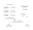
- FIG. 1is a structural view of the system according to the present invention.
- FIG. 2is a flow chart of the method according to the present invention.
- a secrecy system of on-chip data stream of nonvolatile FPGAcomprises a user-defined programmable logic module, a nonvolatile memory module, a programming control module, a programming I/O interface and a user I/O interface.
- the user-defined programmable logic module, the nonvolatile memory module and the programming I/O interfaceare all connected with the programming control module.
- the user I/O interfaceis connected with the user-defined programmable logic module.
- the nonvolatile memory modulecomprises an encryption region unit.
- a full erase operationis only allowed for the nonvolatile memory module under a default state.
- the nonvolatile memory modulegets into an initial state after the full erase operation is finished, and the operation to the nonvolatile memory module is effective only under the initial state.
- the programming control moduleis able to perform a read-write operation to the nonvolatile memory module only by the connecting interface.
- the user-defined programmable logic modulecomprises a SRAM array. Programming data sent by the programming control module is stored in the SRAM array, and the whole user-defined programmable logic module is real-time controlled by the SRAM array.
- the user-defined programmable logic modulecomprises a logic interface.
- the user data of a user data unit of the programming control module obtained from the nonvolatile memory moduleis received by the logic interface.
- the nonvolatile memory modulecomprises several programming logic data units, several user data units and the encryption region unit.
- the programming logic data units, the user data units and the encryption region unitare connected with the programming control module by the connecting interface of the nonvolatile memory module.
- the programming datais sent to the programming logic data units of the nonvolatile memory module by the programming I/O interface via the programming control module.
- the user datais sent to the programming control module from the user I/O interface via the logic interface of the user-defined programmable logic module, and then sent to the user data units of the nonvolatile memory module via the programming control module.
- a decryption method of the secrecy system of on-chip data stream of nonvolatile FPGAcomprises the following steps:
- decryption datais input by a user from a user I/O interface, and gets into a programming control module via a user-defined programmable logic module, and the decryption data input by the user is identified by the programming control module to judge its effectiveness;
- the user data in the nonvolatile memory moduleis initialized and sent to a static memory module of the user by the programming control module.
- the programming data in the nonvolatile memory moduleis loaded into a SRAM array of the user-defined programmable logic module by the programming control module.
- the decryption datacan only be input when the nonvolatile memory module is under the initial state; and the decryption data comprises dynamic data.
- the nonvolatile memory module in the present inventionis configured to only allow the full erase operation. After the full erase operation is finished, the nonvolatile memory module gets into the initial state. Only the operation to the nonvolatile memory module under the initial state is effective, and thereby the encryption region unit is arranged in the nonvolatile memory module. Only the decryption data written into the encryption region unit under the initial state can make the nonvolatile memory module to be readable, so that the decryption of the system is finished, which greatly improves the secrecy precision.
Landscapes
- Engineering & Computer Science (AREA)
- Theoretical Computer Science (AREA)
- Physics & Mathematics (AREA)
- General Engineering & Computer Science (AREA)
- General Physics & Mathematics (AREA)
- Human Computer Interaction (AREA)
- Computer Security & Cryptography (AREA)
- Computer Hardware Design (AREA)
- Software Systems (AREA)
- Microelectronics & Electronic Packaging (AREA)
- Mathematical Physics (AREA)
- Storage Device Security (AREA)
- Read Only Memory (AREA)
Abstract
Description
- The present invention relates to the technical field of data protection of an integrated circuit, and specifically relates to a secrecy system and a decryption method of on-chip data stream of nonvolatile FPGA.
- There are many classification methods of the integrated circuit, which may be classified as Memory, Microprocessor (CPU), Application Specific Integrated Circuits (ASICs) and programmable logic device. The programmable logic device may also be classified as SPLD, CPLD and FPGA. Nowadays the FPGA has become the mainstream. The programmable logic device is called FPGA hereinafter.
- PGA chip is a chip which can input required control program after power is on. FPGA chip is not a stationary circuit, but a chip which can change its function with regard to requirements, and the function can be changed with the input data.
- Based on character of storing programming data, FPGA is classified as volatile FPGA and nonvolatile FPGA. Volatile FPGA usually stores programming data stream using SRAM memory. When a device is powered up, it is typically programmed by an external CPU, or the programming data stream would be loaded automatically by an external nonvolatile memory. After power is off, all the loaded data would be disappeared. The nonvolatile FPGA has retained the programming data stream in the memory itself, so that the nonvolatile FPGA can get into a working state after power is on. After power is off, all the loaded data would be retained.
- Because FPGA is a general device, different users may design their own intellectual property on FPGA, and apply to different technical fields. The intellectual property of the user is stored in the FPGA device in a form of data stream, so that FPGA generates a function that the user requires. If the data stream in the FPGA device is stolen by a lawbreaker, the same FPGA device may be bought, and the stolen data stream is used to program and download the FPGA device, so that user system is totally copied, and the intellectual property of the user may be produced and sold.
- Programming and downloading of the data stream of the volatile FPGA are loaded from a plug-in nonvolatile device, or loaded from an external Central Processing Unit (CPU). Therefore, a hacker may obtain the intellectual property of the user by intercepting the downloaded data externally. The data stream of the nonvolatile FPGA is inside the device, which is more safety relative to the volatile FPGA. However, the hacker may obtain the intellectual property of the user by a special way.
- The problem of data encryption of the nonvolatile memory has been long existed. Data in a memory could be originally read out. Data of this type of memory does not lose after power is off, giving opportunity for a lawbreaker to directly remove the device from a circuit board of a system. The device is put in the lawbreaker's own laboratory to research how to decrypt and then to read out the data.
- In order to solve the contradiction between the memory being readable and the data requiring encryption, Karl M. Guttag and Steve Nussrallah of Texas Instruments Inc. (Texas Instruments Incorporated, Dallas, Tex.) have proposed a method of data encryption of nonvolatile memory as early as 1982, by adding a bit of data as Security Bit. When the memory is required to be read and written normally, the Security Bit is not set (such as “0”). When the memory is required to be encrypted, the Security Bit is set (such as “1”). Any read operations would be automatically prevented by the memory circuit, and then, the only method to convert the Security Bit back into “0” and normally read and write the memory is erasing all data together with the Security Bit. Therefore, the purpose of protecting data of user is reached.
- So far, all the methods of encryption of data stream have one thing in common, that the memory is readable by default. When the data needs to be encrypted, the data becomes unreadable by setting one or more security bits, forming an encryption state. However, if the memory is erasable, only when the security bits and data are all erased, it is revert to a default state, so as to reach the purpose of secrecy.
- With the development of decryption technology, the security bit of a device may be already found out by the exiting inverse design technology. If the security bit is found out and destroyed, the memory may become a readable state, and data therein can be read. Furthermore, if the security bit is set to be only one bit, or the positions of the security bits are relatively concentrated, only the security bits may be just erased by an exact positioning erasing, so the data is easily decrypted.
- A high-safety secrecy system of on-chip data stream of nonvolatile FPGA is provided in present invention, not allowing any other operation except full erase under the condition without decryption data.
- Another object of the present invention is to provide a decryption method of the secrecy system.
- In order to achieve the above technical effect, the technical solution of the present invention is as follows:
- A secrecy system of on-chip data stream of nonvolatile FPGA comprises a user-defined programmable logic module, a nonvolatile memory module, a programming control module, a programming I/O interface and a user I/O interface. The user-defined programmable logic module, the nonvolatile memory module and the programming I/O interface are all connected with the programming control module. The user I/O interface is connected with the user-defined programmable logic module. The nonvolatile memory module comprises an encryption region unit.
- A Full erase operation is only allowed for the nonvolatile memory module under a default state, the nonvolatile memory module gets into an initial state after the full erase operation is finished, and the operation to the nonvolatile memory module is effective only under the initial state.
- Further, only one connecting interface is between the nonvolatile memory module and the programming control module, and the programming control module is able to perform a read-write operation to the nonvolatile memory module only by the connecting interface.
- Further, the user-defined programmable logic module comprises a SRAM array, programming data sent by the programming control module is stored in the SRAM array, and the whole user-defined programmable logic module is real-time controlled by the SRAM array.
- Further, the user-defined programmable logic module comprises a logic interface, and the user data of the user data unit of the programming control module obtained from the nonvolatile memory module is received by the logic interface.
- Further, the nonvolatile memory module comprises several programming logic data units, several user data units and the encryption region unit. The programming logic data units, the user data units and the encryption region unit are connected with the programming control module by the connecting interface of the nonvolatile memory module. The programming data is sent to the programming logic data units of the nonvolatile memory module by the programming I/O interface via the programming control module. The user data is sent to the programming control module from the user I/O interface via the logic interface of the user-defined programmable logic module, and then sent to the user data units of the nonvolatile memory module via the programming control module.
- A decryption method of the secrecy system of on-chip data stream of nonvolatile FPGA comprises following steps:
- S1: powering up the system, and performing a full erase operation to a nonvolatile memory module, so that the nonvolatile memory module gets into an initial state;
- S2: decryption data is input by a user from a user I/O interface, and gets into a programming control module via a user-defined programmable logic module, and the decryption data input by the user is identified by the programming control module to judge its effectiveness;
- S3: effective decryption data is sent to an encryption region unit of the nonvolatile memory module by the programming control module to perform decryption, so that the nonvolatile memory module is in a readable state and then the decryption operation is finished.
- Wherein, after the system is decrypted, the user data in the nonvolatile memory module is initialized to a static memory module of the user by the programming control module.
- Wherein, after decryption of the system is finished, the programming data in the nonvolatile memory module is loaded into a SRAM array of the user-defined programmable logic module by the programming control module.
- Wherein, the decryption data can only be input when the nonvolatile memory module is under the initial state.
- Wherein, the decryption data comprises dynamic data.
- Compared with the existing technologies, the beneficial effects of the technical solution of the present invention include the following by way of example only.
- The nonvolatile memory module in the present invention is configured to only allowed the full erase operation. After the full erase operation is finished, the nonvolatile memory module gets into the initial state. Only the operation to the nonvolatile memory module under the initial state is effective, and thereby the encryption region unit is arranged in the nonvolatile memory module. Only the decryption data written into the encryption region unit under the initial state can make the nonvolatile memory module to be readable, so that the decryption of the system is finished, which greatly improves the secrecy precision.
- The novel features of the present invention are set out with particularity in the appended claims, but the invention will be understood more fully and clearly from the following detailed description of the invention as set forth in the accompanying drawings in which:
FIG. 1 is a structural view of the system according to the present invention; andFIG. 2 is a flow chart of the method according to the present invention.- Accompanying drawings are exclusively for exemplary illustration, and shall not be understood as a limitation to the present invention.
- In order to better illustrate the present embodiment, some components of the accompanying drawings would be eliminated, exaggerated or minimized, but shall not represent the size of a real product.
- For those skilled in the art, it may be understood that some common structures of the accompanying drawings as well as their illustration may be eliminated.
- The technical solution of the present invention will be further illustrated below, in combination with the accompanying drawings and embodiments.
- As shown in
FIG. 1 , a secrecy system of on-chip data stream of nonvolatile FPGA comprises a user-defined programmable logic module, a nonvolatile memory module, a programming control module, a programming I/O interface and a user I/O interface. The user-defined programmable logic module, the nonvolatile memory module and the programming I/O interface are all connected with the programming control module. The user I/O interface is connected with the user-defined programmable logic module. The nonvolatile memory module comprises an encryption region unit. - A full erase operation is only allowed for the nonvolatile memory module under a default state. The nonvolatile memory module gets into an initial state after the full erase operation is finished, and the operation to the nonvolatile memory module is effective only under the initial state.
- Only one connecting interface is between the nonvolatile memory module and the programming control module. The programming control module is able to perform a read-write operation to the nonvolatile memory module only by the connecting interface.
- The user-defined programmable logic module comprises a SRAM array. Programming data sent by the programming control module is stored in the SRAM array, and the whole user-defined programmable logic module is real-time controlled by the SRAM array.
- The user-defined programmable logic module comprises a logic interface. The user data of a user data unit of the programming control module obtained from the nonvolatile memory module is received by the logic interface.
- The nonvolatile memory module comprises several programming logic data units, several user data units and the encryption region unit. The programming logic data units, the user data units and the encryption region unit are connected with the programming control module by the connecting interface of the nonvolatile memory module. The programming data is sent to the programming logic data units of the nonvolatile memory module by the programming I/O interface via the programming control module. The user data is sent to the programming control module from the user I/O interface via the logic interface of the user-defined programmable logic module, and then sent to the user data units of the nonvolatile memory module via the programming control module.
- As shown in
FIG. 2 , a decryption method of the secrecy system of on-chip data stream of nonvolatile FPGA comprises the following steps: - S1: powering up the system, and performing a full erase operation to a nonvolatile memory module, so that the nonvolatile memory module gets into an initial state;
- S2: decryption data is input by a user from a user I/O interface, and gets into a programming control module via a user-defined programmable logic module, and the decryption data input by the user is identified by the programming control module to judge its effectiveness;
- S3: effective decryption data is sent to an encryption region unit of the nonvolatile memory module by the programming control module to perform decryption, so that the nonvolatile memory module is in a readable state and then the decryption operation is finished.
- Wherein, after the system is decrypted, the user data in the nonvolatile memory module is initialized and sent to a static memory module of the user by the programming control module.
- Wherein, after decryption of the system is finished, the programming data in the nonvolatile memory module is loaded into a SRAM array of the user-defined programmable logic module by the programming control module.
- Wherein, the decryption data can only be input when the nonvolatile memory module is under the initial state; and the decryption data comprises dynamic data.
- The nonvolatile memory module in the present invention is configured to only allow the full erase operation. After the full erase operation is finished, the nonvolatile memory module gets into the initial state. Only the operation to the nonvolatile memory module under the initial state is effective, and thereby the encryption region unit is arranged in the nonvolatile memory module. Only the decryption data written into the encryption region unit under the initial state can make the nonvolatile memory module to be readable, so that the decryption of the system is finished, which greatly improves the secrecy precision.
- The same or similar reference signs correspond to the same or similar components.
- The positional relationship in the accompanying drawings is exclusively for exemplary illustration, and shall not be understood as a limitation to the present invention.
- The above embodiments of the present invention are given as examples exclusively used for clearly illustrating the present invention, but not a limitation to the implementations of the present invention. For those ordinarily skilled in the art, other different forms of change or variation can be made based on the above illustration. All implementations should not and could not be exhaustively listed herein. Any modification, equivalent substitution and improvement within the spirit and principle of the present invention, should be all included in the scope of protection of the claims of the present invention.
Claims (10)
Applications Claiming Priority (2)
| Application Number | Priority Date | Filing Date | Title |
|---|---|---|---|
| CN201610534391.4ACN106201352B (en) | 2016-07-07 | 2016-07-07 | The secrecy system and decryption method of non-volatile FPGA on piece data streaming file |
| CN201610534391.4 | 2016-07-07 |
Publications (2)
| Publication Number | Publication Date |
|---|---|
| US20180011803A1true US20180011803A1 (en) | 2018-01-11 |
| US10997088B2 US10997088B2 (en) | 2021-05-04 |
Family
ID=57473925
Family Applications (1)
| Application Number | Title | Priority Date | Filing Date |
|---|---|---|---|
| US15/633,172Active2037-09-08US10997088B2 (en) | 2016-07-07 | 2017-06-26 | Secrecy system and decryption method of on-chip data stream of nonvolatile FPGA |
Country Status (3)
| Country | Link |
|---|---|
| US (1) | US10997088B2 (en) |
| CN (1) | CN106201352B (en) |
| WO (1) | WO2018006556A1 (en) |
Cited By (2)
| Publication number | Priority date | Publication date | Assignee | Title |
|---|---|---|---|---|
| US20190114268A1 (en)* | 2017-10-18 | 2019-04-18 | Gowin Semiconductor Corporation | System level integrated circuit chip |
| US12216773B2 (en)* | 2018-05-22 | 2025-02-04 | Kioxia Corporation | Memory system and method of controlling nonvolatile memory |
Families Citing this family (4)
| Publication number | Priority date | Publication date | Assignee | Title |
|---|---|---|---|---|
| CN106201352B (en)* | 2016-07-07 | 2019-11-29 | 广东高云半导体科技股份有限公司 | The secrecy system and decryption method of non-volatile FPGA on piece data streaming file |
| CN106933752B (en)* | 2017-03-09 | 2019-10-08 | 西安电子科技大学 | A kind of encryption device and method of SRAM type FPGA |
| CN108830114B (en)* | 2018-05-23 | 2020-07-07 | 广东高云半导体科技股份有限公司 | Data processing method and device of nonvolatile memory and storage medium |
| CN111506519B (en)* | 2020-04-22 | 2021-04-27 | 上海安路信息科技股份有限公司 | Method and system for distributing SRAM unit for FPGA code point |
Citations (23)
| Publication number | Priority date | Publication date | Assignee | Title |
|---|---|---|---|---|
| US5603056A (en)* | 1993-09-13 | 1997-02-11 | Kabushiki Kaisha Toshiba | Disk drive control computer and method for rewriting control program in flash EEPROM with serial communication using unassigned pins of SCSI or ATA connector |
| US5845313A (en)* | 1995-07-31 | 1998-12-01 | Lexar | Direct logical block addressing flash memory mass storage architecture |
| US5892712A (en)* | 1996-05-01 | 1999-04-06 | Nvx Corporation | Semiconductor non-volatile latch device including embedded non-volatile elements |
| US20050228980A1 (en)* | 2004-04-08 | 2005-10-13 | Brokish Charles W | Less-secure processors, integrated circuits, wireless communications apparatus, methods and processes of making |
| US20060059373A1 (en)* | 2004-09-10 | 2006-03-16 | International Business Machines Corporation | Integrated circuit chip for encryption and decryption using instructions supplied through a secure interface |
| US7190190B1 (en)* | 2004-01-09 | 2007-03-13 | Altera Corporation | Programmable logic device with on-chip nonvolatile user memory |
| US20070226512A1 (en)* | 2004-06-09 | 2007-09-27 | Koninklijke Philips Electronics, N.V. | Architectures for Privacy Protection of Biometric Templates |
| US20080028187A1 (en)* | 2006-07-28 | 2008-01-31 | Drc Computer Corporation | Configurable Processor Module Accelerator Using A Programmable Logic Device |
| US20090279699A1 (en)* | 2007-08-01 | 2009-11-12 | Mie Noda | Software defined radio device, and method for renewing software, and software defined radio system |
| US20100011261A1 (en)* | 2008-07-08 | 2010-01-14 | International Business Machines Corporation | Verifying Data Integrity of a Non-Volatile Memory System during Data Caching Process |
| US7683660B1 (en)* | 2008-01-31 | 2010-03-23 | Actel Corporation | Programmable logic device with a microcontroller-based control system |
| US20100180065A1 (en)* | 2009-01-09 | 2010-07-15 | Dell Products L.P. | Systems And Methods For Non-Volatile Cache Control |
| US20110138192A1 (en)* | 2009-12-04 | 2011-06-09 | Kocher Paul C | Verifiable, Leak-Resistant Encryption and Decryption |
| US20110302329A1 (en)* | 2010-06-03 | 2011-12-08 | Asad Azam | Embedded Programmable Module for Host Controller Configurability |
| US20130067137A1 (en)* | 2011-09-13 | 2013-03-14 | Michael K. Molloy | Systems and methods for using reserved solid state nonvolatile memory storage capacity for system reduced power state |
| US20130097455A1 (en)* | 2011-06-27 | 2013-04-18 | Huawei Technologies Co., Ltd. | Method and system for implementing interconnection fault tolerance between cpu |
| US20140317612A1 (en)* | 2013-04-17 | 2014-10-23 | American Megatrends, Inc. | Method of fail safe flashing management device and application of the same |
| US20160077979A1 (en)* | 2013-04-29 | 2016-03-17 | Hewlett-Packard Development Company, L. P. | Non-volatile memory to store resettable data |
| US9367701B2 (en)* | 2013-03-08 | 2016-06-14 | Robert Bosch Gmbh | Systems and methods for maintaining integrity and secrecy in untrusted computing platforms |
| US20160202910A1 (en)* | 2015-01-13 | 2016-07-14 | Sandisk Technologies Inc. | Addressing, interleave, wear leveling, and initialization schemes for different chip enables and memory arrays of different types |
| US20160274816A1 (en)* | 2015-03-17 | 2016-09-22 | Gowin Semiconductor Corporation, Ltd. | Programmable Logic Device With On-Chip User Non-Volatile Memory |
| US20170026349A1 (en)* | 2015-07-20 | 2017-01-26 | Schweitzer Engineering Laboratories, Inc. | Communication device for implementing selective encryption in a software defined network |
| US20170208047A1 (en)* | 2016-01-20 | 2017-07-20 | Medicom Technologies, Inc. | Methods and systems for providing secure and auditable transfer of encrypted data between remote locations |
Family Cites Families (22)
| Publication number | Priority date | Publication date | Assignee | Title |
|---|---|---|---|---|
| US4521852A (en)* | 1982-06-30 | 1985-06-04 | Texas Instruments Incorporated | Data processing device formed on a single semiconductor substrate having secure memory |
| US6522694B1 (en)* | 1998-10-09 | 2003-02-18 | Matsushita Electric Industrial Co., Ltd. | Programmable filter for removing stuffing bits from an MPEG-2 bit-stream |
| US6331784B1 (en)* | 2000-07-28 | 2001-12-18 | Atmel Corporation | Secure programmable logic device |
| US7162644B1 (en)* | 2002-03-29 | 2007-01-09 | Xilinx, Inc. | Methods and circuits for protecting proprietary configuration data for programmable logic devices |
| US7878902B2 (en)* | 2003-07-16 | 2011-02-01 | Igt | Secured verification of configuration data for field programmable gate array devices |
| US20060059369A1 (en)* | 2004-09-10 | 2006-03-16 | International Business Machines Corporation | Circuit chip for cryptographic processing having a secure interface to an external memory |
| US7368935B2 (en)* | 2005-10-18 | 2008-05-06 | Honeywell International Inc. | Tamper response system for integrated circuits |
| US8019938B2 (en)* | 2006-12-06 | 2011-09-13 | Fusion-I0, Inc. | Apparatus, system, and method for solid-state storage as cache for high-capacity, non-volatile storage |
| WO2009024913A2 (en)* | 2007-08-22 | 2009-02-26 | Intrinsic Id Bv | Identification of devices using physically unclonable functions |
| US20090125726A1 (en)* | 2007-11-14 | 2009-05-14 | Mcm Portfolio Llc | Method and Apparatus of Providing the Security and Error Correction Capability for Memory Storage Devices |
| CN201142071Y (en)* | 2007-12-04 | 2008-10-29 | 上海海尔集成电路有限公司 | 8-digit flash memory microcontroller |
| CN102053926A (en)* | 2009-10-30 | 2011-05-11 | 鸿富锦精密工业(深圳)有限公司 | Storage device and data security control method thereof |
| CN101835146A (en)* | 2010-04-12 | 2010-09-15 | 东南大学 | End-to-end encryption device and method for third-generation mobile network mobile phone voice |
| US8892837B2 (en)* | 2011-02-22 | 2014-11-18 | Altera Corporation | Integrated circuit with tamper-detection and self-erase mechanisms |
| CN102651686A (en)* | 2011-02-23 | 2012-08-29 | 上海华虹集成电路有限责任公司 | On-line programmable identity authentication method for singlechip |
| KR101303278B1 (en)* | 2011-12-14 | 2013-09-04 | 한국전자통신연구원 | FPGA apparatus and method for protecting bitstream |
| US10318158B2 (en)* | 2012-05-17 | 2019-06-11 | Brilliant Points, Inc. | System and method for digital signaling and digital storage |
| WO2014199678A1 (en)* | 2013-06-12 | 2014-12-18 | 日本電気株式会社 | Configuration control system and configuration control method |
| CN103413097B (en)* | 2013-07-15 | 2017-02-15 | 北京华大信安科技有限公司 | Encryption method, encryption device and security chip |
| US9940483B2 (en)* | 2016-01-25 | 2018-04-10 | Raytheon Company | Firmware security interface for field programmable gate arrays |
| US10725677B2 (en)* | 2016-02-19 | 2020-07-28 | Sandisk Technologies Llc | Systems and methods for efficient power state transitions |
| CN106201352B (en)* | 2016-07-07 | 2019-11-29 | 广东高云半导体科技股份有限公司 | The secrecy system and decryption method of non-volatile FPGA on piece data streaming file |
- 2016
- 2016-07-07CNCN201610534391.4Apatent/CN106201352B/enactiveActive
- 2016-12-22WOPCT/CN2016/111406patent/WO2018006556A1/ennot_activeCeased
- 2017
- 2017-06-26USUS15/633,172patent/US10997088B2/enactiveActive
Patent Citations (23)
| Publication number | Priority date | Publication date | Assignee | Title |
|---|---|---|---|---|
| US5603056A (en)* | 1993-09-13 | 1997-02-11 | Kabushiki Kaisha Toshiba | Disk drive control computer and method for rewriting control program in flash EEPROM with serial communication using unassigned pins of SCSI or ATA connector |
| US5845313A (en)* | 1995-07-31 | 1998-12-01 | Lexar | Direct logical block addressing flash memory mass storage architecture |
| US5892712A (en)* | 1996-05-01 | 1999-04-06 | Nvx Corporation | Semiconductor non-volatile latch device including embedded non-volatile elements |
| US7190190B1 (en)* | 2004-01-09 | 2007-03-13 | Altera Corporation | Programmable logic device with on-chip nonvolatile user memory |
| US20050228980A1 (en)* | 2004-04-08 | 2005-10-13 | Brokish Charles W | Less-secure processors, integrated circuits, wireless communications apparatus, methods and processes of making |
| US20070226512A1 (en)* | 2004-06-09 | 2007-09-27 | Koninklijke Philips Electronics, N.V. | Architectures for Privacy Protection of Biometric Templates |
| US20060059373A1 (en)* | 2004-09-10 | 2006-03-16 | International Business Machines Corporation | Integrated circuit chip for encryption and decryption using instructions supplied through a secure interface |
| US20080028187A1 (en)* | 2006-07-28 | 2008-01-31 | Drc Computer Corporation | Configurable Processor Module Accelerator Using A Programmable Logic Device |
| US20090279699A1 (en)* | 2007-08-01 | 2009-11-12 | Mie Noda | Software defined radio device, and method for renewing software, and software defined radio system |
| US7683660B1 (en)* | 2008-01-31 | 2010-03-23 | Actel Corporation | Programmable logic device with a microcontroller-based control system |
| US20100011261A1 (en)* | 2008-07-08 | 2010-01-14 | International Business Machines Corporation | Verifying Data Integrity of a Non-Volatile Memory System during Data Caching Process |
| US20100180065A1 (en)* | 2009-01-09 | 2010-07-15 | Dell Products L.P. | Systems And Methods For Non-Volatile Cache Control |
| US20110138192A1 (en)* | 2009-12-04 | 2011-06-09 | Kocher Paul C | Verifiable, Leak-Resistant Encryption and Decryption |
| US20110302329A1 (en)* | 2010-06-03 | 2011-12-08 | Asad Azam | Embedded Programmable Module for Host Controller Configurability |
| US20130097455A1 (en)* | 2011-06-27 | 2013-04-18 | Huawei Technologies Co., Ltd. | Method and system for implementing interconnection fault tolerance between cpu |
| US20130067137A1 (en)* | 2011-09-13 | 2013-03-14 | Michael K. Molloy | Systems and methods for using reserved solid state nonvolatile memory storage capacity for system reduced power state |
| US9367701B2 (en)* | 2013-03-08 | 2016-06-14 | Robert Bosch Gmbh | Systems and methods for maintaining integrity and secrecy in untrusted computing platforms |
| US20140317612A1 (en)* | 2013-04-17 | 2014-10-23 | American Megatrends, Inc. | Method of fail safe flashing management device and application of the same |
| US20160077979A1 (en)* | 2013-04-29 | 2016-03-17 | Hewlett-Packard Development Company, L. P. | Non-volatile memory to store resettable data |
| US20160202910A1 (en)* | 2015-01-13 | 2016-07-14 | Sandisk Technologies Inc. | Addressing, interleave, wear leveling, and initialization schemes for different chip enables and memory arrays of different types |
| US20160274816A1 (en)* | 2015-03-17 | 2016-09-22 | Gowin Semiconductor Corporation, Ltd. | Programmable Logic Device With On-Chip User Non-Volatile Memory |
| US20170026349A1 (en)* | 2015-07-20 | 2017-01-26 | Schweitzer Engineering Laboratories, Inc. | Communication device for implementing selective encryption in a software defined network |
| US20170208047A1 (en)* | 2016-01-20 | 2017-07-20 | Medicom Technologies, Inc. | Methods and systems for providing secure and auditable transfer of encrypted data between remote locations |
Cited By (3)
| Publication number | Priority date | Publication date | Assignee | Title |
|---|---|---|---|---|
| US20190114268A1 (en)* | 2017-10-18 | 2019-04-18 | Gowin Semiconductor Corporation | System level integrated circuit chip |
| US11157421B2 (en)* | 2017-10-18 | 2021-10-26 | Gowin Semiconductor Corporation | System level integrated circuit chip |
| US12216773B2 (en)* | 2018-05-22 | 2025-02-04 | Kioxia Corporation | Memory system and method of controlling nonvolatile memory |
Also Published As
| Publication number | Publication date |
|---|---|
| CN106201352B (en) | 2019-11-29 |
| US10997088B2 (en) | 2021-05-04 |
| WO2018006556A1 (en) | 2018-01-11 |
| CN106201352A (en) | 2016-12-07 |
Similar Documents
| Publication | Publication Date | Title |
|---|---|---|
| US10997088B2 (en) | Secrecy system and decryption method of on-chip data stream of nonvolatile FPGA | |
| US9094190B2 (en) | Method of managing key for secure storage of data and apparatus therefor | |
| US8572410B1 (en) | Virtualized protected storage | |
| JP6585153B2 (en) | A device using flash memory to store important or sensitive technical information and other data | |
| US20190384938A1 (en) | Storage apparatus and method for address scrambling | |
| US20140122903A1 (en) | Semiconductor device and encryption key writing method | |
| US20080155272A1 (en) | Semiconductor integrated circuit device, program delivery method, and program delivery system | |
| CN101241534A (en) | Semiconductor device with encryption part or external interface and content reproduction method | |
| US7752407B1 (en) | Security RAM block | |
| US7761654B2 (en) | System and method of utilizing off-chip memory | |
| JP2014194734A (en) | Data storage device and data protection method | |
| US20170039397A1 (en) | Encryption/decryption apparatus, controller and encryption key protection method | |
| US10505927B2 (en) | Memory device and host device | |
| KR20130067849A (en) | Fpga apparatus and method for protecting bitstream | |
| CN112131537A (en) | Method for encrypting and decrypting ZYNQ chip program image file | |
| WO2015176531A1 (en) | Terminal data writing and reading methods and devices | |
| US20150227755A1 (en) | Encryption and decryption methods of a mobile storage on a file-by-file basis | |
| US20190377878A1 (en) | Secure Drive | |
| CN100405335C (en) | Memory information protection system, semiconductor memory and method for protecting memory information | |
| JP2019504519A (en) | Lifecycle encryption management | |
| CN101950345B (en) | Hardware decryption-based high-reliability terminal equipment and working method thereof | |
| JP6203532B2 (en) | Semiconductor memory device and data processing system | |
| KR102295470B1 (en) | Secure usb dongle for usb memory without security | |
| US20200192824A1 (en) | Security memory device and operation method thereof | |
| KR20150101232A (en) | Method of operating storage device including nonvolatile memory and memory controller |
Legal Events
| Date | Code | Title | Description |
|---|---|---|---|
| AS | Assignment | Owner name:GOWIN SEMICONDUCTOR CORPORATION, LTD., CHINA Free format text:ASSIGNMENT OF ASSIGNORS INTEREST;ASSIGNORS:KOW, SAN-TA;ZHU, JINGHUI;CHOPPERLA, DIWAKAR;REEL/FRAME:042818/0069 Effective date:20170623 | |
| STPP | Information on status: patent application and granting procedure in general | Free format text:NON FINAL ACTION MAILED | |
| STPP | Information on status: patent application and granting procedure in general | Free format text:RESPONSE TO NON-FINAL OFFICE ACTION ENTERED AND FORWARDED TO EXAMINER | |
| STPP | Information on status: patent application and granting procedure in general | Free format text:FINAL REJECTION MAILED | |
| STPP | Information on status: patent application and granting procedure in general | Free format text:RESPONSE AFTER FINAL ACTION FORWARDED TO EXAMINER | |
| STPP | Information on status: patent application and granting procedure in general | Free format text:ADVISORY ACTION MAILED | |
| STPP | Information on status: patent application and granting procedure in general | Free format text:DOCKETED NEW CASE - READY FOR EXAMINATION | |
| STPP | Information on status: patent application and granting procedure in general | Free format text:NOTICE OF ALLOWANCE MAILED -- APPLICATION RECEIVED IN OFFICE OF PUBLICATIONS | |
| STPP | Information on status: patent application and granting procedure in general | Free format text:PUBLICATIONS -- ISSUE FEE PAYMENT VERIFIED | |
| STCF | Information on status: patent grant | Free format text:PATENTED CASE | |
| FEPP | Fee payment procedure | Free format text:MAINTENANCE FEE REMINDER MAILED (ORIGINAL EVENT CODE: REM.); ENTITY STATUS OF PATENT OWNER: SMALL ENTITY | |
| FEPP | Fee payment procedure | Free format text:SURCHARGE FOR LATE PAYMENT, SMALL ENTITY (ORIGINAL EVENT CODE: M2554); ENTITY STATUS OF PATENT OWNER: SMALL ENTITY | |
| MAFP | Maintenance fee payment | Free format text:PAYMENT OF MAINTENANCE FEE, 4TH YR, SMALL ENTITY (ORIGINAL EVENT CODE: M2551); ENTITY STATUS OF PATENT OWNER: SMALL ENTITY Year of fee payment:4 |