US20180005814A1 - Selective atomic layer deposition with post-dose treatment - Google Patents
Selective atomic layer deposition with post-dose treatmentDownload PDFInfo
- Publication number
- US20180005814A1 US20180005814A1US15/201,221US201615201221AUS2018005814A1US 20180005814 A1US20180005814 A1US 20180005814A1US 201615201221 AUS201615201221 AUS 201615201221AUS 2018005814 A1US2018005814 A1US 2018005814A1
- Authority
- US
- United States
- Prior art keywords
- silicon
- post
- plasma
- substrate
- dose treatment
- Prior art date
- Legal status (The legal status is an assumption and is not a legal conclusion. Google has not performed a legal analysis and makes no representation as to the accuracy of the status listed.)
- Granted
Links
- 238000011282treatmentMethods0.000titleclaimsabstractdescription98
- 238000000231atomic layer depositionMethods0.000titleabstractdescription41
- 238000000034methodMethods0.000claimsabstractdescription200
- 239000000758substrateSubstances0.000claimsabstractdescription170
- 239000002243precursorSubstances0.000claimsabstractdescription137
- XUIMIQQOPSSXEZ-UHFFFAOYSA-NSiliconChemical compound[Si]XUIMIQQOPSSXEZ-UHFFFAOYSA-N0.000claimsabstractdescription93
- 229910052710siliconInorganic materials0.000claimsabstractdescription93
- 239000010703siliconSubstances0.000claimsabstractdescription92
- 230000001590oxidative effectEffects0.000claimsabstractdescription27
- 230000005855radiationEffects0.000claimsabstractdescription8
- 230000008569processEffects0.000claimsdescription152
- 239000007789gasSubstances0.000claimsdescription97
- 239000000376reactantSubstances0.000claimsdescription85
- XKRFYHLGVUSROY-UHFFFAOYSA-NArgonChemical compound[Ar]XKRFYHLGVUSROY-UHFFFAOYSA-N0.000claimsdescription54
- IJGRMHOSHXDMSA-UHFFFAOYSA-NAtomic nitrogenChemical compoundN#NIJGRMHOSHXDMSA-UHFFFAOYSA-N0.000claimsdescription53
- NJPPVKZQTLUDBO-UHFFFAOYSA-NnovaluronChemical compoundC1=C(Cl)C(OC(F)(F)C(OC(F)(F)F)F)=CC=C1NC(=O)NC(=O)C1=C(F)C=CC=C1FNJPPVKZQTLUDBO-UHFFFAOYSA-N0.000claimsdescription45
- VYPSYNLAJGMNEJ-UHFFFAOYSA-NSilicium dioxideChemical compoundO=[Si]=OVYPSYNLAJGMNEJ-UHFFFAOYSA-N0.000claimsdescription44
- 229910052814silicon oxideInorganic materials0.000claimsdescription42
- 238000012545processingMethods0.000claimsdescription38
- 239000001301oxygenSubstances0.000claimsdescription37
- 229910052760oxygenInorganic materials0.000claimsdescription37
- QVGXLLKOCUKJST-UHFFFAOYSA-Natomic oxygenChemical compound[O]QVGXLLKOCUKJST-UHFFFAOYSA-N0.000claimsdescription35
- 229910052786argonInorganic materials0.000claimsdescription27
- 229910052757nitrogenInorganic materials0.000claimsdescription27
- QGZKDVFQNNGYKY-UHFFFAOYSA-NAmmoniaChemical compoundNQGZKDVFQNNGYKY-UHFFFAOYSA-N0.000claimsdescription24
- 229910052581Si3N4Inorganic materials0.000claimsdescription12
- 229910021529ammoniaInorganic materials0.000claimsdescription12
- HQVNEWCFYHHQES-UHFFFAOYSA-Nsilicon nitrideChemical compoundN12[Si]34N5[Si]62N3[Si]51N64HQVNEWCFYHHQES-UHFFFAOYSA-N0.000claimsdescription12
- 229910052734heliumInorganic materials0.000claimsdescription9
- 239000001307heliumSubstances0.000claimsdescription9
- SWQJXJOGLNCZEY-UHFFFAOYSA-Nhelium atomChemical compound[He]SWQJXJOGLNCZEY-UHFFFAOYSA-N0.000claimsdescription9
- 239000001257hydrogenSubstances0.000claimsdescription9
- 229910052739hydrogenInorganic materials0.000claimsdescription9
- 125000004435hydrogen atomChemical class[H]*0.000claimsdescription4
- 229910010271silicon carbideInorganic materials0.000claimsdescription4
- 230000008878couplingEffects0.000claimsdescription3
- 238000010168coupling processMethods0.000claimsdescription3
- 238000005859coupling reactionMethods0.000claimsdescription3
- HBMJWWWQQXIZIP-UHFFFAOYSA-Nsilicon carbideChemical compound[Si+]#[C-]HBMJWWWQQXIZIP-UHFFFAOYSA-N0.000claimsdescription3
- 238000000151depositionMethods0.000abstractdescription88
- 210000002381plasmaAnatomy0.000description161
- 239000010408filmSubstances0.000description88
- 230000008021depositionEffects0.000description79
- 238000010926purgeMethods0.000description50
- 239000010410layerSubstances0.000description37
- 235000012431wafersNutrition0.000description31
- 239000012159carrier gasSubstances0.000description22
- 239000007788liquidSubstances0.000description17
- 238000004519manufacturing processMethods0.000description15
- 239000000463materialSubstances0.000description15
- 239000004065semiconductorSubstances0.000description15
- 230000001276controlling effectEffects0.000description11
- 238000002156mixingMethods0.000description11
- 230000008016vaporizationEffects0.000description10
- 238000002474experimental methodMethods0.000description9
- 239000000203mixtureSubstances0.000description9
- -1silicon nitridesChemical class0.000description9
- 238000009834vaporizationMethods0.000description9
- 238000006243chemical reactionMethods0.000description8
- 150000001875compoundsChemical class0.000description8
- 238000001179sorption measurementMethods0.000description8
- 230000015572biosynthetic processEffects0.000description7
- OKTJSMMVPCPJKN-UHFFFAOYSA-NCarbonChemical compound[C]OKTJSMMVPCPJKN-UHFFFAOYSA-N0.000description6
- 238000010586diagramMethods0.000description6
- 150000002431hydrogenChemical class0.000description6
- QJGQUHMNIGDVPM-UHFFFAOYSA-Nnitrogen groupChemical group[N]QJGQUHMNIGDVPM-UHFFFAOYSA-N0.000description6
- 230000009467reductionEffects0.000description6
- FZHAPNGMFPVSLP-UHFFFAOYSA-NsilanamineChemical compound[SiH3]NFZHAPNGMFPVSLP-UHFFFAOYSA-N0.000description6
- 239000011800void materialSubstances0.000description6
- KRHYYFGTRYWZRS-UHFFFAOYSA-NFluoraneChemical compoundFKRHYYFGTRYWZRS-UHFFFAOYSA-N0.000description5
- 150000001412aminesChemical class0.000description5
- 229910052799carbonInorganic materials0.000description5
- 230000007423decreaseEffects0.000description5
- 238000000280densificationMethods0.000description5
- 238000011065in-situ storageMethods0.000description5
- 239000002184metalSubstances0.000description5
- 229910052751metalInorganic materials0.000description5
- 238000012546transferMethods0.000description5
- 239000003153chemical reaction reagentSubstances0.000description4
- 238000005229chemical vapour depositionMethods0.000description4
- 238000009792diffusion processMethods0.000description4
- 238000009826distributionMethods0.000description4
- 230000002045lasting effectEffects0.000description4
- 239000007800oxidant agentSubstances0.000description4
- 150000003254radicalsChemical class0.000description4
- 229920006395saturated elastomerPolymers0.000description4
- ROSDSFDQCJNGOL-UHFFFAOYSA-NDimethylamineChemical compoundCNCROSDSFDQCJNGOL-UHFFFAOYSA-N0.000description3
- BLRPTPMANUNPDV-UHFFFAOYSA-NSilaneChemical compound[SiH4]BLRPTPMANUNPDV-UHFFFAOYSA-N0.000description3
- 238000001636atomic emission spectroscopyMethods0.000description3
- 239000006227byproductSubstances0.000description3
- KOPOQZFJUQMUML-UHFFFAOYSA-NchlorosilaneChemical classCl[SiH3]KOPOQZFJUQMUML-UHFFFAOYSA-N0.000description3
- UAOMVDZJSHZZME-UHFFFAOYSA-NdiisopropylamineChemical compoundCC(C)NC(C)CUAOMVDZJSHZZME-UHFFFAOYSA-N0.000description3
- 238000005530etchingMethods0.000description3
- 239000011261inert gasSubstances0.000description3
- 150000002500ionsChemical class0.000description3
- QPJSUIGXIBEQAC-UHFFFAOYSA-Nn-(2,4-dichloro-5-propan-2-yloxyphenyl)acetamideChemical compoundCC(C)OC1=CC(NC(C)=O)=C(Cl)C=C1ClQPJSUIGXIBEQAC-UHFFFAOYSA-N0.000description3
- 150000004767nitridesChemical class0.000description3
- 229920002120photoresistant polymerPolymers0.000description3
- 238000003860storageMethods0.000description3
- 238000011144upstream manufacturingMethods0.000description3
- CURLTUGMZLYLDI-UHFFFAOYSA-NCarbon dioxideChemical compoundO=C=OCURLTUGMZLYLDI-UHFFFAOYSA-N0.000description2
- 239000005046ChlorosilaneSubstances0.000description2
- QUSNBJAOOMFDIB-UHFFFAOYSA-NEthylamineChemical compoundCCNQUSNBJAOOMFDIB-UHFFFAOYSA-N0.000description2
- OAKJQQAXSVQMHS-UHFFFAOYSA-NHydrazineChemical compoundNNOAKJQQAXSVQMHS-UHFFFAOYSA-N0.000description2
- BAVYZALUXZFZLV-UHFFFAOYSA-NMethylamineChemical compoundNCBAVYZALUXZFZLV-UHFFFAOYSA-N0.000description2
- MWUXSHHQAYIFBG-UHFFFAOYSA-NNitric oxideChemical compoundO=[N]MWUXSHHQAYIFBG-UHFFFAOYSA-N0.000description2
- GQPLMRYTRLFLPF-UHFFFAOYSA-NNitrous OxideChemical compound[O-][N+]#NGQPLMRYTRLFLPF-UHFFFAOYSA-N0.000description2
- 229910003828SiH3Inorganic materials0.000description2
- RAHZWNYVWXNFOC-UHFFFAOYSA-NSulphur dioxideChemical compoundO=S=ORAHZWNYVWXNFOC-UHFFFAOYSA-N0.000description2
- 230000004888barrier functionEffects0.000description2
- 230000015556catabolic processEffects0.000description2
- 238000004891communicationMethods0.000description2
- 238000005137deposition processMethods0.000description2
- 238000011049fillingMethods0.000description2
- 150000004820halidesChemical class0.000description2
- 238000010438heat treatmentMethods0.000description2
- BMFVGAAISNGQNM-UHFFFAOYSA-NisopentylamineChemical compoundCC(C)CCNBMFVGAAISNGQNM-UHFFFAOYSA-N0.000description2
- 238000001459lithographyMethods0.000description2
- 238000005259measurementMethods0.000description2
- 230000001404mediated effectEffects0.000description2
- 125000004433nitrogen atomChemical groupN*0.000description2
- 230000003647oxidationEffects0.000description2
- 238000007254oxidation reactionMethods0.000description2
- 239000002245particleSubstances0.000description2
- 238000005240physical vapour depositionMethods0.000description2
- 238000000678plasma activationMethods0.000description2
- 238000009428plumbingMethods0.000description2
- 238000011112process operationMethods0.000description2
- 238000012163sequencing techniqueMethods0.000description2
- 229910000077silaneInorganic materials0.000description2
- 239000012686silicon precursorSubstances0.000description2
- GETQZCLCWQTVFV-UHFFFAOYSA-NtrimethylamineChemical compoundCN(C)CGETQZCLCWQTVFV-UHFFFAOYSA-N0.000description2
- JZKAJIFHBZJCAI-UHFFFAOYSA-N1,2-ditert-butylhydrazineChemical compoundCC(C)(C)NNC(C)(C)CJZKAJIFHBZJCAI-UHFFFAOYSA-N0.000description1
- BEEYLGLWYXWFAG-UHFFFAOYSA-N2-aminosilyl-2-methylpropaneChemical compoundCC(C)(C)[SiH2]NBEEYLGLWYXWFAG-UHFFFAOYSA-N0.000description1
- MAYUMUDTQDNZBD-UHFFFAOYSA-N2-chloroethylsilaneChemical compound[SiH3]CCClMAYUMUDTQDNZBD-UHFFFAOYSA-N0.000description1
- VUGMARFZKDASCX-UHFFFAOYSA-N2-methyl-N-silylpropan-2-amineChemical compoundCC(C)(C)N[SiH3]VUGMARFZKDASCX-UHFFFAOYSA-N0.000description1
- GELMWIVBBPAMIO-UHFFFAOYSA-N2-methylbutan-2-amineChemical compoundCCC(C)(C)NGELMWIVBBPAMIO-UHFFFAOYSA-N0.000description1
- MNTMWHBQGOKGDD-UHFFFAOYSA-N3-methylbutylsilaneChemical compoundCC(C)CC[SiH3]MNTMWHBQGOKGDD-UHFFFAOYSA-N0.000description1
- MGWGWNFMUOTEHG-UHFFFAOYSA-N4-(3,5-dimethylphenyl)-1,3-thiazol-2-amineChemical compoundCC1=CC(C)=CC(C=2N=C(N)SC=2)=C1MGWGWNFMUOTEHG-UHFFFAOYSA-N0.000description1
- UGFAIRIUMAVXCW-UHFFFAOYSA-NCarbon monoxideChemical compound[O+]#[C-]UGFAIRIUMAVXCW-UHFFFAOYSA-N0.000description1
- HTJDQJBWANPRPF-UHFFFAOYSA-NCyclopropylamineChemical compoundNC1CC1HTJDQJBWANPRPF-UHFFFAOYSA-N0.000description1
- MYMOFIZGZYHOMD-UHFFFAOYSA-NDioxygenChemical compoundO=OMYMOFIZGZYHOMD-UHFFFAOYSA-N0.000description1
- 229910003946H3SiInorganic materials0.000description1
- UFHFLCQGNIYNRP-UHFFFAOYSA-NHydrogenChemical compound[H][H]UFHFLCQGNIYNRP-UHFFFAOYSA-N0.000description1
- AVXURJPOCDRRFD-UHFFFAOYSA-NHydroxylamineChemical compoundONAVXURJPOCDRRFD-UHFFFAOYSA-N0.000description1
- CBENFWSGALASAD-UHFFFAOYSA-NOzoneChemical compound[O-][O+]=OCBENFWSGALASAD-UHFFFAOYSA-N0.000description1
- 238000003848UV Light-CuringMethods0.000description1
- XMIJDTGORVPYLW-UHFFFAOYSA-N[SiH2]Chemical compound[SiH2]XMIJDTGORVPYLW-UHFFFAOYSA-N0.000description1
- 238000001994activationMethods0.000description1
- 230000004913activationEffects0.000description1
- 150000001448anilinesChemical class0.000description1
- 238000013459approachMethods0.000description1
- 238000003491arrayMethods0.000description1
- 125000003118aryl groupChemical group0.000description1
- 150000003939benzylaminesChemical class0.000description1
- VQPFDLRNOCQMSN-UHFFFAOYSA-NbromosilaneChemical classBr[SiH3]VQPFDLRNOCQMSN-UHFFFAOYSA-N0.000description1
- AUOLYXZHVVMFPD-UHFFFAOYSA-Nbutan-2-yl(chloro)silaneChemical compoundCCC(C)[SiH2]ClAUOLYXZHVVMFPD-UHFFFAOYSA-N0.000description1
- VBLDUBUUQYXSCG-UHFFFAOYSA-Nbutan-2-ylsilaneChemical compoundCCC(C)[SiH3]VBLDUBUUQYXSCG-UHFFFAOYSA-N0.000description1
- 229910002092carbon dioxideInorganic materials0.000description1
- 239000001569carbon dioxideSubstances0.000description1
- 229910002091carbon monoxideInorganic materials0.000description1
- 230000008859changeEffects0.000description1
- CRIVIYPBVUGWSC-UHFFFAOYSA-Nchloro(propan-2-yl)silaneChemical compoundCC(C)[SiH2]ClCRIVIYPBVUGWSC-UHFFFAOYSA-N0.000description1
- KIGALSBMRYYLFJ-UHFFFAOYSA-Nchloro-(2,3-dimethylbutan-2-yl)-dimethylsilaneChemical compoundCC(C)C(C)(C)[Si](C)(C)ClKIGALSBMRYYLFJ-UHFFFAOYSA-N0.000description1
- YGHUUVGIRWMJGE-UHFFFAOYSA-NchlorodimethylsilaneChemical compoundC[SiH](C)ClYGHUUVGIRWMJGE-UHFFFAOYSA-N0.000description1
- AZFVLHQDIIJLJG-UHFFFAOYSA-NchloromethylsilaneChemical compound[SiH3]CClAZFVLHQDIIJLJG-UHFFFAOYSA-N0.000description1
- 238000004140cleaningMethods0.000description1
- 230000003750conditioning effectEffects0.000description1
- 239000004020conductorSubstances0.000description1
- 238000007796conventional methodMethods0.000description1
- 238000001816coolingMethods0.000description1
- 238000001723curingMethods0.000description1
- KZZKOVLJUKWSKX-UHFFFAOYSA-NcyclobutanamineChemical compoundNC1CCC1KZZKOVLJUKWSKX-UHFFFAOYSA-N0.000description1
- 238000006731degradation reactionMethods0.000description1
- 230000000593degrading effectEffects0.000description1
- UWGIJJRGSGDBFJ-UHFFFAOYSA-NdichloromethylsilaneChemical compound[SiH3]C(Cl)ClUWGIJJRGSGDBFJ-UHFFFAOYSA-N0.000description1
- MROCJMGDEKINLD-UHFFFAOYSA-NdichlorosilaneChemical compoundCl[SiH2]ClMROCJMGDEKINLD-UHFFFAOYSA-N0.000description1
- 239000003989dielectric materialSubstances0.000description1
- UCXUKTLCVSGCNR-UHFFFAOYSA-NdiethylsilaneChemical compoundCC[SiH2]CCUCXUKTLCVSGCNR-UHFFFAOYSA-N0.000description1
- 229940043279diisopropylamineDrugs0.000description1
- UBHZUDXTHNMNLD-UHFFFAOYSA-NdimethylsilaneChemical compoundC[SiH2]CUBHZUDXTHNMNLD-UHFFFAOYSA-N0.000description1
- 229910001873dinitrogenInorganic materials0.000description1
- 229910001882dioxygenInorganic materials0.000description1
- PZPGRFITIJYNEJ-UHFFFAOYSA-NdisilaneChemical compound[SiH3][SiH3]PZPGRFITIJYNEJ-UHFFFAOYSA-N0.000description1
- TXKMVPPZCYKFAC-UHFFFAOYSA-Ndisulfur monoxideInorganic materialsO=S=STXKMVPPZCYKFAC-UHFFFAOYSA-N0.000description1
- OGWXFZNXPZTBST-UHFFFAOYSA-Nditert-butyl(chloro)silaneChemical compoundCC(C)(C)[SiH](Cl)C(C)(C)COGWXFZNXPZTBST-UHFFFAOYSA-N0.000description1
- LFLMSLJSSVNEJH-UHFFFAOYSA-Nditert-butyl(silyl)silaneChemical compoundCC(C)(C)[SiH]([SiH3])C(C)(C)CLFLMSLJSSVNEJH-UHFFFAOYSA-N0.000description1
- JTGAUXSVQKWNHO-UHFFFAOYSA-Nditert-butylsiliconChemical compoundCC(C)(C)[Si]C(C)(C)CJTGAUXSVQKWNHO-UHFFFAOYSA-N0.000description1
- 239000002019doping agentSubstances0.000description1
- 230000000694effectsEffects0.000description1
- 238000005531etching kineticMethods0.000description1
- KCWYOFZQRFCIIE-UHFFFAOYSA-NethylsilaneChemical compoundCC[SiH3]KCWYOFZQRFCIIE-UHFFFAOYSA-N0.000description1
- 238000001704evaporationMethods0.000description1
- 230000008020evaporationEffects0.000description1
- 239000012530fluidSubstances0.000description1
- 239000003574free electronSubstances0.000description1
- 229910052736halogenInorganic materials0.000description1
- 125000005843halogen groupChemical group0.000description1
- 150000002367halogensChemical class0.000description1
- 125000005842heteroatomChemical group0.000description1
- 229930195733hydrocarbonNatural products0.000description1
- 150000002430hydrocarbonsChemical class0.000description1
- 125000002887hydroxy groupChemical group[H]O*0.000description1
- 239000012535impuritySubstances0.000description1
- 238000002347injectionMethods0.000description1
- 239000007924injectionSubstances0.000description1
- IDIOJRGTRFRIJL-UHFFFAOYSA-NiodosilaneChemical classI[SiH3]IDIOJRGTRFRIJL-UHFFFAOYSA-N0.000description1
- 238000010849ion bombardmentMethods0.000description1
- 238000005468ion implantationMethods0.000description1
- JJWLVOIRVHMVIS-UHFFFAOYSA-NisopropylamineChemical compoundCC(C)NJJWLVOIRVHMVIS-UHFFFAOYSA-N0.000description1
- 239000012705liquid precursorSubstances0.000description1
- 230000007246mechanismEffects0.000description1
- 150000001247metal acetylidesChemical class0.000description1
- 229910044991metal oxideInorganic materials0.000description1
- 150000004706metal oxidesChemical class0.000description1
- 150000002739metalsChemical class0.000description1
- IFVRUKGTKXWWQF-UHFFFAOYSA-NmethylaminosiliconChemical compoundCN[Si]IFVRUKGTKXWWQF-UHFFFAOYSA-N0.000description1
- UIUXUFNYAYAMOE-UHFFFAOYSA-NmethylsilaneChemical compound[SiH3]CUIUXUFNYAYAMOE-UHFFFAOYSA-N0.000description1
- 238000012986modificationMethods0.000description1
- 230000004048modificationEffects0.000description1
- 230000004001molecular interactionEffects0.000description1
- 238000012544monitoring processMethods0.000description1
- ULWOJODHECIZAU-UHFFFAOYSA-Nn,n-diethylpropan-2-amineChemical compoundCCN(CC)C(C)CULWOJODHECIZAU-UHFFFAOYSA-N0.000description1
- VYIRVGYSUZPNLF-UHFFFAOYSA-Nn-(tert-butylamino)silyl-2-methylpropan-2-amineChemical compoundCC(C)(C)N[SiH2]NC(C)(C)CVYIRVGYSUZPNLF-UHFFFAOYSA-N0.000description1
- CATWEXRJGNBIJD-UHFFFAOYSA-Nn-tert-butyl-2-methylpropan-2-amineChemical compoundCC(C)(C)NC(C)(C)CCATWEXRJGNBIJD-UHFFFAOYSA-N0.000description1
- XWESXZZECGOXDQ-UHFFFAOYSA-Nn-tert-butylhydroxylamineChemical compoundCC(C)(C)NOXWESXZZECGOXDQ-UHFFFAOYSA-N0.000description1
- 229910052754neonInorganic materials0.000description1
- GKAOGPIIYCISHV-UHFFFAOYSA-Nneon atomChemical compound[Ne]GKAOGPIIYCISHV-UHFFFAOYSA-N0.000description1
- 230000007935neutral effectEffects0.000description1
- 229940110728nitrogen / oxygenDrugs0.000description1
- JCXJVPUVTGWSNB-UHFFFAOYSA-Nnitrogen dioxideInorganic materialsO=[N]=OJCXJVPUVTGWSNB-UHFFFAOYSA-N0.000description1
- 239000001272nitrous oxideSubstances0.000description1
- 150000001282organosilanesChemical class0.000description1
- 150000002926oxygenChemical class0.000description1
- 238000000059patterningMethods0.000description1
- 238000009832plasma treatmentMethods0.000description1
- 238000007747platingMethods0.000description1
- 229920000548poly(silane) polymerPolymers0.000description1
- 229910021420polycrystalline siliconInorganic materials0.000description1
- 230000000750progressive effectEffects0.000description1
- DNAJDTIOMGISDS-UHFFFAOYSA-Nprop-2-enylsilaneChemical compound[SiH3]CC=CDNAJDTIOMGISDS-UHFFFAOYSA-N0.000description1
- YYVGYULIMDRZMJ-UHFFFAOYSA-Npropan-2-ylsilaneChemical compoundCC(C)[SiH3]YYVGYULIMDRZMJ-UHFFFAOYSA-N0.000description1
- 150000003222pyridinesChemical class0.000description1
- 230000001105regulatory effectEffects0.000description1
- 230000000284resting effectEffects0.000description1
- 239000000523sampleSubstances0.000description1
- BHRZNVHARXXAHW-UHFFFAOYSA-Nsec-butylamineChemical compoundCCC(C)NBHRZNVHARXXAHW-UHFFFAOYSA-N0.000description1
- 125000001339silanediyl groupChemical group[H][Si]([H])(*)*0.000description1
- 150000004756silanesChemical class0.000description1
- VUEONHALRNZYJM-UHFFFAOYSA-NsilanetetramineChemical compoundN[Si](N)(N)NVUEONHALRNZYJM-UHFFFAOYSA-N0.000description1
- 150000003377silicon compoundsChemical class0.000description1
- 239000000377silicon dioxideSubstances0.000description1
- 235000012239silicon dioxideNutrition0.000description1
- LIVNPJMFVYWSIS-UHFFFAOYSA-Nsilicon monoxideChemical class[Si-]#[O+]LIVNPJMFVYWSIS-UHFFFAOYSA-N0.000description1
- FDNAPBUWERUEDA-UHFFFAOYSA-Nsilicon tetrachlorideChemical compoundCl[Si](Cl)(Cl)ClFDNAPBUWERUEDA-UHFFFAOYSA-N0.000description1
- 239000002210silicon-based materialSubstances0.000description1
- OLRJXMHANKMLTD-UHFFFAOYSA-NsilylChemical compound[SiH3]OLRJXMHANKMLTD-UHFFFAOYSA-N0.000description1
- 125000003808silyl groupChemical group[H][Si]([H])([H])[*]0.000description1
- 239000002356single layerSubstances0.000description1
- 238000004544sputter depositionMethods0.000description1
- 239000000126substanceSubstances0.000description1
- XTQHKBHJIVJGKJ-UHFFFAOYSA-Nsulfur monoxideChemical compoundS=OXTQHKBHJIVJGKJ-UHFFFAOYSA-N0.000description1
- 238000006557surface reactionMethods0.000description1
- UTYRQCFTOYUATF-UHFFFAOYSA-Ntert-butyl(chloro)silaneChemical compoundCC(C)(C)[SiH2]ClUTYRQCFTOYUATF-UHFFFAOYSA-N0.000description1
- IPGXXWZOPBFRIZ-UHFFFAOYSA-Ntert-butyl(silyl)silaneChemical compoundCC(C)(C)[SiH2][SiH3]IPGXXWZOPBFRIZ-UHFFFAOYSA-N0.000description1
- YBRBMKDOPFTVDT-UHFFFAOYSA-Ntert-butylamineChemical compoundCC(C)(C)NYBRBMKDOPFTVDT-UHFFFAOYSA-N0.000description1
- BCNZYOJHNLTNEZ-UHFFFAOYSA-Ntert-butyldimethylsilyl chlorideChemical compoundCC(C)(C)[Si](C)(C)ClBCNZYOJHNLTNEZ-UHFFFAOYSA-N0.000description1
- KNSVRQSOPKYFJN-UHFFFAOYSA-Ntert-butylsiliconChemical compoundCC(C)(C)[Si]KNSVRQSOPKYFJN-UHFFFAOYSA-N0.000description1
- QIMILRIEUVPAMG-UHFFFAOYSA-Ntert-butylsilyl carbamateChemical compoundC(N)(O[SiH2]C(C)(C)C)=OQIMILRIEUVPAMG-UHFFFAOYSA-N0.000description1
- 239000010409thin filmSubstances0.000description1
- 238000012876topographyMethods0.000description1
- ZDHXKXAHOVTTAH-UHFFFAOYSA-NtrichlorosilaneChemical compoundCl[SiH](Cl)ClZDHXKXAHOVTTAH-UHFFFAOYSA-N0.000description1
- 239000005052trichlorosilaneSubstances0.000description1
- VEDJZFSRVVQBIL-UHFFFAOYSA-NtrisilaneChemical compound[SiH3][SiH2][SiH3]VEDJZFSRVVQBIL-UHFFFAOYSA-N0.000description1
- VOSJXMPCFODQAR-UHFFFAOYSA-Ntrisilylamine groupChemical group[SiH3]N([SiH3])[SiH3]VOSJXMPCFODQAR-UHFFFAOYSA-N0.000description1
- 239000006200vaporizerSubstances0.000description1
- XLYOFNOQVPJJNP-UHFFFAOYSA-NwaterSubstancesOXLYOFNOQVPJJNP-UHFFFAOYSA-N0.000description1
Images


Classifications
- H—ELECTRICITY
- H01—ELECTRIC ELEMENTS
- H01L—SEMICONDUCTOR DEVICES NOT COVERED BY CLASS H10
- H01L21/00—Processes or apparatus adapted for the manufacture or treatment of semiconductor or solid state devices or of parts thereof
- H01L21/02—Manufacture or treatment of semiconductor devices or of parts thereof
- H01L21/02104—Forming layers
- H01L21/02107—Forming insulating materials on a substrate
- H01L21/02225—Forming insulating materials on a substrate characterised by the process for the formation of the insulating layer
- H01L21/0226—Forming insulating materials on a substrate characterised by the process for the formation of the insulating layer formation by a deposition process
- H01L21/02263—Forming insulating materials on a substrate characterised by the process for the formation of the insulating layer formation by a deposition process deposition from the gas or vapour phase
- H01L21/02271—Forming insulating materials on a substrate characterised by the process for the formation of the insulating layer formation by a deposition process deposition from the gas or vapour phase deposition by decomposition or reaction of gaseous or vapour phase compounds, i.e. chemical vapour deposition
- H01L21/0228—Forming insulating materials on a substrate characterised by the process for the formation of the insulating layer formation by a deposition process deposition from the gas or vapour phase deposition by decomposition or reaction of gaseous or vapour phase compounds, i.e. chemical vapour deposition deposition by cyclic CVD, e.g. ALD, ALE, pulsed CVD
- C—CHEMISTRY; METALLURGY
- C23—COATING METALLIC MATERIAL; COATING MATERIAL WITH METALLIC MATERIAL; CHEMICAL SURFACE TREATMENT; DIFFUSION TREATMENT OF METALLIC MATERIAL; COATING BY VACUUM EVAPORATION, BY SPUTTERING, BY ION IMPLANTATION OR BY CHEMICAL VAPOUR DEPOSITION, IN GENERAL; INHIBITING CORROSION OF METALLIC MATERIAL OR INCRUSTATION IN GENERAL
- C23C—COATING METALLIC MATERIAL; COATING MATERIAL WITH METALLIC MATERIAL; SURFACE TREATMENT OF METALLIC MATERIAL BY DIFFUSION INTO THE SURFACE, BY CHEMICAL CONVERSION OR SUBSTITUTION; COATING BY VACUUM EVAPORATION, BY SPUTTERING, BY ION IMPLANTATION OR BY CHEMICAL VAPOUR DEPOSITION, IN GENERAL
- C23C16/00—Chemical coating by decomposition of gaseous compounds, without leaving reaction products of surface material in the coating, i.e. chemical vapour deposition [CVD] processes
- C23C16/04—Coating on selected surface areas, e.g. using masks
- C23C16/045—Coating cavities or hollow spaces, e.g. interior of tubes; Infiltration of porous substrates
- C—CHEMISTRY; METALLURGY
- C23—COATING METALLIC MATERIAL; COATING MATERIAL WITH METALLIC MATERIAL; CHEMICAL SURFACE TREATMENT; DIFFUSION TREATMENT OF METALLIC MATERIAL; COATING BY VACUUM EVAPORATION, BY SPUTTERING, BY ION IMPLANTATION OR BY CHEMICAL VAPOUR DEPOSITION, IN GENERAL; INHIBITING CORROSION OF METALLIC MATERIAL OR INCRUSTATION IN GENERAL
- C23C—COATING METALLIC MATERIAL; COATING MATERIAL WITH METALLIC MATERIAL; SURFACE TREATMENT OF METALLIC MATERIAL BY DIFFUSION INTO THE SURFACE, BY CHEMICAL CONVERSION OR SUBSTITUTION; COATING BY VACUUM EVAPORATION, BY SPUTTERING, BY ION IMPLANTATION OR BY CHEMICAL VAPOUR DEPOSITION, IN GENERAL
- C23C16/00—Chemical coating by decomposition of gaseous compounds, without leaving reaction products of surface material in the coating, i.e. chemical vapour deposition [CVD] processes
- C23C16/22—Chemical coating by decomposition of gaseous compounds, without leaving reaction products of surface material in the coating, i.e. chemical vapour deposition [CVD] processes characterised by the deposition of inorganic material, other than metallic material
- C23C16/30—Deposition of compounds, mixtures or solid solutions, e.g. borides, carbides, nitrides
- C23C16/32—Carbides
- C23C16/325—Silicon carbide
- C—CHEMISTRY; METALLURGY
- C23—COATING METALLIC MATERIAL; COATING MATERIAL WITH METALLIC MATERIAL; CHEMICAL SURFACE TREATMENT; DIFFUSION TREATMENT OF METALLIC MATERIAL; COATING BY VACUUM EVAPORATION, BY SPUTTERING, BY ION IMPLANTATION OR BY CHEMICAL VAPOUR DEPOSITION, IN GENERAL; INHIBITING CORROSION OF METALLIC MATERIAL OR INCRUSTATION IN GENERAL
- C23C—COATING METALLIC MATERIAL; COATING MATERIAL WITH METALLIC MATERIAL; SURFACE TREATMENT OF METALLIC MATERIAL BY DIFFUSION INTO THE SURFACE, BY CHEMICAL CONVERSION OR SUBSTITUTION; COATING BY VACUUM EVAPORATION, BY SPUTTERING, BY ION IMPLANTATION OR BY CHEMICAL VAPOUR DEPOSITION, IN GENERAL
- C23C16/00—Chemical coating by decomposition of gaseous compounds, without leaving reaction products of surface material in the coating, i.e. chemical vapour deposition [CVD] processes
- C23C16/22—Chemical coating by decomposition of gaseous compounds, without leaving reaction products of surface material in the coating, i.e. chemical vapour deposition [CVD] processes characterised by the deposition of inorganic material, other than metallic material
- C23C16/30—Deposition of compounds, mixtures or solid solutions, e.g. borides, carbides, nitrides
- C23C16/34—Nitrides
- C23C16/345—Silicon nitride
- C—CHEMISTRY; METALLURGY
- C23—COATING METALLIC MATERIAL; COATING MATERIAL WITH METALLIC MATERIAL; CHEMICAL SURFACE TREATMENT; DIFFUSION TREATMENT OF METALLIC MATERIAL; COATING BY VACUUM EVAPORATION, BY SPUTTERING, BY ION IMPLANTATION OR BY CHEMICAL VAPOUR DEPOSITION, IN GENERAL; INHIBITING CORROSION OF METALLIC MATERIAL OR INCRUSTATION IN GENERAL
- C23C—COATING METALLIC MATERIAL; COATING MATERIAL WITH METALLIC MATERIAL; SURFACE TREATMENT OF METALLIC MATERIAL BY DIFFUSION INTO THE SURFACE, BY CHEMICAL CONVERSION OR SUBSTITUTION; COATING BY VACUUM EVAPORATION, BY SPUTTERING, BY ION IMPLANTATION OR BY CHEMICAL VAPOUR DEPOSITION, IN GENERAL
- C23C16/00—Chemical coating by decomposition of gaseous compounds, without leaving reaction products of surface material in the coating, i.e. chemical vapour deposition [CVD] processes
- C23C16/22—Chemical coating by decomposition of gaseous compounds, without leaving reaction products of surface material in the coating, i.e. chemical vapour deposition [CVD] processes characterised by the deposition of inorganic material, other than metallic material
- C23C16/30—Deposition of compounds, mixtures or solid solutions, e.g. borides, carbides, nitrides
- C23C16/40—Oxides
- C23C16/401—Oxides containing silicon
- C23C16/402—Silicon dioxide
- C—CHEMISTRY; METALLURGY
- C23—COATING METALLIC MATERIAL; COATING MATERIAL WITH METALLIC MATERIAL; CHEMICAL SURFACE TREATMENT; DIFFUSION TREATMENT OF METALLIC MATERIAL; COATING BY VACUUM EVAPORATION, BY SPUTTERING, BY ION IMPLANTATION OR BY CHEMICAL VAPOUR DEPOSITION, IN GENERAL; INHIBITING CORROSION OF METALLIC MATERIAL OR INCRUSTATION IN GENERAL
- C23C—COATING METALLIC MATERIAL; COATING MATERIAL WITH METALLIC MATERIAL; SURFACE TREATMENT OF METALLIC MATERIAL BY DIFFUSION INTO THE SURFACE, BY CHEMICAL CONVERSION OR SUBSTITUTION; COATING BY VACUUM EVAPORATION, BY SPUTTERING, BY ION IMPLANTATION OR BY CHEMICAL VAPOUR DEPOSITION, IN GENERAL
- C23C16/00—Chemical coating by decomposition of gaseous compounds, without leaving reaction products of surface material in the coating, i.e. chemical vapour deposition [CVD] processes
- C23C16/44—Chemical coating by decomposition of gaseous compounds, without leaving reaction products of surface material in the coating, i.e. chemical vapour deposition [CVD] processes characterised by the method of coating
- C23C16/455—Chemical coating by decomposition of gaseous compounds, without leaving reaction products of surface material in the coating, i.e. chemical vapour deposition [CVD] processes characterised by the method of coating characterised by the method used for introducing gases into reaction chamber or for modifying gas flows in reaction chamber
- C23C16/45523—Pulsed gas flow or change of composition over time
- C23C16/45525—Atomic layer deposition [ALD]
- C23C16/45527—Atomic layer deposition [ALD] characterized by the ALD cycle, e.g. different flows or temperatures during half-reactions, unusual pulsing sequence, use of precursor mixtures or auxiliary reactants or activations
- C23C16/45536—Use of plasma, radiation or electromagnetic fields
- C23C16/4554—Plasma being used non-continuously in between ALD reactions
- C—CHEMISTRY; METALLURGY
- C23—COATING METALLIC MATERIAL; COATING MATERIAL WITH METALLIC MATERIAL; CHEMICAL SURFACE TREATMENT; DIFFUSION TREATMENT OF METALLIC MATERIAL; COATING BY VACUUM EVAPORATION, BY SPUTTERING, BY ION IMPLANTATION OR BY CHEMICAL VAPOUR DEPOSITION, IN GENERAL; INHIBITING CORROSION OF METALLIC MATERIAL OR INCRUSTATION IN GENERAL
- C23C—COATING METALLIC MATERIAL; COATING MATERIAL WITH METALLIC MATERIAL; SURFACE TREATMENT OF METALLIC MATERIAL BY DIFFUSION INTO THE SURFACE, BY CHEMICAL CONVERSION OR SUBSTITUTION; COATING BY VACUUM EVAPORATION, BY SPUTTERING, BY ION IMPLANTATION OR BY CHEMICAL VAPOUR DEPOSITION, IN GENERAL
- C23C16/00—Chemical coating by decomposition of gaseous compounds, without leaving reaction products of surface material in the coating, i.e. chemical vapour deposition [CVD] processes
- C23C16/44—Chemical coating by decomposition of gaseous compounds, without leaving reaction products of surface material in the coating, i.e. chemical vapour deposition [CVD] processes characterised by the method of coating
- C23C16/455—Chemical coating by decomposition of gaseous compounds, without leaving reaction products of surface material in the coating, i.e. chemical vapour deposition [CVD] processes characterised by the method of coating characterised by the method used for introducing gases into reaction chamber or for modifying gas flows in reaction chamber
- C23C16/45523—Pulsed gas flow or change of composition over time
- C23C16/45525—Atomic layer deposition [ALD]
- C23C16/45527—Atomic layer deposition [ALD] characterized by the ALD cycle, e.g. different flows or temperatures during half-reactions, unusual pulsing sequence, use of precursor mixtures or auxiliary reactants or activations
- C23C16/45536—Use of plasma, radiation or electromagnetic fields
- C23C16/45542—Plasma being used non-continuously during the ALD reactions
- C—CHEMISTRY; METALLURGY
- C23—COATING METALLIC MATERIAL; COATING MATERIAL WITH METALLIC MATERIAL; CHEMICAL SURFACE TREATMENT; DIFFUSION TREATMENT OF METALLIC MATERIAL; COATING BY VACUUM EVAPORATION, BY SPUTTERING, BY ION IMPLANTATION OR BY CHEMICAL VAPOUR DEPOSITION, IN GENERAL; INHIBITING CORROSION OF METALLIC MATERIAL OR INCRUSTATION IN GENERAL
- C23C—COATING METALLIC MATERIAL; COATING MATERIAL WITH METALLIC MATERIAL; SURFACE TREATMENT OF METALLIC MATERIAL BY DIFFUSION INTO THE SURFACE, BY CHEMICAL CONVERSION OR SUBSTITUTION; COATING BY VACUUM EVAPORATION, BY SPUTTERING, BY ION IMPLANTATION OR BY CHEMICAL VAPOUR DEPOSITION, IN GENERAL
- C23C16/00—Chemical coating by decomposition of gaseous compounds, without leaving reaction products of surface material in the coating, i.e. chemical vapour deposition [CVD] processes
- C23C16/44—Chemical coating by decomposition of gaseous compounds, without leaving reaction products of surface material in the coating, i.e. chemical vapour deposition [CVD] processes characterised by the method of coating
- C23C16/455—Chemical coating by decomposition of gaseous compounds, without leaving reaction products of surface material in the coating, i.e. chemical vapour deposition [CVD] processes characterised by the method of coating characterised by the method used for introducing gases into reaction chamber or for modifying gas flows in reaction chamber
- C23C16/45523—Pulsed gas flow or change of composition over time
- C23C16/45525—Atomic layer deposition [ALD]
- C23C16/45544—Atomic layer deposition [ALD] characterized by the apparatus
- C—CHEMISTRY; METALLURGY
- C23—COATING METALLIC MATERIAL; COATING MATERIAL WITH METALLIC MATERIAL; CHEMICAL SURFACE TREATMENT; DIFFUSION TREATMENT OF METALLIC MATERIAL; COATING BY VACUUM EVAPORATION, BY SPUTTERING, BY ION IMPLANTATION OR BY CHEMICAL VAPOUR DEPOSITION, IN GENERAL; INHIBITING CORROSION OF METALLIC MATERIAL OR INCRUSTATION IN GENERAL
- C23C—COATING METALLIC MATERIAL; COATING MATERIAL WITH METALLIC MATERIAL; SURFACE TREATMENT OF METALLIC MATERIAL BY DIFFUSION INTO THE SURFACE, BY CHEMICAL CONVERSION OR SUBSTITUTION; COATING BY VACUUM EVAPORATION, BY SPUTTERING, BY ION IMPLANTATION OR BY CHEMICAL VAPOUR DEPOSITION, IN GENERAL
- C23C16/00—Chemical coating by decomposition of gaseous compounds, without leaving reaction products of surface material in the coating, i.e. chemical vapour deposition [CVD] processes
- C23C16/44—Chemical coating by decomposition of gaseous compounds, without leaving reaction products of surface material in the coating, i.e. chemical vapour deposition [CVD] processes characterised by the method of coating
- C23C16/50—Chemical coating by decomposition of gaseous compounds, without leaving reaction products of surface material in the coating, i.e. chemical vapour deposition [CVD] processes characterised by the method of coating using electric discharges
- C23C16/505—Chemical coating by decomposition of gaseous compounds, without leaving reaction products of surface material in the coating, i.e. chemical vapour deposition [CVD] processes characterised by the method of coating using electric discharges using radio frequency discharges
- C23C16/509—Chemical coating by decomposition of gaseous compounds, without leaving reaction products of surface material in the coating, i.e. chemical vapour deposition [CVD] processes characterised by the method of coating using electric discharges using radio frequency discharges using internal electrodes
- C—CHEMISTRY; METALLURGY
- C23—COATING METALLIC MATERIAL; COATING MATERIAL WITH METALLIC MATERIAL; CHEMICAL SURFACE TREATMENT; DIFFUSION TREATMENT OF METALLIC MATERIAL; COATING BY VACUUM EVAPORATION, BY SPUTTERING, BY ION IMPLANTATION OR BY CHEMICAL VAPOUR DEPOSITION, IN GENERAL; INHIBITING CORROSION OF METALLIC MATERIAL OR INCRUSTATION IN GENERAL
- C23C—COATING METALLIC MATERIAL; COATING MATERIAL WITH METALLIC MATERIAL; SURFACE TREATMENT OF METALLIC MATERIAL BY DIFFUSION INTO THE SURFACE, BY CHEMICAL CONVERSION OR SUBSTITUTION; COATING BY VACUUM EVAPORATION, BY SPUTTERING, BY ION IMPLANTATION OR BY CHEMICAL VAPOUR DEPOSITION, IN GENERAL
- C23C16/00—Chemical coating by decomposition of gaseous compounds, without leaving reaction products of surface material in the coating, i.e. chemical vapour deposition [CVD] processes
- C23C16/44—Chemical coating by decomposition of gaseous compounds, without leaving reaction products of surface material in the coating, i.e. chemical vapour deposition [CVD] processes characterised by the method of coating
- C23C16/50—Chemical coating by decomposition of gaseous compounds, without leaving reaction products of surface material in the coating, i.e. chemical vapour deposition [CVD] processes characterised by the method of coating using electric discharges
- C23C16/511—Chemical coating by decomposition of gaseous compounds, without leaving reaction products of surface material in the coating, i.e. chemical vapour deposition [CVD] processes characterised by the method of coating using electric discharges using microwave discharges
- C—CHEMISTRY; METALLURGY
- C23—COATING METALLIC MATERIAL; COATING MATERIAL WITH METALLIC MATERIAL; CHEMICAL SURFACE TREATMENT; DIFFUSION TREATMENT OF METALLIC MATERIAL; COATING BY VACUUM EVAPORATION, BY SPUTTERING, BY ION IMPLANTATION OR BY CHEMICAL VAPOUR DEPOSITION, IN GENERAL; INHIBITING CORROSION OF METALLIC MATERIAL OR INCRUSTATION IN GENERAL
- C23C—COATING METALLIC MATERIAL; COATING MATERIAL WITH METALLIC MATERIAL; SURFACE TREATMENT OF METALLIC MATERIAL BY DIFFUSION INTO THE SURFACE, BY CHEMICAL CONVERSION OR SUBSTITUTION; COATING BY VACUUM EVAPORATION, BY SPUTTERING, BY ION IMPLANTATION OR BY CHEMICAL VAPOUR DEPOSITION, IN GENERAL
- C23C16/00—Chemical coating by decomposition of gaseous compounds, without leaving reaction products of surface material in the coating, i.e. chemical vapour deposition [CVD] processes
- C23C16/44—Chemical coating by decomposition of gaseous compounds, without leaving reaction products of surface material in the coating, i.e. chemical vapour deposition [CVD] processes characterised by the method of coating
- C23C16/52—Controlling or regulating the coating process
- H—ELECTRICITY
- H01—ELECTRIC ELEMENTS
- H01J—ELECTRIC DISCHARGE TUBES OR DISCHARGE LAMPS
- H01J37/00—Discharge tubes with provision for introducing objects or material to be exposed to the discharge, e.g. for the purpose of examination or processing thereof
- H01J37/32—Gas-filled discharge tubes
- H01J37/32009—Arrangements for generation of plasma specially adapted for examination or treatment of objects, e.g. plasma sources
- H01J37/32082—Radio frequency generated discharge
- H01J37/32091—Radio frequency generated discharge the radio frequency energy being capacitively coupled to the plasma
- H—ELECTRICITY
- H01—ELECTRIC ELEMENTS
- H01J—ELECTRIC DISCHARGE TUBES OR DISCHARGE LAMPS
- H01J37/00—Discharge tubes with provision for introducing objects or material to be exposed to the discharge, e.g. for the purpose of examination or processing thereof
- H01J37/32—Gas-filled discharge tubes
- H01J37/32009—Arrangements for generation of plasma specially adapted for examination or treatment of objects, e.g. plasma sources
- H01J37/32192—Microwave generated discharge
- H—ELECTRICITY
- H01—ELECTRIC ELEMENTS
- H01J—ELECTRIC DISCHARGE TUBES OR DISCHARGE LAMPS
- H01J37/00—Discharge tubes with provision for introducing objects or material to be exposed to the discharge, e.g. for the purpose of examination or processing thereof
- H01J37/32—Gas-filled discharge tubes
- H01J37/32009—Arrangements for generation of plasma specially adapted for examination or treatment of objects, e.g. plasma sources
- H01J37/32357—Generation remote from the workpiece, e.g. down-stream
- H—ELECTRICITY
- H01—ELECTRIC ELEMENTS
- H01J—ELECTRIC DISCHARGE TUBES OR DISCHARGE LAMPS
- H01J37/00—Discharge tubes with provision for introducing objects or material to be exposed to the discharge, e.g. for the purpose of examination or processing thereof
- H01J37/32—Gas-filled discharge tubes
- H01J37/32431—Constructional details of the reactor
- H01J37/3244—Gas supply means
- H01J37/32449—Gas control, e.g. control of the gas flow
- H—ELECTRICITY
- H01—ELECTRIC ELEMENTS
- H01L—SEMICONDUCTOR DEVICES NOT COVERED BY CLASS H10
- H01L21/00—Processes or apparatus adapted for the manufacture or treatment of semiconductor or solid state devices or of parts thereof
- H01L21/02—Manufacture or treatment of semiconductor devices or of parts thereof
- H01L21/02104—Forming layers
- H01L21/02107—Forming insulating materials on a substrate
- H01L21/02109—Forming insulating materials on a substrate characterised by the type of layer, e.g. type of material, porous/non-porous, pre-cursors, mixtures or laminates
- H01L21/02112—Forming insulating materials on a substrate characterised by the type of layer, e.g. type of material, porous/non-porous, pre-cursors, mixtures or laminates characterised by the material of the layer
- H01L21/02123—Forming insulating materials on a substrate characterised by the type of layer, e.g. type of material, porous/non-porous, pre-cursors, mixtures or laminates characterised by the material of the layer the material containing silicon
- H01L21/02164—Forming insulating materials on a substrate characterised by the type of layer, e.g. type of material, porous/non-porous, pre-cursors, mixtures or laminates characterised by the material of the layer the material containing silicon the material being a silicon oxide, e.g. SiO2
- H—ELECTRICITY
- H01—ELECTRIC ELEMENTS
- H01L—SEMICONDUCTOR DEVICES NOT COVERED BY CLASS H10
- H01L21/00—Processes or apparatus adapted for the manufacture or treatment of semiconductor or solid state devices or of parts thereof
- H01L21/02—Manufacture or treatment of semiconductor devices or of parts thereof
- H01L21/02104—Forming layers
- H01L21/02107—Forming insulating materials on a substrate
- H01L21/02109—Forming insulating materials on a substrate characterised by the type of layer, e.g. type of material, porous/non-porous, pre-cursors, mixtures or laminates
- H01L21/02112—Forming insulating materials on a substrate characterised by the type of layer, e.g. type of material, porous/non-porous, pre-cursors, mixtures or laminates characterised by the material of the layer
- H01L21/02123—Forming insulating materials on a substrate characterised by the type of layer, e.g. type of material, porous/non-porous, pre-cursors, mixtures or laminates characterised by the material of the layer the material containing silicon
- H01L21/02167—Forming insulating materials on a substrate characterised by the type of layer, e.g. type of material, porous/non-porous, pre-cursors, mixtures or laminates characterised by the material of the layer the material containing silicon the material being a silicon carbide not containing oxygen, e.g. SiC, SiC:H or silicon carbonitrides
- H—ELECTRICITY
- H01—ELECTRIC ELEMENTS
- H01L—SEMICONDUCTOR DEVICES NOT COVERED BY CLASS H10
- H01L21/00—Processes or apparatus adapted for the manufacture or treatment of semiconductor or solid state devices or of parts thereof
- H01L21/02—Manufacture or treatment of semiconductor devices or of parts thereof
- H01L21/02104—Forming layers
- H01L21/02107—Forming insulating materials on a substrate
- H01L21/02109—Forming insulating materials on a substrate characterised by the type of layer, e.g. type of material, porous/non-porous, pre-cursors, mixtures or laminates
- H01L21/02112—Forming insulating materials on a substrate characterised by the type of layer, e.g. type of material, porous/non-porous, pre-cursors, mixtures or laminates characterised by the material of the layer
- H01L21/02123—Forming insulating materials on a substrate characterised by the type of layer, e.g. type of material, porous/non-porous, pre-cursors, mixtures or laminates characterised by the material of the layer the material containing silicon
- H01L21/0217—Forming insulating materials on a substrate characterised by the type of layer, e.g. type of material, porous/non-porous, pre-cursors, mixtures or laminates characterised by the material of the layer the material containing silicon the material being a silicon nitride not containing oxygen, e.g. SixNy or SixByNz
- H—ELECTRICITY
- H01—ELECTRIC ELEMENTS
- H01L—SEMICONDUCTOR DEVICES NOT COVERED BY CLASS H10
- H01L21/00—Processes or apparatus adapted for the manufacture or treatment of semiconductor or solid state devices or of parts thereof
- H01L21/02—Manufacture or treatment of semiconductor devices or of parts thereof
- H01L21/02104—Forming layers
- H01L21/02107—Forming insulating materials on a substrate
- H01L21/02225—Forming insulating materials on a substrate characterised by the process for the formation of the insulating layer
- H01L21/0226—Forming insulating materials on a substrate characterised by the process for the formation of the insulating layer formation by a deposition process
- H01L21/02263—Forming insulating materials on a substrate characterised by the process for the formation of the insulating layer formation by a deposition process deposition from the gas or vapour phase
- H01L21/02271—Forming insulating materials on a substrate characterised by the process for the formation of the insulating layer formation by a deposition process deposition from the gas or vapour phase deposition by decomposition or reaction of gaseous or vapour phase compounds, i.e. chemical vapour deposition
- H01L21/02274—Forming insulating materials on a substrate characterised by the process for the formation of the insulating layer formation by a deposition process deposition from the gas or vapour phase deposition by decomposition or reaction of gaseous or vapour phase compounds, i.e. chemical vapour deposition in the presence of a plasma [PECVD]
- H—ELECTRICITY
- H01—ELECTRIC ELEMENTS
- H01J—ELECTRIC DISCHARGE TUBES OR DISCHARGE LAMPS
- H01J2237/00—Discharge tubes exposing object to beam, e.g. for analysis treatment, etching, imaging
- H01J2237/32—Processing objects by plasma generation
- H01J2237/327—Arrangements for generating the plasma
- H—ELECTRICITY
- H01—ELECTRIC ELEMENTS
- H01J—ELECTRIC DISCHARGE TUBES OR DISCHARGE LAMPS
- H01J2237/00—Discharge tubes exposing object to beam, e.g. for analysis treatment, etching, imaging
- H01J2237/32—Processing objects by plasma generation
- H01J2237/33—Processing objects by plasma generation characterised by the type of processing
- H01J2237/332—Coating
- H01J2237/3321—CVD [Chemical Vapor Deposition]
- H—ELECTRICITY
- H01—ELECTRIC ELEMENTS
- H01J—ELECTRIC DISCHARGE TUBES OR DISCHARGE LAMPS
- H01J2237/00—Discharge tubes exposing object to beam, e.g. for analysis treatment, etching, imaging
- H01J2237/32—Processing objects by plasma generation
- H01J2237/33—Processing objects by plasma generation characterised by the type of processing
- H01J2237/332—Coating
- H01J2237/3322—Problems associated with coating
Definitions
- Fabrication of devices such as semiconductor devicesmay involve deposition of various dielectric, conductive, or semiconductive films in or over raised or recessed features on a substrate. Deposition of films that are conformal to the underlying topography of a substrate can be challenging, particularly as aspect ratios increase and critical dimensions of features decrease with fabrication of increasingly smaller devices.
- One aspectinvolves a method of processing a patterned substrate in a process chamber, the method including: (a) providing the patterned substrate having one or more features; (b) exposing the patterned substrate to a silicon-containing precursor under conditions allowing the silicon-containing precursor to adsorb onto surfaces of the one or more features, thereby forming an adsorbed layer of the silicon-containing precursor over the patterned substrate; (c) before exposing the patterned substrate to a reactant to form a silicon-containing film and after exposing the patterned substrate to the silicon-containing precursor, performing a post-dose treatment operation to preferentially remove the adsorbed layer at tops of the one or more features; and (d) exposing the patterned substrate to the reactant and igniting a first plasma to form the silicon-containing film over the patterned substrate.
- performing the post-dose treatment operationincludes exposing the patterned substrate to a gas such as any of nitrogen, argon, hydrogen, ammonia, helium, and C x H y , where x is an integer between and including 1-5 and y is an integer between and including 4-16.
- performing the post-dose treatment operationfurther includes igniting a second plasma at a plasma power less than about 6 kW.
- performing the post-dose treatment operationfurther includes applying a bias at a bias power between 0 W and 1000 W.
- performing the post-dose treatment operationincludes exposing the patterned substrate to ultraviolet radiation at a wavelength between about 10 nm and about 400 nm.
- the post-dose treatment operationis performed for a duration between about 0.1 seconds and about 10 seconds.
- the patterned substrateis processed on a pedestal, and the silicon-containing film is deposited and the post-dose treatment operation is performed at a pedestal temperature between about 25° C. and about 650° C.
- the silicon-containing filmis any of silicon oxide, silicon nitride, and silicon carbide.
- the thickness of the silicon-containing film at the tops of the one or more featuresis less than the thickness of the silicon-containing film at bottoms of the one or more features.
- the one or more featureshave an aspect ratio of at least about 2:1.
- at least one of the one or more featureshas a feature opening is less than about 5000 nm wide.
- the methodalso includes repeating (a)-(d) for n cycles, where n is an integer greater than 2.
- the process chamberis purged between performing operations (b) and (c). In various embodiments, the process chamber is purged between performing operations (c) and (d).
- Another aspectinvolves a method of processing a patterned substrate, the method including: (a) providing a patterned substrate having one or more features; (b) exposing the substrate to a silicon-containing precursor under conditions allowing the silicon-containing precursor to adsorb onto surfaces of the one or more features, thereby forming an adsorbed layer of the silicon-containing precursor over the patterned substrate; (c) before exposing the patterned substrate to a reactant to form a silicon oxide film and after exposing the patterned substrate to the silicon-containing precursor, performing a post-dose treatment operation to preferentially remove the adsorbed layer at tops of the one or more features, and (d) exposing the patterned substrate to an oxygen-containing reactant and igniting a first plasma to form the silicon oxide film over the patterned substrate.
- performing the post-dose treatment operationincludes exposing the patterned substrate to a non-oxidizing gas such as any of nitrogen, argon, hydrogen, ammonia, helium, and C x H y , where x is an integer between and including 1-5 and y is an integer between and including 4-16.
- performing the post-dose treatment operationfurther includes igniting a second plasma at a plasma power less than about 6 kW.
- performing the post-dose treatment operationincludes exposing the patterned substrate to ultraviolet radiation at a wavelength between about 10 nm and about 400 nm.
- an apparatus for processing substratesincluding: (a) at least one process chamber including a pedestal for holding a substrate having one or more features; (b) at least one outlet for coupling the at least one process chamber to a vacuum; (c) one or more process gas inlets coupled to one or more silicon-containing precursor sources, one or more post-dose treatment gas sources, and one or more reactant gas sources; (d) a radio frequency (RF) generator; and (e) a controller for controlling operations in the apparatus, including machine-readable instructions for: (i) introducing a silicon-containing precursor from at least one of the one of the one or more silicon-containing precursor sources to the at least one process chamber under conditions allowing the silicon-containing precursor to adsorb onto the surface of the substrate, thereby forming an adsorbed layer of the silicon-containing precursor over the substrate; (ii) prior to introducing a reactant from at least one of the one or more reactant gas sources to the at least one process chamber and after introducing the silicon-containing precursor, performing a post-dose treatment
- FIG. 1Ais a schematic illustration of a feature in a substrate.
- FIG. 1Bis an image of features in a substrate.
- FIGS. 2A and 2Bare images of trenches in substrates.
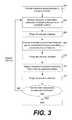
- FIG. 3is a process flow diagram depicting operations for a method in accordance with certain disclosed embodiments.
- FIGS. 4A-4Dare schematic illustrations of substrates during operations performed in accordance with certain disclosed embodiments.
- FIG. 5is a timing sequence diagram showing an example of cycles in a method in accordance with certain disclosed embodiments.
- FIG. 6is a schematic diagram of an example process chamber for performing certain disclosed embodiments.
- FIG. 7is a schematic diagram of an example process tool for performing certain disclosed embodiments.
- the implementations disclosed belowdescribe methods for depositing a material on a substrate such as a wafer, substrate, or other work piece.
- the work piecemay be of various shapes, sizes, and materials.
- other work pieces that may be used implementations disclosed hereininclude various articles such as printed circuit boards and the like.
- the processes and apparatusescan be used in the fabrication of semiconductor devices, displays, LEDs, photovoltaic panels and the like.
- ALDatomic layer deposition
- ALD processesuse surface-mediated deposition reactions to deposit films on a layer-by-layer basis in cycles.
- an ALD cyclemay include the following operations: (i) delivery/adsorption of a precursor, (ii) purging of precursor from the chamber, (iii) delivery of a second reactant and optionally ignite plasma, and (iv) purging of byproducts from the chamber.
- the reaction between the second reactant and the adsorbed precursor to form a film on the surface of a substrateaffects the film composition and properties, such as nonuniformity, stress, wet etch rate, dry etch rate, electrical properties (e.g., breakdown voltage and leakage current), etc.
- this reactioninvolves reacting oxygen plasma with carbon and nitrogen to form a gaseous species; oxidizing silicon to silicon oxide; eliminating trace carbon, nitrogen, and hydrogen impurities; and increasing bonding and densification of the film.
- ALD processesuse surface-mediated deposition reactions to deposit films on a layer-by-layer basis.
- a substrate surface that includes a population of surface active sitesis exposed to a gas phase distribution of a first precursor, such as a silicon-containing precursor, in a dose provided to a chamber housing the substrate.
- a first precursorsuch as a silicon-containing precursor
- Molecules of this first precursorare adsorbed onto the substrate surface, including chemisorbed species and/or physisorbed molecules of the first precursor.
- the adsorbed layermay include the compound as well as derivatives of the compound.
- an adsorbed layer of a silicon-containing precursormay include the silicon-containing precursor as well as derivatives of the silicon-containing precursor.
- the chamberis then evacuated to remove most or all of the first precursor remaining in gas phase so that mostly or only the adsorbed species remain.
- the chambermay not be fully evacuated.
- the reactormay be evacuated such that the partial pressure of the first precursor in gas phase is sufficiently low to mitigate a reaction.
- a second reactantsuch as an oxygen-containing reactant, is introduced to the chamber so that at least some of these molecules react with the first precursor adsorbed on the surface. In some processes, the second precursor reacts immediately with the adsorbed first precursor.
- the second reactantreacts only after a source of activation is applied temporally.
- the second reactantmay be ignited with the plasma.
- the chambermay then be evacuated again to remove unbound and/or unreacted second reactant molecules.
- the chambermay not be completely evacuated. Additional ALD cycles may be used to build film thickness.
- the ALD first precursor doseat least partially saturates the substrate surface.
- the dose phase of an ALD cycleconcludes before the precursor contacts the substrate to evenly saturate the surface.
- the precursor flowis turned off or diverted at this point, and only purge gas flows.
- the ALD processreduces the cycle time and increases throughput.
- precursor adsorptionis not saturation limited, the adsorbed precursor concentration may vary slightly across the substrate surface. Examples of ALD processes operating in the sub-saturation regime are provided in U.S.
- the ALD methodsinclude plasma activation.
- the ALD methods and apparatuses described hereinmay be conformal film deposition (CFD) methods, which are described generally in U.S. patent application Ser. No. 13/084,399 (now U.S. Pat. No. 8,728,956), filed Apr. 11, 2011, and titled “PLASMA ACTIVATED CONFORMAL FILM DEPOSITION,” and in U.S. patent application Ser. No. 13/084,305, filed Apr. 11, 2011, and titled “SILICON NITRIDE FILMS AND METHODS,” which are herein incorporated by reference in their entireties.
- CFDconformal film deposition
- ALD processesmay be used for blanket or patterned substrates.
- Substratesmay include “features” or “trenches.”
- Featuresmay be characterized by one or more of narrow and/or re-entrant openings, constrictions within the feature, and high aspect ratios.
- the featuremay be formed in one or more of the above described layers.
- One example of a featureis a hole or via in a semiconductor substrate or a layer on the substrate. Another example is a trench in a substrate or layer.
- the terms “trench” and “feature”may be used interchangeably in the present disclosure and will be understood to include any hole, via, or recessed region of a substrate.
- the featuremay have an under-layer, such as a barrier layer or adhesion layer.
- under-layersinclude dielectric layers and conducting layers, e.g., silicon oxides, silicon nitrides, silicon carbides, metal oxides, metal nitrides, metal carbides, and metal layers.
- Films deposited by ALDare typically conformal. Conformality of films may be measured by the step coverage. Step coverage may be calculated by comparing the average thickness of a deposited film on a bottom, sidewall, or top of a feature or trench to the average thickness of a deposited film on a bottom, sidewall, or top of a feature or trench. For example, step coverage may be calculated by dividing the average thickness of the deposited film on the sidewall by the average thickness of the deposited film at the top of the feature and multiplying it by 100 to obtain a percentage.
- ALDcan deposit highly conformal films, deposition of films into high aspect ratio features becomes challenging.
- the step coverage and uniformity of film property along the side walldepends on, among many factors, the transport of the deposition precursor, reactant ions and/or radicals, and by-products. As the dimension of the feature or trench is reduced, transport and diffusion of the deposition precursor and reactant becomes increasing difficult in the feature, thereby leading to formation of a seam and/or voids in high aspect ratio features.
- FIG. 1Ashows an example of a substrate 100 having feature or trench 101 which is filled with silicon oxide 102 by a conventional PEALD technique.
- FIG. 1Bshows an image of a substrate 110 after exposure to hydrofluoric acid (HF) used to etch the substrate 110 , which causes void 160 to be visible after the etching process.
- HFhydrofluoric acid
- the film deposited within the trenchmay have a different and more degraded film quality than the film deposited near the top of a trench. This may be because the second reactant species is unable to transport into the depths of the trench and the number and distribution of reactant species reaching the trench bottom is different from and less than at the top.
- the film qualitycan be evaluated by etching the deposited film in diluted HF and observing and comparing the amount of film etched at or near the top of the trenches and the amount of film etched along the sidewalls. Films having a high wet etch rate are more easily etched using HF.
- FIGS. 2A and 2BAn example is provided in FIGS. 2A and 2B .
- FIG. 2Ashows a substrate with a film deposited using exposures to cycles of a precursor and 2 -second exposures to a second reactant ignited with plasma at 495° C.
- FIG. 2Bshows a substrate with a film deposited using exposures to cycles of a precursor and 5-second exposures to a second reactant ignited with plasma at 495° C. As shown, the substrate in FIG. 2B has been sputtered at the trench edges 222 , resulting in a non-conformal film.
- Disclosed embodimentsmay be used to partially fill high aspect ratio structures, such as for forming contact liners, and may also be used to completely fill high aspect ratio structures, such as for gapfill applications.
- Disclosed embodimentsmay be suitable for depositing silicon-containing material into high aspect ratio features, such as silicon oxide, silicon, poly-silicon, and silicon nitride.Methods may be used for filling through so it can be us and for 3D NAND applications.
- Disclosed embodimentsreduce deposition at or near the top of features or trenches by removing adsorbed precursor from a precursor exposure dose at the top of the features while leaving most of the sidewalls and the bottom of the features saturated with adsorbed precursor prior to exposing the substrate to a second reactant and igniting a plasma to form a film conformal along most of the sidewalls and at the bottom of features while forming a partial or no film at the top of the features.
- exposures to an adsorbed precursor layer on a substrate to a post-dose treatmentmay be used in the initial ALD or PEALD cycles to allow bottom-up fill of features and trenches and prevent the opening at the top of the features and trenches from closing prior to filling the feature or trench.
- FIG. 3is a process flow diagram depicting operations for a method performed in accordance with certain disclosed embodiments. Although examples provided herein describe disclosed embodiments in the context of depositing silicon oxide films, it should be understood that disclosed embodiments may also be used to deposit films of any material.
- a substrateis provided to a process station or chamber of a single station or multi-station chamber. Suitable apparatuses for performing certain disclosed embodiments are further described below.
- the substrateis a semiconductor substrate.
- the substratemay be a silicon wafer, e.g., a 200-mm wafer, a 300-mm wafer, or a 450-mm wafer, such as wafers having one or more layers of material, such as dielectric, conducting, or semi-conducting material deposited thereon.
- Substratesmay have features such as via or contact holes, or trenches as previously described.
- a patterned substratemay have many features, each having different aspect ratios.
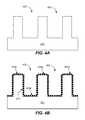
- FIG. 4Ashows an example substrate 401 including patterned trenches or features 403 .
- a featuremay have an aspect ratio of at least about 2:1, at least about 4:1, at least about 6:1, at least about 8:1, at least about 10:1, at least about 20:1, at least about 40:1 or higher.
- Some featuresmay have a depth of between about 1 ⁇ m and about 100 ⁇ m, or between about 4 ⁇ m and about 100 ⁇ m.
- the featuremay also have a dimension near the opening, e.g., an opening diameter or line width of less than about 5000 nm, or between about 25 nm and about 5000 nm, or between about 10 nm to 500 nm, or less than about 150 nm.
- Some featuresmay be through silicon vias having feature openings between 3 ⁇ m and 5 ⁇ m and feature depths between 50 ⁇ m and 100 ⁇ m, and may have a high aspect ratio, such as at least about 20:1.
- NAND structuresmay have feature openings of 150 to 500 nm and feature depths between 2 ⁇ m and 6 ⁇ m, and may have an aspect ratio of at least about 40:1.
- a via, trench or other recessed featuremay be referred to as an unfilled feature or a feature.
- the feature profilemay narrow gradually and/or include an overhang at the feature opening.
- a re-entrant profileis one that narrows from the bottom, closed end, or interior of the feature to the feature opening.
- a re-entrant profilemay be generated by asymmetric etching kinetics during patterning and/or the overhang due to non-conformal film step coverage in the previous film deposition, such as deposition of a diffusion barrier.
- the featuremay have a width smaller in the opening at the top of the feature than the width of the bottom of the feature.
- an inert gasmay be flowed.
- the inert gasis used as a carrier gas.
- Example carrier gasesinclude nitrogen, argon, helium, and neon.
- the carrier gasis used as a purge gas in some operations.
- the carrier gasis diverted.
- the inert gasmay be provided to assist with pressure and/or temperature control of the process chamber, evaporation of a liquid reactant, more rapid delivery of the reactant and/or as a sweep gas for removing process gases from the process chamber and/or process chamber plumbing.
- Disclosed embodimentsmay be performed at a chamber pressure between about 0.1 Torr and about 20 Torr.
- the methods disclosedmay be performed at a substrate temperature less than about 650° C., or less than about 450° C., or between about 50° C. and about 650° C., such as about 200° C.
- substrate temperature as described hereinrefers to the temperature at which a pedestal holding a substrate may be set.
- the pedestalmay be set to a temperature of less than about 450° C. to control the substrate temperature.
- the methodis performed at a higher temperature, such as greater than about 250° C., or greater than 450° C.
- FIG. 4Bshows an example substrate 401 including features 403 having been exposed to a deposition precursor (shown at 433 a and 433 b ), such that the deposition precursor molecules conformally adsorbs to the tops, sidewalls, and bottoms of the features.
- the deposition precursormay be a silicon-containing precursor in some embodiments.
- the substratemay be exposed to the deposition precursor for a duration sufficient to saturate the surface of a substrate having features, including the bottoms and sidewalls of features.
- the deposition precursormay fully saturate the surface of the substrate.
- a deposition precursoradsorbs onto the substrate surface in a self-limiting manner such that once active sites are occupied by the deposition precursor, little or no additional deposition precursor will be adsorbed on the substrate surface. For example, deposition precursors may be adsorbed onto about 60% of the substrate surface.
- the deposition precursorwhen the deposition precursor is flowed to the chamber, the deposition precursor adsorbs onto active sites on the surface of the substrate, forming a thin layer of the deposition precursor on the surface.
- this layermay be less than a monolayer, and may have a thickness between about 0.2 ⁇ and about 0.4 ⁇ .
- a silicon-containing precursoris a single reagent or mixture of reagents used to make a silicon-containing film, where the reagent or reagent mixture contains at least one silicon compound.
- the silicon-containing precursormay be, for example, a silane, a halosilane, or an aminosilane.
- a silicon-containing filmsuch as silicon oxide or silicon nitride, is deposited using disclosed embodiments, various suitable silicon-containing precursors may be used.
- Silicon-containing precursors suitable for use in accordance with disclosed embodimentsinclude polysilanes (H 3 Si—(SiH 2 ) n —SiH 3 ), where n ⁇ 0.
- silanesare silane (SiH 4 ), disilane (Si 2 H 6 ), and organosilanes such as methylsilane, ethylsilane, isopropylsilane, t-butylsilane, dimethylsilane, diethylsilane, di-t-butylsilane, allylsilane, sec-butylsilane, thexylsilane, isoamylsilane, t-butyldisilane, di-t-butyldisilane, and the like.
- a halosilaneincludes at least one halogen group and may or may not include hydrogens and/or carbon groups.
- halosilanesare iodosilanes, bromosilanes, chlorosilanes and fluorosilanes.
- halosilanes, particularly fluorosilanesmay form reactive halide species that can etch silicon materials when a plasma is struck, a halosilane may not be introduced to the chamber when a plasma is struck in some embodiments, so formation of a reactive halide species from a halosilane may be mitigated.
- chlorosilanesare tetrachlorosilane, trichlorosilane, dichlorosilane, monochlorosilane, chloroallylsilane, chloromethylsilane, dichloromethylsilane, chlorodimethylsilane, chloroethylsilane, t-butylchlorosilane, di-t-butylchlorosilane, chloroisopropylsilane, chloro- sec-butylsilane, t-butyldimethylchlorosilane, thexyldimethylchlorosilane, and the like.
- aminosilaneincludes at least one nitrogen atom bonded to a silicon atom, but may also contain hydrogens, oxygens, halogens, and carbons.
- Examples of aminosilanesare mono-, di-, tri- and tetra-aminosilane (H 3 Si(NH 2 ) 4 , H 2 Si(NH 2 ) 2 , HSi(NH 2 ) 3 , and Si(NH 2 ) 4 , respectively), as well as substituted mono-, di-, tri- and tetra-aminosilanes, for example, t-butylaminosilane, methylaminosilane, tert-butylsilanamine, bis(tertiarybutylamino)silane (SiH 2 (NHC(CH 3 ) 3 ) 2 ) (BTBAS), tert-butyl silylcarbamate, SiH(CH 3 )—(N(CH 3 ) 2 ) 2 , SiHCl—(N(CH 3
- the process chamberis optionally purged to remove excess deposition precursor in gas phase that did not adsorb onto the surface of the substrate.
- Purging the chambermay involve flowing one or more purge gases or sweep gases, which may be a carrier gas used in other operations such as described above, or may be a different gas.
- Example purge gasesinclude argon, nitrogen, hydrogen, and helium.
- purgingmay involve evacuating the chamber.
- operation 306may include one or more evacuation subphases for evacuating the process chamber. Alternatively, it will be appreciated that operation 306 may be omitted in some embodiments.
- Operation 306may have any suitable duration, such as between about 0 seconds and about 60 seconds, for example about 0.01 seconds.
- increasing a flow rate of a one or more purge gasesmay decrease the duration of operation 306 .
- a purge gas flow ratemay be adjusted according to various reactant thermodynamic characteristics and/or geometric characteristics of the process chamber and/or process chamber plumbing for modifying the duration of operation 306 .
- the duration of a purge phasemay be adjusted by modulating purge gas flow rate. This may reduce deposition cycle time, which may improve substrate throughput. After a purge, the deposition precursors remain adsorbed onto the substrate surface.
- the substrateis exposed to a post-dose treatment to preferentially remove adsorbed deposition precursor molecules from the top of the features.
- the “top” of a featureis defined as any region in the top 10% of the depth of the feature.
- Exposure to a post-dose treatment to preferentially remove adsorbed deposition precursor moleculesresults in a non-continuous, non-conformal adsorbed layer of precursor on the substrate such that after the substrate is exposed to a post-dose treatment, the bottom 90% of the depth of the feature (or bottom 80%, or bottom 70%, or bottom 60% of the depth of the feature) is at least about 90% saturated with adsorbed precursor, while little to no precursors are adsorbed at the top 10% of the features.
- the tops of the featureshave less than about 90% saturation, or less than about 70% saturation, or less than about 30% saturation, or less than about 10% saturation.
- the amount of saturation at the tops of the featurescan be modulated to changing process conditions of the post-dose treatment.
- the post-dose treatmentinvolves providing energy to the adsorbed layer at the top of the features to break chemical or mechanical bonds between the adsorbed precursor molecules and the underlying material (which may be semiconductor substrate material or a film deposited in prior cycles), or involves providing energy to the adsorbed layer at the top of the features to disintegrate adsorbed precursor molecules.
- the post-dose treatmentmay physically sputter the adsorbed layer of precursor molecules particularly at the tops of the features to remove the precursor molecules from being adsorbed to the substrate surface.
- a biasmay not be used.
- a biasmay be used to control the directionality of the plasma generated during the post-dose treatment.
- the biasmay be generated in either a powered showerhead or powered pedestal system.
- a post-dose treatmentmay remove hydroxyl bonds on the surface of the substrate, such as where disclosed embodiments are used for depositing silicon oxide into features. Without being bound by a particular theory, it is believed that removal of hydroxyl bonds will prevent adsorption of the precursor during a subsequent dosing operation (such as in operation 304 in a later, repeated cycle of deposition).
- an aminosilane precursormay bind to hydroxyl groups to adsorb onto the surface of the substrate, and a post-dose treatment may be used to remove hydroxyl bonds and prevent adsorption of the aminosilane precursor in subsequent precursor adsorption operations.
- the post-dose treatmentis performed at a substrate temperature between about 25° C. and about 650° C., or between about 25° C. and about 550° C.
- the substrate temperaturemay be modulated to prevent formation of a nitride where a nitrogen-containing gas is used in the post-dose treatment.
- nitrogenmay not react with an adsorbed layer of a silicon-containing precursor at about 400° C. so where nitrogen is used as a post-dose treatment, the temperature may be modulated such that the post-dose treatment is performed near 400° C., or less than 400° C. to prevent nitrogen from reacting with the silicon-containing precursor to form silicon nitride.
- the post-dose treatmentincludes exposure of the adsorbed precursor layer to an inert non-oxidizing plasma, to ultraviolet (UV) radiation, or both. Exposure to a non-oxidizing plasma may be facilitated by generating a plasma in a remote plasma generator or generating a plasma in the processing chamber where the substrate is being processed. A non-oxidizing gas is flowed to a plasma generating region, which may be the remote plasma generator or the processing chamber, and a plasma is ignited.
- Process conditionsincluding the plasma power, plasma frequency, exposure time to a non-oxidizing plasma, flow rate of the non-oxidizing gas, chamber pressure, and pedestal temperature may be modulated to prevent formation of silicon nitride if nitrogen or ammonia is used as a non-oxidizing gas for post-dose treatments in processes used to deposit silicon oxide.
- silicon nitridemay form on the surface of the substrate during a post-dose treatment, but due to the bond energies of silicon to oxygen and silicon to nitrogen, where silicon oxide is formed in subsequent operations, silicon nitride can be converted to oxide.
- Process conditionsare modulated to avoid formation of conversion plasmas, such as an oxygen plasma for forming oxide, ammonia plasma for forming nitride, and carbon-containing plasma for forming carbide.
- an intermediate compoundmay form during post-dose treatment.
- an intermediate compoundmay include silicon atoms bound to nitrogen atoms from a nitrogen or ammonia post-dose treatment. Even if an intermediate compound is formed, plasma is generated at low energy such that the intermediate species converts to the desired film to be deposited when exposed to the plasma.
- oxygen plasmamay be used after a post-dose treatment such that even if an intermediate compound is formed after post-dose treatment, the oxygen plasma will convert the intermediate compound into silicon oxide.
- the plasma in operation 308may be generated at a power at less than about 6 kW, or between about 500 W and about 4000 W.
- the post-dose treatment when using a gas or plasmamay be performed for a duration between about 0.1 seconds and about 10 seconds, or between about 0.3 seconds and about 3 seconds.
- the non-oxidizing gas or post-dose treatment gasmay be used without generating a plasma.
- a post-dose treatment performed using ultraviolet radiationmay be performed by exposing the substrate to UV light having a wavelength between about 10 nm and about 400 nm.
- the substratemay be exposed to ultraviolet radiation for a duration between about 0.1 seconds and about 10 seconds. The duration and wavelength of UV light used depends on the precursor used and the aspect ratio of the features on the substrate.
- FIG. 4Cshows an example substrate 401 having features 403 where some of the adsorbed precursor molecules at the top of the features 403 are removed, while the adsorbed precursor on the bottoms and sidewalls 413 of the features 403 remain adsorbed to the substrate.
- the process chamberis optionally purged to remove the removed adsorbed precursor molecules from the post-dose treatment process. Purging may involve any of the processes and process conditions described above with respect to operation 306 .
- the substrateis exposed to a reactant and a plasma is ignited such that the adsorbed silicon-containing precursor layer remaining on the surface of the substrate is converted to the desired film, such as silicon oxide.
- a plasmais ignited such that the adsorbed silicon-containing precursor layer remaining on the surface of the substrate is converted to the desired film, such as silicon oxide.
- the term “reactant” or “second reactant”may be used to describe one or more gases introduced to the chamber when plasma is ignited in a deposition cycle.
- the second reactantis an oxygen-containing reactant or oxidant, to form at least a partial silicon oxide film on the surface of the substrate.
- This operationmay be performed for a duration between about 0.05 seconds and about 10 seconds. The duration of this operation may be modulated depending on the depth of the trench or feature where material is being deposited, and depending on the number of cycles used as further described below with respect to operation 316 .
- plasma energyis provided to activate the second reactant, such as an oxygen-containing gas, into ions, radicals, neutral species, and other activated species, which react with the remaining adsorbed layer of the silicon-containing deposition precursor.
- the plasmamay directly or indirectly activate the oxygen-containing gas phase molecules to form oxygen radicals or ions.
- Conditions of the chambermay be monitored such that sufficient plasma species can diffuse into trenches and tailor the feature profile and improve conformality within features and trenches.
- the plasmais an in-situ plasma, such that the plasma is formed directly above the substrate surface in the chamber.
- the in-situ plasmamay be ignited at a power per substrate area between about 0.2122 W/cm 2 and about 2.122 W/cm 2 .
- the powermay range from about 150 W to about 6000 W, or from about 600 W to about 6000 W, or from about 800 W to about 4000 W, for a chamber processing four 300 mm wafers.
- plasmas for ALD processesmay be generated by applying a radio frequency (RF) field to a gas using two capacitively coupled plates. Ionization of the gas between plates by the RF field ignites the plasma, creating free electrons in the plasma discharge region.
- RFradio frequency
- the RF fieldmay be coupled via any suitable electrodes.
- a high frequency plasmais used having a frequency of at least about 13.56 MHz, or at least about 27 MHz, or at least about 40 MHz, or at least about 60 MHz.
- a microwave-based plasmamay be used.
- electrodesinclude process gas distribution showerheads and substrate support pedestals.
- plasmas for ALD processesmay be formed by one or more suitable methods other than capacitive coupling of an RF field to a gas.
- the plasmais a remote plasma, such that a second reactant is ignited in a remote plasma generator upstream of the chamber, then delivered to the chamber where the substrate is housed.
- Example oxygen-containing reactants or oxidantsinclude a mixture of oxygen and a weak oxidizer such as nitrous oxide, carbon monoxide, carbon dioxide, nitric oxide, nitrogen dioxide, sulfur oxide, sulfur dioxide, oxygen-containing hydrocarbons (e.g., C x H y O z ) and/or water.
- a weak oxidizersuch as nitrous oxide, carbon monoxide, carbon dioxide, nitric oxide, nitrogen dioxide, sulfur oxide, sulfur dioxide, oxygen-containing hydrocarbons (e.g., C x H y O z ) and/or water.
- the oxidation reactantmay be entirely weak oxidizer.
- the oxidation reactantmay include ozone.
- the second reactantmay be a carbon-containing reactant.
- a nitrogen-containing reactantmay be used for deposition of silicon nitride.
- a nitrogen-containing reactantis a reactant or mixture of reactants that includes at least one nitrogen, for example, ammonia, hydrazine, amines (amines bearing carbon) such as methylamine, dimethylamine, ethylamine, isopropylamine, t-butylamine, di-t-butylamine, cyclopropylamine, sec-butylamine, cyclobutylamine, isoamylamine, 2-methylbutan-2-amine, trimethylamine, diisopropylamine, diethylisopropylamine, di-t-butylhydrazine, as well as aromatic containing amines such as anilines, pyridines, and benzylamines.
- aminesamines bearing carbon
- Aminesmay be primary, secondary, tertiary, or quaternary (for example, tetraalkylammonium compounds).
- a nitrogen-containing reactantcan contain heteroatoms other than nitrogen, for example, hydroxylamine, t-butyloxycarbonyl amine, and N-t-butyl hydroxylamine are nitrogen-containing reactants.
- Example nitrogen-containing reactantsinclude nitrogen gas, ammonia, and amines.
- a dopantmay also be added as a second reactant.
- FIG. 4Dshows an example substrate 401 with trenches or features 403 whereby the substrate has been exposed a second reactant with a plasma and the adsorbed layer of precursor molecules has been reacted and converted to form a film 450 on the substrate, where the film 450 is preferentially deposited along the sidewalls and the bottom of the trenches, while little to no deposition of the film is formed over the top 424 of the features 403 .
- the thickness of the deposited silicon-containing filmis less than the thickness of the deposited silicon-containing film at the bottoms of the features.
- the process chamberis optionally purged to remove any residual byproducts. Purging may involve any of the processes and process conditions described above with respect to operation 306 .
- operation 316 of FIG. 3it is determined whether the desired thickness of film has been deposited. If not, operations 304 - 314 are repeated in sufficient cycles to deposit a desired thickness of film. Any suitable number of deposition cycles may be included in a process to deposit a desired film thickness of the desired film in accordance with certain disclosed embodiments. In various embodiments, operations may be repeated for n cycles, where n is an integer greater than or equal to 2 . For example, in some embodiments, operations 304 - 314 may be repeated for two or more cycles.
- the frequency of performing the post-dose treatment of operation 308 to preferentially remove adsorbed precursor at the top of the featuresmay depend on the size of the features and the amount of film to be deposited in the features. As noted above, exposure to a post-dose treatment may not necessarily be performed in every cycle. In later, repeated cycles, as the trench depth decreases (e.g., as the trench is filled with material such as silicon oxide), the frequency of performing a post-dose treatment may be modified or reduced. For example, as the trench fills with silicon oxide, the aspect ratio of the remaining feature to be filled with silicon oxide decreases and the post-dose treatment may not need to be performed to avoid formation of a void.
- the duration of operation 312may depend on the size of the feature or trench to be filled and may be reduced in later repeated deposition cycles.
- the initial cycles of performing disclosed embodimentsmay use a longer duration of operation 312 (such as between about 0.1 seconds and about 10 seconds) to allow diffusion of the second reactant plasma into trenches and features to reach with adsorbed precursor at the bottom and sidewalls of trenches and features.
- the duration of operation 312may be gradually reduced as the distance the second reactant plasma travels to diffuse to the adsorbed layer of precursor molecules decreases.
- the post-dose treatment operationmay not be performed in every cycle, or in any cycle.
- FIG. 5is a timing sequence diagram of example pulses in accordance with certain disclosed embodiments.
- FIG. 5shows phases in an example ALD process 500 for various process parameters, such as carrier gas flow, first precursor flow, post-dose treatment gas flow, plasma, and second reactant flow.
- the linesindicate when the flow or plasma is turned on and off, accordingly.
- Additional example process parametersinclude, but are not limited to, flow rates for inert and reactant species, plasma power and frequency, substrate temperature, and process chamber pressure.
- the example provided in FIG. 5depicts two deposition cycles 590 A and 590 B for depositing a silicon oxide film using a silicon-containing precursor and oxygen plasma, and a non-oxidizing plasma is used for post-dose treatment.
- deposition cycle 590 Aincludes a silicon precursor exposure phase 504 A, which may correspond to operation 304 of FIG. 3 ; a purge phase 506 A (which may be optional and may correspond to operation 306 of FIG. 3 ); a post-dose treatment phase 508 A, which may correspond to operation 308 of FIG. 3 ; a purge phase 510 A (which may be optional and may correspond to operation 310 of FIG. 3 ); an oxygen plasma exposure phase 512 A, which may correspond to combining operation 312 in FIG. 3 ; and purge phase 514 A which may correspond to operation 314 of FIG. 3 .
- a carrier gasis flowed throughout the process. It will be understood that any suitable carrier gas may be used as describe elsewhere herein.
- the carrier gasis used as a purge gas.
- the carrier gasis depicted as being both a carrier gas and a purge gas during pure phases 506 A, 510 A, 514 A, 506 B, 510 B, and 514 B.
- the carrier gasmay be different than the purge gas.
- a carrier gasis only flowed during one or more of the purge phases ( 506 A, 510 A, 514 A, 506 B, 510 B, and 514 B).
- a carrier gasmay be any of those described above with respect to operation 306 of FIG. 3 .
- silicon precursor exposure phase 504 Awhich may correspond to operation 304 of FIG. 3
- a silicon-containing precursoris flowed with a carrier gas and oxygen flow is turned off.
- the plasmais also turned off, and non-oxidizing gas flow is also turned off.
- purge phase 506 Aall gas flows except the carrier gas are turned off and the plasma is turned off. This may correspond to operation 306 of FIG. 3 .
- post-dose treatment phase 508 Athe carrier gas remains on, the non-oxidizing gas flow is turned on, and the plasma is turned on to generate a non-oxidizing plasma to preferentially remove adsorbed silicon-containing precursor molecules at or near the top of features.
- the silicon-containing precursor and oxygen gas flowsare turned off. This may correspond to operation 308 of FIG. 3 .
- purge phase 510 Aall gas flows except the carrier gas are turned off and the plasma is turned off. This may correspond to operation 310 of FIG. 3 .
- oxygen plasma exposure phase 512 Athe carrier gas is flowed with the oxygen flow, while the plasma is turned on to ignite and generate and oxygen-containing plasma. This oxygen-containing plasma reacts with the remaining adsorbed precursor to selectively form silicon oxide along sidewalls and the bottom of trenches while forming little to no silicon oxide at or near the tops of the trenches. This operation may correspond to combining operations 312 of FIG. 3 .
- purge phase 514 Athe carrier gas flow remains on and all other gas flows and plasma is turned off.
- deposition cycle 590 Bincludes silicon-containing exposure phase 504 , purge phase 506 B (which may be optional), post-dose treatment phase 508 B, purge phase 510 B (which may be optional), oxygen plasma exposure phase 512 B, and purge phase 514 B (which may be optional).
- FIG. 6depicts a schematic illustration of an embodiment of an atomic layer deposition (ALD) process station 600 having a process chamber 602 for maintaining a low-pressure environment.
- a plurality of ALD process stationsmay be included in a common low pressure process tool environment.
- FIG. 7depicts an embodiment of a multi-station processing tool 700 .
- one or more hardware parameters of ALD process station 600may be adjusted programmatically by one or more computer controllers 650 .
- ALD process station 600fluidly communicates with reactant delivery system 601 a for delivering process gases to a distribution showerhead 606 .
- Reactant delivery system 601 aincludes a mixing vessel 604 for blending and/or conditioning process gases, such as a silicon-containing gas, or oxygen-containing gas, or post-dose treatment gases such as non-oxidizing gases, for delivery to showerhead 606 .
- One or more mixing vessel inlet valves 620may control introduction of process gases to mixing vessel 604 .
- the post-dose treatmentis performed in process station 600 and the film deposition is also performed in the same process station 600 .
- the ALD process station 600may be used to deliver a deposition precursor gas to the process chamber 602 , then deliver a non-oxidizing gas and ignite a plasma to preferentially remove adsorbed precursor on a substrate, then deliver a second reactant and ignite a plasma to convert remaining adsorbed precursors on the substrate to a film such as silicon oxide.
- the post-dose treatmentis performed in a process station separate from the ALD process station 600 , such as in another station of the multi-station processing tool 700 as further described below with respect to FIG. 7 .
- the embodiment of FIG. 6includes a vaporization point 603 for vaporizing liquid reactant to be supplied to the mixing vessel 604 .
- vaporization point 603may be a heated vaporizer.
- the saturated reactant vapor produced from such vaporizersmay condense in downstream delivery piping. Exposure of incompatible gases to the condensed reactant may create small particles. These small particles may clog piping, impede valve operation, contaminate substrates, etc.
- Some approaches to addressing these issuesinvolve purging and/or evacuating the delivery piping to remove residual reactant. However, purging the delivery piping may increase process station cycle time, degrading process station throughput.
- delivery piping downstream of vaporization point 603may be heat traced.
- mixing vessel 604may also be heat traced.
- piping downstream of vaporization point 603has an increasing temperature profile extending from approximately 100° C. to approximately 150° C. at mixing vessel 604 .
- a liquid precursor or liquid reactantmay be vaporized at a liquid injector (not shown).
- a liquid injectormay inject pulses of a liquid reactant into a carrier gas stream upstream of the mixing vessel 604 .
- a liquid injectormay vaporize the reactant by flashing the liquid from a higher pressure to a lower pressure.
- a liquid injectormay atomize the liquid into dispersed microdroplets that are subsequently vaporized in a heated delivery pipe. Smaller droplets may vaporize faster than larger droplets, reducing a delay between liquid injection and complete vaporization. Faster vaporization may reduce a length of piping downstream from vaporization point 603 .
- a liquid injectormay be mounted directly to mixing vessel 604 .
- a liquid injectormay be mounted directly to showerhead 606 .
- a liquid flow controller (LFC) upstream of vaporization point 603may be provided for controlling a mass flow of liquid for vaporization and delivery to process chamber 602 .
- the LFCmay include a thermal mass flow meter (MFM) located downstream of the LFC.
- a plunger valve of the LFCmay then be adjusted responsive to feedback control signals provided by a proportional-integral-derivative (PID) controller in electrical communication with the MFM.
- PIDproportional-integral-derivative
- the LFCmay be dynamically switched between a feedback control mode and a direct control mode. In some embodiments, this may be performed by disabling a sense tube of the LFC and the PID controller.
- showerhead 606distributes process gases toward substrate 612 .
- the substrate 612is located beneath showerhead 606 and is shown resting on a pedestal 608 .
- showerhead 606may have any suitable shape, and may have any suitable number and arrangement of ports for distributing process gases to substrate 612 .
- pedestal 608may be raised or lowered to expose substrate 612 to a volume between the substrate 612 and the showerhead 606 .
- pedestal 608may be temperature controlled via heater 610 .
- Pedestal 608may be set to any suitable temperature, such as between about 25° C. and about 650° C. during operations for performing various disclosed embodiments. It will be appreciated that, in some embodiments, pedestal height may be adjusted programmatically by a suitable computer controller 650 .
- adjusting a height of pedestal 608may allow a plasma density to be varied during plasma activation cycles and post-dose treatment operations performed in certain disclosed embodiments.
- pedestal 608may be lowered during another substrate transfer phase to allow removal of substrate 612 from pedestal 608 .
- a position of showerhead 606may be adjusted relative to pedestal 608 to vary a volume between the substrate 612 and the showerhead 606 . Further, it will be appreciated that a vertical position of pedestal 608 and/or showerhead 606 may be varied by any suitable mechanism within the scope of the present disclosure. In some embodiments, pedestal 608 may include a rotational axis for rotating an orientation of substrate 612 . It will be appreciated that, in some embodiments, one or more of these example adjustments may be performed programmatically by one or more suitable computer controllers 650 . The computer controller 650 may include any of the features described below with respect to controller 750 of FIG. 7 .
- showerhead 606 and pedestal 608electrically communicate with a radio frequency (RF) power supply 614 and matching network 616 for powering a plasma.
- the plasma energymay be controlled by controlling one or more of a process station pressure, a gas concentration, an RF source power, an RF source frequency, and a plasma power pulse timing.
- RF power supply 614 and matching network 616may be operated at any suitable power to form a plasma having a desired composition of radical species. Examples of suitable powers are included above.
- RF power supply 614may provide RF power of any suitable frequency.
- RF power supply 614may be configured to control high- and low-frequency RF power sources independently of one another.
- Example low-frequency RF frequenciesmay include, but are not limited to, frequencies between 0 kHz and 500 kHz.
- Example high-frequency RF frequenciesmay include, but are not limited to, frequencies between 1.8 MHz and 2.45 GHz, or greater than about 13.56 MHz, or greater than 27MHz, or greater than 40 MHz, or greater than 60 MHz. It will be appreciated that any suitable parameters may be modulated discretely or continuously to provide plasma energy for the surface reactions.
- the plasma conditionsmay be controlled and/or maintained such that plasma generated for a post-dose treatment operation preferentially removes adsorbed precursor molecules at or near feature openings rather than in sidewalls or at the bottom of features.
- the plasma powermay be intermittently pulsed to reduce ion bombardment with the substrate surface relative to continuously powered plasmas.
- the plasmamay be monitored in-situ by one or more plasma monitors.
- plasma powermay be monitored by one or more voltage, current sensors (e.g., VI probes).
- plasma density and/or process gas concentrationmay be measured by one or more optical emission spectroscopy sensors (OES).
- OESoptical emission spectroscopy sensors
- one or more plasma parametersmay be programmatically adjusted based on measurements from such in-situ plasma monitors.
- an OES sensormay be used in a feedback loop for providing programmatic control of plasma power.
- other monitorsmay be used to monitor the plasma and other process characteristics. Such monitors may include, but are not limited to, infrared (IR) monitors, acoustic monitors, and pressure transducers.
- instructions for a controller 650may be provided via input/output control (IOC) sequencing instructions.
- the instructions for setting conditions for a process phasemay be included in a corresponding recipe phase of a process recipe.
- process recipe phasesmay be sequentially arranged, so that all instructions for a process phase are executed concurrently with that process phase.
- instructions for setting one or more reactor parametersmay be included in a recipe phase.
- a first recipe phasemay include instructions for setting a flow rate of an inert and/or a reactant gas (e.g., the first precursor such as a silicon-containing precursor), instructions for setting a flow rate of a carrier gas (such as argon), and time delay instructions for the first recipe phase.
- a second, subsequent recipe phasemay include instructions for modulating or stopping a flow rate of an inert and/or a reactant gas, and instructions for modulating a flow rate of a carrier or purge gas and time delay instructions for the second recipe phase.
- a third recipe phasemay include instructions for modulating a flow rate of a post-dose treatment gas such as nitrogen when the process is programmed to deposit silicon oxide, instructions for modulating the flow rate of a carrier or purge gas, instructions for igniting a plasma, and time delay instructions for the third recipe phase.
- a fourth, subsequent recipe phasemay include instructions for modulating or stopping a flow rate of an inert and/or a post-dose treatment gas, and instructions for modulating a flow rate of a carrier or purge gas and time delay instructions for the fourth recipe phase.
- a fifth recipe phasemay include instructions for modulating a flow rate of a second reactant gas such as oxygen, instructions for modulating the flow rate of a carrier or purge gas, instructions for igniting a plasma, and time delay instructions for the fifth recipe phase.
- a sixth, subsequent recipe phasemay include instructions for modulating or stopping a flow rate of an inert and/or a reactant gas, and instructions for modulating a flow rate of a carrier or purge gas and time delay instructions for the sixth recipe phase. It will be appreciated that these recipe phases may be further subdivided and/or iterated in any suitable way within the scope of the present disclosure.
- pressure control for process station 600may be provided by butterfly valve 618 . As shown in the embodiment of FIG. 6 , butterfly valve 618 throttles a vacuum provided by a downstream vacuum pump (not shown). However, in some embodiments, pressure control of process station 600 may also be adjusted by varying a flow rate of one or more gases introduced to the process station 600 .
- FIG. 7shows a schematic view of an embodiment of a multi-station processing tool 700 with an inbound load lock 702 and an outbound load lock 704 , either or both of which may include a remote plasma source (not shown).
- a robot 706at atmospheric pressure, is configured to move wafers from a cassette loaded through a pod 708 into inbound load lock 702 via an atmospheric port 710 .
- a wafer(not shown) is placed by the robot 706 on a pedestal 712 in the inbound load lock 702 , the atmospheric port 710 is closed, and the load lock inbound 702 is pumped down.
- the wafermay be exposed to a remote plasma treatment in the inbound load lock 702 prior to being introduced into a processing chamber 714 . Further, the wafer also may be heated in the inbound load lock 702 as well, for example, to remove moisture and adsorbed gases. Next, a chamber transport port 716 to processing chamber 714 is opened, and another robot (not shown) places the wafer into the reactor on a pedestal of a first station shown in the reactor for processing. While the embodiment depicted in FIG. 7 includes load locks, it will be appreciated that, in some embodiments, direct entry of a wafer into a process station may be provided.
- the depicted processing chamber 714includes four process stations, numbered from 1 to 4 in the embodiment shown in FIG. 7 .
- Each stationhas a heated pedestal (shown at 718 for station 1), and gas line inlets.
- each process stationmay have different or multiple purposes.
- a process stationmay be switchable between an ALD and plasma-enhanced ALD process mode.
- post-dose treatment operationsmay be performed in one station, while exposure to a deposition precursor and exposure to a second reactant and plasma may be performed in another station.
- exposure to a deposition precursor, post-dose treatment, and exposure to a second reactant and plasmaare performed in the same station.
- processing chamber 714may include one or more matched pairs of ALD and plasma-enhanced ALD process stations. While the depicted processing chamber 714 includes four stations, it will be understood that a processing chamber according to the present disclosure may have any suitable number of stations. For example, in some embodiments, a processing chamber may have five or more stations, while in other embodiments a processing chamber may have three or fewer stations.
- FIG. 7depicts an embodiment of a wafer handling system 790 for transferring wafers within processing chamber 714 .
- wafer handling system 790may transfer wafers between various process stations and/or between a process station and a load lock. It will be appreciated that any suitable wafer handling system may be employed. Non-limiting examples include wafer carousels and wafer handling robots.
- FIG. 7also depicts an embodiment of a system controller 750 employed to control process conditions and hardware states of process tool 700 .
- System controller 750may include one or more memory devices 756 , one or more mass storage devices 754 , and one or more processors 752 .
- Processor 752may include a CPU or computer, analog, and/or digital input/output connections, stepper motor controller boards, etc.
- system controller 750controls all of the activities of process tool 700 .
- System controller 750executes system control software 758 stored in mass storage device 754 , loaded into memory device 756 , and executed on processor 752 .
- the control logicmay be hard coded in the controller 750 .
- Applications Specific Integrated Circuits, Programmable Logic Devicese.g., field-programmable gate arrays, or FPGAs
- FPGAsfield-programmable gate arrays
- System control software 758may include instructions for controlling the timing, mixture of gases, gas flow rates, chamber and/or station pressure, chamber and/or station temperature, wafer temperature, target power levels, RF power levels, substrate pedestal, chuck and/or susceptor position, and other parameters of a particular process performed by process tool 700 .
- System control software 758may be configured in any suitable way. For example, various process tool component subroutines or control objects may be written to control operation of the process tool components used to carry out various process tool processes.
- System control software 758may be coded in any suitable computer readable programming language.
- system control software 758may include input/output control (IOC) sequencing instructions for controlling the various parameters described above.
- IOCinput/output control
- Other computer software and/or programs stored on mass storage device 754 and/or memory device 756 associated with system controller 750may be employed in some embodiments. Examples of programs or sections of programs for this purpose include a substrate positioning program, a process gas control program, a pressure control program, a heater control program, and a plasma control program.
- a substrate positioning programmay include program code for process tool components that are used to load the substrate onto pedestal 718 and to control the spacing between the substrate and other parts of process tool 700 .
- a process gas control programmay include code for controlling gas composition (e.g., silicon-containing gases, oxygen-containing gases, gases for performing a post-dose treatment, and purge gases as described herein) and flow rates and optionally for flowing gas into one or more process stations prior to deposition in order to stabilize the pressure in the process station.
- a pressure control programmay include code for controlling the pressure in the process station by regulating, for example, a throttle valve in the exhaust system of the process station, a gas flow into the process station, etc.
- a heater control programmay include code for controlling the current to a heating unit that is used to heat the substrate.
- the heater control programmay control delivery of a heat transfer gas (such as helium) to the substrate.
- a plasma control programmay include code for setting RF power levels applied to the process electrodes in one or more process stations in accordance with the embodiments herein.
- a pressure control programmay include code for maintaining the pressure in the reaction chamber in accordance with the embodiments herein.
- the user interfacemay include a display screen, graphical software displays of the apparatus and/or process conditions, and user input devices such as pointing devices, keyboards, touch screens, microphones, etc.
- parameters adjusted by system controller 750may relate to process conditions.
- process conditionsinclude process gas composition and flow rates, temperature, pressure, plasma conditions (such as RF bias power levels), pressure, temperature, etc. These parameters may be provided to the user in the form of a recipe, which may be entered utilizing the user interface.
- Signals for monitoring the processmay be provided by analog and/or digital input connections of system controller 750 from various process tool sensors.
- the signals for controlling the processmay be output on the analog and digital output connections of process tool 700 .
- process tool sensorsthat may be monitored include mass flow controllers, pressure sensors (such as manometers), thermocouples, etc. Appropriately programmed feedback and control algorithms may be used with data from these sensors to maintain process conditions.
- System controller 750may provide program instructions for implementing the above-described deposition processes.
- the program instructionsmay control a variety of process parameters, such as DC power level, RF bias power level, pressure, temperature, etc.
- the instructionsmay control the parameters to operate in-situ deposition of film stacks according to various embodiments described herein.
- the system controller 750will typically include one or more memory devices and one or more processors configured to execute the instructions so that the apparatus will perform a method in accordance with disclosed embodiments.
- Machine-readable media containing instructions for controlling process operations in accordance with disclosed embodimentsmay be coupled to the system controller 750 .
- the system controller 750is part of a system, which may be part of the above-described examples.
- Such systemscan include semiconductor processing equipment, including a processing tool or tools, chamber or chambers, a platform or platforms for processing, and/or specific processing components (a wafer pedestal, a gas flow system, etc.).
- These systemsmay be integrated with electronics for controlling their operation before, during, and after processing of a semiconductor wafer or substrate.
- the electronicsmay be referred to as the “controller,” which may control various components or subparts of the system or systems.
- the system controller 750may be programmed to control any of the processes disclosed herein, including the delivery of processing gases, temperature settings (e.g., heating and/or cooling), pressure settings, vacuum settings, power settings, radio frequency (RF) generator settings, RF matching circuit settings, frequency settings, flow rate settings, fluid delivery settings, positional and operation settings, wafer transfers into and out of a tool and other transfer tools and/or load locks connected to or interfaced with a specific system.
- temperature settingse.g., heating and/or cooling
- pressure settingse.g., vacuum settings, power settings, radio frequency (RF) generator settings, RF matching circuit settings, frequency settings, flow rate settings, fluid delivery settings, positional and operation settings
- RFradio frequency
- the system controller 750may be defined as electronics having various integrated circuits, logic, memory, and/or software that receive instructions, issue instructions, control operation, enable cleaning operations, enable endpoint measurements, and the like.
- the integrated circuitsmay include chips in the form of firmware that store program instructions, digital signal processors (DSPs), chips defined as application specific integrated circuits (ASICs), and/or one or more microprocessors, or microcontrollers that execute program instructions (e.g., software).
- Program instructionsmay be instructions communicated to the system controller 750 in the form of various individual settings (or program files), defining operational parameters for carrying out a particular process on or for a semiconductor wafer or to a system.
- the operational parametersmay, in some embodiments, be part of a recipe defined by process engineers to accomplish one or more processing steps during the fabrication of one or more layers, materials, metals, oxides, silicon, silicon dioxide, surfaces, circuits, and/or dies of a wafer.
- the system controller 750may be a part of or coupled to a computer that is integrated with, coupled to the system, otherwise networked to the system, or a combination thereof.
- the system controller 750may be in the “cloud” or all or a part of a fab host computer system, which can allow for remote access of the wafer processing.
- the computermay enable remote access to the system to monitor current progress of fabrication operations, examine a history of past fabrication operations, examine trends or performance metrics from a plurality of fabrication operations, to change parameters of current processing, to set processing steps to follow a current processing, or to start a new process.
- a remote computere.g.
- a servercan provide process recipes to a system over a network, which may include a local network or the Internet.
- the remote computermay include a user interface that enables entry or programming of parameters and/or settings, which are then communicated to the system from the remote computer.
- the system controller 750receives instructions in the form of data, which specify parameters for each of the processing steps to be performed during one or more operations. It should be understood that the parameters may be specific to the type of process to be performed and the type of tool that the system controller 750 is configured to interface with or control.
- the system controller 750may be distributed, such as by including one or more discrete controllers that are networked together and working towards a common purpose, such as the processes and controls described herein.
- An example of a distributed controller for such purposeswould be one or more integrated circuits on a chamber in communication with one or more integrated circuits located remotely (such as at the platform level or as part of a remote computer) that combine to control a process on the chamber.
- example systemsmay include a plasma etch chamber or module, a deposition chamber or module, a spin-rinse chamber or module, a metal plating chamber or module, a clean chamber or module, a bevel edge etch chamber or module, a physical vapor deposition (PVD) chamber or module, a chemical vapor deposition (CVD) chamber or module, an ALD chamber or module, an atomic layer etch (ALE) chamber or module, an ion implantation chamber or module, a track chamber or module, and any other semiconductor processing systems that may be associated or used in the fabrication and/or manufacturing of semiconductor wafers.
- PVDphysical vapor deposition
- CVDchemical vapor deposition
- ALDatomic layer etch
- ALEatomic layer etch
- the system controller 750might communicate with one or more of other tool circuits or modules, other tool components, cluster tools, other tool interfaces, adjacent tools, neighboring tools, tools located throughout a factory, a main computer, another controller, or tools used in material transport that bring containers of wafers to and from tool locations and/or load ports in a semiconductor manufacturing factory.
- the apparatus/process described hereinmay be used in conjunction with lithographic patterning tools or processes, for example, for the fabrication or manufacture of semiconductor devices, displays, LEDs, photovoltaic panels and the like. Typically, though not necessarily, such tools/processes will be used or conducted together in a common fabrication facility.
- Lithographic patterning of a filmtypically includes some or all of the following operations, each operation enabled with a number of possible tools: (1) application of photoresist on a workpiece, i.e., substrate, using a spin-on or spray-on tool; (2) curing of photoresist using a hot plate or furnace or UV curing tool; (3) exposing the photoresist to visible or UV or x-ray light with a tool such as a wafer stepper; (4) developing the resist so as to selectively remove resist and thereby pattern it using a tool such as a wet bench; (5) transferring the resist pattern into an underlying film or workpiece by using a dry or plasma-assisted etching tool; and (6) removing the resist using a tool such as an RF or microwave plasma resist stripper.
- a toolsuch as an RF or microwave plasma resist stripper.
- a silicon oxide filmwas deposited on a substrate exposed to cycles of the following operations: exposure to a silicon-containing precursor, purging using argon, exposure to nitrogen plasma as a non-oxidizing plasma used for post-dose treatment, purging using argon, exposure to oxygen plasma, and purging using argon.
- the depositionwas performed at a pedestal temperature of 50° C.
- the nitrogen plasma post-dose treatmentwas performed at varying plasma powers as shown in Table 1 below and with various exposure times, where the exposure time is the duration of exposure to a single post-dose treatment in one cycle of PEALD.
- the oxygen plasma used to convert the silicon-containing precursor adsorbed onto the substrate to silicon oxidewas generated at a power of 500 W, with each exposure to oxygen plasma lasting 0.3 seconds within each cycle.
- the deposition rate of silicon oxide per cyclewas evaluated and is shown in Table 1.
- a silicon oxide filmwas deposited on a substrate exposed to cycles of the following operations: exposure to a silicon-containing precursor, purging using argon, exposure to nitrogen plasma as a non-oxidizing plasma used for post-dose treatment, purging using argon, exposure to oxygen plasma, and purging using argon.
- a second silicon oxide film was deposited on a substratewas exposed to cycles of the following operations: exposure to a silicon-containing precursor, purging using argon, exposure to argon plasma as a non-oxidizing plasma used for post-dose treatment, purging using argon, exposure to oxygen plasma, and purging using argon.
- the depositionswere performed at a pedestal temperature of 400° C.
- the plasma post-dose treatmentswere performed at varying plasma powers as shown in Table 2 below and with various exposure times, where the exposure time is the duration of exposure to a single post-dose treatment in one cycle of PEALD.
- the oxygen plasma used to convert the silicon-containing precursor adsorbed onto the substrate to silicon oxidewas generated at a power of 4000 W, with each exposure to oxygen plasma lasting 0.25 seconds within each cycle.
- Experiment 2Like Experiment 1, a reduction in deposition rate was observed as plasma power and time increased, suggesting that silicon was removed after adsorption and/or some densification of the deposited film was occurring in both processes. As compared to Experiment 1, which was conducted at a lower temperature, the deposition rates in Experiment 2 were less than that of Experiment 1.
- a silicon oxide filmwas deposited on a substrate using cycles of the following operations: exposure to a silicon-containing precursor, purging using argon, exposure to oxygen plasma, and purging using argon. This film was not deposited using a post-dose treatment.
- Three substrateswere exposed to cycles of the following operations: exposure to a silicon-containing precursor, purging using argon, exposure to nitrogen/oxygen plasma as a non-oxidizing plasma used for post-dose treatment, purging using argon, exposure to oxygen plasma, and purging using argon.
- the depositionswere performed at varying pedestal temperatures.
- the plasma post-dose treatmentswere performed at 4000 W as shown in Table 3 below and with various exposure times, where the exposure time is the duration of exposure to a single post-dose treatment in one cycle of PEALD.
- the oxygen plasma used to convert the silicon-containing precursor adsorbed onto the substrate to silicon oxidewas generated at a power of 2000 W, with each exposure to oxygen plasma lasting 0.3 seconds within each cycle for two trials, and lasting 3 seconds for
Landscapes
- Chemical & Material Sciences (AREA)
- Engineering & Computer Science (AREA)
- Physics & Mathematics (AREA)
- Chemical Kinetics & Catalysis (AREA)
- General Chemical & Material Sciences (AREA)
- Materials Engineering (AREA)
- Mechanical Engineering (AREA)
- Metallurgy (AREA)
- Organic Chemistry (AREA)
- Plasma & Fusion (AREA)
- Microelectronics & Electronic Packaging (AREA)
- Condensed Matter Physics & Semiconductors (AREA)
- General Physics & Mathematics (AREA)
- Manufacturing & Machinery (AREA)
- Computer Hardware Design (AREA)
- Power Engineering (AREA)
- Analytical Chemistry (AREA)
- Inorganic Chemistry (AREA)
- Electromagnetism (AREA)
- Formation Of Insulating Films (AREA)
- Chemical Vapour Deposition (AREA)
Abstract
Description
- Fabrication of devices such as semiconductor devices may involve deposition of various dielectric, conductive, or semiconductive films in or over raised or recessed features on a substrate. Deposition of films that are conformal to the underlying topography of a substrate can be challenging, particularly as aspect ratios increase and critical dimensions of features decrease with fabrication of increasingly smaller devices.
- Provided herein are methods of processing substrates. One aspect involves a method of processing a patterned substrate in a process chamber, the method including: (a) providing the patterned substrate having one or more features; (b) exposing the patterned substrate to a silicon-containing precursor under conditions allowing the silicon-containing precursor to adsorb onto surfaces of the one or more features, thereby forming an adsorbed layer of the silicon-containing precursor over the patterned substrate; (c) before exposing the patterned substrate to a reactant to form a silicon-containing film and after exposing the patterned substrate to the silicon-containing precursor, performing a post-dose treatment operation to preferentially remove the adsorbed layer at tops of the one or more features; and (d) exposing the patterned substrate to the reactant and igniting a first plasma to form the silicon-containing film over the patterned substrate.
- In some embodiments, performing the post-dose treatment operation includes exposing the patterned substrate to a gas such as any of nitrogen, argon, hydrogen, ammonia, helium, and CxHy, where x is an integer between and including 1-5 and y is an integer between and including 4-16. In various embodiments, performing the post-dose treatment operation further includes igniting a second plasma at a plasma power less than about 6 kW. In some embodiments, performing the post-dose treatment operation further includes applying a bias at a bias power between 0 W and 1000 W.
- In various embodiments, performing the post-dose treatment operation includes exposing the patterned substrate to ultraviolet radiation at a wavelength between about 10 nm and about 400 nm.
- In some embodiments, the post-dose treatment operation is performed for a duration between about 0.1 seconds and about 10 seconds.
- In various embodiments, the patterned substrate is processed on a pedestal, and the silicon-containing film is deposited and the post-dose treatment operation is performed at a pedestal temperature between about 25° C. and about 650° C.
- In some embodiments, the silicon-containing film is any of silicon oxide, silicon nitride, and silicon carbide.
- In various embodiments, the thickness of the silicon-containing film at the tops of the one or more features is less than the thickness of the silicon-containing film at bottoms of the one or more features. In some embodiments, the one or more features have an aspect ratio of at least about 2:1. In various embodiments, at least one of the one or more features has a feature opening is less than about 5000 nm wide. In some embodiments, the method also includes repeating (a)-(d) for n cycles, where n is an integer greater than 2. In some embodiments, the process chamber is purged between performing operations (b) and (c). In various embodiments, the process chamber is purged between performing operations (c) and (d).
- Another aspect involves a method of processing a patterned substrate, the method including: (a) providing a patterned substrate having one or more features; (b) exposing the substrate to a silicon-containing precursor under conditions allowing the silicon-containing precursor to adsorb onto surfaces of the one or more features, thereby forming an adsorbed layer of the silicon-containing precursor over the patterned substrate; (c) before exposing the patterned substrate to a reactant to form a silicon oxide film and after exposing the patterned substrate to the silicon-containing precursor, performing a post-dose treatment operation to preferentially remove the adsorbed layer at tops of the one or more features, and (d) exposing the patterned substrate to an oxygen-containing reactant and igniting a first plasma to form the silicon oxide film over the patterned substrate.
- In various embodiments, performing the post-dose treatment operation includes exposing the patterned substrate to a non-oxidizing gas such as any of nitrogen, argon, hydrogen, ammonia, helium, and CxHy, where x is an integer between and including 1-5 and y is an integer between and including 4-16. In some embodiments, performing the post-dose treatment operation further includes igniting a second plasma at a plasma power less than about 6 kW.
- In various embodiments, performing the post-dose treatment operation includes exposing the patterned substrate to ultraviolet radiation at a wavelength between about 10 nm and about 400 nm.
- Another aspect involves an apparatus for processing substrates, the apparatus including: (a) at least one process chamber including a pedestal for holding a substrate having one or more features; (b) at least one outlet for coupling the at least one process chamber to a vacuum; (c) one or more process gas inlets coupled to one or more silicon-containing precursor sources, one or more post-dose treatment gas sources, and one or more reactant gas sources; (d) a radio frequency (RF) generator; and (e) a controller for controlling operations in the apparatus, including machine-readable instructions for: (i) introducing a silicon-containing precursor from at least one of the one of the one or more silicon-containing precursor sources to the at least one process chamber under conditions allowing the silicon-containing precursor to adsorb onto the surface of the substrate, thereby forming an adsorbed layer of the silicon-containing precursor over the substrate; (ii) prior to introducing a reactant from at least one of the one or more reactant gas sources to the at least one process chamber and after introducing the silicon-containing precursor, performing a post-dose treatment operation to remove adsorbed silicon-containing precursor at tops of the one or more features of the substrate, and (iii) introducing the reactant and igniting a plasma to form a silicon-containing film over the substrate.
- These and other aspects are described further below with reference to the drawings.
FIG. 1A is a schematic illustration of a feature in a substrate.FIG. 1B is an image of features in a substrate.FIGS. 2A and 2B are images of trenches in substrates.FIG. 3 is a process flow diagram depicting operations for a method in accordance with certain disclosed embodiments.FIGS. 4A-4D are schematic illustrations of substrates during operations performed in accordance with certain disclosed embodiments.FIG. 5 is a timing sequence diagram showing an example of cycles in a method in accordance with certain disclosed embodiments.FIG. 6 is a schematic diagram of an example process chamber for performing certain disclosed embodiments.FIG. 7 is a schematic diagram of an example process tool for performing certain disclosed embodiments.- In the following description, numerous specific details are set forth to provide a thorough understanding of the presented embodiments. The disclosed embodiments may be practiced without some or all of these specific details. In other instances, well-known process operations have not been described in detail to not unnecessarily obscure the disclosed embodiments. While the disclosed embodiments will be described in conjunction with the specific embodiments, it will be understood that it is not intended to limit the disclosed embodiments.
- The implementations disclosed below describe methods for depositing a material on a substrate such as a wafer, substrate, or other work piece. The work piece may be of various shapes, sizes, and materials. In addition to semiconductor wafers, other work pieces that may be used implementations disclosed herein include various articles such as printed circuit boards and the like. The processes and apparatuses can be used in the fabrication of semiconductor devices, displays, LEDs, photovoltaic panels and the like.
- Manufacturing processes of semiconductor devices typically involve depositing one or more conformal thin films on a substrate in an integrated fabrication process. For example, some front-end-of-the-line processes may involve deposition of conformal films by atomic layer deposition (ALD). ALD is a technique that deposits thin layers of material using sequential self-limiting reactions. ALD processes use surface-mediated deposition reactions to deposit films on a layer-by-layer basis in cycles. As an example, an ALD cycle may include the following operations: (i) delivery/adsorption of a precursor, (ii) purging of precursor from the chamber, (iii) delivery of a second reactant and optionally ignite plasma, and (iv) purging of byproducts from the chamber. The reaction between the second reactant and the adsorbed precursor to form a film on the surface of a substrate affects the film composition and properties, such as nonuniformity, stress, wet etch rate, dry etch rate, electrical properties (e.g., breakdown voltage and leakage current), etc. In ALD deposition of silicon oxide films, this reaction involves reacting oxygen plasma with carbon and nitrogen to form a gaseous species; oxidizing silicon to silicon oxide; eliminating trace carbon, nitrogen, and hydrogen impurities; and increasing bonding and densification of the film.
- Unlike a chemical vapor deposition (CVD) technique, ALD processes use surface-mediated deposition reactions to deposit films on a layer-by-layer basis. In one example of an ALD process, a substrate surface that includes a population of surface active sites is exposed to a gas phase distribution of a first precursor, such as a silicon-containing precursor, in a dose provided to a chamber housing the substrate. Molecules of this first precursor are adsorbed onto the substrate surface, including chemisorbed species and/or physisorbed molecules of the first precursor. It should be understood that when the compound is adsorbed onto the substrate surface as described herein, the adsorbed layer may include the compound as well as derivatives of the compound. For example, an adsorbed layer of a silicon-containing precursor may include the silicon-containing precursor as well as derivatives of the silicon-containing precursor. After a first precursor dose, the chamber is then evacuated to remove most or all of the first precursor remaining in gas phase so that mostly or only the adsorbed species remain. In some implementations, the chamber may not be fully evacuated. For example, the reactor may be evacuated such that the partial pressure of the first precursor in gas phase is sufficiently low to mitigate a reaction. A second reactant, such as an oxygen-containing reactant, is introduced to the chamber so that at least some of these molecules react with the first precursor adsorbed on the surface. In some processes, the second precursor reacts immediately with the adsorbed first precursor. In other embodiments, the second reactant reacts only after a source of activation is applied temporally. For example, the second reactant may be ignited with the plasma. The chamber may then be evacuated again to remove unbound and/or unreacted second reactant molecules. As described above, in some embodiments the chamber may not be completely evacuated. Additional ALD cycles may be used to build film thickness.
- In typical ALD processes, the ALD first precursor dose at least partially saturates the substrate surface. In some embodiments, the dose phase of an ALD cycle concludes before the precursor contacts the substrate to evenly saturate the surface. Typically, the precursor flow is turned off or diverted at this point, and only purge gas flows. By operating in this sub-saturation regime, the ALD process reduces the cycle time and increases throughput. However, because precursor adsorption is not saturation limited, the adsorbed precursor concentration may vary slightly across the substrate surface. Examples of ALD processes operating in the sub-saturation regime are provided in U.S. patent application Ser. No. 14/061,587, filed Oct. 23, 2013, titled “SUB-SATURATED ATOMIC LAYER DEPOSITION AND CONFORMAL FILM DEPOSITION,” which is incorporated herein by reference in its entirety.
- In some implementations, the ALD methods include plasma activation. As described herein, the ALD methods and apparatuses described herein may be conformal film deposition (CFD) methods, which are described generally in U.S. patent application Ser. No. 13/084,399 (now U.S. Pat. No. 8,728,956), filed Apr. 11, 2011, and titled “PLASMA ACTIVATED CONFORMAL FILM DEPOSITION,” and in U.S. patent application Ser. No. 13/084,305, filed Apr. 11, 2011, and titled “SILICON NITRIDE FILMS AND METHODS,” which are herein incorporated by reference in their entireties.
- ALD processes may be used for blanket or patterned substrates. Substrates may include “features” or “trenches.” Features may be characterized by one or more of narrow and/or re-entrant openings, constrictions within the feature, and high aspect ratios. The feature may be formed in one or more of the above described layers. One example of a feature is a hole or via in a semiconductor substrate or a layer on the substrate. Another example is a trench in a substrate or layer. The terms “trench” and “feature” may be used interchangeably in the present disclosure and will be understood to include any hole, via, or recessed region of a substrate. In various embodiments, the feature may have an under-layer, such as a barrier layer or adhesion layer. Non-limiting examples of under-layers include dielectric layers and conducting layers, e.g., silicon oxides, silicon nitrides, silicon carbides, metal oxides, metal nitrides, metal carbides, and metal layers.
- Films deposited by ALD are typically conformal. Conformality of films may be measured by the step coverage. Step coverage may be calculated by comparing the average thickness of a deposited film on a bottom, sidewall, or top of a feature or trench to the average thickness of a deposited film on a bottom, sidewall, or top of a feature or trench. For example, step coverage may be calculated by dividing the average thickness of the deposited film on the sidewall by the average thickness of the deposited film at the top of the feature and multiplying it by 100 to obtain a percentage. Although ALD can deposit highly conformal films, deposition of films into high aspect ratio features becomes challenging. The step coverage and uniformity of film property along the side wall depends on, among many factors, the transport of the deposition precursor, reactant ions and/or radicals, and by-products. As the dimension of the feature or trench is reduced, transport and diffusion of the deposition precursor and reactant becomes increasing difficult in the feature, thereby leading to formation of a seam and/or voids in high aspect ratio features.
- In plasma-enhanced ALD (PEALD) processes, the top of the trenches to precursor and reactant species is exposed to more precursor and reactant species, while surfaces deeper into a feature are exposed to fewer precursor and reactant species due to the diffusion of the precursor and reactant species. This differential in molecular interactions at the top, sidewall, and bottom of the feature leads to non-uniform properties along the sidewall of the feature. For example, in high aspect ratio features, as described above, a void and/or a seam may form in the middle of the feature.
FIG. 1A shows an example of asubstrate 100 having feature or trench101 which is filled withsilicon oxide 102 by a conventional PEALD technique. Aseam 106 forms where the silicon oxide growth from the sidewalls of thefeature 101 meet, and an air-gap or void160 forms in the center of thefeature 101, thereby resulting in incomplete fill of thefeature 101. As various PEALD deposition cycles are performed, the opening at the top offeature 101 closes and molecular transport becomes progressively difficult, leading to progressive degradation of the film and closing at the top of thefeature 101, leaving a void160 in thefeature 101.FIG. 1B shows an image of asubstrate 110 after exposure to hydrofluoric acid (HF) used to etch thesubstrate 110, which causes void160 to be visible after the etching process. - In addition to the formation of voids and seams, the film deposited within the trench may have a different and more degraded film quality than the film deposited near the top of a trench. This may be because the second reactant species is unable to transport into the depths of the trench and the number and distribution of reactant species reaching the trench bottom is different from and less than at the top. The film quality can be evaluated by etching the deposited film in diluted HF and observing and comparing the amount of film etched at or near the top of the trenches and the amount of film etched along the sidewalls. Films having a high wet etch rate are more easily etched using HF.
- Conventional techniques for increasing exposure time to the second reactant and plasma to allow more reactant species to diffuse into trenches have drawbacks. For example, increasing plasma exposure time or plasma power may lead to densification and/or sputtering at the top of the features and along corners at or near the top of the features. An example is provided in
FIGS. 2A and 2B .FIG. 2A shows a substrate with a film deposited using exposures to cycles of a precursor and2 -second exposures to a second reactant ignited with plasma at 495° C.FIG. 2B shows a substrate with a film deposited using exposures to cycles of a precursor and 5-second exposures to a second reactant ignited with plasma at 495° C. As shown, the substrate inFIG. 2B has been sputtered at the trench edges222, resulting in a non-conformal film. - Provided herein are methods and apparatuses for forming films using ALD and or PEALD and post-dose treatments during ALD and/or PEALD cycles. Disclosed embodiments may be used to partially fill high aspect ratio structures, such as for forming contact liners, and may also be used to completely fill high aspect ratio structures, such as for gapfill applications. Disclosed embodiments may be suitable for depositing silicon-containing material into high aspect ratio features, such as silicon oxide, silicon, poly-silicon, and silicon nitride.Methods may be used for filling through so it can be us and for 3D NAND applications. Disclosed embodiments reduce deposition at or near the top of features or trenches by removing adsorbed precursor from a precursor exposure dose at the top of the features while leaving most of the sidewalls and the bottom of the features saturated with adsorbed precursor prior to exposing the substrate to a second reactant and igniting a plasma to form a film conformal along most of the sidewalls and at the bottom of features while forming a partial or no film at the top of the features. In some embodiments, exposures to an adsorbed precursor layer on a substrate to a post-dose treatment may be used in the initial ALD or PEALD cycles to allow bottom-up fill of features and trenches and prevent the opening at the top of the features and trenches from closing prior to filling the feature or trench.
FIG. 3 is a process flow diagram depicting operations for a method performed in accordance with certain disclosed embodiments. Although examples provided herein describe disclosed embodiments in the context of depositing silicon oxide films, it should be understood that disclosed embodiments may also be used to deposit films of any material.- In
operation 302 ofFIG. 3 , a substrate is provided to a process station or chamber of a single station or multi-station chamber. Suitable apparatuses for performing certain disclosed embodiments are further described below. In various embodiments, the substrate is a semiconductor substrate. The substrate may be a silicon wafer, e.g., a 200-mm wafer, a 300-mm wafer, or a 450-mm wafer, such as wafers having one or more layers of material, such as dielectric, conducting, or semi-conducting material deposited thereon. Substrates may have features such as via or contact holes, or trenches as previously described. A patterned substrate may have many features, each having different aspect ratios.FIG. 4A shows anexample substrate 401 including patterned trenches or features403. - In some embodiments, a feature may have an aspect ratio of at least about 2:1, at least about 4:1, at least about 6:1, at least about 8:1, at least about 10:1, at least about 20:1, at least about 40:1 or higher. Some features may have a depth of between about 1 μm and about 100 μm, or between about 4 μm and about 100 μm. The feature may also have a dimension near the opening, e.g., an opening diameter or line width of less than about 5000 nm, or between about 25 nm and about 5000 nm, or between about 10 nm to 500 nm, or less than about 150 nm.
- Some features may be through silicon vias having feature openings between 3 μm and 5 μm and feature depths between 50 μm and 100 μm, and may have a high aspect ratio, such as at least about 20:1. in some embodiments, NAND structures may have feature openings of 150 to 500 nm and feature depths between 2 μm and 6 μm, and may have an aspect ratio of at least about 40:1.
- A via, trench or other recessed feature may be referred to as an unfilled feature or a feature. According to various embodiments, the feature profile may narrow gradually and/or include an overhang at the feature opening. A re-entrant profile is one that narrows from the bottom, closed end, or interior of the feature to the feature opening. A re-entrant profile may be generated by asymmetric etching kinetics during patterning and/or the overhang due to non-conformal film step coverage in the previous film deposition, such as deposition of a diffusion barrier. In various examples, the feature may have a width smaller in the opening at the top of the feature than the width of the bottom of the feature.
- During operations304-316 of
FIG. 3 , an inert gas may be flowed. In various embodiments, the inert gas is used as a carrier gas. Example carrier gases include nitrogen, argon, helium, and neon. In some embodiments, the carrier gas is used as a purge gas in some operations. In some embodiments, the carrier gas is diverted. The inert gas may be provided to assist with pressure and/or temperature control of the process chamber, evaporation of a liquid reactant, more rapid delivery of the reactant and/or as a sweep gas for removing process gases from the process chamber and/or process chamber plumbing. - Disclosed embodiments may be performed at a chamber pressure between about 0.1 Torr and about 20 Torr. In many embodiments, the methods disclosed may be performed at a substrate temperature less than about 650° C., or less than about 450° C., or between about 50° C. and about 650° C., such as about 200° C. It will be understood that substrate temperature as described herein refers to the temperature at which a pedestal holding a substrate may be set. In some embodiments, the pedestal may be set to a temperature of less than about 450° C. to control the substrate temperature. In some embodiments, the method is performed at a higher temperature, such as greater than about 250° C., or greater than 450° C.
- Returning to
FIG. 3 , inoperation 304, the substrate is exposed to a deposition precursor such that the deposition precursor is adsorbed onto the substrate surface to form an adsorbed layer.FIG. 4B shows anexample substrate 401 includingfeatures 403 having been exposed to a deposition precursor (shown at433aand433b), such that the deposition precursor molecules conformally adsorbs to the tops, sidewalls, and bottoms of the features. - The deposition precursor may be a silicon-containing precursor in some embodiments. The substrate may be exposed to the deposition precursor for a duration sufficient to saturate the surface of a substrate having features, including the bottoms and sidewalls of features. In various embodiments, the deposition precursor may fully saturate the surface of the substrate. In some embodiments, a deposition precursor adsorbs onto the substrate surface in a self-limiting manner such that once active sites are occupied by the deposition precursor, little or no additional deposition precursor will be adsorbed on the substrate surface. For example, deposition precursors may be adsorbed onto about 60% of the substrate surface. In various embodiments, when the deposition precursor is flowed to the chamber, the deposition precursor adsorbs onto active sites on the surface of the substrate, forming a thin layer of the deposition precursor on the surface. In various embodiments, this layer may be less than a monolayer, and may have a thickness between about 0.2 Å and about 0.4 Å.
- A silicon-containing precursor is a single reagent or mixture of reagents used to make a silicon-containing film, where the reagent or reagent mixture contains at least one silicon compound. In some embodiments, the silicon-containing precursor may be, for example, a silane, a halosilane, or an aminosilane. Where a silicon-containing film such as silicon oxide or silicon nitride, is deposited using disclosed embodiments, various suitable silicon-containing precursors may be used.
- Silicon-containing precursors suitable for use in accordance with disclosed embodiments include polysilanes (H3Si—(SiH2)n—SiH3), where n≧0. Examples of silanes are silane (SiH4), disilane (Si2H6), and organosilanes such as methylsilane, ethylsilane, isopropylsilane, t-butylsilane, dimethylsilane, diethylsilane, di-t-butylsilane, allylsilane, sec-butylsilane, thexylsilane, isoamylsilane, t-butyldisilane, di-t-butyldisilane, and the like.
- A halosilane includes at least one halogen group and may or may not include hydrogens and/or carbon groups. Examples of halosilanes are iodosilanes, bromosilanes, chlorosilanes and fluorosilanes. Although halosilanes, particularly fluorosilanes, may form reactive halide species that can etch silicon materials when a plasma is struck, a halosilane may not be introduced to the chamber when a plasma is struck in some embodiments, so formation of a reactive halide species from a halosilane may be mitigated. Specific chlorosilanes are tetrachlorosilane, trichlorosilane, dichlorosilane, monochlorosilane, chloroallylsilane, chloromethylsilane, dichloromethylsilane, chlorodimethylsilane, chloroethylsilane, t-butylchlorosilane, di-t-butylchlorosilane, chloroisopropylsilane, chloro- sec-butylsilane, t-butyldimethylchlorosilane, thexyldimethylchlorosilane, and the like.
- An aminosilane includes at least one nitrogen atom bonded to a silicon atom, but may also contain hydrogens, oxygens, halogens, and carbons. Examples of aminosilanes are mono-, di-, tri- and tetra-aminosilane (H3Si(NH2)4, H2Si(NH2)2, HSi(NH2)3, and Si(NH2)4, respectively), as well as substituted mono-, di-, tri- and tetra-aminosilanes, for example, t-butylaminosilane, methylaminosilane, tert-butylsilanamine, bis(tertiarybutylamino)silane (SiH2(NHC(CH3)3)2) (BTBAS), tert-butyl silylcarbamate, SiH(CH3)—(N(CH3)2)2, SiHCl—(N(CH3)2)2, Si(CH3)2NH)3and the like. A further example of an aminosilane is trisilylamine (N(SiH3)).
- Returning to
FIG. 3 , inoperation 306, the process chamber is optionally purged to remove excess deposition precursor in gas phase that did not adsorb onto the surface of the substrate. Purging the chamber may involve flowing one or more purge gases or sweep gases, which may be a carrier gas used in other operations such as described above, or may be a different gas. Example purge gases include argon, nitrogen, hydrogen, and helium. In some embodiments, purging may involve evacuating the chamber. In some embodiments,operation 306 may include one or more evacuation subphases for evacuating the process chamber. Alternatively, it will be appreciated thatoperation 306 may be omitted in some embodiments.Operation 306 may have any suitable duration, such as between about 0 seconds and about 60 seconds, for example about 0.01 seconds. In some embodiments, increasing a flow rate of a one or more purge gases may decrease the duration ofoperation 306. For example, a purge gas flow rate may be adjusted according to various reactant thermodynamic characteristics and/or geometric characteristics of the process chamber and/or process chamber plumbing for modifying the duration ofoperation 306. In one non-limiting example, the duration of a purge phase may be adjusted by modulating purge gas flow rate. This may reduce deposition cycle time, which may improve substrate throughput. After a purge, the deposition precursors remain adsorbed onto the substrate surface. - In
operation 308, the substrate is exposed to a post-dose treatment to preferentially remove adsorbed deposition precursor molecules from the top of the features. The “top” of a feature is defined as any region in the top 10% of the depth of the feature. Exposure to a post-dose treatment to preferentially remove adsorbed deposition precursor molecules results in a non-continuous, non-conformal adsorbed layer of precursor on the substrate such that after the substrate is exposed to a post-dose treatment, the bottom 90% of the depth of the feature (or bottom 80%, or bottom 70%, or bottom 60% of the depth of the feature) is at least about 90% saturated with adsorbed precursor, while little to no precursors are adsorbed at the top 10% of the features. For example, in some embodiments, the tops of the features have less than about 90% saturation, or less than about 70% saturation, or less than about 30% saturation, or less than about 10% saturation. The amount of saturation at the tops of the features can be modulated to changing process conditions of the post-dose treatment. - The post-dose treatment involves providing energy to the adsorbed layer at the top of the features to break chemical or mechanical bonds between the adsorbed precursor molecules and the underlying material (which may be semiconductor substrate material or a film deposited in prior cycles), or involves providing energy to the adsorbed layer at the top of the features to disintegrate adsorbed precursor molecules. In some embodiments, the post-dose treatment may physically sputter the adsorbed layer of precursor molecules particularly at the tops of the features to remove the precursor molecules from being adsorbed to the substrate surface. The post-dose treatment may be performed using a plasma generated from nitrogen, argon, hydrogen, ammonia, helium, and CxHy(where x is an integer between and including 1-5 and y is an integer between and including 4-16 (e.g., x=1-5 and y=4-16)), and/or combinations thereof, with a bias between 0 W and about 1000 W. For example, in some embodiments, a bias may not be used. However, a bias may be used to control the directionality of the plasma generated during the post-dose treatment. The bias may be generated in either a powered showerhead or powered pedestal system. In some embodiments, a post-dose treatment may remove hydroxyl bonds on the surface of the substrate, such as where disclosed embodiments are used for depositing silicon oxide into features. Without being bound by a particular theory, it is believed that removal of hydroxyl bonds will prevent adsorption of the precursor during a subsequent dosing operation (such as in
operation 304 in a later, repeated cycle of deposition). For example, an aminosilane precursor may bind to hydroxyl groups to adsorb onto the surface of the substrate, and a post-dose treatment may be used to remove hydroxyl bonds and prevent adsorption of the aminosilane precursor in subsequent precursor adsorption operations. - The post-dose treatment is performed at a substrate temperature between about 25° C. and about 650° C., or between about 25° C. and about 550° C. In some embodiments, where disclosed embodiments are used for depositing silicon oxide into features, the substrate temperature may be modulated to prevent formation of a nitride where a nitrogen-containing gas is used in the post-dose treatment. For example, nitrogen may not react with an adsorbed layer of a silicon-containing precursor at about 400° C. so where nitrogen is used as a post-dose treatment, the temperature may be modulated such that the post-dose treatment is performed near 400° C., or less than 400° C. to prevent nitrogen from reacting with the silicon-containing precursor to form silicon nitride. It will be understood that even if a small amount of silicon nitride is formed during the post-dose treatment, when an oxidizing plasma is used after the post-dose treatment, the oxidizing plasma will react with the silicon-containing precursor and any silicon-and-nitrogen-containing intermediate formed on the surface of the substrate to form silicon oxide.
- In various embodiments, for depositing a silicon oxide film, the post-dose treatment includes exposure of the adsorbed precursor layer to an inert non-oxidizing plasma, to ultraviolet (UV) radiation, or both. Exposure to a non-oxidizing plasma may be facilitated by generating a plasma in a remote plasma generator or generating a plasma in the processing chamber where the substrate is being processed. A non-oxidizing gas is flowed to a plasma generating region, which may be the remote plasma generator or the processing chamber, and a plasma is ignited. The non-oxidizing gas may be any of nitrogen, argon, hydrogen, ammonia, helium, and CxHy(where x=1-5, and y=4-16), and/or combinations thereof.
- Process conditions including the plasma power, plasma frequency, exposure time to a non-oxidizing plasma, flow rate of the non-oxidizing gas, chamber pressure, and pedestal temperature may be modulated to prevent formation of silicon nitride if nitrogen or ammonia is used as a non-oxidizing gas for post-dose treatments in processes used to deposit silicon oxide. In some embodiments, silicon nitride may form on the surface of the substrate during a post-dose treatment, but due to the bond energies of silicon to oxygen and silicon to nitrogen, where silicon oxide is formed in subsequent operations, silicon nitride can be converted to oxide. Process conditions are modulated to avoid formation of conversion plasmas, such as an oxygen plasma for forming oxide, ammonia plasma for forming nitride, and carbon-containing plasma for forming carbide. In some embodiments, an intermediate compound may form during post-dose treatment. For example, an intermediate compound may include silicon atoms bound to nitrogen atoms from a nitrogen or ammonia post-dose treatment. Even if an intermediate compound is formed, plasma is generated at low energy such that the intermediate species converts to the desired film to be deposited when exposed to the plasma. For example, where silicon oxide is being deposited into a feature, oxygen plasma may be used after a post-dose treatment such that even if an intermediate compound is formed after post-dose treatment, the oxygen plasma will convert the intermediate compound into silicon oxide.
- The plasma in
operation 308 may be generated at a power at less than about 6 kW, or between about 500 W and about 4000 W. The post-dose treatment when using a gas or plasma may be performed for a duration between about 0.1 seconds and about 10 seconds, or between about 0.3 seconds and about 3 seconds. - In some embodiments, the non-oxidizing gas or post-dose treatment gas may be used without generating a plasma. A post-dose treatment performed using ultraviolet radiation may be performed by exposing the substrate to UV light having a wavelength between about 10 nm and about 400 nm. The substrate may be exposed to ultraviolet radiation for a duration between about 0.1 seconds and about 10 seconds. The duration and wavelength of UV light used depends on the precursor used and the aspect ratio of the features on the substrate.
FIG. 4C shows anexample substrate 401 havingfeatures 403 where some of the adsorbed precursor molecules at the top of thefeatures 403 are removed, while the adsorbed precursor on the bottoms and sidewalls413 of thefeatures 403 remain adsorbed to the substrate.- Returning to
FIG. 3 , inoperation 310, the process chamber is optionally purged to remove the removed adsorbed precursor molecules from the post-dose treatment process. Purging may involve any of the processes and process conditions described above with respect tooperation 306. - In
operation 312, the substrate is exposed to a reactant and a plasma is ignited such that the adsorbed silicon-containing precursor layer remaining on the surface of the substrate is converted to the desired film, such as silicon oxide. Note that the term “reactant” or “second reactant” may be used to describe one or more gases introduced to the chamber when plasma is ignited in a deposition cycle. In various embodiments, the second reactant is an oxygen-containing reactant or oxidant, to form at least a partial silicon oxide film on the surface of the substrate. This operation may be performed for a duration between about 0.05 seconds and about 10 seconds. The duration of this operation may be modulated depending on the depth of the trench or feature where material is being deposited, and depending on the number of cycles used as further described below with respect tooperation 316. - In various embodiments, during
operation 312, plasma energy is provided to activate the second reactant, such as an oxygen-containing gas, into ions, radicals, neutral species, and other activated species, which react with the remaining adsorbed layer of the silicon-containing deposition precursor. For example, the plasma may directly or indirectly activate the oxygen-containing gas phase molecules to form oxygen radicals or ions. Conditions of the chamber may be monitored such that sufficient plasma species can diffuse into trenches and tailor the feature profile and improve conformality within features and trenches. - In various embodiments, the plasma is an in-situ plasma, such that the plasma is formed directly above the substrate surface in the chamber. The in-situ plasma may be ignited at a power per substrate area between about 0.2122 W/cm2and about 2.122 W/cm2. For example, the power may range from about 150 W to about 6000 W, or from about 600 W to about 6000 W, or from about 800 W to about 4000 W, for a chamber processing four 300 mm wafers. For example, plasmas for ALD processes may be generated by applying a radio frequency (RF) field to a gas using two capacitively coupled plates. Ionization of the gas between plates by the RF field ignites the plasma, creating free electrons in the plasma discharge region. These electrons are accelerated by the RF field and may collide with gas phase reactant molecules. Collision of these electrons with reactant molecules may form radical species that participate in the deposition process. It will be appreciated that the RF field may be coupled via any suitable electrodes. In various embodiments, a high frequency plasma is used having a frequency of at least about 13.56 MHz, or at least about 27 MHz, or at least about 40 MHz, or at least about 60 MHz. In some embodiments, a microwave-based plasma may be used. Non-limiting examples of electrodes include process gas distribution showerheads and substrate support pedestals. It will be appreciated that plasmas for ALD processes may be formed by one or more suitable methods other than capacitive coupling of an RF field to a gas. In some embodiments, the plasma is a remote plasma, such that a second reactant is ignited in a remote plasma generator upstream of the chamber, then delivered to the chamber where the substrate is housed.
- Example oxygen-containing reactants or oxidants include a mixture of oxygen and a weak oxidizer such as nitrous oxide, carbon monoxide, carbon dioxide, nitric oxide, nitrogen dioxide, sulfur oxide, sulfur dioxide, oxygen-containing hydrocarbons (e.g., CxHyOz) and/or water. In other implementations, the oxidation reactant may be entirely weak oxidizer. Alternatively, the oxidation reactant may include ozone.
- For deposition of other silicon-containing materials, other reactants may be used as the second reactant to deposit films of different materials. For example, for deposition of a silicon carbide film using disclosed embodiments, the second reactant may be a carbon-containing reactant. For example, for deposition of silicon nitride, a nitrogen-containing reactant may be used. A nitrogen-containing reactant is a reactant or mixture of reactants that includes at least one nitrogen, for example, ammonia, hydrazine, amines (amines bearing carbon) such as methylamine, dimethylamine, ethylamine, isopropylamine, t-butylamine, di-t-butylamine, cyclopropylamine, sec-butylamine, cyclobutylamine, isoamylamine, 2-methylbutan-2-amine, trimethylamine, diisopropylamine, diethylisopropylamine, di-t-butylhydrazine, as well as aromatic containing amines such as anilines, pyridines, and benzylamines. Amines may be primary, secondary, tertiary, or quaternary (for example, tetraalkylammonium compounds). A nitrogen-containing reactant can contain heteroatoms other than nitrogen, for example, hydroxylamine, t-butyloxycarbonyl amine, and N-t-butyl hydroxylamine are nitrogen-containing reactants. Example nitrogen-containing reactants include nitrogen gas, ammonia, and amines. For deposition a doped film, a dopant may also be added as a second reactant.
FIG. 4D shows anexample substrate 401 with trenches or features403 whereby the substrate has been exposed a second reactant with a plasma and the adsorbed layer of precursor molecules has been reacted and converted to form afilm 450 on the substrate, where thefilm 450 is preferentially deposited along the sidewalls and the bottom of the trenches, while little to no deposition of the film is formed over the top424 of thefeatures 403. In various embodiments, the thickness of the deposited silicon-containing film is less than the thickness of the deposited silicon-containing film at the bottoms of the features.- Returning to
FIG. 3 , inoperation 314, the process chamber is optionally purged to remove any residual byproducts. Purging may involve any of the processes and process conditions described above with respect tooperation 306. - In
operation 316 ofFIG. 3 , it is determined whether the desired thickness of film has been deposited. If not, operations304-314 are repeated in sufficient cycles to deposit a desired thickness of film. Any suitable number of deposition cycles may be included in a process to deposit a desired film thickness of the desired film in accordance with certain disclosed embodiments. In various embodiments, operations may be repeated for n cycles, where n is an integer greater than or equal to2. For example, in some embodiments, operations304-314 may be repeated for two or more cycles. - The frequency of performing the post-dose treatment of
operation 308 to preferentially remove adsorbed precursor at the top of the features may depend on the size of the features and the amount of film to be deposited in the features. As noted above, exposure to a post-dose treatment may not necessarily be performed in every cycle. In later, repeated cycles, as the trench depth decreases (e.g., as the trench is filled with material such as silicon oxide), the frequency of performing a post-dose treatment may be modified or reduced. For example, as the trench fills with silicon oxide, the aspect ratio of the remaining feature to be filled with silicon oxide decreases and the post-dose treatment may not need to be performed to avoid formation of a void. - The duration of
operation 312 may depend on the size of the feature or trench to be filled and may be reduced in later repeated deposition cycles. For example, in some embodiments, the initial cycles of performing disclosed embodiments may use a longer duration of operation312 (such as between about 0.1 seconds and about 10 seconds) to allow diffusion of the second reactant plasma into trenches and features to reach with adsorbed precursor at the bottom and sidewalls of trenches and features. In later cycles where the trenches and features are at least about 30% filled, the duration ofoperation 312 may be gradually reduced as the distance the second reactant plasma travels to diffuse to the adsorbed layer of precursor molecules decreases. In some later cycles where the trenches and features are at least about 80% filled, the post-dose treatment operation may not be performed in every cycle, or in any cycle. FIG. 5 is a timing sequence diagram of example pulses in accordance with certain disclosed embodiments.FIG. 5 shows phases in anexample ALD process 500 for various process parameters, such as carrier gas flow, first precursor flow, post-dose treatment gas flow, plasma, and second reactant flow. The lines indicate when the flow or plasma is turned on and off, accordingly. Additional example process parameters include, but are not limited to, flow rates for inert and reactant species, plasma power and frequency, substrate temperature, and process chamber pressure. The example provided inFIG. 5 depicts twodeposition cycles - Two
deposition cycles deposition cycle 590A includes a siliconprecursor exposure phase 504A, which may correspond tooperation 304 ofFIG. 3 ; apurge phase 506A (which may be optional and may correspond tooperation 306 ofFIG. 3 ); apost-dose treatment phase 508A, which may correspond tooperation 308 ofFIG. 3 ; apurge phase 510A (which may be optional and may correspond tooperation 310 ofFIG. 3 ); an oxygenplasma exposure phase 512A, which may correspond to combiningoperation 312 inFIG. 3 ; and purgephase 514A which may correspond tooperation 314 ofFIG. 3 . As shown inexample process 500, a carrier gas is flowed throughout the process. It will be understood that any suitable carrier gas may be used as describe elsewhere herein. In various embodiments, the carrier gas is used as a purge gas. Inprocess 500, the carrier gas is depicted as being both a carrier gas and a purge gas duringpure phases operation 306 ofFIG. 3 . - In silicon
precursor exposure phase 504A, which may correspond tooperation 304 ofFIG. 3 , a silicon-containing precursor is flowed with a carrier gas and oxygen flow is turned off. The plasma is also turned off, and non-oxidizing gas flow is also turned off. Inpurge phase 506A, all gas flows except the carrier gas are turned off and the plasma is turned off. This may correspond tooperation 306 ofFIG. 3 . Inpost-dose treatment phase 508A, the carrier gas remains on, the non-oxidizing gas flow is turned on, and the plasma is turned on to generate a non-oxidizing plasma to preferentially remove adsorbed silicon-containing precursor molecules at or near the top of features. The silicon-containing precursor and oxygen gas flows are turned off. This may correspond tooperation 308 ofFIG. 3 . Inpurge phase 510A, all gas flows except the carrier gas are turned off and the plasma is turned off. This may correspond tooperation 310 ofFIG. 3 . In oxygenplasma exposure phase 512A, the carrier gas is flowed with the oxygen flow, while the plasma is turned on to ignite and generate and oxygen-containing plasma. This oxygen-containing plasma reacts with the remaining adsorbed precursor to selectively form silicon oxide along sidewalls and the bottom of trenches while forming little to no silicon oxide at or near the tops of the trenches. This operation may correspond to combiningoperations 312 ofFIG. 3 . Inpurge phase 514A, the carrier gas flow remains on and all other gas flows and plasma is turned off. - In
example process 500, it is determined inoperation 316 ofFIG. 3 that the film deposited is not an adequate thickness or the desired thickness, so the deposition cycle is repeated indeposition cycle 590B. In this example,deposition cycle 590B includes silicon-containing exposure phase504,purge phase 506B (which may be optional),post-dose treatment phase 508B,purge phase 510B (which may be optional), oxygenplasma exposure phase 512B, and purgephase 514B (which may be optional). - Apparatus
FIG. 6 depicts a schematic illustration of an embodiment of an atomic layer deposition (ALD)process station 600 having aprocess chamber 602 for maintaining a low-pressure environment. A plurality of ALD process stations may be included in a common low pressure process tool environment. For example,FIG. 7 depicts an embodiment of amulti-station processing tool 700. In some embodiments, one or more hardware parameters ofALD process station 600, including those discussed in detail below, may be adjusted programmatically by one ormore computer controllers 650.ALD process station 600 fluidly communicates withreactant delivery system 601 a for delivering process gases to adistribution showerhead 606.Reactant delivery system 601 a includes a mixingvessel 604 for blending and/or conditioning process gases, such as a silicon-containing gas, or oxygen-containing gas, or post-dose treatment gases such as non-oxidizing gases, for delivery to showerhead606. One or more mixingvessel inlet valves 620 may control introduction of process gases to mixingvessel 604. The mixingvessel 604 may also be used for blending post-dose treatment gases such as argon, hydrogen, nitrogen, ammonia, CxHy(where x=1-5, and y=4-16), and/or combinations thereof. In various embodiments, the post-dose treatment is performed inprocess station 600 and the film deposition is also performed in thesame process station 600. For example, in some embodiments, theALD process station 600 may be used to deliver a deposition precursor gas to theprocess chamber 602, then deliver a non-oxidizing gas and ignite a plasma to preferentially remove adsorbed precursor on a substrate, then deliver a second reactant and ignite a plasma to convert remaining adsorbed precursors on the substrate to a film such as silicon oxide. In some embodiments, the post-dose treatment is performed in a process station separate from theALD process station 600, such as in another station of themulti-station processing tool 700 as further described below with respect toFIG. 7 .- As an example, the embodiment of
FIG. 6 includes avaporization point 603 for vaporizing liquid reactant to be supplied to the mixingvessel 604. In some embodiments,vaporization point 603 may be a heated vaporizer. The saturated reactant vapor produced from such vaporizers may condense in downstream delivery piping. Exposure of incompatible gases to the condensed reactant may create small particles. These small particles may clog piping, impede valve operation, contaminate substrates, etc. Some approaches to addressing these issues involve purging and/or evacuating the delivery piping to remove residual reactant. However, purging the delivery piping may increase process station cycle time, degrading process station throughput. Thus, in some embodiments, delivery piping downstream ofvaporization point 603 may be heat traced. In some examples, mixingvessel 604 may also be heat traced. In one non-limiting example, piping downstream ofvaporization point 603 has an increasing temperature profile extending from approximately 100° C. to approximately 150° C. at mixingvessel 604. - In some embodiments, a liquid precursor or liquid reactant may be vaporized at a liquid injector (not shown). For example, a liquid injector may inject pulses of a liquid reactant into a carrier gas stream upstream of the mixing
vessel 604. In one embodiment, a liquid injector may vaporize the reactant by flashing the liquid from a higher pressure to a lower pressure. In another example, a liquid injector may atomize the liquid into dispersed microdroplets that are subsequently vaporized in a heated delivery pipe. Smaller droplets may vaporize faster than larger droplets, reducing a delay between liquid injection and complete vaporization. Faster vaporization may reduce a length of piping downstream fromvaporization point 603. In one scenario, a liquid injector may be mounted directly to mixingvessel 604. In another scenario, a liquid injector may be mounted directly toshowerhead 606. - In some embodiments, a liquid flow controller (LFC) upstream of
vaporization point 603 may be provided for controlling a mass flow of liquid for vaporization and delivery to processchamber 602. For example, the LFC may include a thermal mass flow meter (MFM) located downstream of the LFC. A plunger valve of the LFC may then be adjusted responsive to feedback control signals provided by a proportional-integral-derivative (PID) controller in electrical communication with the MFM. However, it may take one second or more to stabilize liquid flow using feedback control. This may extend a time for dosing a liquid reactant. Thus, in some embodiments, the LFC may be dynamically switched between a feedback control mode and a direct control mode. In some embodiments, this may be performed by disabling a sense tube of the LFC and the PID controller. Showerhead 606 distributes process gases towardsubstrate 612. In the embodiment shown inFIG. 6 , thesubstrate 612 is located beneathshowerhead 606 and is shown resting on apedestal 608.Showerhead 606 may have any suitable shape, and may have any suitable number and arrangement of ports for distributing process gases tosubstrate 612.- In some embodiments,
pedestal 608 may be raised or lowered to exposesubstrate 612 to a volume between thesubstrate 612 and theshowerhead 606. In some embodiments,pedestal 608 may be temperature controlled viaheater 610.Pedestal 608 may be set to any suitable temperature, such as between about 25° C. and about 650° C. during operations for performing various disclosed embodiments. It will be appreciated that, in some embodiments, pedestal height may be adjusted programmatically by asuitable computer controller 650. - In another scenario, adjusting a height of
pedestal 608 may allow a plasma density to be varied during plasma activation cycles and post-dose treatment operations performed in certain disclosed embodiments. At the conclusion of a process phase,pedestal 608 may be lowered during another substrate transfer phase to allow removal ofsubstrate 612 frompedestal 608. - In some embodiments, a position of
showerhead 606 may be adjusted relative topedestal 608 to vary a volume between thesubstrate 612 and theshowerhead 606. Further, it will be appreciated that a vertical position ofpedestal 608 and/orshowerhead 606 may be varied by any suitable mechanism within the scope of the present disclosure. In some embodiments,pedestal 608 may include a rotational axis for rotating an orientation ofsubstrate 612. It will be appreciated that, in some embodiments, one or more of these example adjustments may be performed programmatically by one or moresuitable computer controllers 650. Thecomputer controller 650 may include any of the features described below with respect tocontroller 750 ofFIG. 7 . - In some embodiments where plasma may be used as discussed above,
showerhead 606 andpedestal 608 electrically communicate with a radio frequency (RF)power supply 614 andmatching network 616 for powering a plasma. In some embodiments, the plasma energy may be controlled by controlling one or more of a process station pressure, a gas concentration, an RF source power, an RF source frequency, and a plasma power pulse timing. For example,RF power supply 614 andmatching network 616 may be operated at any suitable power to form a plasma having a desired composition of radical species. Examples of suitable powers are included above. Likewise,RF power supply 614 may provide RF power of any suitable frequency. In some embodiments,RF power supply 614 may be configured to control high- and low-frequency RF power sources independently of one another. Example low-frequency RF frequencies may include, but are not limited to, frequencies between 0 kHz and 500 kHz. Example high-frequency RF frequencies may include, but are not limited to, frequencies between 1.8 MHz and 2.45 GHz, or greater than about 13.56 MHz, or greater than 27MHz, or greater than 40 MHz, or greater than 60 MHz. It will be appreciated that any suitable parameters may be modulated discretely or continuously to provide plasma energy for the surface reactions. The plasma conditions may be controlled and/or maintained such that plasma generated for a post-dose treatment operation preferentially removes adsorbed precursor molecules at or near feature openings rather than in sidewalls or at the bottom of features. In one non-limiting example, the plasma power may be intermittently pulsed to reduce ion bombardment with the substrate surface relative to continuously powered plasmas. - In some embodiments, the plasma may be monitored in-situ by one or more plasma monitors. In one scenario, plasma power may be monitored by one or more voltage, current sensors (e.g., VI probes). In another scenario, plasma density and/or process gas concentration may be measured by one or more optical emission spectroscopy sensors (OES). In some embodiments, one or more plasma parameters may be programmatically adjusted based on measurements from such in-situ plasma monitors. For example, an OES sensor may be used in a feedback loop for providing programmatic control of plasma power. It will be appreciated that, in some embodiments, other monitors may be used to monitor the plasma and other process characteristics. Such monitors may include, but are not limited to, infrared (IR) monitors, acoustic monitors, and pressure transducers.
- In some embodiments, instructions for a
controller 650 may be provided via input/output control (IOC) sequencing instructions. In one example, the instructions for setting conditions for a process phase may be included in a corresponding recipe phase of a process recipe. In some cases, process recipe phases may be sequentially arranged, so that all instructions for a process phase are executed concurrently with that process phase. In some embodiments, instructions for setting one or more reactor parameters may be included in a recipe phase. For example, a first recipe phase may include instructions for setting a flow rate of an inert and/or a reactant gas (e.g., the first precursor such as a silicon-containing precursor), instructions for setting a flow rate of a carrier gas (such as argon), and time delay instructions for the first recipe phase. A second, subsequent recipe phase may include instructions for modulating or stopping a flow rate of an inert and/or a reactant gas, and instructions for modulating a flow rate of a carrier or purge gas and time delay instructions for the second recipe phase. A third recipe phase may include instructions for modulating a flow rate of a post-dose treatment gas such as nitrogen when the process is programmed to deposit silicon oxide, instructions for modulating the flow rate of a carrier or purge gas, instructions for igniting a plasma, and time delay instructions for the third recipe phase. A fourth, subsequent recipe phase may include instructions for modulating or stopping a flow rate of an inert and/or a post-dose treatment gas, and instructions for modulating a flow rate of a carrier or purge gas and time delay instructions for the fourth recipe phase. A fifth recipe phase may include instructions for modulating a flow rate of a second reactant gas such as oxygen, instructions for modulating the flow rate of a carrier or purge gas, instructions for igniting a plasma, and time delay instructions for the fifth recipe phase. A sixth, subsequent recipe phase may include instructions for modulating or stopping a flow rate of an inert and/or a reactant gas, and instructions for modulating a flow rate of a carrier or purge gas and time delay instructions for the sixth recipe phase. It will be appreciated that these recipe phases may be further subdivided and/or iterated in any suitable way within the scope of the present disclosure. - Further, in some embodiments, pressure control for
process station 600 may be provided bybutterfly valve 618. As shown in the embodiment ofFIG. 6 ,butterfly valve 618 throttles a vacuum provided by a downstream vacuum pump (not shown). However, in some embodiments, pressure control ofprocess station 600 may also be adjusted by varying a flow rate of one or more gases introduced to theprocess station 600. - As described above, one or more process stations may be included in a multi-station processing tool.
FIG. 7 shows a schematic view of an embodiment of amulti-station processing tool 700 with aninbound load lock 702 and anoutbound load lock 704, either or both of which may include a remote plasma source (not shown). Arobot 706, at atmospheric pressure, is configured to move wafers from a cassette loaded through apod 708 intoinbound load lock 702 via anatmospheric port 710. A wafer (not shown) is placed by therobot 706 on apedestal 712 in theinbound load lock 702, theatmospheric port 710 is closed, and the load lock inbound702 is pumped down. Where theinbound load lock 702 includes a remote plasma source, the wafer may be exposed to a remote plasma treatment in theinbound load lock 702 prior to being introduced into aprocessing chamber 714. Further, the wafer also may be heated in theinbound load lock 702 as well, for example, to remove moisture and adsorbed gases. Next, achamber transport port 716 toprocessing chamber 714 is opened, and another robot (not shown) places the wafer into the reactor on a pedestal of a first station shown in the reactor for processing. While the embodiment depicted inFIG. 7 includes load locks, it will be appreciated that, in some embodiments, direct entry of a wafer into a process station may be provided. - The depicted
processing chamber 714 includes four process stations, numbered from 1 to 4 in the embodiment shown inFIG. 7 . Each station has a heated pedestal (shown at718 for station 1), and gas line inlets. It will be appreciated that in some embodiments, each process station may have different or multiple purposes. For example, in some embodiments, a process station may be switchable between an ALD and plasma-enhanced ALD process mode. In another example, post-dose treatment operations may be performed in one station, while exposure to a deposition precursor and exposure to a second reactant and plasma may be performed in another station. In some embodiments, exposure to a deposition precursor, post-dose treatment, and exposure to a second reactant and plasma are performed in the same station. Additionally or alternatively, in some embodiments, processingchamber 714 may include one or more matched pairs of ALD and plasma-enhanced ALD process stations. While the depictedprocessing chamber 714 includes four stations, it will be understood that a processing chamber according to the present disclosure may have any suitable number of stations. For example, in some embodiments, a processing chamber may have five or more stations, while in other embodiments a processing chamber may have three or fewer stations. FIG. 7 depicts an embodiment of awafer handling system 790 for transferring wafers withinprocessing chamber 714. In some embodiments,wafer handling system 790 may transfer wafers between various process stations and/or between a process station and a load lock. It will be appreciated that any suitable wafer handling system may be employed. Non-limiting examples include wafer carousels and wafer handling robots.FIG. 7 also depicts an embodiment of asystem controller 750 employed to control process conditions and hardware states ofprocess tool 700.System controller 750 may include one ormore memory devices 756, one or moremass storage devices 754, and one ormore processors 752.Processor 752 may include a CPU or computer, analog, and/or digital input/output connections, stepper motor controller boards, etc.- In some embodiments,
system controller 750 controls all of the activities ofprocess tool 700.System controller 750 executessystem control software 758 stored inmass storage device 754, loaded intomemory device 756, and executed onprocessor 752. Alternatively, the control logic may be hard coded in thecontroller 750. Applications Specific Integrated Circuits, Programmable Logic Devices (e.g., field-programmable gate arrays, or FPGAs) and the like may be used for these purposes. In the following discussion, wherever “software” or “code” is used, functionally comparable hard coded logic may be used in its place.System control software 758 may include instructions for controlling the timing, mixture of gases, gas flow rates, chamber and/or station pressure, chamber and/or station temperature, wafer temperature, target power levels, RF power levels, substrate pedestal, chuck and/or susceptor position, and other parameters of a particular process performed byprocess tool 700.System control software 758 may be configured in any suitable way. For example, various process tool component subroutines or control objects may be written to control operation of the process tool components used to carry out various process tool processes.System control software 758 may be coded in any suitable computer readable programming language. - In some embodiments,
system control software 758 may include input/output control (IOC) sequencing instructions for controlling the various parameters described above. Other computer software and/or programs stored onmass storage device 754 and/ormemory device 756 associated withsystem controller 750 may be employed in some embodiments. Examples of programs or sections of programs for this purpose include a substrate positioning program, a process gas control program, a pressure control program, a heater control program, and a plasma control program. - A substrate positioning program may include program code for process tool components that are used to load the substrate onto
pedestal 718 and to control the spacing between the substrate and other parts ofprocess tool 700. - A process gas control program may include code for controlling gas composition (e.g., silicon-containing gases, oxygen-containing gases, gases for performing a post-dose treatment, and purge gases as described herein) and flow rates and optionally for flowing gas into one or more process stations prior to deposition in order to stabilize the pressure in the process station. A pressure control program may include code for controlling the pressure in the process station by regulating, for example, a throttle valve in the exhaust system of the process station, a gas flow into the process station, etc.
- A heater control program may include code for controlling the current to a heating unit that is used to heat the substrate. Alternatively, the heater control program may control delivery of a heat transfer gas (such as helium) to the substrate.
- A plasma control program may include code for setting RF power levels applied to the process electrodes in one or more process stations in accordance with the embodiments herein.
- A pressure control program may include code for maintaining the pressure in the reaction chamber in accordance with the embodiments herein.
- In some embodiments, there may be a user interface associated with
system controller 750. The user interface may include a display screen, graphical software displays of the apparatus and/or process conditions, and user input devices such as pointing devices, keyboards, touch screens, microphones, etc. - In some embodiments, parameters adjusted by
system controller 750 may relate to process conditions. Non-limiting examples include process gas composition and flow rates, temperature, pressure, plasma conditions (such as RF bias power levels), pressure, temperature, etc. These parameters may be provided to the user in the form of a recipe, which may be entered utilizing the user interface. - Signals for monitoring the process may be provided by analog and/or digital input connections of
system controller 750 from various process tool sensors. The signals for controlling the process may be output on the analog and digital output connections ofprocess tool 700. Non-limiting examples of process tool sensors that may be monitored include mass flow controllers, pressure sensors (such as manometers), thermocouples, etc. Appropriately programmed feedback and control algorithms may be used with data from these sensors to maintain process conditions. System controller 750 may provide program instructions for implementing the above-described deposition processes. The program instructions may control a variety of process parameters, such as DC power level, RF bias power level, pressure, temperature, etc. The instructions may control the parameters to operate in-situ deposition of film stacks according to various embodiments described herein.- The
system controller 750 will typically include one or more memory devices and one or more processors configured to execute the instructions so that the apparatus will perform a method in accordance with disclosed embodiments. Machine-readable media containing instructions for controlling process operations in accordance with disclosed embodiments may be coupled to thesystem controller 750. - In some implementations, the
system controller 750 is part of a system, which may be part of the above-described examples. Such systems can include semiconductor processing equipment, including a processing tool or tools, chamber or chambers, a platform or platforms for processing, and/or specific processing components (a wafer pedestal, a gas flow system, etc.). These systems may be integrated with electronics for controlling their operation before, during, and after processing of a semiconductor wafer or substrate. The electronics may be referred to as the “controller,” which may control various components or subparts of the system or systems. Thesystem controller 750, depending on the processing conditions and/or the type of system, may be programmed to control any of the processes disclosed herein, including the delivery of processing gases, temperature settings (e.g., heating and/or cooling), pressure settings, vacuum settings, power settings, radio frequency (RF) generator settings, RF matching circuit settings, frequency settings, flow rate settings, fluid delivery settings, positional and operation settings, wafer transfers into and out of a tool and other transfer tools and/or load locks connected to or interfaced with a specific system. - Broadly speaking, the
system controller 750 may be defined as electronics having various integrated circuits, logic, memory, and/or software that receive instructions, issue instructions, control operation, enable cleaning operations, enable endpoint measurements, and the like. The integrated circuits may include chips in the form of firmware that store program instructions, digital signal processors (DSPs), chips defined as application specific integrated circuits (ASICs), and/or one or more microprocessors, or microcontrollers that execute program instructions (e.g., software). Program instructions may be instructions communicated to thesystem controller 750 in the form of various individual settings (or program files), defining operational parameters for carrying out a particular process on or for a semiconductor wafer or to a system. The operational parameters may, in some embodiments, be part of a recipe defined by process engineers to accomplish one or more processing steps during the fabrication of one or more layers, materials, metals, oxides, silicon, silicon dioxide, surfaces, circuits, and/or dies of a wafer. - The
system controller 750, in some implementations, may be a part of or coupled to a computer that is integrated with, coupled to the system, otherwise networked to the system, or a combination thereof. For example, thesystem controller 750 may be in the “cloud” or all or a part of a fab host computer system, which can allow for remote access of the wafer processing. The computer may enable remote access to the system to monitor current progress of fabrication operations, examine a history of past fabrication operations, examine trends or performance metrics from a plurality of fabrication operations, to change parameters of current processing, to set processing steps to follow a current processing, or to start a new process. In some examples, a remote computer (e.g. a server) can provide process recipes to a system over a network, which may include a local network or the Internet. The remote computer may include a user interface that enables entry or programming of parameters and/or settings, which are then communicated to the system from the remote computer. In some examples, thesystem controller 750 receives instructions in the form of data, which specify parameters for each of the processing steps to be performed during one or more operations. It should be understood that the parameters may be specific to the type of process to be performed and the type of tool that thesystem controller 750 is configured to interface with or control. Thus as described above, thesystem controller 750 may be distributed, such as by including one or more discrete controllers that are networked together and working towards a common purpose, such as the processes and controls described herein. An example of a distributed controller for such purposes would be one or more integrated circuits on a chamber in communication with one or more integrated circuits located remotely (such as at the platform level or as part of a remote computer) that combine to control a process on the chamber. - Without limitation, example systems may include a plasma etch chamber or module, a deposition chamber or module, a spin-rinse chamber or module, a metal plating chamber or module, a clean chamber or module, a bevel edge etch chamber or module, a physical vapor deposition (PVD) chamber or module, a chemical vapor deposition (CVD) chamber or module, an ALD chamber or module, an atomic layer etch (ALE) chamber or module, an ion implantation chamber or module, a track chamber or module, and any other semiconductor processing systems that may be associated or used in the fabrication and/or manufacturing of semiconductor wafers.
- As noted above, depending on the process step or steps to be performed by the tool, the
system controller 750 might communicate with one or more of other tool circuits or modules, other tool components, cluster tools, other tool interfaces, adjacent tools, neighboring tools, tools located throughout a factory, a main computer, another controller, or tools used in material transport that bring containers of wafers to and from tool locations and/or load ports in a semiconductor manufacturing factory. - An appropriate apparatus for performing the methods disclosed herein is further discussed and described in U.S. patent application Ser. No. 13/084,399 (now U.S. Pat. No. 8,728,956), filed Apr. 11, 2011, and titled “PLASMA ACTIVATED CONFORMAL FILM DEPOSITION”; and U.S. patent application Ser. No. 13/084,305, filed Apr. 11, 2011, and titled “SILICON NITRIDE FILMS AND METHODS,” each of which is incorporated herein in its entireties.
- The apparatus/process described herein may be used in conjunction with lithographic patterning tools or processes, for example, for the fabrication or manufacture of semiconductor devices, displays, LEDs, photovoltaic panels and the like. Typically, though not necessarily, such tools/processes will be used or conducted together in a common fabrication facility. Lithographic patterning of a film typically includes some or all of the following operations, each operation enabled with a number of possible tools: (1) application of photoresist on a workpiece, i.e., substrate, using a spin-on or spray-on tool; (2) curing of photoresist using a hot plate or furnace or UV curing tool; (3) exposing the photoresist to visible or UV or x-ray light with a tool such as a wafer stepper; (4) developing the resist so as to selectively remove resist and thereby pattern it using a tool such as a wet bench; (5) transferring the resist pattern into an underlying film or workpiece by using a dry or plasma-assisted etching tool; and (6) removing the resist using a tool such as an RF or microwave plasma resist stripper.
- A silicon oxide film was deposited on a substrate exposed to cycles of the following operations: exposure to a silicon-containing precursor, purging using argon, exposure to nitrogen plasma as a non-oxidizing plasma used for post-dose treatment, purging using argon, exposure to oxygen plasma, and purging using argon.
- The deposition was performed at a pedestal temperature of 50° C. The nitrogen plasma post-dose treatment was performed at varying plasma powers as shown in Table 1 below and with various exposure times, where the exposure time is the duration of exposure to a single post-dose treatment in one cycle of PEALD. The oxygen plasma used to convert the silicon-containing precursor adsorbed onto the substrate to silicon oxide was generated at a power of 500 W, with each exposure to oxygen plasma lasting 0.3 seconds within each cycle. The deposition rate of silicon oxide per cycle was evaluated and is shown in Table 1.
TABLE 1 Deposition Rates Post Dose Plasma (N2) RF Power RF Time Deposition Rate (W) (s) (Å/cyc) 0 0.0 1.451 500 0.3 1.261 1000 0.3 1.243 4000 0.3 1.151 4000 1.0 1.134 4000 3.0 0.962 - A reduction in deposition rate was observed as plasma power and time increased, suggesting that silicon was removed after adsorption and/or some densification of the deposited film was occurring.
- A silicon oxide film was deposited on a substrate exposed to cycles of the following operations: exposure to a silicon-containing precursor, purging using argon, exposure to nitrogen plasma as a non-oxidizing plasma used for post-dose treatment, purging using argon, exposure to oxygen plasma, and purging using argon.
- A second silicon oxide film was deposited on a substrate was exposed to cycles of the following operations: exposure to a silicon-containing precursor, purging using argon, exposure to argon plasma as a non-oxidizing plasma used for post-dose treatment, purging using argon, exposure to oxygen plasma, and purging using argon.
- The depositions were performed at a pedestal temperature of 400° C. The plasma post-dose treatments were performed at varying plasma powers as shown in Table 2 below and with various exposure times, where the exposure time is the duration of exposure to a single post-dose treatment in one cycle of PEALD. The oxygen plasma used to convert the silicon-containing precursor adsorbed onto the substrate to silicon oxide was generated at a power of 4000 W, with each exposure to oxygen plasma lasting 0.25 seconds within each cycle.
- The deposition rates of silicon oxide per cycle using nitrogen plasma and using argon plasma as post-dose treatments were evaluated and are shown in Table 2.
TABLE 2 Nitrogen and Argon Plasma Post-Dose Treatments Deposition Deposition Post Dose Plasma Rate (Å/cyc) Rate (Å/cyc) RF Power (W) RF Time (s) N2 Ar 0 0 0.843 0.839 500 0.3 0.837 0.836 1000 0.3 0.832 0.832 1000 1 0.824 4000 0.25 0.783 4000 1 0.773 4000 3 0.758 - Like
Experiment 1, a reduction in deposition rate was observed as plasma power and time increased, suggesting that silicon was removed after adsorption and/or some densification of the deposited film was occurring in both processes. As compared toExperiment 1, which was conducted at a lower temperature, the deposition rates inExperiment 2 were less than that ofExperiment 1. - A silicon oxide film was deposited on a substrate using cycles of the following operations: exposure to a silicon-containing precursor, purging using argon, exposure to oxygen plasma, and purging using argon. This film was not deposited using a post-dose treatment.
- Three substrates were exposed to cycles of the following operations: exposure to a silicon-containing precursor, purging using argon, exposure to nitrogen/oxygen plasma as a non-oxidizing plasma used for post-dose treatment, purging using argon, exposure to oxygen plasma, and purging using argon.
- The depositions were performed at varying pedestal temperatures. The plasma post-dose treatments were performed at 4000 W as shown in Table 3 below and with various exposure times, where the exposure time is the duration of exposure to a single post-dose treatment in one cycle of PEALD. The oxygen plasma used to convert the silicon-containing precursor adsorbed onto the substrate to silicon oxide was generated at a power of 2000 W, with each exposure to oxygen plasma lasting 0.3 seconds within each cycle for two trials, and lasting 3 seconds for
- The deposition rates of silicon oxide per cycle using nitrogen plasma as post-dose treatments and varying deposition temperatures were evaluated and are shown in Table 3.
TABLE 3 Post-Dose Treatment Times and Pedestal Temperature Post Dose Plasma RF Power RF Deposition Rate (Å/cycle) Plasma (W) Time (s) 300° C. 200° C. 100° C. 50° C. 0 0 0.698 0.908 1.223 1.395 O2Plasma 4000 0.3 0.675 0.871 1.168 1.344 N2Plasma 4000 0.3 0.600 0.752 1.006 1.152 N2Plasma 4000 3.0 0.538 0.651 0.832 0.938 - Like
Experiment 1, a reduction in deposition rate was observed as plasma power and time increased, suggesting that silicon was removed after adsorption and/or some densification of the deposited film was occurring in both processes. As compared toExperiment 1, which was conducted at a lower temperature, the reduction in deposition rate is less than the reduction observed inExperiment 1. These results suggest that areas of the substrate exposed to the post-dose treatment, such as tops of high aspect ratio features, would result in a reduction in deposition rate, thereby preventing features from closing and forming a void. Such results suggest that post-dose treatments may be favorably used to provide bottom-up growth of material in features. - A comparison of the second and third rows of Table 3, where the process conditions were the same except for the gas species used during the post-dose treatment, shows that a non-oxidizing plasma removes adsorbed precursor because the deposition rate using N2plasma was much lower than with O2plasma.
- Although the foregoing embodiments have been described in some detail for purposes of clarity of understanding, it will be apparent that certain changes and modifications may be practiced within the scope of the appended claims. It should be noted that there are many alternative ways of implementing the processes, systems, and apparatus of the present embodiments. Accordingly, the present embodiments are to be considered as illustrative and not restrictive, and the embodiments are not to be limited to the details given herein.
Claims (19)
1. A method of processing a patterned substrate in a process chamber, the method comprising:
(a) providing the patterned substrate having one or more features;
(b) exposing the patterned substrate to a silicon-containing precursor under conditions allowing the silicon-containing precursor to adsorb onto surfaces of the one or more features, thereby forming an adsorbed layer of the silicon-containing precursor over the patterned substrate;
(c) before exposing the patterned substrate to a reactant to form a silicon-containing film and after exposing the patterned substrate to the silicon-containing precursor, performing a post-dose treatment operation to preferentially remove the adsorbed layer at tops of the one or more features; and
(d) exposing the patterned substrate to the reactant and igniting a first plasma to form the silicon-containing film over the patterned substrate.
2. The method ofclaim 1 , wherein performing the post-dose treatment operation comprises exposing the patterned substrate to a gas selected from the group consisting of nitrogen, argon, hydrogen, ammonia, helium, and CxHy, wherein x is an integer between and including 1-5 and y is an integer between and including 4-16.
3. The method ofclaim 2 , wherein performing the post-dose treatment operation further comprises igniting a second plasma at a plasma power less than about 6 kW.
4. The method ofclaim 3 , wherein performing the post-dose treatment operation further comprises applying a bias at a bias power between OW and 1000 W.
5. The method ofclaim 1 , wherein performing the post-dose treatment operation comprises exposing the patterned substrate to ultraviolet radiation at a wavelength between about 10 nm and about 400 nm.
6. The method ofclaim 1 , wherein the post-dose treatment operation is performed for a duration between about 0.1 seconds and about 10 seconds.
7. The method ofclaim 1 , wherein the patterned substrate is processed on a pedestal, and the silicon-containing film is deposited and the post-dose treatment operation is performed at a pedestal temperature between about 25° C. and about 650° C.
8. The method ofclaim 1 , wherein the silicon-containing film is selected from the group consisting of silicon oxide, silicon nitride, and silicon carbide.
9. The method ofclaim 1 , wherein the thickness of the silicon-containing film at the tops of the one or more features is less than the thickness of the silicon-containing film at bottoms of the one or more features.
10. The method ofclaim 1 , wherein the one or more features have an aspect ratio of at least about 2:1.
11. The method ofclaim 1 , wherein at least one of the one or more features has a feature opening is less than about 5000 nm wide.
12. The method ofclaim 1 , further comprising repeating (a)-(d) for n cycles, where n is an integer greater than2.
13. The method ofclaim 1 , wherein the process chamber is purged between performing operations (b) and (c).
14. The method ofclaim 1 , wherein the process chamber is purged between performing operations (c) and (d).
15. A method of processing a patterned substrate, the method comprising:
(a) providing a patterned substrate having one or more features;
(b) exposing the substrate to a silicon-containing precursor under conditions allowing the silicon-containing precursor to adsorb onto surfaces of the one or more features, thereby forming an adsorbed layer of the silicon-containing precursor over the patterned substrate;
(c) before exposing the patterned substrate to a reactant to form a silicon oxide film and after exposing the patterned substrate to the silicon-containing precursor, performing a post-dose treatment operation to preferentially remove the adsorbed layer at tops of the one or more features, and
(d) exposing the patterned substrate to an oxygen-containing reactant and igniting a first plasma to form the silicon oxide film over the patterned substrate.
16. The method ofclaim 15 , wherein performing the post-dose treatment operation comprises exposing the patterned substrate to a non-oxidizing gas selected from the group consisting of nitrogen, argon, hydrogen, ammonia, helium, and CxHy, wherein x is an integer between and including 1-5 and y is an integer between and including 4-16.
17. The method ofclaim 16 , wherein performing the post-dose treatment operation further comprises igniting a second plasma at a plasma power less than about 6 kW.
18. The method ofclaim 15 , wherein performing the post-dose treatment operation comprises exposing the patterned substrate to ultraviolet radiation at a wavelength between about 10 nm and about 400 nm.
19. An apparatus for processing substrates, the apparatus comprising:
(a) at least one process chamber including a pedestal for holding a substrate having one or more features;
(b) at least one outlet for coupling the at least one process chamber to a vacuum;
(c) one or more process gas inlets coupled to one or more silicon-containing precursor sources, one or more post-dose treatment gas sources, and one or more reactant gas sources;
(d) a radio frequency (RF) generator; and
(e) a controller for controlling operations in the apparatus, including machine-readable instructions for:
(i) introducing a silicon-containing precursor from at least one of the one of the one or more silicon-containing precursor sources to the at least one process chamber under conditions allowing the silicon-containing precursor to adsorb onto the surface of the substrate, thereby forming an adsorbed layer of the silicon-containing precursor over the substrate;
(ii) prior to introducing a reactant from at least one of the one or more reactant gas sources to the at least one process chamber and after introducing the silicon-containing precursor, performing a post-dose treatment operation to remove adsorbed silicon-containing precursor at tops of the one or more features of the substrate, and
(iii) introducing the reactant and igniting a plasma to form a silicon-containing film over the substrate.
Priority Applications (2)
| Application Number | Priority Date | Filing Date | Title |
|---|---|---|---|
| US15/201,221US10062563B2 (en) | 2016-07-01 | 2016-07-01 | Selective atomic layer deposition with post-dose treatment |
| US16/034,022US10679848B2 (en) | 2016-07-01 | 2018-07-12 | Selective atomic layer deposition with post-dose treatment |
Applications Claiming Priority (1)
| Application Number | Priority Date | Filing Date | Title |
|---|---|---|---|
| US15/201,221US10062563B2 (en) | 2016-07-01 | 2016-07-01 | Selective atomic layer deposition with post-dose treatment |
Related Child Applications (1)
| Application Number | Title | Priority Date | Filing Date |
|---|---|---|---|
| US16/034,022DivisionUS10679848B2 (en) | 2016-07-01 | 2018-07-12 | Selective atomic layer deposition with post-dose treatment |
Publications (2)
| Publication Number | Publication Date |
|---|---|
| US20180005814A1true US20180005814A1 (en) | 2018-01-04 |
| US10062563B2 US10062563B2 (en) | 2018-08-28 |
Family
ID=60807099
Family Applications (2)
| Application Number | Title | Priority Date | Filing Date |
|---|---|---|---|
| US15/201,221ActiveUS10062563B2 (en) | 2016-07-01 | 2016-07-01 | Selective atomic layer deposition with post-dose treatment |
| US16/034,022ActiveUS10679848B2 (en) | 2016-07-01 | 2018-07-12 | Selective atomic layer deposition with post-dose treatment |
Family Applications After (1)
| Application Number | Title | Priority Date | Filing Date |
|---|---|---|---|
| US16/034,022ActiveUS10679848B2 (en) | 2016-07-01 | 2018-07-12 | Selective atomic layer deposition with post-dose treatment |
Country Status (1)
| Country | Link |
|---|---|
| US (2) | US10062563B2 (en) |
Cited By (365)
| Publication number | Priority date | Publication date | Assignee | Title |
|---|---|---|---|---|
| US9997357B2 (en) | 2010-04-15 | 2018-06-12 | Lam Research Corporation | Capped ALD films for doping fin-shaped channel regions of 3-D IC transistors |
| US10008428B2 (en) | 2012-11-08 | 2018-06-26 | Novellus Systems, Inc. | Methods for depositing films on sensitive substrates |
| US10037884B2 (en) | 2016-08-31 | 2018-07-31 | Lam Research Corporation | Selective atomic layer deposition for gapfill using sacrificial underlayer |
| US10043655B2 (en) | 2010-04-15 | 2018-08-07 | Novellus Systems, Inc. | Plasma activated conformal dielectric film deposition |
| US10062563B2 (en)* | 2016-07-01 | 2018-08-28 | Lam Research Corporation | Selective atomic layer deposition with post-dose treatment |
| US10074543B2 (en) | 2016-08-31 | 2018-09-11 | Lam Research Corporation | High dry etch rate materials for semiconductor patterning applications |
| US10134579B2 (en) | 2016-11-14 | 2018-11-20 | Lam Research Corporation | Method for high modulus ALD SiO2 spacer |
| US10186420B2 (en) | 2016-11-29 | 2019-01-22 | Asm Ip Holding B.V. | Formation of silicon-containing thin films |
| US10269559B2 (en) | 2017-09-13 | 2019-04-23 | Lam Research Corporation | Dielectric gapfill of high aspect ratio features utilizing a sacrificial etch cap layer |
| US10361076B2 (en) | 2010-04-15 | 2019-07-23 | Lam Research Corporation | Gapfill of variable aspect ratio features with a composite PEALD and PECVD method |
| US10373806B2 (en) | 2016-06-30 | 2019-08-06 | Lam Research Corporation | Apparatus and method for deposition and etch in gap fill |
| US10381234B2 (en)* | 2016-02-03 | 2019-08-13 | Tokyo Electron Limited | Selective film formation for raised and recessed features using deposition and etching processes |
| US10388513B1 (en)* | 2018-07-03 | 2019-08-20 | Asm Ip Holding B.V. | Method for depositing silicon-free carbon-containing film as gap-fill layer by pulse plasma-assisted deposition |
| US10424476B2 (en) | 2015-11-12 | 2019-09-24 | Asm Ip Holding B.V. | Formation of SiOCN thin films |
| US10454029B2 (en) | 2016-11-11 | 2019-10-22 | Lam Research Corporation | Method for reducing the wet etch rate of a sin film without damaging the underlying substrate |
| US10504901B2 (en) | 2017-04-26 | 2019-12-10 | Asm Ip Holding B.V. | Substrate processing method and device manufactured using the same |
| US10510529B2 (en) | 2015-11-12 | 2019-12-17 | Asm Ip Holding B.V. | Formation of SiOCN thin films |
| US10559458B1 (en) | 2018-11-26 | 2020-02-11 | Asm Ip Holding B.V. | Method of forming oxynitride film |
| US10561975B2 (en) | 2014-10-07 | 2020-02-18 | Asm Ip Holdings B.V. | Variable conductance gas distribution apparatus and method |
| USD876504S1 (en) | 2017-04-03 | 2020-02-25 | Asm Ip Holding B.V. | Exhaust flow control ring for semiconductor deposition apparatus |
| US10590535B2 (en) | 2017-07-26 | 2020-03-17 | Asm Ip Holdings B.V. | Chemical treatment, deposition and/or infiltration apparatus and method for using the same |
| US10600673B2 (en) | 2015-07-07 | 2020-03-24 | Asm Ip Holding B.V. | Magnetic susceptor to baseplate seal |
| US10600637B2 (en) | 2016-05-06 | 2020-03-24 | Asm Ip Holding B.V. | Formation of SiOC thin films |
| US10604847B2 (en) | 2014-03-18 | 2020-03-31 | Asm Ip Holding B.V. | Gas distribution system, reactor including the system, and methods of using the same |
| US10612136B2 (en) | 2018-06-29 | 2020-04-07 | ASM IP Holding, B.V. | Temperature-controlled flange and reactor system including same |
| US10622375B2 (en) | 2016-11-07 | 2020-04-14 | Asm Ip Holding B.V. | Method of processing a substrate and a device manufactured by using the method |
| US10629435B2 (en) | 2016-07-29 | 2020-04-21 | Lam Research Corporation | Doped ALD films for semiconductor patterning applications |
| CN111048400A (en)* | 2018-10-11 | 2020-04-21 | Asm Ip控股有限公司 | Method of forming conformal silicon carbide films by cyclic CVD |
| US10643826B2 (en) | 2016-10-26 | 2020-05-05 | Asm Ip Holdings B.V. | Methods for thermally calibrating reaction chambers |
| US10643904B2 (en) | 2016-11-01 | 2020-05-05 | Asm Ip Holdings B.V. | Methods for forming a semiconductor device and related semiconductor device structures |
| US10655221B2 (en) | 2017-02-09 | 2020-05-19 | Asm Ip Holding B.V. | Method for depositing oxide film by thermal ALD and PEALD |
| US10658181B2 (en) | 2018-02-20 | 2020-05-19 | Asm Ip Holding B.V. | Method of spacer-defined direct patterning in semiconductor fabrication |
| US10658205B2 (en) | 2017-09-28 | 2020-05-19 | Asm Ip Holdings B.V. | Chemical dispensing apparatus and methods for dispensing a chemical to a reaction chamber |
| US10665715B2 (en) | 2018-08-28 | 2020-05-26 | International Business Machines Corporation | Controlling gate length of vertical transistors |
| US10665452B2 (en) | 2016-05-02 | 2020-05-26 | Asm Ip Holdings B.V. | Source/drain performance through conformal solid state doping |
| US10672636B2 (en) | 2017-08-09 | 2020-06-02 | Asm Ip Holding B.V. | Cassette holder assembly for a substrate cassette and holding member for use in such assembly |
| US10683571B2 (en) | 2014-02-25 | 2020-06-16 | Asm Ip Holding B.V. | Gas supply manifold and method of supplying gases to chamber using same |
| US10685834B2 (en) | 2017-07-05 | 2020-06-16 | Asm Ip Holdings B.V. | Methods for forming a silicon germanium tin layer and related semiconductor device structures |
| US10692741B2 (en) | 2017-08-08 | 2020-06-23 | Asm Ip Holdings B.V. | Radiation shield |
| US10699912B2 (en) | 2018-10-12 | 2020-06-30 | International Business Machines Corporation | Damage free hardmask strip |
| US10707106B2 (en) | 2011-06-06 | 2020-07-07 | Asm Ip Holding B.V. | High-throughput semiconductor-processing apparatus equipped with multiple dual-chamber modules |
| US10714350B2 (en) | 2016-11-01 | 2020-07-14 | ASM IP Holdings, B.V. | Methods for forming a transition metal niobium nitride film on a substrate by atomic layer deposition and related semiconductor device structures |
| US10714315B2 (en) | 2012-10-12 | 2020-07-14 | Asm Ip Holdings B.V. | Semiconductor reaction chamber showerhead |
| US10714335B2 (en) | 2017-04-25 | 2020-07-14 | Asm Ip Holding B.V. | Method of depositing thin film and method of manufacturing semiconductor device |
| US10714385B2 (en) | 2016-07-19 | 2020-07-14 | Asm Ip Holding B.V. | Selective deposition of tungsten |
| US10720322B2 (en) | 2016-02-19 | 2020-07-21 | Asm Ip Holding B.V. | Method for forming silicon nitride film selectively on top surface |
| US10720331B2 (en) | 2016-11-01 | 2020-07-21 | ASM IP Holdings, B.V. | Methods for forming a transition metal nitride film on a substrate by atomic layer deposition and related semiconductor device structures |
| US10734221B2 (en)* | 2017-07-07 | 2020-08-04 | Tokyo Electron Limited | Method of manufacturing semiconductor device and method of forming metal oxide film |
| US10734223B2 (en) | 2017-10-10 | 2020-08-04 | Asm Ip Holding B.V. | Method for depositing a metal chalcogenide on a substrate by cyclical deposition |
| US10734244B2 (en) | 2017-11-16 | 2020-08-04 | Asm Ip Holding B.V. | Method of processing a substrate and a device manufactured by the same |
| US10734497B2 (en) | 2017-07-18 | 2020-08-04 | Asm Ip Holding B.V. | Methods for forming a semiconductor device structure and related semiconductor device structures |
| US10731249B2 (en) | 2018-02-15 | 2020-08-04 | Asm Ip Holding B.V. | Method of forming a transition metal containing film on a substrate by a cyclical deposition process, a method for supplying a transition metal halide compound to a reaction chamber, and related vapor deposition apparatus |
| US10741385B2 (en) | 2016-07-28 | 2020-08-11 | Asm Ip Holding B.V. | Method and apparatus for filling a gap |
| US10755922B2 (en)* | 2018-07-03 | 2020-08-25 | Asm Ip Holding B.V. | Method for depositing silicon-free carbon-containing film as gap-fill layer by pulse plasma-assisted deposition |
| US10770286B2 (en) | 2017-05-08 | 2020-09-08 | Asm Ip Holdings B.V. | Methods for selectively forming a silicon nitride film on a substrate and related semiconductor device structures |
| US10767789B2 (en) | 2018-07-16 | 2020-09-08 | Asm Ip Holding B.V. | Diaphragm valves, valve components, and methods for forming valve components |
| US10770336B2 (en) | 2017-08-08 | 2020-09-08 | Asm Ip Holding B.V. | Substrate lift mechanism and reactor including same |
| US10784102B2 (en) | 2016-12-22 | 2020-09-22 | Asm Ip Holding B.V. | Method of forming a structure on a substrate |
| US10787741B2 (en) | 2014-08-21 | 2020-09-29 | Asm Ip Holding B.V. | Method and system for in situ formation of gas-phase compounds |
| US10797133B2 (en) | 2018-06-21 | 2020-10-06 | Asm Ip Holding B.V. | Method for depositing a phosphorus doped silicon arsenide film and related semiconductor device structures |
| US10804098B2 (en) | 2009-08-14 | 2020-10-13 | Asm Ip Holding B.V. | Systems and methods for thin-film deposition of metal oxides using excited nitrogen-oxygen species |
| US10804099B2 (en) | 2014-11-24 | 2020-10-13 | Lam Research Corporation | Selective inhibition in atomic layer deposition of silicon-containing films |
| US10811256B2 (en) | 2018-10-16 | 2020-10-20 | Asm Ip Holding B.V. | Method for etching a carbon-containing feature |
| USD900036S1 (en) | 2017-08-24 | 2020-10-27 | Asm Ip Holding B.V. | Heater electrical connector and adapter |
| US10818758B2 (en) | 2018-11-16 | 2020-10-27 | Asm Ip Holding B.V. | Methods for forming a metal silicate film on a substrate in a reaction chamber and related semiconductor device structures |
| WO2020222853A1 (en)* | 2019-05-01 | 2020-11-05 | Lam Research Corporation | Modulated atomic layer deposition |
| US10829852B2 (en) | 2018-08-16 | 2020-11-10 | Asm Ip Holding B.V. | Gas distribution device for a wafer processing apparatus |
| US10832908B2 (en) | 2016-11-11 | 2020-11-10 | Lam Research Corporation | Self-aligned multi-patterning process flow with ALD gapfill spacer mask |
| US10832903B2 (en) | 2011-10-28 | 2020-11-10 | Asm Ip Holding B.V. | Process feed management for semiconductor substrate processing |
| US10844486B2 (en) | 2009-04-06 | 2020-11-24 | Asm Ip Holding B.V. | Semiconductor processing reactor and components thereof |
| US10847366B2 (en) | 2018-11-16 | 2020-11-24 | Asm Ip Holding B.V. | Methods for depositing a transition metal chalcogenide film on a substrate by a cyclical deposition process |
| US10847529B2 (en) | 2017-04-13 | 2020-11-24 | Asm Ip Holding B.V. | Substrate processing method and device manufactured by the same |
| US10844484B2 (en) | 2017-09-22 | 2020-11-24 | Asm Ip Holding B.V. | Apparatus for dispensing a vapor phase reactant to a reaction chamber and related methods |
| US10847371B2 (en) | 2018-03-27 | 2020-11-24 | Asm Ip Holding B.V. | Method of forming an electrode on a substrate and a semiconductor device structure including an electrode |
| US10854498B2 (en) | 2011-07-15 | 2020-12-01 | Asm Ip Holding B.V. | Wafer-supporting device and method for producing same |
| US10851456B2 (en) | 2016-04-21 | 2020-12-01 | Asm Ip Holding B.V. | Deposition of metal borides |
| USD903477S1 (en) | 2018-01-24 | 2020-12-01 | Asm Ip Holdings B.V. | Metal clamp |
| US10858737B2 (en) | 2014-07-28 | 2020-12-08 | Asm Ip Holding B.V. | Showerhead assembly and components thereof |
| US10865475B2 (en) | 2016-04-21 | 2020-12-15 | Asm Ip Holding B.V. | Deposition of metal borides and silicides |
| US10867786B2 (en) | 2018-03-30 | 2020-12-15 | Asm Ip Holding B.V. | Substrate processing method |
| US10867788B2 (en) | 2016-12-28 | 2020-12-15 | Asm Ip Holding B.V. | Method of forming a structure on a substrate |
| US10872771B2 (en) | 2018-01-16 | 2020-12-22 | Asm Ip Holding B. V. | Method for depositing a material film on a substrate within a reaction chamber by a cyclical deposition process and related device structures |
| US10883175B2 (en) | 2018-08-09 | 2021-01-05 | Asm Ip Holding B.V. | Vertical furnace for processing substrates and a liner for use therein |
| US10892156B2 (en) | 2017-05-08 | 2021-01-12 | Asm Ip Holding B.V. | Methods for forming a silicon nitride film on a substrate and related semiconductor device structures |
| US10896820B2 (en) | 2018-02-14 | 2021-01-19 | Asm Ip Holding B.V. | Method for depositing a ruthenium-containing film on a substrate by a cyclical deposition process |
| US10910262B2 (en) | 2017-11-16 | 2021-02-02 | Asm Ip Holding B.V. | Method of selectively depositing a capping layer structure on a semiconductor device structure |
| US10914004B2 (en) | 2018-06-29 | 2021-02-09 | Asm Ip Holding B.V. | Thin-film deposition method and manufacturing method of semiconductor device |
| US10923344B2 (en) | 2017-10-30 | 2021-02-16 | Asm Ip Holding B.V. | Methods for forming a semiconductor structure and related semiconductor structures |
| US10928731B2 (en) | 2017-09-21 | 2021-02-23 | Asm Ip Holding B.V. | Method of sequential infiltration synthesis treatment of infiltrateable material and structures and devices formed using same |
| CN112391607A (en)* | 2019-08-19 | 2021-02-23 | 东京毅力科创株式会社 | Film forming method and film forming apparatus |
| US10934619B2 (en) | 2016-11-15 | 2021-03-02 | Asm Ip Holding B.V. | Gas supply unit and substrate processing apparatus including the gas supply unit |
| US10941490B2 (en) | 2014-10-07 | 2021-03-09 | Asm Ip Holding B.V. | Multiple temperature range susceptor, assembly, reactor and system including the susceptor, and methods of using the same |
| USD913980S1 (en) | 2018-02-01 | 2021-03-23 | Asm Ip Holding B.V. | Gas supply plate for semiconductor manufacturing apparatus |
| US10975470B2 (en) | 2018-02-23 | 2021-04-13 | Asm Ip Holding B.V. | Apparatus for detecting or monitoring for a chemical precursor in a high temperature environment |
| CN112670156A (en)* | 2019-10-16 | 2021-04-16 | Asm Ip私人控股有限公司 | Method for topologically selective film formation of silicon oxide |
| US10991573B2 (en) | 2017-12-04 | 2021-04-27 | Asm Ip Holding B.V. | Uniform deposition of SiOC on dielectric and metal surfaces |
| US11004977B2 (en) | 2017-07-19 | 2021-05-11 | Asm Ip Holding B.V. | Method for depositing a group IV semiconductor and related semiconductor device structures |
| US11001925B2 (en) | 2016-12-19 | 2021-05-11 | Asm Ip Holding B.V. | Substrate processing apparatus |
| CN112802737A (en)* | 2019-11-13 | 2021-05-14 | 东京毅力科创株式会社 | Substrate processing method and substrate processing apparatus |
| US11018047B2 (en) | 2018-01-25 | 2021-05-25 | Asm Ip Holding B.V. | Hybrid lift pin |
| US11015245B2 (en) | 2014-03-19 | 2021-05-25 | Asm Ip Holding B.V. | Gas-phase reactor and system having exhaust plenum and components thereof |
| US11018002B2 (en) | 2017-07-19 | 2021-05-25 | Asm Ip Holding B.V. | Method for selectively depositing a Group IV semiconductor and related semiconductor device structures |
| US11024523B2 (en) | 2018-09-11 | 2021-06-01 | Asm Ip Holding B.V. | Substrate processing apparatus and method |
| US11022879B2 (en) | 2017-11-24 | 2021-06-01 | Asm Ip Holding B.V. | Method of forming an enhanced unexposed photoresist layer |
| US11031242B2 (en) | 2018-11-07 | 2021-06-08 | Asm Ip Holding B.V. | Methods for depositing a boron doped silicon germanium film |
| USD922229S1 (en) | 2019-06-05 | 2021-06-15 | Asm Ip Holding B.V. | Device for controlling a temperature of a gas supply unit |
| US11049751B2 (en) | 2018-09-14 | 2021-06-29 | Asm Ip Holding B.V. | Cassette supply system to store and handle cassettes and processing apparatus equipped therewith |
| US11056344B2 (en) | 2017-08-30 | 2021-07-06 | Asm Ip Holding B.V. | Layer forming method |
| US11053591B2 (en) | 2018-08-06 | 2021-07-06 | Asm Ip Holding B.V. | Multi-port gas injection system and reactor system including same |
| US11056567B2 (en) | 2018-05-11 | 2021-07-06 | Asm Ip Holding B.V. | Method of forming a doped metal carbide film on a substrate and related semiconductor device structures |
| US11069510B2 (en) | 2017-08-30 | 2021-07-20 | Asm Ip Holding B.V. | Substrate processing apparatus |
| US11081345B2 (en) | 2018-02-06 | 2021-08-03 | Asm Ip Holding B.V. | Method of post-deposition treatment for silicon oxide film |
| US11088002B2 (en) | 2018-03-29 | 2021-08-10 | Asm Ip Holding B.V. | Substrate rack and a substrate processing system and method |
| US11087997B2 (en) | 2018-10-31 | 2021-08-10 | Asm Ip Holding B.V. | Substrate processing apparatus for processing substrates |
| US11094546B2 (en) | 2017-10-05 | 2021-08-17 | Asm Ip Holding B.V. | Method for selectively depositing a metallic film on a substrate |
| US11094582B2 (en) | 2016-07-08 | 2021-08-17 | Asm Ip Holding B.V. | Selective deposition method to form air gaps |
| US11101370B2 (en) | 2016-05-02 | 2021-08-24 | Asm Ip Holding B.V. | Method of forming a germanium oxynitride film |
| US11114283B2 (en) | 2018-03-16 | 2021-09-07 | Asm Ip Holding B.V. | Reactor, system including the reactor, and methods of manufacturing and using same |
| US11114294B2 (en) | 2019-03-08 | 2021-09-07 | Asm Ip Holding B.V. | Structure including SiOC layer and method of forming same |
| USD930782S1 (en) | 2019-08-22 | 2021-09-14 | Asm Ip Holding B.V. | Gas distributor |
| US11127589B2 (en) | 2019-02-01 | 2021-09-21 | Asm Ip Holding B.V. | Method of topology-selective film formation of silicon oxide |
| US11127617B2 (en) | 2017-11-27 | 2021-09-21 | Asm Ip Holding B.V. | Storage device for storing wafer cassettes for use with a batch furnace |
| USD931978S1 (en) | 2019-06-27 | 2021-09-28 | Asm Ip Holding B.V. | Showerhead vacuum transport |
| US11139191B2 (en) | 2017-08-09 | 2021-10-05 | Asm Ip Holding B.V. | Storage apparatus for storing cassettes for substrates and processing apparatus equipped therewith |
| US11139308B2 (en) | 2015-12-29 | 2021-10-05 | Asm Ip Holding B.V. | Atomic layer deposition of III-V compounds to form V-NAND devices |
| US20210327714A1 (en)* | 2020-04-21 | 2021-10-21 | Asm Ip Holding B.V. | Method for processing a substrate |
| US11158513B2 (en) | 2018-12-13 | 2021-10-26 | Asm Ip Holding B.V. | Methods for forming a rhenium-containing film on a substrate by a cyclical deposition process and related semiconductor device structures |
| US11158500B2 (en) | 2017-05-05 | 2021-10-26 | Asm Ip Holding B.V. | Plasma enhanced deposition processes for controlled formation of oxygen containing thin films |
| USD935572S1 (en) | 2019-05-24 | 2021-11-09 | Asm Ip Holding B.V. | Gas channel plate |
| US11171025B2 (en) | 2019-01-22 | 2021-11-09 | Asm Ip Holding B.V. | Substrate processing device |
| US11205585B2 (en) | 2016-07-28 | 2021-12-21 | Asm Ip Holding B.V. | Substrate processing apparatus and method of operating the same |
| US11217444B2 (en) | 2018-11-30 | 2022-01-04 | Asm Ip Holding B.V. | Method for forming an ultraviolet radiation responsive metal oxide-containing film |
| US11222772B2 (en) | 2016-12-14 | 2022-01-11 | Asm Ip Holding B.V. | Substrate processing apparatus |
| USD940837S1 (en) | 2019-08-22 | 2022-01-11 | Asm Ip Holding B.V. | Electrode |
| US11227789B2 (en) | 2019-02-20 | 2022-01-18 | Asm Ip Holding B.V. | Method and apparatus for filling a recess formed within a substrate surface |
| US11227782B2 (en) | 2019-07-31 | 2022-01-18 | Asm Ip Holding B.V. | Vertical batch furnace assembly |
| US11232963B2 (en) | 2018-10-03 | 2022-01-25 | Asm Ip Holding B.V. | Substrate processing apparatus and method |
| US11233133B2 (en) | 2015-10-21 | 2022-01-25 | Asm Ip Holding B.V. | NbMC layers |
| US11230766B2 (en) | 2018-03-29 | 2022-01-25 | Asm Ip Holding B.V. | Substrate processing apparatus and method |
| US20220028680A1 (en)* | 2020-07-22 | 2022-01-27 | Applied Materials, Inc. | Multi-layer deposition and treatment of silicon nitride films |
| US11242598B2 (en) | 2015-06-26 | 2022-02-08 | Asm Ip Holding B.V. | Structures including metal carbide material, devices including the structures, and methods of forming same |
| US11251040B2 (en) | 2019-02-20 | 2022-02-15 | Asm Ip Holding B.V. | Cyclical deposition method including treatment step and apparatus for same |
| US11251068B2 (en) | 2018-10-19 | 2022-02-15 | Asm Ip Holding B.V. | Substrate processing apparatus and substrate processing method |
| USD944946S1 (en) | 2019-06-14 | 2022-03-01 | Asm Ip Holding B.V. | Shower plate |
| US11270899B2 (en) | 2018-06-04 | 2022-03-08 | Asm Ip Holding B.V. | Wafer handling chamber with moisture reduction |
| US11274369B2 (en) | 2018-09-11 | 2022-03-15 | Asm Ip Holding B.V. | Thin film deposition method |
| US11282698B2 (en) | 2019-07-19 | 2022-03-22 | Asm Ip Holding B.V. | Method of forming topology-controlled amorphous carbon polymer film |
| US11286562B2 (en) | 2018-06-08 | 2022-03-29 | Asm Ip Holding B.V. | Gas-phase chemical reactor and method of using same |
| US11286558B2 (en) | 2019-08-23 | 2022-03-29 | Asm Ip Holding B.V. | Methods for depositing a molybdenum nitride film on a surface of a substrate by a cyclical deposition process and related semiconductor device structures including a molybdenum nitride film |
| US11289326B2 (en) | 2019-05-07 | 2022-03-29 | Asm Ip Holding B.V. | Method for reforming amorphous carbon polymer film |
| USD947913S1 (en) | 2019-05-17 | 2022-04-05 | Asm Ip Holding B.V. | Susceptor shaft |
| US11295980B2 (en) | 2017-08-30 | 2022-04-05 | Asm Ip Holding B.V. | Methods for depositing a molybdenum metal film over a dielectric surface of a substrate by a cyclical deposition process and related semiconductor device structures |
| USD948463S1 (en) | 2018-10-24 | 2022-04-12 | Asm Ip Holding B.V. | Susceptor for semiconductor substrate supporting apparatus |
| USD949319S1 (en) | 2019-08-22 | 2022-04-19 | Asm Ip Holding B.V. | Exhaust duct |
| US11306395B2 (en) | 2017-06-28 | 2022-04-19 | Asm Ip Holding B.V. | Methods for depositing a transition metal nitride film on a substrate by atomic layer deposition and related deposition apparatus |
| US11315794B2 (en) | 2019-10-21 | 2022-04-26 | Asm Ip Holding B.V. | Apparatus and methods for selectively etching films |
| US20220157602A1 (en)* | 2020-11-18 | 2022-05-19 | Applied Materials, Inc. | Silicon oxide gap fill using capacitively coupled plasmas |
| US11339476B2 (en) | 2019-10-08 | 2022-05-24 | Asm Ip Holding B.V. | Substrate processing device having connection plates, substrate processing method |
| US11342216B2 (en) | 2019-02-20 | 2022-05-24 | Asm Ip Holding B.V. | Cyclical deposition method and apparatus for filling a recess formed within a substrate surface |
| US11345999B2 (en) | 2019-06-06 | 2022-05-31 | Asm Ip Holding B.V. | Method of using a gas-phase reactor system including analyzing exhausted gas |
| US11355338B2 (en) | 2019-05-10 | 2022-06-07 | Asm Ip Holding B.V. | Method of depositing material onto a surface and structure formed according to the method |
| US11361990B2 (en) | 2018-05-28 | 2022-06-14 | Asm Ip Holding B.V. | Substrate processing method and device manufactured by using the same |
| US11374112B2 (en) | 2017-07-19 | 2022-06-28 | Asm Ip Holding B.V. | Method for depositing a group IV semiconductor and related semiconductor device structures |
| US11378337B2 (en) | 2019-03-28 | 2022-07-05 | Asm Ip Holding B.V. | Door opener and substrate processing apparatus provided therewith |
| US11390950B2 (en) | 2017-01-10 | 2022-07-19 | Asm Ip Holding B.V. | Reactor system and method to reduce residue buildup during a film deposition process |
| US11393690B2 (en) | 2018-01-19 | 2022-07-19 | Asm Ip Holding B.V. | Deposition method |
| US11390945B2 (en) | 2019-07-03 | 2022-07-19 | Asm Ip Holding B.V. | Temperature control assembly for substrate processing apparatus and method of using same |
| US11390946B2 (en) | 2019-01-17 | 2022-07-19 | Asm Ip Holding B.V. | Methods of forming a transition metal containing film on a substrate by a cyclical deposition process |
| US11401605B2 (en) | 2019-11-26 | 2022-08-02 | Asm Ip Holding B.V. | Substrate processing apparatus |
| US11404275B2 (en) | 2018-03-02 | 2022-08-02 | Lam Research Corporation | Selective deposition using hydrolysis |
| CN114867888A (en)* | 2019-12-27 | 2022-08-05 | 弗萨姆材料美国有限责任公司 | Method for depositing a film |
| US11410851B2 (en) | 2017-02-15 | 2022-08-09 | Asm Ip Holding B.V. | Methods for forming a metallic film on a substrate by cyclical deposition and related semiconductor device structures |
| US11414760B2 (en) | 2018-10-08 | 2022-08-16 | Asm Ip Holding B.V. | Substrate support unit, thin film deposition apparatus including the same, and substrate processing apparatus including the same |
| US11424119B2 (en) | 2019-03-08 | 2022-08-23 | Asm Ip Holding B.V. | Method for selective deposition of silicon nitride layer and structure including selectively-deposited silicon nitride layer |
| US11430640B2 (en) | 2019-07-30 | 2022-08-30 | Asm Ip Holding B.V. | Substrate processing apparatus |
| US11430674B2 (en) | 2018-08-22 | 2022-08-30 | Asm Ip Holding B.V. | Sensor array, apparatus for dispensing a vapor phase reactant to a reaction chamber and related methods |
| US11437241B2 (en) | 2020-04-08 | 2022-09-06 | Asm Ip Holding B.V. | Apparatus and methods for selectively etching silicon oxide films |
| US11443926B2 (en) | 2019-07-30 | 2022-09-13 | Asm Ip Holding B.V. | Substrate processing apparatus |
| US11447864B2 (en) | 2019-04-19 | 2022-09-20 | Asm Ip Holding B.V. | Layer forming method and apparatus |
| US11447861B2 (en) | 2016-12-15 | 2022-09-20 | Asm Ip Holding B.V. | Sequential infiltration synthesis apparatus and a method of forming a patterned structure |
| USD965044S1 (en) | 2019-08-19 | 2022-09-27 | Asm Ip Holding B.V. | Susceptor shaft |
| US11453943B2 (en) | 2016-05-25 | 2022-09-27 | Asm Ip Holding B.V. | Method for forming carbon-containing silicon/metal oxide or nitride film by ALD using silicon precursor and hydrocarbon precursor |
| USD965524S1 (en) | 2019-08-19 | 2022-10-04 | Asm Ip Holding B.V. | Susceptor support |
| US11469098B2 (en) | 2018-05-08 | 2022-10-11 | Asm Ip Holding B.V. | Methods for depositing an oxide film on a substrate by a cyclical deposition process and related device structures |
| US11476109B2 (en) | 2019-06-11 | 2022-10-18 | Asm Ip Holding B.V. | Method of forming an electronic structure using reforming gas, system for performing the method, and structure formed using the method |
| US11473195B2 (en) | 2018-03-01 | 2022-10-18 | Asm Ip Holding B.V. | Semiconductor processing apparatus and a method for processing a substrate |
| US11482412B2 (en) | 2018-01-19 | 2022-10-25 | Asm Ip Holding B.V. | Method for depositing a gap-fill layer by plasma-assisted deposition |
| US11482418B2 (en) | 2018-02-20 | 2022-10-25 | Asm Ip Holding B.V. | Substrate processing method and apparatus |
| US11482533B2 (en) | 2019-02-20 | 2022-10-25 | Asm Ip Holding B.V. | Apparatus and methods for plug fill deposition in 3-D NAND applications |
| US11488819B2 (en) | 2018-12-04 | 2022-11-01 | Asm Ip Holding B.V. | Method of cleaning substrate processing apparatus |
| US11488854B2 (en) | 2020-03-11 | 2022-11-01 | Asm Ip Holding B.V. | Substrate handling device with adjustable joints |
| US11495459B2 (en) | 2019-09-04 | 2022-11-08 | Asm Ip Holding B.V. | Methods for selective deposition using a sacrificial capping layer |
| US11492703B2 (en) | 2018-06-27 | 2022-11-08 | Asm Ip Holding B.V. | Cyclic deposition methods for forming metal-containing material and films and structures including the metal-containing material |
| US11499226B2 (en) | 2018-11-02 | 2022-11-15 | Asm Ip Holding B.V. | Substrate supporting unit and a substrate processing device including the same |
| US11499222B2 (en) | 2018-06-27 | 2022-11-15 | Asm Ip Holding B.V. | Cyclic deposition methods for forming metal-containing material and films and structures including the metal-containing material |
| US11501968B2 (en) | 2019-11-15 | 2022-11-15 | Asm Ip Holding B.V. | Method for providing a semiconductor device with silicon filled gaps |
| US20220364230A1 (en)* | 2021-05-12 | 2022-11-17 | Applied Materials, Inc. | Pulsing plasma treatment for film densification |
| US11515187B2 (en) | 2020-05-01 | 2022-11-29 | Asm Ip Holding B.V. | Fast FOUP swapping with a FOUP handler |
| US11515188B2 (en) | 2019-05-16 | 2022-11-29 | Asm Ip Holding B.V. | Wafer boat handling device, vertical batch furnace and method |
| US20220384186A1 (en)* | 2019-10-29 | 2022-12-01 | Lam Research Corporation | Methods to enable seamless high quality gapfill |
| US11521851B2 (en) | 2020-02-03 | 2022-12-06 | Asm Ip Holding B.V. | Method of forming structures including a vanadium or indium layer |
| US11527403B2 (en) | 2019-12-19 | 2022-12-13 | Asm Ip Holding B.V. | Methods for filling a gap feature on a substrate surface and related semiconductor structures |
| US11527400B2 (en) | 2019-08-23 | 2022-12-13 | Asm Ip Holding B.V. | Method for depositing silicon oxide film having improved quality by peald using bis(diethylamino)silane |
| US11530876B2 (en) | 2020-04-24 | 2022-12-20 | Asm Ip Holding B.V. | Vertical batch furnace assembly comprising a cooling gas supply |
| US11532757B2 (en) | 2016-10-27 | 2022-12-20 | Asm Ip Holding B.V. | Deposition of charge trapping layers |
| US11530483B2 (en) | 2018-06-21 | 2022-12-20 | Asm Ip Holding B.V. | Substrate processing system |
| US11551912B2 (en) | 2020-01-20 | 2023-01-10 | Asm Ip Holding B.V. | Method of forming thin film and method of modifying surface of thin film |
| US11551925B2 (en) | 2019-04-01 | 2023-01-10 | Asm Ip Holding B.V. | Method for manufacturing a semiconductor device |
| US11557474B2 (en) | 2019-07-29 | 2023-01-17 | Asm Ip Holding B.V. | Methods for selective deposition utilizing n-type dopants and/or alternative dopants to achieve high dopant incorporation |
| USD975665S1 (en) | 2019-05-17 | 2023-01-17 | Asm Ip Holding B.V. | Susceptor shaft |
| US11562901B2 (en) | 2019-09-25 | 2023-01-24 | Asm Ip Holding B.V. | Substrate processing method |
| US11572620B2 (en) | 2018-11-06 | 2023-02-07 | Asm Ip Holding B.V. | Methods for selectively depositing an amorphous silicon film on a substrate |
| US11581186B2 (en) | 2016-12-15 | 2023-02-14 | Asm Ip Holding B.V. | Sequential infiltration synthesis apparatus |
| US11587815B2 (en) | 2019-07-31 | 2023-02-21 | Asm Ip Holding B.V. | Vertical batch furnace assembly |
| US11587814B2 (en) | 2019-07-31 | 2023-02-21 | Asm Ip Holding B.V. | Vertical batch furnace assembly |
| US11594450B2 (en) | 2019-08-22 | 2023-02-28 | Asm Ip Holding B.V. | Method for forming a structure with a hole |
| USD979506S1 (en) | 2019-08-22 | 2023-02-28 | Asm Ip Holding B.V. | Insulator |
| US11594600B2 (en) | 2019-11-05 | 2023-02-28 | Asm Ip Holding B.V. | Structures with doped semiconductor layers and methods and systems for forming same |
| US11605528B2 (en) | 2019-07-09 | 2023-03-14 | Asm Ip Holding B.V. | Plasma device using coaxial waveguide, and substrate treatment method |
| USD980814S1 (en) | 2021-05-11 | 2023-03-14 | Asm Ip Holding B.V. | Gas distributor for substrate processing apparatus |
| USD980813S1 (en) | 2021-05-11 | 2023-03-14 | Asm Ip Holding B.V. | Gas flow control plate for substrate processing apparatus |
| US11610775B2 (en) | 2016-07-28 | 2023-03-21 | Asm Ip Holding B.V. | Method and apparatus for filling a gap |
| US11610774B2 (en) | 2019-10-02 | 2023-03-21 | Asm Ip Holding B.V. | Methods for forming a topographically selective silicon oxide film by a cyclical plasma-enhanced deposition process |
| USD981973S1 (en) | 2021-05-11 | 2023-03-28 | Asm Ip Holding B.V. | Reactor wall for substrate processing apparatus |
| US11615970B2 (en) | 2019-07-17 | 2023-03-28 | Asm Ip Holding B.V. | Radical assist ignition plasma system and method |
| US11626316B2 (en) | 2019-11-20 | 2023-04-11 | Asm Ip Holding B.V. | Method of depositing carbon-containing material on a surface of a substrate, structure formed using the method, and system for forming the structure |
| US11626308B2 (en) | 2020-05-13 | 2023-04-11 | Asm Ip Holding B.V. | Laser alignment fixture for a reactor system |
| US11629406B2 (en) | 2018-03-09 | 2023-04-18 | Asm Ip Holding B.V. | Semiconductor processing apparatus comprising one or more pyrometers for measuring a temperature of a substrate during transfer of the substrate |
| US11629407B2 (en) | 2019-02-22 | 2023-04-18 | Asm Ip Holding B.V. | Substrate processing apparatus and method for processing substrates |
| TWI799512B (en)* | 2018-02-16 | 2023-04-21 | 日商東京威力科創股份有限公司 | Cleaning method and plasma processing apparatus |
| US11637014B2 (en) | 2019-10-17 | 2023-04-25 | Asm Ip Holding B.V. | Methods for selective deposition of doped semiconductor material |
| US11639811B2 (en) | 2017-11-27 | 2023-05-02 | Asm Ip Holding B.V. | Apparatus including a clean mini environment |
| US11639548B2 (en) | 2019-08-21 | 2023-05-02 | Asm Ip Holding B.V. | Film-forming material mixed-gas forming device and film forming device |
| US11643724B2 (en) | 2019-07-18 | 2023-05-09 | Asm Ip Holding B.V. | Method of forming structures using a neutral beam |
| US11646204B2 (en) | 2020-06-24 | 2023-05-09 | Asm Ip Holding B.V. | Method for forming a layer provided with silicon |
| US11646205B2 (en) | 2019-10-29 | 2023-05-09 | Asm Ip Holding B.V. | Methods of selectively forming n-type doped material on a surface, systems for selectively forming n-type doped material, and structures formed using same |
| US11646198B2 (en) | 2015-03-20 | 2023-05-09 | Lam Research Corporation | Ultrathin atomic layer deposition film accuracy thickness control |
| US11646184B2 (en) | 2019-11-29 | 2023-05-09 | Asm Ip Holding B.V. | Substrate processing apparatus |
| US11644758B2 (en) | 2020-07-17 | 2023-05-09 | Asm Ip Holding B.V. | Structures and methods for use in photolithography |
| US11649546B2 (en) | 2016-07-08 | 2023-05-16 | Asm Ip Holding B.V. | Organic reactants for atomic layer deposition |
| US11658030B2 (en) | 2017-03-29 | 2023-05-23 | Asm Ip Holding B.V. | Method for forming doped metal oxide films on a substrate by cyclical deposition and related semiconductor device structures |
| US11658029B2 (en) | 2018-12-14 | 2023-05-23 | Asm Ip Holding B.V. | Method of forming a device structure using selective deposition of gallium nitride and system for same |
| US11658035B2 (en) | 2020-06-30 | 2023-05-23 | Asm Ip Holding B.V. | Substrate processing method |
| US11664267B2 (en) | 2019-07-10 | 2023-05-30 | Asm Ip Holding B.V. | Substrate support assembly and substrate processing device including the same |
| US11664245B2 (en) | 2019-07-16 | 2023-05-30 | Asm Ip Holding B.V. | Substrate processing device |
| US11664199B2 (en) | 2018-10-19 | 2023-05-30 | Asm Ip Holding B.V. | Substrate processing apparatus and substrate processing method |
| EP3774077B1 (en)* | 2018-08-31 | 2023-06-07 | University of Surrey | Apparatus and method for depositing a poly(p-xylylene) film on a component |
| US11674220B2 (en) | 2020-07-20 | 2023-06-13 | Asm Ip Holding B.V. | Method for depositing molybdenum layers using an underlayer |
| US11680839B2 (en) | 2019-08-05 | 2023-06-20 | Asm Ip Holding B.V. | Liquid level sensor for a chemical source vessel |
| USD990441S1 (en) | 2021-09-07 | 2023-06-27 | Asm Ip Holding B.V. | Gas flow control plate |
| US11685991B2 (en) | 2018-02-14 | 2023-06-27 | Asm Ip Holding B.V. | Method for depositing a ruthenium-containing film on a substrate by a cyclical deposition process |
| USD990534S1 (en) | 2020-09-11 | 2023-06-27 | Asm Ip Holding B.V. | Weighted lift pin |
| US11688603B2 (en) | 2019-07-17 | 2023-06-27 | Asm Ip Holding B.V. | Methods of forming silicon germanium structures |
| US11705333B2 (en) | 2020-05-21 | 2023-07-18 | Asm Ip Holding B.V. | Structures including multiple carbon layers and methods of forming and using same |
| EP3985714A4 (en)* | 2019-06-13 | 2023-07-19 | Tokyo Electron Limited | ETCHING PROCESS AND ETCHING DEVICE |
| US11718913B2 (en) | 2018-06-04 | 2023-08-08 | Asm Ip Holding B.V. | Gas distribution system and reactor system including same |
| US11725277B2 (en) | 2011-07-20 | 2023-08-15 | Asm Ip Holding B.V. | Pressure transmitter for a semiconductor processing environment |
| US11725280B2 (en) | 2020-08-26 | 2023-08-15 | Asm Ip Holding B.V. | Method for forming metal silicon oxide and metal silicon oxynitride layers |
| US11735422B2 (en) | 2019-10-10 | 2023-08-22 | Asm Ip Holding B.V. | Method of forming a photoresist underlayer and structure including same |
| US11742198B2 (en) | 2019-03-08 | 2023-08-29 | Asm Ip Holding B.V. | Structure including SiOCN layer and method of forming same |
| US11742189B2 (en) | 2015-03-12 | 2023-08-29 | Asm Ip Holding B.V. | Multi-zone reactor, system including the reactor, and method of using the same |
| WO2023178216A1 (en)* | 2022-03-18 | 2023-09-21 | Lam Research Corporation | Low-k dielectric protection during plasma deposition of silicon nitride |
| US11769682B2 (en) | 2017-08-09 | 2023-09-26 | Asm Ip Holding B.V. | Storage apparatus for storing cassettes for substrates and processing apparatus equipped therewith |
| US11767589B2 (en) | 2020-05-29 | 2023-09-26 | Asm Ip Holding B.V. | Substrate processing device |
| US11776846B2 (en) | 2020-02-07 | 2023-10-03 | Asm Ip Holding B.V. | Methods for depositing gap filling fluids and related systems and devices |
| US11781243B2 (en) | 2020-02-17 | 2023-10-10 | Asm Ip Holding B.V. | Method for depositing low temperature phosphorous-doped silicon |
| US11781221B2 (en) | 2019-05-07 | 2023-10-10 | Asm Ip Holding B.V. | Chemical source vessel with dip tube |
| US11804364B2 (en) | 2020-05-19 | 2023-10-31 | Asm Ip Holding B.V. | Substrate processing apparatus |
| US11814747B2 (en) | 2019-04-24 | 2023-11-14 | Asm Ip Holding B.V. | Gas-phase reactor system-with a reaction chamber, a solid precursor source vessel, a gas distribution system, and a flange assembly |
| US11823876B2 (en) | 2019-09-05 | 2023-11-21 | Asm Ip Holding B.V. | Substrate processing apparatus |
| US11821078B2 (en) | 2020-04-15 | 2023-11-21 | Asm Ip Holding B.V. | Method for forming precoat film and method for forming silicon-containing film |
| US11823866B2 (en) | 2020-04-02 | 2023-11-21 | Asm Ip Holding B.V. | Thin film forming method |
| US11830738B2 (en) | 2020-04-03 | 2023-11-28 | Asm Ip Holding B.V. | Method for forming barrier layer and method for manufacturing semiconductor device |
| US11830730B2 (en) | 2017-08-29 | 2023-11-28 | Asm Ip Holding B.V. | Layer forming method and apparatus |
| US11828707B2 (en) | 2020-02-04 | 2023-11-28 | Asm Ip Holding B.V. | Method and apparatus for transmittance measurements of large articles |
| US11827981B2 (en) | 2020-10-14 | 2023-11-28 | Asm Ip Holding B.V. | Method of depositing material on stepped structure |
| US11840761B2 (en) | 2019-12-04 | 2023-12-12 | Asm Ip Holding B.V. | Substrate processing apparatus |
| US11876356B2 (en) | 2020-03-11 | 2024-01-16 | Asm Ip Holding B.V. | Lockout tagout assembly and system and method of using same |
| US11873557B2 (en) | 2020-10-22 | 2024-01-16 | Asm Ip Holding B.V. | Method of depositing vanadium metal |
| US11887857B2 (en) | 2020-04-24 | 2024-01-30 | Asm Ip Holding B.V. | Methods and systems for depositing a layer comprising vanadium, nitrogen, and a further element |
| USD1012873S1 (en) | 2020-09-24 | 2024-01-30 | Asm Ip Holding B.V. | Electrode for semiconductor processing apparatus |
| US11885023B2 (en) | 2018-10-01 | 2024-01-30 | Asm Ip Holding B.V. | Substrate retaining apparatus, system including the apparatus, and method of using same |
| US11885020B2 (en) | 2020-12-22 | 2024-01-30 | Asm Ip Holding B.V. | Transition metal deposition method |
| US11885013B2 (en) | 2019-12-17 | 2024-01-30 | Asm Ip Holding B.V. | Method of forming vanadium nitride layer and structure including the vanadium nitride layer |
| US11891696B2 (en) | 2020-11-30 | 2024-02-06 | Asm Ip Holding B.V. | Injector configured for arrangement within a reaction chamber of a substrate processing apparatus |
| US11901179B2 (en) | 2020-10-28 | 2024-02-13 | Asm Ip Holding B.V. | Method and device for depositing silicon onto substrates |
| US11898243B2 (en) | 2020-04-24 | 2024-02-13 | Asm Ip Holding B.V. | Method of forming vanadium nitride-containing layer |
| US11915929B2 (en) | 2019-11-26 | 2024-02-27 | Asm Ip Holding B.V. | Methods for selectively forming a target film on a substrate comprising a first dielectric surface and a second metallic surface |
| US11923181B2 (en) | 2019-11-29 | 2024-03-05 | Asm Ip Holding B.V. | Substrate processing apparatus for minimizing the effect of a filling gas during substrate processing |
| US11929251B2 (en) | 2019-12-02 | 2024-03-12 | Asm Ip Holding B.V. | Substrate processing apparatus having electrostatic chuck and substrate processing method |
| US11946137B2 (en) | 2020-12-16 | 2024-04-02 | Asm Ip Holding B.V. | Runout and wobble measurement fixtures |
| US11961741B2 (en) | 2020-03-12 | 2024-04-16 | Asm Ip Holding B.V. | Method for fabricating layer structure having target topological profile |
| US11959168B2 (en) | 2020-04-29 | 2024-04-16 | Asm Ip Holding B.V. | Solid source precursor vessel |
| USD1023959S1 (en) | 2021-05-11 | 2024-04-23 | Asm Ip Holding B.V. | Electrode for substrate processing apparatus |
| US11967488B2 (en) | 2013-02-01 | 2024-04-23 | Asm Ip Holding B.V. | Method for treatment of deposition reactor |
| US11976359B2 (en) | 2020-01-06 | 2024-05-07 | Asm Ip Holding B.V. | Gas supply assembly, components thereof, and reactor system including same |
| US11986868B2 (en) | 2020-02-28 | 2024-05-21 | Asm Ip Holding B.V. | System dedicated for parts cleaning |
| US11987881B2 (en) | 2020-05-22 | 2024-05-21 | Asm Ip Holding B.V. | Apparatus for depositing thin films using hydrogen peroxide |
| US11996292B2 (en) | 2019-10-25 | 2024-05-28 | Asm Ip Holding B.V. | Methods for filling a gap feature on a substrate surface and related semiconductor structures |
| US11993843B2 (en) | 2017-08-31 | 2024-05-28 | Asm Ip Holding B.V. | Substrate processing apparatus |
| US11993847B2 (en) | 2020-01-08 | 2024-05-28 | Asm Ip Holding B.V. | Injector |
| US11996309B2 (en) | 2019-05-16 | 2024-05-28 | Asm Ip Holding B.V. | Wafer boat handling device, vertical batch furnace and method |
| US11996289B2 (en) | 2020-04-16 | 2024-05-28 | Asm Ip Holding B.V. | Methods of forming structures including silicon germanium and silicon layers, devices formed using the methods, and systems for performing the methods |
| US12009224B2 (en) | 2020-09-29 | 2024-06-11 | Asm Ip Holding B.V. | Apparatus and method for etching metal nitrides |
| US12009241B2 (en) | 2019-10-14 | 2024-06-11 | Asm Ip Holding B.V. | Vertical batch furnace assembly with detector to detect cassette |
| US12006572B2 (en) | 2019-10-08 | 2024-06-11 | Asm Ip Holding B.V. | Reactor system including a gas distribution assembly for use with activated species and method of using same |
| US12020934B2 (en) | 2020-07-08 | 2024-06-25 | Asm Ip Holding B.V. | Substrate processing method |
| US12027365B2 (en) | 2020-11-24 | 2024-07-02 | Asm Ip Holding B.V. | Methods for filling a gap and related systems and devices |
| US12025484B2 (en) | 2018-05-08 | 2024-07-02 | Asm Ip Holding B.V. | Thin film forming method |
| US12033885B2 (en) | 2020-01-06 | 2024-07-09 | Asm Ip Holding B.V. | Channeled lift pin |
| US12040177B2 (en) | 2020-08-18 | 2024-07-16 | Asm Ip Holding B.V. | Methods for forming a laminate film by cyclical plasma-enhanced deposition processes |
| US12040199B2 (en) | 2018-11-28 | 2024-07-16 | Asm Ip Holding B.V. | Substrate processing apparatus for processing substrates |
| US12040200B2 (en) | 2017-06-20 | 2024-07-16 | Asm Ip Holding B.V. | Semiconductor processing apparatus and methods for calibrating a semiconductor processing apparatus |
| US12051567B2 (en) | 2020-10-07 | 2024-07-30 | Asm Ip Holding B.V. | Gas supply unit and substrate processing apparatus including gas supply unit |
| US12051602B2 (en) | 2020-05-04 | 2024-07-30 | Asm Ip Holding B.V. | Substrate processing system for processing substrates with an electronics module located behind a door in a front wall of the substrate processing system |
| US12057314B2 (en) | 2020-05-15 | 2024-08-06 | Asm Ip Holding B.V. | Methods for silicon germanium uniformity control using multiple precursors |
| US12074022B2 (en) | 2020-08-27 | 2024-08-27 | Asm Ip Holding B.V. | Method and system for forming patterned structures using multiple patterning process |
| US12087586B2 (en) | 2020-04-15 | 2024-09-10 | Asm Ip Holding B.V. | Method of forming chromium nitride layer and structure including the chromium nitride layer |
| US12107005B2 (en) | 2020-10-06 | 2024-10-01 | Asm Ip Holding B.V. | Deposition method and an apparatus for depositing a silicon-containing material |
| US12106944B2 (en) | 2020-06-02 | 2024-10-01 | Asm Ip Holding B.V. | Rotating substrate support |
| US12112940B2 (en) | 2019-07-19 | 2024-10-08 | Asm Ip Holding B.V. | Method of forming topology-controlled amorphous carbon polymer film |
| US12125700B2 (en) | 2020-01-16 | 2024-10-22 | Asm Ip Holding B.V. | Method of forming high aspect ratio features |
| US12129545B2 (en) | 2020-12-22 | 2024-10-29 | Asm Ip Holding B.V. | Precursor capsule, a vessel and a method |
| US12131885B2 (en) | 2020-12-22 | 2024-10-29 | Asm Ip Holding B.V. | Plasma treatment device having matching box |
| US12142479B2 (en) | 2020-01-17 | 2024-11-12 | Asm Ip Holding B.V. | Formation of SiOCN thin films |
| US12148609B2 (en) | 2020-09-16 | 2024-11-19 | Asm Ip Holding B.V. | Silicon oxide deposition method |
| US12154824B2 (en) | 2020-08-14 | 2024-11-26 | Asm Ip Holding B.V. | Substrate processing method |
| US12159788B2 (en) | 2020-12-14 | 2024-12-03 | Asm Ip Holding B.V. | Method of forming structures for threshold voltage control |
| US12157945B2 (en) | 2019-08-06 | 2024-12-03 | Lam Research Corporation | Thermal atomic layer deposition of silicon-containing films |
| US12169361B2 (en) | 2019-07-30 | 2024-12-17 | Asm Ip Holding B.V. | Substrate processing apparatus and method |
| US12173404B2 (en) | 2020-03-17 | 2024-12-24 | Asm Ip Holding B.V. | Method of depositing epitaxial material, structure formed using the method, and system for performing the method |
| US12195852B2 (en) | 2020-11-23 | 2025-01-14 | Asm Ip Holding B.V. | Substrate processing apparatus with an injector |
| US12209308B2 (en) | 2020-11-12 | 2025-01-28 | Asm Ip Holding B.V. | Reactor and related methods |
| US12211742B2 (en) | 2020-09-10 | 2025-01-28 | Asm Ip Holding B.V. | Methods for depositing gap filling fluid |
| US12217946B2 (en) | 2020-10-15 | 2025-02-04 | Asm Ip Holding B.V. | Method of manufacturing semiconductor device, and substrate treatment apparatus using ether-CAT |
| US12218269B2 (en) | 2020-02-13 | 2025-02-04 | Asm Ip Holding B.V. | Substrate processing apparatus including light receiving device and calibration method of light receiving device |
| US12218000B2 (en) | 2020-09-25 | 2025-02-04 | Asm Ip Holding B.V. | Semiconductor processing method |
| US12217954B2 (en) | 2020-08-25 | 2025-02-04 | Asm Ip Holding B.V. | Method of cleaning a surface |
| USD1060598S1 (en) | 2021-12-03 | 2025-02-04 | Asm Ip Holding B.V. | Split showerhead cover |
| US12221357B2 (en) | 2020-04-24 | 2025-02-11 | Asm Ip Holding B.V. | Methods and apparatus for stabilizing vanadium compounds |
| US12230531B2 (en) | 2018-04-09 | 2025-02-18 | Asm Ip Holding B.V. | Substrate supporting apparatus, substrate processing apparatus including the same, and substrate processing method |
| US12237175B2 (en) | 2019-06-04 | 2025-02-25 | Lam Research Corporation | Polymerization protective liner for reactive ion etch in patterning |
| US12243747B2 (en) | 2020-04-24 | 2025-03-04 | Asm Ip Holding B.V. | Methods of forming structures including vanadium boride and vanadium phosphide layers |
| US12240760B2 (en) | 2016-03-18 | 2025-03-04 | Asm Ip Holding B.V. | Aligned carbon nanotubes |
| US12243757B2 (en) | 2020-05-21 | 2025-03-04 | Asm Ip Holding B.V. | Flange and apparatus for processing substrates |
| US12241158B2 (en) | 2020-07-20 | 2025-03-04 | Asm Ip Holding B.V. | Method for forming structures including transition metal layers |
| US12247286B2 (en) | 2019-08-09 | 2025-03-11 | Asm Ip Holding B.V. | Heater assembly including cooling apparatus and method of using same |
| US12252785B2 (en) | 2019-06-10 | 2025-03-18 | Asm Ip Holding B.V. | Method for cleaning quartz epitaxial chambers |
| US12255053B2 (en) | 2020-12-10 | 2025-03-18 | Asm Ip Holding B.V. | Methods and systems for depositing a layer |
| US12266524B2 (en) | 2020-06-16 | 2025-04-01 | Asm Ip Holding B.V. | Method for depositing boron containing silicon germanium layers |
| US12272527B2 (en) | 2018-05-09 | 2025-04-08 | Asm Ip Holding B.V. | Apparatus for use with hydrogen radicals and method of using same |
| US12276023B2 (en) | 2017-08-04 | 2025-04-15 | Asm Ip Holding B.V. | Showerhead assembly for distributing a gas within a reaction chamber |
| US12278129B2 (en) | 2020-03-04 | 2025-04-15 | Asm Ip Holding B.V. | Alignment fixture for a reactor system |
| US12288710B2 (en) | 2020-12-18 | 2025-04-29 | Asm Ip Holding B.V. | Wafer processing apparatus with a rotatable table |
| US12322591B2 (en) | 2020-07-27 | 2025-06-03 | Asm Ip Holding B.V. | Thin film deposition process |
| US12341005B2 (en) | 2020-01-17 | 2025-06-24 | Asm Ip Holding B.V. | Formation of SiCN thin films |
| US12378665B2 (en) | 2018-10-26 | 2025-08-05 | Asm Ip Holding B.V. | High temperature coatings for a preclean and etch apparatus and related methods |
| US12406846B2 (en) | 2020-05-26 | 2025-09-02 | Asm Ip Holding B.V. | Method for depositing boron and gallium containing silicon germanium layers |
| US12410515B2 (en) | 2020-01-29 | 2025-09-09 | Asm Ip Holding B.V. | Contaminant trap system for a reactor system |
| US12412742B2 (en) | 2020-07-28 | 2025-09-09 | Lam Research Corporation | Impurity reduction in silicon-containing films |
| US12431349B2 (en) | 2019-06-07 | 2025-09-30 | Lam Research Corporation | In-situ control of film properties during atomic layer deposition |
| US12431354B2 (en) | 2020-07-01 | 2025-09-30 | Asm Ip Holding B.V. | Silicon nitride and silicon oxide deposition methods using fluorine inhibitor |
| US12431334B2 (en) | 2020-02-13 | 2025-09-30 | Asm Ip Holding B.V. | Gas distribution assembly |
| US12428726B2 (en) | 2019-10-08 | 2025-09-30 | Asm Ip Holding B.V. | Gas injection system and reactor system including same |
| US12442082B2 (en) | 2021-05-04 | 2025-10-14 | Asm Ip Holding B.V. | Reactor system comprising a tuning circuit |
Families Citing this family (5)
| Publication number | Priority date | Publication date | Assignee | Title |
|---|---|---|---|---|
| US12087572B2 (en) | 2019-03-28 | 2024-09-10 | Lam Research Corporation | Etch stop layer |
| KR102830858B1 (en) | 2019-05-23 | 2025-07-04 | 어플라이드 머티어리얼스, 인코포레이티드 | In-situ atomic layer deposition process |
| US12300466B2 (en) | 2021-11-08 | 2025-05-13 | Tokyo Electron Limited | Plasma enhanced film formation method |
| US11961716B2 (en) | 2021-12-09 | 2024-04-16 | Industrial Technology Research Institute | Atomic layer deposition method |
| WO2025117409A1 (en)* | 2023-12-01 | 2025-06-05 | Applied Materials, Inc. | Methods of forming memory structures using seamless gapfill |
Citations (8)
| Publication number | Priority date | Publication date | Assignee | Title |
|---|---|---|---|---|
| US20040129212A1 (en)* | 2002-05-20 | 2004-07-08 | Gadgil Pradad N. | Apparatus and method for delivery of reactive chemical precursors to the surface to be treated |
| US7109129B1 (en)* | 2005-03-09 | 2006-09-19 | Novellus Systems, Inc. | Optimal operation of conformal silica deposition reactors |
| US20150249013A1 (en)* | 2010-04-15 | 2015-09-03 | Lam Research Corporation | Capped ald films for doping fin-shaped channel regions of 3-d ic transistors |
| US20160293398A1 (en)* | 2015-04-03 | 2016-10-06 | Lam Research Corporation | Deposition of conformal films by atomic layer deposition and atomic layer etch |
| US20160329206A1 (en)* | 2015-05-08 | 2016-11-10 | Lam Research Corporation | Methods of modulating residual stress in thin films |
| US20160336178A1 (en)* | 2010-04-15 | 2016-11-17 | Lam Research Corporation | Plasma assisted atomic layer deposition of multi-layer films for patterning applications |
| US20160340782A1 (en)* | 2015-05-22 | 2016-11-24 | Lam Research Corporation | Low volume showerhead with faceplate holes for improved flow uniformity |
| US20170009346A1 (en)* | 2015-07-09 | 2017-01-12 | Lam Research Corporation | Multi-cycle ald process for film uniformity and thickness profile modulation |
Family Cites Families (427)
| Publication number | Priority date | Publication date | Assignee | Title |
|---|---|---|---|---|
| JPS4843472A (en) | 1971-10-04 | 1973-06-23 | ||
| US4500563A (en) | 1982-12-15 | 1985-02-19 | Pacific Western Systems, Inc. | Independently variably controlled pulsed R.F. plasma chemical vapor processing |
| CA1327338C (en) | 1987-02-02 | 1994-03-01 | Chorng-Ping Chang | Process for producing devices containing silicon nitride films |
| JPH0293071A (en) | 1988-09-29 | 1990-04-03 | Toshiba Corp | Method of forming thin film |
| JPH0311635A (en) | 1989-06-08 | 1991-01-18 | Sekiyu Sangyo Katsuseika Center | Method for manufacturing compound semiconductor device |
| US5094984A (en) | 1990-10-12 | 1992-03-10 | Hewlett-Packard Company | Suppression of water vapor absorption in glass encapsulation |
| US5230929A (en) | 1992-07-20 | 1993-07-27 | Dow Corning Corporation | Plasma-activated chemical vapor deposition of fluoridated cyclic siloxanes |
| TW201848B (en) | 1991-11-08 | 1993-03-11 | Advanced Micro Devices Inc | |
| DE4136987A1 (en) | 1991-11-11 | 1993-05-13 | Leybold Ag | METHOD FOR SURFACE PASSIVATION OF SENSORS |
| JPH05226279A (en) | 1992-02-10 | 1993-09-03 | Toshiba Corp | Method for manufacturing semiconductor device |
| US5223443A (en) | 1992-02-19 | 1993-06-29 | Integrated Device Technology, Inc. | Method for determining wafer cleanliness |
| JPH06177120A (en) | 1992-10-27 | 1994-06-24 | Sony Corp | Deposition of interlayer dielectric film |
| US5932286A (en) | 1993-03-16 | 1999-08-03 | Applied Materials, Inc. | Deposition of silicon nitride thin films |
| US5496608A (en) | 1993-09-22 | 1996-03-05 | Brother Kogyo Kabushiki Kaisha | Optical recording medium |
| JPH09102494A (en) | 1995-10-09 | 1997-04-15 | Toshiba Corp | Protective film for semiconductor device and method for forming the same |
| US6191026B1 (en) | 1996-01-09 | 2001-02-20 | Applied Materials, Inc. | Method for submicron gap filling on a semiconductor substrate |
| US5593914A (en) | 1996-03-19 | 1997-01-14 | Radiant Technologies, Inc. | Method for constructing ferroelectric capacitor-like structures on silicon dioxide surfaces |
| US6342277B1 (en) | 1996-08-16 | 2002-01-29 | Licensee For Microelectronics: Asm America, Inc. | Sequential chemical vapor deposition |
| US6156149A (en) | 1997-05-07 | 2000-12-05 | Applied Materials, Inc. | In situ deposition of a dielectric oxide layer and anti-reflective coating |
| US5670432A (en) | 1996-08-01 | 1997-09-23 | Taiwan Semiconductor Manufacturing Company, Ltd. | Thermal treatment to form a void free aluminum metal layer for a semiconductor device |
| US5916365A (en) | 1996-08-16 | 1999-06-29 | Sherman; Arthur | Sequential chemical vapor deposition |
| JPH1098032A (en) | 1996-09-20 | 1998-04-14 | Hitachi Ltd | Thin film forming method and thin film forming apparatus |
| US5994209A (en) | 1996-11-13 | 1999-11-30 | Applied Materials, Inc. | Methods and apparatus for forming ultra-shallow doped regions using doped silicon oxide films |
| US6809421B1 (en) | 1996-12-02 | 2004-10-26 | Kabushiki Kaisha Toshiba | Multichip semiconductor device, chip therefor and method of formation thereof |
| US6069058A (en) | 1997-05-14 | 2000-05-30 | United Semiconductor Corp. | Shallow trench isolation for semiconductor devices |
| US7393561B2 (en) | 1997-08-11 | 2008-07-01 | Applied Materials, Inc. | Method and apparatus for layer by layer deposition of thin films |
| US5874368A (en) | 1997-10-02 | 1999-02-23 | Air Products And Chemicals, Inc. | Silicon nitride from bis(tertiarybutylamino)silane |
| US6861356B2 (en) | 1997-11-05 | 2005-03-01 | Tokyo Electron Limited | Method of forming a barrier film and method of forming wiring structure and electrodes of semiconductor device having a barrier film |
| US5856003A (en) | 1997-11-17 | 1999-01-05 | Taiwan Semiconductor Manufacturing Company, Ltd. | Method for forming pseudo buried layer for sub-micron bipolar or BiCMOS device |
| US6346741B1 (en) | 1997-11-20 | 2002-02-12 | Advanced Technology Materials, Inc. | Compositions and structures for chemical mechanical polishing of FeRAM capacitors and method of fabricating FeRAM capacitors using same |
| US6100202A (en) | 1997-12-08 | 2000-08-08 | Taiwan Semiconductor Manufacturing Company | Pre deposition stabilization method for forming a void free isotropically etched anisotropically patterned doped silicate glass layer |
| US6509601B1 (en) | 1998-07-31 | 2003-01-21 | Samsung Electronics Co., Ltd. | Semiconductor memory device having capacitor protection layer and method for manufacturing the same |
| KR100275738B1 (en) | 1998-08-07 | 2000-12-15 | 윤종용 | Method for producing thin film using atomatic layer deposition |
| US6218293B1 (en) | 1998-11-13 | 2001-04-17 | Micron Technology, Inc. | Batch processing for semiconductor wafers to form aluminum nitride and titanium aluminum nitride |
| DE10080457T1 (en) | 1999-02-12 | 2001-04-26 | Gelest Inc | CVD deposition of tungsten nitride |
| US6200893B1 (en) | 1999-03-11 | 2001-03-13 | Genus, Inc | Radical-assisted sequential CVD |
| KR100420753B1 (en) | 1999-03-17 | 2004-03-02 | 세미컨덕터300 게엠베하 운트 코 카게 | Method for filling gaps on a semiconductor wafer |
| KR100273473B1 (en) | 1999-04-06 | 2000-11-15 | 이경수 | Method for forming a thin film |
| US6313042B1 (en) | 1999-09-03 | 2001-11-06 | Applied Materials, Inc. | Cleaning contact with successive fluorine and hydrogen plasmas |
| US6576053B1 (en) | 1999-10-06 | 2003-06-10 | Samsung Electronics Co., Ltd. | Method of forming thin film using atomic layer deposition method |
| KR100356473B1 (en) | 1999-12-29 | 2002-10-18 | 주식회사 하이닉스반도체 | Method of forming a aluminum oxide thin film in a semiconductor device |
| JP3437832B2 (en) | 2000-03-22 | 2003-08-18 | 東京エレクトロン株式会社 | Film forming method and film forming apparatus |
| JP2001274404A (en) | 2000-03-24 | 2001-10-05 | Toshiba Corp | Thin film transistor and method of manufacturing the same |
| US6759325B2 (en) | 2000-05-15 | 2004-07-06 | Asm Microchemistry Oy | Sealing porous structures |
| US20030008070A1 (en) | 2001-06-12 | 2003-01-09 | Applied Materials,Inc | Low-resistivity tungsten from high-pressure chemical vapor deposition using metal-organic precursor |
| JP2002009072A (en) | 2000-06-23 | 2002-01-11 | Tokyo Electron Ltd | Method and apparatus for forming silicon nitride film |
| KR100721503B1 (en) | 2000-06-08 | 2007-05-23 | 에이에스엠지니텍코리아 주식회사 | Thin film formation method |
| EP1292970B1 (en) | 2000-06-08 | 2011-09-28 | Genitech Inc. | Thin film forming method |
| US20050230047A1 (en) | 2000-08-11 | 2005-10-20 | Applied Materials, Inc. | Plasma immersion ion implantation apparatus |
| US6482726B1 (en) | 2000-10-17 | 2002-11-19 | Advanced Micro Devices, Inc. | Control trimming of hard mask for sub-100 nanometer transistor gate |
| JP2002134497A (en) | 2000-10-23 | 2002-05-10 | Sony Corp | Manufacturing method for semiconductor device |
| US6689220B1 (en) | 2000-11-22 | 2004-02-10 | Simplus Systems Corporation | Plasma enhanced pulsed layer deposition |
| JP3437830B2 (en) | 2000-11-28 | 2003-08-18 | 東京エレクトロン株式会社 | Film formation method |
| KR100385947B1 (en) | 2000-12-06 | 2003-06-02 | 삼성전자주식회사 | Method of forming thin film by atomic layer deposition |
| US6416822B1 (en) | 2000-12-06 | 2002-07-09 | Angstrom Systems, Inc. | Continuous method for depositing a film by modulated ion-induced atomic layer deposition (MII-ALD) |
| US6428859B1 (en) | 2000-12-06 | 2002-08-06 | Angstron Systems, Inc. | Sequential method for depositing a film by modulated ion-induced atomic layer deposition (MII-ALD) |
| US6878402B2 (en) | 2000-12-06 | 2005-04-12 | Novellus Systems, Inc. | Method and apparatus for improved temperature control in atomic layer deposition |
| US20020076507A1 (en) | 2000-12-15 | 2002-06-20 | Chiang Tony P. | Process sequence for atomic layer deposition |
| KR100408733B1 (en) | 2001-02-02 | 2003-12-11 | 주성엔지니어링(주) | Thin Film Deposition Method |
| US6951804B2 (en) | 2001-02-02 | 2005-10-04 | Applied Materials, Inc. | Formation of a tantalum-nitride layer |
| AU2002306436A1 (en) | 2001-02-12 | 2002-10-15 | Asm America, Inc. | Improved process for deposition of semiconductor films |
| US6632478B2 (en) | 2001-02-22 | 2003-10-14 | Applied Materials, Inc. | Process for forming a low dielectric constant carbon-containing film |
| JP4406178B2 (en) | 2001-03-28 | 2010-01-27 | 株式会社渡辺商行 | Deposition equipment |
| US7005392B2 (en) | 2001-03-30 | 2006-02-28 | Advanced Technology Materials, Inc. | Source reagent compositions for CVD formation of gate dielectric thin films using amide precursors and method of using same |
| US6610169B2 (en) | 2001-04-21 | 2003-08-26 | Simplus Systems Corporation | Semiconductor processing system and method |
| US6528430B2 (en) | 2001-05-01 | 2003-03-04 | Samsung Electronics Co., Ltd. | Method of forming silicon containing thin films by atomic layer deposition utilizing Si2C16 and NH3 |
| US6828218B2 (en) | 2001-05-31 | 2004-12-07 | Samsung Electronics Co., Ltd. | Method of forming a thin film using atomic layer deposition |
| US6391803B1 (en) | 2001-06-20 | 2002-05-21 | Samsung Electronics Co., Ltd. | Method of forming silicon containing thin films by atomic layer deposition utilizing trisdimethylaminosilane |
| US7098131B2 (en) | 2001-07-19 | 2006-08-29 | Samsung Electronics Co., Ltd. | Methods for forming atomic layers and thin films including tantalum nitride and devices including the same |
| JP2003045864A (en) | 2001-08-02 | 2003-02-14 | Hitachi Kokusai Electric Inc | Substrate processing equipment |
| JP4666912B2 (en) | 2001-08-06 | 2011-04-06 | エー・エス・エムジニテックコリア株式会社 | Plasma reinforced atomic layer deposition apparatus and thin film forming method using the same |
| US6756318B2 (en) | 2001-09-10 | 2004-06-29 | Tegal Corporation | Nanolayer thick film processing system and method |
| US6551893B1 (en) | 2001-11-27 | 2003-04-22 | Micron Technology, Inc. | Atomic layer deposition of capacitor dielectric |
| US7081271B2 (en) | 2001-12-07 | 2006-07-25 | Applied Materials, Inc. | Cyclical deposition of refractory metal silicon nitride |
| DE10208450B4 (en) | 2002-02-27 | 2004-09-16 | Infineon Technologies Ag | Process for the deposition of thin layers by means of ALD / CVD processes in connection with fast thermal processes |
| US6962876B2 (en) | 2002-03-05 | 2005-11-08 | Samsung Electronics Co., Ltd. | Method for forming a low-k dielectric layer for a semiconductor device |
| US7250083B2 (en) | 2002-03-08 | 2007-07-31 | Sundew Technologies, Llc | ALD method and apparatus |
| KR20030081144A (en) | 2002-04-11 | 2003-10-17 | 가부시키가이샤 히다치 고쿠사이 덴키 | Vertical semiconductor manufacturing apparatus |
| US6987240B2 (en) | 2002-04-18 | 2006-01-17 | Applied Materials, Inc. | Thermal flux processing by scanning |
| US7374617B2 (en) | 2002-04-25 | 2008-05-20 | Micron Technology, Inc. | Atomic layer deposition methods and chemical vapor deposition methods |
| KR100468729B1 (en) | 2002-04-25 | 2005-01-29 | 삼성전자주식회사 | Method for Atomic Layer Deposition of silicon oxide film using HCD source |
| US6777308B2 (en) | 2002-05-17 | 2004-08-17 | Micron Technology, Inc. | Method of improving HDP fill process |
| US7041335B2 (en) | 2002-06-04 | 2006-05-09 | Applied Materials, Inc. | Titanium tantalum nitride silicide layer |
| KR100472777B1 (en) | 2002-06-26 | 2005-03-10 | 동부전자 주식회사 | Thin Film Deposition Method |
| US7294582B2 (en) | 2002-07-19 | 2007-11-13 | Asm International, N.V. | Low temperature silicon compound deposition |
| JP5005170B2 (en) | 2002-07-19 | 2012-08-22 | エーエスエム アメリカ インコーポレイテッド | Method for forming ultra-high quality silicon-containing compound layer |
| KR100542736B1 (en) | 2002-08-17 | 2006-01-11 | 삼성전자주식회사 | Method of forming oxide layer using atomic layer deposition method and method of forming capacitor of semiconductor device using the same |
| US6794284B2 (en) | 2002-08-28 | 2004-09-21 | Micron Technology, Inc. | Systems and methods for forming refractory metal nitride layers using disilazanes |
| US6784049B2 (en) | 2002-08-28 | 2004-08-31 | Micron Technology, Inc. | Method for forming refractory metal oxide layers with tetramethyldisiloxane |
| US6730164B2 (en) | 2002-08-28 | 2004-05-04 | Micron Technology, Inc. | Systems and methods for forming strontium- and/or barium-containing layers |
| US6967159B2 (en) | 2002-08-28 | 2005-11-22 | Micron Technology, Inc. | Systems and methods for forming refractory metal nitride layers using organic amines |
| US6774040B2 (en) | 2002-09-12 | 2004-08-10 | Applied Materials, Inc. | Apparatus and method for surface finishing a silicon film |
| JP4358492B2 (en) | 2002-09-25 | 2009-11-04 | レール・リキード−ソシエテ・アノニム・プール・レテュード・エ・レクスプロワタシオン・デ・プロセデ・ジョルジュ・クロード | Method for producing silicon nitride film or silicon oxynitride film by thermal chemical vapor deposition |
| AU2003279751A1 (en) | 2002-10-03 | 2004-04-23 | Pan Jit Americas, Inc. | Method of fabricating semiconductor by nitrogen doping of silicon film |
| KR100496265B1 (en) | 2002-11-29 | 2005-06-17 | 한국전자통신연구원 | Method of forming a thin film in a semiconductor device |
| US7097886B2 (en) | 2002-12-13 | 2006-08-29 | Applied Materials, Inc. | Deposition process for high aspect ratio trenches |
| US6890656B2 (en) | 2002-12-20 | 2005-05-10 | General Electric Company | High rate deposition of titanium dioxide |
| CN100567564C (en) | 2002-12-20 | 2009-12-09 | 应用材料有限公司 | Method and apparatus for forming high quality low temperature silicon nitride layer |
| US7172792B2 (en) | 2002-12-20 | 2007-02-06 | Applied Materials, Inc. | Method for forming a high quality low temperature silicon nitride film |
| KR100546852B1 (en) | 2002-12-28 | 2006-01-25 | 동부아남반도체 주식회사 | Manufacturing Method of Semiconductor Device |
| US7122222B2 (en) | 2003-01-23 | 2006-10-17 | Air Products And Chemicals, Inc. | Precursors for depositing silicon containing films and processes thereof |
| US7713592B2 (en) | 2003-02-04 | 2010-05-11 | Tegal Corporation | Nanolayer deposition process |
| US6930059B2 (en) | 2003-02-27 | 2005-08-16 | Sharp Laboratories Of America, Inc. | Method for depositing a nanolaminate film by atomic layer deposition |
| US6930058B2 (en) | 2003-04-21 | 2005-08-16 | Micron Technology, Inc. | Method of depositing a silicon dioxide comprising layer doped with at least one of P, B and Ge |
| CN1777697B (en) | 2003-04-23 | 2011-06-22 | 集勒思公司 | Transient Enhanced Atomic Layer Deposition |
| US7115528B2 (en) | 2003-04-29 | 2006-10-03 | Micron Technology, Inc. | Systems and method for forming silicon oxide layers |
| US6949442B2 (en) | 2003-05-05 | 2005-09-27 | Infineon Technologies Ag | Methods of forming MIM capacitors |
| US6765303B1 (en) | 2003-05-06 | 2004-07-20 | Advanced Micro Devices, Inc. | FinFET-based SRAM cell |
| JP4329403B2 (en) | 2003-05-19 | 2009-09-09 | 東京エレクトロン株式会社 | Plasma processing equipment |
| US6930060B2 (en) | 2003-06-18 | 2005-08-16 | International Business Machines Corporation | Method for forming a uniform distribution of nitrogen in silicon oxynitride gate dielectric |
| US7125815B2 (en) | 2003-07-07 | 2006-10-24 | Micron Technology, Inc. | Methods of forming a phosphorous doped silicon dioxide comprising layer |
| US7264849B2 (en) | 2003-07-11 | 2007-09-04 | Optisolar, Inc. | Roll-vortex plasma chemical vapor deposition method |
| US7399388B2 (en) | 2003-07-25 | 2008-07-15 | Applied Materials, Inc. | Sequential gas flow oxide deposition technique |
| US6943097B2 (en) | 2003-08-19 | 2005-09-13 | International Business Machines Corporation | Atomic layer deposition of metallic contacts, gates and diffusion barriers |
| KR100568859B1 (en) | 2003-08-21 | 2006-04-10 | 삼성전자주식회사 | Method for manufacturing transistor of DRAM semiconductor device |
| KR100500472B1 (en) | 2003-10-13 | 2005-07-12 | 삼성전자주식회사 | Recess gate transistor structure and method therefore |
| US7261919B2 (en) | 2003-11-18 | 2007-08-28 | Flx Micro, Inc. | Silicon carbide and other films and method of deposition |
| US20050109276A1 (en) | 2003-11-25 | 2005-05-26 | Applied Materials, Inc. | Thermal chemical vapor deposition of silicon nitride using BTBAS bis(tertiary-butylamino silane) in a single wafer chamber |
| US7291271B2 (en) | 2003-12-09 | 2007-11-06 | Separation Design Group, Llc | Meso-frequency traveling wave electro-kinetic continuous adsorption system |
| JP2005210076A (en) | 2003-12-25 | 2005-08-04 | Semiconductor Leading Edge Technologies Inc | Method for forming silicon nitride film and method for manufacturing semiconductor device using this method |
| KR100545697B1 (en) | 2003-12-29 | 2006-01-24 | 주식회사 하이닉스반도체 | Trench device isolation method for semiconductor devices |
| KR100560654B1 (en) | 2004-01-08 | 2006-03-16 | 삼성전자주식회사 | Nitrogen compound for forming silicon nitride film and method of forming silicon nitride film using same |
| US20050181535A1 (en) | 2004-02-17 | 2005-08-18 | Yun Sun J. | Method of fabricating passivation layer for organic devices |
| US7088003B2 (en) | 2004-02-19 | 2006-08-08 | International Business Machines Corporation | Structures and methods for integration of ultralow-k dielectrics with improved reliability |
| JP4279176B2 (en) | 2004-03-02 | 2009-06-17 | 株式会社アルバック | Method for forming silicon nitride film |
| KR100538096B1 (en) | 2004-03-16 | 2005-12-21 | 삼성전자주식회사 | Method for forming a capacitor using atomic layer deposition method |
| JP2005310927A (en) | 2004-04-20 | 2005-11-04 | Toshiba Corp | Deposition method of high quality silicon nitride film by ultraviolet irradiation |
| US7259050B2 (en) | 2004-04-29 | 2007-08-21 | Taiwan Semiconductor Manufacturing Company, Ltd. | Semiconductor device and method of making the same |
| US7001844B2 (en) | 2004-04-30 | 2006-02-21 | International Business Machines Corporation | Material for contact etch layer to enhance device performance |
| US7651729B2 (en) | 2004-05-14 | 2010-01-26 | Samsung Electronics Co., Ltd. | Method of fabricating metal silicate layer using atomic layer deposition technique |
| US8119210B2 (en) | 2004-05-21 | 2012-02-21 | Applied Materials, Inc. | Formation of a silicon oxynitride layer on a high-k dielectric material |
| KR100591157B1 (en) | 2004-06-07 | 2006-06-19 | 동부일렉트로닉스 주식회사 | Manufacturing method of semiconductor device |
| US7449345B2 (en) | 2004-06-15 | 2008-11-11 | Headway Technologies, Inc. | Capping structure for enhancing dR/R of the MTJ device |
| JP4396547B2 (en) | 2004-06-28 | 2010-01-13 | 東京エレクトロン株式会社 | Film forming method, film forming apparatus, and storage medium |
| US20050287747A1 (en) | 2004-06-29 | 2005-12-29 | International Business Machines Corporation | Doped nitride film, doped oxide film and other doped films |
| US7488690B2 (en) | 2004-07-06 | 2009-02-10 | Applied Materials, Inc. | Silicon nitride film with stress control |
| JP4595702B2 (en) | 2004-07-15 | 2010-12-08 | 東京エレクトロン株式会社 | Film forming method, film forming apparatus, and storage medium |
| US7241686B2 (en) | 2004-07-20 | 2007-07-10 | Applied Materials, Inc. | Atomic layer deposition of tantalum-containing materials using the tantalum precursor TAIMATA |
| JP4179311B2 (en) | 2004-07-28 | 2008-11-12 | 東京エレクトロン株式会社 | Film forming method, film forming apparatus, and storage medium |
| JP4470023B2 (en) | 2004-08-20 | 2010-06-02 | レール・リキード−ソシエテ・アノニム・プール・レテュード・エ・レクスプロワタシオン・デ・プロセデ・ジョルジュ・クロード | Method for manufacturing silicon nitride film |
| US7629270B2 (en) | 2004-08-27 | 2009-12-08 | Asm America, Inc. | Remote plasma activated nitridation |
| CN101053063B (en) | 2004-09-01 | 2012-10-03 | 艾克塞利斯技术公司 | Apparatus and plasma ashing method for increasing photoresist removal rate |
| US20060084283A1 (en) | 2004-10-20 | 2006-04-20 | Paranjpe Ajit P | Low temperature sin deposition methods |
| US7148155B1 (en) | 2004-10-26 | 2006-12-12 | Novellus Systems, Inc. | Sequential deposition/anneal film densification method |
| US7790633B1 (en) | 2004-10-26 | 2010-09-07 | Novellus Systems, Inc. | Sequential deposition/anneal film densification method |
| US20060105106A1 (en) | 2004-11-16 | 2006-05-18 | Applied Materials, Inc. | Tensile and compressive stressed materials for semiconductors |
| KR100648252B1 (en) | 2004-11-22 | 2006-11-24 | 삼성전자주식회사 | Tungsten film formation method and semiconductor device formation method using the same |
| JP4701691B2 (en) | 2004-11-29 | 2011-06-15 | 東京エレクトロン株式会社 | Etching method |
| US8193096B2 (en) | 2004-12-13 | 2012-06-05 | Novellus Systems, Inc. | High dose implantation strip (HDIS) in H2 base chemistry |
| US7482247B1 (en) | 2004-12-30 | 2009-01-27 | Novellus Systems, Inc. | Conformal nanolaminate dielectric deposition and etch bag gap fill process |
| US7205187B2 (en) | 2005-01-18 | 2007-04-17 | Tokyo Electron Limited | Micro-feature fill process and apparatus using hexachlorodisilane or other chlorine-containing silicon precursor |
| US20060162661A1 (en) | 2005-01-22 | 2006-07-27 | Applied Materials, Inc. | Mixing energized and non-energized gases for silicon nitride deposition |
| US7838072B2 (en) | 2005-01-26 | 2010-11-23 | Tokyo Electron Limited | Method and apparatus for monolayer deposition (MLD) |
| US20060183055A1 (en) | 2005-02-15 | 2006-08-17 | O'neill Mark L | Method for defining a feature on a substrate |
| KR100622609B1 (en) | 2005-02-16 | 2006-09-19 | 주식회사 하이닉스반도체 | Thin Film Formation Method |
| US7629267B2 (en) | 2005-03-07 | 2009-12-08 | Asm International N.V. | High stress nitride film and method for formation thereof |
| JP4258518B2 (en) | 2005-03-09 | 2009-04-30 | 東京エレクトロン株式会社 | Film forming method, film forming apparatus, and storage medium |
| CN100554506C (en) | 2005-03-09 | 2009-10-28 | 东京毅力科创株式会社 | Film that semiconductor processes is used and device |
| KR100640638B1 (en) | 2005-03-10 | 2006-10-31 | 삼성전자주식회사 | A method of forming a high dielectric film by atomic layer deposition and a method of manufacturing a semiconductor device having a high dielectric film |
| JP4506677B2 (en) | 2005-03-11 | 2010-07-21 | 東京エレクトロン株式会社 | Film forming method, film forming apparatus, and storage medium |
| US7608549B2 (en) | 2005-03-15 | 2009-10-27 | Asm America, Inc. | Method of forming non-conformal layers |
| JP2006261434A (en) | 2005-03-17 | 2006-09-28 | L'air Liquide Sa Pour L'etude & L'exploitation Des Procede S Georges Claude | Method for forming silicon oxide film |
| US7435454B2 (en) | 2005-03-21 | 2008-10-14 | Tokyo Electron Limited | Plasma enhanced atomic layer deposition system and method |
| US7314835B2 (en) | 2005-03-21 | 2008-01-01 | Tokyo Electron Limited | Plasma enhanced atomic layer deposition system and method |
| US7341959B2 (en) | 2005-03-21 | 2008-03-11 | Tokyo Electron Limited | Plasma enhanced atomic layer deposition system and method |
| JP4228150B2 (en) | 2005-03-23 | 2009-02-25 | 東京エレクトロン株式会社 | Film forming apparatus, film forming method, and storage medium |
| US7422636B2 (en) | 2005-03-25 | 2008-09-09 | Tokyo Electron Limited | Plasma enhanced atomic layer deposition system having reduced contamination |
| JP4607637B2 (en) | 2005-03-28 | 2011-01-05 | 東京エレクトロン株式会社 | Silicon nitride film forming method, silicon nitride film forming apparatus and program |
| US7687409B2 (en) | 2005-03-29 | 2010-03-30 | Micron Technology, Inc. | Atomic layer deposited titanium silicon oxide films |
| US7365027B2 (en) | 2005-03-29 | 2008-04-29 | Micron Technology, Inc. | ALD of amorphous lanthanide doped TiOx films |
| US7361538B2 (en) | 2005-04-14 | 2008-04-22 | Infineon Technologies Ag | Transistors and methods of manufacture thereof |
| US7875556B2 (en) | 2005-05-16 | 2011-01-25 | Air Products And Chemicals, Inc. | Precursors for CVD silicon carbo-nitride and silicon nitride films |
| US7176084B2 (en) | 2005-06-09 | 2007-02-13 | Taiwan Semiconductor Manufacturing Co., Ltd. | Self-aligned conductive spacer process for sidewall control gate of high-speed random access memory |
| US7473655B2 (en) | 2005-06-17 | 2009-01-06 | Applied Materials, Inc. | Method for silicon based dielectric chemical vapor deposition |
| US7651955B2 (en) | 2005-06-21 | 2010-01-26 | Applied Materials, Inc. | Method for forming silicon-containing materials during a photoexcitation deposition process |
| US20060286774A1 (en) | 2005-06-21 | 2006-12-21 | Applied Materials. Inc. | Method for forming silicon-containing materials during a photoexcitation deposition process |
| JP4752349B2 (en) | 2005-06-23 | 2011-08-17 | 大日本印刷株式会社 | Pattern forming body and manufacturing method thereof |
| JP2007019145A (en) | 2005-07-06 | 2007-01-25 | Tokyo Electron Ltd | Silicon oxynitride film forming method, silicon oxynitride film forming apparatus and program |
| JP2007043147A (en) | 2005-07-29 | 2007-02-15 | Samsung Electronics Co Ltd | Method for forming silicon-rich nanocrystal structure using atomic layer deposition process and method for manufacturing nonvolatile semiconductor device using the same |
| US7132353B1 (en) | 2005-08-02 | 2006-11-07 | Applied Materials, Inc. | Boron diffusion barrier by nitrogen incorporation in spacer dielectrics |
| JP4305427B2 (en) | 2005-08-02 | 2009-07-29 | 東京エレクトロン株式会社 | Film forming method, film forming apparatus, and storage medium |
| KR100652427B1 (en) | 2005-08-22 | 2006-12-01 | 삼성전자주식회사 | Method for forming conductive polysilicon thin film by ALD and manufacturing method of semiconductor device using same |
| KR100734748B1 (en) | 2005-09-08 | 2007-07-03 | 주식회사 아이피에스 | In-situ nitride thin film deposition method |
| US20070087581A1 (en) | 2005-09-09 | 2007-04-19 | Varian Semiconductor Equipment Associates, Inc. | Technique for atomic layer deposition |
| US20070065576A1 (en) | 2005-09-09 | 2007-03-22 | Vikram Singh | Technique for atomic layer deposition |
| US7524743B2 (en) | 2005-10-13 | 2009-04-28 | Varian Semiconductor Equipment Associates, Inc. | Conformal doping apparatus and method |
| CN101288162B (en) | 2005-10-14 | 2010-06-09 | 日本电气株式会社 | Semiconductor device manufacturing method and manufacturing device thereof |
| TWI332532B (en)* | 2005-11-04 | 2010-11-01 | Applied Materials Inc | Apparatus and process for plasma-enhanced atomic layer deposition |
| US7897217B2 (en) | 2005-11-18 | 2011-03-01 | Tokyo Electron Limited | Method and system for performing plasma enhanced atomic layer deposition |
| KR100891779B1 (en) | 2005-11-28 | 2009-04-07 | 허니웰 인터내셔날 인코포레이티드 | Organometallic precursors and related intermediates for deposition processes, their production and methods of use |
| US7615438B2 (en) | 2005-12-08 | 2009-11-10 | Micron Technology, Inc. | Lanthanide yttrium aluminum oxide dielectric films |
| US7592251B2 (en) | 2005-12-08 | 2009-09-22 | Micron Technology, Inc. | Hafnium tantalum titanium oxide films |
| US7829159B2 (en) | 2005-12-16 | 2010-11-09 | Asm Japan K.K. | Method of forming organosilicon oxide film and multilayer resist structure |
| JP2007180362A (en) | 2005-12-28 | 2007-07-12 | Toshiba Corp | Semiconductor device |
| JP4434149B2 (en) | 2006-01-16 | 2010-03-17 | 東京エレクトロン株式会社 | Film forming method, film forming apparatus, and storage medium |
| US20070218701A1 (en) | 2006-03-15 | 2007-09-20 | Asm Japan K.K. | Semiconductor-processing apparatus with rotating susceptor |
| US20070215036A1 (en) | 2006-03-15 | 2007-09-20 | Hyung-Sang Park | Method and apparatus of time and space co-divided atomic layer deposition |
| US7959985B2 (en) | 2006-03-20 | 2011-06-14 | Tokyo Electron Limited | Method of integrating PEALD Ta-containing films into Cu metallization |
| CN101416293B (en) | 2006-03-31 | 2011-04-20 | 应用材料股份有限公司 | Method to improve the step coverage and pattern loading for dielectric films |
| US7601651B2 (en) | 2006-03-31 | 2009-10-13 | Applied Materials, Inc. | Method to improve the step coverage and pattern loading for dielectric films |
| US7645484B2 (en) | 2006-03-31 | 2010-01-12 | Tokyo Electron Limited | Method of forming a metal carbide or metal carbonitride film having improved adhesion |
| JP4929811B2 (en) | 2006-04-05 | 2012-05-09 | 東京エレクトロン株式会社 | Plasma processing equipment |
| JP2007287890A (en) | 2006-04-14 | 2007-11-01 | Kochi Univ Of Technology | Insulating film forming method, semiconductor device manufacturing method, plasma CVD apparatus |
| JP2007287889A (en) | 2006-04-14 | 2007-11-01 | Kochi Univ Of Technology | Insulating film forming method, semiconductor device manufacturing method |
| US7524750B2 (en) | 2006-04-17 | 2009-04-28 | Applied Materials, Inc. | Integrated process modulation (IPM) a novel solution for gapfill with HDP-CVD |
| FR2900276B1 (en) | 2006-04-25 | 2008-09-12 | St Microelectronics Sa | PEALD DEPOSITION OF A SILICON MATERIAL |
| KR100756809B1 (en) | 2006-04-28 | 2007-09-07 | 주식회사 하이닉스반도체 | Semiconductor device and manufacturing method thereof |
| US7798096B2 (en) | 2006-05-05 | 2010-09-21 | Applied Materials, Inc. | Plasma, UV and ion/neutral assisted ALD or CVD in a batch tool |
| US20070281106A1 (en) | 2006-05-30 | 2007-12-06 | Applied Materials, Inc. | Process chamber for dielectric gapfill |
| US7498273B2 (en) | 2006-05-30 | 2009-03-03 | Applied Materials, Inc. | Formation of high quality dielectric films of silicon dioxide for STI: usage of different siloxane-based precursors for harp II—remote plasma enhanced deposition processes |
| US20090324971A1 (en) | 2006-06-16 | 2009-12-31 | Fujifilm Manufacturing Europe B.V. | Method and apparatus for atomic layer deposition using an atmospheric pressure glow discharge plasma |
| US7625820B1 (en) | 2006-06-21 | 2009-12-01 | Novellus Systems, Inc. | Method of selective coverage of high aspect ratio structures with a conformal film |
| US8232176B2 (en) | 2006-06-22 | 2012-07-31 | Applied Materials, Inc. | Dielectric deposition and etch back processes for bottom up gapfill |
| US20080014759A1 (en) | 2006-07-12 | 2008-01-17 | Applied Materials, Inc. | Method for fabricating a gate dielectric layer utilized in a gate structure |
| US7435684B1 (en) | 2006-07-26 | 2008-10-14 | Novellus Systems, Inc. | Resolving of fluorine loading effect in the vacuum chamber |
| KR100791334B1 (en) | 2006-07-26 | 2008-01-07 | 삼성전자주식회사 | Metal oxide film formation method using atomic layer deposition |
| US7601648B2 (en) | 2006-07-31 | 2009-10-13 | Applied Materials, Inc. | Method for fabricating an integrated gate dielectric layer for field effect transistors |
| US7592231B2 (en) | 2006-08-01 | 2009-09-22 | United Microelectronics Corp. | MOS transistor and fabrication thereof |
| US7749879B2 (en) | 2006-08-03 | 2010-07-06 | Micron Technology, Inc. | ALD of silicon films on germanium |
| JP4929932B2 (en) | 2006-09-01 | 2012-05-09 | 東京エレクトロン株式会社 | Film forming method, film forming apparatus, and storage medium |
| WO2008035678A1 (en) | 2006-09-19 | 2008-03-27 | Tokyo Electron Limited | Plasma cleaning process and plasma cvd method |
| JP5258229B2 (en) | 2006-09-28 | 2013-08-07 | 東京エレクトロン株式会社 | Film forming method and film forming apparatus |
| TWI462179B (en) | 2006-09-28 | 2014-11-21 | Tokyo Electron Ltd | Film formation method and apparatus for forming silicon oxide film |
| US7939455B2 (en) | 2006-09-29 | 2011-05-10 | Tokyo Electron Limited | Method for forming strained silicon nitride films and a device containing such films |
| WO2008042981A2 (en) | 2006-10-05 | 2008-04-10 | Asm America, Inc. | Ald of metal silicate films |
| US20080087890A1 (en) | 2006-10-16 | 2008-04-17 | Micron Technology, Inc. | Methods to form dielectric structures in semiconductor devices and resulting devices |
| US20080139003A1 (en) | 2006-10-26 | 2008-06-12 | Shahid Pirzada | Barrier coating deposition for thin film devices using plasma enhanced chemical vapor deposition process |
| KR100816759B1 (en) | 2006-11-09 | 2008-03-25 | 삼성전자주식회사 | Nonvolatile Memory with Variable Resistance Storage and Operation Method |
| US20080142483A1 (en) | 2006-12-07 | 2008-06-19 | Applied Materials, Inc. | Multi-step dep-etch-dep high density plasma chemical vapor deposition processes for dielectric gapfills |
| CN101657564A (en) | 2007-02-12 | 2010-02-24 | 莲花应用技术有限责任公司 | Prepare matrix material with ald |
| US20080213479A1 (en) | 2007-02-16 | 2008-09-04 | Tokyo Electron Limited | SiCN film formation method and apparatus |
| US20080207007A1 (en) | 2007-02-27 | 2008-08-28 | Air Products And Chemicals, Inc. | Plasma Enhanced Cyclic Chemical Vapor Deposition of Silicon-Containing Films |
| KR100805018B1 (en) | 2007-03-23 | 2008-02-20 | 주식회사 하이닉스반도체 | Manufacturing Method of Semiconductor Device |
| US7651961B2 (en) | 2007-03-30 | 2010-01-26 | Tokyo Electron Limited | Method for forming strained silicon nitride films and a device containing such films |
| US7776733B2 (en) | 2007-05-02 | 2010-08-17 | Tokyo Electron Limited | Method for depositing titanium nitride films for semiconductor manufacturing |
| KR101457656B1 (en) | 2007-05-17 | 2014-11-04 | 가부시키가이샤 한도오따이 에네루기 켄큐쇼 | Method of manufacturing semiconductor device, method of manufacturing display device, semiconductor device, display device and electronic device |
| JP2008294260A (en) | 2007-05-25 | 2008-12-04 | Sony Corp | Semiconductor device and manufacturing method therefor, and laminate insulating film and forming method therefor |
| JP5151260B2 (en) | 2007-06-11 | 2013-02-27 | 東京エレクトロン株式会社 | Film forming method and film forming apparatus |
| KR100956210B1 (en) | 2007-06-19 | 2010-05-04 | 에어 프로덕츠 앤드 케미칼스, 인코오포레이티드 | Plasma Enhanced Cyclic Deposition of Metal Silicon Nitride Thin Films |
| US7638170B2 (en) | 2007-06-21 | 2009-12-29 | Asm International N.V. | Low resistivity metal carbonitride thin film deposition by atomic layer deposition |
| US8017182B2 (en) | 2007-06-21 | 2011-09-13 | Asm International N.V. | Method for depositing thin films by mixed pulsed CVD and ALD |
| EP2011898B1 (en) | 2007-07-03 | 2021-04-07 | Beneq Oy | Method in depositing metal oxide materials |
| US7572052B2 (en) | 2007-07-10 | 2009-08-11 | Applied Materials, Inc. | Method for monitoring and calibrating temperature in semiconductor processing chambers |
| US20090041952A1 (en) | 2007-08-10 | 2009-02-12 | Asm Genitech Korea Ltd. | Method of depositing silicon oxide films |
| US7633125B2 (en) | 2007-08-31 | 2009-12-15 | Intel Corporation | Integration of silicon boron nitride in high voltage and small pitch semiconductors |
| JP5098882B2 (en) | 2007-08-31 | 2012-12-12 | 東京エレクトロン株式会社 | Plasma processing equipment |
| US20090065896A1 (en) | 2007-09-07 | 2009-03-12 | Seoul National University Industry Foundation | CAPACITOR HAVING Ru ELECTRODE AND TiO2 DIELECTRIC LAYER FOR SEMICONDUCTOR DEVICE AND METHOD OF FABRICATING THE SAME |
| CN101889331A (en) | 2007-09-18 | 2010-11-17 | 乔治洛德方法研究和开发液化空气有限公司 | Method for forming silicon-containing film |
| US8119424B2 (en) | 2007-09-28 | 2012-02-21 | Everspin Technologies, Inc. | Electronic device including a magneto-resistive memory device and a process for forming the electronic device |
| US7867923B2 (en) | 2007-10-22 | 2011-01-11 | Applied Materials, Inc. | High quality silicon oxide films by remote plasma CVD from disilane precursors |
| US7651959B2 (en) | 2007-12-03 | 2010-01-26 | Asm Japan K.K. | Method for forming silazane-based dielectric film |
| KR20090057665A (en) | 2007-12-03 | 2009-06-08 | 주식회사 아이피에스 | Method of forming thin film containing metal |
| US20090155606A1 (en) | 2007-12-13 | 2009-06-18 | Asm Genitech Korea Ltd. | Methods of depositing a silicon nitride film |
| KR101221598B1 (en) | 2007-12-18 | 2013-01-14 | 삼성전자주식회사 | Method for forming a dielectric layer pattern and method for manufacturing non-volatile memory device using for the same |
| KR20090067576A (en) | 2007-12-21 | 2009-06-25 | 삼성전자주식회사 | Trench embedding method and formation method of device isolation structure using same |
| US7964515B2 (en) | 2007-12-21 | 2011-06-21 | Tokyo Electron Limited | Method of forming high-dielectric constant films for semiconductor devices |
| JP4935684B2 (en) | 2008-01-12 | 2012-05-23 | 東京エレクトロン株式会社 | Film forming method and film forming apparatus |
| JP4935687B2 (en) | 2008-01-19 | 2012-05-23 | 東京エレクトロン株式会社 | Film forming method and film forming apparatus |
| JP5297048B2 (en) | 2008-01-28 | 2013-09-25 | 三菱重工業株式会社 | Plasma processing method and plasma processing apparatus |
| TWI420722B (en) | 2008-01-30 | 2013-12-21 | Osram Opto Semiconductors Gmbh | Device with package unit |
| JP4959733B2 (en) | 2008-02-01 | 2012-06-27 | 東京エレクトロン株式会社 | Thin film forming method, thin film forming apparatus, and program |
| US20090203197A1 (en) | 2008-02-08 | 2009-08-13 | Hiroji Hanawa | Novel method for conformal plasma immersed ion implantation assisted by atomic layer deposition |
| US8153348B2 (en) | 2008-02-20 | 2012-04-10 | Applied Materials, Inc. | Process sequence for formation of patterned hard mask film (RFP) without need for photoresist or dry etch |
| JP5405031B2 (en) | 2008-03-06 | 2014-02-05 | AzエレクトロニックマテリアルズIp株式会社 | Solution for immersion used in the production of siliceous film and method for producing siliceous film using the same |
| JP2009260151A (en) | 2008-04-18 | 2009-11-05 | Tokyo Electron Ltd | Method of forming metal doped layer, film forming apparatus, and storage medium |
| US8383525B2 (en) | 2008-04-25 | 2013-02-26 | Asm America, Inc. | Plasma-enhanced deposition process for forming a metal oxide thin film and related structures |
| KR101436564B1 (en) | 2008-05-07 | 2014-09-02 | 한국에이에스엠지니텍 주식회사 | Forming method of amorphous silicone thin film |
| US8133797B2 (en) | 2008-05-16 | 2012-03-13 | Novellus Systems, Inc. | Protective layer to enable damage free gap fill |
| US7622369B1 (en) | 2008-05-30 | 2009-11-24 | Asm Japan K.K. | Device isolation technology on semiconductor substrate |
| US8298628B2 (en) | 2008-06-02 | 2012-10-30 | Air Products And Chemicals, Inc. | Low temperature deposition of silicon-containing films |
| JP5190307B2 (en) | 2008-06-29 | 2013-04-24 | 東京エレクトロン株式会社 | Film forming method, film forming apparatus, and storage medium |
| US8373254B2 (en) | 2008-07-29 | 2013-02-12 | Taiwan Semiconductor Manufacturing Company, Ltd. | Structure for reducing integrated circuit corner peeling |
| ES2335638B1 (en) | 2008-08-01 | 2011-02-09 | Cosentino, S.A. | ARTICLE IN THE FORM OF A TABLE OR Slab MANUFACTURED OF PETREO AGLOMERATE COATED WITH TRANSPARENT THIN SHEETS OF TIO2 OR ZNO THROUGH DRY DEPOSITION TECHNIQUES WITH HIGH RESISTANCE AGAINST SOLAR DEGRADATION. |
| US8129555B2 (en) | 2008-08-12 | 2012-03-06 | Air Products And Chemicals, Inc. | Precursors for depositing silicon-containing films and methods for making and using same |
| US8357617B2 (en) | 2008-08-22 | 2013-01-22 | Taiwan Semiconductor Manufacturing Company, Ltd. | Method of patterning a metal gate of semiconductor device |
| US20100051578A1 (en) | 2008-09-04 | 2010-03-04 | Shuo-Che Chang | Method for fabricating an integrated circuit |
| JP2010103484A (en) | 2008-09-29 | 2010-05-06 | Adeka Corp | Semiconductor device, apparatus and method for manufacturing the same |
| US8303780B2 (en) | 2008-09-30 | 2012-11-06 | Tdk Corporation | Method of forming mask for dry etching and manufacturing method of magnetic head using the same method |
| JP5233562B2 (en) | 2008-10-04 | 2013-07-10 | 東京エレクトロン株式会社 | Film forming method and film forming apparatus |
| US8591661B2 (en) | 2009-12-11 | 2013-11-26 | Novellus Systems, Inc. | Low damage photoresist strip method for low-K dielectrics |
| US7910491B2 (en) | 2008-10-16 | 2011-03-22 | Applied Materials, Inc. | Gapfill improvement with low etch rate dielectric liners |
| US7745346B2 (en) | 2008-10-17 | 2010-06-29 | Novellus Systems, Inc. | Method for improving process control and film conformality of PECVD film |
| US8252653B2 (en) | 2008-10-21 | 2012-08-28 | Applied Materials, Inc. | Method of forming a non-volatile memory having a silicon nitride charge trap layer |
| US20100102417A1 (en) | 2008-10-27 | 2010-04-29 | Applied Materials, Inc. | Vapor deposition method for ternary compounds |
| US8580993B2 (en) | 2008-11-12 | 2013-11-12 | Air Products And Chemicals, Inc. | Amino vinylsilane precursors for stressed SiN films |
| US8647722B2 (en) | 2008-11-14 | 2014-02-11 | Asm Japan K.K. | Method of forming insulation film using plasma treatment cycles |
| US10378106B2 (en) | 2008-11-14 | 2019-08-13 | Asm Ip Holding B.V. | Method of forming insulation film by modified PEALD |
| CN101736326B (en) | 2008-11-26 | 2011-08-10 | 中微半导体设备(上海)有限公司 | Capacitively coupled plasma processing reactor |
| US20100136313A1 (en) | 2008-12-01 | 2010-06-03 | Asm Japan K.K. | Process for forming high resistivity thin metallic film |
| GB0823565D0 (en) | 2008-12-24 | 2009-01-28 | Oxford Instr Plasma Technology | Signal generating system |
| JP5293168B2 (en) | 2008-12-25 | 2013-09-18 | 富士通株式会社 | Resist composition and method for manufacturing semiconductor device using the same |
| JP2010183069A (en) | 2009-01-07 | 2010-08-19 | Hitachi Kokusai Electric Inc | Manufacturing method of semiconductor device and substrate processing apparatus |
| US7972980B2 (en) | 2009-01-21 | 2011-07-05 | Asm Japan K.K. | Method of forming conformal dielectric film having Si-N bonds by PECVD |
| US7919416B2 (en) | 2009-01-21 | 2011-04-05 | Asm Japan K.K. | Method of forming conformal dielectric film having Si-N bonds by PECVD |
| US8142862B2 (en) | 2009-01-21 | 2012-03-27 | Asm Japan K.K. | Method of forming conformal dielectric film having Si-N bonds by PECVD |
| JP2010177652A (en) | 2009-02-02 | 2010-08-12 | Toshiba Corp | Method for manufacturing semiconductor device |
| JP5298938B2 (en) | 2009-02-24 | 2013-09-25 | 住友電気工業株式会社 | Manufacturing method of semiconductor device |
| JP4792097B2 (en) | 2009-03-25 | 2011-10-12 | 株式会社東芝 | Nonvolatile memory device and manufacturing method thereof |
| US8197915B2 (en) | 2009-04-01 | 2012-06-12 | Asm Japan K.K. | Method of depositing silicon oxide film by plasma enhanced atomic layer deposition at low temperature |
| JP2010251654A (en) | 2009-04-20 | 2010-11-04 | Elpida Memory Inc | Deposition method and manufacturing method of semiconductor device |
| JP5408483B2 (en) | 2009-07-03 | 2014-02-05 | ルネサスエレクトロニクス株式会社 | Manufacturing method of semiconductor device |
| JP2011023718A (en) | 2009-07-15 | 2011-02-03 | Asm Japan Kk | METHOD FOR FORMING STRESS-TUNED DIELECTRIC FILM HAVING Si-N BOND BY PEALD |
| JP2011023576A (en) | 2009-07-16 | 2011-02-03 | Hitachi Kokusai Electric Inc | Method of manufacturing semiconductor device, and device for treating substrate |
| JP2011023655A (en) | 2009-07-17 | 2011-02-03 | Shimadzu Corp | Silicon nitride thin film depositing method, and silicon nitride thin film depositing device |
| US7989365B2 (en) | 2009-08-18 | 2011-08-02 | Applied Materials, Inc. | Remote plasma source seasoning |
| US8169024B2 (en) | 2009-08-18 | 2012-05-01 | International Business Machines Corporation | Method of forming extremely thin semiconductor on insulator (ETSOI) device without ion implantation |
| KR101680899B1 (en) | 2009-09-02 | 2016-11-29 | 소니 주식회사 | Solid-state image pickup device and fabrication process thereof |
| KR101732187B1 (en) | 2009-09-03 | 2017-05-02 | 에이에스엠 저펜 가부시기가이샤 | METHOD OF FORMING CONFORMAL DIELECTRIC FILM HAVING Si-N BONDS BY PECVD |
| US8072800B2 (en) | 2009-09-15 | 2011-12-06 | Grandis Inc. | Magnetic element having perpendicular anisotropy with enhanced efficiency |
| US8278224B1 (en) | 2009-09-24 | 2012-10-02 | Novellus Systems, Inc. | Flowable oxide deposition using rapid delivery of process gases |
| US8076241B2 (en) | 2009-09-30 | 2011-12-13 | Tokyo Electron Limited | Methods for multi-step copper plating on a continuous ruthenium film in recessed features |
| US8173554B2 (en) | 2009-10-14 | 2012-05-08 | Asm Japan K.K. | Method of depositing dielectric film having Si-N bonds by modified peald method |
| WO2011058947A1 (en) | 2009-11-11 | 2011-05-19 | 日本電気株式会社 | Variable resistance element, semiconductor device, and method for forming variable resistance element |
| US8691675B2 (en) | 2009-11-25 | 2014-04-08 | International Business Machines Corporation | Vapor phase deposition processes for doping silicon |
| WO2011072143A2 (en) | 2009-12-09 | 2011-06-16 | Novellus Systems, Inc. | Novel gap fill integration |
| US20110143548A1 (en) | 2009-12-11 | 2011-06-16 | David Cheung | Ultra low silicon loss high dose implant strip |
| US8662053B2 (en) | 2009-12-22 | 2014-03-04 | Cummins Inc. | Pre-combustion device for an internal combustion engine |
| KR20120103719A (en) | 2009-12-22 | 2012-09-19 | 어플라이드 머티어리얼스, 인코포레이티드 | Pecvd multi-step processing with continuous plasma |
| US8501629B2 (en) | 2009-12-23 | 2013-08-06 | Applied Materials, Inc. | Smooth SiConi etch for silicon-containing films |
| US20110159202A1 (en) | 2009-12-29 | 2011-06-30 | Asm Japan K.K. | Method for Sealing Pores at Surface of Dielectric Layer by UV Light-Assisted CVD |
| US8703625B2 (en) | 2010-02-04 | 2014-04-22 | Air Products And Chemicals, Inc. | Methods to prepare silicon-containing films |
| JP5514129B2 (en) | 2010-02-15 | 2014-06-04 | 東京エレクトロン株式会社 | Film forming method, film forming apparatus, and method of using film forming apparatus |
| JP5742185B2 (en) | 2010-03-19 | 2015-07-01 | 東京エレクトロン株式会社 | Film forming apparatus, film forming method, rotation speed optimization method, and storage medium |
| US20130078376A1 (en) | 2010-04-01 | 2013-03-28 | L'air Liquide, Societe Anonyme Pour L'etude Et L'exploitation Des Procedes Georges Claude | Metal nitride containing film deposition using combination of amino-metal and halogenated metal precursors |
| US8637411B2 (en) | 2010-04-15 | 2014-01-28 | Novellus Systems, Inc. | Plasma activated conformal dielectric film deposition |
| US9257274B2 (en) | 2010-04-15 | 2016-02-09 | Lam Research Corporation | Gapfill of variable aspect ratio features with a composite PEALD and PECVD method |
| US9373500B2 (en) | 2014-02-21 | 2016-06-21 | Lam Research Corporation | Plasma assisted atomic layer deposition titanium oxide for conformal encapsulation and gapfill applications |
| US8993460B2 (en) | 2013-01-10 | 2015-03-31 | Novellus Systems, Inc. | Apparatuses and methods for depositing SiC/SiCN films via cross-metathesis reactions with organometallic co-reactants |
| US9390909B2 (en) | 2013-11-07 | 2016-07-12 | Novellus Systems, Inc. | Soft landing nanolaminates for advanced patterning |
| US9076646B2 (en) | 2010-04-15 | 2015-07-07 | Lam Research Corporation | Plasma enhanced atomic layer deposition with pulsed plasma exposure |
| US8956983B2 (en) | 2010-04-15 | 2015-02-17 | Novellus Systems, Inc. | Conformal doping via plasma activated atomic layer deposition and conformal film deposition |
| US9611544B2 (en) | 2010-04-15 | 2017-04-04 | Novellus Systems, Inc. | Plasma activated conformal dielectric film deposition |
| US20110256734A1 (en) | 2010-04-15 | 2011-10-20 | Hausmann Dennis M | Silicon nitride films and methods |
| EP3664165B1 (en) | 2010-05-21 | 2022-06-29 | ASM International N.V. | Method of manufacturing a solar cell |
| US8343881B2 (en) | 2010-06-04 | 2013-01-01 | Applied Materials, Inc. | Silicon dioxide layer deposited with BDEAS |
| KR101710658B1 (en) | 2010-06-18 | 2017-02-27 | 삼성전자 주식회사 | Three dimensional stacked structure semiconductor device having through silicon via and method for signaling thereof |
| KR20160068986A (en) | 2010-07-22 | 2016-06-15 | 비코 에이엘디 인코포레이티드 | Treating surface of substrate using inert gas plasma in atomic layer deposition |
| US8669185B2 (en) | 2010-07-30 | 2014-03-11 | Asm Japan K.K. | Method of tailoring conformality of Si-containing film |
| KR101147728B1 (en) | 2010-08-02 | 2012-05-25 | 주식회사 유진테크 | Method of cyclic deposition thin film |
| US8394466B2 (en) | 2010-09-03 | 2013-03-12 | Asm Japan K.K. | Method of forming conformal film having si-N bonds on high-aspect ratio pattern |
| US20120064682A1 (en) | 2010-09-14 | 2012-03-15 | Jang Kyung-Tae | Methods of Manufacturing Three-Dimensional Semiconductor Memory Devices |
| US8524612B2 (en) | 2010-09-23 | 2013-09-03 | Novellus Systems, Inc. | Plasma-activated deposition of conformal films |
| US8101531B1 (en) | 2010-09-23 | 2012-01-24 | Novellus Systems, Inc. | Plasma-activated deposition of conformal films |
| US9685320B2 (en) | 2010-09-23 | 2017-06-20 | Lam Research Corporation | Methods for depositing silicon oxide |
| US20120213940A1 (en) | 2010-10-04 | 2012-08-23 | Applied Materials, Inc. | Atomic layer deposition of silicon nitride using dual-source precursor and interleaved plasma |
| TW201224190A (en) | 2010-10-06 | 2012-06-16 | Applied Materials Inc | Atomic layer deposition of photoresist materials and hard mask precursors |
| KR101815527B1 (en) | 2010-10-07 | 2018-01-05 | 삼성전자주식회사 | Semiconductor device and method for manufacturing the same |
| WO2012057889A1 (en) | 2010-10-29 | 2012-05-03 | Applied Materials, Inc. | Atomic layer deposition film with tunable refractive index and absorption coefficient and methods of making |
| KR102496406B1 (en) | 2010-11-10 | 2023-02-06 | 나노시스, 인크. | Quantum dot films, lighting devices, and lighting methods |
| US9719169B2 (en) | 2010-12-20 | 2017-08-01 | Novellus Systems, Inc. | System and apparatus for flowable deposition in semiconductor fabrication |
| US20120164834A1 (en) | 2010-12-22 | 2012-06-28 | Kevin Jennings | Variable-Density Plasma Processing of Semiconductor Substrates |
| US8901016B2 (en) | 2010-12-28 | 2014-12-02 | Asm Japan K.K. | Method of forming metal oxide hardmask |
| JP2012160671A (en) | 2011-02-02 | 2012-08-23 | Toshiba Corp | Magnetic random access memory and method of manufacturing the same |
| JP5661523B2 (en) | 2011-03-18 | 2015-01-28 | 東京エレクトロン株式会社 | Film forming method and film forming apparatus |
| US20120258261A1 (en) | 2011-04-11 | 2012-10-11 | Novellus Systems, Inc. | Increasing etch selectivity of carbon films with lower absorption co-efficient and stress |
| US8647993B2 (en) | 2011-04-11 | 2014-02-11 | Novellus Systems, Inc. | Methods for UV-assisted conformal film deposition |
| US20140120270A1 (en) | 2011-04-25 | 2014-05-01 | James M. Tour | Direct growth of graphene films on non-catalyst surfaces |
| US9006802B2 (en) | 2011-08-18 | 2015-04-14 | Taiwan Semiconductor Manufacturing Company, Ltd. | Semiconductor device manufacturing methods and methods of forming insulating material layers |
| JP5551129B2 (en) | 2011-09-07 | 2014-07-16 | 株式会社東芝 | Storage device |
| JP2013058521A (en) | 2011-09-07 | 2013-03-28 | Toshiba Corp | Storage device and method for manufacturing the same |
| WO2013039881A2 (en) | 2011-09-13 | 2013-03-21 | Applied Materials, Inc. | Carbosilane precursors for low temperature film deposition |
| TW201319299A (en) | 2011-09-13 | 2013-05-16 | Applied Materials Inc | Activated silicon precursors for low temperature plasma enhanced deposition |
| KR101975071B1 (en) | 2011-09-23 | 2019-05-03 | 노벨러스 시스템즈, 인코포레이티드 | Plasma activated conformal dielectric film deposition |
| US8809169B2 (en) | 2011-09-30 | 2014-08-19 | Tokyo Electron Limited | Multi-layer pattern for alternate ALD processes |
| JP6043546B2 (en) | 2011-10-21 | 2016-12-14 | 株式会社日立国際電気 | Semiconductor device manufacturing method, substrate processing method, substrate processing apparatus, and program |
| WO2013065806A1 (en) | 2011-11-02 | 2013-05-10 | 宇部興産株式会社 | Tris (dialkylamide) aluminum compound, and method for producing aluminum-containing thin film using same |
| US9318431B2 (en) | 2011-11-04 | 2016-04-19 | Taiwan Semiconductor Manufacturing Company, Ltd. | Integrated circuit having a MOM capacitor and method of making same |
| KR20130056608A (en) | 2011-11-22 | 2013-05-30 | 에스케이하이닉스 주식회사 | Phase-change random access memory device and method of manufacturing the same |
| KR20200043526A (en) | 2011-12-20 | 2020-04-27 | 인텔 코포레이션 | Conformal low temperature hermetic dielectric diffusion barriers |
| US8592328B2 (en) | 2012-01-20 | 2013-11-26 | Novellus Systems, Inc. | Method for depositing a chlorine-free conformal sin film |
| JP5843318B2 (en) | 2012-02-14 | 2016-01-13 | 株式会社Adeka | Raw material for forming aluminum nitride thin film for ALD method and method for producing the thin film |
| US8728955B2 (en) | 2012-02-14 | 2014-05-20 | Novellus Systems, Inc. | Method of plasma activated deposition of a conformal film on a substrate surface |
| US8846484B2 (en) | 2012-02-15 | 2014-09-30 | Intermolecular, Inc. | ReRAM stacks preparation by using single ALD or PVD chamber |
| US9390893B2 (en) | 2012-02-22 | 2016-07-12 | Lam Research Corporation | Sub-pulsing during a state |
| JP5547763B2 (en) | 2012-03-16 | 2014-07-16 | 三井造船株式会社 | Plasma generating method, thin film forming method using the method, and plasma generating apparatus |
| JP6125247B2 (en) | 2012-03-21 | 2017-05-10 | 株式会社日立国際電気 | Semiconductor device manufacturing method, substrate processing method, substrate processing apparatus, and program |
| US8952765B2 (en) | 2012-03-23 | 2015-02-10 | Mks Instruments, Inc. | System and methods of bimodal automatic power and frequency tuning of RF generators |
| SG195494A1 (en) | 2012-05-18 | 2013-12-30 | Novellus Systems Inc | Carbon deposition-etch-ash gap fill process |
| US8956704B2 (en) | 2012-05-21 | 2015-02-17 | Novellus Systems, Inc. | Methods for modulating step coverage during conformal film deposition |
| US8716149B2 (en) | 2012-05-29 | 2014-05-06 | GlobalFoundries, Inc. | Methods for fabricating integrated circuits having improved spacers |
| US8962078B2 (en) | 2012-06-22 | 2015-02-24 | Tokyo Electron Limited | Method for depositing dielectric films |
| US20140030444A1 (en) | 2012-07-30 | 2014-01-30 | Novellus Systems, Inc. | High pressure, high power plasma activated conformal film deposition |
| US20140049162A1 (en) | 2012-08-15 | 2014-02-20 | George Thomas | Defect reduction in plasma processing |
| US8795774B2 (en) | 2012-09-23 | 2014-08-05 | Rohm And Haas Electronic Materials Llc | Hardmask |
| KR102207992B1 (en) | 2012-10-23 | 2021-01-26 | 램 리써치 코포레이션 | Sub-saturated atomic layer deposition and conformal film deposition |
| JP6538300B2 (en) | 2012-11-08 | 2019-07-03 | ノベラス・システムズ・インコーポレーテッドNovellus Systems Incorporated | Method for depositing a film on a sensitive substrate |
| SG2013083241A (en) | 2012-11-08 | 2014-06-27 | Novellus Systems Inc | Conformal film deposition for gapfill |
| US9362133B2 (en) | 2012-12-14 | 2016-06-07 | Lam Research Corporation | Method for forming a mask by etching conformal film on patterned ashable hardmask |
| US9304396B2 (en) | 2013-02-25 | 2016-04-05 | Lam Research Corporation | PECVD films for EUV lithography |
| US9824881B2 (en) | 2013-03-14 | 2017-11-21 | Asm Ip Holding B.V. | Si precursors for deposition of SiN at low temperatures |
| US8846550B1 (en) | 2013-03-14 | 2014-09-30 | Asm Ip Holding B.V. | Silane or borane treatment of metal thin films |
| US20140271097A1 (en) | 2013-03-15 | 2014-09-18 | Applied Materials, Inc. | Processing systems and methods for halide scavenging |
| US9012336B2 (en) | 2013-04-08 | 2015-04-21 | Applied Materials, Inc. | Method for conformal treatment of dielectric films using inductively coupled plasma |
| CN104347421A (en) | 2013-08-07 | 2015-02-11 | 中芯国际集成电路制造(北京)有限公司 | Method for forming finned field-effect transistor (FET) |
| KR102081195B1 (en) | 2013-08-28 | 2020-02-25 | 삼성전자주식회사 | Semiconductor Memory Device And Method Of Fabricating The Same |
| US9564361B2 (en) | 2013-09-13 | 2017-02-07 | Qualcomm Incorporated | Reverse self aligned double patterning process for back end of line fabrication of a semiconductor device |
| US9368348B2 (en) | 2013-10-01 | 2016-06-14 | Taiwan Semiconductor Manufacturing Company, Ltd. | Self-aligned patterning process |
| CA2927191C (en) | 2013-10-17 | 2022-02-15 | Nanosys, Inc. | Light emitting diode (led) devices |
| US10106887B2 (en) | 2013-11-13 | 2018-10-23 | L'Air Liquide, Société Anonyme pour l'Etude et l'Exploitation des Procédés Georges Claude | Group 5 transition metal-containing compounds for vapor deposition of group 5 transition metal-containing films |
| US10179947B2 (en) | 2013-11-26 | 2019-01-15 | Asm Ip Holding B.V. | Method for forming conformal nitrided, oxidized, or carbonized dielectric film by atomic layer deposition |
| TWI480415B (en) | 2013-11-27 | 2015-04-11 | Ind Tech Res Inst | Multimode thin film deposition apparatus and thin film deposition method |
| US20150159271A1 (en) | 2013-12-09 | 2015-06-11 | Veeco Ald Inc. | Deposition of non-isostructural layers for flexible substrate |
| US9214334B2 (en) | 2014-02-18 | 2015-12-15 | Lam Research Corporation | High growth rate process for conformal aluminum nitride |
| CN103928396A (en) | 2014-04-08 | 2014-07-16 | 上海华力微电子有限公司 | Method for expanding opening of groove |
| US9305837B2 (en) | 2014-04-10 | 2016-04-05 | Taiwan Semiconductor Manufacturing Company Limited | Semiconductor arrangement and formation thereof |
| US9543375B2 (en) | 2014-06-27 | 2017-01-10 | Taiwan Semiconductor Manufacturing Co., Ltd. | MIM/RRAM structure with improved capacitance and reduced leakage current |
| TWI735912B (en) | 2014-08-22 | 2021-08-11 | 美商蘭姆研究公司 | Plasma system, plasma tool, radio frequency generator, controller, and methods for sub-pulsing during a state |
| US9564312B2 (en) | 2014-11-24 | 2017-02-07 | Lam Research Corporation | Selective inhibition in atomic layer deposition of silicon-containing films |
| US9589790B2 (en) | 2014-11-24 | 2017-03-07 | Lam Research Corporation | Method of depositing ammonia free and chlorine free conformal silicon nitride film |
| CN105719954B (en) | 2014-12-04 | 2018-09-07 | 中芯国际集成电路制造(上海)有限公司 | The forming method of semiconductor structure |
| US9620377B2 (en) | 2014-12-04 | 2017-04-11 | Lab Research Corporation | Technique to deposit metal-containing sidewall passivation for high aspect ratio cylinder etch |
| US9496169B2 (en) | 2015-02-12 | 2016-11-15 | Taiwan Semiconductor Manufacturing Company, Ltd. | Method of forming an interconnect structure having an air gap and structure thereof |
| US9595424B2 (en) | 2015-03-02 | 2017-03-14 | Lam Research Corporation | Impedance matching circuit for operation with a kilohertz RF generator and a megahertz RF generator to control plasma processes |
| US10043690B2 (en) | 2015-03-31 | 2018-08-07 | Lam Research Corporation | Fault detection using showerhead voltage variation |
| US9406693B1 (en) | 2015-04-20 | 2016-08-02 | Sandisk Technologies Llc | Selective removal of charge-trapping layer for select gate transistors and dummy memory cells in 3D stacked memory |
| US9502428B1 (en) | 2015-04-29 | 2016-11-22 | Sandisk Technologies Llc | Sidewall assisted process for wide and narrow line formation |
| US9859088B2 (en) | 2015-04-30 | 2018-01-02 | Lam Research Corporation | Inter-electrode gap variation methods for compensating deposition non-uniformity |
| US9299830B1 (en)* | 2015-05-07 | 2016-03-29 | Texas Instruments Incorporated | Multiple shielding trench gate fet |
| US9653571B2 (en) | 2015-06-15 | 2017-05-16 | International Business Machines Corporation | Freestanding spacer having sub-lithographic lateral dimension and method of forming same |
| CN106373880B (en) | 2015-07-22 | 2021-05-25 | 联华电子股份有限公司 | Semiconductor element and method of forming the same |
| US9523148B1 (en) | 2015-08-25 | 2016-12-20 | Asm Ip Holdings B.V. | Process for deposition of titanium oxynitride for use in integrated circuit fabrication |
| US9768272B2 (en) | 2015-09-30 | 2017-09-19 | International Business Machines Corporation | Replacement gate FinFET process using a sit process to define source/drain regions, gate spacers and a gate cavity |
| KR102250656B1 (en) | 2015-10-08 | 2021-05-11 | 삼성전자주식회사 | Method of forming patterns for semiconductor device |
| US9773643B1 (en) | 2016-06-30 | 2017-09-26 | Lam Research Corporation | Apparatus and method for deposition and etch in gap fill |
| US10062563B2 (en)* | 2016-07-01 | 2018-08-28 | Lam Research Corporation | Selective atomic layer deposition with post-dose treatment |
| US10037884B2 (en) | 2016-08-31 | 2018-07-31 | Lam Research Corporation | Selective atomic layer deposition for gapfill using sacrificial underlayer |
| US10269559B2 (en) | 2017-09-13 | 2019-04-23 | Lam Research Corporation | Dielectric gapfill of high aspect ratio features utilizing a sacrificial etch cap layer |
- 2016
- 2016-07-01USUS15/201,221patent/US10062563B2/enactiveActive
- 2018
- 2018-07-12USUS16/034,022patent/US10679848B2/enactiveActive
Patent Citations (8)
| Publication number | Priority date | Publication date | Assignee | Title |
|---|---|---|---|---|
| US20040129212A1 (en)* | 2002-05-20 | 2004-07-08 | Gadgil Pradad N. | Apparatus and method for delivery of reactive chemical precursors to the surface to be treated |
| US7109129B1 (en)* | 2005-03-09 | 2006-09-19 | Novellus Systems, Inc. | Optimal operation of conformal silica deposition reactors |
| US20150249013A1 (en)* | 2010-04-15 | 2015-09-03 | Lam Research Corporation | Capped ald films for doping fin-shaped channel regions of 3-d ic transistors |
| US20160336178A1 (en)* | 2010-04-15 | 2016-11-17 | Lam Research Corporation | Plasma assisted atomic layer deposition of multi-layer films for patterning applications |
| US20160293398A1 (en)* | 2015-04-03 | 2016-10-06 | Lam Research Corporation | Deposition of conformal films by atomic layer deposition and atomic layer etch |
| US20160329206A1 (en)* | 2015-05-08 | 2016-11-10 | Lam Research Corporation | Methods of modulating residual stress in thin films |
| US20160340782A1 (en)* | 2015-05-22 | 2016-11-24 | Lam Research Corporation | Low volume showerhead with faceplate holes for improved flow uniformity |
| US20170009346A1 (en)* | 2015-07-09 | 2017-01-12 | Lam Research Corporation | Multi-cycle ald process for film uniformity and thickness profile modulation |
Cited By (490)
| Publication number | Priority date | Publication date | Assignee | Title |
|---|---|---|---|---|
| US10844486B2 (en) | 2009-04-06 | 2020-11-24 | Asm Ip Holding B.V. | Semiconductor processing reactor and components thereof |
| US10804098B2 (en) | 2009-08-14 | 2020-10-13 | Asm Ip Holding B.V. | Systems and methods for thin-film deposition of metal oxides using excited nitrogen-oxygen species |
| US10361076B2 (en) | 2010-04-15 | 2019-07-23 | Lam Research Corporation | Gapfill of variable aspect ratio features with a composite PEALD and PECVD method |
| US9997357B2 (en) | 2010-04-15 | 2018-06-12 | Lam Research Corporation | Capped ALD films for doping fin-shaped channel regions of 3-D IC transistors |
| US10559468B2 (en) | 2010-04-15 | 2020-02-11 | Lam Research Corporation | Capped ALD films for doping fin-shaped channel regions of 3-D IC transistors |
| US10043655B2 (en) | 2010-04-15 | 2018-08-07 | Novellus Systems, Inc. | Plasma activated conformal dielectric film deposition |
| US11011379B2 (en) | 2010-04-15 | 2021-05-18 | Lam Research Corporation | Capped ALD films for doping fin-shaped channel regions of 3-D IC transistors |
| US11133180B2 (en) | 2010-04-15 | 2021-09-28 | Lam Research Corporation | Gapfill of variable aspect ratio features with a composite PEALD and PECVD method |
| US12261038B2 (en) | 2010-04-15 | 2025-03-25 | Lam Research Corporation | Gapfill of variable aspect ratio features with a composite PEALD and PECVD method |
| US10707106B2 (en) | 2011-06-06 | 2020-07-07 | Asm Ip Holding B.V. | High-throughput semiconductor-processing apparatus equipped with multiple dual-chamber modules |
| US10854498B2 (en) | 2011-07-15 | 2020-12-01 | Asm Ip Holding B.V. | Wafer-supporting device and method for producing same |
| US11725277B2 (en) | 2011-07-20 | 2023-08-15 | Asm Ip Holding B.V. | Pressure transmitter for a semiconductor processing environment |
| US10832903B2 (en) | 2011-10-28 | 2020-11-10 | Asm Ip Holding B.V. | Process feed management for semiconductor substrate processing |
| US10714315B2 (en) | 2012-10-12 | 2020-07-14 | Asm Ip Holdings B.V. | Semiconductor reaction chamber showerhead |
| US11501956B2 (en) | 2012-10-12 | 2022-11-15 | Asm Ip Holding B.V. | Semiconductor reaction chamber showerhead |
| US10008428B2 (en) | 2012-11-08 | 2018-06-26 | Novellus Systems, Inc. | Methods for depositing films on sensitive substrates |
| US10741458B2 (en) | 2012-11-08 | 2020-08-11 | Novellus Systems, Inc. | Methods for depositing films on sensitive substrates |
| US11967488B2 (en) | 2013-02-01 | 2024-04-23 | Asm Ip Holding B.V. | Method for treatment of deposition reactor |
| US10683571B2 (en) | 2014-02-25 | 2020-06-16 | Asm Ip Holding B.V. | Gas supply manifold and method of supplying gases to chamber using same |
| US10604847B2 (en) | 2014-03-18 | 2020-03-31 | Asm Ip Holding B.V. | Gas distribution system, reactor including the system, and methods of using the same |
| US11015245B2 (en) | 2014-03-19 | 2021-05-25 | Asm Ip Holding B.V. | Gas-phase reactor and system having exhaust plenum and components thereof |
| US10858737B2 (en) | 2014-07-28 | 2020-12-08 | Asm Ip Holding B.V. | Showerhead assembly and components thereof |
| US10787741B2 (en) | 2014-08-21 | 2020-09-29 | Asm Ip Holding B.V. | Method and system for in situ formation of gas-phase compounds |
| US10561975B2 (en) | 2014-10-07 | 2020-02-18 | Asm Ip Holdings B.V. | Variable conductance gas distribution apparatus and method |
| US10941490B2 (en) | 2014-10-07 | 2021-03-09 | Asm Ip Holding B.V. | Multiple temperature range susceptor, assembly, reactor and system including the susceptor, and methods of using the same |
| US11795545B2 (en) | 2014-10-07 | 2023-10-24 | Asm Ip Holding B.V. | Multiple temperature range susceptor, assembly, reactor and system including the susceptor, and methods of using the same |
| US10804099B2 (en) | 2014-11-24 | 2020-10-13 | Lam Research Corporation | Selective inhibition in atomic layer deposition of silicon-containing films |
| US11742189B2 (en) | 2015-03-12 | 2023-08-29 | Asm Ip Holding B.V. | Multi-zone reactor, system including the reactor, and method of using the same |
| US12354871B2 (en) | 2015-03-20 | 2025-07-08 | Lam Research Corporation | Ultrathin atomic layer deposition film accuracy thickness control |
| US11646198B2 (en) | 2015-03-20 | 2023-05-09 | Lam Research Corporation | Ultrathin atomic layer deposition film accuracy thickness control |
| US11242598B2 (en) | 2015-06-26 | 2022-02-08 | Asm Ip Holding B.V. | Structures including metal carbide material, devices including the structures, and methods of forming same |
| US10600673B2 (en) | 2015-07-07 | 2020-03-24 | Asm Ip Holding B.V. | Magnetic susceptor to baseplate seal |
| US11233133B2 (en) | 2015-10-21 | 2022-01-25 | Asm Ip Holding B.V. | NbMC layers |
| US10510529B2 (en) | 2015-11-12 | 2019-12-17 | Asm Ip Holding B.V. | Formation of SiOCN thin films |
| US10424476B2 (en) | 2015-11-12 | 2019-09-24 | Asm Ip Holding B.V. | Formation of SiOCN thin films |
| US11996284B2 (en) | 2015-11-12 | 2024-05-28 | Asm Ip Holding B.V. | Formation of SiOCN thin films |
| US11107673B2 (en) | 2015-11-12 | 2021-08-31 | Asm Ip Holding B.V. | Formation of SiOCN thin films |
| US11956977B2 (en) | 2015-12-29 | 2024-04-09 | Asm Ip Holding B.V. | Atomic layer deposition of III-V compounds to form V-NAND devices |
| US11139308B2 (en) | 2015-12-29 | 2021-10-05 | Asm Ip Holding B.V. | Atomic layer deposition of III-V compounds to form V-NAND devices |
| US10381234B2 (en)* | 2016-02-03 | 2019-08-13 | Tokyo Electron Limited | Selective film formation for raised and recessed features using deposition and etching processes |
| US11676812B2 (en) | 2016-02-19 | 2023-06-13 | Asm Ip Holding B.V. | Method for forming silicon nitride film selectively on top/bottom portions |
| US10720322B2 (en) | 2016-02-19 | 2020-07-21 | Asm Ip Holding B.V. | Method for forming silicon nitride film selectively on top surface |
| US12240760B2 (en) | 2016-03-18 | 2025-03-04 | Asm Ip Holding B.V. | Aligned carbon nanotubes |
| US10851456B2 (en) | 2016-04-21 | 2020-12-01 | Asm Ip Holding B.V. | Deposition of metal borides |
| US10865475B2 (en) | 2016-04-21 | 2020-12-15 | Asm Ip Holding B.V. | Deposition of metal borides and silicides |
| US10665452B2 (en) | 2016-05-02 | 2020-05-26 | Asm Ip Holdings B.V. | Source/drain performance through conformal solid state doping |
| US11101370B2 (en) | 2016-05-02 | 2021-08-24 | Asm Ip Holding B.V. | Method of forming a germanium oxynitride film |
| US11562900B2 (en) | 2016-05-06 | 2023-01-24 | Asm Ip Holding B.V. | Formation of SiOC thin films |
| US10600637B2 (en) | 2016-05-06 | 2020-03-24 | Asm Ip Holding B.V. | Formation of SiOC thin films |
| US12272546B2 (en) | 2016-05-06 | 2025-04-08 | Asm Ip Holding B.V. | Formation of SiOC thin films |
| US11453943B2 (en) | 2016-05-25 | 2022-09-27 | Asm Ip Holding B.V. | Method for forming carbon-containing silicon/metal oxide or nitride film by ALD using silicon precursor and hydrocarbon precursor |
| US10373806B2 (en) | 2016-06-30 | 2019-08-06 | Lam Research Corporation | Apparatus and method for deposition and etch in gap fill |
| US10957514B2 (en) | 2016-06-30 | 2021-03-23 | Lam Research Corporation | Apparatus and method for deposition and etch in gap fill |
| US10062563B2 (en)* | 2016-07-01 | 2018-08-28 | Lam Research Corporation | Selective atomic layer deposition with post-dose treatment |
| US10679848B2 (en) | 2016-07-01 | 2020-06-09 | Lam Research Corporation | Selective atomic layer deposition with post-dose treatment |
| US11749562B2 (en) | 2016-07-08 | 2023-09-05 | Asm Ip Holding B.V. | Selective deposition method to form air gaps |
| US11649546B2 (en) | 2016-07-08 | 2023-05-16 | Asm Ip Holding B.V. | Organic reactants for atomic layer deposition |
| US11094582B2 (en) | 2016-07-08 | 2021-08-17 | Asm Ip Holding B.V. | Selective deposition method to form air gaps |
| US10714385B2 (en) | 2016-07-19 | 2020-07-14 | Asm Ip Holding B.V. | Selective deposition of tungsten |
| US10741385B2 (en) | 2016-07-28 | 2020-08-11 | Asm Ip Holding B.V. | Method and apparatus for filling a gap |
| US11205585B2 (en) | 2016-07-28 | 2021-12-21 | Asm Ip Holding B.V. | Substrate processing apparatus and method of operating the same |
| US11610775B2 (en) | 2016-07-28 | 2023-03-21 | Asm Ip Holding B.V. | Method and apparatus for filling a gap |
| US11107676B2 (en) | 2016-07-28 | 2021-08-31 | Asm Ip Holding B.V. | Method and apparatus for filling a gap |
| US11694892B2 (en) | 2016-07-28 | 2023-07-04 | Asm Ip Holding B.V. | Method and apparatus for filling a gap |
| US10629435B2 (en) | 2016-07-29 | 2020-04-21 | Lam Research Corporation | Doped ALD films for semiconductor patterning applications |
| US10074543B2 (en) | 2016-08-31 | 2018-09-11 | Lam Research Corporation | High dry etch rate materials for semiconductor patterning applications |
| US10037884B2 (en) | 2016-08-31 | 2018-07-31 | Lam Research Corporation | Selective atomic layer deposition for gapfill using sacrificial underlayer |
| US10643826B2 (en) | 2016-10-26 | 2020-05-05 | Asm Ip Holdings B.V. | Methods for thermally calibrating reaction chambers |
| US10943771B2 (en) | 2016-10-26 | 2021-03-09 | Asm Ip Holding B.V. | Methods for thermally calibrating reaction chambers |
| US11532757B2 (en) | 2016-10-27 | 2022-12-20 | Asm Ip Holding B.V. | Deposition of charge trapping layers |
| US10643904B2 (en) | 2016-11-01 | 2020-05-05 | Asm Ip Holdings B.V. | Methods for forming a semiconductor device and related semiconductor device structures |
| US10714350B2 (en) | 2016-11-01 | 2020-07-14 | ASM IP Holdings, B.V. | Methods for forming a transition metal niobium nitride film on a substrate by atomic layer deposition and related semiconductor device structures |
| US10720331B2 (en) | 2016-11-01 | 2020-07-21 | ASM IP Holdings, B.V. | Methods for forming a transition metal nitride film on a substrate by atomic layer deposition and related semiconductor device structures |
| US11810788B2 (en) | 2016-11-01 | 2023-11-07 | Asm Ip Holding B.V. | Methods for forming a transition metal niobium nitride film on a substrate by atomic layer deposition and related semiconductor device structures |
| US10644025B2 (en) | 2016-11-07 | 2020-05-05 | Asm Ip Holding B.V. | Method of processing a substrate and a device manufactured by using the method |
| US10622375B2 (en) | 2016-11-07 | 2020-04-14 | Asm Ip Holding B.V. | Method of processing a substrate and a device manufactured by using the method |
| US10832908B2 (en) | 2016-11-11 | 2020-11-10 | Lam Research Corporation | Self-aligned multi-patterning process flow with ALD gapfill spacer mask |
| US10454029B2 (en) | 2016-11-11 | 2019-10-22 | Lam Research Corporation | Method for reducing the wet etch rate of a sin film without damaging the underlying substrate |
| US10134579B2 (en) | 2016-11-14 | 2018-11-20 | Lam Research Corporation | Method for high modulus ALD SiO2 spacer |
| US10934619B2 (en) | 2016-11-15 | 2021-03-02 | Asm Ip Holding B.V. | Gas supply unit and substrate processing apparatus including the gas supply unit |
| US11396702B2 (en) | 2016-11-15 | 2022-07-26 | Asm Ip Holding B.V. | Gas supply unit and substrate processing apparatus including the gas supply unit |
| US10186420B2 (en) | 2016-11-29 | 2019-01-22 | Asm Ip Holding B.V. | Formation of silicon-containing thin films |
| US11222772B2 (en) | 2016-12-14 | 2022-01-11 | Asm Ip Holding B.V. | Substrate processing apparatus |
| US11970766B2 (en) | 2016-12-15 | 2024-04-30 | Asm Ip Holding B.V. | Sequential infiltration synthesis apparatus |
| US11581186B2 (en) | 2016-12-15 | 2023-02-14 | Asm Ip Holding B.V. | Sequential infiltration synthesis apparatus |
| US11447861B2 (en) | 2016-12-15 | 2022-09-20 | Asm Ip Holding B.V. | Sequential infiltration synthesis apparatus and a method of forming a patterned structure |
| US12000042B2 (en) | 2016-12-15 | 2024-06-04 | Asm Ip Holding B.V. | Sequential infiltration synthesis apparatus and a method of forming a patterned structure |
| US11851755B2 (en) | 2016-12-15 | 2023-12-26 | Asm Ip Holding B.V. | Sequential infiltration synthesis apparatus and a method of forming a patterned structure |
| US11001925B2 (en) | 2016-12-19 | 2021-05-11 | Asm Ip Holding B.V. | Substrate processing apparatus |
| US10784102B2 (en) | 2016-12-22 | 2020-09-22 | Asm Ip Holding B.V. | Method of forming a structure on a substrate |
| US11251035B2 (en) | 2016-12-22 | 2022-02-15 | Asm Ip Holding B.V. | Method of forming a structure on a substrate |
| US10867788B2 (en) | 2016-12-28 | 2020-12-15 | Asm Ip Holding B.V. | Method of forming a structure on a substrate |
| US12043899B2 (en) | 2017-01-10 | 2024-07-23 | Asm Ip Holding B.V. | Reactor system and method to reduce residue buildup during a film deposition process |
| US11390950B2 (en) | 2017-01-10 | 2022-07-19 | Asm Ip Holding B.V. | Reactor system and method to reduce residue buildup during a film deposition process |
| US10655221B2 (en) | 2017-02-09 | 2020-05-19 | Asm Ip Holding B.V. | Method for depositing oxide film by thermal ALD and PEALD |
| US11410851B2 (en) | 2017-02-15 | 2022-08-09 | Asm Ip Holding B.V. | Methods for forming a metallic film on a substrate by cyclical deposition and related semiconductor device structures |
| US12106965B2 (en) | 2017-02-15 | 2024-10-01 | Asm Ip Holding B.V. | Methods for forming a metallic film on a substrate by cyclical deposition and related semiconductor device structures |
| US11658030B2 (en) | 2017-03-29 | 2023-05-23 | Asm Ip Holding B.V. | Method for forming doped metal oxide films on a substrate by cyclical deposition and related semiconductor device structures |
| USD876504S1 (en) | 2017-04-03 | 2020-02-25 | Asm Ip Holding B.V. | Exhaust flow control ring for semiconductor deposition apparatus |
| US11195845B2 (en) | 2017-04-13 | 2021-12-07 | Asm Ip Holding B.V. | Substrate processing method and device manufactured by the same |
| US10847529B2 (en) | 2017-04-13 | 2020-11-24 | Asm Ip Holding B.V. | Substrate processing method and device manufactured by the same |
| US10714335B2 (en) | 2017-04-25 | 2020-07-14 | Asm Ip Holding B.V. | Method of depositing thin film and method of manufacturing semiconductor device |
| US10950432B2 (en) | 2017-04-25 | 2021-03-16 | Asm Ip Holding B.V. | Method of depositing thin film and method of manufacturing semiconductor device |
| US10504901B2 (en) | 2017-04-26 | 2019-12-10 | Asm Ip Holding B.V. | Substrate processing method and device manufactured using the same |
| US11776807B2 (en) | 2017-05-05 | 2023-10-03 | ASM IP Holding, B.V. | Plasma enhanced deposition processes for controlled formation of oxygen containing thin films |
| US11158500B2 (en) | 2017-05-05 | 2021-10-26 | Asm Ip Holding B.V. | Plasma enhanced deposition processes for controlled formation of oxygen containing thin films |
| US10770286B2 (en) | 2017-05-08 | 2020-09-08 | Asm Ip Holdings B.V. | Methods for selectively forming a silicon nitride film on a substrate and related semiconductor device structures |
| US11848200B2 (en) | 2017-05-08 | 2023-12-19 | Asm Ip Holding B.V. | Methods for selectively forming a silicon nitride film on a substrate and related semiconductor device structures |
| US10892156B2 (en) | 2017-05-08 | 2021-01-12 | Asm Ip Holding B.V. | Methods for forming a silicon nitride film on a substrate and related semiconductor device structures |
| US12040200B2 (en) | 2017-06-20 | 2024-07-16 | Asm Ip Holding B.V. | Semiconductor processing apparatus and methods for calibrating a semiconductor processing apparatus |
| US11976361B2 (en) | 2017-06-28 | 2024-05-07 | Asm Ip Holding B.V. | Methods for depositing a transition metal nitride film on a substrate by atomic layer deposition and related deposition apparatus |
| US11306395B2 (en) | 2017-06-28 | 2022-04-19 | Asm Ip Holding B.V. | Methods for depositing a transition metal nitride film on a substrate by atomic layer deposition and related deposition apparatus |
| US10685834B2 (en) | 2017-07-05 | 2020-06-16 | Asm Ip Holdings B.V. | Methods for forming a silicon germanium tin layer and related semiconductor device structures |
| US10734221B2 (en)* | 2017-07-07 | 2020-08-04 | Tokyo Electron Limited | Method of manufacturing semiconductor device and method of forming metal oxide film |
| US10734497B2 (en) | 2017-07-18 | 2020-08-04 | Asm Ip Holding B.V. | Methods for forming a semiconductor device structure and related semiconductor device structures |
| US11695054B2 (en) | 2017-07-18 | 2023-07-04 | Asm Ip Holding B.V. | Methods for forming a semiconductor device structure and related semiconductor device structures |
| US11164955B2 (en) | 2017-07-18 | 2021-11-02 | Asm Ip Holding B.V. | Methods for forming a semiconductor device structure and related semiconductor device structures |
| US11374112B2 (en) | 2017-07-19 | 2022-06-28 | Asm Ip Holding B.V. | Method for depositing a group IV semiconductor and related semiconductor device structures |
| US11018002B2 (en) | 2017-07-19 | 2021-05-25 | Asm Ip Holding B.V. | Method for selectively depositing a Group IV semiconductor and related semiconductor device structures |
| US12363960B2 (en) | 2017-07-19 | 2025-07-15 | Asm Ip Holding B.V. | Method for depositing a Group IV semiconductor and related semiconductor device structures |
| US11004977B2 (en) | 2017-07-19 | 2021-05-11 | Asm Ip Holding B.V. | Method for depositing a group IV semiconductor and related semiconductor device structures |
| US11802338B2 (en) | 2017-07-26 | 2023-10-31 | Asm Ip Holding B.V. | Chemical treatment, deposition and/or infiltration apparatus and method for using the same |
| US10590535B2 (en) | 2017-07-26 | 2020-03-17 | Asm Ip Holdings B.V. | Chemical treatment, deposition and/or infiltration apparatus and method for using the same |
| US12276023B2 (en) | 2017-08-04 | 2025-04-15 | Asm Ip Holding B.V. | Showerhead assembly for distributing a gas within a reaction chamber |
| US10692741B2 (en) | 2017-08-08 | 2020-06-23 | Asm Ip Holdings B.V. | Radiation shield |
| US10770336B2 (en) | 2017-08-08 | 2020-09-08 | Asm Ip Holding B.V. | Substrate lift mechanism and reactor including same |
| US11587821B2 (en) | 2017-08-08 | 2023-02-21 | Asm Ip Holding B.V. | Substrate lift mechanism and reactor including same |
| US11417545B2 (en) | 2017-08-08 | 2022-08-16 | Asm Ip Holding B.V. | Radiation shield |
| US11769682B2 (en) | 2017-08-09 | 2023-09-26 | Asm Ip Holding B.V. | Storage apparatus for storing cassettes for substrates and processing apparatus equipped therewith |
| US11139191B2 (en) | 2017-08-09 | 2021-10-05 | Asm Ip Holding B.V. | Storage apparatus for storing cassettes for substrates and processing apparatus equipped therewith |
| US10672636B2 (en) | 2017-08-09 | 2020-06-02 | Asm Ip Holding B.V. | Cassette holder assembly for a substrate cassette and holding member for use in such assembly |
| USD900036S1 (en) | 2017-08-24 | 2020-10-27 | Asm Ip Holding B.V. | Heater electrical connector and adapter |
| US11830730B2 (en) | 2017-08-29 | 2023-11-28 | Asm Ip Holding B.V. | Layer forming method and apparatus |
| US11056344B2 (en) | 2017-08-30 | 2021-07-06 | Asm Ip Holding B.V. | Layer forming method |
| US11069510B2 (en) | 2017-08-30 | 2021-07-20 | Asm Ip Holding B.V. | Substrate processing apparatus |
| US11581220B2 (en) | 2017-08-30 | 2023-02-14 | Asm Ip Holding B.V. | Methods for depositing a molybdenum metal film over a dielectric surface of a substrate by a cyclical deposition process and related semiconductor device structures |
| US11295980B2 (en) | 2017-08-30 | 2022-04-05 | Asm Ip Holding B.V. | Methods for depositing a molybdenum metal film over a dielectric surface of a substrate by a cyclical deposition process and related semiconductor device structures |
| US11993843B2 (en) | 2017-08-31 | 2024-05-28 | Asm Ip Holding B.V. | Substrate processing apparatus |
| US10658172B2 (en) | 2017-09-13 | 2020-05-19 | Lam Research Corporation | Dielectric gapfill of high aspect ratio features utilizing a sacrificial etch cap layer |
| US10269559B2 (en) | 2017-09-13 | 2019-04-23 | Lam Research Corporation | Dielectric gapfill of high aspect ratio features utilizing a sacrificial etch cap layer |
| US10928731B2 (en) | 2017-09-21 | 2021-02-23 | Asm Ip Holding B.V. | Method of sequential infiltration synthesis treatment of infiltrateable material and structures and devices formed using same |
| US10844484B2 (en) | 2017-09-22 | 2020-11-24 | Asm Ip Holding B.V. | Apparatus for dispensing a vapor phase reactant to a reaction chamber and related methods |
| US10658205B2 (en) | 2017-09-28 | 2020-05-19 | Asm Ip Holdings B.V. | Chemical dispensing apparatus and methods for dispensing a chemical to a reaction chamber |
| US11387120B2 (en) | 2017-09-28 | 2022-07-12 | Asm Ip Holding B.V. | Chemical dispensing apparatus and methods for dispensing a chemical to a reaction chamber |
| US11094546B2 (en) | 2017-10-05 | 2021-08-17 | Asm Ip Holding B.V. | Method for selectively depositing a metallic film on a substrate |
| US12033861B2 (en) | 2017-10-05 | 2024-07-09 | Asm Ip Holding B.V. | Method for selectively depositing a metallic film on a substrate |
| US10734223B2 (en) | 2017-10-10 | 2020-08-04 | Asm Ip Holding B.V. | Method for depositing a metal chalcogenide on a substrate by cyclical deposition |
| US10923344B2 (en) | 2017-10-30 | 2021-02-16 | Asm Ip Holding B.V. | Methods for forming a semiconductor structure and related semiconductor structures |
| US12040184B2 (en) | 2017-10-30 | 2024-07-16 | Asm Ip Holding B.V. | Methods for forming a semiconductor structure and related semiconductor structures |
| US10910262B2 (en) | 2017-11-16 | 2021-02-02 | Asm Ip Holding B.V. | Method of selectively depositing a capping layer structure on a semiconductor device structure |
| US10734244B2 (en) | 2017-11-16 | 2020-08-04 | Asm Ip Holding B.V. | Method of processing a substrate and a device manufactured by the same |
| US11022879B2 (en) | 2017-11-24 | 2021-06-01 | Asm Ip Holding B.V. | Method of forming an enhanced unexposed photoresist layer |
| US11639811B2 (en) | 2017-11-27 | 2023-05-02 | Asm Ip Holding B.V. | Apparatus including a clean mini environment |
| US11682572B2 (en) | 2017-11-27 | 2023-06-20 | Asm Ip Holdings B.V. | Storage device for storing wafer cassettes for use with a batch furnace |
| US11127617B2 (en) | 2017-11-27 | 2021-09-21 | Asm Ip Holding B.V. | Storage device for storing wafer cassettes for use with a batch furnace |
| US10991573B2 (en) | 2017-12-04 | 2021-04-27 | Asm Ip Holding B.V. | Uniform deposition of SiOC on dielectric and metal surfaces |
| US10872771B2 (en) | 2018-01-16 | 2020-12-22 | Asm Ip Holding B. V. | Method for depositing a material film on a substrate within a reaction chamber by a cyclical deposition process and related device structures |
| US11501973B2 (en) | 2018-01-16 | 2022-11-15 | Asm Ip Holding B.V. | Method for depositing a material film on a substrate within a reaction chamber by a cyclical deposition process and related device structures |
| US11482412B2 (en) | 2018-01-19 | 2022-10-25 | Asm Ip Holding B.V. | Method for depositing a gap-fill layer by plasma-assisted deposition |
| US11393690B2 (en) | 2018-01-19 | 2022-07-19 | Asm Ip Holding B.V. | Deposition method |
| US12119228B2 (en) | 2018-01-19 | 2024-10-15 | Asm Ip Holding B.V. | Deposition method |
| US11972944B2 (en) | 2018-01-19 | 2024-04-30 | Asm Ip Holding B.V. | Method for depositing a gap-fill layer by plasma-assisted deposition |
| USD903477S1 (en) | 2018-01-24 | 2020-12-01 | Asm Ip Holdings B.V. | Metal clamp |
| US11018047B2 (en) | 2018-01-25 | 2021-05-25 | Asm Ip Holding B.V. | Hybrid lift pin |
| USD913980S1 (en) | 2018-02-01 | 2021-03-23 | Asm Ip Holding B.V. | Gas supply plate for semiconductor manufacturing apparatus |
| US11081345B2 (en) | 2018-02-06 | 2021-08-03 | Asm Ip Holding B.V. | Method of post-deposition treatment for silicon oxide film |
| US12100588B2 (en) | 2018-02-06 | 2024-09-24 | Asm Ip Holding B.V. | Method of post-deposition treatment for silicon oxide film |
| TWI835295B (en)* | 2018-02-06 | 2024-03-11 | 荷蘭商Asm Ip私人控股有限公司 | Method of post-deposition treatment for silicon oxide film |
| US11735414B2 (en) | 2018-02-06 | 2023-08-22 | Asm Ip Holding B.V. | Method of post-deposition treatment for silicon oxide film |
| US11387106B2 (en) | 2018-02-14 | 2022-07-12 | Asm Ip Holding B.V. | Method for depositing a ruthenium-containing film on a substrate by a cyclical deposition process |
| US11685991B2 (en) | 2018-02-14 | 2023-06-27 | Asm Ip Holding B.V. | Method for depositing a ruthenium-containing film on a substrate by a cyclical deposition process |
| US10896820B2 (en) | 2018-02-14 | 2021-01-19 | Asm Ip Holding B.V. | Method for depositing a ruthenium-containing film on a substrate by a cyclical deposition process |
| US12173402B2 (en) | 2018-02-15 | 2024-12-24 | Asm Ip Holding B.V. | Method of forming a transition metal containing film on a substrate by a cyclical deposition process, a method for supplying a transition metal halide compound to a reaction chamber, and related vapor deposition apparatus |
| US10731249B2 (en) | 2018-02-15 | 2020-08-04 | Asm Ip Holding B.V. | Method of forming a transition metal containing film on a substrate by a cyclical deposition process, a method for supplying a transition metal halide compound to a reaction chamber, and related vapor deposition apparatus |
| TWI799512B (en)* | 2018-02-16 | 2023-04-21 | 日商東京威力科創股份有限公司 | Cleaning method and plasma processing apparatus |
| US11482418B2 (en) | 2018-02-20 | 2022-10-25 | Asm Ip Holding B.V. | Substrate processing method and apparatus |
| US10658181B2 (en) | 2018-02-20 | 2020-05-19 | Asm Ip Holding B.V. | Method of spacer-defined direct patterning in semiconductor fabrication |
| US10975470B2 (en) | 2018-02-23 | 2021-04-13 | Asm Ip Holding B.V. | Apparatus for detecting or monitoring for a chemical precursor in a high temperature environment |
| US11939673B2 (en) | 2018-02-23 | 2024-03-26 | Asm Ip Holding B.V. | Apparatus for detecting or monitoring for a chemical precursor in a high temperature environment |
| US11473195B2 (en) | 2018-03-01 | 2022-10-18 | Asm Ip Holding B.V. | Semiconductor processing apparatus and a method for processing a substrate |
| US11404275B2 (en) | 2018-03-02 | 2022-08-02 | Lam Research Corporation | Selective deposition using hydrolysis |
| US11629406B2 (en) | 2018-03-09 | 2023-04-18 | Asm Ip Holding B.V. | Semiconductor processing apparatus comprising one or more pyrometers for measuring a temperature of a substrate during transfer of the substrate |
| US11114283B2 (en) | 2018-03-16 | 2021-09-07 | Asm Ip Holding B.V. | Reactor, system including the reactor, and methods of manufacturing and using same |
| US10847371B2 (en) | 2018-03-27 | 2020-11-24 | Asm Ip Holding B.V. | Method of forming an electrode on a substrate and a semiconductor device structure including an electrode |
| US11398382B2 (en) | 2018-03-27 | 2022-07-26 | Asm Ip Holding B.V. | Method of forming an electrode on a substrate and a semiconductor device structure including an electrode |
| US12020938B2 (en) | 2018-03-27 | 2024-06-25 | Asm Ip Holding B.V. | Method of forming an electrode on a substrate and a semiconductor device structure including an electrode |
| US11230766B2 (en) | 2018-03-29 | 2022-01-25 | Asm Ip Holding B.V. | Substrate processing apparatus and method |
| US11088002B2 (en) | 2018-03-29 | 2021-08-10 | Asm Ip Holding B.V. | Substrate rack and a substrate processing system and method |
| US10867786B2 (en) | 2018-03-30 | 2020-12-15 | Asm Ip Holding B.V. | Substrate processing method |
| US12230531B2 (en) | 2018-04-09 | 2025-02-18 | Asm Ip Holding B.V. | Substrate supporting apparatus, substrate processing apparatus including the same, and substrate processing method |
| US11469098B2 (en) | 2018-05-08 | 2022-10-11 | Asm Ip Holding B.V. | Methods for depositing an oxide film on a substrate by a cyclical deposition process and related device structures |
| US12025484B2 (en) | 2018-05-08 | 2024-07-02 | Asm Ip Holding B.V. | Thin film forming method |
| US12272527B2 (en) | 2018-05-09 | 2025-04-08 | Asm Ip Holding B.V. | Apparatus for use with hydrogen radicals and method of using same |
| US11056567B2 (en) | 2018-05-11 | 2021-07-06 | Asm Ip Holding B.V. | Method of forming a doped metal carbide film on a substrate and related semiconductor device structures |
| US11908733B2 (en) | 2018-05-28 | 2024-02-20 | Asm Ip Holding B.V. | Substrate processing method and device manufactured by using the same |
| US11361990B2 (en) | 2018-05-28 | 2022-06-14 | Asm Ip Holding B.V. | Substrate processing method and device manufactured by using the same |
| US11837483B2 (en) | 2018-06-04 | 2023-12-05 | Asm Ip Holding B.V. | Wafer handling chamber with moisture reduction |
| US11270899B2 (en) | 2018-06-04 | 2022-03-08 | Asm Ip Holding B.V. | Wafer handling chamber with moisture reduction |
| US11718913B2 (en) | 2018-06-04 | 2023-08-08 | Asm Ip Holding B.V. | Gas distribution system and reactor system including same |
| US11286562B2 (en) | 2018-06-08 | 2022-03-29 | Asm Ip Holding B.V. | Gas-phase chemical reactor and method of using same |
| US10797133B2 (en) | 2018-06-21 | 2020-10-06 | Asm Ip Holding B.V. | Method for depositing a phosphorus doped silicon arsenide film and related semiconductor device structures |
| US11296189B2 (en) | 2018-06-21 | 2022-04-05 | Asm Ip Holding B.V. | Method for depositing a phosphorus doped silicon arsenide film and related semiconductor device structures |
| US11530483B2 (en) | 2018-06-21 | 2022-12-20 | Asm Ip Holding B.V. | Substrate processing system |
| US11499222B2 (en) | 2018-06-27 | 2022-11-15 | Asm Ip Holding B.V. | Cyclic deposition methods for forming metal-containing material and films and structures including the metal-containing material |
| US11814715B2 (en) | 2018-06-27 | 2023-11-14 | Asm Ip Holding B.V. | Cyclic deposition methods for forming metal-containing material and films and structures including the metal-containing material |
| US11952658B2 (en) | 2018-06-27 | 2024-04-09 | Asm Ip Holding B.V. | Cyclic deposition methods for forming metal-containing material and films and structures including the metal-containing material |
| US11492703B2 (en) | 2018-06-27 | 2022-11-08 | Asm Ip Holding B.V. | Cyclic deposition methods for forming metal-containing material and films and structures including the metal-containing material |
| US10612136B2 (en) | 2018-06-29 | 2020-04-07 | ASM IP Holding, B.V. | Temperature-controlled flange and reactor system including same |
| US10914004B2 (en) | 2018-06-29 | 2021-02-09 | Asm Ip Holding B.V. | Thin-film deposition method and manufacturing method of semiconductor device |
| US11168395B2 (en) | 2018-06-29 | 2021-11-09 | Asm Ip Holding B.V. | Temperature-controlled flange and reactor system including same |
| US11923190B2 (en)* | 2018-07-03 | 2024-03-05 | Asm Ip Holding B.V. | Method for depositing silicon-free carbon-containing film as gap-fill layer by pulse plasma-assisted deposition |
| US20200365391A1 (en)* | 2018-07-03 | 2020-11-19 | Asm Ip Holding B.V. | Method for depositing silicon-free carbon-containing film as gap-fill layer by pulse plasma-assisted deposition |
| US20200373152A1 (en)* | 2018-07-03 | 2020-11-26 | Asm Ip Holding B.V. | Method for depositing silicon-free carbon-containing film as gap-fill layer by pulse plasma-assisted deposition |
| US10755922B2 (en)* | 2018-07-03 | 2020-08-25 | Asm Ip Holding B.V. | Method for depositing silicon-free carbon-containing film as gap-fill layer by pulse plasma-assisted deposition |
| US11646197B2 (en)* | 2018-07-03 | 2023-05-09 | Asm Ip Holding B.V. | Method for depositing silicon-free carbon-containing film as gap-fill layer by pulse plasma-assisted deposition |
| US10755923B2 (en)* | 2018-07-03 | 2020-08-25 | Asm Ip Holding B.V. | Method for depositing silicon-free carbon-containing film as gap-fill layer by pulse plasma-assisted deposition |
| US10388513B1 (en)* | 2018-07-03 | 2019-08-20 | Asm Ip Holding B.V. | Method for depositing silicon-free carbon-containing film as gap-fill layer by pulse plasma-assisted deposition |
| US10767789B2 (en) | 2018-07-16 | 2020-09-08 | Asm Ip Holding B.V. | Diaphragm valves, valve components, and methods for forming valve components |
| US11053591B2 (en) | 2018-08-06 | 2021-07-06 | Asm Ip Holding B.V. | Multi-port gas injection system and reactor system including same |
| US10883175B2 (en) | 2018-08-09 | 2021-01-05 | Asm Ip Holding B.V. | Vertical furnace for processing substrates and a liner for use therein |
| US10829852B2 (en) | 2018-08-16 | 2020-11-10 | Asm Ip Holding B.V. | Gas distribution device for a wafer processing apparatus |
| US11430674B2 (en) | 2018-08-22 | 2022-08-30 | Asm Ip Holding B.V. | Sensor array, apparatus for dispensing a vapor phase reactant to a reaction chamber and related methods |
| US10665715B2 (en) | 2018-08-28 | 2020-05-26 | International Business Machines Corporation | Controlling gate length of vertical transistors |
| EP3774077B1 (en)* | 2018-08-31 | 2023-06-07 | University of Surrey | Apparatus and method for depositing a poly(p-xylylene) film on a component |
| US11024523B2 (en) | 2018-09-11 | 2021-06-01 | Asm Ip Holding B.V. | Substrate processing apparatus and method |
| US11274369B2 (en) | 2018-09-11 | 2022-03-15 | Asm Ip Holding B.V. | Thin film deposition method |
| US11804388B2 (en) | 2018-09-11 | 2023-10-31 | Asm Ip Holding B.V. | Substrate processing apparatus and method |
| US11049751B2 (en) | 2018-09-14 | 2021-06-29 | Asm Ip Holding B.V. | Cassette supply system to store and handle cassettes and processing apparatus equipped therewith |
| US11885023B2 (en) | 2018-10-01 | 2024-01-30 | Asm Ip Holding B.V. | Substrate retaining apparatus, system including the apparatus, and method of using same |
| US11232963B2 (en) | 2018-10-03 | 2022-01-25 | Asm Ip Holding B.V. | Substrate processing apparatus and method |
| US11414760B2 (en) | 2018-10-08 | 2022-08-16 | Asm Ip Holding B.V. | Substrate support unit, thin film deposition apparatus including the same, and substrate processing apparatus including the same |
| CN111048400A (en)* | 2018-10-11 | 2020-04-21 | Asm Ip控股有限公司 | Method of forming conformal silicon carbide films by cyclic CVD |
| US10847365B2 (en)* | 2018-10-11 | 2020-11-24 | Asm Ip Holding B.V. | Method of forming conformal silicon carbide film by cyclic CVD |
| KR102732631B1 (en)* | 2018-10-11 | 2024-11-20 | 에이에스엠 아이피 홀딩 비.브이. | Method of Forming Conformal Silicon Carbide Film by Cyclic CVD |
| TWI850266B (en)* | 2018-10-11 | 2024-08-01 | 荷蘭商Asm Ip私人控股有限公司 | Method of forming conformal silicon carbide film by cyclic cvd |
| KR20200041784A (en)* | 2018-10-11 | 2020-04-22 | 에이에스엠 아이피 홀딩 비.브이. | Method of Forming Conformal Silicon Carbide Film by Cyclic CVD |
| US10699912B2 (en) | 2018-10-12 | 2020-06-30 | International Business Machines Corporation | Damage free hardmask strip |
| US10811256B2 (en) | 2018-10-16 | 2020-10-20 | Asm Ip Holding B.V. | Method for etching a carbon-containing feature |
| US11664199B2 (en) | 2018-10-19 | 2023-05-30 | Asm Ip Holding B.V. | Substrate processing apparatus and substrate processing method |
| US11251068B2 (en) | 2018-10-19 | 2022-02-15 | Asm Ip Holding B.V. | Substrate processing apparatus and substrate processing method |
| USD948463S1 (en) | 2018-10-24 | 2022-04-12 | Asm Ip Holding B.V. | Susceptor for semiconductor substrate supporting apparatus |
| US12378665B2 (en) | 2018-10-26 | 2025-08-05 | Asm Ip Holding B.V. | High temperature coatings for a preclean and etch apparatus and related methods |
| US11735445B2 (en) | 2018-10-31 | 2023-08-22 | Asm Ip Holding B.V. | Substrate processing apparatus for processing substrates |
| US11087997B2 (en) | 2018-10-31 | 2021-08-10 | Asm Ip Holding B.V. | Substrate processing apparatus for processing substrates |
| US11866823B2 (en) | 2018-11-02 | 2024-01-09 | Asm Ip Holding B.V. | Substrate supporting unit and a substrate processing device including the same |
| US11499226B2 (en) | 2018-11-02 | 2022-11-15 | Asm Ip Holding B.V. | Substrate supporting unit and a substrate processing device including the same |
| US11572620B2 (en) | 2018-11-06 | 2023-02-07 | Asm Ip Holding B.V. | Methods for selectively depositing an amorphous silicon film on a substrate |
| US11031242B2 (en) | 2018-11-07 | 2021-06-08 | Asm Ip Holding B.V. | Methods for depositing a boron doped silicon germanium film |
| US11798999B2 (en) | 2018-11-16 | 2023-10-24 | Asm Ip Holding B.V. | Methods for forming a metal silicate film on a substrate in a reaction chamber and related semiconductor device structures |
| US11244825B2 (en) | 2018-11-16 | 2022-02-08 | Asm Ip Holding B.V. | Methods for depositing a transition metal chalcogenide film on a substrate by a cyclical deposition process |
| US10818758B2 (en) | 2018-11-16 | 2020-10-27 | Asm Ip Holding B.V. | Methods for forming a metal silicate film on a substrate in a reaction chamber and related semiconductor device structures |
| US10847366B2 (en) | 2018-11-16 | 2020-11-24 | Asm Ip Holding B.V. | Methods for depositing a transition metal chalcogenide film on a substrate by a cyclical deposition process |
| US11411088B2 (en) | 2018-11-16 | 2022-08-09 | Asm Ip Holding B.V. | Methods for forming a metal silicate film on a substrate in a reaction chamber and related semiconductor device structures |
| US10559458B1 (en) | 2018-11-26 | 2020-02-11 | Asm Ip Holding B.V. | Method of forming oxynitride film |
| US12040199B2 (en) | 2018-11-28 | 2024-07-16 | Asm Ip Holding B.V. | Substrate processing apparatus for processing substrates |
| US11217444B2 (en) | 2018-11-30 | 2022-01-04 | Asm Ip Holding B.V. | Method for forming an ultraviolet radiation responsive metal oxide-containing film |
| US11488819B2 (en) | 2018-12-04 | 2022-11-01 | Asm Ip Holding B.V. | Method of cleaning substrate processing apparatus |
| US11769670B2 (en) | 2018-12-13 | 2023-09-26 | Asm Ip Holding B.V. | Methods for forming a rhenium-containing film on a substrate by a cyclical deposition process and related semiconductor device structures |
| US11158513B2 (en) | 2018-12-13 | 2021-10-26 | Asm Ip Holding B.V. | Methods for forming a rhenium-containing film on a substrate by a cyclical deposition process and related semiconductor device structures |
| US11658029B2 (en) | 2018-12-14 | 2023-05-23 | Asm Ip Holding B.V. | Method of forming a device structure using selective deposition of gallium nitride and system for same |
| US11959171B2 (en) | 2019-01-17 | 2024-04-16 | Asm Ip Holding B.V. | Methods of forming a transition metal containing film on a substrate by a cyclical deposition process |
| US11390946B2 (en) | 2019-01-17 | 2022-07-19 | Asm Ip Holding B.V. | Methods of forming a transition metal containing film on a substrate by a cyclical deposition process |
| US11171025B2 (en) | 2019-01-22 | 2021-11-09 | Asm Ip Holding B.V. | Substrate processing device |
| US11127589B2 (en) | 2019-02-01 | 2021-09-21 | Asm Ip Holding B.V. | Method of topology-selective film formation of silicon oxide |
| US11227789B2 (en) | 2019-02-20 | 2022-01-18 | Asm Ip Holding B.V. | Method and apparatus for filling a recess formed within a substrate surface |
| US12176243B2 (en) | 2019-02-20 | 2024-12-24 | Asm Ip Holding B.V. | Method and apparatus for filling a recess formed within a substrate surface |
| US11798834B2 (en) | 2019-02-20 | 2023-10-24 | Asm Ip Holding B.V. | Cyclical deposition method and apparatus for filling a recess formed within a substrate surface |
| US11342216B2 (en) | 2019-02-20 | 2022-05-24 | Asm Ip Holding B.V. | Cyclical deposition method and apparatus for filling a recess formed within a substrate surface |
| US11251040B2 (en) | 2019-02-20 | 2022-02-15 | Asm Ip Holding B.V. | Cyclical deposition method including treatment step and apparatus for same |
| US11615980B2 (en) | 2019-02-20 | 2023-03-28 | Asm Ip Holding B.V. | Method and apparatus for filling a recess formed within a substrate surface |
| US11482533B2 (en) | 2019-02-20 | 2022-10-25 | Asm Ip Holding B.V. | Apparatus and methods for plug fill deposition in 3-D NAND applications |
| US11629407B2 (en) | 2019-02-22 | 2023-04-18 | Asm Ip Holding B.V. | Substrate processing apparatus and method for processing substrates |
| US12410522B2 (en) | 2019-02-22 | 2025-09-09 | Asm Ip Holding B.V. | Substrate processing apparatus and method for processing substrates |
| US11901175B2 (en) | 2019-03-08 | 2024-02-13 | Asm Ip Holding B.V. | Method for selective deposition of silicon nitride layer and structure including selectively-deposited silicon nitride layer |
| US11742198B2 (en) | 2019-03-08 | 2023-08-29 | Asm Ip Holding B.V. | Structure including SiOCN layer and method of forming same |
| US11424119B2 (en) | 2019-03-08 | 2022-08-23 | Asm Ip Holding B.V. | Method for selective deposition of silicon nitride layer and structure including selectively-deposited silicon nitride layer |
| US11114294B2 (en) | 2019-03-08 | 2021-09-07 | Asm Ip Holding B.V. | Structure including SiOC layer and method of forming same |
| US11378337B2 (en) | 2019-03-28 | 2022-07-05 | Asm Ip Holding B.V. | Door opener and substrate processing apparatus provided therewith |
| US11551925B2 (en) | 2019-04-01 | 2023-01-10 | Asm Ip Holding B.V. | Method for manufacturing a semiconductor device |
| US11447864B2 (en) | 2019-04-19 | 2022-09-20 | Asm Ip Holding B.V. | Layer forming method and apparatus |
| US11814747B2 (en) | 2019-04-24 | 2023-11-14 | Asm Ip Holding B.V. | Gas-phase reactor system-with a reaction chamber, a solid precursor source vessel, a gas distribution system, and a flange assembly |
| US12040181B2 (en)* | 2019-05-01 | 2024-07-16 | Lam Research Corporation | Modulated atomic layer deposition |
| KR102726216B1 (en) | 2019-05-01 | 2024-11-04 | 램 리써치 코포레이션 | Modulated atomic layer deposition |
| TWI862503B (en)* | 2019-05-01 | 2024-11-21 | 美商蘭姆研究公司 | Modulated atomic layer deposition |
| KR20210150606A (en)* | 2019-05-01 | 2021-12-10 | 램 리써치 코포레이션 | Modulated Atomic Layer Deposition |
| US20240332007A1 (en)* | 2019-05-01 | 2024-10-03 | Lam Research Corporation | Modulated atomic layer deposition |
| CN114127890A (en)* | 2019-05-01 | 2022-03-01 | 朗姆研究公司 | tuned atomic layer deposition |
| JP2022543953A (en)* | 2019-05-01 | 2022-10-17 | ラム リサーチ コーポレーション | Tuned atomic layer deposition |
| US20220208543A1 (en)* | 2019-05-01 | 2022-06-30 | Lam Research Corporation | Modulated atomic layer deposition |
| WO2020222853A1 (en)* | 2019-05-01 | 2020-11-05 | Lam Research Corporation | Modulated atomic layer deposition |
| JP7494209B2 (en) | 2019-05-01 | 2024-06-03 | ラム リサーチ コーポレーション | Tailored atomic layer deposition |
| US11289326B2 (en) | 2019-05-07 | 2022-03-29 | Asm Ip Holding B.V. | Method for reforming amorphous carbon polymer film |
| US11781221B2 (en) | 2019-05-07 | 2023-10-10 | Asm Ip Holding B.V. | Chemical source vessel with dip tube |
| TWI821562B (en)* | 2019-05-10 | 2023-11-11 | 荷蘭商Asm Ip私人控股有限公司 | Method of depositing material onto a surface of substrate, deposition apparatus and device structure |
| US11355338B2 (en) | 2019-05-10 | 2022-06-07 | Asm Ip Holding B.V. | Method of depositing material onto a surface and structure formed according to the method |
| US11996309B2 (en) | 2019-05-16 | 2024-05-28 | Asm Ip Holding B.V. | Wafer boat handling device, vertical batch furnace and method |
| US11515188B2 (en) | 2019-05-16 | 2022-11-29 | Asm Ip Holding B.V. | Wafer boat handling device, vertical batch furnace and method |
| USD975665S1 (en) | 2019-05-17 | 2023-01-17 | Asm Ip Holding B.V. | Susceptor shaft |
| USD947913S1 (en) | 2019-05-17 | 2022-04-05 | Asm Ip Holding B.V. | Susceptor shaft |
| USD935572S1 (en) | 2019-05-24 | 2021-11-09 | Asm Ip Holding B.V. | Gas channel plate |
| US12237175B2 (en) | 2019-06-04 | 2025-02-25 | Lam Research Corporation | Polymerization protective liner for reactive ion etch in patterning |
| USD922229S1 (en) | 2019-06-05 | 2021-06-15 | Asm Ip Holding B.V. | Device for controlling a temperature of a gas supply unit |
| US11453946B2 (en) | 2019-06-06 | 2022-09-27 | Asm Ip Holding B.V. | Gas-phase reactor system including a gas detector |
| US12195855B2 (en) | 2019-06-06 | 2025-01-14 | Asm Ip Holding B.V. | Gas-phase reactor system including a gas detector |
| US11345999B2 (en) | 2019-06-06 | 2022-05-31 | Asm Ip Holding B.V. | Method of using a gas-phase reactor system including analyzing exhausted gas |
| US12431349B2 (en) | 2019-06-07 | 2025-09-30 | Lam Research Corporation | In-situ control of film properties during atomic layer deposition |
| US12252785B2 (en) | 2019-06-10 | 2025-03-18 | Asm Ip Holding B.V. | Method for cleaning quartz epitaxial chambers |
| US11908684B2 (en) | 2019-06-11 | 2024-02-20 | Asm Ip Holding B.V. | Method of forming an electronic structure using reforming gas, system for performing the method, and structure formed using the method |
| US11476109B2 (en) | 2019-06-11 | 2022-10-18 | Asm Ip Holding B.V. | Method of forming an electronic structure using reforming gas, system for performing the method, and structure formed using the method |
| EP3985714A4 (en)* | 2019-06-13 | 2023-07-19 | Tokyo Electron Limited | ETCHING PROCESS AND ETCHING DEVICE |
| USD944946S1 (en) | 2019-06-14 | 2022-03-01 | Asm Ip Holding B.V. | Shower plate |
| USD931978S1 (en) | 2019-06-27 | 2021-09-28 | Asm Ip Holding B.V. | Showerhead vacuum transport |
| US11746414B2 (en) | 2019-07-03 | 2023-09-05 | Asm Ip Holding B.V. | Temperature control assembly for substrate processing apparatus and method of using same |
| US11390945B2 (en) | 2019-07-03 | 2022-07-19 | Asm Ip Holding B.V. | Temperature control assembly for substrate processing apparatus and method of using same |
| US11605528B2 (en) | 2019-07-09 | 2023-03-14 | Asm Ip Holding B.V. | Plasma device using coaxial waveguide, and substrate treatment method |
| US12107000B2 (en) | 2019-07-10 | 2024-10-01 | Asm Ip Holding B.V. | Substrate support assembly and substrate processing device including the same |
| US11664267B2 (en) | 2019-07-10 | 2023-05-30 | Asm Ip Holding B.V. | Substrate support assembly and substrate processing device including the same |
| US11664245B2 (en) | 2019-07-16 | 2023-05-30 | Asm Ip Holding B.V. | Substrate processing device |
| US11996304B2 (en) | 2019-07-16 | 2024-05-28 | Asm Ip Holding B.V. | Substrate processing device |
| US11615970B2 (en) | 2019-07-17 | 2023-03-28 | Asm Ip Holding B.V. | Radical assist ignition plasma system and method |
| US11688603B2 (en) | 2019-07-17 | 2023-06-27 | Asm Ip Holding B.V. | Methods of forming silicon germanium structures |
| US11643724B2 (en) | 2019-07-18 | 2023-05-09 | Asm Ip Holding B.V. | Method of forming structures using a neutral beam |
| US12129548B2 (en) | 2019-07-18 | 2024-10-29 | Asm Ip Holding B.V. | Method of forming structures using a neutral beam |
| US11282698B2 (en) | 2019-07-19 | 2022-03-22 | Asm Ip Holding B.V. | Method of forming topology-controlled amorphous carbon polymer film |
| US12112940B2 (en) | 2019-07-19 | 2024-10-08 | Asm Ip Holding B.V. | Method of forming topology-controlled amorphous carbon polymer film |
| US11557474B2 (en) | 2019-07-29 | 2023-01-17 | Asm Ip Holding B.V. | Methods for selective deposition utilizing n-type dopants and/or alternative dopants to achieve high dopant incorporation |
| US12169361B2 (en) | 2019-07-30 | 2024-12-17 | Asm Ip Holding B.V. | Substrate processing apparatus and method |
| US11430640B2 (en) | 2019-07-30 | 2022-08-30 | Asm Ip Holding B.V. | Substrate processing apparatus |
| US11443926B2 (en) | 2019-07-30 | 2022-09-13 | Asm Ip Holding B.V. | Substrate processing apparatus |
| US11876008B2 (en) | 2019-07-31 | 2024-01-16 | Asm Ip Holding B.V. | Vertical batch furnace assembly |
| US11227782B2 (en) | 2019-07-31 | 2022-01-18 | Asm Ip Holding B.V. | Vertical batch furnace assembly |
| US11587815B2 (en) | 2019-07-31 | 2023-02-21 | Asm Ip Holding B.V. | Vertical batch furnace assembly |
| US11587814B2 (en) | 2019-07-31 | 2023-02-21 | Asm Ip Holding B.V. | Vertical batch furnace assembly |
| US11680839B2 (en) | 2019-08-05 | 2023-06-20 | Asm Ip Holding B.V. | Liquid level sensor for a chemical source vessel |
| US12157945B2 (en) | 2019-08-06 | 2024-12-03 | Lam Research Corporation | Thermal atomic layer deposition of silicon-containing films |
| US12247286B2 (en) | 2019-08-09 | 2025-03-11 | Asm Ip Holding B.V. | Heater assembly including cooling apparatus and method of using same |
| CN112391607A (en)* | 2019-08-19 | 2021-02-23 | 东京毅力科创株式会社 | Film forming method and film forming apparatus |
| USD965524S1 (en) | 2019-08-19 | 2022-10-04 | Asm Ip Holding B.V. | Susceptor support |
| USD965044S1 (en) | 2019-08-19 | 2022-09-27 | Asm Ip Holding B.V. | Susceptor shaft |
| US11639548B2 (en) | 2019-08-21 | 2023-05-02 | Asm Ip Holding B.V. | Film-forming material mixed-gas forming device and film forming device |
| USD930782S1 (en) | 2019-08-22 | 2021-09-14 | Asm Ip Holding B.V. | Gas distributor |
| USD949319S1 (en) | 2019-08-22 | 2022-04-19 | Asm Ip Holding B.V. | Exhaust duct |
| US11594450B2 (en) | 2019-08-22 | 2023-02-28 | Asm Ip Holding B.V. | Method for forming a structure with a hole |
| USD940837S1 (en) | 2019-08-22 | 2022-01-11 | Asm Ip Holding B.V. | Electrode |
| USD979506S1 (en) | 2019-08-22 | 2023-02-28 | Asm Ip Holding B.V. | Insulator |
| US12040229B2 (en) | 2019-08-22 | 2024-07-16 | Asm Ip Holding B.V. | Method for forming a structure with a hole |
| US11527400B2 (en) | 2019-08-23 | 2022-12-13 | Asm Ip Holding B.V. | Method for depositing silicon oxide film having improved quality by peald using bis(diethylamino)silane |
| US11827978B2 (en) | 2019-08-23 | 2023-11-28 | Asm Ip Holding B.V. | Methods for depositing a molybdenum nitride film on a surface of a substrate by a cyclical deposition process and related semiconductor device structures including a molybdenum nitride film |
| US12033849B2 (en) | 2019-08-23 | 2024-07-09 | Asm Ip Holding B.V. | Method for depositing silicon oxide film having improved quality by PEALD using bis(diethylamino)silane |
| US11286558B2 (en) | 2019-08-23 | 2022-03-29 | Asm Ip Holding B.V. | Methods for depositing a molybdenum nitride film on a surface of a substrate by a cyclical deposition process and related semiconductor device structures including a molybdenum nitride film |
| US11898242B2 (en) | 2019-08-23 | 2024-02-13 | Asm Ip Holding B.V. | Methods for forming a polycrystalline molybdenum film over a surface of a substrate and related structures including a polycrystalline molybdenum film |
| US11495459B2 (en) | 2019-09-04 | 2022-11-08 | Asm Ip Holding B.V. | Methods for selective deposition using a sacrificial capping layer |
| US11823876B2 (en) | 2019-09-05 | 2023-11-21 | Asm Ip Holding B.V. | Substrate processing apparatus |
| US11562901B2 (en) | 2019-09-25 | 2023-01-24 | Asm Ip Holding B.V. | Substrate processing method |
| US12230497B2 (en) | 2019-10-02 | 2025-02-18 | Asm Ip Holding B.V. | Methods for forming a topographically selective silicon oxide film by a cyclical plasma-enhanced deposition process |
| US11610774B2 (en) | 2019-10-02 | 2023-03-21 | Asm Ip Holding B.V. | Methods for forming a topographically selective silicon oxide film by a cyclical plasma-enhanced deposition process |
| US11339476B2 (en) | 2019-10-08 | 2022-05-24 | Asm Ip Holding B.V. | Substrate processing device having connection plates, substrate processing method |
| US12006572B2 (en) | 2019-10-08 | 2024-06-11 | Asm Ip Holding B.V. | Reactor system including a gas distribution assembly for use with activated species and method of using same |
| US12428726B2 (en) | 2019-10-08 | 2025-09-30 | Asm Ip Holding B.V. | Gas injection system and reactor system including same |
| US11735422B2 (en) | 2019-10-10 | 2023-08-22 | Asm Ip Holding B.V. | Method of forming a photoresist underlayer and structure including same |
| US12009241B2 (en) | 2019-10-14 | 2024-06-11 | Asm Ip Holding B.V. | Vertical batch furnace assembly with detector to detect cassette |
| JP7744743B2 (en) | 2019-10-16 | 2025-09-26 | エーエスエム・アイピー・ホールディング・ベー・フェー | Morphologically selective silicon oxide film formation method |
| CN112670156A (en)* | 2019-10-16 | 2021-04-16 | Asm Ip私人控股有限公司 | Method for topologically selective film formation of silicon oxide |
| US20210118667A1 (en)* | 2019-10-16 | 2021-04-22 | Asm Ip Holding B.V. | Method of topology-selective film formation of silicon oxide |
| JP2021064788A (en)* | 2019-10-16 | 2021-04-22 | エーエスエム・アイピー・ホールディング・ベー・フェー | Method of topology-selective film formation of silicon oxide |
| US11637011B2 (en)* | 2019-10-16 | 2023-04-25 | Asm Ip Holding B.V. | Method of topology-selective film formation of silicon oxide |
| TWI834919B (en)* | 2019-10-16 | 2024-03-11 | 荷蘭商Asm Ip私人控股有限公司 | Method of topology-selective film formation of silicon oxide |
| US11637014B2 (en) | 2019-10-17 | 2023-04-25 | Asm Ip Holding B.V. | Methods for selective deposition of doped semiconductor material |
| US11315794B2 (en) | 2019-10-21 | 2022-04-26 | Asm Ip Holding B.V. | Apparatus and methods for selectively etching films |
| US11996292B2 (en) | 2019-10-25 | 2024-05-28 | Asm Ip Holding B.V. | Methods for filling a gap feature on a substrate surface and related semiconductor structures |
| US11646205B2 (en) | 2019-10-29 | 2023-05-09 | Asm Ip Holding B.V. | Methods of selectively forming n-type doped material on a surface, systems for selectively forming n-type doped material, and structures formed using same |
| US20220384186A1 (en)* | 2019-10-29 | 2022-12-01 | Lam Research Corporation | Methods to enable seamless high quality gapfill |
| US11594600B2 (en) | 2019-11-05 | 2023-02-28 | Asm Ip Holding B.V. | Structures with doped semiconductor layers and methods and systems for forming same |
| US12266695B2 (en) | 2019-11-05 | 2025-04-01 | Asm Ip Holding B.V. | Structures with doped semiconductor layers and methods and systems for forming same |
| CN112802737A (en)* | 2019-11-13 | 2021-05-14 | 东京毅力科创株式会社 | Substrate processing method and substrate processing apparatus |
| US11501968B2 (en) | 2019-11-15 | 2022-11-15 | Asm Ip Holding B.V. | Method for providing a semiconductor device with silicon filled gaps |
| US11626316B2 (en) | 2019-11-20 | 2023-04-11 | Asm Ip Holding B.V. | Method of depositing carbon-containing material on a surface of a substrate, structure formed using the method, and system for forming the structure |
| US11401605B2 (en) | 2019-11-26 | 2022-08-02 | Asm Ip Holding B.V. | Substrate processing apparatus |
| US11915929B2 (en) | 2019-11-26 | 2024-02-27 | Asm Ip Holding B.V. | Methods for selectively forming a target film on a substrate comprising a first dielectric surface and a second metallic surface |
| US11646184B2 (en) | 2019-11-29 | 2023-05-09 | Asm Ip Holding B.V. | Substrate processing apparatus |
| US11923181B2 (en) | 2019-11-29 | 2024-03-05 | Asm Ip Holding B.V. | Substrate processing apparatus for minimizing the effect of a filling gas during substrate processing |
| US11929251B2 (en) | 2019-12-02 | 2024-03-12 | Asm Ip Holding B.V. | Substrate processing apparatus having electrostatic chuck and substrate processing method |
| US11840761B2 (en) | 2019-12-04 | 2023-12-12 | Asm Ip Holding B.V. | Substrate processing apparatus |
| US11885013B2 (en) | 2019-12-17 | 2024-01-30 | Asm Ip Holding B.V. | Method of forming vanadium nitride layer and structure including the vanadium nitride layer |
| US11527403B2 (en) | 2019-12-19 | 2022-12-13 | Asm Ip Holding B.V. | Methods for filling a gap feature on a substrate surface and related semiconductor structures |
| US12119220B2 (en) | 2019-12-19 | 2024-10-15 | Asm Ip Holding B.V. | Methods for filling a gap feature on a substrate surface and related semiconductor structures |
| CN114867888B (en)* | 2019-12-27 | 2025-05-30 | 弗萨姆材料美国有限责任公司 | Method for depositing films |
| CN114867888A (en)* | 2019-12-27 | 2022-08-05 | 弗萨姆材料美国有限责任公司 | Method for depositing a film |
| US11976359B2 (en) | 2020-01-06 | 2024-05-07 | Asm Ip Holding B.V. | Gas supply assembly, components thereof, and reactor system including same |
| US12033885B2 (en) | 2020-01-06 | 2024-07-09 | Asm Ip Holding B.V. | Channeled lift pin |
| US11993847B2 (en) | 2020-01-08 | 2024-05-28 | Asm Ip Holding B.V. | Injector |
| US12125700B2 (en) | 2020-01-16 | 2024-10-22 | Asm Ip Holding B.V. | Method of forming high aspect ratio features |
| US12142479B2 (en) | 2020-01-17 | 2024-11-12 | Asm Ip Holding B.V. | Formation of SiOCN thin films |
| US12341005B2 (en) | 2020-01-17 | 2025-06-24 | Asm Ip Holding B.V. | Formation of SiCN thin films |
| US11551912B2 (en) | 2020-01-20 | 2023-01-10 | Asm Ip Holding B.V. | Method of forming thin film and method of modifying surface of thin film |
| US12410515B2 (en) | 2020-01-29 | 2025-09-09 | Asm Ip Holding B.V. | Contaminant trap system for a reactor system |
| US11521851B2 (en) | 2020-02-03 | 2022-12-06 | Asm Ip Holding B.V. | Method of forming structures including a vanadium or indium layer |
| US11828707B2 (en) | 2020-02-04 | 2023-11-28 | Asm Ip Holding B.V. | Method and apparatus for transmittance measurements of large articles |
| US11776846B2 (en) | 2020-02-07 | 2023-10-03 | Asm Ip Holding B.V. | Methods for depositing gap filling fluids and related systems and devices |
| US12431334B2 (en) | 2020-02-13 | 2025-09-30 | Asm Ip Holding B.V. | Gas distribution assembly |
| US12218269B2 (en) | 2020-02-13 | 2025-02-04 | Asm Ip Holding B.V. | Substrate processing apparatus including light receiving device and calibration method of light receiving device |
| US11781243B2 (en) | 2020-02-17 | 2023-10-10 | Asm Ip Holding B.V. | Method for depositing low temperature phosphorous-doped silicon |
| US11986868B2 (en) | 2020-02-28 | 2024-05-21 | Asm Ip Holding B.V. | System dedicated for parts cleaning |
| US12278129B2 (en) | 2020-03-04 | 2025-04-15 | Asm Ip Holding B.V. | Alignment fixture for a reactor system |
| US11876356B2 (en) | 2020-03-11 | 2024-01-16 | Asm Ip Holding B.V. | Lockout tagout assembly and system and method of using same |
| US11837494B2 (en) | 2020-03-11 | 2023-12-05 | Asm Ip Holding B.V. | Substrate handling device with adjustable joints |
| US11488854B2 (en) | 2020-03-11 | 2022-11-01 | Asm Ip Holding B.V. | Substrate handling device with adjustable joints |
| US11961741B2 (en) | 2020-03-12 | 2024-04-16 | Asm Ip Holding B.V. | Method for fabricating layer structure having target topological profile |
| US12173404B2 (en) | 2020-03-17 | 2024-12-24 | Asm Ip Holding B.V. | Method of depositing epitaxial material, structure formed using the method, and system for performing the method |
| US11823866B2 (en) | 2020-04-02 | 2023-11-21 | Asm Ip Holding B.V. | Thin film forming method |
| US11830738B2 (en) | 2020-04-03 | 2023-11-28 | Asm Ip Holding B.V. | Method for forming barrier layer and method for manufacturing semiconductor device |
| US11437241B2 (en) | 2020-04-08 | 2022-09-06 | Asm Ip Holding B.V. | Apparatus and methods for selectively etching silicon oxide films |
| US12087586B2 (en) | 2020-04-15 | 2024-09-10 | Asm Ip Holding B.V. | Method of forming chromium nitride layer and structure including the chromium nitride layer |
| US11821078B2 (en) | 2020-04-15 | 2023-11-21 | Asm Ip Holding B.V. | Method for forming precoat film and method for forming silicon-containing film |
| US11996289B2 (en) | 2020-04-16 | 2024-05-28 | Asm Ip Holding B.V. | Methods of forming structures including silicon germanium and silicon layers, devices formed using the methods, and systems for performing the methods |
| US20210327714A1 (en)* | 2020-04-21 | 2021-10-21 | Asm Ip Holding B.V. | Method for processing a substrate |
| US12243742B2 (en)* | 2020-04-21 | 2025-03-04 | Asm Ip Holding B.V. | Method for processing a substrate |
| US12130084B2 (en) | 2020-04-24 | 2024-10-29 | Asm Ip Holding B.V. | Vertical batch furnace assembly comprising a cooling gas supply |
| US11898243B2 (en) | 2020-04-24 | 2024-02-13 | Asm Ip Holding B.V. | Method of forming vanadium nitride-containing layer |
| US12221357B2 (en) | 2020-04-24 | 2025-02-11 | Asm Ip Holding B.V. | Methods and apparatus for stabilizing vanadium compounds |
| US11887857B2 (en) | 2020-04-24 | 2024-01-30 | Asm Ip Holding B.V. | Methods and systems for depositing a layer comprising vanadium, nitrogen, and a further element |
| US11530876B2 (en) | 2020-04-24 | 2022-12-20 | Asm Ip Holding B.V. | Vertical batch furnace assembly comprising a cooling gas supply |
| US12243747B2 (en) | 2020-04-24 | 2025-03-04 | Asm Ip Holding B.V. | Methods of forming structures including vanadium boride and vanadium phosphide layers |
| US11959168B2 (en) | 2020-04-29 | 2024-04-16 | Asm Ip Holding B.V. | Solid source precursor vessel |
| US11798830B2 (en) | 2020-05-01 | 2023-10-24 | Asm Ip Holding B.V. | Fast FOUP swapping with a FOUP handler |
| US11515187B2 (en) | 2020-05-01 | 2022-11-29 | Asm Ip Holding B.V. | Fast FOUP swapping with a FOUP handler |
| US12051602B2 (en) | 2020-05-04 | 2024-07-30 | Asm Ip Holding B.V. | Substrate processing system for processing substrates with an electronics module located behind a door in a front wall of the substrate processing system |
| US11626308B2 (en) | 2020-05-13 | 2023-04-11 | Asm Ip Holding B.V. | Laser alignment fixture for a reactor system |
| US12057314B2 (en) | 2020-05-15 | 2024-08-06 | Asm Ip Holding B.V. | Methods for silicon germanium uniformity control using multiple precursors |
| US11804364B2 (en) | 2020-05-19 | 2023-10-31 | Asm Ip Holding B.V. | Substrate processing apparatus |
| US12243757B2 (en) | 2020-05-21 | 2025-03-04 | Asm Ip Holding B.V. | Flange and apparatus for processing substrates |
| US11705333B2 (en) | 2020-05-21 | 2023-07-18 | Asm Ip Holding B.V. | Structures including multiple carbon layers and methods of forming and using same |
| US11987881B2 (en) | 2020-05-22 | 2024-05-21 | Asm Ip Holding B.V. | Apparatus for depositing thin films using hydrogen peroxide |
| US12406846B2 (en) | 2020-05-26 | 2025-09-02 | Asm Ip Holding B.V. | Method for depositing boron and gallium containing silicon germanium layers |
| US11767589B2 (en) | 2020-05-29 | 2023-09-26 | Asm Ip Holding B.V. | Substrate processing device |
| US12106944B2 (en) | 2020-06-02 | 2024-10-01 | Asm Ip Holding B.V. | Rotating substrate support |
| US12266524B2 (en) | 2020-06-16 | 2025-04-01 | Asm Ip Holding B.V. | Method for depositing boron containing silicon germanium layers |
| US11646204B2 (en) | 2020-06-24 | 2023-05-09 | Asm Ip Holding B.V. | Method for forming a layer provided with silicon |
| US11658035B2 (en) | 2020-06-30 | 2023-05-23 | Asm Ip Holding B.V. | Substrate processing method |
| US12431354B2 (en) | 2020-07-01 | 2025-09-30 | Asm Ip Holding B.V. | Silicon nitride and silicon oxide deposition methods using fluorine inhibitor |
| US12020934B2 (en) | 2020-07-08 | 2024-06-25 | Asm Ip Holding B.V. | Substrate processing method |
| US11644758B2 (en) | 2020-07-17 | 2023-05-09 | Asm Ip Holding B.V. | Structures and methods for use in photolithography |
| US12055863B2 (en) | 2020-07-17 | 2024-08-06 | Asm Ip Holding B.V. | Structures and methods for use in photolithography |
| US11674220B2 (en) | 2020-07-20 | 2023-06-13 | Asm Ip Holding B.V. | Method for depositing molybdenum layers using an underlayer |
| US12241158B2 (en) | 2020-07-20 | 2025-03-04 | Asm Ip Holding B.V. | Method for forming structures including transition metal layers |
| US11276570B2 (en)* | 2020-07-22 | 2022-03-15 | Applied Materials, Inc. | Multi-layer deposition and treatment of silicon nitride films |
| US20220028680A1 (en)* | 2020-07-22 | 2022-01-27 | Applied Materials, Inc. | Multi-layer deposition and treatment of silicon nitride films |
| US12322591B2 (en) | 2020-07-27 | 2025-06-03 | Asm Ip Holding B.V. | Thin film deposition process |
| US12412742B2 (en) | 2020-07-28 | 2025-09-09 | Lam Research Corporation | Impurity reduction in silicon-containing films |
| US12154824B2 (en) | 2020-08-14 | 2024-11-26 | Asm Ip Holding B.V. | Substrate processing method |
| US12040177B2 (en) | 2020-08-18 | 2024-07-16 | Asm Ip Holding B.V. | Methods for forming a laminate film by cyclical plasma-enhanced deposition processes |
| US12217954B2 (en) | 2020-08-25 | 2025-02-04 | Asm Ip Holding B.V. | Method of cleaning a surface |
| US11725280B2 (en) | 2020-08-26 | 2023-08-15 | Asm Ip Holding B.V. | Method for forming metal silicon oxide and metal silicon oxynitride layers |
| US12074022B2 (en) | 2020-08-27 | 2024-08-27 | Asm Ip Holding B.V. | Method and system for forming patterned structures using multiple patterning process |
| US12211742B2 (en) | 2020-09-10 | 2025-01-28 | Asm Ip Holding B.V. | Methods for depositing gap filling fluid |
| USD990534S1 (en) | 2020-09-11 | 2023-06-27 | Asm Ip Holding B.V. | Weighted lift pin |
| US12148609B2 (en) | 2020-09-16 | 2024-11-19 | Asm Ip Holding B.V. | Silicon oxide deposition method |
| USD1012873S1 (en) | 2020-09-24 | 2024-01-30 | Asm Ip Holding B.V. | Electrode for semiconductor processing apparatus |
| US12218000B2 (en) | 2020-09-25 | 2025-02-04 | Asm Ip Holding B.V. | Semiconductor processing method |
| US12009224B2 (en) | 2020-09-29 | 2024-06-11 | Asm Ip Holding B.V. | Apparatus and method for etching metal nitrides |
| US12107005B2 (en) | 2020-10-06 | 2024-10-01 | Asm Ip Holding B.V. | Deposition method and an apparatus for depositing a silicon-containing material |
| US12051567B2 (en) | 2020-10-07 | 2024-07-30 | Asm Ip Holding B.V. | Gas supply unit and substrate processing apparatus including gas supply unit |
| US11827981B2 (en) | 2020-10-14 | 2023-11-28 | Asm Ip Holding B.V. | Method of depositing material on stepped structure |
| US12217946B2 (en) | 2020-10-15 | 2025-02-04 | Asm Ip Holding B.V. | Method of manufacturing semiconductor device, and substrate treatment apparatus using ether-CAT |
| US11873557B2 (en) | 2020-10-22 | 2024-01-16 | Asm Ip Holding B.V. | Method of depositing vanadium metal |
| US11901179B2 (en) | 2020-10-28 | 2024-02-13 | Asm Ip Holding B.V. | Method and device for depositing silicon onto substrates |
| US12209308B2 (en) | 2020-11-12 | 2025-01-28 | Asm Ip Holding B.V. | Reactor and related methods |
| US20220157602A1 (en)* | 2020-11-18 | 2022-05-19 | Applied Materials, Inc. | Silicon oxide gap fill using capacitively coupled plasmas |
| US12412741B2 (en)* | 2020-11-18 | 2025-09-09 | Applied Materials, Inc. | Silicon oxide gap fill using capacitively coupled plasmas |
| US12195852B2 (en) | 2020-11-23 | 2025-01-14 | Asm Ip Holding B.V. | Substrate processing apparatus with an injector |
| US12027365B2 (en) | 2020-11-24 | 2024-07-02 | Asm Ip Holding B.V. | Methods for filling a gap and related systems and devices |
| US11891696B2 (en) | 2020-11-30 | 2024-02-06 | Asm Ip Holding B.V. | Injector configured for arrangement within a reaction chamber of a substrate processing apparatus |
| US12255053B2 (en) | 2020-12-10 | 2025-03-18 | Asm Ip Holding B.V. | Methods and systems for depositing a layer |
| US12159788B2 (en) | 2020-12-14 | 2024-12-03 | Asm Ip Holding B.V. | Method of forming structures for threshold voltage control |
| US11946137B2 (en) | 2020-12-16 | 2024-04-02 | Asm Ip Holding B.V. | Runout and wobble measurement fixtures |
| US12288710B2 (en) | 2020-12-18 | 2025-04-29 | Asm Ip Holding B.V. | Wafer processing apparatus with a rotatable table |
| US11885020B2 (en) | 2020-12-22 | 2024-01-30 | Asm Ip Holding B.V. | Transition metal deposition method |
| US12129545B2 (en) | 2020-12-22 | 2024-10-29 | Asm Ip Holding B.V. | Precursor capsule, a vessel and a method |
| US12131885B2 (en) | 2020-12-22 | 2024-10-29 | Asm Ip Holding B.V. | Plasma treatment device having matching box |
| US12442082B2 (en) | 2021-05-04 | 2025-10-14 | Asm Ip Holding B.V. | Reactor system comprising a tuning circuit |
| USD981973S1 (en) | 2021-05-11 | 2023-03-28 | Asm Ip Holding B.V. | Reactor wall for substrate processing apparatus |
| USD980814S1 (en) | 2021-05-11 | 2023-03-14 | Asm Ip Holding B.V. | Gas distributor for substrate processing apparatus |
| USD980813S1 (en) | 2021-05-11 | 2023-03-14 | Asm Ip Holding B.V. | Gas flow control plate for substrate processing apparatus |
| USD1023959S1 (en) | 2021-05-11 | 2024-04-23 | Asm Ip Holding B.V. | Electrode for substrate processing apparatus |
| US12322573B2 (en)* | 2021-05-12 | 2025-06-03 | Applied Materials, Inc. | Pulsing plasma treatment for film densification |
| US20220364230A1 (en)* | 2021-05-12 | 2022-11-17 | Applied Materials, Inc. | Pulsing plasma treatment for film densification |
| USD990441S1 (en) | 2021-09-07 | 2023-06-27 | Asm Ip Holding B.V. | Gas flow control plate |
| USD1060598S1 (en) | 2021-12-03 | 2025-02-04 | Asm Ip Holding B.V. | Split showerhead cover |
| US12444599B2 (en) | 2021-12-08 | 2025-10-14 | Asm Ip Holding B.V. | Method for forming an ultraviolet radiation responsive metal oxide-containing film |
| WO2023178216A1 (en)* | 2022-03-18 | 2023-09-21 | Lam Research Corporation | Low-k dielectric protection during plasma deposition of silicon nitride |
Also Published As
| Publication number | Publication date |
|---|---|
| US20180323057A1 (en) | 2018-11-08 |
| US10679848B2 (en) | 2020-06-09 |
| US10062563B2 (en) | 2018-08-28 |
Similar Documents
| Publication | Publication Date | Title |
|---|---|---|
| US10679848B2 (en) | Selective atomic layer deposition with post-dose treatment | |
| KR102757602B1 (en) | Selective inhibition in atomic layer deposition of silicon-containing films | |
| US10903071B2 (en) | Selective deposition of silicon oxide | |
| US10658172B2 (en) | Dielectric gapfill of high aspect ratio features utilizing a sacrificial etch cap layer | |
| US10037884B2 (en) | Selective atomic layer deposition for gapfill using sacrificial underlayer | |
| US9502238B2 (en) | Deposition of conformal films by atomic layer deposition and atomic layer etch | |
| US11107683B2 (en) | Selective growth of metal-containing hardmask thin films | |
| US9911595B1 (en) | Selective growth of silicon nitride | |
| US9865455B1 (en) | Nitride film formed by plasma-enhanced and thermal atomic layer deposition process | |
| US9589790B2 (en) | Method of depositing ammonia free and chlorine free conformal silicon nitride film | |
| US20240332007A1 (en) | Modulated atomic layer deposition | |
| US12431349B2 (en) | In-situ control of film properties during atomic layer deposition | |
| US9966255B2 (en) | Method of densifying films in semiconductor device |
Legal Events
| Date | Code | Title | Description |
|---|---|---|---|
| AS | Assignment | Owner name:LAM RESEARCH CORPORATION, CALIFORNIA Free format text:ASSIGNMENT OF ASSIGNORS INTEREST;ASSIGNORS:KUMAR, PURUSHOTTAM;LAVOIE, ADRIEN;KARIM, ISHTAK;AND OTHERS;SIGNING DATES FROM 20160629 TO 20160630;REEL/FRAME:039296/0062 | |
| AS | Assignment | Owner name:LAM RESEARCH CORPORATION, CALIFORNIA Free format text:ASSIGNMENT OF ASSIGNORS INTEREST;ASSIGNOR:VAN SCHRAVENDIJK, BART J.;REEL/FRAME:039692/0296 Effective date:20160817 | |
| STCF | Information on status: patent grant | Free format text:PATENTED CASE | |
| MAFP | Maintenance fee payment | Free format text:PAYMENT OF MAINTENANCE FEE, 4TH YEAR, LARGE ENTITY (ORIGINAL EVENT CODE: M1551); ENTITY STATUS OF PATENT OWNER: LARGE ENTITY Year of fee payment:4 |