US20170294382A1 - Semiconductor interconnect structure with double conductors - Google Patents
Semiconductor interconnect structure with double conductorsDownload PDFInfo
- Publication number
- US20170294382A1 US20170294382A1US15/609,672US201715609672AUS2017294382A1US 20170294382 A1US20170294382 A1US 20170294382A1US 201715609672 AUS201715609672 AUS 201715609672AUS 2017294382 A1US2017294382 A1US 2017294382A1
- Authority
- US
- United States
- Prior art keywords
- conductive layer
- layer
- interconnect structure
- semiconductor interconnect
- semiconductor
- Prior art date
- Legal status (The legal status is an assumption and is not a legal conclusion. Google has not performed a legal analysis and makes no representation as to the accuracy of the status listed.)
- Granted
Links
Images


Classifications
- H—ELECTRICITY
- H01—ELECTRIC ELEMENTS
- H01L—SEMICONDUCTOR DEVICES NOT COVERED BY CLASS H10
- H01L23/00—Details of semiconductor or other solid state devices
- H01L23/52—Arrangements for conducting electric current within the device in operation from one component to another, i.e. interconnections, e.g. wires, lead frames
- H01L23/522—Arrangements for conducting electric current within the device in operation from one component to another, i.e. interconnections, e.g. wires, lead frames including external interconnections consisting of a multilayer structure of conductive and insulating layers inseparably formed on the semiconductor body
- H01L23/5226—Via connections in a multilevel interconnection structure
- H—ELECTRICITY
- H01—ELECTRIC ELEMENTS
- H01L—SEMICONDUCTOR DEVICES NOT COVERED BY CLASS H10
- H01L21/00—Processes or apparatus adapted for the manufacture or treatment of semiconductor or solid state devices or of parts thereof
- H01L21/70—Manufacture or treatment of devices consisting of a plurality of solid state components formed in or on a common substrate or of parts thereof; Manufacture of integrated circuit devices or of parts thereof
- H01L21/71—Manufacture of specific parts of devices defined in group H01L21/70
- H01L21/768—Applying interconnections to be used for carrying current between separate components within a device comprising conductors and dielectrics
- H01L21/76838—Applying interconnections to be used for carrying current between separate components within a device comprising conductors and dielectrics characterised by the formation and the after-treatment of the conductors
- H01L21/76841—Barrier, adhesion or liner layers
- H01L21/76843—Barrier, adhesion or liner layers formed in openings in a dielectric
- H01L21/76846—Layer combinations
- H—ELECTRICITY
- H01—ELECTRIC ELEMENTS
- H01L—SEMICONDUCTOR DEVICES NOT COVERED BY CLASS H10
- H01L21/00—Processes or apparatus adapted for the manufacture or treatment of semiconductor or solid state devices or of parts thereof
- H01L21/70—Manufacture or treatment of devices consisting of a plurality of solid state components formed in or on a common substrate or of parts thereof; Manufacture of integrated circuit devices or of parts thereof
- H01L21/71—Manufacture of specific parts of devices defined in group H01L21/70
- H01L21/768—Applying interconnections to be used for carrying current between separate components within a device comprising conductors and dielectrics
- H01L21/76838—Applying interconnections to be used for carrying current between separate components within a device comprising conductors and dielectrics characterised by the formation and the after-treatment of the conductors
- H01L21/76841—Barrier, adhesion or liner layers
- H01L21/76843—Barrier, adhesion or liner layers formed in openings in a dielectric
- H01L21/76847—Barrier, adhesion or liner layers formed in openings in a dielectric the layer being positioned within the main fill metal
- H—ELECTRICITY
- H01—ELECTRIC ELEMENTS
- H01L—SEMICONDUCTOR DEVICES NOT COVERED BY CLASS H10
- H01L21/00—Processes or apparatus adapted for the manufacture or treatment of semiconductor or solid state devices or of parts thereof
- H01L21/70—Manufacture or treatment of devices consisting of a plurality of solid state components formed in or on a common substrate or of parts thereof; Manufacture of integrated circuit devices or of parts thereof
- H01L21/71—Manufacture of specific parts of devices defined in group H01L21/70
- H01L21/768—Applying interconnections to be used for carrying current between separate components within a device comprising conductors and dielectrics
- H01L21/76838—Applying interconnections to be used for carrying current between separate components within a device comprising conductors and dielectrics characterised by the formation and the after-treatment of the conductors
- H01L21/76841—Barrier, adhesion or liner layers
- H01L21/76867—Barrier, adhesion or liner layers characterized by methods of formation other than PVD, CVD or deposition from a liquids
- H—ELECTRICITY
- H01—ELECTRIC ELEMENTS
- H01L—SEMICONDUCTOR DEVICES NOT COVERED BY CLASS H10
- H01L21/00—Processes or apparatus adapted for the manufacture or treatment of semiconductor or solid state devices or of parts thereof
- H01L21/70—Manufacture or treatment of devices consisting of a plurality of solid state components formed in or on a common substrate or of parts thereof; Manufacture of integrated circuit devices or of parts thereof
- H01L21/71—Manufacture of specific parts of devices defined in group H01L21/70
- H01L21/768—Applying interconnections to be used for carrying current between separate components within a device comprising conductors and dielectrics
- H01L21/76838—Applying interconnections to be used for carrying current between separate components within a device comprising conductors and dielectrics characterised by the formation and the after-treatment of the conductors
- H01L21/76841—Barrier, adhesion or liner layers
- H01L21/76871—Layers specifically deposited to enhance or enable the nucleation of further layers, i.e. seed layers
- H01L21/76873—Layers specifically deposited to enhance or enable the nucleation of further layers, i.e. seed layers for electroplating
- H—ELECTRICITY
- H01—ELECTRIC ELEMENTS
- H01L—SEMICONDUCTOR DEVICES NOT COVERED BY CLASS H10
- H01L21/00—Processes or apparatus adapted for the manufacture or treatment of semiconductor or solid state devices or of parts thereof
- H01L21/70—Manufacture or treatment of devices consisting of a plurality of solid state components formed in or on a common substrate or of parts thereof; Manufacture of integrated circuit devices or of parts thereof
- H01L21/71—Manufacture of specific parts of devices defined in group H01L21/70
- H01L21/768—Applying interconnections to be used for carrying current between separate components within a device comprising conductors and dielectrics
- H01L21/76838—Applying interconnections to be used for carrying current between separate components within a device comprising conductors and dielectrics characterised by the formation and the after-treatment of the conductors
- H01L21/76877—Filling of holes, grooves or trenches, e.g. vias, with conductive material
- H01L21/76883—Post-treatment or after-treatment of the conductive material
- H—ELECTRICITY
- H01—ELECTRIC ELEMENTS
- H01L—SEMICONDUCTOR DEVICES NOT COVERED BY CLASS H10
- H01L23/00—Details of semiconductor or other solid state devices
- H01L23/52—Arrangements for conducting electric current within the device in operation from one component to another, i.e. interconnections, e.g. wires, lead frames
- H01L23/522—Arrangements for conducting electric current within the device in operation from one component to another, i.e. interconnections, e.g. wires, lead frames including external interconnections consisting of a multilayer structure of conductive and insulating layers inseparably formed on the semiconductor body
- H01L23/532—Arrangements for conducting electric current within the device in operation from one component to another, i.e. interconnections, e.g. wires, lead frames including external interconnections consisting of a multilayer structure of conductive and insulating layers inseparably formed on the semiconductor body characterised by the materials
- H01L23/53204—Conductive materials
- H01L23/53209—Conductive materials based on metals, e.g. alloys, metal silicides
- H01L23/53228—Conductive materials based on metals, e.g. alloys, metal silicides the principal metal being copper
- H01L23/53238—Additional layers associated with copper layers, e.g. adhesion, barrier, cladding layers
- H—ELECTRICITY
- H01—ELECTRIC ELEMENTS
- H01L—SEMICONDUCTOR DEVICES NOT COVERED BY CLASS H10
- H01L23/00—Details of semiconductor or other solid state devices
- H01L23/52—Arrangements for conducting electric current within the device in operation from one component to another, i.e. interconnections, e.g. wires, lead frames
- H01L23/522—Arrangements for conducting electric current within the device in operation from one component to another, i.e. interconnections, e.g. wires, lead frames including external interconnections consisting of a multilayer structure of conductive and insulating layers inseparably formed on the semiconductor body
- H01L23/532—Arrangements for conducting electric current within the device in operation from one component to another, i.e. interconnections, e.g. wires, lead frames including external interconnections consisting of a multilayer structure of conductive and insulating layers inseparably formed on the semiconductor body characterised by the materials
- H01L23/53204—Conductive materials
- H01L23/53209—Conductive materials based on metals, e.g. alloys, metal silicides
- H01L23/53242—Conductive materials based on metals, e.g. alloys, metal silicides the principal metal being a noble metal, e.g. gold
- H01L23/53252—Additional layers associated with noble-metal layers, e.g. adhesion, barrier, cladding layers
- H—ELECTRICITY
- H01—ELECTRIC ELEMENTS
- H01L—SEMICONDUCTOR DEVICES NOT COVERED BY CLASS H10
- H01L23/00—Details of semiconductor or other solid state devices
- H01L23/52—Arrangements for conducting electric current within the device in operation from one component to another, i.e. interconnections, e.g. wires, lead frames
- H01L23/522—Arrangements for conducting electric current within the device in operation from one component to another, i.e. interconnections, e.g. wires, lead frames including external interconnections consisting of a multilayer structure of conductive and insulating layers inseparably formed on the semiconductor body
- H01L23/532—Arrangements for conducting electric current within the device in operation from one component to another, i.e. interconnections, e.g. wires, lead frames including external interconnections consisting of a multilayer structure of conductive and insulating layers inseparably formed on the semiconductor body characterised by the materials
- H01L23/53204—Conductive materials
- H01L23/53209—Conductive materials based on metals, e.g. alloys, metal silicides
- H01L23/53257—Conductive materials based on metals, e.g. alloys, metal silicides the principal metal being a refractory metal
- H01L23/53266—Additional layers associated with refractory-metal layers, e.g. adhesion, barrier, cladding layers
Definitions
- the present disclosurerelates in general to the field of semiconductor fabrication methodologies and resulting device structures. More specifically, the present disclosure relates to fabrication methodologies and resulting structures for a semiconductor device having a double layered copper interconnect structure.
- Semiconductor devicesinclude a plurality of circuit components (e.g., transistors, resistors, diodes, capacitors, etc.) connected together to form an integrated circuit formed on a semiconductor substrate.
- a complex network of semiconductor integrated circuit interconnectsare routed to connect the circuit components distributed on the surface of the substrate. Efficient routing of these interconnects across semiconductor devices requires the formation of multi-level or multi-layered patterning schemes.
- An interconnect structureincludes metal vias that run perpendicular to the semiconductor substrate.
- the metal viasare disposed in trench areas.
- an interconnect structureincludes metal lines that are disposed in the trench areas, wherein the trench areas are formed in a dielectric material. The metal vias are connected to the metal lines, and the metal lines run parallel to the semiconductor substrate.
- an interconnect structure that is copper (Cu) basedwhen compared with an aluminum (Al) based interconnect structure, might provide higher speed signal transmission between large numbers of transistors on a complex semiconductor chip.
- copperi.e., a metal conductor
- Resistivityis the measure of how much a material opposes electric current caused by a voltage being placed across the material.
- electromigrationmay occur. Electromigration is the gradual displacement of atoms of a metal conductor due to the high density of current passing through the metal conductor.
- the resistance of a viashould be low.
- the ability to block electromigrationshould be high.
- a materialsuch as Tantalum Nitride (TaN) can be used as a barrier layer at the bottom of a via.
- TaN barrier layerWhen the TaN barrier layer is thinned down at the via bottom, the via resistance becomes low.
- that adversely affects the electromigration performanceThis is due to no longer having what is called the “short length effect” or “blech length effect.”
- This is when a copper line with electromigration blocking boundariesis of a sufficiently short length (between 1 to 10 micrometers) that the migrating copper atoms impinge on the blocking boundary creating a stress gradient backwards that prevents further migration of copper. It is desirable to have a blocking boundary layer that provides both low resistance and a high ability to block electromigration.
- Embodimentsare directed to a semiconductor interconnect structure.
- the structurecomprises a first conductive layer coupled to a dielectric, a second conductive layer, and a barrier layer disposed between the first conductive layer.
- Embodimentsare further directed to a method for forming a semiconductor interconnect structure.
- the methodcan comprise forming a first conductive layer in a recess of a dielectric layer and forming a second conductive layer disposed on the first conductive layer.
- FIG. 1depicts an exemplary double-layer interconnect with a barrier layer of an embodiment
- FIG. 2is a pictorial representation that illustrates the formation of a trench area and an interconnect disposed therein according to various embodiments;
- FIG. 3is a pictorial representation that continues the illustration of the formation of a trench area and an interconnect disposed therein according to various embodiments;
- FIG. 4is a pictorial representation that continues the illustration of the formation of a trench area and an interconnect disposed therein according to various embodiments;
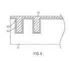
- FIG. 5is a pictorial representation that continues the illustration of the formation of a trench area and an interconnect disposed therein according to various embodiments;
- FIG. 6is a pictorial representation that continues the illustration of the formation of a trench area and an interconnect disposed therein according to various embodiments;
- FIG. 7is a pictorial representation that continues the illustration of the formation of a trench area and an interconnect disposed therein according to various embodiments.
- FIG. 8is a pictorial representation that continues the illustration of the formation of a trench area and an interconnect disposed therein according to various embodiments.
- Depositionis any process that grows, coats, or otherwise transfers a material onto the wafer.
- Available technologiesinclude physical vapor deposition (PVD), chemical vapor deposition (CVD), electrochemical deposition (ECD), molecular beam epitaxy (MBE) and more recently, atomic layer deposition (ALD) among others.
- Removal/etchingis any process that removes material from the wafer. Examples include etch processes (either wet or dry), and chemical-mechanical planarization (CMP), and the like.
- Semiconductor dopingis the modification of electrical properties by doping, for example, transistor sources and drains, generally by diffusion and/or by ion implantation. These doping processes are followed by furnace annealing or by rapid thermal annealing (RTA). Annealing serves to activate the implanted dopants. Films of both conductors (e.g., poly-silicon, aluminum, copper, etc.) and insulators (e.g., various forms of silicon dioxide, silicon nitride, etc.) are used to connect and isolate transistors and their components. Selective doping of various regions of the semiconductor substrate allows the conductivity of the substrate to be changed with the application of voltage. By creating structures of these various components, millions or even billions of transistors can be built and wired together to form the complex circuitry of a modern microelectronic device.
- RTArapid thermal annealing
- semiconductor lithographyi.e., the formation of three-dimensional relief images or patterns on the semiconductor substrate for subsequent transfer of the pattern to the substrate.
- the patternsare on a light sensitive polymer called a photo-resist.
- lithography and etch pattern transfer stepsare repeated multiple times. Each pattern being printed on the wafer is aligned to the previously formed patterns and slowly the conductors, insulators and selectively doped regions are built up to form the final device.
- metal layersare used, for example, to electrically interconnect various devices of the integrated circuit.
- These metal layersmay be, for example, nickel, tungsten, solder, and copper.
- These metalscan be deposited using various different techniques such as, for example, chemical vapor deposition (CVD), physical vapor deposition (PVD), atomic layer deposition, electroplating, and electroless plating, and the like.
- a barrier layermight be formed in patterned structures such as, for example, vias, trenches or other features.
- the barrier layeris used to prevent movement of materials between the circuit patterns into an adjacent dielectric layer.
- the barrier layeris typically tantalum, or tantalum nitride, deposited into the vias and trenches by PVD or ALD processes.
- a copper seed layerfor example, is deposited over the barrier layer and, thereafter, an electroplating process forms the copper interconnect layer.
- An exemplary electromigration blocking boundary of the prior arthad a barrier layer between a via and a metal layer.
- the thickness of the barrier layerpresents a dilemma for semiconductor manufacturers.
- the via resistancemight be high because of the presence of a TaN barrier 122 at the bottom of a via 120 .
- the resistance of the viacan be made lower by removing or thinning the TaN barrier layer.
- the TaN barrier layershould be thick enough such that it works as an electromigration blocking boundary.
- the flow of copper atoms, such as from a metal layer and viacan be blocked by an electromigration blocking boundary.
- the lower level (and upper level, since the blocking boundary works in both directions) metalcan have a much longer electromigration lifetime than prior technology. So semiconductor manufacturers have to balance the thickness of the barrier layer between being thick enough to perform well as an electromigration blocking boundary while being thin enough to present a low via resistance.
- a double-layered copper interconnect structureare used, with a variety of different formation methods.
- the copper interconnectsmight comprise two different conductive materials, a first of which is copper in some embodiments, and a second of which is not.
- the second conductive (non-copper) layer materialcan function as a barrier layer, which obviates the need for a barrier layer between two conductive materials.
- the second conductive layeris cobalt (Co).
- Other materials that can be used for the second conductive layerinclude ruthenium (Ru), tungsten (W), molybdenum (Mo), gold (Au), silver (Ag), aluminum (Al), and various alloys thereof.
- the first conductive materialIn addition to copper (Cu), other materials can be used for the first conductive material, including copper alloys, cobalt (Co), ruthenium (Ru), tungsten (W), molybdenum (Mo), gold (Au), silver (Ag), aluminum (Al), and various alloys thereof.
- copper alloyscobalt (Co), ruthenium (Ru), tungsten (W), molybdenum (Mo), gold (Au), silver (Ag), aluminum (Al), and various alloys thereof.
- Exemplary semiconductor structure 200includes a first conductive layer 210 , a diffusion barrier layer 215 , a second conductive layer 220 and via 225 .
- first conductive layer 210 and via 225are constructed from copper.
- second conductive layer 220is constructed from cobalt.
- the second conductive layercan operate as a diffusion barrier layer, obviating the need for a separate diffusion barrier layer 215 .
- various alloyscan be used as diffusion barrier layer 215 , including the following: tantalum nitride (TaN), titanium nitride (TiN), and cobalt tungsten phosphide (CoWP).
- a second barrier layerthat can be one of a variety of different materials, including: tantalum nitride (TaN), titanium nitride (TiN), pyroxmangite (MnSiO 3 ), and tantalum manganese oxide (TaMnO).
- FIGS. 2 through 8pictorial representations that illustrate the formation of trench area and via holes according to various embodiments are presented.
- FIG. 2shows a dielectric material 310 .
- trench 320 and via 330are also shown.
- the process of forming a double layer barrier layerwill be shown in trench 350 .
- FIG. 3illustrates the formation of a layer on top of dielectric material 310 , within trench 350 .
- FIG. 3is a continuation of FIG. 2 , with the exception that the right-hand portion of FIG. 2 is not shown in FIG. 3 .
- trench 350 or other similar recessmight need to be formed in dielectric 310 .
- trench 350is previously formed in dielectric 310 .
- a layer 452is disposed on dielectric 310 , within trench 350 .
- layer 452might be 5 angstroms to 40 angstroms in thickness.
- layer 452is comprised of TaN and disposed via physical vapor deposition (PVD) or atomic layer deposition (ALD).
- layer 452can comprise titanium nitriade (TiN), pyroxmangite (MnSiO 3 ), or tantalum manganese oxide (TaMnO). In some embodiments, layer 452 might be referred to as a diffusion layer.
- FIG. 4illustrates the formation of a next layer.
- a layer 554 of cobaltis disposed on layer 452 .
- layer 554might serve as a wetting layer.
- cobalt layer 554might be between 5 and 40 angstroms in thickness.
- FIG. 5illustrates the formation of a next layer.
- a first conductive layer 656has been added to the construction of FIG. 4 .
- a copper-manganese seed and electroplatingcan be used for the deposition of first conductive layer 656 .
- first conductive layer 656can be referred to as a copper gap fill layer.
- a variety of different methodscan be used to depose first conductive layer 656 .
- a vacuum continuous depositioncan be used.
- a copper reflowcan be used.
- CMPchemical mechanical planarization
- a barrier layer 860has deposited in recess 758 .
- Atop barrier layer 860is a second conductor layer 862 .
- second conductor layer 862can comprise cobalt.
- other conductorscan be used for second conductor layer 862 . These other conductors can include ruthenium (Ru), tungsten (W), molybdenum (Mo), gold (Au), silver (Ag), aluminum (Al), and various alloys thereof.
- barrier layer 860can comprise tantalum nitride (TaN), titanium nitride (TiN), and cobalt tungsten phosphide (CoWP). As described above, in some embodiments, barrier metal layer 860 might not be needed, depending on the composition of second conductor layer 862 . Thereafter, a chemical mechanical planarization can be performed to finish the processing. The result is illustrated in FIG. 8 .
- the resulting structurehas a relatively low via resistance while also providing a sufficient electromigration barrier.
- the via resistanceis low because there is no high resistance layer at the bottom of the via.
- Electronsflow from another layer through the via to second conductor layer 862 . Then the electron flow disperses in the second conductive layer into the first conductive layer 656 through barrier layer 860 .
- Barrier layer 860works as an electromigration blocking boundary to prevent copper atoms from the upper metal layer from flowing to first conductive layer 656 (and below).
- Barrier layer 860is not at the bottom of the via, but is instead on the top surface of first conductive layer 656 .
- the electronshave a large area the barrier level through which it can travel, lowering the resistance of the via compared to older technologies, while still providing a blocking of electromigration.
- Barrier layer 860also serves as an electromigration redundancy layer. When a copper interconnect causes disconnection due to electromigration, there is a bypass line which can still maintain the electron conductivity. The bypass line is sometimes called the electromigration redundancy layer.
- second conductive layer 862can serve as the electromigration redundancy layer. Barrier layer 860 also serves to prevent cobalt diffusion (from second conductive layer 862 into copper (from first conductive layer 656 ).
Landscapes
- Engineering & Computer Science (AREA)
- Physics & Mathematics (AREA)
- Condensed Matter Physics & Semiconductors (AREA)
- General Physics & Mathematics (AREA)
- Computer Hardware Design (AREA)
- Microelectronics & Electronic Packaging (AREA)
- Power Engineering (AREA)
- Manufacturing & Machinery (AREA)
- Internal Circuitry In Semiconductor Integrated Circuit Devices (AREA)
Abstract
Description
- This application is a division of U.S. application Ser. No. 15/097,033, filed Apr. 12, 2016, the contents of which are hereby incorporated by reference in its entirety.
- The present disclosure relates in general to the field of semiconductor fabrication methodologies and resulting device structures. More specifically, the present disclosure relates to fabrication methodologies and resulting structures for a semiconductor device having a double layered copper interconnect structure.
- Semiconductor devices include a plurality of circuit components (e.g., transistors, resistors, diodes, capacitors, etc.) connected together to form an integrated circuit formed on a semiconductor substrate. A complex network of semiconductor integrated circuit interconnects are routed to connect the circuit components distributed on the surface of the substrate. Efficient routing of these interconnects across semiconductor devices requires the formation of multi-level or multi-layered patterning schemes.
- An interconnect structure includes metal vias that run perpendicular to the semiconductor substrate. The metal vias are disposed in trench areas. In addition, an interconnect structure includes metal lines that are disposed in the trench areas, wherein the trench areas are formed in a dielectric material. The metal vias are connected to the metal lines, and the metal lines run parallel to the semiconductor substrate.
- Furthermore, an interconnect structure that is copper (Cu) based, when compared with an aluminum (Al) based interconnect structure, might provide higher speed signal transmission between large numbers of transistors on a complex semiconductor chip. Accordingly, when manufacturing integrated circuits, copper (i.e., a metal conductor) is typically used for forming the semiconductor integrated circuit's interconnects because of copper's low resistivity and high current carrying capacity. Resistivity is the measure of how much a material opposes electric current caused by a voltage being placed across the material. However, when copper is utilized to form interconnects, electromigration may occur. Electromigration is the gradual displacement of atoms of a metal conductor due to the high density of current passing through the metal conductor.
- For high-speed and low-power operation, the resistance of a via should be low. In addition, the ability to block electromigration should be high. A material such as Tantalum Nitride (TaN) can be used as a barrier layer at the bottom of a via. When the TaN barrier layer is thinned down at the via bottom, the via resistance becomes low. However, that adversely affects the electromigration performance. This is due to no longer having what is called the “short length effect” or “blech length effect.” This is when a copper line with electromigration blocking boundaries is of a sufficiently short length (between 1 to 10 micrometers) that the migrating copper atoms impinge on the blocking boundary creating a stress gradient backwards that prevents further migration of copper. It is desirable to have a blocking boundary layer that provides both low resistance and a high ability to block electromigration.
- Embodiments are directed to a semiconductor interconnect structure. The structure comprises a first conductive layer coupled to a dielectric, a second conductive layer, and a barrier layer disposed between the first conductive layer.
- Embodiments are further directed to a method for forming a semiconductor interconnect structure. The method can comprise forming a first conductive layer in a recess of a dielectric layer and forming a second conductive layer disposed on the first conductive layer.
- Additional features and advantages are realized through techniques described herein. Other embodiments and aspects are described in detail herein. For a better understanding, refer to the description and to the drawings.
- The subject matter which is regarded as embodiments is particularly pointed out and distinctly claimed in the claims at the conclusion of the specification. The foregoing and other features and advantages of the embodiments are apparent from the following detailed description taken in conjunction with the accompanying drawings in which:
FIG. 1 depicts an exemplary double-layer interconnect with a barrier layer of an embodiment;FIG. 2 is a pictorial representation that illustrates the formation of a trench area and an interconnect disposed therein according to various embodiments;FIG. 3 is a pictorial representation that continues the illustration of the formation of a trench area and an interconnect disposed therein according to various embodiments;FIG. 4 is a pictorial representation that continues the illustration of the formation of a trench area and an interconnect disposed therein according to various embodiments;FIG. 5 is a pictorial representation that continues the illustration of the formation of a trench area and an interconnect disposed therein according to various embodiments;FIG. 6 is a pictorial representation that continues the illustration of the formation of a trench area and an interconnect disposed therein according to various embodiments;FIG. 7 is a pictorial representation that continues the illustration of the formation of a trench area and an interconnect disposed therein according to various embodiments; andFIG. 8 is a pictorial representation that continues the illustration of the formation of a trench area and an interconnect disposed therein according to various embodiments.- The drawings are not necessarily to scale. The drawings, some of which are merely pictorial and schematic representations, are not intended to portray specific parameters of the invention. The drawings are intended to depict only typical embodiments of the invention, and therefore should not be considered as limiting. In the drawings, like numbering represents like elements.
- Various embodiments of the present disclosure will now be described with reference to the related drawings. Alternate embodiments may be devised without departing from the scope of this disclosure. Various connections might be set forth between elements in the following description and in the drawings. These connections, unless specified otherwise, may be direct or indirect, and the present disclosure is not intended to be limiting in this respect. Accordingly, a coupling of entities may refer to either a direct or an indirect connection.
- The terminology used herein is for the purpose of describing particular embodiments only and is not intended to be limiting of this disclosure. As used herein, the singular forms “a”, “an”, and “the” are intended to include the plural forms as well, unless the context clearly indicates otherwise. Furthermore, the use of the terms “a”, “an”, etc., do not denote a limitation of quantity, but rather denote the presence of at least one of the referenced items. It will be further understood that the terms “comprises” and/or “comprising”, or “includes” and/or “including”, when used in this specification, specify the presence of stated features, regions, integers, steps, operations, elements, and/or components, but do not preclude the presence or addition of one or more other features, regions, integers, steps, operations, elements, components, and/or groups thereof.
- In addition it will be understood that when an element as a layer, region, or substrate is referred to as being “on” or “over”, or “disposed on” another element, it can be directly on the other element or intervening elements may also be present. In contrast, when an element is referred to as being “directly on”, “directly over”, or “disposed proximately to” another element, there are no intervening elements present. It will also be understood that when an element is referred to as being “connected” or “coupled” to another element, it can be directly connected or directly coupled to the other element, or intervening elements may be present. In contrast, when an element is referred to as being “directly connected” or “directly coupled” to another element, there are no intervening elements present.
- For the sake of brevity, conventional techniques related to semiconductor device and integrated circuit fabrication may not be described in detail herein. Moreover, the various tasks and process steps described herein may be incorporated into a more comprehensive procedure or process having additional steps or functionality not described in detail herein. In particular, various steps in the manufacture of semiconductor devices and semiconductor-based integrated circuits are well-known and so, in the interest of brevity, many conventional steps will only be mentioned briefly herein or will be omitted entirely without providing the well-known process details.
- By way of background, however, a more general description of the semiconductor device fabrication processes that may be utilized in implementing one or more embodiments of the present disclosure will now be provided. Although specific fabrication operations used in implementing one or more embodiments of the present disclosure may be individually known, the disclosed combination of operations and/or resulting structures of the present disclosure are unique. Thus, the unique combination of the operations described in connection with the fabrication of semiconductor devices and I according to the present disclosure utilize a variety of individually known physical and chemical processes performed on a semiconductor (e.g., silicon) substrate, some of which are described in the following immediately following paragraphs.
- In general, the various processes used to form a micro-chip that will be packaged into an integrated circuit fall into four general categories, namely, film deposition, removal/etching, semiconductor doping and patterning/lithography. Deposition is any process that grows, coats, or otherwise transfers a material onto the wafer. Available technologies include physical vapor deposition (PVD), chemical vapor deposition (CVD), electrochemical deposition (ECD), molecular beam epitaxy (MBE) and more recently, atomic layer deposition (ALD) among others. Removal/etching is any process that removes material from the wafer. Examples include etch processes (either wet or dry), and chemical-mechanical planarization (CMP), and the like. Semiconductor doping is the modification of electrical properties by doping, for example, transistor sources and drains, generally by diffusion and/or by ion implantation. These doping processes are followed by furnace annealing or by rapid thermal annealing (RTA). Annealing serves to activate the implanted dopants. Films of both conductors (e.g., poly-silicon, aluminum, copper, etc.) and insulators (e.g., various forms of silicon dioxide, silicon nitride, etc.) are used to connect and isolate transistors and their components. Selective doping of various regions of the semiconductor substrate allows the conductivity of the substrate to be changed with the application of voltage. By creating structures of these various components, millions or even billions of transistors can be built and wired together to form the complex circuitry of a modern microelectronic device.
- Fundamental to the above-described fabrication processes is semiconductor lithography, i.e., the formation of three-dimensional relief images or patterns on the semiconductor substrate for subsequent transfer of the pattern to the substrate. In semiconductor lithography, the patterns are on a light sensitive polymer called a photo-resist. To build the complex structures that make up a transistor and the many wires that connect the millions of transistors of a circuit, lithography and etch pattern transfer steps are repeated multiple times. Each pattern being printed on the wafer is aligned to the previously formed patterns and slowly the conductors, insulators and selectively doped regions are built up to form the final device.
- Turning now to an overview of the present disclosure, the production of semiconductor integrated circuits and other microelectronic devices from semiconductor wafers requires formation of one or more metal layers on a wafer. These metal layers are used, for example, to electrically interconnect various devices of the integrated circuit. These metal layers may be, for example, nickel, tungsten, solder, and copper. These metals can be deposited using various different techniques such as, for example, chemical vapor deposition (CVD), physical vapor deposition (PVD), atomic layer deposition, electroplating, and electroless plating, and the like.
- Prior to the formation of metal interconnects, a barrier layer might be formed in patterned structures such as, for example, vias, trenches or other features. The barrier layer is used to prevent movement of materials between the circuit patterns into an adjacent dielectric layer. The barrier layer is typically tantalum, or tantalum nitride, deposited into the vias and trenches by PVD or ALD processes. After the barrier layer is formed, a copper seed layer, for example, is deposited over the barrier layer and, thereafter, an electroplating process forms the copper interconnect layer.
- An exemplary electromigration blocking boundary of the prior art had a barrier layer between a via and a metal layer. The thickness of the barrier layer presents a dilemma for semiconductor manufacturers. The via resistance might be high because of the presence of a TaN barrier122 at the bottom of a via120. The resistance of the via can be made lower by removing or thinning the TaN barrier layer. However, the TaN barrier layer should be thick enough such that it works as an electromigration blocking boundary. The flow of copper atoms, such as from a metal layer and via, can be blocked by an electromigration blocking boundary. Then the lower level (and upper level, since the blocking boundary works in both directions) metal can have a much longer electromigration lifetime than prior technology. So semiconductor manufacturers have to balance the thickness of the barrier layer between being thick enough to perform well as an electromigration blocking boundary while being thin enough to present a low via resistance.
- Embodiments disclosed herein address the above-described shortcomings. In some embodiments, a double-layered copper interconnect structure are used, with a variety of different formation methods. The copper interconnects might comprise two different conductive materials, a first of which is copper in some embodiments, and a second of which is not. The second conductive (non-copper) layer material can function as a barrier layer, which obviates the need for a barrier layer between two conductive materials. In some embodiments, the second conductive layer is cobalt (Co). Other materials that can be used for the second conductive layer include ruthenium (Ru), tungsten (W), molybdenum (Mo), gold (Au), silver (Ag), aluminum (Al), and various alloys thereof. In addition to copper (Cu), other materials can be used for the first conductive material, including copper alloys, cobalt (Co), ruthenium (Ru), tungsten (W), molybdenum (Mo), gold (Au), silver (Ag), aluminum (Al), and various alloys thereof.
- With reference to
FIG. 1 , an exemplary embodiment of the disclosed barrier layer is presented.Exemplary semiconductor structure 200 includes a first conductive layer210, adiffusion barrier layer 215, a secondconductive layer 220 and via225. In some embodiments, both first conductive layer210 and via225 are constructed from copper. In some embodiments, secondconductive layer 220 is constructed from cobalt. - In some embodiments, the second conductive layer can operate as a diffusion barrier layer, obviating the need for a separate
diffusion barrier layer 215. In other embodiments, various alloys can be used asdiffusion barrier layer 215, including the following: tantalum nitride (TaN), titanium nitride (TiN), and cobalt tungsten phosphide (CoWP). - In some embodiments, there is a second barrier layer that can be one of a variety of different materials, including: tantalum nitride (TaN), titanium nitride (TiN), pyroxmangite (MnSiO3), and tantalum manganese oxide (TaMnO).
- With reference to
FIGS. 2 through 8 , pictorial representations that illustrate the formation of trench area and via holes according to various embodiments are presented. FIG. 2 shows adielectric material 310. For illustrative purposes,trench 320 and via330 are also shown. In the figures that follow, the process of forming a double layer barrier layer will be shown intrench 350.FIG. 3 illustrates the formation of a layer on top ofdielectric material 310, withintrench 350.FIG. 3 is a continuation ofFIG. 2 , with the exception that the right-hand portion ofFIG. 2 is not shown inFIG. 3 . In some embodiments,trench 350 or other similar recess might need to be formed indielectric 310. In other embodiments,trench 350 is previously formed indielectric 310. Alayer 452 is disposed ondielectric 310, withintrench 350. In some embodiments,layer 452 might be 5 angstroms to 40 angstroms in thickness. In some embodiments,layer 452 is comprised of TaN and disposed via physical vapor deposition (PVD) or atomic layer deposition (ALD). In other embodiments, other deposition methods might be used. In other embodiments,layer 452 can comprise titanium nitriade (TiN), pyroxmangite (MnSiO3), or tantalum manganese oxide (TaMnO). In some embodiments,layer 452 might be referred to as a diffusion layer.FIG. 4 illustrates the formation of a next layer. InFIG. 4 , alayer 554 of cobalt is disposed onlayer 452. In some embodiments,layer 554 might serve as a wetting layer. In some embodiments,cobalt layer 554 might be between 5 and 40 angstroms in thickness.FIG. 5 illustrates the formation of a next layer. Here, a firstconductive layer 656 has been added to the construction ofFIG. 4 . In some embodiments, a copper-manganese seed and electroplating can be used for the deposition of firstconductive layer 656. In some embodiments, firstconductive layer 656 can be referred to as a copper gap fill layer. A variety of different methods can be used to depose firstconductive layer 656. In some embodiments, a vacuum continuous deposition can be used. In some embodiments, a copper reflow can be used. Thereafter, a chemical mechanical planarization (CMP) process is performed to removelayers layer 452 will remain on the side wall, some oflayer 554 might be attacked and may or may not be cleared completely on the side wall). The result is shown inFIG. 6 . As shown inFIG. 6 , there might be an overpolish such that arecess 758 is created.- In
FIG. 7 , abarrier layer 860 has deposited inrecess 758. Atopbarrier layer 860 is asecond conductor layer 862. In some embodiments,second conductor layer 862 can comprise cobalt. In other embodiments, other conductors can be used forsecond conductor layer 862. These other conductors can include ruthenium (Ru), tungsten (W), molybdenum (Mo), gold (Au), silver (Ag), aluminum (Al), and various alloys thereof. In some embodiments,barrier layer 860 can comprise tantalum nitride (TaN), titanium nitride (TiN), and cobalt tungsten phosphide (CoWP). As described above, in some embodiments,barrier metal layer 860 might not be needed, depending on the composition ofsecond conductor layer 862. Thereafter, a chemical mechanical planarization can be performed to finish the processing. The result is illustrated inFIG. 8 . - The resulting structure has a relatively low via resistance while also providing a sufficient electromigration barrier. The via resistance is low because there is no high resistance layer at the bottom of the via. Electrons flow from another layer through the via to
second conductor layer 862. Then the electron flow disperses in the second conductive layer into the firstconductive layer 656 throughbarrier layer 860.Barrier layer 860 works as an electromigration blocking boundary to prevent copper atoms from the upper metal layer from flowing to first conductive layer656 (and below).Barrier layer 860 is not at the bottom of the via, but is instead on the top surface of firstconductive layer 656. Thus, the electrons have a large area the barrier level through which it can travel, lowering the resistance of the via compared to older technologies, while still providing a blocking of electromigration. Barrier layer 860 also serves as an electromigration redundancy layer. When a copper interconnect causes disconnection due to electromigration, there is a bypass line which can still maintain the electron conductivity. The bypass line is sometimes called the electromigration redundancy layer. In embodiments disclosed herein, secondconductive layer 862 can serve as the electromigration redundancy layer.Barrier layer 860 also serves to prevent cobalt diffusion (from secondconductive layer 862 into copper (from first conductive layer656).- The terminology used herein is for the purpose of describing particular embodiments only and is not intended to be limiting of the present disclosure. As used herein, the singular forms “a”, “an” and “the” are intended to include the plural forms as well, unless the context clearly indicates otherwise. It will be further understood that the terms “comprises” and/or “comprising,” when used in this specification, specify the presence of stated features, integers, steps, operations, elements, and/or components, but do not preclude the presence or addition of one or more other features, integers, steps, operations, element components, and/or groups thereof.
- The corresponding structures, materials, acts, and equivalents of all means or step plus function elements in the claims below are intended to include any structure, material, or act for performing the function in combination with other claimed elements as specifically claimed. The description of the present disclosure has been presented for purposes of illustration and description, but is not intended to be exhaustive or limited to the disclosure in the form disclosed. Many modifications and variations will be apparent to those of ordinary skill in the art without departing from the scope and spirit of the disclosure. The embodiment was chosen and described in order to best explain the principles of the disclosure and the practical application, and to enable others of ordinary skill in the art to understand the disclosure for various embodiments with various modifications as are suited to the particular use contemplated.
Claims (21)
Priority Applications (3)
| Application Number | Priority Date | Filing Date | Title |
|---|---|---|---|
| US15/609,672US10804193B2 (en) | 2016-04-12 | 2017-05-31 | Semiconductor interconnect structure with double conductors |
| US17/068,230US12087685B2 (en) | 2016-04-12 | 2020-10-12 | Semiconductor interconnect structure with double conductors |
| US18/793,294US20240395702A1 (en) | 2016-04-12 | 2024-08-02 | Semiconductor interconnect structure with double conductors |
Applications Claiming Priority (2)
| Application Number | Priority Date | Filing Date | Title |
|---|---|---|---|
| US15/097,033US9837350B2 (en) | 2016-04-12 | 2016-04-12 | Semiconductor interconnect structure with double conductors |
| US15/609,672US10804193B2 (en) | 2016-04-12 | 2017-05-31 | Semiconductor interconnect structure with double conductors |
Related Parent Applications (1)
| Application Number | Title | Priority Date | Filing Date |
|---|---|---|---|
| US15/097,033DivisionUS9837350B2 (en) | 2016-04-12 | 2016-04-12 | Semiconductor interconnect structure with double conductors |
Related Child Applications (1)
| Application Number | Title | Priority Date | Filing Date |
|---|---|---|---|
| US17/068,230ContinuationUS12087685B2 (en) | 2016-04-12 | 2020-10-12 | Semiconductor interconnect structure with double conductors |
Publications (2)
| Publication Number | Publication Date |
|---|---|
| US20170294382A1true US20170294382A1 (en) | 2017-10-12 |
| US10804193B2 US10804193B2 (en) | 2020-10-13 |
Family
ID=59998849
Family Applications (4)
| Application Number | Title | Priority Date | Filing Date |
|---|---|---|---|
| US15/097,033ActiveUS9837350B2 (en) | 2016-04-12 | 2016-04-12 | Semiconductor interconnect structure with double conductors |
| US15/609,672Active2036-05-17US10804193B2 (en) | 2016-04-12 | 2017-05-31 | Semiconductor interconnect structure with double conductors |
| US17/068,230Active2036-07-17US12087685B2 (en) | 2016-04-12 | 2020-10-12 | Semiconductor interconnect structure with double conductors |
| US18/793,294PendingUS20240395702A1 (en) | 2016-04-12 | 2024-08-02 | Semiconductor interconnect structure with double conductors |
Family Applications Before (1)
| Application Number | Title | Priority Date | Filing Date |
|---|---|---|---|
| US15/097,033ActiveUS9837350B2 (en) | 2016-04-12 | 2016-04-12 | Semiconductor interconnect structure with double conductors |
Family Applications After (2)
| Application Number | Title | Priority Date | Filing Date |
|---|---|---|---|
| US17/068,230Active2036-07-17US12087685B2 (en) | 2016-04-12 | 2020-10-12 | Semiconductor interconnect structure with double conductors |
| US18/793,294PendingUS20240395702A1 (en) | 2016-04-12 | 2024-08-02 | Semiconductor interconnect structure with double conductors |
Country Status (1)
| Country | Link |
|---|---|
| US (4) | US9837350B2 (en) |
Cited By (4)
| Publication number | Priority date | Publication date | Assignee | Title |
|---|---|---|---|---|
| US11100986B2 (en)* | 2019-12-17 | 2021-08-24 | Micron Technology, Inc. | Discharge current mitigation in a memory array |
| US20210335703A1 (en)* | 2017-09-28 | 2021-10-28 | Taiwan Semiconductor Manufacturing Co., Ltd. | Novel mim structure |
| US11417375B2 (en) | 2019-12-17 | 2022-08-16 | Micron Technology, Inc. | Discharge current mitigation in a memory array |
| WO2023116329A1 (en)* | 2021-12-20 | 2023-06-29 | International Business Machines Corporation | Hybrid metal interconnects |
Families Citing this family (8)
| Publication number | Priority date | Publication date | Assignee | Title |
|---|---|---|---|---|
| US10573522B2 (en) | 2016-08-16 | 2020-02-25 | Lam Research Corporation | Method for preventing line bending during metal fill process |
| TWI700799B (en)* | 2016-10-04 | 2020-08-01 | 聯華電子股份有限公司 | Conductive structure, layout structure including conductive structure, and method for manufacturing conductive structure |
| US12148623B2 (en) | 2018-11-19 | 2024-11-19 | Lam Research Corporation | Deposition of tungsten on molybdenum templates |
| CN113366144B (en) | 2019-01-28 | 2023-07-07 | 朗姆研究公司 | Deposition of metal films |
| WO2021046058A1 (en) | 2019-09-03 | 2021-03-11 | Lam Research Corporation | Molybdenum deposition |
| US12327762B2 (en) | 2019-10-15 | 2025-06-10 | Lam Research Corporation | Molybdenum fill |
| US11817389B2 (en) | 2020-03-24 | 2023-11-14 | International Business Machines Corporation | Multi-metal interconnects for semiconductor device structures |
| JP2023550331A (en)* | 2020-11-19 | 2023-12-01 | ラム リサーチ コーポレーション | Low resistivity contacts and interconnects |
Citations (2)
| Publication number | Priority date | Publication date | Assignee | Title |
|---|---|---|---|---|
| US6147404A (en)* | 1999-05-24 | 2000-11-14 | Advanced Micro Devices, Inc. | Dual barrier and conductor deposition in a dual damascene process for semiconductors |
| US20150179579A1 (en)* | 2013-12-20 | 2015-06-25 | Christopher J. Jezewski | Cobalt based interconnects and methods of fabrication thereof |
Family Cites Families (16)
| Publication number | Priority date | Publication date | Assignee | Title |
|---|---|---|---|---|
| KR900003618B1 (en)* | 1986-05-30 | 1990-05-26 | 후지쓰가부시끼가이샤 | Semiconductor device and manufacturing method |
| JP2924450B2 (en)* | 1992-05-22 | 1999-07-26 | 日本電気株式会社 | Semiconductor device |
| US6887353B1 (en) | 1997-12-19 | 2005-05-03 | Applied Materials, Inc. | Tailored barrier layer which provides improved copper interconnect electromigration resistance |
| US20030194857A1 (en) | 2002-04-11 | 2003-10-16 | Stefan Hau-Riege | Method of making a semiconductor device that has copper damascene interconnects with enhanced electromigration reliability |
| US6528409B1 (en)* | 2002-04-29 | 2003-03-04 | Advanced Micro Devices, Inc. | Interconnect structure formed in porous dielectric material with minimized degradation and electromigration |
| US7727892B2 (en) | 2002-09-25 | 2010-06-01 | Intel Corporation | Method and apparatus for forming metal-metal oxide etch stop/barrier for integrated circuit interconnects |
| DE102005046975A1 (en) | 2005-09-30 | 2007-04-05 | Advanced Micro Devices, Inc., Sunnyvale | Process to manufacture a semiconductor component with aperture cut through a dielectric material stack |
| US7569475B2 (en) | 2006-11-15 | 2009-08-04 | International Business Machines Corporation | Interconnect structure having enhanced electromigration reliability and a method of fabricating same |
| US7666781B2 (en) | 2006-11-22 | 2010-02-23 | International Business Machines Corporation | Interconnect structures with improved electromigration resistance and methods for forming such interconnect structures |
| KR20080061030A (en) | 2006-12-27 | 2008-07-02 | 동부일렉트로닉스 주식회사 | Metal wiring formation method of semiconductor device |
| US20090269507A1 (en) | 2008-04-29 | 2009-10-29 | Sang-Ho Yu | Selective cobalt deposition on copper surfaces |
| US8288276B2 (en) | 2008-12-30 | 2012-10-16 | International Business Machines Corporation | Method of forming an interconnect structure including a metallic interfacial layer located at a bottom via portion |
| US8524600B2 (en)* | 2011-03-31 | 2013-09-03 | Applied Materials, Inc. | Post deposition treatments for CVD cobalt films |
| US10163644B2 (en)* | 2014-02-07 | 2018-12-25 | Taiwan Semiconductor Manufacturing Company | Interconnect structure including a conductive feature and a barrier layer on sidewalls and a bottom surface of the conductive feature and method of forming the same |
| US9735051B2 (en)* | 2015-12-14 | 2017-08-15 | International Business Machines Corporation | Semiconductor device interconnect structures formed by metal reflow process |
| KR20170110332A (en)* | 2016-03-23 | 2017-10-11 | 삼성전자주식회사 | Semiconductor devices and methods of manufacturing the same |
- 2016
- 2016-04-12USUS15/097,033patent/US9837350B2/enactiveActive
- 2017
- 2017-05-31USUS15/609,672patent/US10804193B2/enactiveActive
- 2020
- 2020-10-12USUS17/068,230patent/US12087685B2/enactiveActive
- 2024
- 2024-08-02USUS18/793,294patent/US20240395702A1/enactivePending
Patent Citations (2)
| Publication number | Priority date | Publication date | Assignee | Title |
|---|---|---|---|---|
| US6147404A (en)* | 1999-05-24 | 2000-11-14 | Advanced Micro Devices, Inc. | Dual barrier and conductor deposition in a dual damascene process for semiconductors |
| US20150179579A1 (en)* | 2013-12-20 | 2015-06-25 | Christopher J. Jezewski | Cobalt based interconnects and methods of fabrication thereof |
Cited By (5)
| Publication number | Priority date | Publication date | Assignee | Title |
|---|---|---|---|---|
| US20210335703A1 (en)* | 2017-09-28 | 2021-10-28 | Taiwan Semiconductor Manufacturing Co., Ltd. | Novel mim structure |
| US12362271B2 (en)* | 2017-09-28 | 2025-07-15 | Taiwan Semiconductor Manufacturing Company, Ltd. | MIM structure |
| US11100986B2 (en)* | 2019-12-17 | 2021-08-24 | Micron Technology, Inc. | Discharge current mitigation in a memory array |
| US11417375B2 (en) | 2019-12-17 | 2022-08-16 | Micron Technology, Inc. | Discharge current mitigation in a memory array |
| WO2023116329A1 (en)* | 2021-12-20 | 2023-06-29 | International Business Machines Corporation | Hybrid metal interconnects |
Also Published As
| Publication number | Publication date |
|---|---|
| US9837350B2 (en) | 2017-12-05 |
| US20210043563A1 (en) | 2021-02-11 |
| US20170294381A1 (en) | 2017-10-12 |
| US10804193B2 (en) | 2020-10-13 |
| US12087685B2 (en) | 2024-09-10 |
| US20240395702A1 (en) | 2024-11-28 |
Similar Documents
| Publication | Publication Date | Title |
|---|---|---|
| US12087685B2 (en) | Semiconductor interconnect structure with double conductors | |
| US11488862B2 (en) | Semiconductor device with reduced via resistance | |
| US10256186B2 (en) | Interconnect structure having subtractive etch feature and damascene feature | |
| US7666787B2 (en) | Grain growth promotion layer for semiconductor interconnect structures | |
| US6096648A (en) | Copper/low dielectric interconnect formation with reduced electromigration | |
| TWI497673B (en) | Large grain size conductive structure for narrow interconnect openings | |
| US10475742B2 (en) | Method for forming semiconductor device structure having conductive structure with twin boundaries | |
| US8492274B2 (en) | Metal alloy cap integration | |
| US9793206B1 (en) | Heterogeneous metallization using solid diffusion removal of metal interconnects | |
| US20080237800A1 (en) | Integrated circuit having resistor between beol interconnect and feol structure and related method | |
| WO2013126199A1 (en) | Metallic capped interconnect structure with high electromigration resistance and low resistivity | |
| US20130112462A1 (en) | Metal Alloy Cap Integration | |
| US20060228934A1 (en) | Conductive materials for low resistance interconnects and methods of forming the same | |
| US11201112B2 (en) | Fully-aligned skip-vias | |
| US20230197506A1 (en) | Decoupled interconnects | |
| JP2024543595A (en) | Top via interconnect structure with texture suppression layer - Patents.com |
Legal Events
| Date | Code | Title | Description |
|---|---|---|---|
| AS | Assignment | Owner name:INTERNATIONAL BUSINESS MACHINES CORPORATION, NEW YORK Free format text:ASSIGNMENT OF ASSIGNORS INTEREST;ASSIGNORS:BRIGGS, BENJAMIN D.;NOGAMI, TAKESHI;PATLOLLA, RAGHUVEER R.;REEL/FRAME:042547/0245 Effective date:20160411 Owner name:INTERNATIONAL BUSINESS MACHINES CORPORATION, NEW Y Free format text:ASSIGNMENT OF ASSIGNORS INTEREST;ASSIGNORS:BRIGGS, BENJAMIN D.;NOGAMI, TAKESHI;PATLOLLA, RAGHUVEER R.;REEL/FRAME:042547/0245 Effective date:20160411 | |
| STPP | Information on status: patent application and granting procedure in general | Free format text:FINAL REJECTION MAILED | |
| STPP | Information on status: patent application and granting procedure in general | Free format text:RESPONSE AFTER FINAL ACTION FORWARDED TO EXAMINER | |
| STPP | Information on status: patent application and granting procedure in general | Free format text:ADVISORY ACTION MAILED | |
| STPP | Information on status: patent application and granting procedure in general | Free format text:DOCKETED NEW CASE - READY FOR EXAMINATION | |
| STPP | Information on status: patent application and granting procedure in general | Free format text:NON FINAL ACTION MAILED | |
| STPP | Information on status: patent application and granting procedure in general | Free format text:RESPONSE TO NON-FINAL OFFICE ACTION ENTERED AND FORWARDED TO EXAMINER | |
| STPP | Information on status: patent application and granting procedure in general | Free format text:FINAL REJECTION MAILED | |
| STPP | Information on status: patent application and granting procedure in general | Free format text:RESPONSE AFTER FINAL ACTION FORWARDED TO EXAMINER | |
| STPP | Information on status: patent application and granting procedure in general | Free format text:ADVISORY ACTION MAILED | |
| AS | Assignment | Owner name:TESSERA, INC., CALIFORNIA Free format text:ASSIGNMENT OF ASSIGNORS INTEREST;ASSIGNOR:INTERNATIONAL BUSINESS MACHINES CORPORATION;REEL/FRAME:051489/0324 Effective date:20191227 | |
| STPP | Information on status: patent application and granting procedure in general | Free format text:DOCKETED NEW CASE - READY FOR EXAMINATION | |
| STPP | Information on status: patent application and granting procedure in general | Free format text:NON FINAL ACTION MAILED | |
| AS | Assignment | Owner name:BANK OF AMERICA, N.A., NORTH CAROLINA Free format text:SECURITY INTEREST;ASSIGNORS:ROVI SOLUTIONS CORPORATION;ROVI TECHNOLOGIES CORPORATION;ROVI GUIDES, INC.;AND OTHERS;REEL/FRAME:053468/0001 Effective date:20200601 | |
| STPP | Information on status: patent application and granting procedure in general | Free format text:NOTICE OF ALLOWANCE MAILED -- APPLICATION RECEIVED IN OFFICE OF PUBLICATIONS | |
| AS | Assignment | Owner name:TESSERA, INC., CALIFORNIA Free format text:CORRECTIVE ASSIGNMENT TO CORRECT THE 16/161,111 PREVIOUSLY RECORDED ON REEL 051489 FRAME 0324. ASSIGNOR(S) HEREBY CONFIRMS THE ASSIGNMENT;ASSIGNOR:INTERNATIONAL BUSINESS MACHINES CORPORATION;REEL/FRAME:053389/0252 Effective date:20191227 | |
| STPP | Information on status: patent application and granting procedure in general | Free format text:PUBLICATIONS -- ISSUE FEE PAYMENT VERIFIED | |
| STCF | Information on status: patent grant | Free format text:PATENTED CASE | |
| AS | Assignment | Owner name:TESSERA LLC, CALIFORNIA Free format text:CERTIFICATE OF CONVERSION & CHANGE OF NAME;ASSIGNOR:TESSERA, INC.;REEL/FRAME:061388/0199 Effective date:20211001 | |
| MAFP | Maintenance fee payment | Free format text:PAYMENT OF MAINTENANCE FEE, 4TH YEAR, LARGE ENTITY (ORIGINAL EVENT CODE: M1551); ENTITY STATUS OF PATENT OWNER: LARGE ENTITY Year of fee payment:4 | |
| AS | Assignment | Owner name:ADEIA SEMICONDUCTOR SOLUTIONS LLC, CALIFORNIA Free format text:CHANGE OF NAME;ASSIGNOR:TESSERA LLC;REEL/FRAME:069067/0448 Effective date:20220815 |